EP3257906A1 - Interlayer composition for electronic printing - Google Patents
Interlayer composition for electronic printing Download PDFInfo
- Publication number
- EP3257906A1 EP3257906A1 EP17172581.5A EP17172581A EP3257906A1 EP 3257906 A1 EP3257906 A1 EP 3257906A1 EP 17172581 A EP17172581 A EP 17172581A EP 3257906 A1 EP3257906 A1 EP 3257906A1
- Authority
- EP
- European Patent Office
- Prior art keywords
- weight percent
- composition
- melamine
- formaldehyde
- poly
- Prior art date
- Legal status (The legal status is an assumption and is not a legal conclusion. Google has not performed a legal analysis and makes no representation as to the accuracy of the status listed.)
- Granted
Links
- 239000000203 mixture Substances 0.000 title claims abstract description 110
- 239000011229 interlayer Substances 0.000 title claims description 51
- 238000007639 printing Methods 0.000 title description 5
- 229920002037 poly(vinyl butyral) polymer Polymers 0.000 claims abstract description 42
- 229920000642 polymer Polymers 0.000 claims abstract description 40
- WSFSSNUMVMOOMR-UHFFFAOYSA-N formaldehyde Substances O=C WSFSSNUMVMOOMR-UHFFFAOYSA-N 0.000 claims abstract description 39
- 150000008064 anhydrides Chemical class 0.000 claims abstract description 20
- 239000000758 substrate Substances 0.000 claims description 53
- -1 polyethylene naphthalate Polymers 0.000 claims description 35
- 239000011521 glass Substances 0.000 claims description 30
- 239000011112 polyethylene naphthalate Substances 0.000 claims description 12
- 239000002105 nanoparticle Substances 0.000 claims description 9
- 229920003207 poly(ethylene-2,6-naphthalate) Polymers 0.000 claims description 9
- 239000000976 ink Substances 0.000 description 38
- 229920000647 polyepoxide Polymers 0.000 description 27
- 239000003822 epoxy resin Substances 0.000 description 24
- BQCADISMDOOEFD-UHFFFAOYSA-N Silver Chemical compound [Ag] BQCADISMDOOEFD-UHFFFAOYSA-N 0.000 description 21
- 239000010408 film Substances 0.000 description 21
- 229910052709 silver Inorganic materials 0.000 description 18
- 239000004332 silver Substances 0.000 description 18
- 238000000034 method Methods 0.000 description 16
- LNEPOXFFQSENCJ-UHFFFAOYSA-N haloperidol Chemical compound C1CC(O)(C=2C=CC(Cl)=CC=2)CCN1CCCC(=O)C1=CC=C(F)C=C1 LNEPOXFFQSENCJ-UHFFFAOYSA-N 0.000 description 15
- 238000010438 heat treatment Methods 0.000 description 15
- WFDIJRYMOXRFFG-UHFFFAOYSA-N Acetic anhydride Chemical compound CC(=O)OC(C)=O WFDIJRYMOXRFFG-UHFFFAOYSA-N 0.000 description 12
- 229920000877 Melamine resin Polymers 0.000 description 12
- 239000003054 catalyst Substances 0.000 description 12
- 239000004205 dimethyl polysiloxane Substances 0.000 description 12
- 229920000435 poly(dimethylsiloxane) Polymers 0.000 description 12
- 239000007787 solid Substances 0.000 description 12
- GYZLOYUZLJXAJU-UHFFFAOYSA-N diglycidyl ether Chemical compound C1OC1COCC1CO1 GYZLOYUZLJXAJU-UHFFFAOYSA-N 0.000 description 11
- 238000000151 deposition Methods 0.000 description 9
- IVJISJACKSSFGE-UHFFFAOYSA-N formaldehyde;1,3,5-triazine-2,4,6-triamine Chemical compound O=C.NC1=NC(N)=NC(N)=N1 IVJISJACKSSFGE-UHFFFAOYSA-N 0.000 description 9
- 239000010410 layer Substances 0.000 description 9
- 239000002904 solvent Substances 0.000 description 9
- 239000004094 surface-active agent Substances 0.000 description 9
- 239000004721 Polyphenylene oxide Substances 0.000 description 8
- 229920000570 polyether Polymers 0.000 description 8
- FOIXSVOLVBLSDH-UHFFFAOYSA-N Silver ion Chemical compound [Ag+] FOIXSVOLVBLSDH-UHFFFAOYSA-N 0.000 description 7
- 229910052751 metal Inorganic materials 0.000 description 7
- 239000002184 metal Substances 0.000 description 7
- BRLQWZUYTZBJKN-UHFFFAOYSA-N Epichlorohydrin Chemical compound ClCC1CO1 BRLQWZUYTZBJKN-UHFFFAOYSA-N 0.000 description 6
- HEMHJVSKTPXQMS-UHFFFAOYSA-M Sodium hydroxide Chemical compound [OH-].[Na+] HEMHJVSKTPXQMS-UHFFFAOYSA-M 0.000 description 6
- YXFVVABEGXRONW-UHFFFAOYSA-N Toluene Chemical compound CC1=CC=CC=C1 YXFVVABEGXRONW-UHFFFAOYSA-N 0.000 description 6
- 125000003118 aryl group Chemical group 0.000 description 6
- PXKLMJQFEQBVLD-UHFFFAOYSA-N bisphenol F Chemical compound C1=CC(O)=CC=C1CC1=CC=C(O)C=C1 PXKLMJQFEQBVLD-UHFFFAOYSA-N 0.000 description 6
- 238000009472 formulation Methods 0.000 description 6
- 239000002082 metal nanoparticle Substances 0.000 description 6
- 229920000728 polyester Polymers 0.000 description 6
- 229920002451 polyvinyl alcohol Polymers 0.000 description 6
- LLHKCFNBLRBOGN-UHFFFAOYSA-N propylene glycol methyl ether acetate Chemical compound COCC(C)OC(C)=O LLHKCFNBLRBOGN-UHFFFAOYSA-N 0.000 description 6
- 229920005989 resin Polymers 0.000 description 6
- 239000011347 resin Substances 0.000 description 6
- 239000000126 substance Substances 0.000 description 6
- 239000004593 Epoxy Substances 0.000 description 5
- ISWSIDIOOBJBQZ-UHFFFAOYSA-N Phenol Chemical compound OC1=CC=CC=C1 ISWSIDIOOBJBQZ-UHFFFAOYSA-N 0.000 description 5
- 239000004372 Polyvinyl alcohol Substances 0.000 description 5
- 238000000137 annealing Methods 0.000 description 5
- IISBACLAFKSPIT-UHFFFAOYSA-N bisphenol A Chemical compound C=1C=C(O)C=CC=1C(C)(C)C1=CC=C(O)C=C1 IISBACLAFKSPIT-UHFFFAOYSA-N 0.000 description 5
- 239000011248 coating agent Substances 0.000 description 5
- 238000000576 coating method Methods 0.000 description 5
- 150000002118 epoxides Chemical class 0.000 description 5
- 239000000463 material Substances 0.000 description 5
- 229920003986 novolac Polymers 0.000 description 5
- ZTQSAGDEMFDKMZ-UHFFFAOYSA-N Butyraldehyde Chemical compound CCCC=O ZTQSAGDEMFDKMZ-UHFFFAOYSA-N 0.000 description 4
- 229920001665 Poly-4-vinylphenol Polymers 0.000 description 4
- 239000004844 aliphatic epoxy resin Substances 0.000 description 4
- 238000006243 chemical reaction Methods 0.000 description 4
- 150000001875 compounds Chemical class 0.000 description 4
- 239000004020 conductor Substances 0.000 description 4
- 125000003700 epoxy group Chemical group 0.000 description 4
- 229920001451 polypropylene glycol Polymers 0.000 description 4
- 229920002689 polyvinyl acetate Polymers 0.000 description 4
- 239000011118 polyvinyl acetate Substances 0.000 description 4
- 239000000843 powder Substances 0.000 description 4
- UHOVQNZJYSORNB-UHFFFAOYSA-N Benzene Chemical compound C1=CC=CC=C1 UHOVQNZJYSORNB-UHFFFAOYSA-N 0.000 description 3
- LRHPLDYGYMQRHN-UHFFFAOYSA-N N-Butanol Chemical compound CCCCO LRHPLDYGYMQRHN-UHFFFAOYSA-N 0.000 description 3
- 229940106691 bisphenol a Drugs 0.000 description 3
- 125000003055 glycidyl group Chemical group C(C1CO1)* 0.000 description 3
- 238000007641 inkjet printing Methods 0.000 description 3
- 238000004519 manufacturing process Methods 0.000 description 3
- 238000002156 mixing Methods 0.000 description 3
- 229920000058 polyacrylate Polymers 0.000 description 3
- 230000005855 radiation Effects 0.000 description 3
- WBIQQQGBSDOWNP-UHFFFAOYSA-N 2-dodecylbenzenesulfonic acid Chemical compound CCCCCCCCCCCCC1=CC=CC=C1S(O)(=O)=O WBIQQQGBSDOWNP-UHFFFAOYSA-N 0.000 description 2
- CCTFMNIEFHGTDU-UHFFFAOYSA-N 3-methoxypropyl acetate Chemical compound COCCCOC(C)=O CCTFMNIEFHGTDU-UHFFFAOYSA-N 0.000 description 2
- XKRFYHLGVUSROY-UHFFFAOYSA-N Argon Chemical compound [Ar] XKRFYHLGVUSROY-UHFFFAOYSA-N 0.000 description 2
- IJGRMHOSHXDMSA-UHFFFAOYSA-N Atomic nitrogen Chemical compound N#N IJGRMHOSHXDMSA-UHFFFAOYSA-N 0.000 description 2
- YNQLUTRBYVCPMQ-UHFFFAOYSA-N Ethylbenzene Chemical compound CCC1=CC=CC=C1 YNQLUTRBYVCPMQ-UHFFFAOYSA-N 0.000 description 2
- CTQNGGLPUBDAKN-UHFFFAOYSA-N O-Xylene Chemical compound CC1=CC=CC=C1C CTQNGGLPUBDAKN-UHFFFAOYSA-N 0.000 description 2
- KFSLWBXXFJQRDL-UHFFFAOYSA-N Peracetic acid Chemical compound CC(=O)OO KFSLWBXXFJQRDL-UHFFFAOYSA-N 0.000 description 2
- 239000004642 Polyimide Substances 0.000 description 2
- 150000008065 acid anhydrides Chemical class 0.000 description 2
- 230000002378 acidificating effect Effects 0.000 description 2
- 239000012298 atmosphere Substances 0.000 description 2
- 230000015572 biosynthetic process Effects 0.000 description 2
- 238000006482 condensation reaction Methods 0.000 description 2
- 230000008021 deposition Effects 0.000 description 2
- 229940060296 dodecylbenzenesulfonic acid Drugs 0.000 description 2
- 230000009477 glass transition Effects 0.000 description 2
- 239000001257 hydrogen Substances 0.000 description 2
- 229910052739 hydrogen Inorganic materials 0.000 description 2
- 125000002887 hydroxy group Chemical group [H]O* 0.000 description 2
- JDSHMPZPIAZGSV-UHFFFAOYSA-N melamine Chemical class NC1=NC(N)=NC(N)=N1 JDSHMPZPIAZGSV-UHFFFAOYSA-N 0.000 description 2
- 239000002923 metal particle Substances 0.000 description 2
- 125000002496 methyl group Chemical group [H]C([H])([H])* 0.000 description 2
- 229920003023 plastic Polymers 0.000 description 2
- 239000004033 plastic Substances 0.000 description 2
- 229920000139 polyethylene terephthalate Polymers 0.000 description 2
- 239000005020 polyethylene terephthalate Substances 0.000 description 2
- 229920001721 polyimide Polymers 0.000 description 2
- 229920001296 polysiloxane Polymers 0.000 description 2
- 239000010703 silicon Substances 0.000 description 2
- 229910052710 silicon Inorganic materials 0.000 description 2
- 238000010129 solution processing Methods 0.000 description 2
- 238000004528 spin coating Methods 0.000 description 2
- 238000012546 transfer Methods 0.000 description 2
- HGBOYTHUEUWSSQ-UHFFFAOYSA-N valeric aldehyde Natural products CCCCC=O HGBOYTHUEUWSSQ-UHFFFAOYSA-N 0.000 description 2
- XLYOFNOQVPJJNP-UHFFFAOYSA-N water Substances O XLYOFNOQVPJJNP-UHFFFAOYSA-N 0.000 description 2
- 239000008096 xylene Substances 0.000 description 2
- DNIAPMSPPWPWGF-VKHMYHEASA-N (+)-propylene glycol Chemical compound C[C@H](O)CO DNIAPMSPPWPWGF-VKHMYHEASA-N 0.000 description 1
- HCITUYXHCZGFEO-UHFFFAOYSA-N 1,3,5-triazine-2,4,6-triamine Chemical compound NC1=NC(N)=NC(N)=N1.N=C1NC(=N)NC(=N)N1 HCITUYXHCZGFEO-UHFFFAOYSA-N 0.000 description 1
- GVJRTUUUJYMTNQ-UHFFFAOYSA-N 2-(2,5-dioxofuran-3-yl)acetic acid Chemical compound OC(=O)CC1=CC(=O)OC1=O GVJRTUUUJYMTNQ-UHFFFAOYSA-N 0.000 description 1
- VXHYVVAUHMGCEX-UHFFFAOYSA-N 2-(2-hydroxyphenoxy)phenol Chemical compound OC1=CC=CC=C1OC1=CC=CC=C1O VXHYVVAUHMGCEX-UHFFFAOYSA-N 0.000 description 1
- WAEVWDZKMBQDEJ-UHFFFAOYSA-N 2-[2-(2-methoxypropoxy)propoxy]propan-1-ol Chemical compound COC(C)COC(C)COC(C)CO WAEVWDZKMBQDEJ-UHFFFAOYSA-N 0.000 description 1
- MROZYFGXESLRQQ-UHFFFAOYSA-N 2-[3-[4-[2-[4-[3-(oxiran-2-ylmethoxy)propoxy]phenyl]propan-2-yl]phenoxy]propoxymethyl]oxirane Chemical compound C=1C=C(OCCCOCC2OC2)C=CC=1C(C)(C)C(C=C1)=CC=C1OCCCOCC1CO1 MROZYFGXESLRQQ-UHFFFAOYSA-N 0.000 description 1
- GFPCHXLNBRGOSJ-UHFFFAOYSA-N 2-[[2-bromo-4-[2-[3-bromo-4-(oxiran-2-ylmethoxy)phenyl]propan-2-yl]phenoxy]methyl]oxirane Chemical compound C=1C=C(OCC2OC2)C(Br)=CC=1C(C)(C)C(C=C1Br)=CC=C1OCC1CO1 GFPCHXLNBRGOSJ-UHFFFAOYSA-N 0.000 description 1
- LJBWJFWNFUKAGS-UHFFFAOYSA-N 2-[bis(2-hydroxyphenyl)methyl]phenol Chemical compound OC1=CC=CC=C1C(C=1C(=CC=CC=1)O)C1=CC=CC=C1O LJBWJFWNFUKAGS-UHFFFAOYSA-N 0.000 description 1
- CBECDWUDYQOTSW-UHFFFAOYSA-N 2-ethylbut-3-enal Chemical group CCC(C=C)C=O CBECDWUDYQOTSW-UHFFFAOYSA-N 0.000 description 1
- QTWJRLJHJPIABL-UHFFFAOYSA-N 2-methylphenol;3-methylphenol;4-methylphenol Chemical compound CC1=CC=C(O)C=C1.CC1=CC=CC(O)=C1.CC1=CC=CC=C1O QTWJRLJHJPIABL-UHFFFAOYSA-N 0.000 description 1
- QCAHUFWKIQLBNB-UHFFFAOYSA-N 3-(3-methoxypropoxy)propan-1-ol Chemical compound COCCCOCCCO QCAHUFWKIQLBNB-UHFFFAOYSA-N 0.000 description 1
- AYKYXWQEBUNJCN-UHFFFAOYSA-N 3-methylfuran-2,5-dione Chemical compound CC1=CC(=O)OC1=O AYKYXWQEBUNJCN-UHFFFAOYSA-N 0.000 description 1
- OFNISBHGPNMTMS-UHFFFAOYSA-N 3-methylideneoxolane-2,5-dione Chemical compound C=C1CC(=O)OC1=O OFNISBHGPNMTMS-UHFFFAOYSA-N 0.000 description 1
- MECNWXGGNCJFQJ-UHFFFAOYSA-N 3-piperidin-1-ylpropane-1,2-diol Chemical compound OCC(O)CN1CCCCC1 MECNWXGGNCJFQJ-UHFFFAOYSA-N 0.000 description 1
- FAUAZXVRLVIARB-UHFFFAOYSA-N 4-[[4-[bis(oxiran-2-ylmethyl)amino]phenyl]methyl]-n,n-bis(oxiran-2-ylmethyl)aniline Chemical group C1OC1CN(C=1C=CC(CC=2C=CC(=CC=2)N(CC2OC2)CC2OC2)=CC=1)CC1CO1 FAUAZXVRLVIARB-UHFFFAOYSA-N 0.000 description 1
- WWJAZKZLSDRAIV-UHFFFAOYSA-N 4-fluoro-2-benzofuran-1,3-dione Chemical compound FC1=CC=CC2=C1C(=O)OC2=O WWJAZKZLSDRAIV-UHFFFAOYSA-N 0.000 description 1
- NHJIDZUQMHKGRE-UHFFFAOYSA-N 7-oxabicyclo[4.1.0]heptan-4-yl 2-(7-oxabicyclo[4.1.0]heptan-4-yl)acetate Chemical compound C1CC2OC2CC1OC(=O)CC1CC2OC2CC1 NHJIDZUQMHKGRE-UHFFFAOYSA-N 0.000 description 1
- QTBSBXVTEAMEQO-UHFFFAOYSA-M Acetate Chemical compound CC([O-])=O QTBSBXVTEAMEQO-UHFFFAOYSA-M 0.000 description 1
- QTBSBXVTEAMEQO-UHFFFAOYSA-N Acetic acid Chemical group CC(O)=O QTBSBXVTEAMEQO-UHFFFAOYSA-N 0.000 description 1
- LSNNMFCWUKXFEE-UHFFFAOYSA-M Bisulfite Chemical compound OS([O-])=O LSNNMFCWUKXFEE-UHFFFAOYSA-M 0.000 description 1
- DKPFZGUDAPQIHT-UHFFFAOYSA-N Butyl acetate Natural products CCCCOC(C)=O DKPFZGUDAPQIHT-UHFFFAOYSA-N 0.000 description 1
- FXHRKJAHRHGJLB-UHFFFAOYSA-N CC(C)(c(cc1)ccc1OCCCOCCC1OC1)c(cc1)ccc1OCCCOCC1OC1 Chemical compound CC(C)(c(cc1)ccc1OCCCOCCC1OC1)c(cc1)ccc1OCCCOCC1OC1 FXHRKJAHRHGJLB-UHFFFAOYSA-N 0.000 description 1
- LFQSCWFLJHTTHZ-UHFFFAOYSA-N Ethanol Chemical compound CCO LFQSCWFLJHTTHZ-UHFFFAOYSA-N 0.000 description 1
- UFHFLCQGNIYNRP-UHFFFAOYSA-N Hydrogen Chemical compound [H][H] UFHFLCQGNIYNRP-UHFFFAOYSA-N 0.000 description 1
- 239000004640 Melamine resin Substances 0.000 description 1
- NTIZESTWPVYFNL-UHFFFAOYSA-N Methyl isobutyl ketone Chemical compound CC(C)CC(C)=O NTIZESTWPVYFNL-UHFFFAOYSA-N 0.000 description 1
- UIHCLUNTQKBZGK-UHFFFAOYSA-N Methyl isobutyl ketone Natural products CCC(C)C(C)=O UIHCLUNTQKBZGK-UHFFFAOYSA-N 0.000 description 1
- LGRFSURHDFAFJT-UHFFFAOYSA-N Phthalic anhydride Natural products C1=CC=C2C(=O)OC(=O)C2=C1 LGRFSURHDFAFJT-UHFFFAOYSA-N 0.000 description 1
- XTXRWKRVRITETP-UHFFFAOYSA-N Vinyl acetate Chemical group CC(=O)OC=C XTXRWKRVRITETP-UHFFFAOYSA-N 0.000 description 1
- 239000000654 additive Substances 0.000 description 1
- 230000000996 additive effect Effects 0.000 description 1
- 239000002318 adhesion promoter Substances 0.000 description 1
- 230000002411 adverse Effects 0.000 description 1
- 150000007933 aliphatic carboxylic acids Chemical class 0.000 description 1
- 125000001931 aliphatic group Chemical group 0.000 description 1
- 239000003513 alkali Substances 0.000 description 1
- 125000000217 alkyl group Chemical group 0.000 description 1
- 150000001412 amines Chemical class 0.000 description 1
- 238000013459 approach Methods 0.000 description 1
- 229910052786 argon Inorganic materials 0.000 description 1
- 150000004982 aromatic amines Chemical class 0.000 description 1
- 150000004945 aromatic hydrocarbons Chemical class 0.000 description 1
- 125000003710 aryl alkyl group Chemical group 0.000 description 1
- YKOQAAJBYBTSBS-UHFFFAOYSA-N biphenyl-2,3-diol Chemical class OC1=CC=CC(C=2C=CC=CC=2)=C1O YKOQAAJBYBTSBS-UHFFFAOYSA-N 0.000 description 1
- DJUWPHRCMMMSCV-UHFFFAOYSA-N bis(7-oxabicyclo[4.1.0]heptan-4-ylmethyl) hexanedioate Chemical compound C1CC2OC2CC1COC(=O)CCCCC(=O)OCC1CC2OC2CC1 DJUWPHRCMMMSCV-UHFFFAOYSA-N 0.000 description 1
- 239000004841 bisphenol A epoxy resin Substances 0.000 description 1
- JHIWVOJDXOSYLW-UHFFFAOYSA-N butyl 2,2-difluorocyclopropane-1-carboxylate Chemical compound CCCCOC(=O)C1CC1(F)F JHIWVOJDXOSYLW-UHFFFAOYSA-N 0.000 description 1
- 229940043232 butyl acetate Drugs 0.000 description 1
- 125000000484 butyl group Chemical group [H]C([*])([H])C([H])([H])C([H])([H])C([H])([H])[H] 0.000 description 1
- 238000012512 characterization method Methods 0.000 description 1
- XENVCRGQTABGKY-ZHACJKMWSA-N chlorohydrin Chemical compound CC#CC#CC#CC#C\C=C\C(Cl)CO XENVCRGQTABGKY-ZHACJKMWSA-N 0.000 description 1
- 238000004581 coalescence Methods 0.000 description 1
- 229930003836 cresol Natural products 0.000 description 1
- 150000001896 cresols Chemical class 0.000 description 1
- 238000004132 cross linking Methods 0.000 description 1
- 239000003431 cross linking reagent Substances 0.000 description 1
- 239000011353 cycloaliphatic epoxy resin Substances 0.000 description 1
- 150000001925 cycloalkenes Chemical class 0.000 description 1
- IGARGHRYKHJQSM-UHFFFAOYSA-N cyclohexylbenzene Chemical compound C1CCCCC1C1=CC=CC=C1 IGARGHRYKHJQSM-UHFFFAOYSA-N 0.000 description 1
- WVIIMZNLDWSIRH-UHFFFAOYSA-N cyclohexylcyclohexane Chemical compound C1CCCCC1C1CCCCC1 WVIIMZNLDWSIRH-UHFFFAOYSA-N 0.000 description 1
- 230000003247 decreasing effect Effects 0.000 description 1
- 238000007033 dehydrochlorination reaction Methods 0.000 description 1
- 150000001990 dicarboxylic acid derivatives Chemical class 0.000 description 1
- 238000003618 dip coating Methods 0.000 description 1
- 238000005441 electronic device fabrication Methods 0.000 description 1
- 238000005516 engineering process Methods 0.000 description 1
- LDLDYFCCDKENPD-UHFFFAOYSA-N ethenylcyclohexane Chemical compound C=CC1CCCCC1 LDLDYFCCDKENPD-UHFFFAOYSA-N 0.000 description 1
- RTZKZFJDLAIYFH-UHFFFAOYSA-N ether Substances CCOCC RTZKZFJDLAIYFH-UHFFFAOYSA-N 0.000 description 1
- 125000001495 ethyl group Chemical group [H]C([H])([H])C([H])([H])* 0.000 description 1
- 239000004744 fabric Substances 0.000 description 1
- 229920002457 flexible plastic Polymers 0.000 description 1
- 239000004845 glycidylamine epoxy resin Substances 0.000 description 1
- 238000007646 gravure printing Methods 0.000 description 1
- 125000000623 heterocyclic group Chemical group 0.000 description 1
- FUZZWVXGSFPDMH-UHFFFAOYSA-N hexanoic acid Chemical compound CCCCCC(O)=O FUZZWVXGSFPDMH-UHFFFAOYSA-N 0.000 description 1
- 125000004051 hexyl group Chemical group [H]C([H])([H])C([H])([H])C([H])([H])C([H])([H])C([H])([H])C([H])([H])* 0.000 description 1
- 150000002431 hydrogen Chemical group 0.000 description 1
- 230000007062 hydrolysis Effects 0.000 description 1
- 238000006460 hydrolysis reaction Methods 0.000 description 1
- 230000010354 integration Effects 0.000 description 1
- 125000000959 isobutyl group Chemical group [H]C([H])([H])C([H])(C([H])([H])[H])C([H])([H])* 0.000 description 1
- 125000001449 isopropyl group Chemical group [H]C([H])([H])C([H])(*)C([H])([H])[H] 0.000 description 1
- 239000007788 liquid Substances 0.000 description 1
- FPYJFEHAWHCUMM-UHFFFAOYSA-N maleic anhydride Chemical compound O=C1OC(=O)C=C1 FPYJFEHAWHCUMM-UHFFFAOYSA-N 0.000 description 1
- 238000005259 measurement Methods 0.000 description 1
- YDKNBNOOCSNPNS-UHFFFAOYSA-N methyl 1,3-benzoxazole-2-carboxylate Chemical compound C1=CC=C2OC(C(=O)OC)=NC2=C1 YDKNBNOOCSNPNS-UHFFFAOYSA-N 0.000 description 1
- SLCVBVWXLSEKPL-UHFFFAOYSA-N neopentyl glycol Chemical compound OCC(C)(C)CO SLCVBVWXLSEKPL-UHFFFAOYSA-N 0.000 description 1
- 229910052757 nitrogen Inorganic materials 0.000 description 1
- QJGQUHMNIGDVPM-UHFFFAOYSA-N nitrogen group Chemical group [N] QJGQUHMNIGDVPM-UHFFFAOYSA-N 0.000 description 1
- 239000004843 novolac epoxy resin Substances 0.000 description 1
- 238000007645 offset printing Methods 0.000 description 1
- 125000000466 oxiranyl group Chemical group 0.000 description 1
- 239000002245 particle Substances 0.000 description 1
- 238000000059 patterning Methods 0.000 description 1
- 239000008188 pellet Substances 0.000 description 1
- 125000001147 pentyl group Chemical group C(CCCC)* 0.000 description 1
- 238000005502 peroxidation Methods 0.000 description 1
- 150000004965 peroxy acids Chemical class 0.000 description 1
- 150000002989 phenols Chemical class 0.000 description 1
- 239000002985 plastic film Substances 0.000 description 1
- 229920006255 plastic film Polymers 0.000 description 1
- 229920000515 polycarbonate Polymers 0.000 description 1
- 239000004417 polycarbonate Substances 0.000 description 1
- 229920005862 polyol Polymers 0.000 description 1
- 150000003077 polyols Chemical class 0.000 description 1
- 125000001436 propyl group Chemical group [H]C([*])([H])C([H])([H])C([H])([H])[H] 0.000 description 1
- 239000011342 resin composition Substances 0.000 description 1
- 238000007650 screen-printing Methods 0.000 description 1
- 238000005245 sintering Methods 0.000 description 1
- 238000007764 slot die coating Methods 0.000 description 1
- 239000011877 solvent mixture Substances 0.000 description 1
- 238000005507 spraying Methods 0.000 description 1
- 238000003892 spreading Methods 0.000 description 1
- 230000003746 surface roughness Effects 0.000 description 1
- 238000012360 testing method Methods 0.000 description 1
- 239000010409 thin film Substances 0.000 description 1
- JOXIMZWYDAKGHI-UHFFFAOYSA-N toluene-4-sulfonic acid Chemical class CC1=CC=C(S(O)(=O)=O)C=C1 JOXIMZWYDAKGHI-UHFFFAOYSA-N 0.000 description 1
- 150000004072 triols Chemical class 0.000 description 1
- 238000009736 wetting Methods 0.000 description 1
Images


Classifications
-
- C—CHEMISTRY; METALLURGY
- C09—DYES; PAINTS; POLISHES; NATURAL RESINS; ADHESIVES; COMPOSITIONS NOT OTHERWISE PROVIDED FOR; APPLICATIONS OF MATERIALS NOT OTHERWISE PROVIDED FOR
- C09D—COATING COMPOSITIONS, e.g. PAINTS, VARNISHES OR LACQUERS; FILLING PASTES; CHEMICAL PAINT OR INK REMOVERS; INKS; CORRECTING FLUIDS; WOODSTAINS; PASTES OR SOLIDS FOR COLOURING OR PRINTING; USE OF MATERIALS THEREFOR
- C09D129/00—Coating compositions based on homopolymers or copolymers of compounds having one or more unsaturated aliphatic radicals, each having only one carbon-to-carbon double bond, and at least one being terminated by an alcohol, ether, aldehydo, ketonic, acetal, or ketal radical; Coating compositions based on hydrolysed polymers of esters of unsaturated alcohols with saturated carboxylic acids; Coating compositions based on derivatives of such polymers
- C09D129/14—Homopolymers or copolymers of acetals or ketals obtained by polymerisation of unsaturated acetals or ketals or by after-treatment of polymers of unsaturated alcohols
-
- B—PERFORMING OPERATIONS; TRANSPORTING
- B32—LAYERED PRODUCTS
- B32B—LAYERED PRODUCTS, i.e. PRODUCTS BUILT-UP OF STRATA OF FLAT OR NON-FLAT, e.g. CELLULAR OR HONEYCOMB, FORM
- B32B27/00—Layered products comprising a layer of synthetic resin
- B32B27/42—Layered products comprising a layer of synthetic resin comprising condensation resins of aldehydes, e.g. with phenols, ureas or melamines
-
- B—PERFORMING OPERATIONS; TRANSPORTING
- B32—LAYERED PRODUCTS
- B32B—LAYERED PRODUCTS, i.e. PRODUCTS BUILT-UP OF STRATA OF FLAT OR NON-FLAT, e.g. CELLULAR OR HONEYCOMB, FORM
- B32B7/00—Layered products characterised by the relation between layers; Layered products characterised by the relative orientation of features between layers, or by the relative values of a measurable parameter between layers, i.e. products comprising layers having different physical, chemical or physicochemical properties; Layered products characterised by the interconnection of layers
- B32B7/04—Interconnection of layers
- B32B7/12—Interconnection of layers using interposed adhesives or interposed materials with bonding properties
-
- C—CHEMISTRY; METALLURGY
- C08—ORGANIC MACROMOLECULAR COMPOUNDS; THEIR PREPARATION OR CHEMICAL WORKING-UP; COMPOSITIONS BASED THEREON
- C08J—WORKING-UP; GENERAL PROCESSES OF COMPOUNDING; AFTER-TREATMENT NOT COVERED BY SUBCLASSES C08B, C08C, C08F, C08G or C08H
- C08J5/00—Manufacture of articles or shaped materials containing macromolecular substances
- C08J5/18—Manufacture of films or sheets
-
- C—CHEMISTRY; METALLURGY
- C08—ORGANIC MACROMOLECULAR COMPOUNDS; THEIR PREPARATION OR CHEMICAL WORKING-UP; COMPOSITIONS BASED THEREON
- C08J—WORKING-UP; GENERAL PROCESSES OF COMPOUNDING; AFTER-TREATMENT NOT COVERED BY SUBCLASSES C08B, C08C, C08F, C08G or C08H
- C08J7/00—Chemical treatment or coating of shaped articles made of macromolecular substances
- C08J7/04—Coating
- C08J7/042—Coating with two or more layers, where at least one layer of a composition contains a polymer binder
- C08J7/0423—Coating with two or more layers, where at least one layer of a composition contains a polymer binder with at least one layer of inorganic material and at least one layer of a composition containing a polymer binder
-
- C—CHEMISTRY; METALLURGY
- C08—ORGANIC MACROMOLECULAR COMPOUNDS; THEIR PREPARATION OR CHEMICAL WORKING-UP; COMPOSITIONS BASED THEREON
- C08J—WORKING-UP; GENERAL PROCESSES OF COMPOUNDING; AFTER-TREATMENT NOT COVERED BY SUBCLASSES C08B, C08C, C08F, C08G or C08H
- C08J7/00—Chemical treatment or coating of shaped articles made of macromolecular substances
- C08J7/04—Coating
- C08J7/043—Improving the adhesiveness of the coatings per se, e.g. forming primers
-
- C—CHEMISTRY; METALLURGY
- C08—ORGANIC MACROMOLECULAR COMPOUNDS; THEIR PREPARATION OR CHEMICAL WORKING-UP; COMPOSITIONS BASED THEREON
- C08J—WORKING-UP; GENERAL PROCESSES OF COMPOUNDING; AFTER-TREATMENT NOT COVERED BY SUBCLASSES C08B, C08C, C08F, C08G or C08H
- C08J7/00—Chemical treatment or coating of shaped articles made of macromolecular substances
- C08J7/04—Coating
- C08J7/044—Forming conductive coatings; Forming coatings having anti-static properties
-
- C—CHEMISTRY; METALLURGY
- C08—ORGANIC MACROMOLECULAR COMPOUNDS; THEIR PREPARATION OR CHEMICAL WORKING-UP; COMPOSITIONS BASED THEREON
- C08L—COMPOSITIONS OF MACROMOLECULAR COMPOUNDS
- C08L29/00—Compositions of homopolymers or copolymers of compounds having one or more unsaturated aliphatic radicals, each having only one carbon-to-carbon double bond, and at least one being terminated by an alcohol, ether, aldehydo, ketonic, acetal or ketal radical; Compositions of hydrolysed polymers of esters of unsaturated alcohols with saturated carboxylic acids; Compositions of derivatives of such polymers
- C08L29/14—Homopolymers or copolymers of acetals or ketals obtained by polymerisation of unsaturated acetals or ketals or by after-treatment of polymers of unsaturated alcohols
-
- C—CHEMISTRY; METALLURGY
- C08—ORGANIC MACROMOLECULAR COMPOUNDS; THEIR PREPARATION OR CHEMICAL WORKING-UP; COMPOSITIONS BASED THEREON
- C08L—COMPOSITIONS OF MACROMOLECULAR COMPOUNDS
- C08L61/00—Compositions of condensation polymers of aldehydes or ketones; Compositions of derivatives of such polymers
- C08L61/20—Condensation polymers of aldehydes or ketones with only compounds containing hydrogen attached to nitrogen
- C08L61/26—Condensation polymers of aldehydes or ketones with only compounds containing hydrogen attached to nitrogen of aldehydes with heterocyclic compounds
- C08L61/28—Condensation polymers of aldehydes or ketones with only compounds containing hydrogen attached to nitrogen of aldehydes with heterocyclic compounds with melamine
-
- C—CHEMISTRY; METALLURGY
- C08—ORGANIC MACROMOLECULAR COMPOUNDS; THEIR PREPARATION OR CHEMICAL WORKING-UP; COMPOSITIONS BASED THEREON
- C08L—COMPOSITIONS OF MACROMOLECULAR COMPOUNDS
- C08L63/00—Compositions of epoxy resins; Compositions of derivatives of epoxy resins
-
- C—CHEMISTRY; METALLURGY
- C09—DYES; PAINTS; POLISHES; NATURAL RESINS; ADHESIVES; COMPOSITIONS NOT OTHERWISE PROVIDED FOR; APPLICATIONS OF MATERIALS NOT OTHERWISE PROVIDED FOR
- C09D—COATING COMPOSITIONS, e.g. PAINTS, VARNISHES OR LACQUERS; FILLING PASTES; CHEMICAL PAINT OR INK REMOVERS; INKS; CORRECTING FLUIDS; WOODSTAINS; PASTES OR SOLIDS FOR COLOURING OR PRINTING; USE OF MATERIALS THEREFOR
- C09D11/00—Inks
- C09D11/02—Printing inks
- C09D11/10—Printing inks based on artificial resins
- C09D11/102—Printing inks based on artificial resins containing macromolecular compounds obtained by reactions other than those only involving unsaturated carbon-to-carbon bonds
- C09D11/103—Printing inks based on artificial resins containing macromolecular compounds obtained by reactions other than those only involving unsaturated carbon-to-carbon bonds of aldehydes, e.g. phenol-formaldehyde resins
-
- C—CHEMISTRY; METALLURGY
- C09—DYES; PAINTS; POLISHES; NATURAL RESINS; ADHESIVES; COMPOSITIONS NOT OTHERWISE PROVIDED FOR; APPLICATIONS OF MATERIALS NOT OTHERWISE PROVIDED FOR
- C09D—COATING COMPOSITIONS, e.g. PAINTS, VARNISHES OR LACQUERS; FILLING PASTES; CHEMICAL PAINT OR INK REMOVERS; INKS; CORRECTING FLUIDS; WOODSTAINS; PASTES OR SOLIDS FOR COLOURING OR PRINTING; USE OF MATERIALS THEREFOR
- C09D11/00—Inks
- C09D11/02—Printing inks
- C09D11/10—Printing inks based on artificial resins
- C09D11/106—Printing inks based on artificial resins containing macromolecular compounds obtained by reactions only involving carbon-to-carbon unsaturated bonds
-
- C—CHEMISTRY; METALLURGY
- C09—DYES; PAINTS; POLISHES; NATURAL RESINS; ADHESIVES; COMPOSITIONS NOT OTHERWISE PROVIDED FOR; APPLICATIONS OF MATERIALS NOT OTHERWISE PROVIDED FOR
- C09D—COATING COMPOSITIONS, e.g. PAINTS, VARNISHES OR LACQUERS; FILLING PASTES; CHEMICAL PAINT OR INK REMOVERS; INKS; CORRECTING FLUIDS; WOODSTAINS; PASTES OR SOLIDS FOR COLOURING OR PRINTING; USE OF MATERIALS THEREFOR
- C09D11/00—Inks
- C09D11/52—Electrically conductive inks
-
- C—CHEMISTRY; METALLURGY
- C09—DYES; PAINTS; POLISHES; NATURAL RESINS; ADHESIVES; COMPOSITIONS NOT OTHERWISE PROVIDED FOR; APPLICATIONS OF MATERIALS NOT OTHERWISE PROVIDED FOR
- C09D—COATING COMPOSITIONS, e.g. PAINTS, VARNISHES OR LACQUERS; FILLING PASTES; CHEMICAL PAINT OR INK REMOVERS; INKS; CORRECTING FLUIDS; WOODSTAINS; PASTES OR SOLIDS FOR COLOURING OR PRINTING; USE OF MATERIALS THEREFOR
- C09D161/00—Coating compositions based on condensation polymers of aldehydes or ketones; Coating compositions based on derivatives of such polymers
- C09D161/20—Condensation polymers of aldehydes or ketones with only compounds containing hydrogen attached to nitrogen
- C09D161/26—Condensation polymers of aldehydes or ketones with only compounds containing hydrogen attached to nitrogen of aldehydes with heterocyclic compounds
- C09D161/28—Condensation polymers of aldehydes or ketones with only compounds containing hydrogen attached to nitrogen of aldehydes with heterocyclic compounds with melamine
-
- C—CHEMISTRY; METALLURGY
- C09—DYES; PAINTS; POLISHES; NATURAL RESINS; ADHESIVES; COMPOSITIONS NOT OTHERWISE PROVIDED FOR; APPLICATIONS OF MATERIALS NOT OTHERWISE PROVIDED FOR
- C09D—COATING COMPOSITIONS, e.g. PAINTS, VARNISHES OR LACQUERS; FILLING PASTES; CHEMICAL PAINT OR INK REMOVERS; INKS; CORRECTING FLUIDS; WOODSTAINS; PASTES OR SOLIDS FOR COLOURING OR PRINTING; USE OF MATERIALS THEREFOR
- C09D163/00—Coating compositions based on epoxy resins; Coating compositions based on derivatives of epoxy resins
-
- H—ELECTRICITY
- H05—ELECTRIC TECHNIQUES NOT OTHERWISE PROVIDED FOR
- H05K—PRINTED CIRCUITS; CASINGS OR CONSTRUCTIONAL DETAILS OF ELECTRIC APPARATUS; MANUFACTURE OF ASSEMBLAGES OF ELECTRICAL COMPONENTS
- H05K3/00—Apparatus or processes for manufacturing printed circuits
- H05K3/38—Improvement of the adhesion between the insulating substrate and the metal
- H05K3/386—Improvement of the adhesion between the insulating substrate and the metal by the use of an organic polymeric bonding layer, e.g. adhesive
-
- C—CHEMISTRY; METALLURGY
- C08—ORGANIC MACROMOLECULAR COMPOUNDS; THEIR PREPARATION OR CHEMICAL WORKING-UP; COMPOSITIONS BASED THEREON
- C08J—WORKING-UP; GENERAL PROCESSES OF COMPOUNDING; AFTER-TREATMENT NOT COVERED BY SUBCLASSES C08B, C08C, C08F, C08G or C08H
- C08J2329/00—Characterised by the use of homopolymers or copolymers of compounds having one or more unsaturated aliphatic radicals, each having only one carbon-to-carbon double bond, and at least one being terminated by an alcohol, ether, aldehydo, ketonic, acetal, or ketal radical; Hydrolysed polymers of esters of unsaturated alcohols with saturated carboxylic acids; Derivatives of such polymer
- C08J2329/14—Homopolymers or copolymers of acetals or ketals obtained by polymerisation of unsaturated acetals or ketals or by after-treatment of polymers of unsaturated alcohols
-
- C—CHEMISTRY; METALLURGY
- C08—ORGANIC MACROMOLECULAR COMPOUNDS; THEIR PREPARATION OR CHEMICAL WORKING-UP; COMPOSITIONS BASED THEREON
- C08J—WORKING-UP; GENERAL PROCESSES OF COMPOUNDING; AFTER-TREATMENT NOT COVERED BY SUBCLASSES C08B, C08C, C08F, C08G or C08H
- C08J2367/00—Characterised by the use of polyesters obtained by reactions forming a carboxylic ester link in the main chain; Derivatives of such polymers
- C08J2367/02—Polyesters derived from dicarboxylic acids and dihydroxy compounds
-
- C—CHEMISTRY; METALLURGY
- C08—ORGANIC MACROMOLECULAR COMPOUNDS; THEIR PREPARATION OR CHEMICAL WORKING-UP; COMPOSITIONS BASED THEREON
- C08J—WORKING-UP; GENERAL PROCESSES OF COMPOUNDING; AFTER-TREATMENT NOT COVERED BY SUBCLASSES C08B, C08C, C08F, C08G or C08H
- C08J2429/00—Characterised by the use of homopolymers or copolymers of compounds having one or more unsaturated aliphatic radicals, each having only one carbon-to-carbon double bond, and at least one being terminated by an alcohol, ether, aldehydo, ketonic, acetal, or ketal radical; Hydrolysed polymers of esters of unsaturated alcohols with saturated carboxylic acids; Derivatives of such polymer
- C08J2429/14—Homopolymers or copolymers of acetals or ketals obtained by polymerisation of unsaturated acetals or ketals or by after-treatment of polymers of unsaturated alcohols
-
- C—CHEMISTRY; METALLURGY
- C08—ORGANIC MACROMOLECULAR COMPOUNDS; THEIR PREPARATION OR CHEMICAL WORKING-UP; COMPOSITIONS BASED THEREON
- C08J—WORKING-UP; GENERAL PROCESSES OF COMPOUNDING; AFTER-TREATMENT NOT COVERED BY SUBCLASSES C08B, C08C, C08F, C08G or C08H
- C08J2461/00—Characterised by the use of condensation polymers of aldehydes or ketones; Derivatives of such polymers
- C08J2461/20—Condensation polymers of aldehydes or ketones with only compounds containing hydrogen attached to nitrogen
- C08J2461/26—Condensation polymers of aldehydes or ketones with only compounds containing hydrogen attached to nitrogen of aldehydes with heterocyclic compounds
- C08J2461/28—Condensation polymers of aldehydes or ketones with only compounds containing hydrogen attached to nitrogen of aldehydes with heterocyclic compounds with melamine
-
- C—CHEMISTRY; METALLURGY
- C08—ORGANIC MACROMOLECULAR COMPOUNDS; THEIR PREPARATION OR CHEMICAL WORKING-UP; COMPOSITIONS BASED THEREON
- C08J—WORKING-UP; GENERAL PROCESSES OF COMPOUNDING; AFTER-TREATMENT NOT COVERED BY SUBCLASSES C08B, C08C, C08F, C08G or C08H
- C08J2461/00—Characterised by the use of condensation polymers of aldehydes or ketones; Derivatives of such polymers
- C08J2461/20—Condensation polymers of aldehydes or ketones with only compounds containing hydrogen attached to nitrogen
- C08J2461/32—Modified amine-aldehyde condensates
-
- C—CHEMISTRY; METALLURGY
- C08—ORGANIC MACROMOLECULAR COMPOUNDS; THEIR PREPARATION OR CHEMICAL WORKING-UP; COMPOSITIONS BASED THEREON
- C08J—WORKING-UP; GENERAL PROCESSES OF COMPOUNDING; AFTER-TREATMENT NOT COVERED BY SUBCLASSES C08B, C08C, C08F, C08G or C08H
- C08J2463/00—Characterised by the use of epoxy resins; Derivatives of epoxy resins
-
- C—CHEMISTRY; METALLURGY
- C08—ORGANIC MACROMOLECULAR COMPOUNDS; THEIR PREPARATION OR CHEMICAL WORKING-UP; COMPOSITIONS BASED THEREON
- C08L—COMPOSITIONS OF MACROMOLECULAR COMPOUNDS
- C08L2203/00—Applications
- C08L2203/16—Applications used for films
-
- C—CHEMISTRY; METALLURGY
- C08—ORGANIC MACROMOLECULAR COMPOUNDS; THEIR PREPARATION OR CHEMICAL WORKING-UP; COMPOSITIONS BASED THEREON
- C08L—COMPOSITIONS OF MACROMOLECULAR COMPOUNDS
- C08L2203/00—Applications
- C08L2203/20—Applications use in electrical or conductive gadgets
-
- C—CHEMISTRY; METALLURGY
- C08—ORGANIC MACROMOLECULAR COMPOUNDS; THEIR PREPARATION OR CHEMICAL WORKING-UP; COMPOSITIONS BASED THEREON
- C08L—COMPOSITIONS OF MACROMOLECULAR COMPOUNDS
- C08L2205/00—Polymer mixtures characterised by other features
- C08L2205/03—Polymer mixtures characterised by other features containing three or more polymers in a blend
-
- H—ELECTRICITY
- H05—ELECTRIC TECHNIQUES NOT OTHERWISE PROVIDED FOR
- H05K—PRINTED CIRCUITS; CASINGS OR CONSTRUCTIONAL DETAILS OF ELECTRIC APPARATUS; MANUFACTURE OF ASSEMBLAGES OF ELECTRICAL COMPONENTS
- H05K2201/00—Indexing scheme relating to printed circuits covered by H05K1/00
- H05K2201/01—Dielectrics
- H05K2201/0137—Materials
- H05K2201/017—Glass ceramic coating, e.g. formed on inorganic substrate
Definitions
- Solution processable conducting materials including metal nanoparticle inks play an important role in electronic device integrations.
- Silver nanoparticle inks for example, can be easily dispersed in suitable solvents and used to fabricate various conducting features in electronic devices such as electrodes and electrical interconnectors by low-cost solution deposition and patterning techniques including ink jet printing technologies.
- the conductive features formed from metal nanoparticle inks on suitable substrates must have sufficient adhesion and mechanical robustness characteristics to enable proper electronic device fabrications and functions.
- adhesion of metal nanoparticle inks on certain substrates, such as glasses and polyimide may not always be adequate for robust device fabrications.
- the present disclosure is directed to a composition including a polyvinyl butyral represented by the following formula: wherein A, B and C represent a proportion of corresponding repeat units expressed as a weight percent, wherein each repeat unit is randomly distributed along a polymer chain and wherein the sum of A, B and C is about 100 weight percent, a poly(melamine-co-formaldehyde) based polymer and an anhydride.
- the disclosure also provides a device including a substrate; an interlayer; and conductive features, wherein the interlayer includes a cured film formed from a composition including a polyvinyl butyral resin represented by the following formula: wherein A, B and C represent a proportion of corresponding repeat units expressed as a weight percent, wherein each repeat unit is randomly distributed along a polymer chain and wherein the sum of A, B and C is about 100 weight percent, a poly(melamine-co-formaldehyde) based polymer and an anhydride.
- a cured film formed from a composition comprising a polyvinyl butyral represented by the following formula: wherein A, B and C represent a proportion of corresponding repeat units expressed as a weight percent, wherein each repeat unit is randomly distributed along a polymer chain and wherein the sum of A, B and C is about 100 weight percent, a poly(melamine-co-formaldehyde) based polymer and an anhydride, wherein the cured film comprises conductive features.
- compositions which can be employed for any suitable or desired application including, for example, printable sensors or other electronic circuit devices. More particularly, the present disclosure provides a composition, which may be used to form an interlayer between substrates and printed conducted layers, constructed from various conductive compositions, such as metal ink compositions, e.g., XEROX® silver nanoparticle inks.
- the present composition can dramatically improve the adhesion between the substrates and conductive layers.
- devices incorporating the present composition exhibit surprisingly improved conductivity.
- the interlayer formed from the present compositions has surprisingly excellent insulative properties.
- the present compositions do not require costly materials that are commercially difficult to obtain in large supply, such as polyvinyl phenol.
- the present interlayer composition comprises a mixture of a polyvinyl butyral, a poly(melamine-co-formaldehyde) based polymer and an anhydride as described herein.
- the instant compositions may also optionally include an epoxy resin, a surface additive to control wetting and spreading properties of the present compositions and/or a catalyst to enhance the curing process of the composition deposited on a substrate.
- the present interlayer compositions do not contain polyvinyl phenol.
- polyvinyl butyral refers to a product obtained from the hydrolysis of polyvinyl acetate to form polyvinyl alcohol or a polyvinyl alcohol polymer containing residual vinyl acetate groups; the resulting polyvinyl alcohol product being reacted with butyraldehyde under acidic conditions to form a polyvinyl butyral containing various amounts of acetate, alcohol and butyraldehyde ketal groups.
- the polyvinyl butyral is in the form of a powder or a pellet.
- Polyvinyl butyral for use in the present composition may be represented by the following formula: wherein A, B and C represent a proportion of the corresponding repeat units expressed as a weight percent, wherein each repeat unit is randomly distributed along a polymer chain, and wherein the sum of A, B and C is about 100 weight percent.
- A is independently about 70 weight percent to about 95 weight percent, about 75 weight percent to about 90 weight percent, or about 80 weight percent to about 88 weight percent;
- B is independently about 5 weight percent to about 25 weight percent, about 7 weight percent to about 20 weight percent or about 11 weight percent to about 18 weight percent, such as about 17.5 weight percent;
- C is independently about 0 weight percent to about 10 weight percent, about 0 weight percent to about 5 weight percent or about 0 weight percent to about 3 weight percent, such as about 2.5 weight percent.
- the polyvinyl butyral of Formula 1 has an average molecular weight (M n ) of about 10,000 to about 300,000 Daltons (Da), about 40,000 to about 200,000 Da or about 25,000 to about 150,000 Da.
- M n average molecular weight
- a representative composition of the polyvinyl butyral constitutes, on a weight basis, about 11% to 25% hydroxyl groups, calculated as polyvinyl alcohol, about 0% to about 2.5% acetate groups calculated as polyvinylacetate, with the balance being vinyl butyral groups, for example, about 80 wt.% to about 88 wt.%.
- Suitable polyvinyl butyral for use with the present interlayer compositions are commercially available and include, for example, BUTVAR® B-79 (available from Monsanto Chemical Co., St. Louis, MO) having a polyvinyl butyral content of about 88 wt.%., a polyvinyl alcohol content of about 11.0 wt.% to about 13.5 wt.%. and a polyvinyl acetate content of less than about 2.5 wt.%., wherein the average molecular weight of BUTVAR® B-79 is from about 50,000 to about 80,000 Da. More typically, BUTVAR® B-76 (Monsanto Chemical Co.) is used in the present interlayer composition.
- BUTVAR® B-79 available from Monsanto Chemical Co., St. Louis, MO
- BUTVAR® B-76 Monsanto Chemical Co.
- BUTVAR® B-76 has a polyvinyl butyral content of about 88% by weight, a polyvinyl alcohol content of about 11.5 wt.% to about 13.5 wt.% and a polyvinyl acetate content of less than about 2.5 wt.%, with an average molecular weight of about 90,000 to about 120,000 Da.
- the polyvinyl butyral can be provided in the composition in any suitable or desired amount.
- the amount of the polyvinyl butyral present in the instant interlayer in accordance with the present disclosure ranges from about 1 wt.% to about 20 wt.%, including from about 1 wt.% to about 10 wt.%, and from about 1 wt.% to about 5 wt.%, based on the total weight of solid in the instant interlayer compositions.
- the present composition further includes a cross-linking agent, such as a melamine-formaldehyde based polymer.
- a cross-linking agent such as a melamine-formaldehyde based polymer.
- melamine-formaldehyde based polymer refers to polymers formed by a condensation reaction of melamine (1,3,5-triazine-2,4,6-triamine) with formaldehyde (CH 2 O).
- the free hydroxyl groups of the polyvinyl butyral bond with the melamine-formaldehyde based polymer.
- the polyvinyl butyral may be substituted with or "cross-linked" by the melamine-formaldehyde based polymer.
- the poly(melamine-co-formaldehyde) based polymer is represented by the following chemical structure: where R is independently selected from hydrogen (H) and an alkyl, such as methyl, ethyl, propyl, isopropyl, butyl, pentyl, hexyl, and isomers thereof, and m is a number of repeats of the poly(melamine-co-formaldehyde). For example, m may be a number between about 1 and about 10.
- the number molecular weight (Mn) range for the poly(melamine-co-formaldehyde) based polymer may be between about 300 grams/mole and about 1,500 grams/mole.
- Suitable poly(melamine-co-formaldehyde) based polymers may be obtained commercially from Sigma-Aldrich, Inc. (Saint Louis, MO), a subsidiary of Merck KGaA.
- the melamine-formaldehyde based polymer is an acrylated melamine-formaldehyde based polymer, represented by the following Formula III, wherein "m" is the number of repeats of the poly(melamine-co-formaldehyde), such as between 1 and 10, and R is H, CH 3 or C 4 H 9 .
- Acrylated melamine-formaldehyde based polymers are commercially available from Sigma-Aldrich, Inc., for example, and may have a molecular weight between about 390 grams/mole and about 1,500 grams/mole.
- the poly(melamine-co-formaldehyde) based polymer is selected from the group consisting of methylated poly(melamine-co-formaldehyde), butylated poly(melamine-co-formaldehyde), isobutylated poly(melamine-co-formaldehyde), acrylated poly(melamine-co-formaldehyde), methylated/butylated poly(melamine-co-formaldehyde), and combinations thereof.
- the poly(melamine-co-formaldehyde) based polymer can be provided in the interlayer composition in any suitable or desired amount. In some embodiments, the poly(melamine-co-formaldehyde) polymer is present in an amount of from about 0.5 percent to about 15 percent, or from about 1 percent to about 10 percent, or from about 1 percent to about 5 percent, by weight, based on the total weight of the interlayer composition.
- the present composition further includes an anhydride, such as an acid anhydride.
- anhydride functions as a catalyst/accelerator to enhance the curing process.
- the anhydrides of the present disclosure may become covalently incorporated into the cured resin composition.
- Typical anhydrides include acetic anhydride, phthalic anhydride, fluorophthalic anhydride and unsaturated dicarboxylic acid anhydride.
- suitable unsaturated dicarbo anhydride include maleic anhydride, citraconic anhydride, itaconic anhydride and aconitic anhydride.
- anhydride can be provided in the composition in any suitable or desired amount.
- anhydride is present in an amount of from about 0.01 to about 10 percent, or from about 0.1 percent to about 5 percent, or from about 0.1 percent to about 3 percent, by weight, based on the total weight of the interlayer composition.
- Suitable acid anhydrides are commercially available and may be obtained from Sigma-Aldrich Inc., for example.
- the present composition optionally, further includes epoxy resins.
- the epoxy resin component may be any type of epoxy resin, including any material containing one or more reactive oxirane groups (also termed epoxy groups) as shown below.
- Epoxy resins useful in embodiments disclosed herein may include aromatic, aliphatic or heterocyclic epoxy resins.
- the epoxies may be pure compounds or mixtures of compounds containing one, two or more epoxy groups per molecule.
- epoxy resins may also include reactive -OH groups, which may react with the anhydrides, for example, to result in additional crosslinking at higher temperatures, such as the curing temperatures described herein.
- the present compositions include glycidyl epoxy resins, such as glycidyl-ether epoxy resins, glycidyl-amine epoxy resins and glycidyl-ester epoxy resins.
- Glycidyl epoxy resins are commercially available or may be prepared via a condensation reaction of an appropriate dihydroxy compound and epichlorohydrin as is known in the art.
- the present compositions include non-glycidyl epoxy resins, such as cycloaliphatic epoxy resins.
- Non-glycidyl epoxies are commercially available or may be formed by peroxidation of an olefinic double bond as known in the art.
- Suitable epoxy resins include those having aromatic moieties.
- Representative glycidyl-ether epoxy resins having aromatic moieties include diglycidyl ethers of bisphenol-A (DGEBA) which is synthesized by reacting bisphenol-A with epichlorohydrin in the presence of a basic catalyst and which has the following structure.
- DGEBA diglycidyl ethers of bisphenol-A
- x the number of repeating units, ranges from 0 to 25.
- DGEBA resins are commercially available and are marketed under the trade designations EPONTM 828, EPONTM 1001, EPONTM 1004, EPONTM 2004, EPONTM 1510, and EPONTM 1310 from Hexion, Inc., Columbus, OH and D.E.R.TM 331, D.E.R. TM 332, D.E.R.TM 334, and D.E.R.TM 439, available from Dow Chemical Co., Midland, MI.
- glycidyl ether epoxy resins comprising aromatic moieties include bis(4-hydroxyphenyl)methane (known as bisphenol F) and diglycidyl ether of bromobisphenol A (2,2-bis(4-(2,3-epoxypropoxy)3-bromo-phenyl)propane).
- bisphenol F based epoxy resins are commercially available, e.g., D.E.R. TM 354 and D.E.R. TM 354LV, each available from The Dow Chemical Company, Midland, Michigan.
- Additional glycidyl ether epoxy resins comprising aromatic moieties that may be used with the instant compositions include phenol and cresol novolacs. As is known in the art, these epoxies may be prepared by reacting phenols or cresols, in excess, with formaldehyde in the presence of an acidic catalyst to produce phenolic novolac resin. Novolac epoxy resins are then synthesized by reacting the phenolic novolac resin with epichlorohydrin in the presence of sodium hydroxide as a catalyst. A representative phenol novalac is depicted below, wherein "n" is a number of repeat units, such as from 0 to 5.
- epoxy phenolic novolac resins including epoxy bisphenol A novolac resins useful in some embodiments disclosed herein include those available under the tradenames D.E.N. TM 431 and D.E.N. TM 438 from The Dow Chemical Company, Midland, Michigan, and EPONTM SU-8, available from Hexion Specialty Chemicals, Columbus, OH.
- suitable epoxy resins containing aromatic groups include those that can be prepared by the reaction of aromatic alcohols such as biphenyl diols and triphenyl diols and triols with epichlorohydrin.
- aromatic alcohols such as biphenyl diols and triphenyl diols and triols
- epichlorohydrin One representative compound is tris-(hydroxyl phenyl)methane-based epoxy available from Huntsman Corporation, Basel, Switzerland as TactixTM 742.
- glycidal amines are formed by reacting epichlorohydrin with an amine, such as an aromatic amine.
- An example of a suitable glycidal amine is tetraglycidyl methylene dianiline, which is represented by the following structure:
- Suitable epoxy resins include aliphatic epoxy resins.
- Aliphatic epoxy resins are known in the art and include glycidyl epoxy resins and cycloaliphatic epoxides.
- Glycidyl aliphatic epoxy resins are typically formed by the reaction of epichlorohydrin with aliphatic alcohols or polyols to give glycidyl ethers or aliphatic carboxylic acids to give glycidyl esters. This reaction is normally done in the presence of an alkali, such as sodium hydroxide, to facilitate the dehydrochlorination of the intermediate chlorohydrin.
- alkali such as sodium hydroxide
- Typical glycidyl aliphatic epoxy resins for use in the present interlayer composition include trimethylolpropane triglycidyl ether, neopentyl glycol diglycidyltEther and poly(propylene glycol) diglycidyl ether, which are commercially available, for example, from Sigma-Aldrich, Inc.
- Cycloaliphatic epoxides may also be included in the present compositions. Cycloaliphatic epoxides contain one or more cycloaliphatic rings in the molecule to which an epoxide ring is fused. They are formed by the reaction of cyclo-olefins with a peracid, such as peracetic acid.
- Cycloaliphatic epoxides suitable for use in preparing the instant composition include 3,4-epoxycyclohexylmethyl-3,4-epoxycyclohexane carboxylate, bis(3,4-epoxycyclohexylmethyl)adipate, vinyl cyclohexane dioxide and the like and are commercially available from, for example, Union Carbide Corporation, a subsidiary of the Dow Chemical Company, Houston, TX.
- epoxy resins can be provided in the composition of the disclosure in any suitable or desired amount.
- epoxy resin is present in an amount of from about 0 to about 40 percent, or from about 5 to about 35 percent, or from about 10 to about 25 percent, by weight, based on the total weight of the present composition.
- the surfactant is selected from the group consisting of a silicone modified polyacrylate, a polyester modified polydimethylsiloxane, a polyether modified polydimethylsiloxane, a polyacrylate modified polydimethylsiloxane, a polyester polyether modified polydimethylsiloxane, a low molecular weight ethoxylated polydimethylsiloxane, polyether modified polydimethylsiloxane, polyester modified polymethylalkylsiloxane, polyether modified polymethylalkylsiloxane, aralkyl modified polymethylalkylsiloxane, polyether modified polymethylalkylsiloxane, polyether modified polydimethylsiloxane and combinations thereof.
- the surfactant may be a polysiloxane copolymer that includes a polyester modified polydimethylsiloxane, commercially available from BYK-Chemie GmbH, Wesel, Germany with the trade name of BYK® 310; a polyether modified polydimethylsiloxane, commercially available from BYK-Chemie GmbH with the trade name of BYK® 330; a polyacrylate modified polydimethylsiloxane, commercially available from BYK Chemical with the trade name of BYK®-SILCLEAN 3700 (about 25 weight percent in methoxypropylacetate); or a polyester polyether modified polydimethylsiloxane, commercially available from BYK-Chemie GmbH with the trade name of BYK® 375.
- a polyester modified polydimethylsiloxane commercially available from BYK-Chemie GmbH, Wesel, Germany with the trade name of BYK® 310
- the surfactant can also be a low molecular weight ethoxylated polydimethylsiloxane with the trade name SILSURF® A008 available from Siltech Corporation, Ontario, Canada.
- suitable surfactants include BYK® 3500, BYK® 3510, BYK® 307, BYK® 333, BYK® ANTI-TERRA-U100, BYK® A-004, BYK® C-409.
- One or more surfactants can be provided in the composition of the disclosure in any suitable or desired amount.
- the surfactant is present in an amount of from about 0.01 to about 5 percent, from about 0.1 to about 3.5 percent, or from about 0.5 to about 2 percent, by weight, based on the total weight of the present composition.
- composition of the present disclosure can optionally comprise a catalyst to enhance the curing process.
- a catalyst to enhance the curing process.
- Any suitable or desired catalyst can be selected for use in the present compositions.
- the catalyst is selected from the group consisting of amine salts of dodecylbenzene sulfonic acid (DDBSA), para toluene sulfonic acid, triflouromethane sulfonic acid, and combinations thereof.
- One or more catalysts can be provided in the present composition in any suitable or desired amount.
- the catalyst is present in an amount of from about 0.05 to about 1.5 percent, or from about 0.08 to about 1.0 percent, or from about 0.1 to about 0.5 percent, by weight, based on the total weight of the instant composition.
- any suitable or desired solvent can be selected for the present interlayer compositions.
- the solvent is selected from the group consisting of propylene glycol methyl ether acetate, toluene, methyl isobutyl ketone, butylacetate, methoxypropylacetate, xylene, tripropyleneglycol monomethylether, dipropyleneglycol monomethylether, propoxylated neopentylglycoldiacrylate, and combinations thereof.
- One or more solvents can be included in the present composition in any suitable or desired amount.
- the solvent is present in an amount of from about 50 to about 90 percent or from about 60 to about 80 percent or from about 70 to about 80 percent, by weight, based on the total weight of the composition in accordance with the present disclosure.
- the present composition comprises from about 10 to about 50 weight percent solids, or from about 15 to about 40 weight percent solids, or from about 20 to about 30 weight percent solids, based on the total weight of the composition in accordance with the present disclosure.
- the present composition contains a selected solids content of less than about 30 weight percent solids, based on the total weight of the instant composition.
- the present composition contains a solids content of from about 10 to less than about 30 weight percent solids, or from about 15 to less than about 30 weight percent solids, or from about 20 to less than about 30 weight percent solids, based on the total weight of the composition in accordance with the present disclosure.
- the instant disclosure is also directed to a device including a substrate, an interlayer disposed thereover, and a conductive composition disposed over the interlayer.
- the substrate may be any suitable substrate including silicon, a glass plate, a plastic film, sheet, fabric, or synthetic paper.
- plastic substrates such as polyester, polycarbonate, polyimide sheets, polyethylene terephthalate (PET) sheet, polyethylene naphthalate (PEN) sheet, and the like, may be used.
- the thickness of the substrate can be any suitable thickness, such as about 10 micrometers to over 10 millimeters with an exemplary thickness being from about 50 micrometers to about 2 millimeters, especially for a flexible plastic substrate, and from about 0.4 to about 10 millimeters for a rigid substrate such as glass or silicon.
- the interlayer of the present device is formed from a composition in accordance with the present disclosure comprising a polyvinyl butyral resin; a melamine resin, such as a poly(melamine-co-formaldehyde) based polymer; an anhydride, an optional epoxy resin; an optional surfactant; and an optional catalyst.
- a polyvinyl butyral resin such as a poly(melamine-co-formaldehyde) based polymer
- anhydride such as a poly(melamine-co-formaldehyde) based polymer
- anhydride such as a poly(melamine-co-formaldehyde) based polymer
- anhydride such as a poly(melamine-co-formaldehyde) based polymer
- anhydride such as a poly(melamine-co-formaldehyde) based polymer
- anhydride such as a poly(melamine-co-formaldehyde) based polymer
- the interlayer may be disposed on the substrate using any suitable method.
- the present composition may be disposed on the substrate by solution depositing.
- Solution depositing refers to a process whereby a liquid is deposited upon the substrate to form a coating or layer.
- Solution depositing includes, for example, one or more of spin coating, dip coating, spray coating, slot die coating, flexographic printing, offset printing, screen printing, gravure printing or ink jet printing the interlayer composition onto the substrate.
- the interlayer is a film.
- the film formed from the instant composition may be present on the substrate at any suitable or desired thickness.
- the dried film thickness of the interlayer is from about 0.2 to about 5 micrometers, or from about 0.5 to about 3 micrometers, or from about 0.75 to about 1 micrometers.
- the coating thickness of the interlayer is from about 0.2 to about 1 micrometer.
- the film formed from the compositions of the disclosure does not contain polyvinyl phenol.
- the interlayer which is disposed on the substrate, is cured.
- the interlayer can be cured at any suitable or desired temperature for any suitable period of time.
- the interlayer disposed on the substrate can be cured at a temperature of from about 80 °C to about 200 °C, or from about 100 °C to about 180 °C, or from about 120 °C to about 160 °C for a period of from about 0.5 to about 6 hours, or from about 1 to about 4 hours, or from about 2 to about 3 hours.
- the present composition can be cured at about 160 °C for about 6 hours or at about 200 °C for about 0.5 hours.
- the resulting interlayer after curing, provides a film having balanced properties for printing electronics including a suitable water contact angle for controlling ink wettability, surface smoothness, suitable glass transition for controlling the flexibility for flexible electronics fabrications, electrical insulating properties and other properties as described herein.
- the cured film possesses a water contact angle of from about 65 degrees to about 95 degrees.
- the thermally cured film possesses a surface roughness of from about 1 nanometer to about 10 nanometers.
- the cured film has a glass transition temperature of from about minus 10 °C to about 100 °C.
- the device includes a conductive material. Any suitable or desired conductive material can be used to form conductive features on the present device.
- a conductive composition such as a metal ink composition, is used to provide the conductive features.
- Suitable metal ink compositions are described in U. S. Patent 8,324,294 and U. S. Patent Publication 2014/0312284 , which are each herein incorporated by reference in their entireties, and which include, for example, silver nanoparticles dispersed within an ink vehicle, such as aromatic hydrocarbons including benzene, toluene, xylene and ethylbenzene.
- conductive features such as an electrically conductive element
- a metal ink composition for example, from a nanoparticle metal ink, such as a nanosilver ink composition
- a nanosilver ink composition can be carried out by depositing the nanosilver ink composition, for example, onto a substrate using any suitable deposition technique including solution processing as described herein at any suitable time prior to or subsequent to the formation of other layers on the substrate.
- deposition of the nanosilver ink composition, for example, onto the substrate can occur either on a substrate or on a substrate already containing layered material, for example, a substrate having disposed thereon the composition in accordance with the present disclosure.
- the conductive features are formed by heating the conductive composition.
- the layer of the deposited conductive composition may be electrically insulating or may have very low electrical conductivity; however, heating results in an electrically conductive layer composed of annealed metal particles, for example, such as annealed silver nanoparticles, which increases the conductivity.
- the annealed silver nanoparticles for example, may be coalesced or partially coalesced silver nanoparticles.
- the deposited conductive composition such as a metal ink composition
- any suitable or desired temperature such as from about 70 °C to about 250 °C, or any temperature sufficient to induce annealing of the metal particles, for example, and thus form an electrically conductive layer, which is suitable for use as an electrically conductive element in electronic devices.
- the heating temperature is one that does not cause adverse changes in the properties of previously deposited layers or the substrate.
- use of low heating temperatures allows use of low cost plastic substrates, which have an annealing temperature of below 140 °C.
- the heating can be for any suitable or desired time, such as from about 0.01 hours to about 10 hours.
- the heating can be performed in air, in an inert atmosphere, for example under nitrogen or argon, or in a reducing atmosphere, for example, under nitrogen containing from about 1 to about 20 percent by volume hydrogen.
- the heating can also be performed under normal atmospheric pressure or at a reduced pressure of, for example, about 1000 mbars to about 0.01 mbars.
- Heating encompasses any technique that can impart sufficient energy to the heated material or substrate to anneal the metal nanoparticles, for example. These techniques include thermal heating (for example, at hot plate, an oven, and a burner), infra-red (“IR”) radiation, laser beam, flash light, microwave radiation, or ultraviolet (“UV”) radiation, or a combination thereof.
- thermal heating for example, at hot plate, an oven, and a burner
- IR infra-red
- laser beam laser beam
- flash light microwave radiation
- microwave radiation or ultraviolet (“UV”) radiation
- an electrically conductive line such as an electrically conductive silver line, is formed on the substrate that has a thickness ranging from about 0.1 to about 20 micrometers, or from about 0.15 to about 10 micrometers. In certain embodiments, after heating, the resulting electrically conductive line has a thickness of from about 0.1 to about 2 micrometers.
- the conductivity of the conductive features is more than about 10,000 Siemens/centimeter (S/cm), more than about 50,000 S/cm, more than about 80,000 S/cm, more than about 100,000 S/cm, more than about 125,000 S/cm, more than about 150,000 S/cm or more than about 200,000 S/cm.
- the conductivity ranges from about 50,000 S/cm to about 200,000 S/cm, such as about 80,000 S/cm to about 150,000 S/cm, such as about 100,000 S/cm to about 125,000 S/cm.
- the resistivity of the conductive features, such as an electrically conductive line, which is produced by heating the deposited conductive composition is less than about 1.0 x 10 -4 ohms-centimeter (ohms-cm), less than about 2.0 x 10 -5 ohms-cm, less than about 1.25 x 10 -5 ohms-cm, less than about 1.0 x 10 -5 ohms-cm, less than about 8.0 x 10 -6 ohms-cm, less than about 6.6 x 10 -6 ohms-cm or less than about 5.0 x 10 -6 ohms-cm.
- the resistance ranges from about 2.0 x 10 -5 ohms-cm to about 5.0 x 10 -6 ohms-cm, such as about 1.25 x 10 -5 ohms-cm to about 6.6 x 10 -6 ohms-cm, such as about 1.0 x 10 -5 ohms-cm to about 8.0 x 10 -6 ohms-cm.
- the device of the present disclosure may be used for any suitable or desired application, such as for electrodes, conductive pads, interconnects, conductive lines, conductive tracks, and the like, in electronic devices such as thin film transistors, organic light emitting diodes, printed antenna, and other electronic devices requiring conductive elements or components.
- a cured film formed from a composition comprising a polyvinyl butyral represented by Formula I, a poly(melamine-co-formaldehyde) based polymer and an anhydride as described herein.
- the cured film is formed from the composition in accordance with the present disclosure that does not contain polyvinyl phenol.
- the cured film comprises conductive features, such as an electrically conductive line, as described herein.
- the conductivity of the conductive features of the cured film is more than about 10,000 Siemens/centimeter (S/cm), more than about 50,000 S/cm, more than about 80,000 S/cm, more than about 100,000 S/cm, more than about 125,000 S/cm, more than about 150,000 S/cm or more than about 200,000 S/cm.
- the conductivity of the cured film comprising the conductive features ranges from about 50,000 S/cm to about 200,000 S/cm, such as about 80,000 S/cm to about 150,000 S/cm, such as about 100,000 S/cm to about 125,000 S/cm.
- the resistivity of the conductive features is less than about 1.0 x 10 -4 ohms-centimeter (ohms-cm), less than about 2.0 x 10 -5 ohms-cm, less than about 1.25 x 10 -5 ohms-cm, less than about 1.0 x 10 -5 ohms-cm, less than about 8.0 x 10 -6 ohms-cm, less than about 6.6 x 10 -6 ohms-cm or less than about 5.0 x 10 -6 ohms-cm.
- the resistivity of the cured film comprising the conductive features ranges from about 2.0 x 10 -5 ohms-cm to about 5.0 x 10 -6 ohms-cm, such as about 1.25 x 10 -5 ohms-cm to about 6.6 x 10 -6 ohms-cm, such as about 1.0 x 10 -5 ohms-cm to about 8.0 x 10 -6 ohms-cm.
- a process for forming conductive features such as an electrically conductive line as described herein, on a substrate including depositing an interlayer composition onto a substrate as described herein; curing the interlayer to form an interlayer film; depositing a conductive composition, such as a metal ink composition, onto the interlayer film to form deposited features; and heating the deposited features to form the conductive features as described herein.
- the conductive features can be fabricated by any suitable or desired method.
- the conductive features can be prepared by solution processing techniques such as ink jet printing on the substrates with a pre-applied interlayer.
- the conductive features show high conductivity with significantly improved adhesion after annealing at a suitable temperature.
- Interlayer composition Samples 1-3 were prepared using the components and amounts shown in Table 1.
- the interlayer components were prepared as follows.
- a 20% solution of poly(propylene glycol) diglycidyl ether (PLGDE) was prepared by mixing 20 grams of poly(propylene glycol) diglycidyl ether and 80 grams of propylene glycol monomethyl ether acetate (PGMEA) solvent in a glass bottle.
- a 10% polyvinyl butyral (PVB) solution was prepared by the slow addition of 10 grams polyvinyl butyral powder (PVB BUTVAR®-76) into 90 grams PGMEA solvent in a glass bottle, followed by mixing until the polyvinyl butyral powder was completely dissolved.
- Methylated poly(melamine co-formaldehyde) 84 weight percent solution in 1-butanol (PMMF) was obtained from Sigma-Aldrich, Inc.
- the average M n of the methylated poly(melamine co-formaldehyde) was -432 Da.
- Samples 1-3 were each coated onto pre-cleaned microscope glass or polyethylene naphthalate (PEN) substrate using an SCS P6700 Spin-coater (Specialty Coating Systems, Inc., Indianapolis, Indiana). The coating speed was initially set at 100 rpm for 5 seconds and then increased up to 1600 rpm for 60 seconds. The formulations were pre-heated at 100 °C for 10 minutes, and then cured at temperatures from 160 °C to 200 °C. Curing conditions for each of the formulations on glass or PEN substrates is described in Table 2, below.
- a silver nanoparticle ink was prepared as described in U. S. Patent Publication 2014/0312284 , which is hereby incorporated by reference in its entirety. Briefly, the silver nanoparticle ink composition was prepared by mixing silver nanoparticle powders with a solvent mixture of bicyclohexane and phenylcyclohexane at a 3:2 ratio. The silver nanoparticles were 50 weight percent of the composition. After the silver nanoparticles were mixed into the solvents, the composition was filtered using a 1.0 ⁇ m syringe filter.
- the silver nanoparticle ink described above was printed using a Dimatix DMP2800 (Fujifilm Diamtix, Inc., Riverside, New Hampshire) equipped with 10 picoliter (pL) cartridge. All nozzles worked perfectly, forming spherical drops. Line widths of about 70-80 microns were printed onto uncoated and interlayer coated glass or PEN substrates. Curing was performed as described in Table 2, below.
- the resistance of the printed line was measured using Keithley SCS-4200 (Tektronix, Inc., Beverton, Oregon). Step height and width of the printed line were measured using a Bruker DektakXT Surface Profilometer.
- Table 2 Summary of Resistivity and Conductivity Sample ID Substrates Curing Condition Conductivity S/cm No coating Glass N/A 9.34E + 04 Sample 1 Glass 200°C-1.5 hours 9.51E +04 Sample 2 Glass 200°C-1.5 hours 1.19E + 05 Sample 2 PEN 160°C-16 hours 1.10E+05 Sample 3 Glass 200°C-1.5 hours 1.18E + 05
Landscapes
- Chemical & Material Sciences (AREA)
- Organic Chemistry (AREA)
- Chemical Kinetics & Catalysis (AREA)
- Engineering & Computer Science (AREA)
- Medicinal Chemistry (AREA)
- Polymers & Plastics (AREA)
- Health & Medical Sciences (AREA)
- Materials Engineering (AREA)
- Life Sciences & Earth Sciences (AREA)
- Wood Science & Technology (AREA)
- Inorganic Chemistry (AREA)
- Manufacturing & Machinery (AREA)
- Microelectronics & Electronic Packaging (AREA)
- Compositions Of Macromolecular Compounds (AREA)
- Laminated Bodies (AREA)
Abstract

Description
- Solution processable conducting materials including metal nanoparticle inks play an important role in electronic device integrations. Silver nanoparticle inks, for example, can be easily dispersed in suitable solvents and used to fabricate various conducting features in electronic devices such as electrodes and electrical interconnectors by low-cost solution deposition and patterning techniques including ink jet printing technologies.
- However, the conductive features formed from metal nanoparticle inks on suitable substrates must have sufficient adhesion and mechanical robustness characteristics to enable proper electronic device fabrications and functions. Unfortunately, adhesion of metal nanoparticle inks on certain substrates, such as glasses and polyimide, may not always be adequate for robust device fabrications.
- The possibility of inadequate adhesion was tackled previously by adding a small amount of polymeric materials, such as polyvinyl butyral (PVB) resin, into silver conducting inks as an adhesion promoter. While this approach is suitable for some applications, a potential disadvantage of this method is that the electrical conductivity of printed conductive features from such inks could, in some instances, be decreased significantly. Therefore, it is desirable to develop effective methods to improve adhesion and enable formation of devices with robust mechanical properties without sacrificing electric conductivity of conducting materials, such as metal nanoparticle inks, which are used in electronic device applications.
- The present disclosure is directed to a composition including a polyvinyl butyral represented by the following formula:

- The disclosure also provides a device including a substrate; an interlayer; and conductive features, wherein the interlayer includes a cured film formed from a composition including a polyvinyl butyral resin represented by the following formula:

- Also provided herein is a cured film formed from a composition comprising a polyvinyl butyral represented by the following formula:

-
-
FIG. 1A depicts a printed silver ink line image on an uncoated glass substrate. -
FIG. 1B depicts a printed silver ink line image on a glass substrate coated with a formulation of a composition in accordance with the present disclosure and as described in the examples. -
FIG. 2A depicts a printed silver ink line image on an uncoated glass substrate. -
FIG. 2B depicts a printed silver ink line image on a glass substrate coated with a second formulation of a composition in accordance with the present disclosure and as described in the examples. -
FIG. 3A depicts a printed silver ink line image on an uncoated polyethylene naphthalate (PEN) substrate. -
FIG. 3B depicts a printed silver ink line image on a PEN substrate coated with a composition in accordance with the present disclosure and as described in the examples. -
FIG. 4A depicts a printed silver ink line image on an uncoated glass substrate. -
FIG. 4B depicts a printed silver ink line image on a glass substrate coated with a third formulation of a composition in accordance with the present disclosure and as described in the examples. -
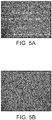
FIG. 5A depicts the transfer of ink lines to tape when ink lines were printed onto an uncoated glass substrate. -
FIG. 5B depicts the lack of transfer of ink lines to tape when the ink lines were printed onto an interlayer coated glass substrate in accordance with the present disclosure and as described in the examples. - The present disclosure provides compositions, which can be employed for any suitable or desired application including, for example, printable sensors or other electronic circuit devices. More particularly, the present disclosure provides a composition, which may be used to form an interlayer between substrates and printed conducted layers, constructed from various conductive compositions, such as metal ink compositions, e.g., XEROX® silver nanoparticle inks. The present composition can dramatically improve the adhesion between the substrates and conductive layers. Furthermore, devices incorporating the present composition exhibit surprisingly improved conductivity. Accordingly, the interlayer formed from the present compositions has surprisingly excellent insulative properties. Moreover, the present compositions do not require costly materials that are commercially difficult to obtain in large supply, such as polyvinyl phenol.
- In some embodiments, the present interlayer composition comprises a mixture of a polyvinyl butyral, a poly(melamine-co-formaldehyde) based polymer and an anhydride as described herein. The instant compositions may also optionally include an epoxy resin, a surface additive to control wetting and spreading properties of the present compositions and/or a catalyst to enhance the curing process of the composition deposited on a substrate. In some embodiments, the present interlayer compositions do not contain polyvinyl phenol.
- As used herein, "polyvinyl butyral", refers to a product obtained from the hydrolysis of polyvinyl acetate to form polyvinyl alcohol or a polyvinyl alcohol polymer containing residual vinyl acetate groups; the resulting polyvinyl alcohol product being reacted with butyraldehyde under acidic conditions to form a polyvinyl butyral containing various amounts of acetate, alcohol and butyraldehyde ketal groups. In some embodiments, the polyvinyl butyral is in the form of a powder or a pellet. Methods of preparing polyvinyl butyral are known in the art and are described for example in
U.S. Patent Publication No. 2012/0043512 , which is herein incorporated by reference in its entirety. - Polyvinyl butyral for use in the present composition may be represented by the following formula:

- In some embodiments, A is independently about 70 weight percent to about 95 weight percent, about 75 weight percent to about 90 weight percent, or about 80 weight percent to about 88 weight percent; B is independently about 5 weight percent to about 25 weight percent, about 7 weight percent to about 20 weight percent or about 11 weight percent to about 18 weight percent, such as about 17.5 weight percent; C is independently about 0 weight percent to about 10 weight percent, about 0 weight percent to about 5 weight percent or about 0 weight percent to about 3 weight percent, such as about 2.5 weight percent.
- In some embodiments, the polyvinyl butyral of Formula 1 has an average molecular weight (Mn) of about 10,000 to about 300,000 Daltons (Da), about 40,000 to about 200,000 Da or about 25,000 to about 150,000 Da. A representative composition of the polyvinyl butyral constitutes, on a weight basis, about 11% to 25% hydroxyl groups, calculated as polyvinyl alcohol, about 0% to about 2.5% acetate groups calculated as polyvinylacetate, with the balance being vinyl butyral groups, for example, about 80 wt.% to about 88 wt.%.
- Suitable polyvinyl butyral for use with the present interlayer compositions are commercially available and include, for example, BUTVAR® B-79 (available from Monsanto Chemical Co., St. Louis, MO) having a polyvinyl butyral content of about 88 wt.%., a polyvinyl alcohol content of about 11.0 wt.% to about 13.5 wt.%. and a polyvinyl acetate content of less than about 2.5 wt.%., wherein the average molecular weight of BUTVAR® B-79 is from about 50,000 to about 80,000 Da. More typically, BUTVAR® B-76 (Monsanto Chemical Co.) is used in the present interlayer composition. BUTVAR® B-76 has a polyvinyl butyral content of about 88% by weight, a polyvinyl alcohol content of about 11.5 wt.% to about 13.5 wt.% and a polyvinyl acetate content of less than about 2.5 wt.%, with an average molecular weight of about 90,000 to about 120,000 Da.
- The polyvinyl butyral can be provided in the composition in any suitable or desired amount. The amount of the polyvinyl butyral present in the instant interlayer in accordance with the present disclosure ranges from about 1 wt.% to about 20 wt.%, including from about 1 wt.% to about 10 wt.%, and from about 1 wt.% to about 5 wt.%, based on the total weight of solid in the instant interlayer compositions.
- In some embodiments, the present composition further includes a cross-linking agent, such as a melamine-formaldehyde based polymer. As used herein, the term "melamine-formaldehyde based polymer" refers to polymers formed by a condensation reaction of melamine (1,3,5-triazine-2,4,6-triamine) with formaldehyde (CH2O). In some embodiments, the free hydroxyl groups of the polyvinyl butyral bond with the melamine-formaldehyde based polymer. Thus, the polyvinyl butyral may be substituted with or "cross-linked" by the melamine-formaldehyde based polymer.
- Any suitable or desired melamine-formaldehyde based polymer may be included in the present composition. In some embodiments, the poly(melamine-co-formaldehyde) based polymer is represented by the following chemical structure:

- In another embodiment, the melamine-formaldehyde based polymer is an acrylated melamine-formaldehyde based polymer, represented by the following Formula III, wherein "m" is the number of repeats of the poly(melamine-co-formaldehyde), such as between 1 and 10, and R is H, CH3 or C4H9.

- Acrylated melamine-formaldehyde based polymers are commercially available from Sigma-Aldrich, Inc., for example, and may have a molecular weight between about 390 grams/mole and about 1,500 grams/mole.
- In some embodiments, the poly(melamine-co-formaldehyde) based polymer is selected from the group consisting of methylated poly(melamine-co-formaldehyde), butylated poly(melamine-co-formaldehyde), isobutylated poly(melamine-co-formaldehyde), acrylated poly(melamine-co-formaldehyde), methylated/butylated poly(melamine-co-formaldehyde), and combinations thereof.
- The poly(melamine-co-formaldehyde) based polymer can be provided in the interlayer composition in any suitable or desired amount. In some embodiments, the poly(melamine-co-formaldehyde) polymer is present in an amount of from about 0.5 percent to about 15 percent, or from about 1 percent to about 10 percent, or from about 1 percent to about 5 percent, by weight, based on the total weight of the interlayer composition.
- In some embodiments, the present composition further includes an anhydride, such as an acid anhydride. In certain embodiments, the anhydride functions as a catalyst/accelerator to enhance the curing process. In other embodiments, the anhydrides of the present disclosure may become covalently incorporated into the cured resin composition.
- Any suitable or desired anhydride can be selected for embodiments herein. Typical anhydrides include acetic anhydride, phthalic anhydride, fluorophthalic anhydride and unsaturated dicarboxylic acid anhydride. Examples of suitable unsaturated dicarbo anhydride include maleic anhydride, citraconic anhydride, itaconic anhydride and aconitic anhydride.
- One or more anhydrides can be provided in the composition in any suitable or desired amount. In some embodiments, anhydride is present in an amount of from about 0.01 to about 10 percent, or from about 0.1 percent to about 5 percent, or from about 0.1 percent to about 3 percent, by weight, based on the total weight of the interlayer composition. Suitable acid anhydrides are commercially available and may be obtained from Sigma-Aldrich Inc., for example.
- In some embodiments, the present composition, optionally, further includes epoxy resins. The epoxy resin component may be any type of epoxy resin, including any material containing one or more reactive oxirane groups (also termed epoxy groups) as shown below.

- Epoxy resins useful in embodiments disclosed herein may include aromatic, aliphatic or heterocyclic epoxy resins. The epoxies may be pure compounds or mixtures of compounds containing one, two or more epoxy groups per molecule. In some embodiments, epoxy resins may also include reactive -OH groups, which may react with the anhydrides, for example, to result in additional crosslinking at higher temperatures, such as the curing temperatures described herein.
- In some embodiments, the present compositions include glycidyl epoxy resins, such as glycidyl-ether epoxy resins, glycidyl-amine epoxy resins and glycidyl-ester epoxy resins. Glycidyl epoxy resins are commercially available or may be prepared via a condensation reaction of an appropriate dihydroxy compound and epichlorohydrin as is known in the art.
- In some embodiments, the present compositions include non-glycidyl epoxy resins, such as cycloaliphatic epoxy resins. Non-glycidyl epoxies are commercially available or may be formed by peroxidation of an olefinic double bond as known in the art.
- Suitable epoxy resins include those having aromatic moieties. Representative glycidyl-ether epoxy resins having aromatic moieties include diglycidyl ethers of bisphenol-A (DGEBA) which is synthesized by reacting bisphenol-A with epichlorohydrin in the presence of a basic catalyst and which has the following structure.

- Typically, x, the number of repeating units, ranges from 0 to 25.
- DGEBA resins are commercially available and are marketed under the trade designations EPON™ 828, EPON™ 1001, EPON™ 1004, EPON™ 2004, EPON™ 1510, and EPON™ 1310 from Hexion, Inc., Columbus, OH and D.E.R.™ 331, D.E.R. ™ 332, D.E.R.™ 334, and D.E.R.™ 439, available from Dow Chemical Co., Midland, MI.
- Other suitable bisphenol-A epoxy resins include Bisphenol A propoxylate diglycidyl ether, which is also commercially available, e.g., from Sigma-Aldrich, Inc. and which has the following structure:

- Other suitable glycidyl ether epoxy resins comprising aromatic moieties include bis(4-hydroxyphenyl)methane (known as bisphenol F) and diglycidyl ether of bromobisphenol A (2,2-bis(4-(2,3-epoxypropoxy)3-bromo-phenyl)propane). Bisphenol-F based epoxy resins are commercially available, e.g., D.E.R. ™ 354 and D.E.R. ™ 354LV, each available from The Dow Chemical Company, Midland, Michigan.
- Additional glycidyl ether epoxy resins comprising aromatic moieties that may be used with the instant compositions include phenol and cresol novolacs. As is known in the art, these epoxies may be prepared by reacting phenols or cresols, in excess, with formaldehyde in the presence of an acidic catalyst to produce phenolic novolac resin. Novolac epoxy resins are then synthesized by reacting the phenolic novolac resin with epichlorohydrin in the presence of sodium hydroxide as a catalyst. A representative phenol novalac is depicted below, wherein "n" is a number of repeat units, such as from 0 to 5.

- Examples of epoxy phenolic novolac resins including epoxy bisphenol A novolac resins useful in some embodiments disclosed herein include those available under the tradenames D.E.N. ™ 431 and D.E.N. ™ 438 from The Dow Chemical Company, Midland, Michigan, and EPON™ SU-8, available from Hexion Specialty Chemicals, Columbus, OH.
- Other suitable epoxy resins containing aromatic groups include those that can be prepared by the reaction of aromatic alcohols such as biphenyl diols and triphenyl diols and triols with epichlorohydrin. One representative compound is tris-(hydroxyl phenyl)methane-based epoxy available from Huntsman Corporation, Basel, Switzerland as Tactix™ 742.
- Additional suitable expoxy resins include glycidal amines. Glycidal amines are formed by reacting epichlorohydrin with an amine, such as an aromatic amine. An example of a suitable glycidal amine is tetraglycidyl methylene dianiline, which is represented by the following structure:

- Additional suitable epoxy resins include aliphatic epoxy resins. Aliphatic epoxy resins are known in the art and include glycidyl epoxy resins and cycloaliphatic epoxides. Glycidyl aliphatic epoxy resins are typically formed by the reaction of epichlorohydrin with aliphatic alcohols or polyols to give glycidyl ethers or aliphatic carboxylic acids to give glycidyl esters. This reaction is normally done in the presence of an alkali, such as sodium hydroxide, to facilitate the dehydrochlorination of the intermediate chlorohydrin. These resins generally display low viscosity at room temperature (10-200 mPa.s). Typical glycidyl aliphatic epoxy resins for use in the present interlayer composition include trimethylolpropane triglycidyl ether, neopentyl glycol diglycidyltEther and poly(propylene glycol) diglycidyl ether, which are commercially available, for example, from Sigma-Aldrich, Inc.
- Cycloaliphatic epoxides may also be included in the present compositions. Cycloaliphatic epoxides contain one or more cycloaliphatic rings in the molecule to which an epoxide ring is fused. They are formed by the reaction of cyclo-olefins with a peracid, such as peracetic acid. Cycloaliphatic epoxides suitable for use in preparing the instant composition include 3,4-epoxycyclohexylmethyl-3,4-epoxycyclohexane carboxylate, bis(3,4-epoxycyclohexylmethyl)adipate, vinyl cyclohexane dioxide and the like and are commercially available from, for example, Union Carbide Corporation, a subsidiary of the Dow Chemical Company, Houston, TX.
- One or more epoxy resins can be provided in the composition of the disclosure in any suitable or desired amount. In embodiments, epoxy resin is present in an amount of from about 0 to about 40 percent, or from about 5 to about 35 percent, or from about 10 to about 25 percent, by weight, based on the total weight of the present composition.
- Any suitable or desired surfactant can be included in the present interlayer compositions. In embodiments, the surfactant is selected from the group consisting of a silicone modified polyacrylate, a polyester modified polydimethylsiloxane, a polyether modified polydimethylsiloxane, a polyacrylate modified polydimethylsiloxane, a polyester polyether modified polydimethylsiloxane, a low molecular weight ethoxylated polydimethylsiloxane, polyether modified polydimethylsiloxane, polyester modified polymethylalkylsiloxane, polyether modified polymethylalkylsiloxane, aralkyl modified polymethylalkylsiloxane, polyether modified polymethylalkylsiloxane, polyether modified polydimethylsiloxane and combinations thereof.
- For example, the surfactant may be a polysiloxane copolymer that includes a polyester modified polydimethylsiloxane, commercially available from BYK-Chemie GmbH, Wesel, Germany with the trade name of BYK® 310; a polyether modified polydimethylsiloxane, commercially available from BYK-Chemie GmbH with the trade name of BYK® 330; a polyacrylate modified polydimethylsiloxane, commercially available from BYK Chemical with the trade name of BYK®-SILCLEAN 3700 (about 25 weight percent in methoxypropylacetate); or a polyester polyether modified polydimethylsiloxane, commercially available from BYK-Chemie GmbH with the trade name of BYK® 375. The surfactant can also be a low molecular weight ethoxylated polydimethylsiloxane with the trade name SILSURF® A008 available from Siltech Corporation, Ontario, Canada. Some other examples of suitable surfactants include BYK® 3500, BYK® 3510, BYK® 307, BYK® 333, BYK® ANTI-TERRA-U100, BYK® A-004, BYK® C-409.
- One or more surfactants can be provided in the composition of the disclosure in any suitable or desired amount. In some embodiments, the surfactant is present in an amount of from about 0.01 to about 5 percent, from about 0.1 to about 3.5 percent, or from about 0.5 to about 2 percent, by weight, based on the total weight of the present composition.
- The composition of the present disclosure can optionally comprise a catalyst to enhance the curing process. Any suitable or desired catalyst can be selected for use in the present compositions. In embodiments, the catalyst is selected from the group consisting of amine salts of dodecylbenzene sulfonic acid (DDBSA), para toluene sulfonic acid, triflouromethane sulfonic acid, and combinations thereof.
- One or more catalysts can be provided in the present composition in any suitable or desired amount. In embodiments, the catalyst is present in an amount of from about 0.05 to about 1.5 percent, or from about 0.08 to about 1.0 percent, or from about 0.1 to about 0.5 percent, by weight, based on the total weight of the instant composition.
- Any suitable or desired solvent can be selected for the present interlayer compositions. In some embodiments, the solvent is selected from the group consisting of propylene glycol methyl ether acetate, toluene, methyl isobutyl ketone, butylacetate, methoxypropylacetate, xylene, tripropyleneglycol monomethylether, dipropyleneglycol monomethylether, propoxylated neopentylglycoldiacrylate, and combinations thereof.
- One or more solvents can be included in the present composition in any suitable or desired amount. In some embodiments, the solvent is present in an amount of from about 50 to about 90 percent or from about 60 to about 80 percent or from about 70 to about 80 percent, by weight, based on the total weight of the composition in accordance with the present disclosure.
- In some embodiments, the present composition comprises from about 10 to about 50 weight percent solids, or from about 15 to about 40 weight percent solids, or from about 20 to about 30 weight percent solids, based on the total weight of the composition in accordance with the present disclosure. In specific embodiments, the present composition contains a selected solids content of less than about 30 weight percent solids, based on the total weight of the instant composition. For example, in some embodiments, the present composition contains a solids content of from about 10 to less than about 30 weight percent solids, or from about 15 to less than about 30 weight percent solids, or from about 20 to less than about 30 weight percent solids, based on the total weight of the composition in accordance with the present disclosure.
- The instant disclosure is also directed to a device including a substrate, an interlayer disposed thereover, and a conductive composition disposed over the interlayer. The substrate may be any suitable substrate including silicon, a glass plate, a plastic film, sheet, fabric, or synthetic paper. For structurally flexible devices, plastic substrates such as polyester, polycarbonate, polyimide sheets, polyethylene terephthalate (PET) sheet, polyethylene naphthalate (PEN) sheet, and the like, may be used. The thickness of the substrate can be any suitable thickness, such as about 10 micrometers to over 10 millimeters with an exemplary thickness being from about 50 micrometers to about 2 millimeters, especially for a flexible plastic substrate, and from about 0.4 to about 10 millimeters for a rigid substrate such as glass or silicon.
- The interlayer of the present device is formed from a composition in accordance with the present disclosure comprising a polyvinyl butyral resin; a melamine resin, such as a poly(melamine-co-formaldehyde) based polymer; an anhydride, an optional epoxy resin; an optional surfactant; and an optional catalyst.
- The interlayer may be disposed on the substrate using any suitable method. For example, the present composition may be disposed on the substrate by solution depositing. Solution depositing as used herein refers to a process whereby a liquid is deposited upon the substrate to form a coating or layer. Solution depositing includes, for example, one or more of spin coating, dip coating, spray coating, slot die coating, flexographic printing, offset printing, screen printing, gravure printing or ink jet printing the interlayer composition onto the substrate.
- In some embodiments, the interlayer is a film. The film formed from the instant composition may be present on the substrate at any suitable or desired thickness. In some embodiments, the dried film thickness of the interlayer is from about 0.2 to about 5 micrometers, or from about 0.5 to about 3 micrometers, or from about 0.75 to about 1 micrometers. In a specific embodiment, the coating thickness of the interlayer is from about 0.2 to about 1 micrometer. Typically, the film formed from the compositions of the disclosure does not contain polyvinyl phenol.
- In some embodiments, the interlayer, which is disposed on the substrate, is cured. The interlayer can be cured at any suitable or desired temperature for any suitable period of time. In some embodiments, the interlayer disposed on the substrate can be cured at a temperature of from about 80 °C to about 200 °C, or from about 100 °C to about 180 °C, or from about 120 °C to about 160 °C for a period of from about 0.5 to about 6 hours, or from about 1 to about 4 hours, or from about 2 to about 3 hours. In embodiments, the present composition can be cured at about 160 °C for about 6 hours or at about 200 °C for about 0.5 hours.
- In some embodiments, the resulting interlayer, after curing, provides a film having balanced properties for printing electronics including a suitable water contact angle for controlling ink wettability, surface smoothness, suitable glass transition for controlling the flexibility for flexible electronics fabrications, electrical insulating properties and other properties as described herein. In some embodiments, the cured film possesses a water contact angle of from about 65 degrees to about 95 degrees. In some embodiments, the thermally cured film possesses a surface roughness of from about 1 nanometer to about 10 nanometers. In embodiments, the cured film has a glass transition temperature of from about minus 10 °C to about 100 °C.
- In some embodiments, the device includes a conductive material. Any suitable or desired conductive material can be used to form conductive features on the present device. Typically, a conductive composition, such as a metal ink composition, is used to provide the conductive features. Suitable metal ink compositions are described in
U. S. Patent 8,324,294 andU. S. Patent Publication 2014/0312284 , which are each herein incorporated by reference in their entireties, and which include, for example, silver nanoparticles dispersed within an ink vehicle, such as aromatic hydrocarbons including benzene, toluene, xylene and ethylbenzene. The fabrication of conductive features, such as an electrically conductive element, from a metal ink composition, for example, from a nanoparticle metal ink, such as a nanosilver ink composition, can be carried out by depositing the nanosilver ink composition, for example, onto a substrate using any suitable deposition technique including solution processing as described herein at any suitable time prior to or subsequent to the formation of other layers on the substrate. Thus, deposition of the nanosilver ink composition, for example, onto the substrate can occur either on a substrate or on a substrate already containing layered material, for example, a substrate having disposed thereon the composition in accordance with the present disclosure. - In some embodiments, the conductive features are formed by heating the conductive composition. In some embodiments, prior to heating, the layer of the deposited conductive composition may be electrically insulating or may have very low electrical conductivity; however, heating results in an electrically conductive layer composed of annealed metal particles, for example, such as annealed silver nanoparticles, which increases the conductivity. In some embodiments, the annealed silver nanoparticles, for example, may be coalesced or partially coalesced silver nanoparticles. In other embodiments, it may be possible that in the annealed metal nanoparticles, for example, the silver nanoparticles, achieve sufficient particle-to-particle contact to form the electrically conductive layer without coalescence.
- The deposited conductive composition, such as a metal ink composition, is heated to any suitable or desired temperature, such as from about 70 °C to about 250 °C, or any temperature sufficient to induce annealing of the metal particles, for example, and thus form an electrically conductive layer, which is suitable for use as an electrically conductive element in electronic devices. The heating temperature is one that does not cause adverse changes in the properties of previously deposited layers or the substrate. In some embodiments, use of low heating temperatures allows use of low cost plastic substrates, which have an annealing temperature of below 140 °C.
- The heating can be for any suitable or desired time, such as from about 0.01 hours to about 10 hours. The heating can be performed in air, in an inert atmosphere, for example under nitrogen or argon, or in a reducing atmosphere, for example, under nitrogen containing from about 1 to about 20 percent by volume hydrogen. The heating can also be performed under normal atmospheric pressure or at a reduced pressure of, for example, about 1000 mbars to about 0.01 mbars.
- Heating encompasses any technique that can impart sufficient energy to the heated material or substrate to anneal the metal nanoparticles, for example. These techniques include thermal heating (for example, at hot plate, an oven, and a burner), infra-red ("IR") radiation, laser beam, flash light, microwave radiation, or ultraviolet ("UV") radiation, or a combination thereof.
- In some embodiments, after heating, an electrically conductive line, such as an electrically conductive silver line, is formed on the substrate that has a thickness ranging from about 0.1 to about 20 micrometers, or from about 0.15 to about 10 micrometers. In certain embodiments, after heating, the resulting electrically conductive line has a thickness of from about 0.1 to about 2 micrometers.
- The conductivity of the conductive features, such as an electrically conductive line, which is produced by heating the deposited conductive composition is more than about 10,000 Siemens/centimeter (S/cm), more than about 50,000 S/cm, more than about 80,000 S/cm, more than about 100,000 S/cm, more than about 125,000 S/cm, more than about 150,000 S/cm or more than about 200,000 S/cm. Typically, the conductivity ranges from about 50,000 S/cm to about 200,000 S/cm, such as about 80,000 S/cm to about 150,000 S/cm, such as about 100,000 S/cm to about 125,000 S/cm.
- The resistivity of the conductive features, such as an electrically conductive line, which is produced by heating the deposited conductive composition is less than about 1.0 x 10⁻⁴ ohms-centimeter (ohms-cm), less than about 2.0 x 10⁻⁵ ohms-cm, less than about 1.25 x 10⁻⁵ ohms-cm, less than about 1.0 x 10⁻⁵ ohms-cm, less than about 8.0 x 10⁻⁶ ohms-cm, less than about 6.6 x 10⁻⁶ ohms-cm or less than about 5.0 x 10⁻⁶ ohms-cm. Typically, the resistance ranges from about 2.0 x 10⁻⁵ ohms-cm to about 5.0 x 10⁻⁶ ohms-cm, such as about 1.25 x 10⁻⁵ ohms-cm to about 6.6 x 10⁻⁶ ohms-cm, such as about 1.0 x 10⁻⁵ ohms-cm to about 8.0 x 10⁻⁶ ohms-cm.
- The device of the present disclosure may be used for any suitable or desired application, such as for electrodes, conductive pads, interconnects, conductive lines, conductive tracks, and the like, in electronic devices such as thin film transistors, organic light emitting diodes, printed antenna, and other electronic devices requiring conductive elements or components.
- Also provided herein is a cured film formed from a composition comprising a polyvinyl butyral represented by Formula I, a poly(melamine-co-formaldehyde) based polymer and an anhydride as described herein. Typically, the cured film is formed from the composition in accordance with the present disclosure that does not contain polyvinyl phenol.
- In some embodiments, the cured film comprises conductive features, such as an electrically conductive line, as described herein. Typically, the conductivity of the conductive features of the cured film is more than about 10,000 Siemens/centimeter (S/cm), more than about 50,000 S/cm, more than about 80,000 S/cm, more than about 100,000 S/cm, more than about 125,000 S/cm, more than about 150,000 S/cm or more than about 200,000 S/cm. More typically, the conductivity of the cured film comprising the conductive features, such as an electrically conductive line, ranges from about 50,000 S/cm to about 200,000 S/cm, such as about 80,000 S/cm to about 150,000 S/cm, such as about 100,000 S/cm to about 125,000 S/cm.
- In some embodiments, the resistivity of the conductive features, such as an electrically conductive line of the cured film is less than about 1.0 x 10⁻⁴ ohms-centimeter (ohms-cm), less than about 2.0 x 10⁻⁵ ohms-cm, less than about 1.25 x 10⁻⁵ ohms-cm, less than about 1.0 x 10⁻⁵ ohms-cm, less than about 8.0 x 10⁻⁶ ohms-cm, less than about 6.6 x 10⁻⁶ ohms-cm or less than about 5.0 x 10⁻⁶ ohms-cm. Typically, the resistivity of the cured film comprising the conductive features, such as an electrically conductive line, ranges from about 2.0 x 10⁻⁵ ohms-cm to about 5.0 x 10⁻⁶ ohms-cm, such as about 1.25 x 10⁻⁵ ohms-cm to about 6.6 x 10⁻⁶ ohms-cm, such as about 1.0 x 10⁻⁵ ohms-cm to about 8.0 x 10⁻⁶ ohms-cm.
- Also provided herein is a process for forming conductive features, such as an electrically conductive line as described herein, on a substrate including depositing an interlayer composition onto a substrate as described herein; curing the interlayer to form an interlayer film; depositing a conductive composition, such as a metal ink composition, onto the interlayer film to form deposited features; and heating the deposited features to form the conductive features as described herein. The conductive features can be fabricated by any suitable or desired method. In embodiments, the conductive features can be prepared by solution processing techniques such as ink jet printing on the substrates with a pre-applied interlayer. The conductive features show high conductivity with significantly improved adhesion after annealing at a suitable temperature.
- The following Examples are being submitted to further define various species of the present disclosure. These Examples are intended to be illustrative only and are not intended to limit the scope of the present disclosure. Also, parts and percentages are by weight unless otherwise indicated.
- Interlayer composition Samples 1-3 were prepared using the components and amounts shown in Table 1. The interlayer components were prepared as follows. A 20% solution of poly(propylene glycol) diglycidyl ether (PLGDE) was prepared by mixing 20 grams of poly(propylene glycol) diglycidyl ether and 80 grams of propylene glycol monomethyl ether acetate (PGMEA) solvent in a glass bottle. A 10% polyvinyl butyral (PVB) solution was prepared by the slow addition of 10 grams polyvinyl butyral powder (PVB BUTVAR®-76) into 90 grams PGMEA solvent in a glass bottle, followed by mixing until the polyvinyl butyral powder was completely dissolved. Methylated poly(melamine co-formaldehyde) 84 weight percent solution in 1-butanol (PMMF) was obtained from Sigma-Aldrich, Inc. The average Mn of the methylated poly(melamine co-formaldehyde) was -432 Da.
- Sample 1 was prepared by adding 2.5 grams of PLGDE into a vial, followed by the addition of 2 grams of PVB, 0.06 grams of PMMF and 0.1 grams acetic anhydride. The vial was placed on a vortex at a speed of 2000 revolutions per minute (rpm) for 10 seconds.
- Sample 2 was prepared by adding 0.1 grams of acetic anhydride into a vial, followed by the addition of 2 grams of PGMEA, 2.0 grams of PVB and 0.2 grams of PMMF. The vial was placed on a vortex at a speed of 2000 rpm for 10 seconds.
-
Sample 3 was prepared by adding 5 grams of PLGDE into a vial, followed by the addition of 2 grams of PVB and 0.2 grams of PMMF and 0.2 grams of acetic anyhydride. The vial was placed on a vortex at a speed of 2000 rpm for 10 seconds. - Samples 1-3 were each coated onto pre-cleaned microscope glass or polyethylene naphthalate (PEN) substrate using an SCS P6700 Spin-coater (Specialty Coating Systems, Inc., Indianapolis, Indiana). The coating speed was initially set at 100 rpm for 5 seconds and then increased up to 1600 rpm for 60 seconds. The formulations were pre-heated at 100 °C for 10 minutes, and then cured at temperatures from 160 °C to 200 °C. Curing conditions for each of the formulations on glass or PEN substrates is described in Table 2, below.
- A silver nanoparticle ink was prepared as described in
U. S. Patent Publication 2014/0312284 , which is hereby incorporated by reference in its entirety. Briefly, the silver nanoparticle ink composition was prepared by mixing silver nanoparticle powders with a solvent mixture of bicyclohexane and phenylcyclohexane at a 3:2 ratio. The silver nanoparticles were 50 weight percent of the composition. After the silver nanoparticles were mixed into the solvents, the composition was filtered using a 1.0 µm syringe filter. - The silver nanoparticle ink described above was printed using a Dimatix DMP2800 (Fujifilm Diamtix, Inc., Lebanon, New Hampshire) equipped with 10 picoliter (pL) cartridge. All nozzles worked perfectly, forming spherical drops. Line widths of about 70-80 microns were printed onto uncoated and interlayer coated glass or PEN substrates. Curing was performed as described in Table 2, below. When printed on uncoated and interlayer coated glass, as shown in
Figure 1A (uncoated glass),Figure 1B (interlayer coated glass, Sample 1),Figure 2A (uncoated glass),Figure 2B (coated glass, Sample 2),Figure 4A (uncoated glass) andFigure 4B (interlayer coated glass, Sample 3) or uncoated and interlayer coated PEN, as shown inFigure 3A (uncoated PEN) andFigure 3B (interlayer coated PEN, Sample 2), straight lines with uniform edges were obtained. No deformation in line shape was observed upon thermal sintering. All printed lines were highly conductive after annealing at about 120 °C for about 30 minutes. - After printing and annealing at 120 °C for 30 minutes, the printed lines were subjected to an adhesion test by sticking SCOTCH® Magic™ Tape (3M) to the surface of the conductive lines, and then peeling the SCOTCH® Magic™ tape off of the surface. The peeled tape was attached to XEROX® 4200 paper. When no interlayer was used, the adhesion was very poor and a large amount of ink lines were peeled off as shown in
Figure 5A . In contrast, glass or PEN substrates, which were coated with any of interlayer Samples 1-3, demonstrated excellent adhesion. As shown inFigure 5B , none of the silver ink lines were peeled off of glass coated with an interlayer composition prepared according to the present disclosure. - The conductivity was calculated based on the resistivity measurement. Resistivity = ohms X height X width / length, Conductivity = 1/resistivity. The resistance of the printed line was measured using Keithley SCS-4200 (Tektronix, Inc., Beverton, Oregon). Step height and width of the printed line were measured using a Bruker DektakXT Surface Profilometer.
- The results, summarized in Table 2, below, show the higher conductivity printed on a surface comprising an interlayer of the present disclosure, in comparison to the conductivity on a bare glass substrate.
Table 2: Summary of Resistivity and Conductivity Sample ID Substrates Curing Condition Conductivity S/cm No coating Glass N/A 9.34E + 04 Sample 1 Glass 200°C-1.5 hours 9.51E +04 Sample 2 Glass 200°C-1.5 hours 1.19E + 05 Sample 2 PEN 160°C-16 hours 1.10E+05 Sample 3Glass 200°C-1.5 hours 1.18E + 05
| Sample ID | PLGDE a | PMMF b | PVB-76 c | Acetic Anhydride | Solid (%) | PGMEA d | Total Weight |
| 1 | 10.73 | 1.29 | 4.29 | 2.15 | 18.45 | 81.55 | 4.7 |
| 2 | 4.65 | 4.65 | 2.31 | 11.61 | 88.39 | 4.3 | |
| 3 | 13.51 | 2.70 | 2.70 | 2.70 | 21.62 | 78.38 | 7.4 |
| a poly(propylene glycol) diglycidyl ether b Poly(melamine-co-formaldehyde) methylated c 10% polyvinyl butyral d propylene glycol monomethyl ether acetate |
Claims (10)
- A composition comprising a polyvinyl butyral represented by the following formula:

a poly(melamine-co-formaldehyde) based polymer and
an anhydride. - The composition of claim 1, wherein A is independently from about 80 weight percent to about 88 weight percent; B is independently from about 11 weight percent to about 18 weight percent; and C is independently from about 0 weight percent to about 3 weight percent.
- The composition according to claim 1, wherein an average molecular weight of the polyvinyl butyral ranges from about 25,000 Daltons to about 150,000 Daltons.
- The composition according to claim 1, wherein the poly(melamine-co-formaldehyde) based polymer is selected from the group consisting of a methylated poly(melamine-co-formaldehyde) polymer, a butylated poly(melamine-co-formaldehyde) polymer, an isobutylated poly(melamine-co-formaldehyde) polymer, an acrylated poly(melamine-co-formaldehyde) polymer and a methylated/butylated poly(melamine-co-formaldehyde) polymer.
- A device comprising: a substrate; an interlayer; and conductive features,
wherein the interlayer comprises a thermally cured film formed from a composition comprising:a polyvinyl butyral represented by the following formula: a poly(melamine-co-formaldehyde) based polymer andan anhydride.
 - The device of claim 5, wherein A is independently from about 80 weight percent to about 88 weight percent; B is independently from about 11 weight percent to about 18 weight percent; and C is independently from about 0 weight percent to about 3 weight percent.
- The device of claim 5, wherein the substrate is selected from the group consisting of a polyethylene naphthalate substrate and a glass substrate.
- The device of claim 5, wherein the conductive features comprise an electrically conductive element formed from a nanoparticle conductive ink composition.
- A cured film formed from a composition comprising a polyvinyl butyral represented by the following formula:

a poly(melamine-co-formaldehyde) based polymer and
an anhydride,
wherein the cured film comprises conductive features. - The cured film of claim 9, wherein a conductivity of the cured film ranges from about 50,000 S/cm to about 200,000 S/cm.
Applications Claiming Priority (1)
| Application Number | Priority Date | Filing Date | Title |
|---|---|---|---|
| US15/164,669 US10208224B2 (en) | 2016-06-13 | 2016-06-13 | Interlayer composition for electronic printing |
Publications (2)
| Publication Number | Publication Date |
|---|---|
| EP3257906A1 true EP3257906A1 (en) | 2017-12-20 |
| EP3257906B1 EP3257906B1 (en) | 2020-08-05 |
Family
ID=58772484
Family Applications (1)
| Application Number | Title | Priority Date | Filing Date |
|---|---|---|---|
| EP17172581.5A Active EP3257906B1 (en) | 2016-06-13 | 2017-05-23 | Interlayer composition for electronic printing |
Country Status (3)
| Country | Link |
|---|---|
| US (1) | US10208224B2 (en) |
| EP (1) | EP3257906B1 (en) |
| CN (1) | CN107488321B (en) |
Families Citing this family (6)
| Publication number | Priority date | Publication date | Assignee | Title |
|---|---|---|---|---|
| US10843262B2 (en) | 2018-08-02 | 2020-11-24 | Xerox Corporation | Compositions comprising eutectic metal alloy nanoparticles |
| US10947424B2 (en) | 2018-08-02 | 2021-03-16 | Xerox Corporation | Adhesive composition comprising eutectic metal alloy nanoparticles |
| US11142671B2 (en) * | 2018-08-02 | 2021-10-12 | Xerox Corporation | Adhesive composition comprising metal nanoparticles |
| US10800948B2 (en) | 2018-08-02 | 2020-10-13 | Xerox Corporation | Conductive adhesive compositions and method for the same |
| US10577515B1 (en) | 2018-10-02 | 2020-03-03 | Xerox Corporation | Dielectric ink composition |
| EP4288229A1 (en) | 2021-02-03 | 2023-12-13 | Basf Se | Compositions, comprising silver nanoplatelets |
Citations (5)
| Publication number | Priority date | Publication date | Assignee | Title |
|---|---|---|---|---|
| US20120043512A1 (en) | 2010-08-20 | 2012-02-23 | Xerox Corporation | Silver nanoparticle ink composition for highly conductive features with enhanced mechanical properties |
| US8324294B2 (en) | 2011-03-07 | 2012-12-04 | Xerox Corporation | Solvent-based inks comprising silver nanoparticles |
| US20140312284A1 (en) | 2013-04-19 | 2014-10-23 | Xerox Corporation | Conductive ink compositions and methods for preparation of stabilized metal-containing nanoparticles |
| US20140374672A1 (en) * | 2013-06-24 | 2014-12-25 | Xerox Corporation | Conductive metal inks with polyvinylbutyral binder |
| CN103589269B (en) * | 2013-10-12 | 2016-04-20 | 安徽自动化仪表有限公司 | A kind of anti-oxidant heat radiation coating for meter housing and preparation method thereof |
Family Cites Families (6)
| Publication number | Priority date | Publication date | Assignee | Title |
|---|---|---|---|---|
| US2732325A (en) * | 1950-01-25 | 1956-01-24 | Modified diaminotriazine-aldehyde | |
| US3226256A (en) * | 1963-01-02 | 1965-12-28 | Jr Frederick W Schneble | Method of making printed circuits |
| US5118657A (en) * | 1988-09-30 | 1992-06-02 | Matsushita Electric Industrial Co., Ltd. | Dye transfer type thermal printing sheets |
| US6894123B2 (en) * | 2003-03-21 | 2005-05-17 | E.I. Du Pont De Nemours And Company | Acetoacetylated polyvinyl polymers and curable coating compositions made therefrom |
| US8426749B2 (en) * | 2007-05-09 | 2013-04-23 | Fujifilm Corporation | Electromagnetic shielding film and optical filter |
| US20170233541A1 (en) * | 2016-02-12 | 2017-08-17 | Tyco Electronics Corporation | Method of Enhancing Adhesion of Silver Nanoparticle Inks on Plastic Substrates Using a Crosslinked Poly(vinyl butyral) Primer Layer |
-
2016
- 2016-06-13 US US15/164,669 patent/US10208224B2/en active Active
-
2017
- 2017-05-04 CN CN201710307510.7A patent/CN107488321B/en active Active
- 2017-05-23 EP EP17172581.5A patent/EP3257906B1/en active Active
Patent Citations (5)
| Publication number | Priority date | Publication date | Assignee | Title |
|---|---|---|---|---|
| US20120043512A1 (en) | 2010-08-20 | 2012-02-23 | Xerox Corporation | Silver nanoparticle ink composition for highly conductive features with enhanced mechanical properties |
| US8324294B2 (en) | 2011-03-07 | 2012-12-04 | Xerox Corporation | Solvent-based inks comprising silver nanoparticles |
| US20140312284A1 (en) | 2013-04-19 | 2014-10-23 | Xerox Corporation | Conductive ink compositions and methods for preparation of stabilized metal-containing nanoparticles |
| US20140374672A1 (en) * | 2013-06-24 | 2014-12-25 | Xerox Corporation | Conductive metal inks with polyvinylbutyral binder |
| CN103589269B (en) * | 2013-10-12 | 2016-04-20 | 安徽自动化仪表有限公司 | A kind of anti-oxidant heat radiation coating for meter housing and preparation method thereof |
Also Published As
| Publication number | Publication date |
|---|---|
| US10208224B2 (en) | 2019-02-19 |
| CN107488321B (en) | 2021-12-21 |
| US20170355871A1 (en) | 2017-12-14 |
| EP3257906B1 (en) | 2020-08-05 |
| CN107488321A (en) | 2017-12-19 |
Similar Documents
| Publication | Publication Date | Title |
|---|---|---|
| EP3257906B1 (en) | Interlayer composition for electronic printing | |
| US7285579B2 (en) | Solventless, non-polluting radiation curable coatings | |
| KR102590625B1 (en) | Resin composition | |
| JP7156267B2 (en) | Carboxylic acid group-containing polyester adhesive composition | |
| TWI551633B (en) | Metal stabilizers for epoxy resins | |
| JP7143259B2 (en) | Conductive adhesive composition and method | |
| US11345784B2 (en) | Resin composition, and resin film, metal foil with resin, metal clad laminate, wiring board, and circuit mount component using same | |
| US10947424B2 (en) | Adhesive composition comprising eutectic metal alloy nanoparticles | |
| US20170183536A1 (en) | Interlayer Composition For Electronic Printing | |
| US11142671B2 (en) | Adhesive composition comprising metal nanoparticles | |
| TWI519577B (en) | Metal stabilizers for epoxy resins and dispersion process | |
| TW201542758A (en) | Conductive composition and conductive molded article | |
| TW201035148A (en) | Metal stabilizers for epoxy resins and advancement process | |
| CN107298922B (en) | Interlayer composition and devices made therefrom | |
| TW201213455A (en) | Curable composition for inkjet and method for producing electronic component | |
| JP2967117B2 (en) | Electron beam-curable conductive paste composition | |
| US20090227719A1 (en) | Curable High Dielectric Constant Ink Composition and High Dielectric Film | |
| JP2023018665A (en) | Conductive resin composition | |
| JPH0575290A (en) | Manufacture of electromagnetic wave shielding board | |
| JP2012117055A (en) | Insulator ink resin composition, resist pattern, and resist pattern-forming method | |
| TW201316850A (en) | Epoxy resin composition and print substrate formed from using the same |
Legal Events
| Date | Code | Title | Description |
|---|---|---|---|
| PUAI | Public reference made under article 153(3) epc to a published international application that has entered the european phase |
Free format text: ORIGINAL CODE: 0009012 |
|
| STAA | Information on the status of an ep patent application or granted ep patent |
Free format text: STATUS: THE APPLICATION HAS BEEN PUBLISHED |
|
| AK | Designated contracting states |
Kind code of ref document: A1 Designated state(s): AL AT BE BG CH CY CZ DE DK EE ES FI FR GB GR HR HU IE IS IT LI LT LU LV MC MK MT NL NO PL PT RO RS SE SI SK SM TR |
|
| AX | Request for extension of the european patent |
Extension state: BA ME |
|
| STAA | Information on the status of an ep patent application or granted ep patent |
Free format text: STATUS: REQUEST FOR EXAMINATION WAS MADE |
|
| 17P | Request for examination filed |
Effective date: 20180620 |
|
| RBV | Designated contracting states (corrected) |
Designated state(s): AL AT BE BG CH CY CZ DE DK EE ES FI FR GB GR HR HU IE IS IT LI LT LU LV MC MK MT NL NO PL PT RO RS SE SI SK SM TR |
|
| STAA | Information on the status of an ep patent application or granted ep patent |
Free format text: STATUS: EXAMINATION IS IN PROGRESS |
|
| 17Q | First examination report despatched |
Effective date: 20181129 |
|
| GRAP | Despatch of communication of intention to grant a patent |
Free format text: ORIGINAL CODE: EPIDOSNIGR1 |
|
| STAA | Information on the status of an ep patent application or granted ep patent |
Free format text: STATUS: GRANT OF PATENT IS INTENDED |
|
| RIC1 | Information provided on ipc code assigned before grant |
Ipc: B32B 27/42 20060101ALI20200128BHEP Ipc: B32B 7/12 20060101ALI20200128BHEP Ipc: C09D 11/10 20140101AFI20200128BHEP Ipc: C09D 11/106 20140101ALI20200128BHEP Ipc: C08L 29/14 20060101ALI20200128BHEP Ipc: C09D 129/14 20060101ALI20200128BHEP Ipc: C09D 11/52 20140101ALI20200128BHEP Ipc: C09D 11/103 20140101ALI20200128BHEP |
|
| INTG | Intention to grant announced |
Effective date: 20200228 |
|
| GRAS | Grant fee paid |
Free format text: ORIGINAL CODE: EPIDOSNIGR3 |
|
| GRAA | (expected) grant |
Free format text: ORIGINAL CODE: 0009210 |
|
| STAA | Information on the status of an ep patent application or granted ep patent |
Free format text: STATUS: THE PATENT HAS BEEN GRANTED |
|
| AK | Designated contracting states |
Kind code of ref document: B1 Designated state(s): AL AT BE BG CH CY CZ DE DK EE ES FI FR GB GR HR HU IE IS IT LI LT LU LV MC MK MT NL NO PL PT RO RS SE SI SK SM TR |
|
| REG | Reference to a national code |
Ref country code: GB Ref legal event code: FG4D |
|
| REG | Reference to a national code |
Ref country code: CH Ref legal event code: EP |
|
| REG | Reference to a national code |
Ref country code: AT Ref legal event code: REF Ref document number: 1298686 Country of ref document: AT Kind code of ref document: T Effective date: 20200815 |
|
| REG | Reference to a national code |
Ref country code: DE Ref legal event code: R096 Ref document number: 602017020861 Country of ref document: DE |
|
| REG | Reference to a national code |
Ref country code: IE Ref legal event code: FG4D |
|
| REG | Reference to a national code |
Ref country code: LT Ref legal event code: MG4D |
|
| REG | Reference to a national code |
Ref country code: NL Ref legal event code: MP Effective date: 20200805 |
|
| REG | Reference to a national code |
Ref country code: AT Ref legal event code: MK05 Ref document number: 1298686 Country of ref document: AT Kind code of ref document: T Effective date: 20200805 |
|
| PG25 | Lapsed in a contracting state [announced via postgrant information from national office to epo] |
Ref country code: BG Free format text: LAPSE BECAUSE OF FAILURE TO SUBMIT A TRANSLATION OF THE DESCRIPTION OR TO PAY THE FEE WITHIN THE PRESCRIBED TIME-LIMIT Effective date: 20201105 Ref country code: AT Free format text: LAPSE BECAUSE OF FAILURE TO SUBMIT A TRANSLATION OF THE DESCRIPTION OR TO PAY THE FEE WITHIN THE PRESCRIBED TIME-LIMIT Effective date: 20200805 Ref country code: SE Free format text: LAPSE BECAUSE OF FAILURE TO SUBMIT A TRANSLATION OF THE DESCRIPTION OR TO PAY THE FEE WITHIN THE PRESCRIBED TIME-LIMIT Effective date: 20200805 Ref country code: GR Free format text: LAPSE BECAUSE OF FAILURE TO SUBMIT A TRANSLATION OF THE DESCRIPTION OR TO PAY THE FEE WITHIN THE PRESCRIBED TIME-LIMIT Effective date: 20201106 Ref country code: NO Free format text: LAPSE BECAUSE OF FAILURE TO SUBMIT A TRANSLATION OF THE DESCRIPTION OR TO PAY THE FEE WITHIN THE PRESCRIBED TIME-LIMIT Effective date: 20201105 Ref country code: FI Free format text: LAPSE BECAUSE OF FAILURE TO SUBMIT A TRANSLATION OF THE DESCRIPTION OR TO PAY THE FEE WITHIN THE PRESCRIBED TIME-LIMIT Effective date: 20200805 Ref country code: LT Free format text: LAPSE BECAUSE OF FAILURE TO SUBMIT A TRANSLATION OF THE DESCRIPTION OR TO PAY THE FEE WITHIN THE PRESCRIBED TIME-LIMIT Effective date: 20200805 Ref country code: HR Free format text: LAPSE BECAUSE OF FAILURE TO SUBMIT A TRANSLATION OF THE DESCRIPTION OR TO PAY THE FEE WITHIN THE PRESCRIBED TIME-LIMIT Effective date: 20200805 Ref country code: ES Free format text: LAPSE BECAUSE OF FAILURE TO SUBMIT A TRANSLATION OF THE DESCRIPTION OR TO PAY THE FEE WITHIN THE PRESCRIBED TIME-LIMIT Effective date: 20200805 Ref country code: PT Free format text: LAPSE BECAUSE OF FAILURE TO SUBMIT A TRANSLATION OF THE DESCRIPTION OR TO PAY THE FEE WITHIN THE PRESCRIBED TIME-LIMIT Effective date: 20201207 |
|
| PG25 | Lapsed in a contracting state [announced via postgrant information from national office to epo] |
Ref country code: LV Free format text: LAPSE BECAUSE OF FAILURE TO SUBMIT A TRANSLATION OF THE DESCRIPTION OR TO PAY THE FEE WITHIN THE PRESCRIBED TIME-LIMIT Effective date: 20200805 Ref country code: NL Free format text: LAPSE BECAUSE OF FAILURE TO SUBMIT A TRANSLATION OF THE DESCRIPTION OR TO PAY THE FEE WITHIN THE PRESCRIBED TIME-LIMIT Effective date: 20200805 Ref country code: PL Free format text: LAPSE BECAUSE OF FAILURE TO SUBMIT A TRANSLATION OF THE DESCRIPTION OR TO PAY THE FEE WITHIN THE PRESCRIBED TIME-LIMIT Effective date: 20200805 Ref country code: RS Free format text: LAPSE BECAUSE OF FAILURE TO SUBMIT A TRANSLATION OF THE DESCRIPTION OR TO PAY THE FEE WITHIN THE PRESCRIBED TIME-LIMIT Effective date: 20200805 Ref country code: IS Free format text: LAPSE BECAUSE OF FAILURE TO SUBMIT A TRANSLATION OF THE DESCRIPTION OR TO PAY THE FEE WITHIN THE PRESCRIBED TIME-LIMIT Effective date: 20201205 |
|
| PG25 | Lapsed in a contracting state [announced via postgrant information from national office to epo] |
Ref country code: EE Free format text: LAPSE BECAUSE OF FAILURE TO SUBMIT A TRANSLATION OF THE DESCRIPTION OR TO PAY THE FEE WITHIN THE PRESCRIBED TIME-LIMIT Effective date: 20200805 Ref country code: SM Free format text: LAPSE BECAUSE OF FAILURE TO SUBMIT A TRANSLATION OF THE DESCRIPTION OR TO PAY THE FEE WITHIN THE PRESCRIBED TIME-LIMIT Effective date: 20200805 Ref country code: DK Free format text: LAPSE BECAUSE OF FAILURE TO SUBMIT A TRANSLATION OF THE DESCRIPTION OR TO PAY THE FEE WITHIN THE PRESCRIBED TIME-LIMIT Effective date: 20200805 Ref country code: CZ Free format text: LAPSE BECAUSE OF FAILURE TO SUBMIT A TRANSLATION OF THE DESCRIPTION OR TO PAY THE FEE WITHIN THE PRESCRIBED TIME-LIMIT Effective date: 20200805 Ref country code: RO Free format text: LAPSE BECAUSE OF FAILURE TO SUBMIT A TRANSLATION OF THE DESCRIPTION OR TO PAY THE FEE WITHIN THE PRESCRIBED TIME-LIMIT Effective date: 20200805 |
|
| REG | Reference to a national code |
Ref country code: DE Ref legal event code: R097 Ref document number: 602017020861 Country of ref document: DE |
|
| PG25 | Lapsed in a contracting state [announced via postgrant information from national office to epo] |
Ref country code: AL Free format text: LAPSE BECAUSE OF FAILURE TO SUBMIT A TRANSLATION OF THE DESCRIPTION OR TO PAY THE FEE WITHIN THE PRESCRIBED TIME-LIMIT Effective date: 20200805 |
|
| PLBE | No opposition filed within time limit |
Free format text: ORIGINAL CODE: 0009261 |
|
| STAA | Information on the status of an ep patent application or granted ep patent |
Free format text: STATUS: NO OPPOSITION FILED WITHIN TIME LIMIT |
|
| PG25 | Lapsed in a contracting state [announced via postgrant information from national office to epo] |
Ref country code: SK Free format text: LAPSE BECAUSE OF FAILURE TO SUBMIT A TRANSLATION OF THE DESCRIPTION OR TO PAY THE FEE WITHIN THE PRESCRIBED TIME-LIMIT Effective date: 20200805 |
|
| 26N | No opposition filed |
Effective date: 20210507 |
|
| PG25 | Lapsed in a contracting state [announced via postgrant information from national office to epo] |
Ref country code: IT Free format text: LAPSE BECAUSE OF FAILURE TO SUBMIT A TRANSLATION OF THE DESCRIPTION OR TO PAY THE FEE WITHIN THE PRESCRIBED TIME-LIMIT Effective date: 20200805 |
|
| PG25 | Lapsed in a contracting state [announced via postgrant information from national office to epo] |
Ref country code: SI Free format text: LAPSE BECAUSE OF FAILURE TO SUBMIT A TRANSLATION OF THE DESCRIPTION OR TO PAY THE FEE WITHIN THE PRESCRIBED TIME-LIMIT Effective date: 20200805 |
|
| REG | Reference to a national code |
Ref country code: CH Ref legal event code: PL |
|
| GBPC | Gb: european patent ceased through non-payment of renewal fee |
Effective date: 20210523 |
|
| PG25 | Lapsed in a contracting state [announced via postgrant information from national office to epo] |
Ref country code: MC Free format text: LAPSE BECAUSE OF FAILURE TO SUBMIT A TRANSLATION OF THE DESCRIPTION OR TO PAY THE FEE WITHIN THE PRESCRIBED TIME-LIMIT Effective date: 20200805 Ref country code: LI Free format text: LAPSE BECAUSE OF NON-PAYMENT OF DUE FEES Effective date: 20210531 Ref country code: LU Free format text: LAPSE BECAUSE OF NON-PAYMENT OF DUE FEES Effective date: 20210523 Ref country code: CH Free format text: LAPSE BECAUSE OF NON-PAYMENT OF DUE FEES Effective date: 20210531 |
|
| REG | Reference to a national code |
Ref country code: BE Ref legal event code: MM Effective date: 20210531 |
|
| PG25 | Lapsed in a contracting state [announced via postgrant information from national office to epo] |
Ref country code: IE Free format text: LAPSE BECAUSE OF NON-PAYMENT OF DUE FEES Effective date: 20210523 Ref country code: GB Free format text: LAPSE BECAUSE OF NON-PAYMENT OF DUE FEES Effective date: 20210523 |
|
| PG25 | Lapsed in a contracting state [announced via postgrant information from national office to epo] |
Ref country code: BE Free format text: LAPSE BECAUSE OF NON-PAYMENT OF DUE FEES Effective date: 20210531 |
|
| PG25 | Lapsed in a contracting state [announced via postgrant information from national office to epo] |
Ref country code: HU Free format text: LAPSE BECAUSE OF FAILURE TO SUBMIT A TRANSLATION OF THE DESCRIPTION OR TO PAY THE FEE WITHIN THE PRESCRIBED TIME-LIMIT; INVALID AB INITIO Effective date: 20170523 |
|
| PG25 | Lapsed in a contracting state [announced via postgrant information from national office to epo] |
Ref country code: CY Free format text: LAPSE BECAUSE OF FAILURE TO SUBMIT A TRANSLATION OF THE DESCRIPTION OR TO PAY THE FEE WITHIN THE PRESCRIBED TIME-LIMIT Effective date: 20200805 |
|
| PGFP | Annual fee paid to national office [announced via postgrant information from national office to epo] |
Ref country code: FR Payment date: 20230420 Year of fee payment: 7 Ref country code: DE Payment date: 20230419 Year of fee payment: 7 |
|
| PG25 | Lapsed in a contracting state [announced via postgrant information from national office to epo] |
Ref country code: MK Free format text: LAPSE BECAUSE OF FAILURE TO SUBMIT A TRANSLATION OF THE DESCRIPTION OR TO PAY THE FEE WITHIN THE PRESCRIBED TIME-LIMIT Effective date: 20200805 |
|
| PG25 | Lapsed in a contracting state [announced via postgrant information from national office to epo] |
Ref country code: TR Free format text: LAPSE BECAUSE OF FAILURE TO SUBMIT A TRANSLATION OF THE DESCRIPTION OR TO PAY THE FEE WITHIN THE PRESCRIBED TIME-LIMIT Effective date: 20200805 |