EP3255968A1 - Radio frequency amplifier system and heat dissipation device thereof - Google Patents
Radio frequency amplifier system and heat dissipation device thereof Download PDFInfo
- Publication number
- EP3255968A1 EP3255968A1 EP16189381.3A EP16189381A EP3255968A1 EP 3255968 A1 EP3255968 A1 EP 3255968A1 EP 16189381 A EP16189381 A EP 16189381A EP 3255968 A1 EP3255968 A1 EP 3255968A1
- Authority
- EP
- European Patent Office
- Prior art keywords
- heat
- fins
- amplifier
- heat dissipation
- dissipation device
- Prior art date
- Legal status (The legal status is an assumption and is not a legal conclusion. Google has not performed a legal analysis and makes no representation as to the accuracy of the status listed.)
- Granted
Links
Images






Classifications
-
- H—ELECTRICITY
- H03—ELECTRONIC CIRCUITRY
- H03F—AMPLIFIERS
- H03F1/00—Details of amplifiers with only discharge tubes, only semiconductor devices or only unspecified devices as amplifying elements
- H03F1/30—Modifications of amplifiers to reduce influence of variations of temperature or supply voltage or other physical parameters
-
- H—ELECTRICITY
- H05—ELECTRIC TECHNIQUES NOT OTHERWISE PROVIDED FOR
- H05K—PRINTED CIRCUITS; CASINGS OR CONSTRUCTIONAL DETAILS OF ELECTRIC APPARATUS; MANUFACTURE OF ASSEMBLAGES OF ELECTRICAL COMPONENTS
- H05K7/00—Constructional details common to different types of electric apparatus
- H05K7/20—Modifications to facilitate cooling, ventilating, or heating
- H05K7/2089—Modifications to facilitate cooling, ventilating, or heating for power electronics, e.g. for inverters for controlling motor
- H05K7/20936—Liquid coolant with phase change
-
- H—ELECTRICITY
- H03—ELECTRONIC CIRCUITRY
- H03F—AMPLIFIERS
- H03F3/00—Amplifiers with only discharge tubes or only semiconductor devices as amplifying elements
- H03F3/189—High-frequency amplifiers, e.g. radio frequency amplifiers
- H03F3/19—High-frequency amplifiers, e.g. radio frequency amplifiers with semiconductor devices only
-
- H—ELECTRICITY
- H03—ELECTRONIC CIRCUITRY
- H03F—AMPLIFIERS
- H03F3/00—Amplifiers with only discharge tubes or only semiconductor devices as amplifying elements
- H03F3/20—Power amplifiers, e.g. Class B amplifiers, Class C amplifiers
- H03F3/21—Power amplifiers, e.g. Class B amplifiers, Class C amplifiers with semiconductor devices only
-
- H—ELECTRICITY
- H05—ELECTRIC TECHNIQUES NOT OTHERWISE PROVIDED FOR
- H05K—PRINTED CIRCUITS; CASINGS OR CONSTRUCTIONAL DETAILS OF ELECTRIC APPARATUS; MANUFACTURE OF ASSEMBLAGES OF ELECTRICAL COMPONENTS
- H05K7/00—Constructional details common to different types of electric apparatus
- H05K7/20—Modifications to facilitate cooling, ventilating, or heating
- H05K7/2089—Modifications to facilitate cooling, ventilating, or heating for power electronics, e.g. for inverters for controlling motor
- H05K7/209—Heat transfer by conduction from internal heat source to heat radiating structure
-
- H—ELECTRICITY
- H05—ELECTRIC TECHNIQUES NOT OTHERWISE PROVIDED FOR
- H05K—PRINTED CIRCUITS; CASINGS OR CONSTRUCTIONAL DETAILS OF ELECTRIC APPARATUS; MANUFACTURE OF ASSEMBLAGES OF ELECTRICAL COMPONENTS
- H05K7/00—Constructional details common to different types of electric apparatus
- H05K7/20—Modifications to facilitate cooling, ventilating, or heating
- H05K7/2089—Modifications to facilitate cooling, ventilating, or heating for power electronics, e.g. for inverters for controlling motor
- H05K7/20909—Forced ventilation, e.g. on heat dissipaters coupled to components
- H05K7/20918—Forced ventilation, e.g. on heat dissipaters coupled to components the components being isolated from air flow, e.g. hollow heat sinks, wind tunnels or funnels
-
- H—ELECTRICITY
- H10—SEMICONDUCTOR DEVICES; ELECTRIC SOLID-STATE DEVICES NOT OTHERWISE PROVIDED FOR
- H10W—GENERIC PACKAGES, INTERCONNECTIONS, CONNECTORS OR OTHER CONSTRUCTIONAL DETAILS OF DEVICES COVERED BY CLASS H10
- H10W40/00—Arrangements for thermal protection or thermal control
- H10W40/40—Arrangements for thermal protection or thermal control involving heat exchange by flowing fluids
- H10W40/43—Arrangements for thermal protection or thermal control involving heat exchange by flowing fluids by flowing gases, e.g. forced air cooling
-
- H—ELECTRICITY
- H10—SEMICONDUCTOR DEVICES; ELECTRIC SOLID-STATE DEVICES NOT OTHERWISE PROVIDED FOR
- H10W—GENERIC PACKAGES, INTERCONNECTIONS, CONNECTORS OR OTHER CONSTRUCTIONAL DETAILS OF DEVICES COVERED BY CLASS H10
- H10W40/00—Arrangements for thermal protection or thermal control
- H10W40/70—Fillings or auxiliary members in containers or in encapsulations for thermal protection or control
- H10W40/73—Fillings or auxiliary members in containers or in encapsulations for thermal protection or control for cooling by change of state
-
- H—ELECTRICITY
- H03—ELECTRONIC CIRCUITRY
- H03F—AMPLIFIERS
- H03F2200/00—Indexing scheme relating to amplifiers
- H03F2200/447—Indexing scheme relating to amplifiers the amplifier being protected to temperature influence
-
- H—ELECTRICITY
- H03—ELECTRONIC CIRCUITRY
- H03F—AMPLIFIERS
- H03F2200/00—Indexing scheme relating to amplifiers
- H03F2200/451—Indexing scheme relating to amplifiers the amplifier being a radio frequency amplifier
-
- H—ELECTRICITY
- H10—SEMICONDUCTOR DEVICES; ELECTRIC SOLID-STATE DEVICES NOT OTHERWISE PROVIDED FOR
- H10W—GENERIC PACKAGES, INTERCONNECTIONS, CONNECTORS OR OTHER CONSTRUCTIONAL DETAILS OF DEVICES COVERED BY CLASS H10
- H10W40/00—Arrangements for thermal protection or thermal control
- H10W40/20—Arrangements for cooling
- H10W40/22—Arrangements for cooling characterised by their shape, e.g. having conical or cylindrical projections
- H10W40/226—Arrangements for cooling characterised by their shape, e.g. having conical or cylindrical projections characterised by projecting parts, e.g. fins to increase surface area
Definitions
- the present invention relates to a radio frequency (RF) amplifier system and, in particular, to an RF amplifier system which dissipates the heat of an RF amplifier system by means of heat pipes and fins.
- RF radio frequency
- a radio frequency (RF) amplifier is an important part in an RF transmitter circuit. Its main function is to amplify the signal power and transmit the amplified signal to an antenna, so that the antenna can radiate the signal to a remote RF receiver. Since an RF power element in the RF amplifier is the most power-consuming part in the RF transmitter circuit and directly decides the quality of the transmitted signal, so design goals of the RF power element include output power, distortion, efficiency, bandwidth, and reliability.
- a conventional RF amplifier is limited to the low-voltage and high-current construction as which is the general manufacturing process for an RF power element. Therefore, the high-wattage RF power element normally utilizes a traditional parallel distributed structure to reduce current and distribute heat sources. In addition, the RF amplifier system is affected by other parasitic elements, so it normally adopts a large-size heat dissipation plate, which making the entire RF amplifier become too heavy. Moreover, the current RF power element also has a disadvantage of slow thermal equilibrium, and as a result, users need to wait a longer time for the system to warm up.
- the use of the conventional RF power element in the conventional RF amplifier system has disadvantages such as low conversion efficiency and too many components.
- industries have developed a new high-voltage RF power switch element to constitute the RF power amplifier.
- the new RF power switch element has high power dissipation per unit volume, and the heat source is concentrated, so heat dissipation is required to achieve stable temperatures and avoid damages due to high temperatures.
- One object of the present invention is to provide a radio frequency (RF) amplifier system and a heat dissipation device thereof, wherein an RF power element has high conversion efficiency, and the heat of the RF power element can be dissipated away quickly through the heat dissipation device, thereby achieving thermal equilibrium quickly.
- RF radio frequency
- Another object of the present invention is to provide an RF amplifier system and a heat dissipation device, with simple heat dissipation structure and a reduced number of heat dissipation components, so that the heat dissipation device has reduced volume and weight.
- the present invention provides an RF amplifier system, comprising an RF amplifier and a heat dissipation device.
- the RF amplifier includes an RF power element.
- the heat dissipation device includes a heat conduction block, a heat conduction board, a plurality of heat pipes, and a plurality of fins.
- One side of the heat conduction block is in contact with the RF power element.
- the heat conduction board is thermally conductively coupled to the other side of the heat conduction block.
- An end of each of the heat pipes is disposed at the heat conduction block.
- the fins are disposed in parallel and spaced from each other on the heat conduction board, and the other end of each of the heat pipes are inserted through the fins.
- the heat generated from the RF power element is conducted to the heat conduction block and then is conducted to the fins through the heat conduction board and the heat pipes.
- the present invention provides a heat dissipation device of an RF amplifier system, for dissipating heat of an RF power element of the RF amplifier system.
- the heat dissipation device includes a heat conduction board, a plurality of heat pipes, and a plurality of fins.
- the heat conduction board is thermally conductively coupled to the RF power element.
- Each of the heat pipes includes an evaporation section and a condensation section, the evaporation section of each of the heat pipes is thermally conductively coupled to the heat conduction board, and the fins are arranged in parallel and spaced from each other.
- the condensation sections of the heat pipes are inserted through the fins.
- the heat generated by the RF power element is conducted to the heat conduction board and the evaporation sections of the heat pipes, and then is conducted to the fins through the condensation sections of the heat pipes.
- the RF amplifier system of the present invention quickly transfers the heat of the RF power element by using a heat conductive component (e.g. a heat pipe) capable of phase changing.
- a heat conductive component e.g. a heat pipe
- the phase-changing heat conductive component is inserted through the fins, so the heat can be quickly distributed to the fins, thereby optimizing heat dissipation performance, having a simple heat dissipation structure for the RF amplifier, and having a reduced number of the heat dissipation components, so that the whole heat dissipation device has reduced volume and weight.
- the high-voltage RF power element can quickly reach thermal equilibrium and a stable temperature, and thereby the system can have a shortened warm-up waiting period for users.
- the RF power element has high conversion efficiency, and the heat dissipation device has advantages such as reduced weight and volume, thus enhancing utility of the present invention.
- Figs. 1 to 3 are a perspective exploded view and perspective views from two lateral directions showing an RF amplifier system and a heat dissipation device thereof.
- the present invention provides an RF amplifier system and a heat dissipation device thereof.
- the RF amplifier system comprises an RF amplifier 10 and a heat dissipation device 20.
- the heat dissipation device 20 is thermally conductively coupled to the RF amplifier 10 and dissipates the heat of the RF amplifier 10, thereby preventing overly high operation temperatures of the RF amplifier 10, thus maintaining normal operation of the RF amplifier 10 and a long lifespan thereof.
- the RF amplifier 10 includes a circuit board 11, an RF power element 12 electrically connected to the circuit board 11, and a resonant circuit (not illustrated) disposed at the circuit board 11.
- the RF amplifier 10 includes a plurality of circuit boards 11; the RF power element 12 is disposed between two circuit boards 11 and is electrically connected thereto. It is preferable that the RF power element 12 is a high-voltage RF power switch having high conversion efficiency.
- the heat dissipation device 20 includes a heat conduction board 21 (e.g. an aluminum board), a plurality of heat pipes 22 and a plurality of fins 23.
- the heat conduction board 21 is thermally conductively coupled to the RF power element 12.
- the fins 23 are disposed in parallel and spaced from each other on the heat conduction board 21.
- the heat pipes 22 are inserted between the heat conduction board 21 and the fins 23.
- the heat dissipation device 20 further includes a heat dissipation fan 24 and a wind guiding plate 25.
- the heat dissipation fan 24 is disposed at one side of the RF amplifier 10 and the fins 23.
- the wind guiding plate 25 includes a plurality of wind guiding holes 250.
- a forcible airflow generated by the heat dissipation fan 24 partially flows to the fins 23 to take away the heat of the fins 23, thereby indirectly dissipating the heat of the RF amplifier 10.
- the wind guiding plate 25 guides a portion of the forcible airflow to pass through the wind guiding holes 250 to flow to the RF amplifier 10, thereby directly dissipating the heat of the RF amplifier 10.
- the present invention further includes a housing 30 and a support plate 40.
- the RF amplifier 10 can be disposed at one side surface of the support plate 40.
- the heat pipes 22 and the fins 23 of the heat dissipation device 20 are assembled at the other side surface of the support plate 40.
- the support plate 40 is fastened inside the housing 30 by screws, and finally, the RF amplifier 10, the heat conduction plate 21, the heat pipes 22, and the fins 23 are assembled in the housing to complete assembly.
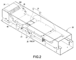
- Fig. 2 is a perspective view, taken from a lateral direction, showing the RF amplifier and the heat dissipation device after they are installed.
- the RF amplifier 10 is disposed at one side surface of the support plate 40, and the RF amplifier 10 is fixed inside the housing 30 via the support plate 40.
- the heat dissipation fan 24 is disposed at one side of the RF amplifier 10 and the fins 23. Furthermore, the forcible airflow generated by the heat dissipation fan 24 flows toward the RF amplifier 10 from one side to dissipate heat.
- the forcible airflow of the heat dissipation fan 24 is partially directed to pass through the wind guiding holes 250 to flow to electronic components, thereby directly dissipating heat of the RF amplifier 10 and increasing the heat dissipation efficiency of the electronic components.
- Fig. 3 is a perspective view, from another lateral direction, showing the RF amplifier and the heat dissipation device after completion of assembly.
- a plurality of fins 23 are disposed in parallel and spaced from each other on the heat conduction board 21.
- a plurality of heat pipes 22 are inserted through the fins 23, and the heat pipes 22 and the fins 23 are assembled at the other side surface of the support plate 40.
- the forcible airflow generated by the heat dissipation fan 24 flows from one side to the fins to dissipate heat, thereby increasing the heat dissipation efficiency of the electronic components.
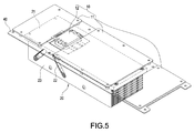
- Figs. 4 to 6 are a schematic view showing combining the RF amplifier and the heat dissipation device, a perspective view showing the RF amplifier and the heat dissipation device after they are combined, and a perspective view showing the heat dissipation device.
- Fig. 4 in the present embodiment, when the RF amplifier 10 is disposed at the support plate 40, the RF power element 12 is exposed at the other side surface of the support plate 40.
- the fins 23 having the heat pipes 22 inserted therein are assembled onto the heat conduction board 21 first, then one side surface of the heat conduction board 21 is arranged in direct contact with the RF power element 12, and the heat conduction board 21 is fastened to the support plate 40 by fastening elements.
- the RF amplifier 10 includes a plurality of circuit boards 11, and the circuit boards 11 are fixed in a spaced relationship on the support plate 40. Furthermore, the RF power element 12 is exposed from the support plate 40 and electrically connected to the circuit boards 11, and accordingly RF amplifier 10 and the heat dissipation device 20 are combined onto the support plate 40.
- the heat dissipation device 20 further includes a heat conduction block 26 (e.g. a copper block) disposed at the heat conduction board 21.
- a heat conduction block 26 e.g. a copper block
- One side of the heat conduction block 26 is in contact with the RF power element 12, and the other side of the heat conduction block 26 is embedded on the heat conduction board 21 to be thermally conductively coupled to the heat conduction board 21.
- Each of the heat pipes 22 includes an evaporation section 221 and a condensation section 222, and the evaporation section 221 of each of the heat pipes 22 is thermally conductively coupled to the heat conduction board 21. Moreover, one end (the evaporation section 221) of each of the heat pipes 22 is embedded in the heat conduction block 26, and the RF power element 12 is thermally conductively coupled to the heat conduction board 21 through the heat conduction block 26 and the evaporation sections 221 of the heat pipes 22.
- the fins 23 are disposed in parallel and spaced from each other on the heat conduction board 21, and the other end (the condensation section 222) of each of the heat pipes 22 is inserted through the fins 23, as more fully detailed hereinafter.
- the heat pipes 22 each are a U-shaped pipe.
- Each of the heat pipes 22 further includes a heat insulation section 223 connected to the evaporation section 221 and the condensation section 222.
- Each of the heat insulation sections 223 is in contact with the fins 23 at an outer side. It is preferable that the heat insulation sections 223 of the heat pipes 22 are disposed toward different directions, so that the condensation sections 222 are inserted in a spaced relationship through the fins 23. In other words, the heat pipes 22 are inserted through the fins 23 in different directions. Accordingly, the heat pipes 22 can conduct the heat uniformly to the fins 23, thus increasing the heat dissipation efficiency.
- Figs. 7 to 9 are cross-sectional views from two lateral directions and a partially enlarged view showing assembly of the RF amplifier with the heat dissipation device. As shown in Fig. 7 , it is clear that the RF power element 12 of the RF amplifier 10 is disposed between the heat conduction block 26 and the fins 23.
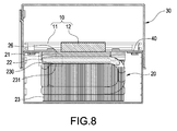
- each of the fins 23 includes a through hole 230 and a protruding ring 231 formed in the circumference of the through hole 230, and the protruding rings 231 of the fins 23 are in contact with an exterior surface of the heat pipes 22 to thereby obtaining a larger contact area with the heat pipes 22.
- each of the protruding rings 231 perpendicularly extends a distance H from the circumference of each of the through holes 230, and the fins 23 are spaced by the distance H to contact each other. Accordingly, the heat of the heat pipes 22 can be quickly conducted to the fins 23 via a larger contact area.
- the RF power element 12 When the RF amplifier 10 is in operation, the RF power element 12 generates a lot of heat and the temperature gets high. The heat of the RF power element 12 is conducted to the heat conduction block 26 and is conducted to the heat pipes 22 and the heat conduction board 21 via the heat conduction block 26. Then, the heat pipes 22 can quickly conduct the heat to the fins 23. Finally, the heat is distributed to the fins 23 uniformly to be dissipated away, and thereby quick heat dissipation is achieved, and the RF power element 12 can quickly reach a stable temperature.
Landscapes
- Engineering & Computer Science (AREA)
- Microelectronics & Electronic Packaging (AREA)
- Physics & Mathematics (AREA)
- Thermal Sciences (AREA)
- Power Engineering (AREA)
- Cooling Or The Like Of Electrical Apparatus (AREA)
- Amplifiers (AREA)
- Cooling Or The Like Of Semiconductors Or Solid State Devices (AREA)
Abstract
Description
- The present invention relates to a radio frequency (RF) amplifier system and, in particular, to an RF amplifier system which dissipates the heat of an RF amplifier system by means of heat pipes and fins.
- A radio frequency (RF) amplifier is an important part in an RF transmitter circuit. Its main function is to amplify the signal power and transmit the amplified signal to an antenna, so that the antenna can radiate the signal to a remote RF receiver. Since an RF power element in the RF amplifier is the most power-consuming part in the RF transmitter circuit and directly decides the quality of the transmitted signal, so design goals of the RF power element include output power, distortion, efficiency, bandwidth, and reliability.
- A conventional RF amplifier is limited to the low-voltage and high-current construction as which is the general manufacturing process for an RF power element. Therefore, the high-wattage RF power element normally utilizes a traditional parallel distributed structure to reduce current and distribute heat sources. In addition, the RF amplifier system is affected by other parasitic elements, so it normally adopts a large-size heat dissipation plate, which making the entire RF amplifier become too heavy. Moreover, the current RF power element also has a disadvantage of slow thermal equilibrium, and as a result, users need to wait a longer time for the system to warm up.
- The use of the conventional RF power element in the conventional RF amplifier system has disadvantages such as low conversion efficiency and too many components. In solution, industries have developed a new high-voltage RF power switch element to constitute the RF power amplifier. However, the new RF power switch element has high power dissipation per unit volume, and the heat source is concentrated, so heat dissipation is required to achieve stable temperatures and avoid damages due to high temperatures.
- Accordingly, the inventor made various studies to overcome the above-mentioned problems, on the basis of which the present invention is accomplished.
- One object of the present invention is to provide a radio frequency (RF) amplifier system and a heat dissipation device thereof, wherein an RF power element has high conversion efficiency, and the heat of the RF power element can be dissipated away quickly through the heat dissipation device, thereby achieving thermal equilibrium quickly.
- Another object of the present invention is to provide an RF amplifier system and a heat dissipation device, with simple heat dissipation structure and a reduced number of heat dissipation components, so that the heat dissipation device has reduced volume and weight.
- Accordingly, the present invention provides an RF amplifier system, comprising an RF amplifier and a heat dissipation device. The RF amplifier includes an RF power element. The heat dissipation device includes a heat conduction block, a heat conduction board, a plurality of heat pipes, and a plurality of fins. One side of the heat conduction block is in contact with the RF power element. The heat conduction board is thermally conductively coupled to the other side of the heat conduction block. An end of each of the heat pipes is disposed at the heat conduction block. The fins are disposed in parallel and spaced from each other on the heat conduction board, and the other end of each of the heat pipes are inserted through the fins. The heat generated from the RF power element is conducted to the heat conduction block and then is conducted to the fins through the heat conduction board and the heat pipes.
- Accordingly, the present invention provides a heat dissipation device of an RF amplifier system, for dissipating heat of an RF power element of the RF amplifier system. The heat dissipation device includes a heat conduction board, a plurality of heat pipes, and a plurality of fins. The heat conduction board is thermally conductively coupled to the RF power element. Each of the heat pipes includes an evaporation section and a condensation section, the evaporation section of each of the heat pipes is thermally conductively coupled to the heat conduction board, and the fins are arranged in parallel and spaced from each other. The condensation sections of the heat pipes are inserted through the fins. The heat generated by the RF power element is conducted to the heat conduction board and the evaporation sections of the heat pipes, and then is conducted to the fins through the condensation sections of the heat pipes.
- Compared to the heat dissipation structure of a conventional RF amplifier, the RF amplifier system of the present invention quickly transfers the heat of the RF power element by using a heat conductive component (e.g. a heat pipe) capable of phase changing. In addition, the phase-changing heat conductive component is inserted through the fins, so the heat can be quickly distributed to the fins, thereby optimizing heat dissipation performance, having a simple heat dissipation structure for the RF amplifier, and having a reduced number of the heat dissipation components, so that the whole heat dissipation device has reduced volume and weight. Furthermore, in this structure, the high-voltage RF power element can quickly reach thermal equilibrium and a stable temperature, and thereby the system can have a shortened warm-up waiting period for users. Moreover, the RF power element has high conversion efficiency, and the heat dissipation device has advantages such as reduced weight and volume, thus enhancing utility of the present invention.
- The disclosure will become more fully understood from the detailed description, and the drawings given herein below is for illustration only, and thus does not limit the disclosure, wherein:
-
FIG. 1 is a perspective exploded view showing an RF amplifier system according to the present invention; -
FIG. 2 is a perspective view, from a lateral direction, showing the RF amplifier system of the present invention; -
FIG. 3 is a perspective view, from another lateral direction, showing the RF amplifier system of the present invention; -
FIG. 4 is a schematic view showing combining an RF amplifier with a heat dissipation device; -
FIG. 5 is a perspective view showing the RF amplifier and the heat dissipation device after they are combined; -
FIG. 6 is a perspective view showing the heat dissipation device according to the present invention; -
FIG. 7 is a cross-sectional view from a lateral direction, showing assembly of the RF amplifier with the heat dissipation device; -
FIG. 8 is a cross-sectional view from another lateral direction, showing assembly of the RF amplifier with the heat dissipation device; and -
FIG. 9 is a partially enlarged view ofFIG. 8 . - Detailed descriptions and technical contents of the present invention are illustrated below in conjunction with the accompany drawings. However, it is to be understood that the descriptions and the accompany drawings disclosed herein are merely illustrative and exemplary and not intended to limit the scope of the present invention.
- Please refer to
Figs. 1 to 3 which are a perspective exploded view and perspective views from two lateral directions showing an RF amplifier system and a heat dissipation device thereof. The present invention provides an RF amplifier system and a heat dissipation device thereof. The RF amplifier system comprises anRF amplifier 10 and aheat dissipation device 20. Theheat dissipation device 20 is thermally conductively coupled to theRF amplifier 10 and dissipates the heat of theRF amplifier 10, thereby preventing overly high operation temperatures of theRF amplifier 10, thus maintaining normal operation of theRF amplifier 10 and a long lifespan thereof. - As shown in
Fig. 1 , according to one embodiment of the present invention, theRF amplifier 10 includes acircuit board 11, anRF power element 12 electrically connected to thecircuit board 11, and a resonant circuit (not illustrated) disposed at thecircuit board 11. In the present embodiment, theRF amplifier 10 includes a plurality ofcircuit boards 11; theRF power element 12 is disposed between twocircuit boards 11 and is electrically connected thereto. It is preferable that theRF power element 12 is a high-voltage RF power switch having high conversion efficiency. - The
heat dissipation device 20 includes a heat conduction board 21 (e.g. an aluminum board), a plurality ofheat pipes 22 and a plurality offins 23. Theheat conduction board 21 is thermally conductively coupled to theRF power element 12. Thefins 23 are disposed in parallel and spaced from each other on theheat conduction board 21. Theheat pipes 22 are inserted between theheat conduction board 21 and thefins 23. - It is preferable that the
heat dissipation device 20 further includes aheat dissipation fan 24 and awind guiding plate 25. Theheat dissipation fan 24 is disposed at one side of theRF amplifier 10 and thefins 23. Thewind guiding plate 25 includes a plurality of wind guidingholes 250. Furthermore, a forcible airflow generated by theheat dissipation fan 24 partially flows to thefins 23 to take away the heat of thefins 23, thereby indirectly dissipating the heat of theRF amplifier 10. Moreover, thewind guiding plate 25 guides a portion of the forcible airflow to pass through thewind guiding holes 250 to flow to theRF amplifier 10, thereby directly dissipating the heat of theRF amplifier 10. - It is preferable that, the present invention further includes a
housing 30 and asupport plate 40. When assembling, theRF amplifier 10 can be disposed at one side surface of thesupport plate 40. On the other hand, theheat pipes 22 and thefins 23 of theheat dissipation device 20 are assembled at the other side surface of thesupport plate 40. Then, thesupport plate 40 is fastened inside thehousing 30 by screws, and finally, theRF amplifier 10, theheat conduction plate 21, theheat pipes 22, and thefins 23 are assembled in the housing to complete assembly. - Please refer to
Fig. 2 which is a perspective view, taken from a lateral direction, showing the RF amplifier and the heat dissipation device after they are installed. As shown in the drawing, theRF amplifier 10 is disposed at one side surface of thesupport plate 40, and theRF amplifier 10 is fixed inside thehousing 30 via thesupport plate 40. Theheat dissipation fan 24 is disposed at one side of theRF amplifier 10 and thefins 23. Furthermore, the forcible airflow generated by theheat dissipation fan 24 flows toward theRF amplifier 10 from one side to dissipate heat. To be specific, by means of thewind guiding plate 25, the forcible airflow of theheat dissipation fan 24 is partially directed to pass through thewind guiding holes 250 to flow to electronic components, thereby directly dissipating heat of theRF amplifier 10 and increasing the heat dissipation efficiency of the electronic components. - Please refer to
Fig. 3 which is a perspective view, from another lateral direction, showing the RF amplifier and the heat dissipation device after completion of assembly. As shown in the drawing, a plurality offins 23 are disposed in parallel and spaced from each other on theheat conduction board 21. Furthermore, a plurality ofheat pipes 22 are inserted through thefins 23, and theheat pipes 22 and thefins 23 are assembled at the other side surface of thesupport plate 40. Moreover, the forcible airflow generated by theheat dissipation fan 24 flows from one side to the fins to dissipate heat, thereby increasing the heat dissipation efficiency of the electronic components. - Please refer to
Figs. 4 to 6 which are a schematic view showing combining the RF amplifier and the heat dissipation device, a perspective view showing the RF amplifier and the heat dissipation device after they are combined, and a perspective view showing the heat dissipation device. As shown inFig. 4 , in the present embodiment, when theRF amplifier 10 is disposed at thesupport plate 40, theRF power element 12 is exposed at the other side surface of thesupport plate 40. In addition, when assembling theheat dissipation device 20, thefins 23 having theheat pipes 22 inserted therein are assembled onto theheat conduction board 21 first, then one side surface of theheat conduction board 21 is arranged in direct contact with theRF power element 12, and theheat conduction board 21 is fastened to thesupport plate 40 by fastening elements. - As shown in
Fig. 5 , theRF amplifier 10 includes a plurality ofcircuit boards 11, and thecircuit boards 11 are fixed in a spaced relationship on thesupport plate 40. Furthermore, theRF power element 12 is exposed from thesupport plate 40 and electrically connected to thecircuit boards 11, and accordinglyRF amplifier 10 and theheat dissipation device 20 are combined onto thesupport plate 40. - As shown in
Fig. 6 , in the present embodiment, theheat dissipation device 20 further includes a heat conduction block 26 (e.g. a copper block) disposed at theheat conduction board 21. One side of theheat conduction block 26 is in contact with theRF power element 12, and the other side of theheat conduction block 26 is embedded on theheat conduction board 21 to be thermally conductively coupled to theheat conduction board 21. - Each of the
heat pipes 22 includes anevaporation section 221 and acondensation section 222, and theevaporation section 221 of each of theheat pipes 22 is thermally conductively coupled to theheat conduction board 21. Moreover, one end (the evaporation section 221) of each of theheat pipes 22 is embedded in theheat conduction block 26, and theRF power element 12 is thermally conductively coupled to theheat conduction board 21 through theheat conduction block 26 and theevaporation sections 221 of theheat pipes 22. Thefins 23 are disposed in parallel and spaced from each other on theheat conduction board 21, and the other end (the condensation section 222) of each of theheat pipes 22 is inserted through thefins 23, as more fully detailed hereinafter. - In one embodiment of the present invention, the
heat pipes 22 each are a U-shaped pipe. Each of theheat pipes 22 further includes aheat insulation section 223 connected to theevaporation section 221 and thecondensation section 222. Each of theheat insulation sections 223 is in contact with thefins 23 at an outer side. It is preferable that theheat insulation sections 223 of theheat pipes 22 are disposed toward different directions, so that thecondensation sections 222 are inserted in a spaced relationship through thefins 23. In other words, theheat pipes 22 are inserted through thefins 23 in different directions. Accordingly, theheat pipes 22 can conduct the heat uniformly to thefins 23, thus increasing the heat dissipation efficiency. - Please refer to
Figs. 7 to 9 which are cross-sectional views from two lateral directions and a partially enlarged view showing assembly of the RF amplifier with the heat dissipation device. As shown inFig. 7 , it is clear that theRF power element 12 of theRF amplifier 10 is disposed between theheat conduction block 26 and thefins 23. - Referring to
Fig. 8 , in the present embodiment, each of thefins 23 includes a throughhole 230 and aprotruding ring 231 formed in the circumference of the throughhole 230, and the protruding rings 231 of thefins 23 are in contact with an exterior surface of theheat pipes 22 to thereby obtaining a larger contact area with theheat pipes 22. - Referring to
Fig. 9 , in the present embodiment, each of the protruding rings 231 perpendicularly extends a distance H from the circumference of each of the throughholes 230, and thefins 23 are spaced by the distance H to contact each other. Accordingly, the heat of theheat pipes 22 can be quickly conducted to thefins 23 via a larger contact area. - When the
RF amplifier 10 is in operation, theRF power element 12 generates a lot of heat and the temperature gets high. The heat of theRF power element 12 is conducted to theheat conduction block 26 and is conducted to theheat pipes 22 and theheat conduction board 21 via theheat conduction block 26. Then, theheat pipes 22 can quickly conduct the heat to thefins 23. Finally, the heat is distributed to thefins 23 uniformly to be dissipated away, and thereby quick heat dissipation is achieved, and theRF power element 12 can quickly reach a stable temperature.
Claims (15)
- A radio frequency (RF) amplifier system, comprising:an RF amplifier (10) including an RF power element (12); anda heat dissipation device (20) including:a heat conduction block (26), one side of the heat conduction block (26) being in contact with the RF power element (12);a heat conduction board (21) thermally conductively coupled to the other side of the heat conduction block (26);a plurality of heat pipes (22), an end of each of the heat pipes (22) being disposed at the heat conduction block (26); anda plurality of fins (23) disposed in parallel and spaced from each other on the heat conduction board (21), the other end of each of the heat pipes (22) being inserted through the fins (23), wherein heat generated from the RF power element (12) is conducted to the heat conduction block (26), and then the heat is conducted to the fins (23) through the heat conduction board (21) and the heat pipes (22).
- The RF amplifier system of claim 1, wherein each of the fins (23) includes a through hole (230) corresponding to each of the heat pipes (23) and a protruding ring (231) formed in the circumference of the through hole (230), and the protruding rings (231) are in contact with the heat pipes (23).
- The RF amplifier system of claim 2, wherein each of the protruding rings (231) perpendicularly extends a distance from the circumference of each of the through holes (230), and the fins (23) are spaced by the distance to contact with each other.
- The RF amplifier system of any of the claims 1 to 3, wherein the heat pipes (22) are inserted through the fins (23) in different directions.
- The RF amplifier system of any of the claims 1 to 4, wherein the heat dissipation device (20) further includes a heat dissipation fan (24) and a wind guiding plate (25), the heat dissipation fan (24) is disposed at one side of the RF amplifier (10) and the fins (23), the wind guiding plate (25) includes a plurality of wind guiding holes (250), and a forcible airflow generated by the heat dissipation fan (24) partially flows to the fins (23) and partially passes through the wind guiding holes (250) to flow to the RF amplifier (10).
- The RF amplifier system of any of the claims 1 to 5, further comprising a housing (30) and a support plate (40), the RF amplifier (10) further including a circuit board (11) disposed with the RF power element (12), the RF amplifier (10), the heat conduction board (21), the heat pipes (22) and the fins (23) being disposed in the housing (30), the circuit board (11) being disposed on the support plate (40), the support plate (40) being assembled inside the housing (30).
- A heat dissipation device of an RF amplifier system, for dissipating heat of an RF power element (12) of a RF amplifier (10), comprising:a heat conduction board (21) thermally conductively coupled to the RF power element (12);a plurality of heat pipes (22), each of the heat pipes (22) including an evaporation section (221) and a condensation section (222), the evaporation section (221) of each of the heat pipes (22) being thermally conductively coupled to the heat conduction board (21); anda plurality of fins (23) arranged in parallel and spaced from each other, the condensation section (222) of the heat pipes (22) being inserted through the fins (23), wherein heat generated by the RF power element (12) is conducted to the heat conduction board (21) and the evaporation section (221) of each of the heat pipes (22), and then is conducted to the fins (23) through the condensation section (222) of each of the heat pipes (22).
- The heat dissipation device of the RF amplifier system of claim 7, wherein the RF amplifier (10) further includes a circuit board (11), the circuit board (11) is electrically connected to the RF power element (12), and the RF amplifier (10) also includes a resonant circuit disposed at the circuit board (11).
- The heat dissipation device of the RF amplifier system of claim 7 or 8, wherein the heat dissipation device (20) further includes a heat conduction block (26) disposed at the heat conduction board (21), the heat conduction block (26) is in contact with the RF power element (12), the evaporation section (221) of each of the heat pipes (22) is embedded in the heat conduction block (26), and the RF power element (12) is thermally conductively coupled to the heat conduction board (21) through the heat conduction block (26) and the evaporation sections (221) of the heat pipes (22).
- The heat dissipation device of the RF amplifier system of any of the claims 7 to 9, wherein each of the fins (23) includes a through hole (230) corresponding to each of the heat pipes (22) and includes a protruding ring (231) formed in the circumference of the through hole (230), and the protruding rings (231) are in contact with the condensation section (222) of the heat pipes (22).
- The heat dissipation device of the RF amplifier system of claim 10, wherein each of the protruding rings (231) perpendicularly extends a distance from the circumference of the through hole (230), and the fins (23) are spaced by the distance to contact with each other.
- The heat dissipation device of the RF amplifier system of any of the claims 7 to 11, wherein the heat dissipation device (20) further includes a heat dissipation fan (24) and a wind guiding plate (25), the heat dissipation fan (24) is disposed at one side of the RF amplifier (10) and the fins (23), the wind guiding plate (25) includes a plurality of wind guiding holes (250), and a forcible airflow generated by the heat dissipation fan (24) partially flows to the fins (23) and partially passes through the wind guiding holes (250) to flow to the RF amplifier (10).
- The heat dissipation device of the RF amplifier system of any of the claims 7 to 12, further comprising a housing (30) and a support plate (40), the heat conduction board (21), the heat pipes (22) and the fins (23) being disposed in the housing (30), the RF amplifier (10) being disposed on the support plate (40), the support plate (40) being assembled inside the housing (30).
- The heat dissipation device of the RF amplifier system of any of claims 7 to 13, wherein each of the heat pipes (22) further includes a heat insulation section (223) connected to the evaporation section (221) and the condensation section (222), and each of the heat insulation sections (223) is in contact with the fins (23) at an outer side.
- The heat dissipation device of the RF amplifier system of claim 14, wherein the heat insulation sections (223) of the heat pipes (22) are disposed toward different directions, so that the condensation sections (222) of the heat pipes (22) are inserted in a spaced relationship through the fins (23).
Applications Claiming Priority (1)
| Application Number | Priority Date | Filing Date | Title |
|---|---|---|---|
| TW105105592A TWI618477B (en) | 2016-02-25 | 2016-02-25 | RF amplification system and its heat sink |
Publications (3)
| Publication Number | Publication Date |
|---|---|
| EP3255968A1 true EP3255968A1 (en) | 2017-12-13 |
| EP3255968B1 EP3255968B1 (en) | 2021-01-06 |
| EP3255968B8 EP3255968B8 (en) | 2021-03-24 |
Family
ID=56979388
Family Applications (1)
| Application Number | Title | Priority Date | Filing Date |
|---|---|---|---|
| EP16189381.3A Active EP3255968B8 (en) | 2016-02-25 | 2016-09-19 | Radio frequency amplifier system and heat dissipation device thereof |
Country Status (4)
| Country | Link |
|---|---|
| US (1) | US10110172B2 (en) |
| EP (1) | EP3255968B8 (en) |
| JP (1) | JP6448595B2 (en) |
| TW (1) | TWI618477B (en) |
Families Citing this family (7)
| Publication number | Priority date | Publication date | Assignee | Title |
|---|---|---|---|---|
| FR3059466B1 (en) * | 2016-11-30 | 2019-07-05 | Sagemcom Broadband Sas | HEAT EXHAUST DEVICE |
| KR101922991B1 (en) * | 2016-12-23 | 2018-11-28 | 효성중공업 주식회사 | Power device cooling device for power conversion device |
| JP7294762B2 (en) * | 2019-03-13 | 2023-06-20 | Fdk株式会社 | Electronics |
| JP7590571B2 (en) * | 2020-12-02 | 2024-11-26 | ケーエムダブリュ・インコーポレーテッド | Antenna Device |
| CN114630558B (en) * | 2022-01-30 | 2024-11-29 | 华为数字能源技术有限公司 | Heat dissipation system, power supply system and charging pile |
| CN114980709B (en) * | 2022-07-28 | 2022-09-30 | 深圳市德兰明海科技有限公司 | Double-air-duct heat dissipation assembly and inverter using same |
| CN116367510B (en) * | 2023-04-17 | 2025-12-05 | 苏州钧灏电力有限公司 | A converter heat dissipation device and its control method |
Citations (3)
| Publication number | Priority date | Publication date | Assignee | Title |
|---|---|---|---|---|
| EP2290681A2 (en) * | 2009-08-27 | 2011-03-02 | Hitachi, Ltd. | Power conversion device |
| US20130155616A1 (en) * | 2011-12-16 | 2013-06-20 | Delta Electronics (Shanghai) Co., Ltd. | Hybrid heat sink and hybrid heat sink assembly for power module |
| US20150016171A1 (en) * | 2013-07-10 | 2015-01-15 | Hitachi, Ltd. | Traction converter and railway vehicle |
Family Cites Families (15)
| Publication number | Priority date | Publication date | Assignee | Title |
|---|---|---|---|---|
| JPS52125280A (en) * | 1976-04-14 | 1977-10-20 | Hitachi Ltd | Cooling process for electronic device |
| JPS6034280B2 (en) * | 1977-05-25 | 1985-08-07 | 三菱電機株式会社 | Electronic parts storage board |
| JPH07211823A (en) * | 1994-01-24 | 1995-08-11 | Nippon Hoso Kyokai <Nhk> | Imaging device |
| JP3214664B2 (en) * | 1995-05-25 | 2001-10-02 | 松下電器産業株式会社 | High frequency device with superconducting element and temperature controller |
| JP3665508B2 (en) * | 1999-05-18 | 2005-06-29 | 古河電気工業株式会社 | Heat sink with fins |
| US7198096B2 (en) * | 2002-11-26 | 2007-04-03 | Thermotek, Inc. | Stacked low profile cooling system and method for making same |
| US7857037B2 (en) * | 2001-11-27 | 2010-12-28 | Thermotek, Inc. | Geometrically reoriented low-profile phase plane heat pipes |
| US7342788B2 (en) * | 2004-03-12 | 2008-03-11 | Powerwave Technologies, Inc. | RF power amplifier assembly with heat pipe enhanced pallet |
| US7812604B2 (en) * | 2007-11-14 | 2010-10-12 | General Electric Company | Thermal management system for cooling a heat generating component of a magnetic resonance imaging apparatus |
| CN101568247B (en) * | 2008-04-25 | 2012-09-05 | 深圳迈瑞生物医疗电子股份有限公司 | Shielding insulating radiating system |
| JP2011094888A (en) * | 2009-10-30 | 2011-05-12 | Fujitsu Ltd | Heat radiator and method of manufacturing the heat radiator |
| CN101808494B (en) * | 2010-03-26 | 2012-03-21 | 海能达通信股份有限公司 | Radio frequency high-power heat pipe radiator |
| JP2013531389A (en) * | 2010-07-16 | 2013-08-01 | エンブレーション リミテッド | Apparatus and method for taking a thermal interface |
| JP5594784B2 (en) * | 2011-06-29 | 2014-09-24 | エヌイーシーコンピュータテクノ株式会社 | Heat sink cooler |
| TWM462501U (en) * | 2013-04-24 | 2013-09-21 | Micro Star Int Co Ltd | Heat dissipation system |
-
2016
- 2016-02-25 TW TW105105592A patent/TWI618477B/en active
- 2016-09-19 EP EP16189381.3A patent/EP3255968B8/en active Active
- 2016-09-21 JP JP2016184619A patent/JP6448595B2/en active Active
- 2016-09-21 US US15/271,404 patent/US10110172B2/en active Active
Patent Citations (3)
| Publication number | Priority date | Publication date | Assignee | Title |
|---|---|---|---|---|
| EP2290681A2 (en) * | 2009-08-27 | 2011-03-02 | Hitachi, Ltd. | Power conversion device |
| US20130155616A1 (en) * | 2011-12-16 | 2013-06-20 | Delta Electronics (Shanghai) Co., Ltd. | Hybrid heat sink and hybrid heat sink assembly for power module |
| US20150016171A1 (en) * | 2013-07-10 | 2015-01-15 | Hitachi, Ltd. | Traction converter and railway vehicle |
Also Published As
| Publication number | Publication date |
|---|---|
| EP3255968B8 (en) | 2021-03-24 |
| TW201731370A (en) | 2017-09-01 |
| TWI618477B (en) | 2018-03-11 |
| US10110172B2 (en) | 2018-10-23 |
| US20170250659A1 (en) | 2017-08-31 |
| JP6448595B2 (en) | 2019-01-09 |
| JP2017152671A (en) | 2017-08-31 |
| EP3255968B1 (en) | 2021-01-06 |
Similar Documents
| Publication | Publication Date | Title |
|---|---|---|
| US10110172B2 (en) | Radio frequency amplifier system and heat dissipation device thereof | |
| EP2228595B1 (en) | LED lamp assembly | |
| WO2020073897A1 (en) | Heat Dissipation Assembly and Communication Module | |
| US20150201530A1 (en) | Heat Spreading Packaging Apparatus | |
| KR101502269B1 (en) | Speaker device | |
| CN110494018B (en) | an optical module | |
| US20190104644A1 (en) | Electronic device | |
| CN208937890U (en) | Radiator and projector | |
| US20160212881A1 (en) | Heat dissipation device and method of dissipating heat | |
| US9326424B2 (en) | Heat sink assembly and method of utilizing a heat sink assembly | |
| JP2009223881A (en) | Radio communication apparatus | |
| CN205408372U (en) | Semiconductor power source module and have its microwave applicator spare | |
| CN107124850B (en) | Radio frequency amplification system and heat dissipation device thereof | |
| CN216626450U (en) | A 5G signal communication high frequency circuit board | |
| JP6907672B2 (en) | Heat dissipation device | |
| JP3209591U (en) | Heat dissipation device assembly structure | |
| US20140352925A1 (en) | Heat pipe structure | |
| CN102316701A (en) | Heat radiation device | |
| JP2011210806A (en) | Electronic apparatus | |
| US20180288901A1 (en) | Heat dissipation device having compact vapor chamber | |
| KR101207934B1 (en) | Structure of heat sink | |
| CN210246720U (en) | Universal micropower short-distance wireless transmitting equipment | |
| CN219812395U (en) | Heat dissipation mechanism and energy storage equipment | |
| CN219999879U (en) | A TR module and a TR combination module | |
| CN219834548U (en) | Compact detector shell heat radiation structure |
Legal Events
| Date | Code | Title | Description |
|---|---|---|---|
| PUAI | Public reference made under article 153(3) epc to a published international application that has entered the european phase |
Free format text: ORIGINAL CODE: 0009012 |
|
| STAA | Information on the status of an ep patent application or granted ep patent |
Free format text: STATUS: THE APPLICATION HAS BEEN PUBLISHED |
|
| AK | Designated contracting states |
Kind code of ref document: A1 Designated state(s): AL AT BE BG CH CY CZ DE DK EE ES FI FR GB GR HR HU IE IS IT LI LT LU LV MC MK MT NL NO PL PT RO RS SE SI SK SM TR |
|
| AX | Request for extension of the european patent |
Extension state: BA ME |
|
| STAA | Information on the status of an ep patent application or granted ep patent |
Free format text: STATUS: REQUEST FOR EXAMINATION WAS MADE |
|
| 17P | Request for examination filed |
Effective date: 20180518 |
|
| RBV | Designated contracting states (corrected) |
Designated state(s): AL AT BE BG CH CY CZ DE DK EE ES FI FR GB GR HR HU IE IS IT LI LT LU LV MC MK MT NL NO PL PT RO RS SE SI SK SM TR |
|
| GRAP | Despatch of communication of intention to grant a patent |
Free format text: ORIGINAL CODE: EPIDOSNIGR1 |
|
| STAA | Information on the status of an ep patent application or granted ep patent |
Free format text: STATUS: GRANT OF PATENT IS INTENDED |
|
| RIC1 | Information provided on ipc code assigned before grant |
Ipc: H05K 7/20 20060101AFI20200629BHEP Ipc: H03F 1/30 20060101ALI20200629BHEP Ipc: H01L 23/427 20060101ALI20200629BHEP Ipc: H01L 23/467 20060101ALI20200629BHEP Ipc: H01L 23/367 20060101ALI20200629BHEP |
|
| INTG | Intention to grant announced |
Effective date: 20200731 |
|
| GRAS | Grant fee paid |
Free format text: ORIGINAL CODE: EPIDOSNIGR3 |
|
| GRAA | (expected) grant |
Free format text: ORIGINAL CODE: 0009210 |
|
| STAA | Information on the status of an ep patent application or granted ep patent |
Free format text: STATUS: THE PATENT HAS BEEN GRANTED |
|
| AK | Designated contracting states |
Kind code of ref document: B1 Designated state(s): AL AT BE BG CH CY CZ DE DK EE ES FI FR GB GR HR HU IE IS IT LI LT LU LV MC MK MT NL NO PL PT RO RS SE SI SK SM TR |
|
| REG | Reference to a national code |
Ref country code: GB Ref legal event code: FG4D |
|
| REG | Reference to a national code |
Ref country code: AT Ref legal event code: REF Ref document number: 1353789 Country of ref document: AT Kind code of ref document: T Effective date: 20210115 Ref country code: CH Ref legal event code: EP |
|
| REG | Reference to a national code |
Ref country code: DE Ref legal event code: R096 Ref document number: 602016050908 Country of ref document: DE |
|
| GRAT | Correction requested after decision to grant or after decision to maintain patent in amended form |
Free format text: ORIGINAL CODE: EPIDOSNCDEC |
|
| REG | Reference to a national code |
Ref country code: IE Ref legal event code: FG4D |
|
| REG | Reference to a national code |
Ref country code: NL Ref legal event code: FP |
|
| REG | Reference to a national code |
Ref country code: CH Ref legal event code: PK Free format text: BERICHTIGUNG B8 |
|
| RAP2 | Party data changed (patent owner data changed or rights of a patent transferred) |
Owner name: DELTA ELECTRONICS, INC. |
|
| REG | Reference to a national code |
Ref country code: AT Ref legal event code: MK05 Ref document number: 1353789 Country of ref document: AT Kind code of ref document: T Effective date: 20210106 |
|
| REG | Reference to a national code |
Ref country code: LT Ref legal event code: MG9D |
|
| PG25 | Lapsed in a contracting state [announced via postgrant information from national office to epo] |
Ref country code: HR Free format text: LAPSE BECAUSE OF FAILURE TO SUBMIT A TRANSLATION OF THE DESCRIPTION OR TO PAY THE FEE WITHIN THE PRESCRIBED TIME-LIMIT Effective date: 20210106 Ref country code: FI Free format text: LAPSE BECAUSE OF FAILURE TO SUBMIT A TRANSLATION OF THE DESCRIPTION OR TO PAY THE FEE WITHIN THE PRESCRIBED TIME-LIMIT Effective date: 20210106 Ref country code: GR Free format text: LAPSE BECAUSE OF FAILURE TO SUBMIT A TRANSLATION OF THE DESCRIPTION OR TO PAY THE FEE WITHIN THE PRESCRIBED TIME-LIMIT Effective date: 20210407 Ref country code: LT Free format text: LAPSE BECAUSE OF FAILURE TO SUBMIT A TRANSLATION OF THE DESCRIPTION OR TO PAY THE FEE WITHIN THE PRESCRIBED TIME-LIMIT Effective date: 20210106 Ref country code: BG Free format text: LAPSE BECAUSE OF FAILURE TO SUBMIT A TRANSLATION OF THE DESCRIPTION OR TO PAY THE FEE WITHIN THE PRESCRIBED TIME-LIMIT Effective date: 20210406 Ref country code: PT Free format text: LAPSE BECAUSE OF FAILURE TO SUBMIT A TRANSLATION OF THE DESCRIPTION OR TO PAY THE FEE WITHIN THE PRESCRIBED TIME-LIMIT Effective date: 20210506 Ref country code: NO Free format text: LAPSE BECAUSE OF FAILURE TO SUBMIT A TRANSLATION OF THE DESCRIPTION OR TO PAY THE FEE WITHIN THE PRESCRIBED TIME-LIMIT Effective date: 20210406 |
|
| PG25 | Lapsed in a contracting state [announced via postgrant information from national office to epo] |
Ref country code: SE Free format text: LAPSE BECAUSE OF FAILURE TO SUBMIT A TRANSLATION OF THE DESCRIPTION OR TO PAY THE FEE WITHIN THE PRESCRIBED TIME-LIMIT Effective date: 20210106 Ref country code: AT Free format text: LAPSE BECAUSE OF FAILURE TO SUBMIT A TRANSLATION OF THE DESCRIPTION OR TO PAY THE FEE WITHIN THE PRESCRIBED TIME-LIMIT Effective date: 20210106 Ref country code: PL Free format text: LAPSE BECAUSE OF FAILURE TO SUBMIT A TRANSLATION OF THE DESCRIPTION OR TO PAY THE FEE WITHIN THE PRESCRIBED TIME-LIMIT Effective date: 20210106 Ref country code: LV Free format text: LAPSE BECAUSE OF FAILURE TO SUBMIT A TRANSLATION OF THE DESCRIPTION OR TO PAY THE FEE WITHIN THE PRESCRIBED TIME-LIMIT Effective date: 20210106 Ref country code: RS Free format text: LAPSE BECAUSE OF FAILURE TO SUBMIT A TRANSLATION OF THE DESCRIPTION OR TO PAY THE FEE WITHIN THE PRESCRIBED TIME-LIMIT Effective date: 20210106 |
|
| PG25 | Lapsed in a contracting state [announced via postgrant information from national office to epo] |
Ref country code: IS Free format text: LAPSE BECAUSE OF FAILURE TO SUBMIT A TRANSLATION OF THE DESCRIPTION OR TO PAY THE FEE WITHIN THE PRESCRIBED TIME-LIMIT Effective date: 20210506 |
|
| REG | Reference to a national code |
Ref country code: DE Ref legal event code: R097 Ref document number: 602016050908 Country of ref document: DE |
|
| PG25 | Lapsed in a contracting state [announced via postgrant information from national office to epo] |
Ref country code: CZ Free format text: LAPSE BECAUSE OF FAILURE TO SUBMIT A TRANSLATION OF THE DESCRIPTION OR TO PAY THE FEE WITHIN THE PRESCRIBED TIME-LIMIT Effective date: 20210106 Ref country code: EE Free format text: LAPSE BECAUSE OF FAILURE TO SUBMIT A TRANSLATION OF THE DESCRIPTION OR TO PAY THE FEE WITHIN THE PRESCRIBED TIME-LIMIT Effective date: 20210106 Ref country code: SM Free format text: LAPSE BECAUSE OF FAILURE TO SUBMIT A TRANSLATION OF THE DESCRIPTION OR TO PAY THE FEE WITHIN THE PRESCRIBED TIME-LIMIT Effective date: 20210106 |
|
| PLBE | No opposition filed within time limit |
Free format text: ORIGINAL CODE: 0009261 |
|
| STAA | Information on the status of an ep patent application or granted ep patent |
Free format text: STATUS: NO OPPOSITION FILED WITHIN TIME LIMIT |
|
| PG25 | Lapsed in a contracting state [announced via postgrant information from national office to epo] |
Ref country code: DK Free format text: LAPSE BECAUSE OF FAILURE TO SUBMIT A TRANSLATION OF THE DESCRIPTION OR TO PAY THE FEE WITHIN THE PRESCRIBED TIME-LIMIT Effective date: 20210106 Ref country code: SK Free format text: LAPSE BECAUSE OF FAILURE TO SUBMIT A TRANSLATION OF THE DESCRIPTION OR TO PAY THE FEE WITHIN THE PRESCRIBED TIME-LIMIT Effective date: 20210106 Ref country code: RO Free format text: LAPSE BECAUSE OF FAILURE TO SUBMIT A TRANSLATION OF THE DESCRIPTION OR TO PAY THE FEE WITHIN THE PRESCRIBED TIME-LIMIT Effective date: 20210106 |
|
| 26N | No opposition filed |
Effective date: 20211007 |
|
| PG25 | Lapsed in a contracting state [announced via postgrant information from national office to epo] |
Ref country code: ES Free format text: LAPSE BECAUSE OF FAILURE TO SUBMIT A TRANSLATION OF THE DESCRIPTION OR TO PAY THE FEE WITHIN THE PRESCRIBED TIME-LIMIT Effective date: 20210106 Ref country code: AL Free format text: LAPSE BECAUSE OF FAILURE TO SUBMIT A TRANSLATION OF THE DESCRIPTION OR TO PAY THE FEE WITHIN THE PRESCRIBED TIME-LIMIT Effective date: 20210106 |
|
| PG25 | Lapsed in a contracting state [announced via postgrant information from national office to epo] |
Ref country code: SI Free format text: LAPSE BECAUSE OF FAILURE TO SUBMIT A TRANSLATION OF THE DESCRIPTION OR TO PAY THE FEE WITHIN THE PRESCRIBED TIME-LIMIT Effective date: 20210106 |
|
| PG25 | Lapsed in a contracting state [announced via postgrant information from national office to epo] |
Ref country code: IT Free format text: LAPSE BECAUSE OF FAILURE TO SUBMIT A TRANSLATION OF THE DESCRIPTION OR TO PAY THE FEE WITHIN THE PRESCRIBED TIME-LIMIT Effective date: 20210106 |
|
| REG | Reference to a national code |
Ref country code: CH Ref legal event code: PL |
|
| REG | Reference to a national code |
Ref country code: BE Ref legal event code: MM Effective date: 20210930 |
|
| PG25 | Lapsed in a contracting state [announced via postgrant information from national office to epo] |
Ref country code: IS Free format text: LAPSE BECAUSE OF FAILURE TO SUBMIT A TRANSLATION OF THE DESCRIPTION OR TO PAY THE FEE WITHIN THE PRESCRIBED TIME-LIMIT Effective date: 20210506 Ref country code: MC Free format text: LAPSE BECAUSE OF FAILURE TO SUBMIT A TRANSLATION OF THE DESCRIPTION OR TO PAY THE FEE WITHIN THE PRESCRIBED TIME-LIMIT Effective date: 20210106 |
|
| PG25 | Lapsed in a contracting state [announced via postgrant information from national office to epo] |
Ref country code: LU Free format text: LAPSE BECAUSE OF NON-PAYMENT OF DUE FEES Effective date: 20210919 Ref country code: IE Free format text: LAPSE BECAUSE OF NON-PAYMENT OF DUE FEES Effective date: 20210919 Ref country code: BE Free format text: LAPSE BECAUSE OF NON-PAYMENT OF DUE FEES Effective date: 20210930 |
|
| PG25 | Lapsed in a contracting state [announced via postgrant information from national office to epo] |
Ref country code: LI Free format text: LAPSE BECAUSE OF NON-PAYMENT OF DUE FEES Effective date: 20210930 Ref country code: CH Free format text: LAPSE BECAUSE OF NON-PAYMENT OF DUE FEES Effective date: 20210930 |
|
| PG25 | Lapsed in a contracting state [announced via postgrant information from national office to epo] |
Ref country code: HU Free format text: LAPSE BECAUSE OF FAILURE TO SUBMIT A TRANSLATION OF THE DESCRIPTION OR TO PAY THE FEE WITHIN THE PRESCRIBED TIME-LIMIT; INVALID AB INITIO Effective date: 20160919 |
|
| PG25 | Lapsed in a contracting state [announced via postgrant information from national office to epo] |
Ref country code: CY Free format text: LAPSE BECAUSE OF FAILURE TO SUBMIT A TRANSLATION OF THE DESCRIPTION OR TO PAY THE FEE WITHIN THE PRESCRIBED TIME-LIMIT Effective date: 20210106 |
|
| PG25 | Lapsed in a contracting state [announced via postgrant information from national office to epo] |
Ref country code: MK Free format text: LAPSE BECAUSE OF FAILURE TO SUBMIT A TRANSLATION OF THE DESCRIPTION OR TO PAY THE FEE WITHIN THE PRESCRIBED TIME-LIMIT Effective date: 20210106 |
|
| PG25 | Lapsed in a contracting state [announced via postgrant information from national office to epo] |
Ref country code: MT Free format text: LAPSE BECAUSE OF FAILURE TO SUBMIT A TRANSLATION OF THE DESCRIPTION OR TO PAY THE FEE WITHIN THE PRESCRIBED TIME-LIMIT Effective date: 20210106 |
|
| PGFP | Annual fee paid to national office [announced via postgrant information from national office to epo] |
Ref country code: NL Payment date: 20250814 Year of fee payment: 10 |
|
| PGFP | Annual fee paid to national office [announced via postgrant information from national office to epo] |
Ref country code: DE Payment date: 20250722 Year of fee payment: 10 |
|
| PGFP | Annual fee paid to national office [announced via postgrant information from national office to epo] |
Ref country code: GB Payment date: 20250731 Year of fee payment: 10 |
|
| PGFP | Annual fee paid to national office [announced via postgrant information from national office to epo] |
Ref country code: FR Payment date: 20250708 Year of fee payment: 10 |
|
| PG25 | Lapsed in a contracting state [announced via postgrant information from national office to epo] |
Ref country code: TR Free format text: LAPSE BECAUSE OF FAILURE TO SUBMIT A TRANSLATION OF THE DESCRIPTION OR TO PAY THE FEE WITHIN THE PRESCRIBED TIME-LIMIT Effective date: 20210106 |