EP3255790A1 - Linear isolation amplifier with output dc voltage cancellation - Google Patents
Linear isolation amplifier with output dc voltage cancellation Download PDFInfo
- Publication number
- EP3255790A1 EP3255790A1 EP17161108.0A EP17161108A EP3255790A1 EP 3255790 A1 EP3255790 A1 EP 3255790A1 EP 17161108 A EP17161108 A EP 17161108A EP 3255790 A1 EP3255790 A1 EP 3255790A1
- Authority
- EP
- European Patent Office
- Prior art keywords
- signal
- output terminal
- output
- differential input
- amplifier
- Prior art date
- Legal status (The legal status is an assumption and is not a legal conclusion. Google has not performed a legal analysis and makes no representation as to the accuracy of the status listed.)
- Withdrawn
Links
Images


Classifications
-
- H—ELECTRICITY
- H03—ELECTRONIC CIRCUITRY
- H03F—AMPLIFIERS
- H03F3/00—Amplifiers with only discharge tubes or only semiconductor devices as amplifying elements
- H03F3/04—Amplifiers with only discharge tubes or only semiconductor devices as amplifying elements with semiconductor devices only
- H03F3/08—Amplifiers with only discharge tubes or only semiconductor devices as amplifying elements with semiconductor devices only controlled by light
- H03F3/085—Amplifiers with only discharge tubes or only semiconductor devices as amplifying elements with semiconductor devices only controlled by light using opto-couplers between stages
-
- H—ELECTRICITY
- H03—ELECTRONIC CIRCUITRY
- H03F—AMPLIFIERS
- H03F1/00—Details of amplifiers with only discharge tubes, only semiconductor devices or only unspecified devices as amplifying elements
- H03F1/30—Modifications of amplifiers to reduce influence of variations of temperature or supply voltage or other physical parameters
-
- H—ELECTRICITY
- H03—ELECTRONIC CIRCUITRY
- H03F—AMPLIFIERS
- H03F3/00—Amplifiers with only discharge tubes or only semiconductor devices as amplifying elements
- H03F3/45—Differential amplifiers
-
- H—ELECTRICITY
- H03—ELECTRONIC CIRCUITRY
- H03F—AMPLIFIERS
- H03F3/00—Amplifiers with only discharge tubes or only semiconductor devices as amplifying elements
- H03F3/68—Combinations of amplifiers, e.g. multi-channel amplifiers for stereophonics
-
- H—ELECTRICITY
- H04—ELECTRIC COMMUNICATION TECHNIQUE
- H04B—TRANSMISSION
- H04B10/00—Transmission systems employing electromagnetic waves other than radio-waves, e.g. infrared, visible or ultraviolet light, or employing corpuscular radiation, e.g. quantum communication
- H04B10/80—Optical aspects relating to the use of optical transmission for specific applications, not provided for in groups H04B10/03 - H04B10/70, e.g. optical power feeding or optical transmission through water
- H04B10/801—Optical aspects relating to the use of optical transmission for specific applications, not provided for in groups H04B10/03 - H04B10/70, e.g. optical power feeding or optical transmission through water using optical interconnects, e.g. light coupled isolators, circuit board interconnections
- H04B10/802—Optical aspects relating to the use of optical transmission for specific applications, not provided for in groups H04B10/03 - H04B10/70, e.g. optical power feeding or optical transmission through water using optical interconnects, e.g. light coupled isolators, circuit board interconnections for isolation, e.g. using optocouplers
-
- H—ELECTRICITY
- H03—ELECTRONIC CIRCUITRY
- H03F—AMPLIFIERS
- H03F2200/00—Indexing scheme relating to amplifiers
- H03F2200/171—A filter circuit coupled to the output of an amplifier
-
- H—ELECTRICITY
- H03—ELECTRONIC CIRCUITRY
- H03F—AMPLIFIERS
- H03F2200/00—Indexing scheme relating to amplifiers
- H03F2200/264—An operational amplifier based integrator or transistor based integrator being used in an amplifying circuit
-
- H—ELECTRICITY
- H03—ELECTRONIC CIRCUITRY
- H03F—AMPLIFIERS
- H03F2200/00—Indexing scheme relating to amplifiers
- H03F2200/375—Circuitry to compensate the offset being present in an amplifier
Definitions
- the present invention relates generally to electronic circuits, and particularly to linear isolation amplifiers.
- an electronic signal either a voltage or current signal
- An example of such a case is provided by a circuit of which one part is in contact with a human, such as when a patient is monitored by one part of the circuit, and the other part is connected to external electronic equipment.
- Providing complete ohmic isolation between the two parts of the circuit ensures that an electronic malfunction in the external electronic equipment will not cause a harmful current to flow through the patient.
- a widely used electronic circuit for passing signals, while isolating the two parts of the circuit is a linear isolation amplifier, based on a linear opto-coupler.
- signal is used in the present description and in the claims to denote an electronic voltage or current signal, unless otherwise specified.
- the linear opto-coupler transmits a signal through one or more pairs of an optical emitter and a receiver, so that the electronic signal is translated first into an optical signal and then back into an electronic signal. Due to the asymmetrical construction of the emitter-receiver pairs and the non-conducting (dielectric) gap transmitting the emitted photons, the signal will travel in one direction only, without any possibility of a reverse current flowing towards the patient. The use of a photonic circuit, however, imposes a condition of unipolarity on the transmitted signal.
- the signal to be transmitted is a pure AC-signal
- it is converted to a positive unipolar signal before being input to the linear opto-coupler.
- This conversion may be accomplished by a pre-amplifier within the linear isolation amplifier, which pre-amplifier adds a fixed, positive DC-reference voltage to the AC-signal, thus creating a positive unipolar signal with a sufficiently high positive minimum value.
- the positive unipolar signal has been passed through the linear opto-coupler, its AC-component can be recovered.
- Embodiments of the present invention that are described hereinbelow provide improved isolation circuits and a method for their use.
- an electronic circuit including an isolation amplifier, having a first input terminal coupled to receive an input AC-signal and including a linear opto-isolator, which has a first output terminal and is coupled to provide at the first output terminal a unipolar signal, having an AC-component proportional to the input signal, and a transimpedance receiver, including a first operational amplifier, having a second output terminal and first and second differential input terminals, with the first differential input terminal coupled to receive and amplify the unipolar output signal from the first output terminal so as to provide an output signal from the circuit at the second output terminal, and a second operational amplifier, which is configured as an integrator, and which has a third output terminal coupled to the second differential input terminal and has third and fourth differential input terminals, with the third differential input terminal coupled to receive the output signal from the second output terminal and the fourth differential input terminal connected to a ground.
- an isolation amplifier having a first input terminal coupled to receive an input AC-signal and including a linear opto-isolator, which has a first output terminal and is
- the transimpedance receiver includes an input resistor and a feedback capacitor coupled to the second operational amplifier, with values chosen so that the transimpedance receiver functions as an AC-coupling amplifier configured as a high-pass filter.
- the high-pass filter is a single-pole high-pass filter.
- the output signal at the second output terminal has a zero DC-component.
- the isolation amplifier has a second input terminal coupled to receive a reference DC-voltage while the transimpedance receiver generates the output signal without using any reference DC-voltage.
- a method for producing an electronic circuit including providing an isolation amplifier, having a first input terminal coupled to receive an input AC-signal and including a linear opto-isolator, which has a first output terminal and is coupled to provide at the first output terminal a unipolar signal, having an AC-component proportional to the input signal, and providing a transimpedance receiver, including a first operational amplifier, having a second output terminal and first and second differential input terminals, with the first differential input terminal coupled to receive and amplify the unipolar output signal from the first output terminal so as to provide an output signal from the circuit at the second output terminal, and a second operational amplifier, which is configured as an integrator, and which has a third output terminal coupled to the second differential input terminal and has third and fourth differential input terminals, with the third differential input terminal coupled to receive the output signal from the second output terminal and the fourth differential input terminal connected to a ground.
- an isolation amplifier having a first input terminal coupled to receive an input AC-signal and including a linear opto-isolator, which has
- the transimpedance receiver includes an input resistor and a feedback capacitor coupled to the second operational amplifier, with values chosen so that the transimpedance receiver functions as an AC-coupling amplifier configured as a high-pass filter.
- the high-pass filter is a single-pole high-pass filter.
- isolation amplifier has a second input terminal coupled to receive a reference DC-voltage while the transimpedance receiver generates the output signal without using any reference DC-voltage.
- the AC-signal originating from a sensor is converted to a positive unipolar signal before presenting it as an input to the linear opto-coupler.
- This conversion is accomplished by adding to the AC-signal a positive DC offset voltage.
- the positive DC offset voltage is based on a reference DC-voltage on the input side of the linear opto-coupler. Due to the requirement of ohmic isolation between the input and output sides of the linear opto-coupler, this reference DC-voltage is not accessible at the output side of the linear opto-coupler.
- the DC offset voltage is removed in order to recover the initial AC-signal.
- any discrepancy between the reference voltages on the input and output sides of the isolation amplifier such as a voltage difference or a time-dependent drift, will distort the recovered AC-signal by a residual DC-voltage offset.
- An embodiment of the present invention described herein circumvents the problem inherent in the use of two reference voltages by applying a method of high-pass filtering to the output signal from the linear isolation amplifier, without using any second reference DC-voltage. By choosing the frequency response of the high-pass filter appropriately, it will filter out the DC-voltage component of the output signal, while transmitting in an undistorted fashion the AC-component of the output signal.
- the high-pass filtering is accomplished by a transimpedance receiver, which is configured as an AC-coupling amplifier.
- the transimpedance receiver comprises an operational amplifier, wherein one of the differential input terminals of the operational amplifier receives the output signal from the linear isolation amplifier.
- the output terminal of the operational amplifier is connected to one of the differential input terminals of a second operational amplifier, which is configured as an integrator.
- the second differential input terminal of the integrator (second operational amplifier) is connected to ground potential.
- the output terminal of the integrator is connected to the second differential input terminal of the first operational amplifier, providing a negative feedback to this operational amplifier, and ensuring that the DC-component of the output signal of the first operational amplifier is always zero.
- the output signal of the first operational amplifier faithfully replicates the initial input AC-signal.
- the design of the high-pass filter and specifically that of the integrator, can be chosen in such a way that the act of filtering out the DC-component has no detrimental effect on the AC-signal.
- the position of the cut-off frequency can be chosen well below the frequency spectrum of the AC-signal, while still well above zero frequency (DC).
- This novel combination of a linear isolation amplifier and a transimpedance receiver, with the latter configured as a high-pass filter, is advantageous for transmitting AC-signals in an ohmically isolated way, since no second reference DC-voltage is required.
- the recovered AC-signal is free of distortion due to DC reference mismatch or temporal drift.
- an embodiment of the present invention may be applied to any linear isolation amplifier available from the manufacturers of such devices.
- Fig. 1 is a schematic block diagram of an isolation circuit 8, in accordance with an embodiment of the present invention.
- the two major parts of circuit 8 are a linear isolation amplifier 10 and a transimpedance receiver 12, outlined by broken lines in this figure.
- An input AC-signal 14 is connected to an input terminal of a pre-amplifier 16 within linear isolation amplifier 10.
- pre-amplifier 16 a positive reference DC-voltage 18 is added to input AC-signal 14, producing a positive unipolar signal 20 at the output terminal of pre-amplifier 16.
- Signal 20 is used as an input to a linear opto-isolator 22 within linear isolation amplifier 10, and opto-isolator 22 converts signal 20 to a positive unipolar output signal 24, ohmically isolated from signal 20.
- Signal 24 forms an input signal to transimpedance receiver 12, where signal 24 is connected to a differential input terminal of an operational amplifier circuit 26 within transimpedance receiver 12.
- Operational amplifier circuit 26 forms an output signal 28, which is connected to a differential input terminal of an integrator 30 within transimpedance receiver 12.
- a second differential input terminal of integrator 30 is connected to ground potential via a connection 32.
- An output signal 34 of integrator 30 is connected to a second differential input terminal of operational amplifier circuit 26, providing negative feedback to operational amplifier circuit 26, and ensuring that output signal 28 has zero DC-component and that output signal 28 recovers original input AC-signal 14.
- Figs. 2-5 are schematic representations of the signal voltages at various locations in circuit 8 of Fig. 1 , with additional references to Fig. 1 .
- the horizontal axis represents time, and the vertical axis represents the voltage of a signal.
- Fig. 2 is a schematic representation of input AC-signal 14.
- Input AC-signal 14 has only an AC-component, with zero DC-component.
- Fig. 3 is a schematic representation of positive unipolar signal 20, which is the output signal from pre-amplifier 16, after adding positive reference DC-voltage 18 to input AC-signal 14.
- the magnitude of positive reference DC-voltage 18 is denoted as V REF in Fig. 3 .
- the minimum value of positive unipolar signal 20, as required for proper functioning of linear opto-coupler 22, is denoted by V TH in Fig. 3 .
- Fig. 4 is a schematic representation of output signal 24 from linear opto-isolator 22. Assuming for the sake of simplicity a unity gain for linear opto-isolator 22, output signal 24 is an exact reproduction of positive unipolar signal 20.
- Fig. 5 is a schematic representation of output signal 28, wherein the DC-component present in output signal 24 has been removed due to the transimpedance receiver 12 functioning as an AC-coupling amplifier, and wherein the remaining AC-component is a faithful reproduction of input AC-signal 14.
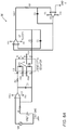
- Fig. 6A is a schematic representation of an electronic circuit 36 according to an embodiment of the present invention.
- Fig. 6A shows electronic circuit 36 using common electronic circuit notation.
- Typical values or types of the electronic components in electronic circuit 36 are given in Table 1, below, and those having ordinary skill in the art will be aware of variations in these values and types.
- Typical supply voltages of electronic circuit 36 are given in Table 2, below.
- Table 2 Supply voltage symbol Voltage +Vcc +5V -Vcc -5V +Vc +5V -Vc -5V
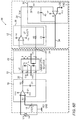
- Fig. 6B is a schematic representation of electronic circuit 36, with additional references to the functional elements of circuit 8 of Fig. 1 .
- the major functional circuit components, linear isolation amplifier 10 and transimpedance receiver 12, are outlined in broken lines in electronic circuit 36.
- the internal circuit components of isolation amplifier 10 and transimpedance receiver 12 - pre-amplifier 16, linear opto-isolator 22, operational amplifier circuit 26, and integrator 30 - are further outlined in broken lines within the major functional circuit components. Signals and reference voltages are labelled in accordance with Fig. 1 .
- Pre-amplifier 16 comprises an operational amplifier U1, where the voltage between the differential input terminals is the sum of the input AC-signal 14 (labelled VIN in circuit diagram 36) and reference DC-voltage 18 (labelled VREF in circuit diagram 36).
- a resistor R1 determines the forward current through a diode D1.
- a resistor R2 limits the maximum current value through diode D1 and an output capacitor C1 prevents potential parasitic oscillations.
- Operational amplifier circuit 26 comprises an operational amplifier U7, with a resistor R3 determining the output stage gain, and a capacitor C2 controlling its frequency behavior.
- Integrator 30 comprises an operational amplifier U2, as well as an input resistor 38 (R4) and a feedback capacitor 40 (C3), whose function will be described below.
- the combination of integrator 30 and operational amplifier circuit 26 functions as an AC coupling amplifier with a single-pole high-pass filter response.
- FIGs. 6A and 6B show a particular electronic configuration and choice of circuit components, by way of example, the principles of circuit 8 may alternatively be implemented using other circuit components and component values, as will be apparent to those skilled in the art. It will thus be appreciated that the embodiments described above are cited by way of example, and that the present invention is not limited to what has been particularly shown and described hereinabove. Rather, the scope of the present invention includes both combinations and subcombinations of the various features described hereinabove, as well as variations and modifications thereof which would occur to persons skilled in the art upon reading the foregoing description and which are not disclosed in the prior art.
Landscapes
- Engineering & Computer Science (AREA)
- Power Engineering (AREA)
- Physics & Mathematics (AREA)
- Electromagnetism (AREA)
- Computer Networks & Wireless Communication (AREA)
- Signal Processing (AREA)
- Amplifiers (AREA)
Abstract
Description
- The present invention relates generally to electronic circuits, and particularly to linear isolation amplifiers.
- It is commonly required that an electronic signal, either a voltage or current signal, be transmitted from one part of an electronic circuit to another part of the circuit, without any ohmic contact between the two parts. An example of such a case is provided by a circuit of which one part is in contact with a human, such as when a patient is monitored by one part of the circuit, and the other part is connected to external electronic equipment. Providing complete ohmic isolation between the two parts of the circuit ensures that an electronic malfunction in the external electronic equipment will not cause a harmful current to flow through the patient. A widely used electronic circuit for passing signals, while isolating the two parts of the circuit, is a linear isolation amplifier, based on a linear opto-coupler. The term "signal" is used in the present description and in the claims to denote an electronic voltage or current signal, unless otherwise specified.
- The linear opto-coupler transmits a signal through one or more pairs of an optical emitter and a receiver, so that the electronic signal is translated first into an optical signal and then back into an electronic signal. Due to the asymmetrical construction of the emitter-receiver pairs and the non-conducting (dielectric) gap transmitting the emitted photons, the signal will travel in one direction only, without any possibility of a reverse current flowing towards the patient. The use of a photonic circuit, however, imposes a condition of unipolarity on the transmitted signal. (For the sake of clarity, the following description refers to positive unipolar signals, as well as positive reference and threshold voltages, but negative unipolar signals, together with negative offset and threshold voltages, may be used in a similar fashion.) In addition to the requirement of positive unipolarity, due to the fact that photonic emitters exhibit linear behavior only above a threshold excitation above zero, the minimum value of the transmitted signal is generally set to be above this threshold.
- When the signal to be transmitted is a pure AC-signal, it is converted to a positive unipolar signal before being input to the linear opto-coupler. This conversion may be accomplished by a pre-amplifier within the linear isolation amplifier, which pre-amplifier adds a fixed, positive DC-reference voltage to the AC-signal, thus creating a positive unipolar signal with a sufficiently high positive minimum value. Once the positive unipolar signal has been passed through the linear opto-coupler, its AC-component can be recovered.
- Embodiments of the present invention that are described hereinbelow provide improved isolation circuits and a method for their use.
- There is therefore provided, in accordance with an embodiment of the present invention, an electronic circuit, including an isolation amplifier, having a first input terminal coupled to receive an input AC-signal and including a linear opto-isolator, which has a first output terminal and is coupled to provide at the first output terminal a unipolar signal, having an AC-component proportional to the input signal, and a transimpedance receiver, including a first operational amplifier, having a second output terminal and first and second differential input terminals, with the first differential input terminal coupled to receive and amplify the unipolar output signal from the first output terminal so as to provide an output signal from the circuit at the second output terminal, and a second operational amplifier, which is configured as an integrator, and which has a third output terminal coupled to the second differential input terminal and has third and fourth differential input terminals, with the third differential input terminal coupled to receive the output signal from the second output terminal and the fourth differential input terminal connected to a ground.
- In some embodiments, the transimpedance receiver includes an input resistor and a feedback capacitor coupled to the second operational amplifier, with values chosen so that the transimpedance receiver functions as an AC-coupling amplifier configured as a high-pass filter. In a disclosed embodiment, the high-pass filter is a single-pole high-pass filter.
- In a further disclosed embodiment, the output signal at the second output terminal has a zero DC-component.
- In still other embodiments, the isolation amplifier has a second input terminal coupled to receive a reference DC-voltage while the transimpedance receiver generates the output signal without using any reference DC-voltage.
- There is also provided, in accordance with an embodiment of the present invention, a method for producing an electronic circuit, the method including providing an isolation amplifier, having a first input terminal coupled to receive an input AC-signal and including a linear opto-isolator, which has a first output terminal and is coupled to provide at the first output terminal a unipolar signal, having an AC-component proportional to the input signal, and providing a transimpedance receiver, including a first operational amplifier, having a second output terminal and first and second differential input terminals, with the first differential input terminal coupled to receive and amplify the unipolar output signal from the first output terminal so as to provide an output signal from the circuit at the second output terminal, and a second operational amplifier, which is configured as an integrator, and which has a third output terminal coupled to the second differential input terminal and has third and fourth differential input terminals, with the third differential input terminal coupled to receive the output signal from the second output terminal and the fourth differential input terminal connected to a ground.
- There is additionally provided, in accordance with an embodiment of the present invention, a method, wherein the transimpedance receiver includes an input resistor and a feedback capacitor coupled to the second operational amplifier, with values chosen so that the transimpedance receiver functions as an AC-coupling amplifier configured as a high-pass filter.
- There is further provided, in accordance with an embodiment of the present invention, a method, wherein the high-pass filter is a single-pole high-pass filter.
- There is provided, in accordance with an embodiment of the present invention, a method, wherein the output signal at the second output terminal has a zero DC-component.
- There is further provided, in accordance with an embodiment of the present invention, a method, wherein the isolation amplifier has a second input terminal coupled to receive a reference DC-voltage while the transimpedance receiver generates the output signal without using any reference DC-voltage.
- The present invention will be more fully understood from the following detailed description of the embodiments thereof, taken together with the drawings in which:
-
-
Fig. 1 is a schematic block diagram of an electronic circuit, in accordance with an embodiment of the invention; -
Fig. 2 is a schematic diagram of an input AC-signal to a linear isolation amplifier, in accordance with an embodiment of the invention; -
Fig. 3 is a schematic diagram of a positive unipolar input signal to a linear opto-coupler, in accordance with an embodiment of the invention; -
Fig. 4 is a schematic diagram of a positive unipolar output signal from a linear opto-coupler, in accordance with an embodiment of the invention; -
Fig. 5 is a schematic diagram of an output signal from a transimpedance receiver, in accordance with an embodiment of the invention; and -
Figs. 6A-6B are diagrams of an electronic circuit, in accordance with an embodiment of the invention. - As noted earlier, in order for an AC-signal to be transmitted correctly by a linear opto-coupler that is part of a linear isolation amplifier, the AC-signal originating from a sensor is converted to a positive unipolar signal before presenting it as an input to the linear opto-coupler. This conversion is accomplished by adding to the AC-signal a positive DC offset voltage. The positive DC offset voltage is based on a reference DC-voltage on the input side of the linear opto-coupler. Due to the requirement of ohmic isolation between the input and output sides of the linear opto-coupler, this reference DC-voltage is not accessible at the output side of the linear opto-coupler. Once the positive unipolar signal has been transmitted to the output terminal of the linear isolation amplifier, the DC offset voltage is removed in order to recover the initial AC-signal. When a second reference DC-voltage is used for this purpose, any discrepancy between the reference voltages on the input and output sides of the isolation amplifier, such as a voltage difference or a time-dependent drift, will distort the recovered AC-signal by a residual DC-voltage offset.
- An embodiment of the present invention described herein circumvents the problem inherent in the use of two reference voltages by applying a method of high-pass filtering to the output signal from the linear isolation amplifier, without using any second reference DC-voltage. By choosing the frequency response of the high-pass filter appropriately, it will filter out the DC-voltage component of the output signal, while transmitting in an undistorted fashion the AC-component of the output signal.
- In some embodiments, the high-pass filtering is accomplished by a transimpedance receiver, which is configured as an AC-coupling amplifier. As will be described in detail below, the transimpedance receiver comprises an operational amplifier, wherein one of the differential input terminals of the operational amplifier receives the output signal from the linear isolation amplifier. The output terminal of the operational amplifier is connected to one of the differential input terminals of a second operational amplifier, which is configured as an integrator. The second differential input terminal of the integrator (second operational amplifier) is connected to ground potential. The output terminal of the integrator is connected to the second differential input terminal of the first operational amplifier, providing a negative feedback to this operational amplifier, and ensuring that the DC-component of the output signal of the first operational amplifier is always zero.
- Thus, the output signal of the first operational amplifier, with a zero DC-component, faithfully replicates the initial input AC-signal. As will be described in detail below, the design of the high-pass filter, and specifically that of the integrator, can be chosen in such a way that the act of filtering out the DC-component has no detrimental effect on the AC-signal. Specifically, when designing the high-pass filter as a single-pole filter, the position of the cut-off frequency can be chosen well below the frequency spectrum of the AC-signal, while still well above zero frequency (DC).
- This novel combination of a linear isolation amplifier and a transimpedance receiver, with the latter configured as a high-pass filter, is advantageous for transmitting AC-signals in an ohmically isolated way, since no second reference DC-voltage is required. In addition, the recovered AC-signal is free of distortion due to DC reference mismatch or temporal drift. Furthermore, an embodiment of the present invention may be applied to any linear isolation amplifier available from the manufacturers of such devices.
-
Fig. 1 is a schematic block diagram of anisolation circuit 8, in accordance with an embodiment of the present invention. The two major parts ofcircuit 8 are alinear isolation amplifier 10 and atransimpedance receiver 12, outlined by broken lines in this figure. An input AC-signal 14 is connected to an input terminal of a pre-amplifier 16 withinlinear isolation amplifier 10. In pre-amplifier 16, a positive reference DC-voltage 18 is added to input AC-signal 14, producing a positiveunipolar signal 20 at the output terminal of pre-amplifier 16.Signal 20 is used as an input to a linear opto-isolator 22 withinlinear isolation amplifier 10, and opto-isolator 22converts signal 20 to a positiveunipolar output signal 24, ohmically isolated fromsignal 20. -
Signal 24 forms an input signal totransimpedance receiver 12, wheresignal 24 is connected to a differential input terminal of anoperational amplifier circuit 26 withintransimpedance receiver 12.Operational amplifier circuit 26 forms anoutput signal 28, which is connected to a differential input terminal of anintegrator 30 withintransimpedance receiver 12. A second differential input terminal ofintegrator 30 is connected to ground potential via aconnection 32. Anoutput signal 34 ofintegrator 30 is connected to a second differential input terminal ofoperational amplifier circuit 26, providing negative feedback tooperational amplifier circuit 26, and ensuring thatoutput signal 28 has zero DC-component and thatoutput signal 28 recovers original input AC-signal 14. -
Figs. 2-5 are schematic representations of the signal voltages at various locations incircuit 8 ofFig. 1 , with additional references toFig. 1 . The horizontal axis represents time, and the vertical axis represents the voltage of a signal. -
Fig. 2 is a schematic representation of input AC-signal 14. Input AC-signal 14 has only an AC-component, with zero DC-component. -
Fig. 3 is a schematic representation of positiveunipolar signal 20, which is the output signal frompre-amplifier 16, after adding positive reference DC-voltage 18 to input AC-signal 14. The magnitude of positive reference DC-voltage 18 is denoted as VREF inFig. 3 . The minimum value of positiveunipolar signal 20, as required for proper functioning of linear opto-coupler 22, is denoted by VTH inFig. 3 . -
Fig. 4 is a schematic representation ofoutput signal 24 from linear opto-isolator 22. Assuming for the sake of simplicity a unity gain for linear opto-isolator 22,output signal 24 is an exact reproduction of positiveunipolar signal 20. -
Fig. 5 is a schematic representation ofoutput signal 28, wherein the DC-component present inoutput signal 24 has been removed due to thetransimpedance receiver 12 functioning as an AC-coupling amplifier, and wherein the remaining AC-component is a faithful reproduction of input AC-signal 14. -
Fig. 6A is a schematic representation of anelectronic circuit 36 according to an embodiment of the present invention. For the sake of clarity,Fig. 6A showselectronic circuit 36 using common electronic circuit notation. Typical values or types of the electronic components inelectronic circuit 36 are given in Table 1, below, and those having ordinary skill in the art will be aware of variations in these values and types.Table 1 Component Function Type/Value R1 Resistor 30.1kΩ U1 Operational amplifier TLV2371 C1 Capacitor 100pF R2 Resistor 604Ω U8 Linear opto-isolator IL300 U7 Operational amplifier TLV2371 R3 Resistor 30.1kΩ C2 Capacitor 100pF C3 Capacitor 10µF U2 Operational amplifier TLV2371 R4 Resistor 100kΩ - Typical supply voltages of
electronic circuit 36 are given in Table 2, below.Table 2 Supply voltage symbol Voltage +Vcc +5V -Vcc -5V +Vc +5V -Vc -5V - Additional explanations and clarifications of
electronic circuit 36 are given in the following figure,Fig. 6B . -
Fig. 6B is a schematic representation ofelectronic circuit 36, with additional references to the functional elements ofcircuit 8 ofFig. 1 . The major functional circuit components,linear isolation amplifier 10 andtransimpedance receiver 12, are outlined in broken lines inelectronic circuit 36. The internal circuit components ofisolation amplifier 10 and transimpedance receiver 12 -pre-amplifier 16, linear opto-isolator 22,operational amplifier circuit 26, and integrator 30 - are further outlined in broken lines within the major functional circuit components. Signals and reference voltages are labelled in accordance withFig. 1 . -
Pre-amplifier 16 comprises an operational amplifier U1, where the voltage between the differential input terminals is the sum of the input AC-signal 14 (labelled VIN in circuit diagram 36) and reference DC-voltage 18 (labelled VREF in circuit diagram 36). A resistor R1 determines the forward current through a diode D1. A resistor R2 limits the maximum current value through diode D1 and an output capacitor C1 prevents potential parasitic oscillations. -
Operational amplifier circuit 26 comprises an operational amplifier U7, with a resistor R3 determining the output stage gain, and a capacitor C2 controlling its frequency behavior.Integrator 30 comprises an operational amplifier U2, as well as an input resistor 38 (R4) and a feedback capacitor 40 (C3), whose function will be described below. The combination ofintegrator 30 andoperational amplifier circuit 26 functions as an AC coupling amplifier with a single-pole high-pass filter response. - The functional characteristics of
integrator 30 are controlled byresistor 38 andcapacitor 40. Denoting the values of these components, in accordance with the drawing ofelectronic circuit 36, by R4 forresistor 38 and by C3 forcapacitor 40, the cut-off frequency fCUTOFF of the high-pass filter can be calculated to be
- When the cut-off frequency fCUTOFF is chosen so that it is well below the frequency spectrum of input AC-
signal 14, while still being well above zero frequency (DC), input AC-signal 14 will be faithfully reproduced atoutput signal 28, without any residual DC-signal. - Although
Figs. 6A and6B show a particular electronic configuration and choice of circuit components, by way of example, the principles ofcircuit 8 may alternatively be implemented using other circuit components and component values, as will be apparent to those skilled in the art. It will thus be appreciated that the embodiments described above are cited by way of example, and that the present invention is not limited to what has been particularly shown and described hereinabove. Rather, the scope of the present invention includes both combinations and subcombinations of the various features described hereinabove, as well as variations and modifications thereof which would occur to persons skilled in the art upon reading the foregoing description and which are not disclosed in the prior art.
Claims (10)
- An electronic circuit, comprising:an isolation amplifier, having a first input terminal coupled to receive an input AC-signal and comprising a linear opto-isolator, which has a first output terminal and is coupled to provide at the first output terminal a unipolar signal, having an AC-component proportional to the input signal; anda transimpedance receiver, comprising:a first operational amplifier, having a second output terminal and first and second differential input terminals, with the first differential input terminal coupled to receive and amplify the unipolar output signal from the first output terminal so as to provide an output signal from the circuit at the second output terminal; anda second operational amplifier, which is configured as an integrator, and which has a third output terminal coupled to the second differential input terminal and has third and fourth differential input terminals, with the third differential input terminal coupled to receive the output signal from the second output terminal and the fourth differential input terminal connected to a ground.
- The electronic circuit according to claim 1, wherein the transimpedance receiver comprises an input resistor and a feedback capacitor coupled to the second operational amplifier, with values chosen so that the transimpedance receiver functions as an AC-coupling amplifier configured as a high-pass filter.
- The electronic circuit according to claim 2, wherein the high-pass filter comprises a single-pole high-pass filter.
- The electronic circuit according to claim 1, wherein the output signal at the second output terminal has a zero DC-component.
- The electronic circuit according to claim 1, wherein the isolation amplifier has a second input terminal coupled to receive a reference DC-voltage while the transimpedance receiver generates the output signal without using any reference DC-voltage.
- A method for producing an electronic circuit, the method comprising:providing an isolation amplifier, having a first input terminal coupled to receive an input AC-signal and comprising a linear opto-isolator, which has a first output terminal and is coupled to provide at the first output terminal a unipolar signal, having an AC-component proportional to the input signal; andproviding a transimpedance receiver, comprising:a first operational amplifier, having a second output terminal and first and second differential input terminals, with the first differential input terminal coupled to receive and amplify the unipolar output signal from the first output terminal so as to provide an output signal from the circuit at the second output terminal; anda second operational amplifier, which is configured as an integrator, and which has a third output terminal coupled to the second differential input terminal and has third and fourth differential input terminals, with the third differential input terminal coupled to receive the output signal from the second output terminal and the fourth differential input terminal connected to a ground.
- The method according to claim 6, wherein the transimpedance receiver comprises an input resistor and a feedback capacitor coupled to the second operational amplifier, with values chosen so that the transimpedance receiver functions as an AC-coupling amplifier configured as a high-pass filter.
- The method according to claim 7, wherein the high-pass filter comprises a single-pole high-pass filter.
- The method according to claim 6, wherein the output signal at the second output terminal has a zero DC-component.
- The method according to claim 6, wherein the isolation amplifier has a second input terminal coupled to receive a reference DC-voltage while the transimpedance receiver generates the output signal without using any reference DC-voltage.
Applications Claiming Priority (1)
| Application Number | Priority Date | Filing Date | Title |
|---|---|---|---|
| US15/089,703 US10044447B2 (en) | 2016-04-04 | 2016-04-04 | Linear isolation amplifier with output DC voltage cancellation |
Publications (1)
| Publication Number | Publication Date |
|---|---|
| EP3255790A1 true EP3255790A1 (en) | 2017-12-13 |
Family
ID=58347212
Family Applications (1)
| Application Number | Title | Priority Date | Filing Date |
|---|---|---|---|
| EP17161108.0A Withdrawn EP3255790A1 (en) | 2016-04-04 | 2017-03-15 | Linear isolation amplifier with output dc voltage cancellation |
Country Status (7)
| Country | Link |
|---|---|
| US (1) | US10044447B2 (en) |
| EP (1) | EP3255790A1 (en) |
| JP (1) | JP2017188898A (en) |
| CN (1) | CN107276545A (en) |
| AU (1) | AU2017201703A1 (en) |
| CA (1) | CA2962245A1 (en) |
| IL (1) | IL251251B (en) |
Families Citing this family (3)
| Publication number | Priority date | Publication date | Assignee | Title |
|---|---|---|---|---|
| US10044447B2 (en) * | 2016-04-04 | 2018-08-07 | Biosense Webster (Israel) Ltd. | Linear isolation amplifier with output DC voltage cancellation |
| US10911006B2 (en) * | 2019-03-15 | 2021-02-02 | Littelfuse, Inc. | Linear isolation amplifier and method for self-calibration thereof |
| CN112971810B (en) * | 2021-05-11 | 2021-08-10 | 浙江普可医疗科技有限公司 | Electroencephalogram acquisition system |
Citations (5)
| Publication number | Priority date | Publication date | Assignee | Title |
|---|---|---|---|---|
| JPH02193402A (en) * | 1989-01-20 | 1990-07-31 | Sharp Corp | Optical coupling element |
| EP0480182A2 (en) * | 1990-10-09 | 1992-04-15 | International Business Machines Corporation | Noise cancelling circuitry for optical systems |
| US5278515A (en) * | 1992-12-24 | 1994-01-11 | Uniphase Corporation | High bandwidth information channel with optocoupling isolation |
| WO2011109770A2 (en) * | 2010-03-05 | 2011-09-09 | Gtran Inc. | Burst mode amplifier |
| US20120241599A1 (en) * | 2011-03-23 | 2012-09-27 | Kabushiki Kaisha Toshiba | Voltage output circuit, connector module, and active cable |
Family Cites Families (35)
| Publication number | Priority date | Publication date | Assignee | Title |
|---|---|---|---|---|
| US3893037A (en) * | 1973-09-09 | 1975-07-01 | William L Herbert | Isolating linear amplifier |
| US4078156A (en) | 1977-01-03 | 1978-03-07 | Avco Corporation | Drift cancellation circuit for multiplexer amplifier |
| CA1151314A (en) | 1978-09-15 | 1983-08-02 | Robert R. Lafrance | X-ray system signal derivation circuits for heat unit indicators and/or calibration meters |
| JPS5596708A (en) * | 1979-01-19 | 1980-07-23 | Oki Electric Ind Co Ltd | Isolation amplifier circuit |
| US4313225A (en) * | 1979-11-05 | 1982-01-26 | Bell Telephone Laboratories, Incorporated | Opto-isolator hybrid circuit |
| GB2071435A (en) * | 1980-02-27 | 1981-09-16 | Data Beta Ltd | Electrical power supplies |
| US4385286A (en) | 1980-07-18 | 1983-05-24 | American Microsystems, Inc. | Use of single reference voltage for analog to digital or digital to analog conversion of bipolar signals |
| US4546262A (en) * | 1983-06-27 | 1985-10-08 | Xerox Corporation | Isolated high voltage controller |
| US4536715A (en) * | 1983-12-05 | 1985-08-20 | At&T Bell Laboratories | Linear dual detector opto-isolator circuit |
| US4591800A (en) | 1984-10-01 | 1986-05-27 | Motorola, Inc. | Linear power amplifier feedback improvement |
| JPH02134005A (en) * | 1988-11-15 | 1990-05-23 | Meidensha Corp | Dc amplifier |
| JP2516706B2 (en) * | 1990-11-24 | 1996-07-24 | ローム株式会社 | Amplifier |
| US5245654A (en) * | 1991-10-10 | 1993-09-14 | Cermetek Microelectronics, Inc. | Solid state isolation device using opto-isolators |
| US5760939A (en) * | 1995-10-23 | 1998-06-02 | Sdl, Inc. | Optical transmission link capable of high temperature operation without cooling with an optical receiver module having temperature independent sensitivity performance and optical transmitter module with laser diode source |
| US6188276B1 (en) | 1998-09-21 | 2001-02-13 | Anastasios V. Simopoulos | Power amplifier |
| US6181264B1 (en) | 1999-05-18 | 2001-01-30 | Agilent Technologies | Precision bipolar digital-to-analog converter for an instrument probe interface |
| US6717474B2 (en) * | 2002-01-28 | 2004-04-06 | Integrated Programmable Communications, Inc. | High-speed differential to single-ended converter |
| US6956439B1 (en) * | 2003-12-12 | 2005-10-18 | National Semiconductor Corporation | Transimpedance amplifier with controllable noise reduction |
| US7394995B2 (en) * | 2004-04-01 | 2008-07-01 | Avanex Corporation | System and method for a compact optical receiver with wide dynamic range |
| US7532065B2 (en) * | 2005-07-12 | 2009-05-12 | Agere Systems Inc. | Analog amplifier having DC offset cancellation circuit and method of offset cancellation for analog amplifiers |
| US7813885B2 (en) * | 2006-01-20 | 2010-10-12 | Carrier Corporation | Method and apparatus for measurement of AC voltages in an HVAC system |
| MY155262A (en) * | 2007-03-12 | 2015-09-30 | Oyl Res And Dev Ct Sdn Bhd | A conversion circuit |
| JP5304642B2 (en) * | 2007-03-29 | 2013-10-02 | 日本電気株式会社 | Signal amplifier for optical receiver circuit |
| US8116055B2 (en) * | 2007-06-21 | 2012-02-14 | Avago Technologies Ecbu Ip (Singapore) Pte. Ltd. | Methods and apparatuses for performing common mode pulse compensation in an opto-isolator |
| US7865164B2 (en) * | 2007-09-27 | 2011-01-04 | Qualcomm Incorporated | Apparatus and methods for downconverting radio frequency signals |
| CN101931376A (en) * | 2009-06-23 | 2010-12-29 | 骅讯电子企业股份有限公司 | DC isolation amplifier |
| GB0916762D0 (en) * | 2009-09-24 | 2009-11-04 | Gigle Semiconductor Ltd | Electrical isolators |
| GB2485620B (en) * | 2010-12-16 | 2013-04-17 | Wolfson Microelectronics Plc | DC offset compensation |
| US8461922B2 (en) * | 2011-02-24 | 2013-06-11 | Lsi Corporation | Offset component cancelation method and circuit |
| US9190966B2 (en) * | 2012-05-22 | 2015-11-17 | Stryker Corporation | Impedance bootstrap circuit for an interface of a monitoring device |
| CN102664621B (en) * | 2012-05-25 | 2014-08-13 | 长园深瑞继保自动化有限公司 | Isolation method and circuit for signal acquisition of electronic mutual inductor |
| US9490802B2 (en) * | 2012-10-23 | 2016-11-08 | Abb Technology Ltd. | Apparatus and method for transmitting an analog signal, and analog signal multiplexer |
| US8983304B2 (en) * | 2012-10-25 | 2015-03-17 | Avago Technologies General Ip (Singapore) Pte. Ltd. | Opto-isolator with compensation circuit |
| US9484913B2 (en) * | 2014-03-11 | 2016-11-01 | Texas Instruments Incorporated | Emulation of LED input characteristics in BICMOS process |
| US10044447B2 (en) * | 2016-04-04 | 2018-08-07 | Biosense Webster (Israel) Ltd. | Linear isolation amplifier with output DC voltage cancellation |
-
2016
- 2016-04-04 US US15/089,703 patent/US10044447B2/en not_active Expired - Fee Related
-
2017
- 2017-03-13 AU AU2017201703A patent/AU2017201703A1/en not_active Abandoned
- 2017-03-15 EP EP17161108.0A patent/EP3255790A1/en not_active Withdrawn
- 2017-03-19 IL IL251251A patent/IL251251B/en active IP Right Grant
- 2017-03-27 CA CA2962245A patent/CA2962245A1/en not_active Abandoned
- 2017-03-31 CN CN201710206476.4A patent/CN107276545A/en active Pending
- 2017-04-03 JP JP2017073504A patent/JP2017188898A/en active Pending
Patent Citations (5)
| Publication number | Priority date | Publication date | Assignee | Title |
|---|---|---|---|---|
| JPH02193402A (en) * | 1989-01-20 | 1990-07-31 | Sharp Corp | Optical coupling element |
| EP0480182A2 (en) * | 1990-10-09 | 1992-04-15 | International Business Machines Corporation | Noise cancelling circuitry for optical systems |
| US5278515A (en) * | 1992-12-24 | 1994-01-11 | Uniphase Corporation | High bandwidth information channel with optocoupling isolation |
| WO2011109770A2 (en) * | 2010-03-05 | 2011-09-09 | Gtran Inc. | Burst mode amplifier |
| US20120241599A1 (en) * | 2011-03-23 | 2012-09-27 | Kabushiki Kaisha Toshiba | Voltage output circuit, connector module, and active cable |
Also Published As
| Publication number | Publication date |
|---|---|
| US20170288785A1 (en) | 2017-10-05 |
| CA2962245A1 (en) | 2017-10-04 |
| US10044447B2 (en) | 2018-08-07 |
| IL251251A0 (en) | 2017-06-29 |
| IL251251B (en) | 2020-01-30 |
| JP2017188898A (en) | 2017-10-12 |
| AU2017201703A1 (en) | 2017-10-19 |
| CN107276545A (en) | 2017-10-20 |
Similar Documents
| Publication | Publication Date | Title |
|---|---|---|
| US7368999B2 (en) | DC offset cancellation for a trans-impedance amplifier | |
| US20200091881A1 (en) | Differential trans-impedance amplifier | |
| US20130057348A1 (en) | Transimpedance Amplifier | |
| CN114050818A (en) | Digital isolators and chips | |
| US6876259B2 (en) | Fully integrated received signal strength indicator for a transimpedance amplifier | |
| US10044447B2 (en) | Linear isolation amplifier with output DC voltage cancellation | |
| US11349444B2 (en) | Transimpedance amplifier circuit | |
| US20140049323A1 (en) | Transimpedance amplifier | |
| JPWO2008120663A1 (en) | Signal amplifier for optical receiver circuit | |
| US20080240735A1 (en) | Symmetrical Optical Receiver | |
| US6844784B1 (en) | Wide dynamic range transimpedance amplifier | |
| US11411542B2 (en) | Transimpedance amplifier circuit | |
| CN106452381A (en) | Coupling-capacitance-free instrument amplifier with direct current offset inhibition function and implementation method thereof | |
| JP3404209B2 (en) | Transimpedance amplifier circuit | |
| EP0828344A2 (en) | Integrated circuit and method for generating a transimpedance function | |
| US4975566A (en) | First stage circuit for an optical receiver | |
| JPS62139403A (en) | optical receiver | |
| CN103900686B (en) | A kind of preamplifying circuit for high-speed photodetector | |
| JPH04225611A (en) | Wide dynamic range light receiving circuit | |
| JP7251388B2 (en) | Transimpedance amplifier circuit | |
| JP7259625B2 (en) | Transimpedance amplifier circuit | |
| EP4216429A1 (en) | A transimpedance amplifier | |
| KR20240111298A (en) | Offset reduction for silicon microphones | |
| SU1676065A1 (en) | Operational amplifiers based on cmos transistors | |
| US2197346A (en) | Detector-amplifier circuit arrangement |
Legal Events
| Date | Code | Title | Description |
|---|---|---|---|
| PUAI | Public reference made under article 153(3) epc to a published international application that has entered the european phase |
Free format text: ORIGINAL CODE: 0009012 |
|
| STAA | Information on the status of an ep patent application or granted ep patent |
Free format text: STATUS: THE APPLICATION HAS BEEN PUBLISHED |
|
| AK | Designated contracting states |
Kind code of ref document: A1 Designated state(s): AL AT BE BG CH CY CZ DE DK EE ES FI FR GB GR HR HU IE IS IT LI LT LU LV MC MK MT NL NO PL PT RO RS SE SI SK SM TR |
|
| AX | Request for extension of the european patent |
Extension state: BA ME |
|
| STAA | Information on the status of an ep patent application or granted ep patent |
Free format text: STATUS: REQUEST FOR EXAMINATION WAS MADE |
|
| 17P | Request for examination filed |
Effective date: 20180613 |
|
| RBV | Designated contracting states (corrected) |
Designated state(s): AL AT BE BG CH CY CZ DE DK EE ES FI FR GB GR HR HU IE IS IT LI LT LU LV MC MK MT NL NO PL PT RO RS SE SI SK SM TR |
|
| STAA | Information on the status of an ep patent application or granted ep patent |
Free format text: STATUS: EXAMINATION IS IN PROGRESS |
|
| 17Q | First examination report despatched |
Effective date: 20191031 |
|
| STAA | Information on the status of an ep patent application or granted ep patent |
Free format text: STATUS: THE APPLICATION IS DEEMED TO BE WITHDRAWN |
|
| 18D | Application deemed to be withdrawn |
Effective date: 20211123 |