EP3255667A1 - Semiconductor device and lead frame therefor - Google Patents
Semiconductor device and lead frame therefor Download PDFInfo
- Publication number
- EP3255667A1 EP3255667A1 EP17165110.2A EP17165110A EP3255667A1 EP 3255667 A1 EP3255667 A1 EP 3255667A1 EP 17165110 A EP17165110 A EP 17165110A EP 3255667 A1 EP3255667 A1 EP 3255667A1
- Authority
- EP
- European Patent Office
- Prior art keywords
- lead frame
- branch
- semiconductor device
- terminal
- semiconductor die
- Prior art date
- Legal status (The legal status is an assumption and is not a legal conclusion. Google has not performed a legal analysis and makes no representation as to the accuracy of the status listed.)
- Pending
Links
Images




Classifications
-
- H—ELECTRICITY
- H10—SEMICONDUCTOR DEVICES; ELECTRIC SOLID-STATE DEVICES NOT OTHERWISE PROVIDED FOR
- H10W—GENERIC PACKAGES, INTERCONNECTIONS, CONNECTORS OR OTHER CONSTRUCTIONAL DETAILS OF DEVICES COVERED BY CLASS H10
- H10W70/00—Package substrates; Interposers; Redistribution layers [RDL]
- H10W70/40—Leadframes
- H10W70/464—Additional interconnections in combination with leadframes
- H10W70/465—Bumps or wires
-
- H—ELECTRICITY
- H10—SEMICONDUCTOR DEVICES; ELECTRIC SOLID-STATE DEVICES NOT OTHERWISE PROVIDED FOR
- H10W—GENERIC PACKAGES, INTERCONNECTIONS, CONNECTORS OR OTHER CONSTRUCTIONAL DETAILS OF DEVICES COVERED BY CLASS H10
- H10W40/00—Arrangements for thermal protection or thermal control
- H10W40/20—Arrangements for cooling
- H10W40/22—Arrangements for cooling characterised by their shape, e.g. having conical or cylindrical projections
-
- H—ELECTRICITY
- H05—ELECTRIC TECHNIQUES NOT OTHERWISE PROVIDED FOR
- H05K—PRINTED CIRCUITS; CASINGS OR CONSTRUCTIONAL DETAILS OF ELECTRIC APPARATUS; MANUFACTURE OF ASSEMBLAGES OF ELECTRICAL COMPONENTS
- H05K1/00—Printed circuits
- H05K1/02—Details
- H05K1/0201—Thermal arrangements, e.g. for cooling, heating or preventing overheating
- H05K1/0203—Cooling of mounted components
- H05K1/0204—Cooling of mounted components using means for thermal conduction connection in the thickness direction of the substrate
-
- H—ELECTRICITY
- H05—ELECTRIC TECHNIQUES NOT OTHERWISE PROVIDED FOR
- H05K—PRINTED CIRCUITS; CASINGS OR CONSTRUCTIONAL DETAILS OF ELECTRIC APPARATUS; MANUFACTURE OF ASSEMBLAGES OF ELECTRICAL COMPONENTS
- H05K1/00—Printed circuits
- H05K1/02—Details
- H05K1/0201—Thermal arrangements, e.g. for cooling, heating or preventing overheating
- H05K1/0203—Cooling of mounted components
- H05K1/0207—Cooling of mounted components using internal conductor planes parallel to the surface for thermal conduction, e.g. power planes
-
- H—ELECTRICITY
- H05—ELECTRIC TECHNIQUES NOT OTHERWISE PROVIDED FOR
- H05K—PRINTED CIRCUITS; CASINGS OR CONSTRUCTIONAL DETAILS OF ELECTRIC APPARATUS; MANUFACTURE OF ASSEMBLAGES OF ELECTRICAL COMPONENTS
- H05K1/00—Printed circuits
- H05K1/02—Details
- H05K1/0201—Thermal arrangements, e.g. for cooling, heating or preventing overheating
- H05K1/0203—Cooling of mounted components
- H05K1/0209—External configuration of printed circuit board adapted for heat dissipation, e.g. lay-out of conductors, coatings
-
- H—ELECTRICITY
- H05—ELECTRIC TECHNIQUES NOT OTHERWISE PROVIDED FOR
- H05K—PRINTED CIRCUITS; CASINGS OR CONSTRUCTIONAL DETAILS OF ELECTRIC APPARATUS; MANUFACTURE OF ASSEMBLAGES OF ELECTRICAL COMPONENTS
- H05K7/00—Constructional details common to different types of electric apparatus
- H05K7/02—Arrangements of circuit components or wiring on supporting structure
- H05K7/10—Plug-in assemblages of components, e.g. IC sockets
-
- H—ELECTRICITY
- H05—ELECTRIC TECHNIQUES NOT OTHERWISE PROVIDED FOR
- H05K—PRINTED CIRCUITS; CASINGS OR CONSTRUCTIONAL DETAILS OF ELECTRIC APPARATUS; MANUFACTURE OF ASSEMBLAGES OF ELECTRICAL COMPONENTS
- H05K7/00—Constructional details common to different types of electric apparatus
- H05K7/20—Modifications to facilitate cooling, ventilating, or heating
- H05K7/2089—Modifications to facilitate cooling, ventilating, or heating for power electronics, e.g. for inverters for controlling motor
- H05K7/209—Heat transfer by conduction from internal heat source to heat radiating structure
-
- H—ELECTRICITY
- H10—SEMICONDUCTOR DEVICES; ELECTRIC SOLID-STATE DEVICES NOT OTHERWISE PROVIDED FOR
- H10W—GENERIC PACKAGES, INTERCONNECTIONS, CONNECTORS OR OTHER CONSTRUCTIONAL DETAILS OF DEVICES COVERED BY CLASS H10
- H10W40/00—Arrangements for thermal protection or thermal control
- H10W40/20—Arrangements for cooling
- H10W40/25—Arrangements for cooling characterised by their materials
-
- H—ELECTRICITY
- H10—SEMICONDUCTOR DEVICES; ELECTRIC SOLID-STATE DEVICES NOT OTHERWISE PROVIDED FOR
- H10W—GENERIC PACKAGES, INTERCONNECTIONS, CONNECTORS OR OTHER CONSTRUCTIONAL DETAILS OF DEVICES COVERED BY CLASS H10
- H10W70/00—Package substrates; Interposers; Redistribution layers [RDL]
- H10W70/40—Leadframes
- H10W70/421—Shapes or dispositions
- H10W70/424—Cross-sectional shapes
-
- H—ELECTRICITY
- H10—SEMICONDUCTOR DEVICES; ELECTRIC SOLID-STATE DEVICES NOT OTHERWISE PROVIDED FOR
- H10W—GENERIC PACKAGES, INTERCONNECTIONS, CONNECTORS OR OTHER CONSTRUCTIONAL DETAILS OF DEVICES COVERED BY CLASS H10
- H10W70/00—Package substrates; Interposers; Redistribution layers [RDL]
- H10W70/40—Leadframes
- H10W70/421—Shapes or dispositions
- H10W70/424—Cross-sectional shapes
- H10W70/427—Bent parts
-
- H—ELECTRICITY
- H10—SEMICONDUCTOR DEVICES; ELECTRIC SOLID-STATE DEVICES NOT OTHERWISE PROVIDED FOR
- H10W—GENERIC PACKAGES, INTERCONNECTIONS, CONNECTORS OR OTHER CONSTRUCTIONAL DETAILS OF DEVICES COVERED BY CLASS H10
- H10W70/00—Package substrates; Interposers; Redistribution layers [RDL]
- H10W70/40—Leadframes
- H10W70/481—Leadframes for devices being provided for in groups H10D8/00 - H10D48/00
-
- H—ELECTRICITY
- H10—SEMICONDUCTOR DEVICES; ELECTRIC SOLID-STATE DEVICES NOT OTHERWISE PROVIDED FOR
- H10W—GENERIC PACKAGES, INTERCONNECTIONS, CONNECTORS OR OTHER CONSTRUCTIONAL DETAILS OF DEVICES COVERED BY CLASS H10
- H10W72/00—Interconnections or connectors in packages
-
- H—ELECTRICITY
- H10—SEMICONDUCTOR DEVICES; ELECTRIC SOLID-STATE DEVICES NOT OTHERWISE PROVIDED FOR
- H10W—GENERIC PACKAGES, INTERCONNECTIONS, CONNECTORS OR OTHER CONSTRUCTIONAL DETAILS OF DEVICES COVERED BY CLASS H10
- H10W74/00—Encapsulations, e.g. protective coatings
- H10W74/01—Manufacture or treatment
-
- H—ELECTRICITY
- H10—SEMICONDUCTOR DEVICES; ELECTRIC SOLID-STATE DEVICES NOT OTHERWISE PROVIDED FOR
- H10W—GENERIC PACKAGES, INTERCONNECTIONS, CONNECTORS OR OTHER CONSTRUCTIONAL DETAILS OF DEVICES COVERED BY CLASS H10
- H10W74/00—Encapsulations, e.g. protective coatings
- H10W74/01—Manufacture or treatment
- H10W74/014—Manufacture or treatment using batch processing
-
- H—ELECTRICITY
- H10—SEMICONDUCTOR DEVICES; ELECTRIC SOLID-STATE DEVICES NOT OTHERWISE PROVIDED FOR
- H10W—GENERIC PACKAGES, INTERCONNECTIONS, CONNECTORS OR OTHER CONSTRUCTIONAL DETAILS OF DEVICES COVERED BY CLASS H10
- H10W72/00—Interconnections or connectors in packages
- H10W72/20—Bump connectors, e.g. solder bumps or copper pillars; Dummy bumps; Thermal bumps
- H10W72/251—Materials
- H10W72/252—Materials comprising solid metals or solid metalloids, e.g. PbSn, Ag or Cu
-
- H—ELECTRICITY
- H10—SEMICONDUCTOR DEVICES; ELECTRIC SOLID-STATE DEVICES NOT OTHERWISE PROVIDED FOR
- H10W—GENERIC PACKAGES, INTERCONNECTIONS, CONNECTORS OR OTHER CONSTRUCTIONAL DETAILS OF DEVICES COVERED BY CLASS H10
- H10W72/00—Interconnections or connectors in packages
- H10W72/30—Die-attach connectors
- H10W72/351—Materials of die-attach connectors
- H10W72/352—Materials of die-attach connectors comprising metals or metalloids, e.g. solders
-
- H—ELECTRICITY
- H10—SEMICONDUCTOR DEVICES; ELECTRIC SOLID-STATE DEVICES NOT OTHERWISE PROVIDED FOR
- H10W—GENERIC PACKAGES, INTERCONNECTIONS, CONNECTORS OR OTHER CONSTRUCTIONAL DETAILS OF DEVICES COVERED BY CLASS H10
- H10W72/00—Interconnections or connectors in packages
- H10W72/851—Dispositions of multiple connectors or interconnections
- H10W72/874—On different surfaces
- H10W72/877—Bump connectors and die-attach connectors
-
- H—ELECTRICITY
- H10—SEMICONDUCTOR DEVICES; ELECTRIC SOLID-STATE DEVICES NOT OTHERWISE PROVIDED FOR
- H10W—GENERIC PACKAGES, INTERCONNECTIONS, CONNECTORS OR OTHER CONSTRUCTIONAL DETAILS OF DEVICES COVERED BY CLASS H10
- H10W74/00—Encapsulations, e.g. protective coatings
- H10W74/10—Encapsulations, e.g. protective coatings characterised by their shape or disposition
- H10W74/131—Encapsulations, e.g. protective coatings characterised by their shape or disposition the semiconductor body being only partially enclosed
- H10W74/142—Encapsulations, e.g. protective coatings characterised by their shape or disposition the semiconductor body being only partially enclosed the encapsulations exposing the passive side of the semiconductor body
-
- H—ELECTRICITY
- H10—SEMICONDUCTOR DEVICES; ELECTRIC SOLID-STATE DEVICES NOT OTHERWISE PROVIDED FOR
- H10W—GENERIC PACKAGES, INTERCONNECTIONS, CONNECTORS OR OTHER CONSTRUCTIONAL DETAILS OF DEVICES COVERED BY CLASS H10
- H10W90/00—Package configurations
- H10W90/701—Package configurations characterised by the relative positions of pads or connectors relative to package parts
- H10W90/721—Package configurations characterised by the relative positions of pads or connectors relative to package parts of bump connectors
- H10W90/726—Package configurations characterised by the relative positions of pads or connectors relative to package parts of bump connectors between a chip and a stacked lead frame, conducting package substrate or heat sink
-
- H—ELECTRICITY
- H10—SEMICONDUCTOR DEVICES; ELECTRIC SOLID-STATE DEVICES NOT OTHERWISE PROVIDED FOR
- H10W—GENERIC PACKAGES, INTERCONNECTIONS, CONNECTORS OR OTHER CONSTRUCTIONAL DETAILS OF DEVICES COVERED BY CLASS H10
- H10W90/00—Package configurations
- H10W90/701—Package configurations characterised by the relative positions of pads or connectors relative to package parts
- H10W90/731—Package configurations characterised by the relative positions of pads or connectors relative to package parts of die-attach connectors
- H10W90/734—Package configurations characterised by the relative positions of pads or connectors relative to package parts of die-attach connectors between a chip and a stacked insulating package substrate, interposer or RDL
Definitions
- the present invention is directed to semiconductor devices and lead frames for semiconductor devices, and more particularly to compact lead frame based semiconductor package.
- Power devices such as power MOSFETs, require high performance thermal capacity and heat dissipation because they are required to drain unwanted large currents to ground or other rails to protect devices connected thereto from being damaged.
- the power devices face challenges from structural compactness, which requires them to have a very small footprint and package height.
- the present invention provides a semiconductor device, comprising a semiconductor die having a first side and an opposite second side, the semiconductor die comprising a first terminal on the first side and at least two second terminals on the second side, and a lead frame.
- the lead frame comprises first and second base parts that are mutually spaced from each other both electrically and mechanically, wherein the second side of the semiconductor die is mounted to the lead frame such that the at least two second terminals are electrically connected, respectively, to the first and second base parts.
- the lead frame further comprises first and second protrusions on the first and second base parts that project past a side of the die and provide first and second terminal surfaces that are co-planar with the first terminal on the first side of the semiconductor die.
- the present invention provides a semiconductor device, comprising a semiconductor die having a first terminal on a first side and at least two second terminals on an opposite second side, and a lead frame having first and second parts.
- Each of the first and second parts comprises a base and a protrusion.
- the protrusions are respectively connected to and protrude from first sides of the bases.
- a height of the protrusions is substantially equal to a thickness of the semiconductor die, such that when the semiconductor die is mounted on the lead frame with the second side of the die facing the bases of the first and second parts of the lead frame, then the first side of the die is co-planar with distal ends of the protrusions.
- a semiconductor device comprising: a semiconductor die comprising a first terminal on a first side and at least two second terminals on an opposite second side; and a lead frame comprising a first part and a second part, each of the first and second parts comprising a base and a protrusion, wherein the protrusions are respectively connected to and protrude from first sides of the bases, and wherein a height of the protrusions is substantially equal to a thickness of the semiconductor die, such that when the semiconductor die is mounted on the lead frame with the second side of the die facing the bases of the first and second parts of the lead frame, then the first side of the die is co-planar with distal ends of the protrusions.
- Each of the bases of the first part and second parts of the lead frame is connected to a corresponding one of the two second terminals of the semiconductor die.
- the distal ends of the protrusions and the first terminal are exposed on a bottom surface of the semiconductor device.
- Each of the bases of the first and second parts have second sides opposite to the first sides, wherein the second sides are exposed on a top surface of the semiconductor device. Sidewalls of the protrusions are exposed on a lateral sidewall of the semiconductor device.
- a molding compound may at least partially encapsulate the semiconductor die.
- the present invention further provides a lead frame for a semiconductor device.
- the lead frame comprises a first part including a first branch and a second branch, wherein the second branch is connected to and extends from the first branch.
- the lead frame also includes a second part having a third branch and a fourth branch, wherein the fourth branch is connected to and extends from the third branch.
- a first connection bar connects the first branch of the first part to the third branch of the second part of a neighboring lead frame when the lead frame is part of a matrix of lead frames.
- a second connection bar connects the first branch of the first part to the second and fourth branches respectively of the first and second parts of another neighboring lead frame.
- the second branch of the first part and the fourth branch of the second part extend in the same direction and to the same height.
- FIG. 1 is a perspective view of a semiconductor device 30 in accordance with an embodiment.
- the semiconductor device 30 has a top surface 302 and an opposing bottom surface 304.
- the semiconductor device 304 includes multiple contacts 306, 308, and 310.
- the contacts 306, 308, and 310 are used for electrically connecting the semiconductor device 30 to external circuit components, such as a printed circuit board (PCB).
- PCB printed circuit board
- the first contact 306 is exposed only on the bottom surface 304, while the second and third contacts 308, 310 extend from the bottom surface 304 to a lateral side wall 312 of the semiconductor device 30 where they also are exposed.
- the first contact 306 is provided on a conductive surface of a semiconductor die of the semiconductor device 30, while the second and the third contacts 308, 310 are provided by a conductive lead frame to which the die is mounted and electrically connected.
- the semiconductor die is a VDMOS
- the first contact 306 is connected to a drain of the VDMOS
- the second and third contacts 308, 310 are respectively connected to a source and a gate of the VDMOS.
- the semiconductor device 30 may be square or rectangular in shape, with a side length of 0.6mm, and a thickness of 0.4mm.
- the semiconductor die can be provided as BJT, thyristor, etc .
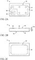
- FIGS. 2A and 2B a top plan view and a side view of a semiconductor die 32 of the semiconductor device 30 are illustrated.
- the semiconductor die 32 is generally rectangular shaped.
- a major portion on a first surface 322 is provided as a first terminal 324, and the other portion on the first surface 322 is provided as a second terminal 326.
- a third terminal is provided on an opposite second surface of the semiconductor die 32.
- the first and second terminals 324 and 326 provide the contacts 310 and 308, while the third terminal provides the contact 306.
- the relative proportion of the first terminal 324 and the second terminal 326 is not limited to that illustrated in FIG. 2A .
- the second terminal 326 may have an area equal to or larger than that of the first terminal 324.
- a length of the semiconductor die 32 is 0.5mm, and a width is 0.275mm.
- studs 328 are disposed on the first surface 322. As illustrated in FIG. 2B , the studs 328 are placed on top of the first surface 322, and with predetermined heights. In compliance with the device thickness as in FIG. 1 , the height of the studs 328 can be 30 ⁇ m, while the thickness of the semiconductor die 32 can be 145 ⁇ m.
- a left bottom stud serves as the second terminal, while the other studs serve as the first terminal. In the example of a VDMOS, the left bottom stud can be connected to the gate of the VDMOS, while the other studs connected to the source of the VDMOS.
- the studs 328 can have any other suitable arrangements, and can be made of any suitable material, such as Cu. Furthermore, not all the studs are needed to be conductive.
- a third terminal 332 is provided, for example made of CuSn. As previously presented, in the example that the semiconductor die 32 is a VDMOS, the third terminal 332 can be connected to the drain thereof. In other available embodiments, the semiconductor die can be provided as BJT, thyristor, etc .
- FIG. 3 is a perspective view of a unit of a lead frame matrix in accordance with an exemplary embodiment.
- the lead frame 34 includes a first part 342 and a second part 344.
- the first part 342 is distinguished and spaced apart from the second part 344.
- Each of the first part 342 and the second part 344 includes a first branch and a second branch.
- the first branch 346 of the first part 342 is substantially flat.
- the second branch 348 of the first part 342 is connected to an edge of the first branch 346, and extends from the first branch 346 to be substantially perpendicular to the first branch 346.
- the first branch 350 of the second part 344 is co-planar with the first branch 346 of the first part 342.
- the second branch 352 is connected to an edge of the first branch 350 in the same direction as that of the edge of the first branch 346 of the first part 342.
- the second branch 352 extends from the first branch 350 to be substantially perpendicular to the first branch 350.
- the second branches 348 and 352 protrude from the first branches 346 and 350 in a same direction, and to a similar extent of height.
- the second branch 352 of the second part 344 is aligned with the second branch 348 of the first part 342.
- the second branches 348 and 352 have a same height of extension from the respective co-planar first branches 346 and 350.
- Each part 342, 344 of the lead frame 34 is thereby provided to be including a base (first branch) and a protrusion (second branch) which connects to the base and protrudes from a first side of the base.
- the base of the first part 342 and the second base 344 are co-planar, collectively for receiving the semiconductor die 32 to be placed on the first side.
- a first side of the semiconductor die 32 is placed to face the first side of the first part 342 and the second part 344, while an opposite second side of the semiconductor die 32 is accordant to the ends of the protrusions.
- the first part 342 and the second part 344 are respectively used for receiving and connecting to the first terminal 324 and the second terminal 326 of the semiconductor die 32.
- the space between the first part 342 and the second part 344, as well as the sizes of the first part 342 and the second part 344 are adapted to be, in total, substantially similar to the size of the semiconductor die 32.
- a width d from an edge of the first part 342 to an opposite edge of the second part 344 is generally equal to the width of the semiconductor die.
- the first surface 322 of the semiconductor die 32 is placed facing the lead frame 34.
- the studs 328 of the first terminal 324 are connected to the first part 342, in particular, to the first branch 346 of the first part 342.
- the stud 328 of the second terminal 326 is connected to the second part 344, in particular, to the first branch 350 of the second part 344.
- the proportion between the first branch 346 of the first part 342 and the first branch 350 of the second part 344 is approximated to that between the first terminal 324 and the second terminal 326 of the semiconductor die 32.
- the area of the first branch 346 of the first part 342 is at least as large as the area of the first terminal 324.
- the area of the first branch 350 of the second part 344 is at least as large as the area of the second terminal 326.
- the arrangement of the first branches 346, 350 can be adapted to be correspondent to the arrangement of the first terminal 324 and the second terminal 326. Since the connections to the first and second terminals 324, 326 are guided to the second branches 348, 352, the footprint of the final package can be kept uniform for variable forms of semiconductor dies 32 by making necessary adaptions to the lead frame 34.
- the embodiment makes it possible to harmonize the compatibility between the package device and the PCB. For example, the PCB, especially the soldering pads for receiving and connecting to the package device, may not be necessarily modified in the situation that the first and second terminals of the semiconductor die are changed.
- the extent that the second branches 348, 352 protrude from the first branches 346, 350 can be such that, after the semiconductor die 32 is mounted/packaged onto the lead frame 34, the second surface 330 is generally co-planar with the distal ends of the second branches 348, 352. In such, the third terminal 332 is able to be in the same plane with electrical extensions of the first and second terminals 324, 326. It can be understood that the lead frame 34 may be provided through known arts, like punching, etching, molding, etc.
- Each of the second branches 348, 352 preferably protrudes to have a length which is at least twice the thickness of the corresponding branches 346, 350.
- first branches 346, 350 that are recessed with reference to the second branches 348, 352.
- the first branches 346, 350 are etched to exceed half of the thickness of the piece of material.
- the third terminal 332 and the distal ends of the protruding second branches 348, 352 are exposed for providing a no-lead package device as shown in FIG. 1 .
- the third terminal 332 is thereby provided as the first contact 306 of the semiconductor device 30, the second branches 348 and 352 are provided as the third and second contacts 310 and 308.
- one side of the protrusions of the second branches 348 and 352 are exposed as well. This exposed side, together with the distal end of the second branches 348 and 352, will be provided as the third and second contacts 310 and 308, which extends from the bottom surface 304 of the semiconductor device 30 to a side wall 312 thereof.
- the second branches 348 and 352 can be configured to mutually have similar sizes, which may save space required for the semiconductor device 30 to provide the second contact 308 and the third contact 310.
- the first terminal 324 and the second terminal 326 are electrically introduced along the first part 342 and the second part 344 of the lead frame 34, to be provided through third contact 310 and the second contact 308 for external links. The reliability of the electrical connection to the semiconductor die 32 can be enhanced.
- active regions of the semiconductor die 32 are located on the side of the first surface 322, the direct contact between the first surface 322 and the lead frame 34 will be advantageous for effectively dissipating heat generated by the active regions in a quickly and complete manner. This is especially useful for applications in which power peaks are needed to be dissipated. For this the heat capacity as build by the lead frame is of advantage.
- the semiconductor die 32 generates heat during operation, which will increase the temperature within the semiconductor die 32.
- the temperature within the die is determined by the heat resistance of the total set-up, including the package and the connected PCB.
- Transient pulse length is in such a range that the heat diffuses a few hundred microns. Such short pulses like ESD produce only local heating near the active junctions. In ESD applications, cooling with dissipating materials outside the package has limited effect.
- the semiconductor die 32 can be placed such that the active part of the die is finally soldered to a board.
- the cooling depends heavily on the board layout and board properties - parameter that depend on technology choices. Consequently, the actual robustness of the die cannot be predicted.
- the semiconductor die 32 is placed with the active side towards the lead frame.
- the cooling and the robustness are comparably better and more predictable.
- the robustness of the die in the application becomes independent (or at least less dependent) from the board layout and board properties.
- the active side is adjacent to adequate heat dissipation material, allowing as low as possible heat resistance between the active side and the lead frame.
- FIG. 3 illustrates an exemplary embodiment of the unit of the lead frame with first and second parts 342, 344, but it's not intended to limit the lead frame.
- the lead frame alternatively can have only one part, or more parts. Each part includes first and second branches as those in FIG. 3 , and allows the active region of the semiconductor die to be placed facing the first branch.
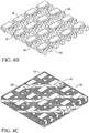
- FIG. 4A is a perspective view of multiple lead frames provided in a matrix.
- the lead frame is manufactured through mass production before the semiconductor dies are applied thereon.
- the lead frame units are connected with neighboring lead frame units.
- the connection between the lead frame units are rigid, so that the first and second parts are with predetermined assembly positions. Since the lead frame as shown in FIG. 3 includes dis-connected first and second parts, the rigid connection in FIG. 4A between each lead frame units can eliminate assembling the first and second parts in place before applying semiconductor dies thereon.
- the first part 342 of each lead frame unit 34 includes a first connection bar 354 at one side, the first connection bar 354 is used for connecting the first part 342 of the current lead frame unit 34 to the second part of a neighboring lead frame unit.
- second connection bars 356 are provided to connect the first part 342 of the current lead frame unit 34 to respectively the first part and the second part of a neighboring lead frame unit. More specifically, the first and second connection bars 354, 356 are provided on the first branch 346 of the first part 342.
- the first connection bar 354 connects the first branch 346 of the first part 342 of the current lead frame unit 34 and the first branch 350 of the second part of the neighboring lead frame unit.
- One of the second connection bars 356 connects the first branch 346 of the first part 342 of the current lead frame unit 34 and the second branch of the first part of another neighboring lead frame unit; while another second connection bar 356 connects the first branch 346 of the first part 342 of the current lead frame unit 34 and the second branch of the second part of the another neighboring lead frame unit.
- the one of the second connection 356 is connected to a sidewall of the second branch of the second part of the neighboring lead frame unit, which sidewall is the side of the protrusion of the second branch to be exposed after the encapsulation and singulation.
- FIG. 4B through FIG. 4E and FIGS. 5A - 5C are illustrative views of assemblies during packaging a semiconductor device according to exemplary embodiments.
- a semiconductor die and a corresponding lead frame are provided for packaging a semiconductor device. It will be described hereafter with reference to the semiconductor die as shown in FIG. 2A through FIG. 2C , and the lead frame as shown in FIG. 3 and FIG. 4A .
- the semiconductor die is attached to the lead frame through any suitable connection material, for example solder, glue, or adhesive.
- the connection material can be selected as conductive material, thereby providing electrical connection between the terminals of the device and the respective parts of the lead frame.
- the semiconductor die can be applied to the lead frame through various techniques, such as die bonding, etc . See FIG.
- the semiconductor die 32 is placed on the lead frame 34 with its first surface 322 facing the lead frame, and terminals 324, 326 connected to corresponding part of the lead frame respectively. After all semiconductor dies are placed, the assembly might be necessary to go through a reflow process, for soldering the semiconductor dies and the lead frame.
- the assembly of the semiconductor dies and the lead frame is molded using various applicable molding compounds, e.g. epoxy.
- the molded assembly is shown in FIG. 4C .
- the molding compound may cover the assembly while leaving the second surface 330 and the third terminal 332 of the semiconductor die 32, and the distal ends of the protrusion of the second branches 348, 352 exposed. As described previously, the second surface 330 and the distal ends of the protrusion of the second branches 348, 352 are co-planar.
- the molded assembly is grinded in the back in order to minimize the overall thickness of the final semiconductor device.
- the molding compound may cover the whole assembly, leaving only the second surface 330 and the distal ends of the protrusions exposed. It is thereby possible to remove the molding compound that covers the back of the assembly, i.e. at its side of the lead frame. It can be seen from FIG. 4E and FIG. 4C that, after grinding, a back side of the lead frame which is opposite to the side that the second branches 348, 352 are protruded is exposed. The grinding of the back side can allow the package size to be more compact because the thickness of the obtained semiconductor device is reduced.
- the lead frame is exposed both from the front side at the protrusions and from the back side at the bases of the first part and the second part, the heat generated by the semiconductor die, especially when operating under power pulses where transient voltages where heat generation is ultra-high, can be more efficiently conducted and dissipated.
- FIG. 5A is a perspective view of an obtained semiconductor device after singulation, from another aspect apart from that of FIG. 1 .
- FIG. 5B is a bottom view of the semiconductor device, seeing from the bottom surface 304 of the semiconductor device 30.
- the connection bars 354 and 356 are cut away during singulation, leaving sections thereof exposed on the sidewalls of the semiconductor device 30.
- the back surface of the base of the lead frame 34 is exposed.
- the exposed lead frame will function as additional heat sink for the semiconductor device 30.
- FIG. 5C is a perspective view of an obtained semiconductor device after grinding and singulation.
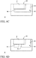
- FIG. 6A illustrates the cross-sectional views of the semiconductor device 30 along the sectional lines as in FIG. 1 .
- second branches 348, 352 are shown.
- FIG. 6B cross-sections of the first branches 346, 350, and the semiconductor die 32 are illustrated.
- FIG. 6C illustrates the cross-sectional view of the first part 342 of the lead frame 34, and the semiconductor die 32 placing on the lead frame 34, with first branch 346 and second branch 348 of the first part 342 being depicted as well.
- FIG. 6D shows the cross-sectional view of the first and second branches 350, 352 of the second part 344, the semiconductor die 32, and the first branch 346 of the first part 342.
- the semiconductor device and the lead frame allow the semiconductor die to have multiple contacts to be connected, while maintaining a more compact structure with constrained package size and thickness.
- the terminals at the active region side of the semiconductor die are connected through the lead frame to be co-planar with the terminal at the passive region side, which enables a no-lead package.
- the exposure of the protrusions on the sidewall of the semiconductor device further allows the semiconductor device to be side wettable during connection with external circuits like a PCB, which can improve the robustness of both mechanical and electrical connections.
Landscapes
- Engineering & Computer Science (AREA)
- Microelectronics & Electronic Packaging (AREA)
- Physics & Mathematics (AREA)
- Thermal Sciences (AREA)
- Lead Frames For Integrated Circuits (AREA)
- Structures Or Materials For Encapsulating Or Coating Semiconductor Devices Or Solid State Devices (AREA)
Abstract
Description
- The present invention is directed to semiconductor devices and lead frames for semiconductor devices, and more particularly to compact lead frame based semiconductor package.
Power devices, such as power MOSFETs, require high performance thermal capacity and heat dissipation because they are required to drain unwanted large currents to ground or other rails to protect devices connected thereto from being damaged. On the other hand, the power devices face challenges from structural compactness, which requires them to have a very small footprint and package height. - It is an object of the present invention to provide a lead frame based, compact, yet thermally efficient semiconductor package.
- This summary is provided to introduce a selection of concepts in a simplified form that are further described below in the Detailed Description. This summary is not intended to identify key features or essential features of the claimed subject matter, nor is it intended to be used to limit the scope of the claimed subject matter.
- In one embodiment, the present invention provides a semiconductor device, comprising a semiconductor die having a first side and an opposite second side, the semiconductor die comprising a first terminal on the first side and at least two second terminals on the second side, and a lead frame. The lead frame comprises first and second base parts that are mutually spaced from each other both electrically and mechanically, wherein the second side of the semiconductor die is mounted to the lead frame such that the at least two second terminals are electrically connected, respectively, to the first and second base parts. The lead frame further comprises first and second protrusions on the first and second base parts that project past a side of the die and provide first and second terminal surfaces that are co-planar with the first terminal on the first side of the semiconductor die.
- In another embodiment, the present invention provides a semiconductor device, comprising a semiconductor die having a first terminal on a first side and at least two second terminals on an opposite second side, and a lead frame having first and second parts. Each of the first and second parts comprises a base and a protrusion. The protrusions are respectively connected to and protrude from first sides of the bases. A height of the protrusions is substantially equal to a thickness of the semiconductor die, such that when the semiconductor die is mounted on the lead frame with the second side of the die facing the bases of the first and second parts of the lead frame, then the first side of the die is co-planar with distal ends of the protrusions.
- A semiconductor device, comprising: a semiconductor die comprising a first terminal on a first side and at least two second terminals on an opposite second side; and a lead frame comprising a first part and a second part, each of the first and second parts comprising a base and a protrusion, wherein the protrusions are respectively connected to and protrude from first sides of the bases, and wherein a height of the protrusions is substantially equal to a thickness of the semiconductor die, such that when the semiconductor die is mounted on the lead frame with the second side of the die facing the bases of the first and second parts of the lead frame, then the first side of the die is co-planar with distal ends of the protrusions.
- Each of the bases of the first part and second parts of the lead frame is connected to a corresponding one of the two second terminals of the semiconductor die. The distal ends of the protrusions and the first terminal are exposed on a bottom surface of the semiconductor device. Each of the bases of the first and second parts have second sides opposite to the first sides, wherein the second sides are exposed on a top surface of the semiconductor device. Sidewalls of the protrusions are exposed on a lateral sidewall of the semiconductor device. A molding compound may at least partially encapsulate the semiconductor die.
- The present invention further provides a lead frame for a semiconductor device. The lead frame comprises a first part including a first branch and a second branch, wherein the second branch is connected to and extends from the first branch. The lead frame also includes a second part having a third branch and a fourth branch, wherein the fourth branch is connected to and extends from the third branch. A first connection bar connects the first branch of the first part to the third branch of the second part of a neighboring lead frame when the lead frame is part of a matrix of lead frames. A second connection bar connects the first branch of the first part to the second and fourth branches respectively of the first and second parts of another neighboring lead frame. The second branch of the first part and the fourth branch of the second part extend in the same direction and to the same height.
- So that the manner in which the above recited features of the present invention can be understood in detail, a more particular description of the invention, briefly summarized above, may be had by reference to embodiments, some of which are illustrated in the appended drawings. It is to be noted, however, that the appended drawings illustrate only typical embodiments of this invention and are therefore not to be considered limiting of its scope, for the invention may admit to other equally effective embodiments. The drawings are for facilitating an understanding of the invention and thus are not necessarily drawn to scale. Advantages of the subject matter claimed will become apparent to those skilled in the art upon reading this description in conjunction with the accompanying drawings, in which like reference numerals have been used to designate like elements, and in which:
-
FIG. 1 is a perspective view of a semiconductor device in accordance with an embodiment of the present invention; -
FIG. 2A is a top plan view of a semiconductor die of the device ofFIG. 1 ; -
FIG. 2B is side view the semiconductor die ofFIG. 2A ; -
FIG. 2C is a bottom plan view of the semiconductor die ofFIG. 2A ; -
FIG. 3 is a perspective view of a lead frame of the semiconductor device ofFIG. 1 ; -
FIGS. 4A - 4E are perspective views illustrating steps for assembling the semiconductor device ofFIG. 1 ; -
FIG. 5A is a perspective view of an obtained semiconductor device after singulation; -
FIGS. 5B is a bottom plan view of the semiconductor device ofFIG. 5A , seeing from the bottom surface; -
FIG. 5C is a perspective view of an obtained semiconductor device after grinding and singulation; -
FIGS. 6A shows sectional lines on the semiconductor device ofFIG. 1 ; and -
FIGS. 6B - 6D are cross-sectional views of the semiconductor device along respective sectional lines ofFIG. 6A . -
FIG. 1 is a perspective view of asemiconductor device 30 in accordance with an embodiment. Thesemiconductor device 30 has atop surface 302 and anopposing bottom surface 304. On thebottom surface 304, thesemiconductor device 304 includesmultiple contacts contacts semiconductor device 30 to external circuit components, such as a printed circuit board (PCB). In the embodiment shown, thefirst contact 306 is exposed only on thebottom surface 304, while the second andthird contacts bottom surface 304 to alateral side wall 312 of thesemiconductor device 30 where they also are exposed. - The
first contact 306 is provided on a conductive surface of a semiconductor die of thesemiconductor device 30, while the second and thethird contacts first contact 306 is connected to a drain of the VDMOS, and the second andthird contacts semiconductor device 30 may be square or rectangular in shape, with a side length of 0.6mm, and a thickness of 0.4mm. In other embodiments, the semiconductor die can be provided as BJT, thyristor, etc. - Referring to
FIGS. 2A and 2B , a top plan view and a side view of asemiconductor die 32 of thesemiconductor device 30 are illustrated. The semiconductor die 32 is generally rectangular shaped. A major portion on afirst surface 322 is provided as afirst terminal 324, and the other portion on thefirst surface 322 is provided as asecond terminal 326. As discussed below, on an opposite second surface of the semiconductor die 32, a third terminal is provided. When packaged (seeFIG. 1 ), the first andsecond terminals contacts contact 306. The relative proportion of thefirst terminal 324 and thesecond terminal 326 is not limited to that illustrated inFIG. 2A . For example, in another embodiment, thesecond terminal 326 may have an area equal to or larger than that of thefirst terminal 324. To meet the size specification ofexample semiconductor device 30, discussed above, a length of the semiconductor die 32 is 0.5mm, and a width is 0.275mm. - In one embodiment,
studs 328 are disposed on thefirst surface 322. As illustrated inFIG. 2B , thestuds 328 are placed on top of thefirst surface 322, and with predetermined heights. In compliance with the device thickness as inFIG. 1 , the height of thestuds 328 can be 30µm, while the thickness of the semiconductor die 32 can be 145µm. A left bottom stud serves as the second terminal, while the other studs serve as the first terminal. In the example of a VDMOS, the left bottom stud can be connected to the gate of the VDMOS, while the other studs connected to the source of the VDMOS. It shall be the appreciation of any skilled person that, thestuds 328 can have any other suitable arrangements, and can be made of any suitable material, such as Cu. Furthermore, not all the studs are needed to be conductive. As mentioned above, on asecond surface 330 of the semiconductor die 32 opposite to thefirst surface 322, athird terminal 332 is provided, for example made of CuSn. As previously presented, in the example that the semiconductor die 32 is a VDMOS, thethird terminal 332 can be connected to the drain thereof. In other available embodiments, the semiconductor die can be provided as BJT, thyristor, etc.FIG. 3 is a perspective view of a unit of a lead frame matrix in accordance with an exemplary embodiment. Thelead frame 34 includes afirst part 342 and asecond part 344. Thefirst part 342 is distinguished and spaced apart from thesecond part 344. Each of thefirst part 342 and thesecond part 344 includes a first branch and a second branch. Thefirst branch 346 of thefirst part 342 is substantially flat. Thesecond branch 348 of thefirst part 342 is connected to an edge of thefirst branch 346, and extends from thefirst branch 346 to be substantially perpendicular to thefirst branch 346. Thefirst branch 350 of thesecond part 344 is co-planar with thefirst branch 346 of thefirst part 342. Thesecond branch 352 is connected to an edge of thefirst branch 350 in the same direction as that of the edge of thefirst branch 346 of thefirst part 342. Thesecond branch 352 extends from thefirst branch 350 to be substantially perpendicular to thefirst branch 350. Thesecond branches first branches second branch 352 of thesecond part 344 is aligned with thesecond branch 348 of thefirst part 342. Preferably, thesecond branches first branches - Each
part lead frame 34 is thereby provided to be including a base (first branch) and a protrusion (second branch) which connects to the base and protrudes from a first side of the base. The base of thefirst part 342 and thesecond base 344 are co-planar, collectively for receiving the semiconductor die 32 to be placed on the first side. A first side of the semiconductor die 32 is placed to face the first side of thefirst part 342 and thesecond part 344, while an opposite second side of the semiconductor die 32 is accordant to the ends of the protrusions. - In assembly, the
first part 342 and thesecond part 344 are respectively used for receiving and connecting to thefirst terminal 324 and thesecond terminal 326 of the semiconductor die 32. In which situation, the space between thefirst part 342 and thesecond part 344, as well as the sizes of thefirst part 342 and thesecond part 344, are adapted to be, in total, substantially similar to the size of the semiconductor die 32. Specifically, a width d from an edge of thefirst part 342 to an opposite edge of thesecond part 344 is generally equal to the width of the semiconductor die. - With reference to
FIG. 2A and FIG. 2B , in assembly, thefirst surface 322 of the semiconductor die 32 is placed facing thelead frame 34. Thestuds 328 of thefirst terminal 324 are connected to thefirst part 342, in particular, to thefirst branch 346 of thefirst part 342. Thestud 328 of thesecond terminal 326 is connected to thesecond part 344, in particular, to thefirst branch 350 of thesecond part 344. For providing a corresponding space for receiving thefirst terminal 324 and thesecond terminal 326, the proportion between thefirst branch 346 of thefirst part 342 and thefirst branch 350 of thesecond part 344 is approximated to that between thefirst terminal 324 and thesecond terminal 326 of the semiconductor die 32. Furthermore, the area of thefirst branch 346 of thefirst part 342 is at least as large as the area of thefirst terminal 324. Similarly, the area of thefirst branch 350 of thesecond part 344 is at least as large as the area of thesecond terminal 326. - It can hereby be understood that, the arrangement of the
first branches first terminal 324 and thesecond terminal 326. Since the connections to the first andsecond terminals second branches lead frame 34. The embodiment makes it possible to harmonize the compatibility between the package device and the PCB. For example, the PCB, especially the soldering pads for receiving and connecting to the package device, may not be necessarily modified in the situation that the first and second terminals of the semiconductor die are changed. - The extent that the
second branches first branches lead frame 34, thesecond surface 330 is generally co-planar with the distal ends of thesecond branches third terminal 332 is able to be in the same plane with electrical extensions of the first andsecond terminals lead frame 34 may be provided through known arts, like punching, etching, molding, etc. Each of thesecond branches branches lead frame 34 is made through etching, normally a piece of material is etched for obtainingfirst branches second branches first branches - After the semiconductor die 32 and the
lead frame 34 are encapsulated and singulated, thethird terminal 332 and the distal ends of the protrudingsecond branches FIG. 1 . Thethird terminal 332 is thereby provided as thefirst contact 306 of thesemiconductor device 30, thesecond branches second contacts second branches second branches second contacts bottom surface 304 of thesemiconductor device 30 to aside wall 312 thereof. - Referring still to
FIG. 3 , unlike the proportional arrangement of thefirst branches first terminal 324 and thesecond terminal 326, thesecond branches semiconductor device 30 to provide thesecond contact 308 and thethird contact 310. Thefirst terminal 324 and thesecond terminal 326 are electrically introduced along thefirst part 342 and thesecond part 344 of thelead frame 34, to be provided throughthird contact 310 and thesecond contact 308 for external links. The reliability of the electrical connection to the semiconductor die 32 can be enhanced. - According to an exemplary embodiment, active regions of the semiconductor die 32 are located on the side of the
first surface 322, the direct contact between thefirst surface 322 and thelead frame 34 will be advantageous for effectively dissipating heat generated by the active regions in a quickly and complete manner. This is especially useful for applications in which power peaks are needed to be dissipated. For this the heat capacity as build by the lead frame is of advantage. - Generally, the semiconductor die 32 generates heat during operation, which will increase the temperature within the semiconductor die 32. Considering necessary connections that dissipates the generated heat, the temperature within the die is determined by the heat resistance of the total set-up, including the package and the connected PCB. Transient pulse length is in such a range that the heat diffuses a few hundred microns. Such short pulses like ESD produce only local heating near the active junctions. In ESD applications, cooling with dissipating materials outside the package has limited effect.
- The semiconductor die 32 can be placed such that the active part of the die is finally soldered to a board. However, the cooling depends heavily on the board layout and board properties - parameter that depend on technology choices. Consequently, the actual robustness of the die cannot be predicted.
- According to an exemplary embodiment, the semiconductor die 32 is placed with the active side towards the lead frame. The cooling and the robustness are comparably better and more predictable. The robustness of the die in the application becomes independent (or at least less dependent) from the board layout and board properties. In such configuration the active side is adjacent to adequate heat dissipation material, allowing as low as possible heat resistance between the active side and the lead frame.
- It shall also be mentioned that,
FIG. 3 illustrates an exemplary embodiment of the unit of the lead frame with first andsecond parts FIG. 3 , and allows the active region of the semiconductor die to be placed facing the first branch. -
FIG. 4A is a perspective view of multiple lead frames provided in a matrix. As known, the lead frame is manufactured through mass production before the semiconductor dies are applied thereon. In the matrix shown inFIG. 4A , the lead frame units are connected with neighboring lead frame units. The connection between the lead frame units are rigid, so that the first and second parts are with predetermined assembly positions. Since the lead frame as shown inFIG. 3 includes dis-connected first and second parts, the rigid connection inFIG. 4A between each lead frame units can eliminate assembling the first and second parts in place before applying semiconductor dies thereon. - With reference to
FIG. 3 , thefirst part 342 of eachlead frame unit 34 includes afirst connection bar 354 at one side, thefirst connection bar 354 is used for connecting thefirst part 342 of the currentlead frame unit 34 to the second part of a neighboring lead frame unit. At another side of thefirst part 342, second connection bars 356 are provided to connect thefirst part 342 of the currentlead frame unit 34 to respectively the first part and the second part of a neighboring lead frame unit. More specifically, the first and second connection bars 354, 356 are provided on thefirst branch 346 of thefirst part 342. Thefirst connection bar 354 connects thefirst branch 346 of thefirst part 342 of the currentlead frame unit 34 and thefirst branch 350 of the second part of the neighboring lead frame unit. One of the second connection bars 356 connects thefirst branch 346 of thefirst part 342 of the currentlead frame unit 34 and the second branch of the first part of another neighboring lead frame unit; while anothersecond connection bar 356 connects thefirst branch 346 of thefirst part 342 of the currentlead frame unit 34 and the second branch of the second part of the another neighboring lead frame unit. The one of thesecond connection 356 is connected to a sidewall of the second branch of the second part of the neighboring lead frame unit, which sidewall is the side of the protrusion of the second branch to be exposed after the encapsulation and singulation. -
FIG. 4B through FIG. 4E andFIGS. 5A - 5C are illustrative views of assemblies during packaging a semiconductor device according to exemplary embodiments. For packaging a semiconductor device, a semiconductor die and a corresponding lead frame are provided. It will be described hereafter with reference to the semiconductor die as shown inFIG. 2A through FIG. 2C , and the lead frame as shown inFIG. 3 and FIG. 4A . The semiconductor die is attached to the lead frame through any suitable connection material, for example solder, glue, or adhesive. In particular applications, the connection material can be selected as conductive material, thereby providing electrical connection between the terminals of the device and the respective parts of the lead frame. The semiconductor die can be applied to the lead frame through various techniques, such as die bonding, etc. SeeFIG. 4B and with reference toFIG. 2A~2C andFIG. 3 , the semiconductor die 32 is placed on thelead frame 34 with itsfirst surface 322 facing the lead frame, andterminals - The assembly of the semiconductor dies and the lead frame is molded using various applicable molding compounds, e.g. epoxy. The molded assembly is shown in
FIG. 4C . The molding compound may cover the assembly while leaving thesecond surface 330 and thethird terminal 332 of the semiconductor die 32, and the distal ends of the protrusion of thesecond branches second surface 330 and the distal ends of the protrusion of thesecond branches - Referring to
FIG. 4D and FIG. 4E , according to an optional embodiment, the molded assembly is grinded in the back in order to minimize the overall thickness of the final semiconductor device. - As described above, the molding compound may cover the whole assembly, leaving only the
second surface 330 and the distal ends of the protrusions exposed. It is thereby possible to remove the molding compound that covers the back of the assembly, i.e. at its side of the lead frame. It can be seen fromFIG. 4E andFIG. 4C that, after grinding, a back side of the lead frame which is opposite to the side that thesecond branches - Singulation is followed to cut the molded (and optionally back-grinded) assembly into separate semiconductor device packages. Referring to
FIG. 1 , and with reference toFIG. 4D and FIG. 4E , singulation is carried along the sidewall of the second branches facing the neighboring lead frame, and along the lane between neighboring lead frames where first connection bars 354 are located. During singulation, the molding compound between neighboring lead frames are removed, and connection bars 354, 356 are cut and removed.FIG. 5A is a perspective view of an obtained semiconductor device after singulation, from another aspect apart from that ofFIG. 1 . -
FIG. 5B is a bottom view of the semiconductor device, seeing from thebottom surface 304 of thesemiconductor device 30. The connection bars 354 and 356 are cut away during singulation, leaving sections thereof exposed on the sidewalls of thesemiconductor device 30. On thetop surface 302 of thesemiconductor device 30, the back surface of the base of thelead frame 34 is exposed. In application, when thesemiconductor device 30 is mounted to an external circuit, e.g. a PCB, the exposed lead frame will function as additional heat sink for thesemiconductor device 30.FIG. 5C is a perspective view of an obtained semiconductor device after grinding and singulation. - Cross-sectional views of the
semiconductor device 30 along the sectional lines as inFIG. 1 are described below with reference toFIG. 6A - 6D . SeeFIG. 6A ,second branches FIG. 6B , cross-sections of thefirst branches FIG. 6C illustrates the cross-sectional view of thefirst part 342 of thelead frame 34, and the semiconductor die 32 placing on thelead frame 34, withfirst branch 346 andsecond branch 348 of thefirst part 342 being depicted as well.FIG. 6D shows the cross-sectional view of the first andsecond branches second part 344, the semiconductor die 32, and thefirst branch 346 of thefirst part 342. - The semiconductor device and the lead frame allow the semiconductor die to have multiple contacts to be connected, while maintaining a more compact structure with constrained package size and thickness. The terminals at the active region side of the semiconductor die are connected through the lead frame to be co-planar with the terminal at the passive region side, which enables a no-lead package. The exposure of the protrusions on the sidewall of the semiconductor device further allows the semiconductor device to be side wettable during connection with external circuits like a PCB, which can improve the robustness of both mechanical and electrical connections.
- The use of the terms "a" and "an" and "the" and similar referents in the context of describing the subject matter (particularly in the context of the following claims) are to be construed to cover both the singular and the plural, unless otherwise indicated herein or clearly contradicted by context. Recitation of ranges of values herein are merely intended to serve as a shorthand method of referring individually to each separate value falling within the range, unless otherwise indicated herein, and each separate value is incorporated into the specification as if it were individually recited herein. Furthermore, the foregoing description is for the purpose of illustration only, and not for the purpose of limitation, as the scope of protection sought is defined by the claims as set forth hereinafter together with any equivalents thereof entitled to. The use of any and all examples, or exemplary language (e.g., "such as") provided herein, is intended merely to better illustrate the subject matter and does not pose a limitation on the scope of the subject matter unless otherwise claimed. The use of the term "based on" and other like phrases indicating a condition for bringing about a result, both in the claims and in the written description, is not intended to foreclose any other conditions that bring about that result. No language in the specification should be construed as indicating any non-claimed element as essential to the practice of the invention as claimed.
- Preferred embodiments are described herein, including the best mode known to the inventor for carrying out the claimed subject matter. Of course, variations of those preferred embodiments will become apparent to those of ordinary skill in the art upon reading the foregoing description. The inventor expects skilled artisans to employ such variations as appropriate, and the inventor intends for the claimed subject matter to be practiced otherwise than as specifically described herein. Accordingly, this claimed subject matter includes all modifications and equivalents of the subject matter recited in the claims appended hereto as permitted by applicable law. Moreover, any combination of the above-described elements in all possible variations thereof is encompassed unless otherwise indicated herein or otherwise clearly contradicted by context.
Claims (13)
- A semiconductor device, comprising:a semiconductor die having a first side and an opposite second side, the semiconductor die comprising a first terminal on the first side and at least two second terminals on the second side; anda lead frame comprising:first and second base parts that are mutually spaced from each other both electrically and mechanically, wherein the second side of the semiconductor die is mounted to the lead frame such that the at least two second terminals are electrically connected, respectively, to the first and second base parts, andfirst and second protrusions on the first and second base parts that project past a side of the die and provide first and second terminal surfaces that are co-planar with the first terminal on the first side of the semiconductor die.
- The semiconductor device of claim 1, wherein areas of the at least two second terminals are different.
- The semiconductor device of any preceding claim, wherein each of the first and second base parts of the lead frame have an area corresponding to an area of the respectively connected second terminal.
- The semiconductor device of any preceding claim, wherein the semiconductor device has a top surface and a bottom surface, and the first side of the semiconductor die, and the first and second protrusions of the lead frame are exposed on the bottom surface.
- The semiconductor device of any preceding claim, wherein the first and second base parts of the lead frame respectively have exposed surfaces on the top surface of the semiconductor device.
- The semiconductor device of any preceding claim, wherein the first and second protrusions have exposed parts on a lateral side of the semiconductor device.
- The semiconductor device of any preceding claim, wherein the first and second protrusions extend perpendicularly from the first and second base parts.
- The semiconductor device of any preceding claim, wherein the semiconductor die comprises a VDMOS, a gate of the VDMOS is connected to a first one of the second terminals, a source of the VDMOS is connected to a second one of the second terminals, and a drain of the VDMOS is connected to the first terminal.
- The semiconductor device of any preceding claim, further comprising a molding compound that at least partially encapsulates the semiconductor die.
- A matrix of lead frames comprising multiple lead frame units arranged in a matrix, wherein each lead frame unit comprises:a first part comprising a first branch and a second branch, wherein the second branch is connected to and extends from the first branch;a second part comprising a third branch and a fourth branch, wherein the fourth branch is connected to and extends from the third branch;a first connection bar configured for connecting the first branch of the first part to the third branch of the second part of a neighboring lead frame unit; andsecond connection bars configured for connecting the first branch of the first part to the second and fourth branches respectively of the first and second parts of another neighboring lead frame unit,wherein the second branch of the first part and the fourth branch of the second part extend in the same direction and to the same height.
- The lead frame of claim 10, wherein the first and second connection bars are removable such that the first and second parts of each lead frame unit are electrically and mechanically separable.
- The lead frame of claims 10 to 11, wherein an area of the first branch of the first part is different from an area of the third branch of the second part.
- The lead frame of claims 10 to 12, wherein the each of the second and fourth branches protrudes perpendicularly from a side of the corresponding first and third branch.
Applications Claiming Priority (1)
| Application Number | Priority Date | Filing Date | Title |
|---|---|---|---|
| US15/180,072 US10256168B2 (en) | 2016-06-12 | 2016-06-12 | Semiconductor device and lead frame therefor |
Publications (1)
| Publication Number | Publication Date |
|---|---|
| EP3255667A1 true EP3255667A1 (en) | 2017-12-13 |
Family
ID=58489650
Family Applications (1)
| Application Number | Title | Priority Date | Filing Date |
|---|---|---|---|
| EP17165110.2A Pending EP3255667A1 (en) | 2016-06-12 | 2017-04-05 | Semiconductor device and lead frame therefor |
Country Status (3)
| Country | Link |
|---|---|
| US (1) | US10256168B2 (en) |
| EP (1) | EP3255667A1 (en) |
| CN (2) | CN107492535A (en) |
Cited By (1)
| Publication number | Priority date | Publication date | Assignee | Title |
|---|---|---|---|---|
| WO2021018566A1 (en) * | 2019-07-30 | 2021-02-04 | Osram Opto Semiconductors Gmbh | Lead frame assembly, method for producing a plurality of components, and component |
Families Citing this family (5)
| Publication number | Priority date | Publication date | Assignee | Title |
|---|---|---|---|---|
| IL285950B2 (en) | 2019-03-08 | 2025-07-01 | Siliconix Incorporated | Semiconductor package with coating on the side walls |
| US12224232B2 (en) | 2019-03-08 | 2025-02-11 | Siliconix Incorporated | Semiconductor package having side wall plating |
| CN110223966B (en) * | 2019-05-16 | 2021-05-07 | 宁波港波电子有限公司 | Lead frame and manufacturing method thereof |
| CN113035721A (en) | 2019-12-24 | 2021-06-25 | 维谢综合半导体有限责任公司 | Packaging process for plating conductive film on side wall |
| CN113035722A (en) | 2019-12-24 | 2021-06-25 | 维谢综合半导体有限责任公司 | Packaging process for plating with selective molding |
Citations (2)
| Publication number | Priority date | Publication date | Assignee | Title |
|---|---|---|---|---|
| US20040063240A1 (en) * | 2002-09-30 | 2004-04-01 | Fairchild Semiconductor Corporation | Semiconductor die package including drain clip |
| WO2009032537A1 (en) * | 2007-08-30 | 2009-03-12 | Fairchild Semiconductor Corporation | Semiconductor die package including stand off structures |
Family Cites Families (34)
| Publication number | Priority date | Publication date | Assignee | Title |
|---|---|---|---|---|
| US5814884C1 (en) | 1996-10-24 | 2002-01-29 | Int Rectifier Corp | Commonly housed diverse semiconductor die |
| US6133634A (en) | 1998-08-05 | 2000-10-17 | Fairchild Semiconductor Corporation | High performance flip chip package |
| US6262489B1 (en) | 1999-11-08 | 2001-07-17 | Delphi Technologies, Inc. | Flip chip with backside electrical contact and assembly and method therefor |
| JP3730469B2 (en) | 2000-01-21 | 2006-01-05 | 新電元工業株式会社 | Resin-sealed semiconductor device and manufacturing method thereof |
| CN1284421C (en) | 2000-03-22 | 2006-11-08 | 国际整流器公司 | Gate driver multi-chip module |
| US6624522B2 (en) | 2000-04-04 | 2003-09-23 | International Rectifier Corporation | Chip scale surface mounted device and process of manufacture |
| US6791172B2 (en) * | 2001-04-25 | 2004-09-14 | General Semiconductor Of Taiwan, Ltd. | Power semiconductor device manufactured using a chip-size package |
| US6646329B2 (en) * | 2001-05-15 | 2003-11-11 | Fairchild Semiconductor, Inc. | Power chip scale package |
| WO2003021664A1 (en) | 2001-08-31 | 2003-03-13 | Hitachi, Ltd. | Semiconductor device, structural body and electronic device |
| US6891256B2 (en) | 2001-10-22 | 2005-05-10 | Fairchild Semiconductor Corporation | Thin, thermally enhanced flip chip in a leaded molded package |
| US6946740B2 (en) | 2002-07-15 | 2005-09-20 | International Rectifier Corporation | High power MCM package |
| TWI232569B (en) | 2003-03-21 | 2005-05-11 | Comchip Technology Co Ltd | Metal bonding method for semiconductor circuit components employing prescribed feeds of metal balls |
| US6835580B1 (en) | 2003-06-26 | 2004-12-28 | Semiconductor Components Industries, L.L.C. | Direct chip attach structure and method |
| US7235877B2 (en) | 2004-09-23 | 2007-06-26 | International Rectifier Corporation | Redistributed solder pads using etched lead frame |
| JP4017625B2 (en) | 2004-09-30 | 2007-12-05 | 三洋電機株式会社 | Manufacturing method of semiconductor device |
| DE102005004160B4 (en) | 2005-01-28 | 2010-12-16 | Infineon Technologies Ag | CSP semiconductor device, semiconductor circuitry, and method of fabricating the CSP semiconductor device |
| US7504733B2 (en) * | 2005-08-17 | 2009-03-17 | Ciclon Semiconductor Device Corp. | Semiconductor die package |
| JP5141076B2 (en) | 2006-06-05 | 2013-02-13 | 株式会社デンソー | Semiconductor device |
| JP4503046B2 (en) | 2007-05-30 | 2010-07-14 | 株式会社東芝 | Manufacturing method of semiconductor device |
| US20090194856A1 (en) | 2008-02-06 | 2009-08-06 | Gomez Jocel P | Molded package assembly |
| US7767495B2 (en) * | 2008-08-25 | 2010-08-03 | Infineon Technologies Ag | Method for the fabrication of semiconductor devices including attaching chips to each other with a dielectric material |
| US7944031B2 (en) | 2008-11-24 | 2011-05-17 | Fairchild Semiconductor Corporation | Leadframe-based chip scale semiconductor packages |
| US8124449B2 (en) | 2008-12-02 | 2012-02-28 | Infineon Technologies Ag | Device including a semiconductor chip and metal foils |
| US8563360B2 (en) | 2009-06-08 | 2013-10-22 | Alpha And Omega Semiconductor, Inc. | Power semiconductor device package and fabrication method |
| US7939370B1 (en) | 2009-10-29 | 2011-05-10 | Alpha And Omega Semiconductor Incorporated | Power semiconductor package |
| US8513784B2 (en) * | 2010-03-18 | 2013-08-20 | Alpha & Omega Semiconductor Incorporated | Multi-layer lead frame package and method of fabrication |
| US8163601B2 (en) * | 2010-05-24 | 2012-04-24 | Alpha & Omega Semiconductor, Inc. | Chip-exposed semiconductor device and its packaging method |
| EP2421032A1 (en) | 2010-08-18 | 2012-02-22 | Nxp B.V. | Semiconductor Device Packaging Method and Semiconductor Device Package |
| EP2453476A1 (en) | 2010-11-12 | 2012-05-16 | Nxp B.V. | Semiconductor device packaging method and semiconductor device package |
| US8531016B2 (en) | 2011-05-19 | 2013-09-10 | International Rectifier Corporation | Thermally enhanced semiconductor package with exposed parallel conductive clip |
| US8436429B2 (en) * | 2011-05-29 | 2013-05-07 | Alpha & Omega Semiconductor, Inc. | Stacked power semiconductor device using dual lead frame and manufacturing method |
| EP2669936B1 (en) | 2012-06-01 | 2018-02-14 | Nexperia B.V. | Discrete semiconductor device package and manufacturing method |
| US9536800B2 (en) * | 2013-12-07 | 2017-01-03 | Fairchild Semiconductor Corporation | Packaged semiconductor devices and methods of manufacturing |
| US9117809B1 (en) * | 2014-03-09 | 2015-08-25 | Alpha & Omega Semiconductor (Cayman), Ltd. | Ultra-thin semiconductor device and preparation method thereof |
-
2016
- 2016-06-12 US US15/180,072 patent/US10256168B2/en active Active
-
2017
- 2017-04-05 EP EP17165110.2A patent/EP3255667A1/en active Pending
- 2017-06-12 CN CN201710439584.6A patent/CN107492535A/en active Pending
- 2017-06-12 CN CN202311391223.0A patent/CN117542821A/en active Pending
Patent Citations (2)
| Publication number | Priority date | Publication date | Assignee | Title |
|---|---|---|---|---|
| US20040063240A1 (en) * | 2002-09-30 | 2004-04-01 | Fairchild Semiconductor Corporation | Semiconductor die package including drain clip |
| WO2009032537A1 (en) * | 2007-08-30 | 2009-03-12 | Fairchild Semiconductor Corporation | Semiconductor die package including stand off structures |
Cited By (3)
| Publication number | Priority date | Publication date | Assignee | Title |
|---|---|---|---|---|
| WO2021018566A1 (en) * | 2019-07-30 | 2021-02-04 | Osram Opto Semiconductors Gmbh | Lead frame assembly, method for producing a plurality of components, and component |
| CN114270505A (en) * | 2019-07-30 | 2022-04-01 | 欧司朗光电半导体有限公司 | Lead frame composite, method for producing a plurality of components and component |
| US12125773B2 (en) | 2019-07-30 | 2024-10-22 | Osram Opto Semiconductors Gmbh | Lead frame assembly, method for producing a plurality of components, and component |
Also Published As
| Publication number | Publication date |
|---|---|
| CN107492535A (en) | 2017-12-19 |
| CN117542821A (en) | 2024-02-09 |
| US20170358514A1 (en) | 2017-12-14 |
| US10256168B2 (en) | 2019-04-09 |
Similar Documents
| Publication | Publication Date | Title |
|---|---|---|
| US10256168B2 (en) | Semiconductor device and lead frame therefor | |
| TWI450373B (en) | Double-sided cooling integrated power device package and module, and manufacturing method | |
| CN100362656C (en) | Semiconductor die package including drain clip and method of manufacturing the same | |
| US9029194B2 (en) | Making an integrated circuit module with dual leadframes | |
| US11088055B2 (en) | Package with dies mounted on opposing surfaces of a leadframe | |
| CN104218007B (en) | Small footprint semiconductor packages | |
| KR20080073735A (en) | Top and bottom exposed package semiconductor assembly device and method | |
| KR20100061700A (en) | Thermally enhanced thin semiconductor package | |
| EP3474322B1 (en) | Semiconductor device and method of manufacture | |
| KR101706825B1 (en) | Semiconductor package | |
| CN110634812B (en) | Semiconductor device package with clip interconnect and double-side cooling | |
| CN105304506A (en) | Exposed-Heatsink quad flat no-leads (QFN) package | |
| JP4899481B2 (en) | Manufacturing method of resin-encapsulated semiconductor device having a heat radiator exposed outside | |
| US9355946B2 (en) | Converter having partially thinned leadframe with stacked chips and interposer, free of wires and clips | |
| EP0086724A2 (en) | Integrated circuit lead frame with improved power dissipation | |
| CN212625552U (en) | Semiconductor chip packaging structure and electronic equipment | |
| US9449901B1 (en) | Lead frame with deflecting tie bar for IC package | |
| US12159818B2 (en) | Multi-chip packaged semiconductor device | |
| CN117012743A (en) | electronic components |
Legal Events
| Date | Code | Title | Description |
|---|---|---|---|
| PUAI | Public reference made under article 153(3) epc to a published international application that has entered the european phase |
Free format text: ORIGINAL CODE: 0009012 |
|
| STAA | Information on the status of an ep patent application or granted ep patent |
Free format text: STATUS: THE APPLICATION HAS BEEN PUBLISHED |
|
| AK | Designated contracting states |
Kind code of ref document: A1 Designated state(s): AL AT BE BG CH CY CZ DE DK EE ES FI FR GB GR HR HU IE IS IT LI LT LU LV MC MK MT NL NO PL PT RO RS SE SI SK SM TR |
|
| AX | Request for extension of the european patent |
Extension state: BA ME |
|
| STAA | Information on the status of an ep patent application or granted ep patent |
Free format text: STATUS: REQUEST FOR EXAMINATION WAS MADE |
|
| RBV | Designated contracting states (corrected) |
Designated state(s): AL AT BE BG CH CY CZ DE DK EE ES FI FR GB GR HR HU IE IS IT LI LT LU LV MC MK MT NL NO PL PT RO RS SE SI SK SM TR |
|
| 17P | Request for examination filed |
Effective date: 20180608 |
|
| STAA | Information on the status of an ep patent application or granted ep patent |
Free format text: STATUS: EXAMINATION IS IN PROGRESS |
|
| 17Q | First examination report despatched |
Effective date: 20201209 |