EP3255659A1 - Bonding method and bonded body - Google Patents
Bonding method and bonded body Download PDFInfo
- Publication number
- EP3255659A1 EP3255659A1 EP16761657.2A EP16761657A EP3255659A1 EP 3255659 A1 EP3255659 A1 EP 3255659A1 EP 16761657 A EP16761657 A EP 16761657A EP 3255659 A1 EP3255659 A1 EP 3255659A1
- Authority
- EP
- European Patent Office
- Prior art keywords
- wire bonding
- bump
- substrate
- chip
- bonding bump
- Prior art date
- Legal status (The legal status is an assumption and is not a legal conclusion. Google has not performed a legal analysis and makes no representation as to the accuracy of the status listed.)
- Withdrawn
Links
Images







Classifications
-
- B—PERFORMING OPERATIONS; TRANSPORTING
- B23—MACHINE TOOLS; METAL-WORKING NOT OTHERWISE PROVIDED FOR
- B23K—SOLDERING OR UNSOLDERING; WELDING; CLADDING OR PLATING BY SOLDERING OR WELDING; CUTTING BY APPLYING HEAT LOCALLY, e.g. FLAME CUTTING; WORKING BY LASER BEAM
- B23K20/00—Non-electric welding by applying impact or other pressure, with or without the application of heat, e.g. cladding or plating
- B23K20/002—Non-electric welding by applying impact or other pressure, with or without the application of heat, e.g. cladding or plating specially adapted for particular articles or work
- B23K20/004—Wire welding
-
- B—PERFORMING OPERATIONS; TRANSPORTING
- B23—MACHINE TOOLS; METAL-WORKING NOT OTHERWISE PROVIDED FOR
- B23K—SOLDERING OR UNSOLDERING; WELDING; CLADDING OR PLATING BY SOLDERING OR WELDING; CUTTING BY APPLYING HEAT LOCALLY, e.g. FLAME CUTTING; WORKING BY LASER BEAM
- B23K20/00—Non-electric welding by applying impact or other pressure, with or without the application of heat, e.g. cladding or plating
-
- H—ELECTRICITY
- H10—SEMICONDUCTOR DEVICES; ELECTRIC SOLID-STATE DEVICES NOT OTHERWISE PROVIDED FOR
- H10W—GENERIC PACKAGES, INTERCONNECTIONS, CONNECTORS OR OTHER CONSTRUCTIONAL DETAILS OF DEVICES COVERED BY CLASS H10
- H10W72/00—Interconnections or connectors in packages
- H10W72/01—Manufacture or treatment
- H10W72/011—Apparatus therefor
- H10W72/0112—Apparatus for manufacturing bump connectors
-
- H—ELECTRICITY
- H10—SEMICONDUCTOR DEVICES; ELECTRIC SOLID-STATE DEVICES NOT OTHERWISE PROVIDED FOR
- H10W—GENERIC PACKAGES, INTERCONNECTIONS, CONNECTORS OR OTHER CONSTRUCTIONAL DETAILS OF DEVICES COVERED BY CLASS H10
- H10W72/00—Interconnections or connectors in packages
- H10W72/01—Manufacture or treatment
- H10W72/011—Apparatus therefor
- H10W72/0115—Apparatus for manufacturing bond wires
-
- H—ELECTRICITY
- H10—SEMICONDUCTOR DEVICES; ELECTRIC SOLID-STATE DEVICES NOT OTHERWISE PROVIDED FOR
- H10W—GENERIC PACKAGES, INTERCONNECTIONS, CONNECTORS OR OTHER CONSTRUCTIONAL DETAILS OF DEVICES COVERED BY CLASS H10
- H10W72/00—Interconnections or connectors in packages
- H10W72/01—Manufacture or treatment
- H10W72/011—Apparatus therefor
- H10W72/0116—Apparatus for manufacturing strap connectors
-
- H—ELECTRICITY
- H10—SEMICONDUCTOR DEVICES; ELECTRIC SOLID-STATE DEVICES NOT OTHERWISE PROVIDED FOR
- H10W—GENERIC PACKAGES, INTERCONNECTIONS, CONNECTORS OR OTHER CONSTRUCTIONAL DETAILS OF DEVICES COVERED BY CLASS H10
- H10W72/00—Interconnections or connectors in packages
- H10W72/01—Manufacture or treatment
- H10W72/012—Manufacture or treatment of bump connectors, dummy bumps or thermal bumps
-
- H—ELECTRICITY
- H10—SEMICONDUCTOR DEVICES; ELECTRIC SOLID-STATE DEVICES NOT OTHERWISE PROVIDED FOR
- H10W—GENERIC PACKAGES, INTERCONNECTIONS, CONNECTORS OR OTHER CONSTRUCTIONAL DETAILS OF DEVICES COVERED BY CLASS H10
- H10W72/00—Interconnections or connectors in packages
- H10W72/01—Manufacture or treatment
- H10W72/012—Manufacture or treatment of bump connectors, dummy bumps or thermal bumps
- H10W72/01221—Manufacture or treatment of bump connectors, dummy bumps or thermal bumps using local deposition
- H10W72/01223—Manufacture or treatment of bump connectors, dummy bumps or thermal bumps using local deposition in liquid form, e.g. by dispensing droplets or by screen printing
-
- H—ELECTRICITY
- H10—SEMICONDUCTOR DEVICES; ELECTRIC SOLID-STATE DEVICES NOT OTHERWISE PROVIDED FOR
- H10W—GENERIC PACKAGES, INTERCONNECTIONS, CONNECTORS OR OTHER CONSTRUCTIONAL DETAILS OF DEVICES COVERED BY CLASS H10
- H10W72/00—Interconnections or connectors in packages
- H10W72/01—Manufacture or treatment
- H10W72/012—Manufacture or treatment of bump connectors, dummy bumps or thermal bumps
- H10W72/01221—Manufacture or treatment of bump connectors, dummy bumps or thermal bumps using local deposition
- H10W72/01225—Manufacture or treatment of bump connectors, dummy bumps or thermal bumps using local deposition in solid form, e.g. by using a powder or by stud bumping
-
- H—ELECTRICITY
- H10—SEMICONDUCTOR DEVICES; ELECTRIC SOLID-STATE DEVICES NOT OTHERWISE PROVIDED FOR
- H10W—GENERIC PACKAGES, INTERCONNECTIONS, CONNECTORS OR OTHER CONSTRUCTIONAL DETAILS OF DEVICES COVERED BY CLASS H10
- H10W72/00—Interconnections or connectors in packages
- H10W72/01—Manufacture or treatment
- H10W72/012—Manufacture or treatment of bump connectors, dummy bumps or thermal bumps
- H10W72/01251—Changing the shapes of bumps
-
- H—ELECTRICITY
- H10—SEMICONDUCTOR DEVICES; ELECTRIC SOLID-STATE DEVICES NOT OTHERWISE PROVIDED FOR
- H10W—GENERIC PACKAGES, INTERCONNECTIONS, CONNECTORS OR OTHER CONSTRUCTIONAL DETAILS OF DEVICES COVERED BY CLASS H10
- H10W72/00—Interconnections or connectors in packages
- H10W72/01—Manufacture or treatment
- H10W72/012—Manufacture or treatment of bump connectors, dummy bumps or thermal bumps
- H10W72/01251—Changing the shapes of bumps
- H10W72/01257—Changing the shapes of bumps by reflowing
-
- H—ELECTRICITY
- H10—SEMICONDUCTOR DEVICES; ELECTRIC SOLID-STATE DEVICES NOT OTHERWISE PROVIDED FOR
- H10W—GENERIC PACKAGES, INTERCONNECTIONS, CONNECTORS OR OTHER CONSTRUCTIONAL DETAILS OF DEVICES COVERED BY CLASS H10
- H10W72/00—Interconnections or connectors in packages
- H10W72/071—Connecting or disconnecting
- H10W72/0711—Apparatus therefor
- H10W72/07141—Means for applying energy, e.g. ovens or lasers
-
- H—ELECTRICITY
- H10—SEMICONDUCTOR DEVICES; ELECTRIC SOLID-STATE DEVICES NOT OTHERWISE PROVIDED FOR
- H10W—GENERIC PACKAGES, INTERCONNECTIONS, CONNECTORS OR OTHER CONSTRUCTIONAL DETAILS OF DEVICES COVERED BY CLASS H10
- H10W72/00—Interconnections or connectors in packages
- H10W72/071—Connecting or disconnecting
- H10W72/0711—Apparatus therefor
- H10W72/07178—Means for aligning
-
- H—ELECTRICITY
- H10—SEMICONDUCTOR DEVICES; ELECTRIC SOLID-STATE DEVICES NOT OTHERWISE PROVIDED FOR
- H10W—GENERIC PACKAGES, INTERCONNECTIONS, CONNECTORS OR OTHER CONSTRUCTIONAL DETAILS OF DEVICES COVERED BY CLASS H10
- H10W72/00—Interconnections or connectors in packages
- H10W72/071—Connecting or disconnecting
- H10W72/0711—Apparatus therefor
- H10W72/07183—Means for monitoring
-
- H—ELECTRICITY
- H10—SEMICONDUCTOR DEVICES; ELECTRIC SOLID-STATE DEVICES NOT OTHERWISE PROVIDED FOR
- H10W—GENERIC PACKAGES, INTERCONNECTIONS, CONNECTORS OR OTHER CONSTRUCTIONAL DETAILS OF DEVICES COVERED BY CLASS H10
- H10W72/00—Interconnections or connectors in packages
- H10W72/071—Connecting or disconnecting
- H10W72/072—Connecting or disconnecting of bump connectors
-
- H—ELECTRICITY
- H10—SEMICONDUCTOR DEVICES; ELECTRIC SOLID-STATE DEVICES NOT OTHERWISE PROVIDED FOR
- H10W—GENERIC PACKAGES, INTERCONNECTIONS, CONNECTORS OR OTHER CONSTRUCTIONAL DETAILS OF DEVICES COVERED BY CLASS H10
- H10W72/00—Interconnections or connectors in packages
- H10W72/071—Connecting or disconnecting
- H10W72/072—Connecting or disconnecting of bump connectors
- H10W72/07221—Aligning
- H10W72/07227—Aligning involving guiding structures, e.g. spacers or supporting members
-
- H—ELECTRICITY
- H10—SEMICONDUCTOR DEVICES; ELECTRIC SOLID-STATE DEVICES NOT OTHERWISE PROVIDED FOR
- H10W—GENERIC PACKAGES, INTERCONNECTIONS, CONNECTORS OR OTHER CONSTRUCTIONAL DETAILS OF DEVICES COVERED BY CLASS H10
- H10W72/00—Interconnections or connectors in packages
- H10W72/071—Connecting or disconnecting
- H10W72/072—Connecting or disconnecting of bump connectors
- H10W72/07231—Techniques
-
- H—ELECTRICITY
- H10—SEMICONDUCTOR DEVICES; ELECTRIC SOLID-STATE DEVICES NOT OTHERWISE PROVIDED FOR
- H10W—GENERIC PACKAGES, INTERCONNECTIONS, CONNECTORS OR OTHER CONSTRUCTIONAL DETAILS OF DEVICES COVERED BY CLASS H10
- H10W72/00—Interconnections or connectors in packages
- H10W72/071—Connecting or disconnecting
- H10W72/072—Connecting or disconnecting of bump connectors
- H10W72/07231—Techniques
- H10W72/07232—Compression bonding, e.g. thermocompression bonding
-
- H—ELECTRICITY
- H10—SEMICONDUCTOR DEVICES; ELECTRIC SOLID-STATE DEVICES NOT OTHERWISE PROVIDED FOR
- H10W—GENERIC PACKAGES, INTERCONNECTIONS, CONNECTORS OR OTHER CONSTRUCTIONAL DETAILS OF DEVICES COVERED BY CLASS H10
- H10W72/00—Interconnections or connectors in packages
- H10W72/071—Connecting or disconnecting
- H10W72/072—Connecting or disconnecting of bump connectors
- H10W72/07231—Techniques
- H10W72/07236—Soldering or alloying
-
- H—ELECTRICITY
- H10—SEMICONDUCTOR DEVICES; ELECTRIC SOLID-STATE DEVICES NOT OTHERWISE PROVIDED FOR
- H10W—GENERIC PACKAGES, INTERCONNECTIONS, CONNECTORS OR OTHER CONSTRUCTIONAL DETAILS OF DEVICES COVERED BY CLASS H10
- H10W72/00—Interconnections or connectors in packages
- H10W72/071—Connecting or disconnecting
- H10W72/072—Connecting or disconnecting of bump connectors
- H10W72/07251—Connecting or disconnecting of bump connectors characterised by changes in properties of the bump connectors during connecting
- H10W72/07253—Connecting or disconnecting of bump connectors characterised by changes in properties of the bump connectors during connecting changes in shapes
-
- H—ELECTRICITY
- H10—SEMICONDUCTOR DEVICES; ELECTRIC SOLID-STATE DEVICES NOT OTHERWISE PROVIDED FOR
- H10W—GENERIC PACKAGES, INTERCONNECTIONS, CONNECTORS OR OTHER CONSTRUCTIONAL DETAILS OF DEVICES COVERED BY CLASS H10
- H10W72/00—Interconnections or connectors in packages
- H10W72/20—Bump connectors, e.g. solder bumps or copper pillars; Dummy bumps; Thermal bumps
- H10W72/231—Shapes
- H10W72/234—Cross-sectional shape, i.e. in side view
-
- H—ELECTRICITY
- H10—SEMICONDUCTOR DEVICES; ELECTRIC SOLID-STATE DEVICES NOT OTHERWISE PROVIDED FOR
- H10W—GENERIC PACKAGES, INTERCONNECTIONS, CONNECTORS OR OTHER CONSTRUCTIONAL DETAILS OF DEVICES COVERED BY CLASS H10
- H10W72/00—Interconnections or connectors in packages
- H10W72/20—Bump connectors, e.g. solder bumps or copper pillars; Dummy bumps; Thermal bumps
- H10W72/241—Dispositions, e.g. layouts
-
- H—ELECTRICITY
- H10—SEMICONDUCTOR DEVICES; ELECTRIC SOLID-STATE DEVICES NOT OTHERWISE PROVIDED FOR
- H10W—GENERIC PACKAGES, INTERCONNECTIONS, CONNECTORS OR OTHER CONSTRUCTIONAL DETAILS OF DEVICES COVERED BY CLASS H10
- H10W72/00—Interconnections or connectors in packages
- H10W72/20—Bump connectors, e.g. solder bumps or copper pillars; Dummy bumps; Thermal bumps
- H10W72/241—Dispositions, e.g. layouts
- H10W72/242—Dispositions, e.g. layouts relative to the surface, e.g. recessed, protruding
-
- H—ELECTRICITY
- H10—SEMICONDUCTOR DEVICES; ELECTRIC SOLID-STATE DEVICES NOT OTHERWISE PROVIDED FOR
- H10W—GENERIC PACKAGES, INTERCONNECTIONS, CONNECTORS OR OTHER CONSTRUCTIONAL DETAILS OF DEVICES COVERED BY CLASS H10
- H10W72/00—Interconnections or connectors in packages
- H10W72/20—Bump connectors, e.g. solder bumps or copper pillars; Dummy bumps; Thermal bumps
- H10W72/241—Dispositions, e.g. layouts
- H10W72/247—Dispositions of multiple bumps
-
- H—ELECTRICITY
- H10—SEMICONDUCTOR DEVICES; ELECTRIC SOLID-STATE DEVICES NOT OTHERWISE PROVIDED FOR
- H10W—GENERIC PACKAGES, INTERCONNECTIONS, CONNECTORS OR OTHER CONSTRUCTIONAL DETAILS OF DEVICES COVERED BY CLASS H10
- H10W72/00—Interconnections or connectors in packages
- H10W72/20—Bump connectors, e.g. solder bumps or copper pillars; Dummy bumps; Thermal bumps
- H10W72/241—Dispositions, e.g. layouts
- H10W72/247—Dispositions of multiple bumps
- H10W72/248—Top-view layouts, e.g. mirror arrays
-
- H—ELECTRICITY
- H10—SEMICONDUCTOR DEVICES; ELECTRIC SOLID-STATE DEVICES NOT OTHERWISE PROVIDED FOR
- H10W—GENERIC PACKAGES, INTERCONNECTIONS, CONNECTORS OR OTHER CONSTRUCTIONAL DETAILS OF DEVICES COVERED BY CLASS H10
- H10W72/00—Interconnections or connectors in packages
- H10W72/20—Bump connectors, e.g. solder bumps or copper pillars; Dummy bumps; Thermal bumps
- H10W72/251—Materials
- H10W72/252—Materials comprising solid metals or solid metalloids, e.g. PbSn, Ag or Cu
-
- H—ELECTRICITY
- H10—SEMICONDUCTOR DEVICES; ELECTRIC SOLID-STATE DEVICES NOT OTHERWISE PROVIDED FOR
- H10W—GENERIC PACKAGES, INTERCONNECTIONS, CONNECTORS OR OTHER CONSTRUCTIONAL DETAILS OF DEVICES COVERED BY CLASS H10
- H10W72/00—Interconnections or connectors in packages
- H10W72/20—Bump connectors, e.g. solder bumps or copper pillars; Dummy bumps; Thermal bumps
- H10W72/29—Bond pads specially adapted therefor
-
- H—ELECTRICITY
- H10—SEMICONDUCTOR DEVICES; ELECTRIC SOLID-STATE DEVICES NOT OTHERWISE PROVIDED FOR
- H10W—GENERIC PACKAGES, INTERCONNECTIONS, CONNECTORS OR OTHER CONSTRUCTIONAL DETAILS OF DEVICES COVERED BY CLASS H10
- H10W72/00—Interconnections or connectors in packages
- H10W72/90—Bond pads, in general
- H10W72/941—Dispositions of bond pads
- H10W72/9415—Dispositions of bond pads relative to the surface, e.g. recessed, protruding
-
- H—ELECTRICITY
- H10—SEMICONDUCTOR DEVICES; ELECTRIC SOLID-STATE DEVICES NOT OTHERWISE PROVIDED FOR
- H10W—GENERIC PACKAGES, INTERCONNECTIONS, CONNECTORS OR OTHER CONSTRUCTIONAL DETAILS OF DEVICES COVERED BY CLASS H10
- H10W72/00—Interconnections or connectors in packages
- H10W72/90—Bond pads, in general
- H10W72/951—Materials of bond pads
- H10W72/952—Materials of bond pads comprising metals or metalloids, e.g. PbSn, Ag or Cu
-
- H—ELECTRICITY
- H10—SEMICONDUCTOR DEVICES; ELECTRIC SOLID-STATE DEVICES NOT OTHERWISE PROVIDED FOR
- H10W—GENERIC PACKAGES, INTERCONNECTIONS, CONNECTORS OR OTHER CONSTRUCTIONAL DETAILS OF DEVICES COVERED BY CLASS H10
- H10W90/00—Package configurations
- H10W90/701—Package configurations characterised by the relative positions of pads or connectors relative to package parts
- H10W90/721—Package configurations characterised by the relative positions of pads or connectors relative to package parts of bump connectors
- H10W90/724—Package configurations characterised by the relative positions of pads or connectors relative to package parts of bump connectors between a chip and a stacked insulating package substrate, interposer or RDL
Definitions
- the present invention relates to a bonding method and a bonded body.
- a chip loaded substrate is known in which a chip is loaded on a substrate.
- chip electrodes and substrate electrodes are bonded by various methods.
- a method is known in which the chip electrode and the substrate electrode are bonded through a bump formed on at least one of the chip electrode and the substrate electrode.
- Patent Literature 1 discloses that a film forming technique is used when a bump is to be formed on the electrode.
- the film forming technique is suitable for a mass production having an identical structure.
- the film forming technique does not sometimes suit to a small quantity production having a different structure.
- An object of the present invention is to provide a method of bonding a first member and a second member, in which a positional deviation between the first member and the second member can be reduced in case of bonding the first member and the second member through wire bonding bumps, and a bonded body in which a positional deviation between the first member and the second member can be reduced.
- a bonding method in some embodiments includes forming a first wire bonding bump (12) on a first electrode (14) arranged in a first member (10); forming a second wire bonding bump (22) on a second electrode (24) arranged in a second member (20); flattening a tip section (220) of the second wire bonding bump to form a bump flat surface (221); and pressure bonding a tip section (120) of the first wire bonding bump (12) and the bump flat surface (221) each other.
- a bonded body in some embodiments is a bonded body formed by the above bonding method.
- the present invention there are provided with the method of bonding the first member and the second member, in which a positional deviation between the first member and the second member can be reduced in case of bonding the first member and the second member through the wire bonding bump, and the bonded body in which a positional deviation between the first member and the second member can be reduced.
- a predetermined axis extending along a front surface of a first member (a surface to be bonded to a second member) or a back surface of the second member (a surface to be bonded to the first member) is defined as an X axis.
- An axis extending along the front surface of the first member or the back surface of the second member and perpendicular to the X axis is defined as a Y axis.
- An axis orthogonal to the X axis and the Y axis is defined as a Z axis.
- a "wire bonding bump” means a bump formed by wire bonding.
- a "first wire bonding bump” means a wire bonding bump formed on an electrode of a first member.
- a "second wire bonding bump” means a wire bonding bump formed on an electrode of a second member.
- a "first member” is, for example, a substrate or a chip.
- a "second member" is, for example, a substrate or a chip.
- the first member and the second member may be respectively a substrate and another substrate, a substrate and a chip, a chip and a substrate, or the chip and another chip.
- the first member may be a member except for the substrate and the chip.
- the second member may be a member except for the substrate and the chip.
- FIG. 1 is a perspective view schematically showing a substrate 10.
- FIG. 2 is a perspective view schematically showing a chip 20 to be loaded on the substrate.
- FIG. 3 is a sectional view schematically showing a part of a bonding process of the substrate 10 and the chip 20. Note that FIG. 1 to FIG. 3 are diagrams temporarily used to explain the matters recognized by the inventors. Therefore, FIG. 1 to FIG. 3 are not prior arts.
- the substrate 10 includes first wire bonding bumps 12 formed by the wire bonding technique.
- the chip 20 to be loaded on the substrate 10 includes second wire bonding bumps 22 formed by the wire bonding technique.
- a bump 12A, a bump 12B, a bump 12C, a bump 12D, a bump 12E, and a bump 12F on the substrate 10 are brought in contact with a bump 22A, a bump 22B, a bump 22C, a bump 22D, a bump 22E, a bump 22F on the chip 20, respectively.
- each of the wire bonding bumps (bump 12A and so on) of the substrate 10 has a tip section (tip section 120A and so on) protruding to an outward direction apart from the substrate 10.
- each wire bonding bump (bump 22A and so on) of the chip 20 includes a tip section (tip section 220A and so on) protruding to the outward direction apart from the chip 20.
- FIG. 3 shows the tip section 120A of the first wire bonding bump 12A, the tip section 120D of the first wire bonding bump 12D, the tip section 220A of the second wire bonding bump 22A, and the tip section 220D of the second wire bonding bump 22D.
- the tip section 120A of the first wire bonding bump 12A and the tip section 220A of the second wire bonding bump 22A are brought into contact with each other.
- force f is applied onto a contact surface 22a of the second wire bonding bump 22A.
- the chip 20 having the second wire bonding bump 22A is moved to a positive direction of the X axis by the X axial direction component Fx of the force f.
- the difference between the central axis 12c of the first wire bonding bump 12A and the central axis 22c of the second wire bonding bump 22A increases.
- the inventors recognized that the positional deviation between the substrate and the chip increases when connecting the substrate and the chip through the wire bonding bumps.
- the first member is the substrate 10 and the second member is the chip 20 will be described in the following description (using FIG. 4A to FIG. 4D ). Therefore, when the first member is a member except for the substrate, the “substrate” should be read as a "first member” in the following description. Also, when the second member is a member except for the chip, the "chip” should be read as a "second member” in the following description.
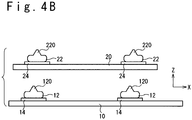
- FIG. 4A is a flow chart showing the bonding process of the substrate 10 and the chip 20. Also, FIG. 4B to FIG. 4D are sectional views schematically showing the bonding process of the substrate 10 and the chip 20.
- the first wire bonding bumps 12 are formed on first electrodes 14 (substrate electrodes) arranged on the substrate 10. Note that the number of electrodes 14 on the substrate 10 and the number of wire bonding bumps 12 formed on the electrodes 14 are optional.
- the first wire bonding bump 12 has the tip section 120 protruding in the outward direction apart from the substrate 10.
- the positions where the first wire bonding bumps 12 are formed are possible to set freely. For this reason, even if the substrates are of various kinds and of small quantity production, it is relatively easy to form the first wire bonding bump 12 on the electrode 14 of the substrate 10.
- the second wire bonding bumps 22 are formed on the second electrodes 24 (the chip electrode) arranged on the chip 20. Note that the number of electrodes 24 on the chip 20 and the number of wire bonding bumps 22 formed on the electrodes 24 are optional.
- the chip 20 after the second wire bonding bumps 22 are formed is shown.
- the second wire bonding bump 22 has the tip section 220 protruding in the outward direction apart from the chip 20.
- the positions where the second wire bonding bumps 22 are formed are possible to set freely. For this reason, even if the chips 20 are of various kinds and of small quantity production, it is relatively easy to form the second wire bonding bumps 22 on the electrodes 24 of the chip 20.
- step S2 may be executed before the first step S1.
- the tip section of the second wire bonding bump 22 is flattened.
- a bump flat surface 221 is formed in the second wire bonding bump 22 .
- the third step S3 is executed after the second step S2. Also, the third step S3 is executed before the first step S1 or after the first step S1.
- a fourth step S4 the tip section 120 of the first wire bonding bump 12 and the bump flat surface 221 are pressure bonded.
- the first wire bonding bump 12 and the second wire bonding bump 22 are pressure bonded to each other.
- the first wire bonding bump 12 and the second wire bonding bump 22 may be pressure bonded to each other.
- step S4 is executed after the first step S1 to the third step S3.
- FIG. 4A to FIG. 4D contains a step of flattening the tip sections of the second wire bonding bumps 22. Therefore, when the first wire bonding bumps 12 and the second wire bonding bumps 22 are pressure bonded to each other, the positional deviation of the central axis 12c of the first wire bonding bump 12 and the central axis 22c of the second wire bonding bump 22 does not increase.
- the positional deviation between the substrate and the chip can be reduced, compared with a case that the tip section of the bump is not flattened.
- the tip section of the first wire bonding bump (the tip section 120 in the example shown in FIG. 4D ) is not flattened before the first wire bonding bump 12 and the second wire bonding bump 22 are pressure bonded to each other. In other words, it is only the second wire bonding bump 22 that the flattening of the tip section is carried out at the third step S3.
- the first wire bonding bump 12 and the second wire bonding bump 22 are to be pressure bonded to each other, it is possible to increase a plane pressure acting on the bonding surface of the first wire bonding bump and the bonding surface of the second wire bonding bump (especially, at an initial step of the pressure bonding). As a result, the bonding strength between the first wire bonding bump and the second wire bonding bump increases. Or, the first wire bonding bump and the second wire bonding bump can be pressure bonded to each other in a smaller load.
- the substrate 10 and the chip 20 are pressure bonded through the first wire bonding bumps 12 on the substrate side and the second wire bonding bumps 22 on the chip side. Therefore, by using the first wire bonding bump 12 and the second wire bonding bump 22 having a comparatively thicker thickness as a buffering material or a cushion, it is restrained for the substrate 10, the substrate electrode 14, the chip 20 and the chip electrode 24 to be damaged by the pressure acting in the bonding.
- first member is the substrate 10 and the second member is the chip 20 will be described in the following description (the description with reference to FIG. 5 to FIG. 6N ). Therefore, when the first member is a member except for the substrate, the “substrate” should be read as the "first member” in the following description. Also, when the second member is a member except for the chip, the "chip” should be read as the "second member” in the following description.
- FIG. 5 is a flow chart to describe the bonding method of the substrate and the chip.
- the FIG. 6A and FIG. 6B are perspective views schematically showing the bonding process of the substrate 10 and the chip 20.
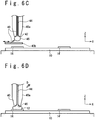
- FIG. 6C to FIG. 6N are sectional views schematically showing the bonding process of the substrate 10 and the chip 20. Note that in FIG. 5 to FIG. 6N , the same reference numeral is assigned to a member which has the same function as the member shown in FIG. 4A to FIG. 4D . Regarding the member having an identical reference numeral, the repetitive description is omitted.
- the substrate 10 having a plurality of substrate electrodes is prepared.
- the substrate electrode configures a part of a circuit formed in the substrate.
- the thickness of the substrate electrode is, for example, equal to or less than 1 ⁇ m.
- the material of the substrate electrode contains gold or aluminum.
- the material of the substrate 10 contains silicon (in other words, the substrate 10 is a silicon substrate).
- FIG. 6A shows the substrate 10 prepared at the first step S101.
- one electrode arranged on the substrate 10 is referred to as a first electrode 14 and another electrode arranged on the substrate 10 is referred to as a third electrode 14'.
- the chip 20 having a chip electrode is prepared.
- the chip electrode configures a part of a circuit formed in the chip.
- the thickness of the chip electrode is equal to or less than 1 ⁇ m.
- the material of the chip electrode contains gold or aluminum.
- the chip 20 is a semiconductor chip.
- the chip 20 is a memory, a CPU, a sensor, an analog circuit, MEMS or combinations of them.
- FIG. 6B shows the chip 20 prepared at the second step S102.
- one electrode arranged on the chip 20 is referred to as a second electrode 24, and another electrode arranged on the chip 20 is referred to a fourth electrode 24'.
- FIG. 6C to FIG. 6E are sectional views schematically showing the state in which the third step S103 is executed.
- a wire bonding apparatus 40 is shown.
- the wire bonding apparatus 40 is movable, for example, to an optional three-dimensional direction (a direction along the X axis, a direction along the Y axis and a direction along the Z axis).
- the wire bonding apparatus 40 includes a main unit section 40a and a discharge electrode 40b.
- the material 44 of a linear shape (wire-like shape) is accommodated in the main unit section 40a.
- the material 44 is accommodated in the main unit section 40a so as to be drawable from the opening formed in an end section 42 of the main unit section 40a.
- the material 44 is a material to form the wire bonding bump.
- the material 44 contains gold (Au).
- the discharge electrode 40b is an electrode to discharge for the material 44 drawn out from the opening formed in the end section 42.
- the discharge electrode 40b is electrically connected with a high-volt power supply (not illustrated).
- the discharge is caused based on a difference between the potential of the discharge electrode 40b and the potential of the material 44.
- the material 44 fuses due to the energy of the discharge.
- a spherical body 46 in the fusion state is formed in the tip of the material 44.
- the discharge electrode 40b may be configured to be relatively moveable to the main unit section 40a between an advanced position where the discharge electrode 40b faces the end section 42 of the main unit section 40a and a recessed position where it does not face the end section 42 of the main unit section 40a. After forming of the spherical body 46, the discharge electrode 40b is moved back to the recessed position.
- the wire bonding apparatus 40 moves to the first electrode 14 in the left part of the substrate 10.
- the wire bonding apparatus 40 moves to the direction along the Z axial direction.
- the spherical body 46 in the fusion state is brought in contact with the first electrode 14 in the left part of the substrate 10.
- FIG. 6D shows the state when the spherical body 46 has been brought in contact with the first electrode 14.
- the first wire bonding bump 12 (the spherical body 46 after change of the shape) is brought in contact with the first electrode 14, and the first wire bonding bump 12 is connected with the material 44 of the linear shape.
- the wire bonding apparatus 40 (the main unit section 40a) is moved from the state shown in FIG. 6D to a diagonally upward direction to the substrate 10 (for example, a direction shown by an arrow D).
- the wire bonding apparatus 40 moves to the outward direction apart from the substrate 10
- the wire bonding apparatus 40 moves to the direction along the surface of the substrate 10, (a direction along the surface of the substrate 10 and heading for the third electrode 14').
- FIG. 6E shows the state after the wire bonding apparatus 40 is moved diagonally upward to the substrate 10.
- the material 44 having the linear shape is cut by the movement of the wire bonding apparatus 40. Also, as the result of the cutting, the tip section 120 is formed in the first wire bonding bump 12 to protrude to the outward direction apart from the substrate 10.
- the tip section 120 is inclined to the direction to which the third electrode 14' is located (inclined to the direction shown by the arrow E from the direction perpendicular to the substrate 10).
- the step of forming the first wire bonding bump contains a step of cutting the material of the first wire bonding bump 12 so that the tip section 120 of the first wire bonding bump is inclined to the direction to which the third electrode 14' is located (it is because the step of forming the first wire bonding bump contains a step of cutting the material 44 of the wire bonding bump 12 by moving the wire bonding apparatus 40 to the direction shown by the arrow D to the substrate 10).
- the tip section 120 is inclined to the direction heading for the plane PL which passes a halfway point between the first electrode 14 and the third electrode 14' and which is perpendicular to a segment which links the first electrode 14 and the third electrode 14'.
- a plurality of wire bonding bumps are respectively formed on a plurality of electrodes (for example, all electrodes) arranged on the substrate 10.
- a third wire bonding bump is formed on the third electrode 14' arranged on the substrate 10.
- the step of forming the third wire bonding bump is similar to the step of forming the first wire bonding bump 12 until the step of pressure bonding the spherical body to the electrode. Therefore, only the step of cutting the third wire bonding bump will be described.
- FIG. 6F shows the state after the spherical body 46' (the spherical body after change of the shape) is brought in contact with the third electrode 14'.
- the third wire bonding bump 12' (the spherical body 46' after change of the shape) is brought in contact with the third electrode 14', and the third wire bonding bump 12' is in the state that it is connected with the material 44 having the linear shape.
- the wire bonding apparatus 40 (the main unit section 40a) is moved diagonally upward to the substrate 10 from the state shown in FIG. 6F (for example, a direction shown by the arrow G). In other words, when the wire bonding apparatus 40 is moved to the outward direction apart from the substrate 10, the wire bonding apparatus 40 is moved to the direction along the surface of the substrate 10, (the direction along the surface of the substrate 10 and heading for the first electrode 14).
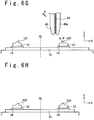
- FIG. 6G shows the state after the wire bonding apparatus 40 is moved diagonally upward to the substrate 10.
- the material 44 having the linear shape is cut by the movement of the wire bonding apparatus 40.
- the tip section 120' is formed in the third wire bonding bump 12' to protrude to the outward direction apart from the substrate 10.
- the tip section 120' is inclined to the direction to which the first electrode 14 is located (inclined to the direction shown by the arrow H from the direction perpendicular to the substrate 10).
- the step of forming the third wire bonding bump contains a step of cutting the material of the third wire bonding bump 12' so that the tip section 120' of the third wire bonding bump is inclined to the direction to which the first electrode 14 is located (this is because containing a step of cutting the material 44 of the wire bonding bump by moving the wire bonding apparatus 40 to the direction shown by the arrow G to the substrate 10).
- the tip section 120' is inclined to the direction heading for the plane PL which passes a halfway point between the first electrode 14 and the third electrode 14' and which is perpendicular to a segment linking the first electrode 14 and the third electrode 14'.
- the orientation of the tip section 120' of the third wire bonding bump 12' is different from the orientation of the tip section 120 of the first wire bonding bump 12 (for example, the direction of the central axis of the tip section 120). More specifically, the tip section 120' and the tip section 120 are inclined to face each other.
- the tip section 120' and the tip section 120 may be inclined the directions apart from each other. That is, the step of forming the first wire bonding bump may contain a step of cutting the material of the first wire bonding bump 12 so that the tip section 120 of the first wire bonding bump is inclined to a direction opposite to the direction to which the third electrode 14' is located, and the step of forming the third wire bonding bump may contain a step of cutting the material of the third wire bonding bump 12' so that the tip section 120' of the third wire bonding bump 12' is inclined to a direction opposite to the direction which the first electrode 14 is located.
- a plurality of wire bonding bumps of a desired number are respectively formed on a plurality of electrodes arranged on the substrate 10.
- a second wire bonding bump 22 is formed on the second electrode 24 of the chip 20.
- the fourth step S104 is a step to be executed after the second step S102.
- the step of forming the second wire bonding bump 22 on the second electrode 24 of the chip 20 is similar to the step of forming the first wire bonding bump 12 on the first electrode 14 of the substrate 10. Therefore, the repetitive description is omitted.
- FIG. 6H shows the state after the second wire bonding bump 22 is formed on the second electrode 24 of the chip 20 at the fourth step S104, and the fourth wire bonding bump 22' is formed on the fourth electrode 24'.
- the fourth step S104 the plurality of wire bonding bumps of the desired number are formed on the plurality of electrodes arranged on the chip 20, respectively.
- first step S101 and the third step S103 may be executed before the second step and the fourth step S104, or may be executed after the second step and the fourth step S104, or may be executed simultaneously with the second step and the fourth step S104, respectively.
- a fifth step S105 is executed.
- the fifth step S105 is a step of forming a bump flat surface.
- the tip section of the second wire bonding bump 22 is flattened.
- a bump flat surface is formed in the second wire bonding bump.
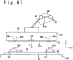
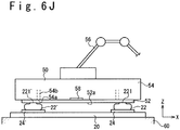
- a flat surface forming apparatus 50 is shown in FIG. 6I .
- the flat surface forming device 50 includes a pushing member 52 which pushes the tip section 220 of the second wire bonding bump 22, a pushing block 54 which holds the pushing member 52, and a pushing member moving mechanism 56 (or a pushing block moving mechanism).
- the flat surface forming apparatus 50 may include a pressure sensor 58.
- the pushing member 52 has a flat surface 52a which contacts the tip section 220 of the second wire bonding bump 22.
- the pushing member 52 is a board-like (specifically, tabular) member.
- the pushing member 52 is a silicon board (more specifically, a silicon flat board).
- the pushing member 52 is formed of the silicon material.
- the silicon board is a board in which an oxide film is a formed on the surface of the silicon material.
- the silicon board when a silicon board is used as the pushing member 52, the silicon board has the thickness of 0.05 mm to 1 mm.
- the pushing block 54 is a member which holds the pushing member 52.
- the pushing block 54 holds the pushing member 52 detachably.
- the pushing block 54 has an absorption hole 54a to absorb the pushing member 52 and a pipe route 54b communicating with the absorption hole 54a.
- the pipe route 54b is connected with a suction pump and so on (not illustrated).
- the pushing member moving mechanism 56 is a mechanism to move the pushing member 52 relatively to the chip 20 arranged on a stage 60.
- the pushing member moving mechanism 56 may have, for example, a driver (not illustrated), arm members 56a, and pivot sections 56b.
- the pushing member moving mechanism 56 may move the pushing member 52 (and the pushing block 54) only in the direction along the Z axis (in other words, the direction perpendicular to the chip back surface 26).
- the pushing member moving mechanism 56 may move the pushing member 52 (and the pushing block 54) to an optional direction in the three-dimensional space.
- the pushing member moving mechanism 56 moves the pushing member 52 for the tip section 220 of the second wire bonding bump.
- the pushing member 52 is moved so that the tip section 220 of the second wire bonding bump 22 is brought in contact with the flat surface 52a of the pushing member 52.
- the pushing member 52 is moved so that the tip section 220 of the second wire bonding bump 22 are flattened by the pushing member 52.
- the pushing member 52 is moved to a direction shown by the arrow I (in other words, the pushing member 52 is moved downwardly for the chip 20), to crush the tip section 220 of the second wire bonding bump 22 and to flatten the tip section 220 of the second wire bonding bump 22.
- the stage 60 to support the chip 20 may be lifted up for the pushing member 52 to crush the tip section 220 of the second wire bonding bump 22 and to flatten the tip section 220 of the second wire bonding bump 22.
- FIG. 6J show the state after the tip section 220 of the second wire bonding bump 22 is flattened. By the flattening, the bump flat surface 221 is formed in the second wire bonding bump. Note that in the example shown in FIG. 6I and FIG. 6J , the tip sections of all the wire bonding bumps on the electrodes arranged on the chip 20 are crushed at a same time (in other words, the bump flat surfaces (the bump flat surface 221, the bump flat surface 221' and so on) are formed at a same time to all the wire bonding bumps). Therefore, the time taken to form the bump flat surfaces is shortened.
- FIG. 6K is a schematic sectional view showing the bump flat surface 221 formed by the fifth step S105.
- the sectional view viewed from the direction of the F-F arrows is a sectional view, in which the area of the second wire bonding bump 22 is maximum, of sectional views parallel to the bump flat surface 221 of the second wire bonding bump 22.
- the area of the bump flat surface 221 is, for example, 30% or more and 90% or below of the area of the second wire bonding bump 22 viewed from the direction of the F-F arrow.
- the tip section 220 of the second wire bonding bump 22 is crushed so that the area of the bump flat surface 221 is equal to or more than 30% of the maximum cross section area of the second wire bonding bump 22 (the cross section area in the sectional view viewed from the direction of the F-F arrow). As a result, the situation that the area of the bump flat surface 221 becomes too little can be avoided. Also, the tip section 220 of the second wire bonding bump 22 is crushed so that the area of the bump flat surface 221 is less than 90% of the maximum cross section area of the second wire bonding bump 22 (the cross section area in the sectional view viewed from the direction of the F-F arrow). As the result, the situation that the proximal section 222 of the second wire bonding bump 22 (a part other than the tip section 220) is crushed too much can be avoided.
- a total area of the bump flat surfaces (a summation of areas of the bump flat surfaces) is correlated with, for example, the pressure which acts on the pushing block 54. Therefore, if the pressure which acts on the pushing block 54 is measured by the pressure sensor 58 arranged on (the surface of) the pushing block 54 and the pushing member moving mechanism 56 is controlled based on the measured pressure, it is possible to control the total area of the bump flat surfaces.
- the maximum cross section area of the second wire bonding bump 22 (the cross section area viewed from the direction of the F-F arrows) is, for example, equal to or more than 2.5 ⁇ 10 -11 ⁇ m 2 , and equal to or less than 1.0 ⁇ 010 -8 ⁇ m 2 .
- the area of the bump flat surface 221 is, for example, equal to or more than 7.5 ⁇ 10 -12 ⁇ m 2 , and equal to or less than 9.0 ⁇ 10 -9 ⁇ m 2 .
- a sixth step S106 is a heating step of heating the flattened wire bonding bump.
- the second wire bonding bump is heated such that the second wire bonding bump having the bump flat surface becomes hotter than the first wire bonding bump.
- the sixth step S106 will be described.
- the sixth step S106 is executed after execution of the fifth step S105 and before execution of the following seventh step S107.
- the stage 72 as a heater is shown in FIG. 6L .
- the stage 72 has the heater.
- the chip 20 is supported by the stage 72.
- the arranging of the heater is not limited to an example shown in FIG. 6L and is optional.
- the heater heats the flattened second wire bonding bump 22 to a temperature below the melting point of the bump.
- the heater heats the flattened second wire bonding bump 22 to, for example, a temperature of 100 °C or above and of 250 °C or below.
- the flattened second wire bonding bump 22 is softened through the heating.
- the sixth step may be incorporated into the fifth step.
- the fifth step the step of forming the bump flat surface
- the sixth step can be executed at the same time.
- the sixth step may be incorporated into the following seventh step. For example, if the heater is incorporated into the holding block to hold the chip 20, the seventh step and the sixth step can be executed at the same time.
- sixth step S106 may be omitted.
- the seventh step S107 is a pressure bonding step of pressure-bonding the first wire bonding bump and the second wire bonding bump.
- the seventh step is executed after the fifth step S105.
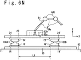
- FIG. 6M shows a pressure bonding apparatus 80.
- the pressure bonding apparatus 80 includes a holding block 82 and a holding block moving mechanism 84.
- the pressure bonding apparatus 80 may have a pressure sensor 86.
- the holding block 82 is a holding member for holding the chip 20.
- the holding block 82 has an absorption hole 82a to absorb the chip 20 and a pipe route 82b communicating with the absorption hole 82a.
- the pipe route 82b is connected with a suction pump and so on (not illustrated).
- the holding block 82 holds the chip 20 detachably by the vacuum absorption.
- the holding block moving mechanism 84 is a mechanism for moving the holding block 82 relatively to the substrate 10 arranged on the stage 92.
- the holding block moving mechanism 84 may include, for example, a driver (not illustrated), arm members 84a and pivot sections 84b.
- the holding block moving mechanism 84 may be able to move the holding block 82 only to the direction along the Z axis (in other words, the direction perpendicular to the front surface 16 of the substrate 10).
- the holding block moving mechanism 84 may be able to move the holding block 82 to an optional three-dimensional optional direction.
- the holding block moving mechanism 84 moves the holding block 82 toward the tip section 120 of the first wire bonding bump 12.
- the tip section 120 of the first wire bonding bump 12 is brought in contact with the bump flat surface 221 of the second wire bonding bump 22.
- the tip section 120 of the first wire bonding bump 12 sticks the bump flat surface 221 of the second wire bonding bump 22.
- the tip section 120 of first wire bonding bump 12 and the bump flat surface 221 of the second wire bonding bump are pressure bonded to each other.
- the tip section 120 of the first wire bonding bump 12 and the tip section 120' of the third wire bonding bump 12' are inclined to directions to face each other. Therefore, the relative movement of the substrate 10 and the chip 20, such as movement to the X direction, is constrained when the first wire bonding bump 12 and the second wire bonding bump 22 are pressure bonded and the third wire bonding bump 12' and the fourth wire bonding bump 22' are pressure bonded. As a result, the generation of the positional deviation is effectively restrained in case of bonding of the substrate 10 and the chip 20.
- the second wire bonding bump 22 having the bump flat surface 221 is softened at the sixth step (the heating step)
- a sticking quantity of the tip section 120 of the first wire bonding bump 12 to the bump flat surface 221 increases.
- the bonding strength between the wire bonding bumps increases.
- the second wire bonding bump 22 having the bump flat surface 221 is softened at the sixth step (the heating step)
- FIG. 6N shows the state after execution of the seventh step S107.
- the substrate 10 and the chip 20 are bonded through the first wire bonding bump 12 and the second wire bonding bump 22. Also, the substrate 10 and the chip 20 are bonded through the third wire bonding bump 12' and the fourth wire bonding bump 22'.
- the substrate 10 and the chip 20 forms one bonded body.
- the distance L1 between one bonded wire bonding bump 100A and another neighbor bonded wire bonding bump 100B is, for example, from 1 ⁇ m to 1000 ⁇ m, 10 ⁇ m to 1000 ⁇ m, 1 ⁇ m to 100 ⁇ m, or 10 ⁇ m to 100 ⁇ m.
- the examples shown in FIG. 5 to FIG. 6N provide the same advantageous effects as in the example shown in FIG. 4A to FIG. 4D . Also, in the examples shown in FIG. 5 to FIG. 6N , when the pushing member 52 is a silicon board, it is possible to improve the flatness of the bump flat surface which has been formed through the contact with the pushing member 52. In the examples shown in FIG. 5 to FIG. 6N , when the bonding method of the substrate and the bumps contains the step of heating the wire bonding bump having the bump flat surface, the first wire bonding bump and the second wire bonding bump can be bonded by using the relatively small pushing pressure.
Landscapes
- Engineering & Computer Science (AREA)
- Mechanical Engineering (AREA)
- Wire Bonding (AREA)
- Pressure Welding/Diffusion-Bonding (AREA)
- Manufacturing & Machinery (AREA)
Abstract
Description
- The present invention relates to a bonding method and a bonded body.
- A chip loaded substrate is known in which a chip is loaded on a substrate. When the chip loaded substrate is manufactured, chip electrodes and substrate electrodes are bonded by various methods. As the method of bonding the chip electrode and the substrate electrode, a method is known in which the chip electrode and the substrate electrode are bonded through a bump formed on at least one of the chip electrode and the substrate electrode.
- As the related technique, Patent Literature 1 discloses that a film forming technique is used when a bump is to be formed on the electrode. The film forming technique is suitable for a mass production having an identical structure. On the other hand, the film forming technique does not sometimes suit to a small quantity production having a different structure.
- [Patent Literature 1]
JP 2005-243714A - An object of the present invention is to provide a method of bonding a first member and a second member, in which a positional deviation between the first member and the second member can be reduced in case of bonding the first member and the second member through wire bonding bumps, and a bonded body in which a positional deviation between the first member and the second member can be reduced.
- A bonding method in some embodiments includes forming a first wire bonding bump (12) on a first electrode (14) arranged in a first member (10); forming a second wire bonding bump (22) on a second electrode (24) arranged in a second member (20); flattening a tip section (220) of the second wire bonding bump to form a bump flat surface (221); and pressure bonding a tip section (120) of the first wire bonding bump (12) and the bump flat surface (221) each other.
- A bonded body in some embodiments is a bonded body formed by the above bonding method.
- According to the present invention, there are provided with the method of bonding the first member and the second member, in which a positional deviation between the first member and the second member can be reduced in case of bonding the first member and the second member through the wire bonding bump, and the bonded body in which a positional deviation between the first member and the second member can be reduced.
- The attached drawings are incorporated into this Specification to help the description of embodiments. Note that the drawings should not be interpreted to limit the present invention to illustrated and described examples.
- [
FIG. 1] FIG. 1 is a perspective view schematically showing a substrate. - [
FIG. 2] FIG. 2 is a perspective view schematically showing a chip loaded on the substrate. - [
FIG. 3] FIG. 3 is a sectional view schematically showing a part of a bonding step of the substrate and the chip. - [
FIG. 4A] FIG. 4A is a flow chart showing the bonding process of the substrate and the chip. - [
FIG. 4B] FIG. 4B is a sectional view schematically showing the bonding process of the substrate and the chip. - [
FIG. 4C] FIG. 4C is a sectional view schematically showing the bonding process of the substrate and the chip. - [
FIG. 4D] FIG. 4D is a sectional view schematically showing the bonding process of the substrate and the chip. - [
FIG. 5] FIG. 5 is a flow chart which explains the bonding method of the substrate and the chip. - [
FIG. 6A] FIG. 6A is a perspective view schematically showing the bonding process of the substrate and the chip. - [
FIG. 6B] FIG. 6B is a perspective view schematically showing the bonding process of the substrate and the chip. - [
FIG. 6C] FIG. 6C is a sectional view schematically showing the bonding process of the substrate and the chip. - [
FIG. 6D] FIG. 6D is a sectional view schematically showing the bonding process of the substrate and the chip. - [
FIG. 6E] FIG. 6E is a sectional view schematically showing the bonding process of the substrate and the chip. - [
FIG. 6F] FIG. 6F is a sectional view schematically showing the bonding process of the substrate and the chip. - [
FIG. 6G] FIG. 6G is a sectional view schematically showing the bonding process of the substrate and the chip. - [
FIG. 6H] FIG. 6H is a sectional view schematically showing the bonding process of the substrate and the chip. - [
FIG. 6I] FIG. 6I is a sectional view schematically showing the bonding process of the substrate and the chip. - [
FIG. 6J] FIG. 6J is a sectional view schematically showing the bonding process of the substrate and the chip. - [
FIG. 6K] FIG. 6K is a sectional view schematically showing the bonding process of the substrate and the chip. - [
FIG. 6L] FIG. 6L is a sectional view schematically showing the bonding process of the substrate and the chip. - [
FIG. 6M] FIG. 6M is a sectional view schematically showing the bonding process of the substrate and the chip. - [
FIG. 6N] FIG. 6N is a sectional view schematically showing the bonding process of the substrate and the chip. - In the following detailed description, many detailed specific matters are disclosed for the purpose of the description to provide the comprehensive understanding of embodiments. However, it would be apparent that one or plural embodiments are executable without these detailed specific matters. Hereinafter, a bonding method and a bonded body will be described with reference to the attached drawings.
- A predetermined axis extending along a front surface of a first member (a surface to be bonded to a second member) or a back surface of the second member (a surface to be bonded to the first member) is defined as an X axis. An axis extending along the front surface of the first member or the back surface of the second member and perpendicular to the X axis is defined as a Y axis. An axis orthogonal to the X axis and the Y axis is defined as a Z axis.
- In this Specification, a "wire bonding bump" means a bump formed by wire bonding.
- In this Specification, a "first wire bonding bump" means a wire bonding bump formed on an electrode of a first member.
- In this Specification, a "second wire bonding bump" means a wire bonding bump formed on an electrode of a second member.
- In this Specification, a "first member" is, for example, a substrate or a chip.
- In this Specification, a "second member" is, for example, a substrate or a chip.
- In this Specification, the first member and the second member may be respectively a substrate and another substrate, a substrate and a chip, a chip and a substrate, or the chip and another chip.
- In this Specification, the first member may be a member except for the substrate and the chip. Also, the second member may be a member except for the substrate and the chip.
- Referring to
FIG. 1 to FIG. 3 , the matters recognized by the inventors will be described.FIG. 1 is a perspective view schematically showing asubstrate 10.FIG. 2 is a perspective view schematically showing achip 20 to be loaded on the substrate.FIG. 3 is a sectional view schematically showing a part of a bonding process of thesubstrate 10 and thechip 20. Note thatFIG. 1 to FIG. 3 are diagrams temporarily used to explain the matters recognized by the inventors. Therefore,FIG. 1 to FIG. 3 are not prior arts. - As shown in
FIG. 1 , thesubstrate 10 includes first wire bonding bumps 12 formed by the wire bonding technique. - As shown in
FIG. 2 , thechip 20 to be loaded on thesubstrate 10 includes second wire bonding bumps 22 formed by the wire bonding technique. - When the
substrate 10 andchip 20 are to be bonded, it is assumed that abump 12A, abump 12B, a bump 12C, abump 12D, abump 12E, and abump 12F on thesubstrate 10 are brought in contact with abump 22A, abump 22B, abump 22C, abump 22D, abump 22E, abump 22F on thechip 20, respectively. - As shown in
FIG. 3 , each of the wire bonding bumps (bump 12A and so on) of thesubstrate 10 has a tip section (tip section 120A and so on) protruding to an outward direction apart from thesubstrate 10. Also, each wire bonding bump (bump 22A and so on) of thechip 20 includes a tip section (tip section 220A and so on) protruding to the outward direction apart from thechip 20.FIG. 3 shows thetip section 120A of the firstwire bonding bump 12A, thetip section 120D of the firstwire bonding bump 12D, thetip section 220A of the secondwire bonding bump 22A, and thetip section 220D of the secondwire bonding bump 22D. - By applying force F onto the
chip 20, thetip section 120A of the firstwire bonding bump 12A and thetip section 220A of the secondwire bonding bump 22A are brought into contact with each other. As the reaction to the force which acts on acontact surface 12a of the firstwire bonding bump 12A, force f is applied onto acontact surface 22a of the secondwire bonding bump 22A. Thechip 20 having the secondwire bonding bump 22A is moved to a positive direction of the X axis by the X axial direction component Fx of the force f. As a result, the difference between thecentral axis 12c of the firstwire bonding bump 12A and the central axis 22c of the secondwire bonding bump 22A increases. - As mentioned above, the inventors recognized that the positional deviation between the substrate and the chip increases when connecting the substrate and the chip through the wire bonding bumps.
- Referring to
FIG. 4A to FIG. 4D , the overview of the bonding method of the first member and the second member according to an embodiment will be described. Note that to make the description easy to understand, an example that the first member is thesubstrate 10 and the second member is thechip 20 will be described in the following description (usingFIG. 4A to FIG. 4D ). Therefore, when the first member is a member except for the substrate, the "substrate" should be read as a "first member" in the following description. Also, when the second member is a member except for the chip, the "chip" should be read as a "second member" in the following description. -
FIG. 4A is a flow chart showing the bonding process of thesubstrate 10 and thechip 20. Also,FIG. 4B to FIG. 4D are sectional views schematically showing the bonding process of thesubstrate 10 and thechip 20. - As shown in
FIG. 4A andFIG. 4B , at a first step S1, the first wire bonding bumps 12 are formed on first electrodes 14 (substrate electrodes) arranged on thesubstrate 10. Note that the number ofelectrodes 14 on thesubstrate 10 and the number of wire bonding bumps 12 formed on theelectrodes 14 are optional. - In the lower-side part of
FIG. 4B , thesubstrate 10 after the first wire bonding bumps 12 are formed is shown. The firstwire bonding bump 12 has thetip section 120 protruding in the outward direction apart from thesubstrate 10. - By the general characteristic of the wire bonding technique, the positions where the first wire bonding bumps 12 are formed are possible to set freely. For this reason, even if the substrates are of various kinds and of small quantity production, it is relatively easy to form the first
wire bonding bump 12 on theelectrode 14 of thesubstrate 10. - As shown in
FIG. 4A andFIG. 4B , at a second step S2, the second wire bonding bumps 22 are formed on the second electrodes 24 (the chip electrode) arranged on thechip 20. Note that the number ofelectrodes 24 on thechip 20 and the number of wire bonding bumps 22 formed on theelectrodes 24 are optional. - In the upper-side part of
FIG. 4B , thechip 20 after the second wire bonding bumps 22 are formed is shown. The secondwire bonding bump 22 has thetip section 220 protruding in the outward direction apart from thechip 20. - By the general characteristic of the wire bonding technique, the positions where the second wire bonding bumps 22 are formed are possible to set freely. For this reason, even if the
chips 20 are of various kinds and of small quantity production, it is relatively easy to form the second wire bonding bumps 22 on theelectrodes 24 of thechip 20. - Note that the second step S2 may be executed before the first step S1.
- As shown in
FIG. 4A andFIG. 4C , at a third step S3, the tip section of the secondwire bonding bump 22 is flattened. By the flattening, a bumpflat surface 221 is formed in the secondwire bonding bump 22 . - Note that the third step S3 is executed after the second step S2. Also, the third step S3 is executed before the first step S1 or after the first step S1.
- As shown in
FIG. 4A andFIG. 4D , at a fourth step S4, thetip section 120 of the firstwire bonding bump 12 and the bumpflat surface 221 are pressure bonded. - In an example shown in
FIG. 4D , by moving the chip 20 (in other words, by acting the force F on the chip 20), the firstwire bonding bump 12 and the secondwire bonding bump 22 are pressure bonded to each other. Alternatively or additionally, by moving thesubstrate 10, the firstwire bonding bump 12 and the secondwire bonding bump 22 may be pressure bonded to each other. - Note that the fourth step S4 is executed after the first step S1 to the third step S3.
- An example shown in
FIG. 4A to FIG. 4D contains a step of flattening the tip sections of the second wire bonding bumps 22. Therefore, when the first wire bonding bumps 12 and the second wire bonding bumps 22 are pressure bonded to each other, the positional deviation of thecentral axis 12c of the firstwire bonding bump 12 and the central axis 22c of the secondwire bonding bump 22 does not increase. - As a result, the positional deviation between the substrate and the chip can be reduced, compared with a case that the tip section of the bump is not flattened.
- Note that in the example shown in
FIG. 4D , the tip section of the first wire bonding bump (thetip section 120 in the example shown inFIG. 4D ) is not flattened before the firstwire bonding bump 12 and the secondwire bonding bump 22 are pressure bonded to each other. In other words, it is only the secondwire bonding bump 22 that the flattening of the tip section is carried out at the third step S3. - Therefore, when the first
wire bonding bump 12 and the secondwire bonding bump 22 are to be pressure bonded to each other, it is possible to increase a plane pressure acting on the bonding surface of the first wire bonding bump and the bonding surface of the second wire bonding bump (especially, at an initial step of the pressure bonding). As a result, the bonding strength between the first wire bonding bump and the second wire bonding bump increases. Or, the first wire bonding bump and the second wire bonding bump can be pressure bonded to each other in a smaller load. - In an example shown in
FIG. 4A to FIG. 4D , thesubstrate 10 and thechip 20 are pressure bonded through the first wire bonding bumps 12 on the substrate side and the second wire bonding bumps 22 on the chip side. Therefore, by using the firstwire bonding bump 12 and the secondwire bonding bump 22 having a comparatively thicker thickness as a buffering material or a cushion, it is restrained for thesubstrate 10, thesubstrate electrode 14, thechip 20 and thechip electrode 24 to be damaged by the pressure acting in the bonding. - Referring to
FIG. 5 to FIG. 6N , a bonding method of the first member and the second member according to the embodiment will be described in detail. Note that to make the description easy to understand, a case where the first member is thesubstrate 10 and the second member is thechip 20 will be described in the following description (the description with reference toFIG. 5 to FIG. 6N ). Therefore, when the first member is a member except for the substrate, the "substrate" should be read as the "first member" in the following description. Also, when the second member is a member except for the chip, the "chip" should be read as the "second member" in the following description. -
FIG. 5 is a flow chart to describe the bonding method of the substrate and the chip. TheFIG. 6A and FIG. 6B are perspective views schematically showing the bonding process of thesubstrate 10 and thechip 20.FIG. 6C to FIG. 6N are sectional views schematically showing the bonding process of thesubstrate 10 and thechip 20. Note that inFIG. 5 to FIG. 6N , the same reference numeral is assigned to a member which has the same function as the member shown inFIG. 4A to FIG. 4D . Regarding the member having an identical reference numeral, the repetitive description is omitted. - At a first step S101, the
substrate 10 having a plurality of substrate electrodes is prepared. For example, the substrate electrode configures a part of a circuit formed in the substrate. The thickness of the substrate electrode is, for example, equal to or less than 1 µm. Also, the material of the substrate electrode contains gold or aluminum. The material of thesubstrate 10 contains silicon (in other words, thesubstrate 10 is a silicon substrate).FIG. 6A shows thesubstrate 10 prepared at the first step S101. In the following description, one electrode arranged on thesubstrate 10 is referred to as afirst electrode 14 and another electrode arranged on thesubstrate 10 is referred to as a third electrode 14'. - At a second step S102, the
chip 20 having a chip electrode is prepared. For example, the chip electrode configures a part of a circuit formed in the chip. The thickness of the chip electrode is equal to or less than 1 µm. Also, the material of the chip electrode contains gold or aluminum. Thechip 20 is a semiconductor chip. Thechip 20 is a memory, a CPU, a sensor, an analog circuit, MEMS or combinations of them.FIG. 6B shows thechip 20 prepared at the second step S102. In the following description, one electrode arranged on thechip 20 is referred to as asecond electrode 24, and another electrode arranged on thechip 20 is referred to a fourth electrode 24'. - At a third step S103, the first
wire bonding bump 12 is formed on thefirst electrode 14 of thesubstrate 10. The third step S103 is executed after the first step S101.FIG. 6C to FIG. 6E are sectional views schematically showing the state in which the third step S103 is executed. - Referring to
FIG. 6C to FIG. 6E , a step of forming the firstwire bonding bump 12 on thefirst electrode 14 in the left half of thesubstrate 10 will be described. - In
FIG. 6C , awire bonding apparatus 40 is shown. As thewire bonding apparatus 40, a known apparatus may be used. Thewire bonding apparatus 40 is movable, for example, to an optional three-dimensional direction (a direction along the X axis, a direction along the Y axis and a direction along the Z axis). For example, thewire bonding apparatus 40 includes amain unit section 40a and adischarge electrode 40b. Thematerial 44 of a linear shape (wire-like shape) is accommodated in themain unit section 40a. Thematerial 44 is accommodated in themain unit section 40a so as to be drawable from the opening formed in anend section 42 of themain unit section 40a. Thematerial 44 is a material to form the wire bonding bump. For example, thematerial 44 contains gold (Au). - The
discharge electrode 40b is an electrode to discharge for the material 44 drawn out from the opening formed in theend section 42. Thedischarge electrode 40b is electrically connected with a high-volt power supply (not illustrated). The discharge is caused based on a difference between the potential of thedischarge electrode 40b and the potential of thematerial 44. The material 44 fuses due to the energy of the discharge. As a result, aspherical body 46 in the fusion state is formed in the tip of thematerial 44. Note that thedischarge electrode 40b may be configured to be relatively moveable to themain unit section 40a between an advanced position where thedischarge electrode 40b faces theend section 42 of themain unit section 40a and a recessed position where it does not face theend section 42 of themain unit section 40a. After forming of thespherical body 46, thedischarge electrode 40b is moved back to the recessed position. - After the
discharge electrode 40b is moved back, the wire bonding apparatus 40 (themain unit section 40a) moves to thefirst electrode 14 in the left part of thesubstrate 10. Typically, the wire bonding apparatus 40 (themain unit section 40a) moves to the direction along the Z axial direction. As the result of movement of the wire bonding apparatus 40 (themain unit section 40a), thespherical body 46 in the fusion state is brought in contact with thefirst electrode 14 in the left part of thesubstrate 10. -
FIG. 6D shows the state when thespherical body 46 has been brought in contact with thefirst electrode 14. In the state shown inFIG. 6D , the first wire bonding bump 12 (thespherical body 46 after change of the shape) is brought in contact with thefirst electrode 14, and the firstwire bonding bump 12 is connected with thematerial 44 of the linear shape. It is assumed that the wire bonding apparatus 40 (themain unit section 40a) is moved from the state shown inFIG. 6D to a diagonally upward direction to the substrate 10 (for example, a direction shown by an arrow D). In other words, when thewire bonding apparatus 40 moves to the outward direction apart from thesubstrate 10, thewire bonding apparatus 40 moves to the direction along the surface of thesubstrate 10, (a direction along the surface of thesubstrate 10 and heading for the third electrode 14'). -
FIG. 6E shows the state after thewire bonding apparatus 40 is moved diagonally upward to thesubstrate 10. The material 44 having the linear shape is cut by the movement of thewire bonding apparatus 40. Also, as the result of the cutting, thetip section 120 is formed in the firstwire bonding bump 12 to protrude to the outward direction apart from thesubstrate 10. - Note that in an example shown in
FIG. 6E , thetip section 120 is inclined to the direction to which the third electrode 14' is located (inclined to the direction shown by the arrow E from the direction perpendicular to the substrate 10). The step of forming the first wire bonding bump contains a step of cutting the material of the firstwire bonding bump 12 so that thetip section 120 of the first wire bonding bump is inclined to the direction to which the third electrode 14' is located (it is because the step of forming the first wire bonding bump contains a step of cutting thematerial 44 of thewire bonding bump 12 by moving thewire bonding apparatus 40 to the direction shown by the arrow D to the substrate 10). - In the example shown in
FIG. 6E , it can be said that thetip section 120 is inclined to the direction heading for the plane PL which passes a halfway point between thefirst electrode 14 and the third electrode 14' and which is perpendicular to a segment which links thefirst electrode 14 and the third electrode 14'. - At the third step S3, a plurality of wire bonding bumps are respectively formed on a plurality of electrodes (for example, all electrodes) arranged on the
substrate 10. For example, a third wire bonding bump is formed on the third electrode 14' arranged on thesubstrate 10. The step of forming the third wire bonding bump is similar to the step of forming the firstwire bonding bump 12 until the step of pressure bonding the spherical body to the electrode. Therefore, only the step of cutting the third wire bonding bump will be described. -
FIG. 6F shows the state after the spherical body 46' (the spherical body after change of the shape) is brought in contact with the third electrode 14'. In the state shown inFIG. 6F , the third wire bonding bump 12' (the spherical body 46' after change of the shape) is brought in contact with the third electrode 14', and the third wire bonding bump 12' is in the state that it is connected with the material 44 having the linear shape. It is assumed that the wire bonding apparatus 40 (themain unit section 40a) is moved diagonally upward to thesubstrate 10 from the state shown inFIG. 6F (for example, a direction shown by the arrow G). In other words, when thewire bonding apparatus 40 is moved to the outward direction apart from thesubstrate 10, thewire bonding apparatus 40 is moved to the direction along the surface of thesubstrate 10, (the direction along the surface of thesubstrate 10 and heading for the first electrode 14). -
FIG. 6G shows the state after thewire bonding apparatus 40 is moved diagonally upward to thesubstrate 10. The material 44 having the linear shape is cut by the movement of thewire bonding apparatus 40. Also, as the result of the cutting, the tip section 120' is formed in the third wire bonding bump 12' to protrude to the outward direction apart from thesubstrate 10. - Note that in the example shown in
FIG. 6G , the tip section 120' is inclined to the direction to which thefirst electrode 14 is located (inclined to the direction shown by the arrow H from the direction perpendicular to the substrate 10). This is because the step of forming the third wire bonding bump contains a step of cutting the material of the third wire bonding bump 12' so that the tip section 120' of the third wire bonding bump is inclined to the direction to which thefirst electrode 14 is located (this is because containing a step of cutting thematerial 44 of the wire bonding bump by moving thewire bonding apparatus 40 to the direction shown by the arrow G to the substrate 10). - In the example shown in
FIG. 6G , it can be said that the tip section 120' is inclined to the direction heading for the plane PL which passes a halfway point between thefirst electrode 14 and the third electrode 14' and which is perpendicular to a segment linking thefirst electrode 14 and the third electrode 14'. - As above, at the step of forming the third wire bonding bump 12', the orientation of the tip section 120' of the third wire bonding bump 12' (for example, the direction of the central axis of the tip section 120') is different from the orientation of the
tip section 120 of the first wire bonding bump 12 (for example, the direction of the central axis of the tip section 120). More specifically, the tip section 120' and thetip section 120 are inclined to face each other. - Alternatively, the tip section 120' and the
tip section 120 may be inclined the directions apart from each other. That is, the step of forming the first wire bonding bump may contain a step of cutting the material of the firstwire bonding bump 12 so that thetip section 120 of the first wire bonding bump is inclined to a direction opposite to the direction to which the third electrode 14' is located, and the step of forming the third wire bonding bump may contain a step of cutting the material of the third wire bonding bump 12' so that the tip section 120' of the third wire bonding bump 12' is inclined to a direction opposite to the direction which thefirst electrode 14 is located. - By the third step S103, a plurality of wire bonding bumps of a desired number are respectively formed on a plurality of electrodes arranged on the
substrate 10. - At a fourth step S104, a second
wire bonding bump 22 is formed on thesecond electrode 24 of thechip 20. The fourth step S104 is a step to be executed after the second step S102. The step of forming the secondwire bonding bump 22 on thesecond electrode 24 of thechip 20 is similar to the step of forming the firstwire bonding bump 12 on thefirst electrode 14 of thesubstrate 10. Therefore, the repetitive description is omitted. Note that, for example, in the description of the third step S103, if the "substrate 10", the "first electrode 14", the "third electrode 14'", the "firstwire bonding bump 12", and the "tip section 120" are read as the "chip 20", the "second electrode 24", the "fourth electrode 24'", the "secondwire bonding bump 22", and the "tip section 220", respectively, the description of the step of forming the secondwire bonding bump 22 is given. -
FIG. 6H shows the state after the secondwire bonding bump 22 is formed on thesecond electrode 24 of thechip 20 at the fourth step S104, and the fourth wire bonding bump 22' is formed on the fourth electrode 24'. By the fourth step S104, the plurality of wire bonding bumps of the desired number are formed on the plurality of electrodes arranged on thechip 20, respectively. - Note that the first step S101 and the third step S103 may be executed before the second step and the fourth step S104, or may be executed after the second step and the fourth step S104, or may be executed simultaneously with the second step and the fourth step S104, respectively. After the execution of the first step S101 to the fourth step S104, a fifth step S105 is executed.
- The fifth step S105 is a step of forming a bump flat surface. In the fifth step S105, the tip section of the second
wire bonding bump 22 is flattened. In other words, at the fifth step S105, a bump flat surface is formed in the second wire bonding bump. In the following description, an example that a bump flat surface is formed in the secondwire bonding bump 22 will be described. - Referring to
FIG. 6I , the fifth step S105 will be described. A flatsurface forming apparatus 50 is shown inFIG. 6I . The flatsurface forming device 50 includes a pushingmember 52 which pushes thetip section 220 of the secondwire bonding bump 22, a pushingblock 54 which holds the pushingmember 52, and a pushing member moving mechanism 56 (or a pushing block moving mechanism). The flatsurface forming apparatus 50 may include apressure sensor 58. - The pushing
member 52 has aflat surface 52a which contacts thetip section 220 of the secondwire bonding bump 22. For example, the pushingmember 52 is a board-like (specifically, tabular) member. The pushingmember 52 is a silicon board (more specifically, a silicon flat board). In other words, the pushingmember 52 is formed of the silicon material. For example, the silicon board is a board in which an oxide film is a formed on the surface of the silicon material. By using the silicon board as the pushing member 52 (in other words, by using the surface of the silicon board as theflat surface 52a of the pushing member 52), it is possible to remarkably improve the plane degree of theflat surface 52a cheaply and easily, as compared with a case of using a glass board as the pushingmember 52. - For example, when a silicon board is used as the pushing
member 52, the silicon board has the thickness of 0.05 mm to 1 mm. - The pushing
block 54 is a member which holds the pushingmember 52. For example, the pushingblock 54 holds the pushingmember 52 detachably. By making the pushingmember 52 detachable to the pushingblock 54, it is possible to easily exchange the pushingmember 52 when the flatness of theflat surface 52a of the pushingmember 52 is declined. In the example shown inFIG. 6I , the pushingblock 54 has anabsorption hole 54a to absorb the pushingmember 52 and apipe route 54b communicating with theabsorption hole 54a. Thepipe route 54b is connected with a suction pump and so on (not illustrated). When the pushingblock 54 holds the pushingmember 52 by the vacuum absorption detachably, the exchange of the pushingmember 52 becomes easier. - The pushing
member moving mechanism 56 is a mechanism to move the pushingmember 52 relatively to thechip 20 arranged on astage 60. The pushingmember moving mechanism 56 may have, for example, a driver (not illustrated),arm members 56a, and pivotsections 56b. The pushingmember moving mechanism 56 may move the pushing member 52 (and the pushing block 54) only in the direction along the Z axis (in other words, the direction perpendicular to the chip back surface 26). Alternatively, the pushingmember moving mechanism 56 may move the pushing member 52 (and the pushing block 54) to an optional direction in the three-dimensional space. The pushingmember moving mechanism 56 moves the pushingmember 52 for thetip section 220 of the second wire bonding bump. The pushingmember 52 is moved so that thetip section 220 of the secondwire bonding bump 22 is brought in contact with theflat surface 52a of the pushingmember 52. The pushingmember 52 is moved so that thetip section 220 of the secondwire bonding bump 22 are flattened by the pushingmember 52. - Note that in the example shown in
FIG. 6I , the pushingmember 52 is moved to a direction shown by the arrow I (in other words, the pushingmember 52 is moved downwardly for the chip 20), to crush thetip section 220 of the secondwire bonding bump 22 and to flatten thetip section 220 of the secondwire bonding bump 22. Alternatively, thestage 60 to support thechip 20 may be lifted up for the pushingmember 52 to crush thetip section 220 of the secondwire bonding bump 22 and to flatten thetip section 220 of the secondwire bonding bump 22. -
FIG. 6J show the state after thetip section 220 of the secondwire bonding bump 22 is flattened. By the flattening, the bumpflat surface 221 is formed in the second wire bonding bump. Note that in the example shown inFIG. 6I andFIG. 6J , the tip sections of all the wire bonding bumps on the electrodes arranged on thechip 20 are crushed at a same time (in other words, the bump flat surfaces (the bumpflat surface 221, the bump flat surface 221' and so on) are formed at a same time to all the wire bonding bumps). Therefore, the time taken to form the bump flat surfaces is shortened. -
FIG. 6K is a schematic sectional view showing the bumpflat surface 221 formed by the fifth step S105. InFIG. 6K , the sectional view viewed from the direction of the F-F arrows is a sectional view, in which the area of the secondwire bonding bump 22 is maximum, of sectional views parallel to the bumpflat surface 221 of the secondwire bonding bump 22. InFIG. 6K , the area of the bumpflat surface 221 is, for example, 30% or more and 90% or below of the area of the secondwire bonding bump 22 viewed from the direction of the F-F arrow. - The
tip section 220 of the secondwire bonding bump 22 is crushed so that the area of the bumpflat surface 221 is equal to or more than 30% of the maximum cross section area of the second wire bonding bump 22 (the cross section area in the sectional view viewed from the direction of the F-F arrow). As a result, the situation that the area of the bumpflat surface 221 becomes too little can be avoided. Also, thetip section 220 of the secondwire bonding bump 22 is crushed so that the area of the bumpflat surface 221 is less than 90% of the maximum cross section area of the second wire bonding bump 22 (the cross section area in the sectional view viewed from the direction of the F-F arrow). As the result, the situation that theproximal section 222 of the second wire bonding bump 22 (a part other than the tip section 220) is crushed too much can be avoided. - Note that a total area of the bump flat surfaces (a summation of areas of the bump flat surfaces) is correlated with, for example, the pressure which acts on the pushing
block 54. Therefore, if the pressure which acts on the pushingblock 54 is measured by thepressure sensor 58 arranged on (the surface of) the pushingblock 54 and the pushingmember moving mechanism 56 is controlled based on the measured pressure, it is possible to control the total area of the bump flat surfaces. - Note that in
FIG. 6K , the maximum cross section area of the second wire bonding bump 22 (the cross section area viewed from the direction of the F-F arrows) is, for example, equal to or more than 2.5 × 10⁻¹¹πm2, and equal to or less than 1.0×010-8πm2. Also, the area of the bumpflat surface 221 is, for example, equal to or more than 7.5×10⁻¹²πm2, and equal to or less than 9.0×10⁻⁹πm2. - A sixth step S106 is a heating step of heating the flattened wire bonding bump. At the sixth step S106, the second wire bonding bump is heated such that the second wire bonding bump having the bump flat surface becomes hotter than the first wire bonding bump.
- Referring to
FIG. 6L , the sixth step S106 will be described. In the example shown inFIG. 6L , the sixth step S106 is executed after execution of the fifth step S105 and before execution of the following seventh step S107. Thestage 72 as a heater is shown inFIG. 6L . For example, thestage 72 has the heater. In the example shown inFIG. 6L , thechip 20 is supported by thestage 72. Here, the arranging of the heater is not limited to an example shown inFIG. 6L and is optional. - The heater heats the flattened second
wire bonding bump 22 to a temperature below the melting point of the bump. The heater heats the flattened secondwire bonding bump 22 to, for example, a temperature of 100 °C or above and of 250 °C or below. The flattened secondwire bonding bump 22 is softened through the heating. Note that the sixth step (the heating step) may be incorporated into the fifth step. For example, if the heater is incorporated into the pushingblock 54 shown inFIG. 6I andFIG. 6J , the fifth step (the step of forming the bump flat surface) and the sixth step can be executed at the same time. Alternatively, the sixth step (the heating step) may be incorporated into the following seventh step. For example, if the heater is incorporated into the holding block to hold thechip 20, the seventh step and the sixth step can be executed at the same time. - Note that sixth step S106 may be omitted.
- The seventh step S107 is a pressure bonding step of pressure-bonding the first wire bonding bump and the second wire bonding bump. The seventh step is executed after the fifth step S105.
- Referring to
FIG. 6M andFIG. 6N , the seventh step S107 will be described.FIG. 6M shows apressure bonding apparatus 80. For example, thepressure bonding apparatus 80 includes a holdingblock 82 and a holdingblock moving mechanism 84. Thepressure bonding apparatus 80 may have apressure sensor 86. - The holding
block 82 is a holding member for holding thechip 20. In the example shown inFIG. 6M , the holdingblock 82 has anabsorption hole 82a to absorb thechip 20 and apipe route 82b communicating with theabsorption hole 82a. Thepipe route 82b is connected with a suction pump and so on (not illustrated). In the example shown inFIG. 6M , the holdingblock 82 holds thechip 20 detachably by the vacuum absorption. - The holding
block moving mechanism 84 is a mechanism for moving the holdingblock 82 relatively to thesubstrate 10 arranged on thestage 92. The holdingblock moving mechanism 84 may include, for example, a driver (not illustrated),arm members 84a and pivotsections 84b. The holdingblock moving mechanism 84 may be able to move the holdingblock 82 only to the direction along the Z axis (in other words, the direction perpendicular to the front surface 16 of the substrate 10). Alternatively, the holdingblock moving mechanism 84 may be able to move the holdingblock 82 to an optional three-dimensional optional direction. The holdingblock moving mechanism 84 moves the holdingblock 82 toward thetip section 120 of the firstwire bonding bump 12. By moving thechip 20 together with the holdingblock 82, thetip section 120 of the firstwire bonding bump 12 is brought in contact with the bumpflat surface 221 of the secondwire bonding bump 22. By moving thechip 20 together with the holdingblock 82, thetip section 120 of the firstwire bonding bump 12 sticks the bumpflat surface 221 of the secondwire bonding bump 22. By moving thechip 20 together with the holdingblock 82, thetip section 120 of firstwire bonding bump 12 and the bumpflat surface 221 of the second wire bonding bump are pressure bonded to each other. - Note that referring to the description of the above-mentioned third step S103 and
FIG. 6M , thetip section 120 of the firstwire bonding bump 12 and the tip section 120' of the third wire bonding bump 12' are inclined to directions to face each other. Therefore, the relative movement of thesubstrate 10 and thechip 20, such as movement to the X direction, is constrained when the firstwire bonding bump 12 and the secondwire bonding bump 22 are pressure bonded and the third wire bonding bump 12' and the fourth wire bonding bump 22' are pressure bonded. As a result, the generation of the positional deviation is effectively restrained in case of bonding of thesubstrate 10 and thechip 20. - Note that the generation of the positional deviation is effectively restrained even in case of bonding the
substrate 10 and thechip 20, when thetip section 120 of the firstwire bonding bump 12 and the tip section 120' of the third wire bonding bump 12' are inclined to be apart from each other. - Note that when the second
wire bonding bump 22 having the bumpflat surface 221 is softened at the sixth step (the heating step), a sticking quantity of thetip section 120 of the firstwire bonding bump 12 to the bumpflat surface 221 increases. As the result of increasing of the sticking quantity, the bonding strength between the wire bonding bumps increases. Also, when the secondwire bonding bump 22 having the bumpflat surface 221 is softened at the sixth step (the heating step), it is possible to pressure bond thetip section 120 of the firstwire bonding bump 12 and the bumpflat surface 221 of the second wire bonding bump with a relatively small pressuring force. Therefore, it is restrained that thesubstrate 10, thesubstrate electrode 14, thechip 20 and thechip electrode 24 are damaged in the pressure bonding. - Note that a total of pushing pressures acting on each bump flat surface is correlated with the magnitude of the pressure acting on the holding
block 82. Therefore, if the pressure acting on the holdingblock 82 is measured by thepressure sensor 86 arranged on (the surface of) the holdingblock 82, and the holdingblock moving mechanism 84 is controlled based on the measured pressure, it is possible to control the magnitude of the pushing pressure acting on the bump flat surface. -
FIG. 6N shows the state after execution of the seventh step S107. In the state after the execution of the seventh step S107, thesubstrate 10 and thechip 20 are bonded through the firstwire bonding bump 12 and the secondwire bonding bump 22. Also, thesubstrate 10 and thechip 20 are bonded through the third wire bonding bump 12' and the fourth wire bonding bump 22'. Thus, thesubstrate 10 and thechip 20 forms one bonded body. - In an example shown in
FIG. 6N , the distance L1 between one bondedwire bonding bump 100A and another neighbor bondedwire bonding bump 100B is, for example, from 1 µm to 1000 µm, 10 µm to 1000 µm, 1 µm to 100 µm, or 10 µm to 100 µm. By adopting the bonding method of the substrate and the chip shown inFIG. 5 to FIG. 6N , it is possible to shorten the distance between the bonded wire bonding bumps neighbor to each other. Therefore, it becomes possible to load the chips on the substrate in a high density. - The examples shown in
FIG. 5 to FIG. 6N provide the same advantageous effects as in the example shown inFIG. 4A to FIG. 4D . Also, in the examples shown inFIG. 5 to FIG. 6N , when the pushingmember 52 is a silicon board, it is possible to improve the flatness of the bump flat surface which has been formed through the contact with the pushingmember 52. In the examples shown inFIG. 5 to FIG. 6N , when the bonding method of the substrate and the bumps contains the step of heating the wire bonding bump having the bump flat surface, the first wire bonding bump and the second wire bonding bump can be bonded by using the relatively small pushing pressure. - The present invention is not limited to each of the above embodiments, and it would be apparent that each embodiment may be changed or modified appropriately in the range of the technique thought of the present invention. Various techniques used in each embodiment and each modification example can be applied to the other embodiments or the other modification examples, unless the technical contradiction occurs.
- The present application is based on Japanese Patent Application No.
2015-45259 which was filed on March 6, 2015
Claims (8)
- A bonding method comprising:forming a first wire bonding bump on a first electrode arranged in a first member;forming a second wire bonding bump on a second electrode arranged in a second member;flattening a tip section of the second wire bonding bump to form a bump flat surface; andpressure bonding the tip section of the first wire bonding bump and the bump flat surface.
- The bonding method according to claim 1, wherein the tip section of the first wire bonding bump is not flattened before the pressure bonding.
- The bonding method according to claim 1 or 2, wherein the flattening includes flattening the tip section of the second wire bonding bump by bringing the tip section of the second wire bonding bump in contact with a flat surface of a pushing member, and
wherein the flat surface of the pushing member is a surface of a silicon board. - The bonding method according to any one of claims 1 to 3, further comprising:heating the second wire bonding bump such that the second wire bonding bump becomes hotter than the first wire bonding bump,wherein the pressure bonding includes pressure bonding the tip section of the first wire bonding bump and the bump flat surface of the second wire bonding bump softened by the heating.
- The bonding method according to any one of claims 1 to 4, further comprising:forming a third wire bonding bump on a third electrode arranged in the first member,wherein the tip section of the first wire bonding bump formed in the forming the first wire bonding bump and the tip section of the third wire bonding bump formed in the forming the third wire bonding bump are inclined to face each other.
- The bonding method according to any one of claims 1 to 4, further comprising:forming a third wire bonding bump on a third electrode arranged in the first member,wherein the tip section of the first wire bonding bump formed in the forming the first wire bonding bump and the tip section of the third wire bonding bump formed in the forming the third wire bonding bump are inclined to be apart from each other.
- A bonded body formed by the bonding method according to any one of claims 1 to 6.
- The bonded body according to claim 7, wherein a distance between a bonded wire bonding bump formed by bonding the first wire bonding bump and the second wire bonding bump and another bonded wire bonding bump is in a range of 1 µm to 1000 µm.
Applications Claiming Priority (2)
| Application Number | Priority Date | Filing Date | Title |
|---|---|---|---|
| JP2015045259A JP6602544B2 (en) | 2015-03-06 | 2015-03-06 | Joining method |
| PCT/JP2016/056727 WO2016143687A1 (en) | 2015-03-06 | 2016-03-04 | Bonding method and bonded body |
Publications (2)
| Publication Number | Publication Date |
|---|---|
| EP3255659A1 true EP3255659A1 (en) | 2017-12-13 |
| EP3255659A4 EP3255659A4 (en) | 2018-04-11 |
Family
ID=56876694
Family Applications (1)
| Application Number | Title | Priority Date | Filing Date |
|---|---|---|---|
| EP16761657.2A Withdrawn EP3255659A4 (en) | 2015-03-06 | 2016-03-04 | Bonding method and bonded body |
Country Status (4)
| Country | Link |
|---|---|
| US (1) | US20180082973A1 (en) |
| EP (1) | EP3255659A4 (en) |
| JP (1) | JP6602544B2 (en) |
| WO (1) | WO2016143687A1 (en) |
Families Citing this family (5)
| Publication number | Priority date | Publication date | Assignee | Title |
|---|---|---|---|---|
| JP6883396B2 (en) | 2016-08-25 | 2021-06-09 | 矢崎総業株式会社 | Quick charging device |
| US10163847B2 (en) * | 2017-03-03 | 2018-12-25 | Tdk Corporation | Method for producing semiconductor package |
| CN108538726B (en) * | 2017-03-03 | 2022-08-26 | Tdk株式会社 | Method for manufacturing semiconductor chip |
| US9818736B1 (en) * | 2017-03-03 | 2017-11-14 | Tdk Corporation | Method for producing semiconductor package |
| JP7242342B2 (en) | 2019-02-22 | 2023-03-20 | 三菱重工業株式会社 | Multichip module, electronic device and method of manufacturing multichip module |
Family Cites Families (9)
| Publication number | Priority date | Publication date | Assignee | Title |
|---|---|---|---|---|
| US5616520A (en) * | 1992-03-30 | 1997-04-01 | Hitachi, Ltd. | Semiconductor integrated circuit device and fabrication method thereof |
| JP2000150573A (en) * | 1998-11-12 | 2000-05-30 | Sony Corp | Method for manufacturing semiconductor device |
| JP2002299371A (en) * | 2001-03-29 | 2002-10-11 | Mitsubishi Electric Corp | Electronic device manufacturing method and electronic device |
| JP4035138B2 (en) * | 2004-07-20 | 2008-01-16 | 松下電工株式会社 | Flip chip mounting method |
| JP4768343B2 (en) * | 2005-07-27 | 2011-09-07 | 株式会社デンソー | Mounting method of semiconductor element |
| JP4386012B2 (en) * | 2005-08-23 | 2009-12-16 | 株式会社デンソー | Bump bonded body manufacturing method |
| JP4591529B2 (en) * | 2008-03-26 | 2010-12-01 | 株式会社デンソー | Bump bonding method and bump bonding structure |
| JPWO2014024796A1 (en) * | 2012-08-08 | 2016-07-25 | シャープ株式会社 | Semiconductor device and manufacturing method thereof |
| US9136240B2 (en) * | 2013-10-08 | 2015-09-15 | Kulicke And Soffa Industries, Inc. | Systems and methods for bonding semiconductor elements |
-
2015
- 2015-03-06 JP JP2015045259A patent/JP6602544B2/en active Active
-
2016
- 2016-03-04 WO PCT/JP2016/056727 patent/WO2016143687A1/en not_active Ceased
- 2016-03-04 EP EP16761657.2A patent/EP3255659A4/en not_active Withdrawn
- 2016-03-04 US US15/554,901 patent/US20180082973A1/en not_active Abandoned
Also Published As
| Publication number | Publication date |
|---|---|
| WO2016143687A1 (en) | 2016-09-15 |
| US20180082973A1 (en) | 2018-03-22 |
| JP6602544B2 (en) | 2019-11-06 |
| JP2016164950A (en) | 2016-09-08 |
| EP3255659A4 (en) | 2018-04-11 |
Similar Documents
| Publication | Publication Date | Title |
|---|---|---|
| KR102637642B1 (en) | Bonding method, bonding device, and holding member | |
| US20180082973A1 (en) | Bonding method and bonded body | |
| CN108028180B (en) | Method for bonding substrates | |
| US9308649B2 (en) | Mass transfer tool manipulator assembly | |
| EP2351076B1 (en) | Method and apparatus for wafer bonding with enhanced wafer mating | |
| US9406640B2 (en) | Flip chip bonder and method of correcting flatness and deformation amount of bonding stage | |
| US9095980B2 (en) | Micro pick up array mount with integrated displacement sensor | |
| KR101787860B1 (en) | Mass transfer tool manipulator assembly and micro pick up array mount with integrated displacement sensor | |
| TW201929047A (en) | Device and method for bonding substrates | |
| US20150235984A1 (en) | Method of Manufacturing Semiconductor Device and Semiconductor Device Manufacturing Apparatus | |
| CN109003932B (en) | Systems and related techniques for processing aligned substrate pairs | |
| JP6301565B1 (en) | Method and apparatus for separating a microchip from a wafer and mounting the microchip on a substrate | |
| TW201241955A (en) | Apparatus and a method for direct wafer bonding | |
| WO2016053546A1 (en) | Micro pick up array pivot mount design for strain amplification | |
| TWI515162B (en) | Active steady state clamping release system | |
| CN104412360B (en) | Method for making composite structures using metal/metal bonding | |
| JP4591529B2 (en) | Bump bonding method and bump bonding structure | |
| CN102881606A (en) | Chip welding device | |
| JP2010199190A (en) | Bonding method and device manufacturing method | |
| JP2010118483A (en) | Substrate holding member and bonding apparatus | |
| TWI922301B (en) | Systems and methods for separating semiconductor wafers | |
| WO2021145226A1 (en) | Manufacturing device, manufacturing method, and semiconductor element | |
| JP2007305659A (en) | Semiconductor sensor and manufacturing method thereof | |
| FR2876539A1 (en) | METHOD FOR POSITIONING AN ELECTRONIC COMPONENT WITH RESPECT TO SEVERAL PLATES OF CONNECTIONS |
Legal Events
| Date | Code | Title | Description |
|---|---|---|---|
| STAA | Information on the status of an ep patent application or granted ep patent |
Free format text: STATUS: THE INTERNATIONAL PUBLICATION HAS BEEN MADE |
|
| PUAI | Public reference made under article 153(3) epc to a published international application that has entered the european phase |
Free format text: ORIGINAL CODE: 0009012 |
|
| STAA | Information on the status of an ep patent application or granted ep patent |
Free format text: STATUS: REQUEST FOR EXAMINATION WAS MADE |
|
| 17P | Request for examination filed |
Effective date: 20170906 |
|
| AK | Designated contracting states |
Kind code of ref document: A1 Designated state(s): AL AT BE BG CH CY CZ DE DK EE ES FI FR GB GR HR HU IE IS IT LI LT LU LV MC MK MT NL NO PL PT RO RS SE SI SK SM TR |
|
| AX | Request for extension of the european patent |
Extension state: BA ME |
|
| RIC1 | Information provided on ipc code assigned before grant |
Ipc: H01L 23/485 20060101ALN20180301BHEP Ipc: H01L 21/60 20060101AFI20180301BHEP Ipc: B23K 20/00 20060101ALI20180301BHEP |
|
| A4 | Supplementary search report drawn up and despatched |
Effective date: 20180312 |
|
| DAV | Request for validation of the european patent (deleted) | ||
| DAX | Request for extension of the european patent (deleted) | ||
| STAA | Information on the status of an ep patent application or granted ep patent |
Free format text: STATUS: EXAMINATION IS IN PROGRESS |
|
| 17Q | First examination report despatched |
Effective date: 20210610 |
|
| STAA | Information on the status of an ep patent application or granted ep patent |
Free format text: STATUS: THE APPLICATION HAS BEEN WITHDRAWN |
|
| 18W | Application withdrawn |
Effective date: 20211019 |