EP3252825A1 - Double-channel hemt device and manufacturing method thereof - Google Patents
Double-channel hemt device and manufacturing method thereof Download PDFInfo
- Publication number
- EP3252825A1 EP3252825A1 EP16425047.4A EP16425047A EP3252825A1 EP 3252825 A1 EP3252825 A1 EP 3252825A1 EP 16425047 A EP16425047 A EP 16425047A EP 3252825 A1 EP3252825 A1 EP 3252825A1
- Authority
- EP
- European Patent Office
- Prior art keywords
- layer
- forming
- hemt device
- auxiliary channel
- gate electrode
- Prior art date
- Legal status (The legal status is an assumption and is not a legal conclusion. Google has not performed a legal analysis and makes no representation as to the accuracy of the status listed.)
- Granted
Links
Images



Classifications
-
- H—ELECTRICITY
- H10—SEMICONDUCTOR DEVICES; ELECTRIC SOLID-STATE DEVICES NOT OTHERWISE PROVIDED FOR
- H10D—INORGANIC ELECTRIC SEMICONDUCTOR DEVICES
- H10D30/00—Field-effect transistors [FET]
- H10D30/40—FETs having zero-dimensional [0D], one-dimensional [1D] or two-dimensional [2D] charge carrier gas channels
- H10D30/47—FETs having zero-dimensional [0D], one-dimensional [1D] or two-dimensional [2D] charge carrier gas channels having two-dimensional [2D] charge carrier gas channels, e.g. nanoribbon FETs or high electron mobility transistors [HEMT]
- H10D30/471—High electron mobility transistors [HEMT] or high hole mobility transistors [HHMT]
- H10D30/475—High electron mobility transistors [HEMT] or high hole mobility transistors [HHMT] having wider bandgap layer formed on top of lower bandgap active layer, e.g. undoped barrier HEMTs such as i-AlGaN/GaN HEMTs
- H10D30/4755—High electron mobility transistors [HEMT] or high hole mobility transistors [HHMT] having wider bandgap layer formed on top of lower bandgap active layer, e.g. undoped barrier HEMTs such as i-AlGaN/GaN HEMTs having wide bandgap charge-carrier supplying layers, e.g. modulation doped HEMTs such as n-AlGaAs/GaAs HEMTs
-
- H—ELECTRICITY
- H10—SEMICONDUCTOR DEVICES; ELECTRIC SOLID-STATE DEVICES NOT OTHERWISE PROVIDED FOR
- H10D—INORGANIC ELECTRIC SEMICONDUCTOR DEVICES
- H10D30/00—Field-effect transistors [FET]
- H10D30/40—FETs having zero-dimensional [0D], one-dimensional [1D] or two-dimensional [2D] charge carrier gas channels
- H10D30/47—FETs having zero-dimensional [0D], one-dimensional [1D] or two-dimensional [2D] charge carrier gas channels having two-dimensional [2D] charge carrier gas channels, e.g. nanoribbon FETs or high electron mobility transistors [HEMT]
- H10D30/471—High electron mobility transistors [HEMT] or high hole mobility transistors [HHMT]
- H10D30/473—High electron mobility transistors [HEMT] or high hole mobility transistors [HHMT] having confinement of carriers by multiple heterojunctions, e.g. quantum well HEMT
- H10D30/4732—High electron mobility transistors [HEMT] or high hole mobility transistors [HHMT] having confinement of carriers by multiple heterojunctions, e.g. quantum well HEMT using Group III-V semiconductor material
-
- H—ELECTRICITY
- H10—SEMICONDUCTOR DEVICES; ELECTRIC SOLID-STATE DEVICES NOT OTHERWISE PROVIDED FOR
- H10D—INORGANIC ELECTRIC SEMICONDUCTOR DEVICES
- H10D30/00—Field-effect transistors [FET]
- H10D30/01—Manufacture or treatment
- H10D30/015—Manufacture or treatment of FETs having heterojunction interface channels or heterojunction gate electrodes, e.g. HEMT
-
- H—ELECTRICITY
- H10—SEMICONDUCTOR DEVICES; ELECTRIC SOLID-STATE DEVICES NOT OTHERWISE PROVIDED FOR
- H10D—INORGANIC ELECTRIC SEMICONDUCTOR DEVICES
- H10D30/00—Field-effect transistors [FET]
- H10D30/01—Manufacture or treatment
- H10D30/021—Manufacture or treatment of FETs having insulated gates [IGFET]
-
- H—ELECTRICITY
- H10—SEMICONDUCTOR DEVICES; ELECTRIC SOLID-STATE DEVICES NOT OTHERWISE PROVIDED FOR
- H10D—INORGANIC ELECTRIC SEMICONDUCTOR DEVICES
- H10D30/00—Field-effect transistors [FET]
- H10D30/40—FETs having zero-dimensional [0D], one-dimensional [1D] or two-dimensional [2D] charge carrier gas channels
- H10D30/47—FETs having zero-dimensional [0D], one-dimensional [1D] or two-dimensional [2D] charge carrier gas channels having two-dimensional [2D] charge carrier gas channels, e.g. nanoribbon FETs or high electron mobility transistors [HEMT]
- H10D30/471—High electron mobility transistors [HEMT] or high hole mobility transistors [HHMT]
- H10D30/475—High electron mobility transistors [HEMT] or high hole mobility transistors [HHMT] having wider bandgap layer formed on top of lower bandgap active layer, e.g. undoped barrier HEMTs such as i-AlGaN/GaN HEMTs
-
- H—ELECTRICITY
- H10—SEMICONDUCTOR DEVICES; ELECTRIC SOLID-STATE DEVICES NOT OTHERWISE PROVIDED FOR
- H10D—INORGANIC ELECTRIC SEMICONDUCTOR DEVICES
- H10D62/00—Semiconductor bodies, or regions thereof, of devices having potential barriers
- H10D62/10—Shapes, relative sizes or dispositions of the regions of the semiconductor bodies; Shapes of the semiconductor bodies
- H10D62/117—Shapes of semiconductor bodies
-
- H—ELECTRICITY
- H10—SEMICONDUCTOR DEVICES; ELECTRIC SOLID-STATE DEVICES NOT OTHERWISE PROVIDED FOR
- H10D—INORGANIC ELECTRIC SEMICONDUCTOR DEVICES
- H10D62/00—Semiconductor bodies, or regions thereof, of devices having potential barriers
- H10D62/80—Semiconductor bodies, or regions thereof, of devices having potential barriers characterised by the materials
- H10D62/82—Heterojunctions
- H10D62/824—Heterojunctions comprising only Group III-V materials heterojunctions, e.g. GaN/AlGaN heterojunctions
-
- H—ELECTRICITY
- H10—SEMICONDUCTOR DEVICES; ELECTRIC SOLID-STATE DEVICES NOT OTHERWISE PROVIDED FOR
- H10D—INORGANIC ELECTRIC SEMICONDUCTOR DEVICES
- H10D64/00—Electrodes of devices having potential barriers
- H10D64/111—Field plates
-
- H—ELECTRICITY
- H10—SEMICONDUCTOR DEVICES; ELECTRIC SOLID-STATE DEVICES NOT OTHERWISE PROVIDED FOR
- H10D—INORGANIC ELECTRIC SEMICONDUCTOR DEVICES
- H10D64/00—Electrodes of devices having potential barriers
- H10D64/20—Electrodes characterised by their shapes, relative sizes or dispositions
- H10D64/23—Electrodes carrying the current to be rectified, amplified, oscillated or switched, e.g. sources, drains, anodes or cathodes
- H10D64/251—Source or drain electrodes for field-effect devices
- H10D64/256—Source or drain electrodes for field-effect devices for lateral devices wherein the source or drain electrodes are recessed in semiconductor bodies
-
- H—ELECTRICITY
- H10—SEMICONDUCTOR DEVICES; ELECTRIC SOLID-STATE DEVICES NOT OTHERWISE PROVIDED FOR
- H10P—GENERIC PROCESSES OR APPARATUS FOR THE MANUFACTURE OR TREATMENT OF DEVICES COVERED BY CLASS H10
- H10P14/00—Formation of materials, e.g. in the shape of layers or pillars
- H10P14/20—Formation of materials, e.g. in the shape of layers or pillars of semiconductor materials
- H10P14/32—Formation of materials, e.g. in the shape of layers or pillars of semiconductor materials characterised by intermediate layers between substrates and deposited layers
- H10P14/3202—Materials thereof
- H10P14/3214—Materials thereof being Group IIIA-VA semiconductors
- H10P14/3216—Nitrides
-
- H—ELECTRICITY
- H10—SEMICONDUCTOR DEVICES; ELECTRIC SOLID-STATE DEVICES NOT OTHERWISE PROVIDED FOR
- H10P—GENERIC PROCESSES OR APPARATUS FOR THE MANUFACTURE OR TREATMENT OF DEVICES COVERED BY CLASS H10
- H10P14/00—Formation of materials, e.g. in the shape of layers or pillars
- H10P14/20—Formation of materials, e.g. in the shape of layers or pillars of semiconductor materials
- H10P14/34—Deposited materials, e.g. layers
- H10P14/3402—Deposited materials, e.g. layers characterised by the chemical composition
- H10P14/3414—Deposited materials, e.g. layers characterised by the chemical composition being group IIIA-VIA materials
- H10P14/3416—Nitrides
-
- H—ELECTRICITY
- H10—SEMICONDUCTOR DEVICES; ELECTRIC SOLID-STATE DEVICES NOT OTHERWISE PROVIDED FOR
- H10D—INORGANIC ELECTRIC SEMICONDUCTOR DEVICES
- H10D62/00—Semiconductor bodies, or regions thereof, of devices having potential barriers
- H10D62/80—Semiconductor bodies, or regions thereof, of devices having potential barriers characterised by the materials
- H10D62/85—Semiconductor bodies, or regions thereof, of devices having potential barriers characterised by the materials being Group III-V materials, e.g. GaAs
- H10D62/8503—Nitride Group III-V materials, e.g. AlN or GaN
-
- H—ELECTRICITY
- H10—SEMICONDUCTOR DEVICES; ELECTRIC SOLID-STATE DEVICES NOT OTHERWISE PROVIDED FOR
- H10D—INORGANIC ELECTRIC SEMICONDUCTOR DEVICES
- H10D64/00—Electrodes of devices having potential barriers
- H10D64/20—Electrodes characterised by their shapes, relative sizes or dispositions
- H10D64/27—Electrodes not carrying the current to be rectified, amplified, oscillated or switched, e.g. gates
- H10D64/311—Gate electrodes for field-effect devices
- H10D64/411—Gate electrodes for field-effect devices for FETs
- H10D64/511—Gate electrodes for field-effect devices for FETs for IGFETs
- H10D64/512—Disposition of the gate electrodes, e.g. buried gates
- H10D64/513—Disposition of the gate electrodes, e.g. buried gates within recesses in the substrate, e.g. trench gates, groove gates or buried gates
-
- H—ELECTRICITY
- H10—SEMICONDUCTOR DEVICES; ELECTRIC SOLID-STATE DEVICES NOT OTHERWISE PROVIDED FOR
- H10D—INORGANIC ELECTRIC SEMICONDUCTOR DEVICES
- H10D64/00—Electrodes of devices having potential barriers
- H10D64/20—Electrodes characterised by their shapes, relative sizes or dispositions
- H10D64/27—Electrodes not carrying the current to be rectified, amplified, oscillated or switched, e.g. gates
- H10D64/311—Gate electrodes for field-effect devices
- H10D64/411—Gate electrodes for field-effect devices for FETs
- H10D64/511—Gate electrodes for field-effect devices for FETs for IGFETs
- H10D64/517—Gate electrodes for field-effect devices for FETs for IGFETs characterised by the conducting layers
- H10D64/518—Gate electrodes for field-effect devices for FETs for IGFETs characterised by the conducting layers characterised by their lengths or sectional shapes
Definitions
- the present invention relates to an HEMT device and to a method for manufacturing the same.
- HEMTs with heterostructure made, in particular, of gallium nitride (GaN) and gallium and aluminium nitride (AlGaN).
- GaN gallium nitride
- AlGaN gallium and aluminium nitride
- HEMT devices are appreciated for use as power switches thanks to their high breakdown threshold.
- the high current density in the conductive channel of the HEMT enables a low ON-state resistance (R ON ) of the conductive channel.
- a problem with devices of this type regards the drastic reduction of current, due to an increase of the ON-state resistance (R ON ), during switching operations.
- the temporary increase in the R ON value after high-voltage biasing (400-600 V) in the OFF state is deemed to be caused by an excessive trapping of the charge carriers in the channel, in the buffer layer, or at the surface.
- an HEMT device and a manufacturing method thereof are thus provided, as defined in the annexed claims.
- Figure 1 shows, in a triaxial system of axes X, Y, Z orthogonal to one another, an HEMT device 1 of a normally-off type, based upon gallium nitride, including a substrate 2, made, for example, of silicon, or silicon carbide (SiC) or sapphire (Al 2 O 3 ); a buffer layer 3, of gallium and aluminium nitride (AlGaN) or of gallium and indium nitride (InGaN) or, in general, of AlGaN or InGaN alloys, which extends over the substrate 2 and is designed to enable a better depletion of the two-dimensional electron gas (2DEG) in the overlying conductive channel; a channel layer 4, of gallium nitride (GaN) or intrinsic InGaN, which extends over the buffer layer 3 and has a thickness comprised between approximately 10 nm and 2 ⁇ m, approximately 1 ⁇ m; a barrier layer 6, of intrinsic aluminium and gallium
- the substrate 2, the buffer layer 3, the channel layer 4, the barrier layer 6, and the insulation layer 7 lie in respective planes parallel to the plane XY and are stacked on one another in the direction Z.
- the channel layer 4 and the barrier layer 6 form a heterostructure 13.
- the substrate 2, the buffer layer 3, and the heterostructure 13 are defined, as a whole, by the term "semiconductor body 15".
- the gate region 8 is separated and insulated laterally (i.e., along X) by the source region 10 and drain region 12 by respective portions of the insulation layer 7.
- the gate region 8 is of a recessed type; i.e., it extends in depth through the insulation layer 7 and completely through the barrier layer 6, as far as the channel layer 4.
- the gate region 8 is formed in a trench 9 dug through the insulation layer 7 and the barrier layer 6.
- a gate dielectric layer 8a extends in the trench 9 facing the bottom and the side walls of the trench 9.
- the gate dielectric 8a may further extend, optionally, outside of the trench 9, i.e., on the insulation layer 7.
- a gate metallization 8b completes filling of the trench 9 and extends over the gate dielectric layer 8a.
- the gate dielectric layer 8a and the gate metallization 8b form the gate region 8 of the HEMT device 1.
- the gate region 8 has a first side 8' facing the drain region 12 and a second side 8" facing the source region 10.
- the first and second sides 8', 8" of the gate region 8 extend, at least in part, parallel to one another and to the plane XY.
- an auxiliary channel 20 extends over a front side 6a of the barrier layer 6 between, and electrically coupled to, the source region 10 and the drain region 12.
- the auxiliary channel 20 extends between the first side 8' of the gate region 8 and the drain region 12, and between the second side 8" of the gate region 8 and the source region 10.
- the portion of auxiliary channel that extends between the gate region 8 and the source region 10 may be absent.
- the auxiliary channel 20 extends between, and in contact with, a portion of the source region 10 and a respective portion of the gate oxide 8a that defines the second side 8" of the gate region 8, and further in direct contact with the drain region 12.
- the auxiliary channel 20 is not in direct contact with the first side 8' of the gate region 8, but at a distance therefrom.
- the auxiliary channel 20 extends in the proximity of the first side 8' without ever being in direct contact therewith.
- the auxiliary channel 20 extends at a distance d 1 (measured in the direction X) from the first side 8' of the gate region 8 chosen so that the electrical field is not excessively high on the first side 8'. An electrical field is considered too high if it causes, or may cause, breakdown of the gate dielectric.
- the auxiliary channel 20 in the presence of a gate field plate 30, the auxiliary channel 20 extends laterally staggered with respect to the metal layer that provides the field plate 30 by a maximum distance (measured along X) not greater than a value d 2 .
- the value of distance d 2 is chosen so that there do not arise the problems, discussed with reference to the known art, of depletion of the two-dimensional gas (2DEG) and increase of the ON-state resistance as a result of the trapping phenomena.
- the exact choice of d 2 may be made experimentally, by experimental tests on a test device.
- the auxiliary channel 20 is made of gallium nitride (GaN) with an N-type doping, in particular with a density of dopant species comprised between 1 ⁇ 10 18 cm -3 and 1 ⁇ 10 19 cm -3 , in particular 1 ⁇ 10 18 cm -3 .
- the thickness of the auxiliary channel 20 is comprised between 5 nm and 100 nm, in particular 50 nm.
- the auxiliary channel 20 is a heterostructure including a layer of gallium and aluminium nitride (AlGaN) 22 overlying a layer of gallium nitride (GaN) 24.
- AlGaN gallium and aluminium nitride
- GaN gallium nitride
- the AlGaN layer 22 has a thickness comprised between 5 nm and 50 nm, with aluminium concentration comprised between 15% and 50% (for example, 25%);
- the GaN layer 24 has a thickness comprised between 2 nm and 50 nm, for example 8 nm.
- barrier layer 6 in both of the embodiments of Figures 1 and 2 , it is preferably formed by two intermediate AlGaN layers 6', 6" having concentrations of aluminium different from one another. According to an aspect of the present disclosure, the concentration of aluminium in the second intermediate layer 6" is lower than the concentration of aluminium in the first intermediate layer 6'.
- the first intermediate layer 6' which extends in direct contact with the channel layer, is made of AlGaN with a concentration of aluminium comprised between 10% and 40%, for example 25%
- the second intermediate layer 6" which extends directly over the first intermediate layer 6', is made of AlGaN with a concentration of aluminium lower than the previous one, namely, comprised between 5% and 30%, for example 15%, or else with a profile of concentration of aluminium decreasing in the direction Z moving away from the first intermediate layer 6' (e.g., 30% of aluminium at the interface with the first intermediate layer 6' and 5% of aluminium at the front side 6a).
- the second intermediate layer 6" further includes silicon doped with N-type dopant species.
- This conformation of the barrier layer 6 enables reduction of the barrier between the auxiliary channel 20 and the barrier layer 6.
- the charge carriers flow from the source region 10 to the drain region 12, following the conductive paths designated by P 1 and P 2 in Figure 1 .
- the conductive paths P 1 and P 2 coincide; instead, in the portion of active area comprised between the gate region 8 and the drain region 12, the conductive paths P 1 and P 2 do not coincide.
- part of the charge carriers flows towards the drain region 12 passing through the two-dimensional electron gas (2DEG) in the channel 4 (path P 1 ), whereas part of the charge carriers flows towards the drain region 12 passing through the two-dimensional gas (2DEG) in the channel 4, the barrier layer 6, and the auxiliary channel 20.
- the choice, by the charge carriers, of the conductive path P 1 or P 2 is a function of the electrical resistance encountered in said path by the charge carriers.
- the conductive path P 2 is privileged over the conductive path P 1 .
- the resistance R ON increases, there always exists an alternative path for the current, i.e., the one offered by the auxiliary channel 20.
- Operation of the HEMT device 1 is thus not inhibited by the traps in the channel layer 4.
- the distance d 1 between the first side 8' of the gate region 8 and the auxiliary channel 20 guarantees that, at the operating voltages considered (e.g., 400 and 600 V), the electrical field at the gate region 8 is not of an excessively high value such as to break the gate oxide 8a.
- the HEMT 1 (according to any of the embodiments of Figure 1 or Figure 2 ) further has a field-plate metal layer 30, which extends as prolongation of the gate metallization 8b towards the drain region 12 until it overlies (in top plan view or, equivalently, in the direction Z) the auxiliary channel 20.
- the auxiliary channel 20 and the field-plate metal layer 30 are separated from one another by the insulation layer 7 and, if present, the gate dielectric 8a.
- a source-connected field plate is identified by the reference number 34.
- the field-plate metal layer 34 extends between the gate region 8 and the drain region 12 in parallel to the auxiliary channel 20, until it overlaps the latter (in top plan view or, equivalently, in the direction Z).
- the auxiliary channel 20 and the field-plate metal layer 34 are separated from one another by the insulation layer 7, by a passivation layer 32 and, if present, by the gate dielectric 8a.
- the passivation layer 32 has the function of insulating electrically the field-plate metal layer 34 from the gate region 8.
- the auxiliary channel 20 extends laterally staggered (in the direction X) with respect to the field-plate metal layer 34, i.e., not overlapping it (in the direction Z).
- the maximum distance, measured in the direction X, between the edge that delimits the end of the field-plate metal layer 34 and the edge that defines the start of the auxiliary channel 20 is d 3 and has a value chosen so that there is not created a 2DEG region excessively depleted from the traps present in the buffer.
- the value of d 3 is, in particular, equal to, or less than, 0.5 ⁇ m.
- the auxiliary channel 20 extends so that it is in at least one of the two conditions mentioned above with reference to Figures 3-4 , i.e., that (i) the auxiliary channel 20 at least partially overlaps one between the gate field plate 30 and the source field plate 34; and/or (ii) the auxiliary channel 20 extends staggered with respect to both the gate field plate and the source field plate 30, 34 and at a distance, measured in the direction X, not greater than d 2 or d 3 from at least one between the gate field plate 30 and the source field plate 34.
- Figure 6A shows, in cross-sectional view, a portion of a wafer 50 during a step for manufacturing the HEMT device, according to one embodiment of the present invention.
- Elements of the wafer 50 that are common to the ones already described with reference to Figure 1 and shown in Figure 1 are designated by the same reference numbers and are not described in detail any further.
- the wafer 50 is provided, comprising: the substrate 2, made, for example, of silicon (Si) or silicon carbide (SiC) or aluminium oxide (Al 2 O 3 ), having a front side 2a and a rear side 2b opposite to one another in a direction Z; the buffer layer 3 on the front side 2a of the substrate 2, of aluminium and gallium nitride (AlGaN) or of gallium and indium nitride (InGaN); the channel layer 4, of gallium nitride (GaN), having its own underside 4a that extends adjacent to, and overlying, the buffer layer 3; and the barrier layer 6, which extends over the channel layer 4.
- the barrier layer 6 and the channel layer 4 form the heterostructure 13.
- formation of the barrier layer 6 envisages: formation of a first intermediate layer 6' on the channel layer by depositing AlGaN (e.g., via MOCVD or MBE) until a thickness is reached comprised between 5 nm and 20 nm, for example, 8 nm; and formation of a second intermediate layer 6" by depositing AlGaN and doped silicon with a doping level of 1 ⁇ 10 18 cm -3 on the first intermediate layer 6', until a thickness comprised between 5 nm and 20 nm, for example 8 nm, is reached.
- AlGaN e.g., via MOCVD or MBE
- the concentration of aluminium is adjusted so that it is comprised between 10% and 40%; during deposition of the second intermediate layer 6", the concentration of aluminium is adjusted so that it is comprised between 50% and 30%.
- the second intermediate layer 6" is formed so that it has a profile of concentration of aluminium decreasing in the direction Z moving away from the first intermediate layer 6' (e.g., 30% of aluminium at the interface with the first intermediate layer 6' and 5% of aluminium at the front side 6a).
- an auxiliary channel layer 56 is formed, for example by depositing gallium nitride, GaN, with N-type doping (e.g., by MOCVD or MBE), according to the embodiment already described with reference to Figure 1 .
- the auxiliary channel layer 56 is formed by depositing a first layer of gallium nitride (GaN), of an intrinsic type and, then, over it, an AlGaN layer. Deposition of both the GaN layer and the AlGaN layer that form the auxiliary channel layer 56 is carried out by deposition (e.g., via MOCVD or MBE), modulating selectively the desired amount of aluminium in both layers.
- GaN gallium nitride
- AlGaN layer that form the auxiliary channel layer 56 is carried out by deposition (e.g., via MOCVD or MBE), modulating selectively the desired amount of aluminium in both layers.
- a step of masked etching of the auxiliary channel layer 56 is carried out to remove first selective portions thereof at a region 57' where, in subsequent machining steps, the gate trench 9 will be formed, and to remove further second selective portions of the auxiliary channel layer 56 that extend alongside the region 57' for a length, in the direction X, equal to d 1 (region 57" identified in Figure 6B ).
- the removed second selective portions of the auxiliary channel layer 56 extend as lateral prolongation of the first selective regions, towards the portion of wafer 50 that will house the drain region of the HEMT device 1.
- This process step defines the distance d 1 between the drain region 8 and the auxiliary channel 20, as described previously.
- a passivation layer 52 formed on the wafer 50 (and thus on the auxiliary channel layer 56 thus structured and at the regions 57', 57") is a passivation layer 52, of dielectric or insulating material, for example silicon nitride (SiN) or silicon oxide (SiO 2 ).
- the passivation layer 52 has a thickness comprised between 5 nm and 300 nm, for example 100 nm, and is formed by CVD or atomic-layer deposition (ALD), and, at the end of the manufacturing steps, will form the insulation layer 7.
- the passivation layer 52 is selectively removed, for example by lithographic and etching steps, for removing selective portions thereof in the region 57' of the wafer 50 where the gate region 8 of the HEMT device 1 is to be formed.
- the etching step may stop at the underlying barrier layer 6 (to provide an HEMT of a normally-on type), or else it may proceed partially into the barrier layer 6 (the latter embodiment is shown in Figure 6B ). In this second case, a surface portion 4' of the underlying channel layer 4 is exposed. Etching of the barrier layer 6 is carried out, for example, by dry etching.
- the trench 9 is thus formed, which extends throughout the thickness of the passivation layer 52 and for an underlying portion of the barrier layer 6.
- the gate-dielectric layer 8a made, for example, of a material chosen from among aluminium nitride (AlN), silicon nitride (SiN), aluminium oxide (Al 2 O 3 ), and silicon oxide (SiO 2 ).
- the gate-dielectric layer 8a has a thickness chosen between 1 and 50 nm, for example 20 nm.
- a step of deposition of conductive material on the wafer 30 is carried out to form a conductive layer 58 on the gate dielectric layer 8a, in particular in order to fill the trench 9.
- the conductive layer 58 is made of metal material, such as tantalum (Ta), tantalum nitride (TaN), titanium nitride (TiN), palladium (Pa), tungsten (W), tungsten silicide (WSi 2 ), titanium/aluminium (Ti/Al), or nickel/gold (Ni/Au).
- the conductive layer 58 is then selectively removed by lithographic and etching steps in themselves known for eliminating it from the wafer 50 except for the portion thereof that extends in the trench 9, thus forming the gate metallization 8b. During the same step, using an appropriate mask for etching of the conductive layer 58, it is further possible to define, in a per se known manner, the gate field plate 30, described with reference to Figure 3 .
- the gate metallization 8b and the gate dielectric 8a form, as a whole, the recessed-gate region 8 of the HEMT device of Figure 1 .
- Removal of the selective portions of the passivation layer 52 leads to formation of the insulation layer 7 illustrated in Figure 1 . Likewise, removal of selective portions of the auxiliary channel layer 56 leads to formation of the auxiliary channel 20 illustrated in Figure 1 .
- openings are formed on opposite sides (sides 8' and 8") of the gate region 8, and at a distance from the gate region 8, until the channel layer 4 is reached.
- a step of formation of ohmic contacts is carried out to provide the source and drain regions 10, 12, by depositing conductive material, in particular metal such as titanium (Ti) or aluminium (Al), or alloys or compounds thereof, by sputtering or evaporation, on the wafer 50.
- conductive material in particular metal such as titanium (Ti) or aluminium (Al), or alloys or compounds thereof, by sputtering or evaporation, on the wafer 50.
- a next step of etching of the metal layer thus deposited is then carried out to remove said metal layer from the wafer 50 except for the metal portions that extend within source and drain openings to form therein the source region 10 and the drain region 12, respectively.
- a step of rapid thermal annealing for example at a temperature comprised between approximately 500 and 900°C for a time of from 20 s to 5 min, enables formation of electrode ohmic contacts of the source region 10 and drain region 12 with the underlying channel layer (having the two-dimensional gas 2DEG).
- RTA rapid thermal annealing
- the HEMT device 1 shown in Figure 1 is thus formed.
- Figure 7 represents the plot (obtained by simulation) of the drain current (which is indicative of the ON-state resistance R ON ) as a function of the drain stresses, for two biasing values provided by way of example (400 V and 600 V), and in both the case where the auxiliary channel is present according to the present disclosure and in the case where the auxiliary channel is absent according to the prior art.
- the drain current which is indicative of the ON-state resistance R ON
- Figure 7 represents the plot (obtained by simulation) of the drain current (which is indicative of the ON-state resistance R ON ) as a function of the drain stresses, for two biasing values provided by way of example (400 V and 600 V), and in both the case where the auxiliary channel is present according to the present disclosure and in the case where the auxiliary channel is absent according to the prior art.
- the presence of the auxiliary channel 20 determines a marked increase in the drain current as compared to an embodiment that does not envisage it (curves C 2 , C 4 , C 6 ), in operating conditions comparable to one another.
- the operating and functional characteristics of the HEMT device 1 are improved as compared to what is available according to the prior art.
- An HEMT device provided according to the present invention shows high values of current irrespective of the operating conditions, and irrespective of the traps present in the channel layer (which does not require any specific optimization for reduction of the traps). The performance of the device is markedly improved.
- the semiconductor body 5 may comprise, if need be, just one or else more than one layers of GaN, or GaN alloys, appropriately doped or of an intrinsic type.
- the source region 10 and the drain region 12 extend in depth in the semiconductor body 5, completely through the barrier layer 6 and partially through the channel layer 4, and terminate within the channel layer 4.
- the metallizations of the source and drain contacts may further be provided only partially recessed within the barrier layer 6, or else facing the front side 6a of the barrier layer 6.
- the metallizations of the source, drain, and gate contacts may be made using any material designed for the purpose, such as, for example, formation of contacts of AlSiCu/Ti, Al/Ti, or W-plug, etc.
- the gate region 8 does not extend completely through the barrier layer 6, but terminates at the front side 6a of the barrier layer; in this case, the HEMT device is of a normally-on type.
Landscapes
- Junction Field-Effect Transistors (AREA)
Abstract
Description
- The present invention relates to an HEMT device and to a method for manufacturing the same.
- Known to the art are HEMTs with heterostructure made, in particular, of gallium nitride (GaN) and gallium and aluminium nitride (AlGaN). For example, HEMT devices are appreciated for use as power switches thanks to their high breakdown threshold. In addition, the high current density in the conductive channel of the HEMT enables a low ON-state resistance (RON) of the conductive channel.
- In order to favour use of HEMTs in high-power applications, recessed-gate HEMTs have been introduced.
- A problem with devices of this type regards the drastic reduction of current, due to an increase of the ON-state resistance (RON), during switching operations. The temporary increase in the RON value after high-voltage biasing (400-600 V) in the OFF state is deemed to be caused by an excessive trapping of the charge carriers in the channel, in the buffer layer, or at the surface.
- In order to reduce this problem, various solutions have been adopted.
- The document by D. Jin et al., "Total current collapse in High-Voltage GaN MIS-HEMTs induced by Zener trapping", Microsystems Technology Laboratories, Massachusetts Institute of Technology, Cambridge, MA, U.S.A., represents a method of control of defects during the stage of epitaxial growth of the channel and an appropriate design of the "field plate" structures. This method, however, does not solve the problem and requires a control of the growth stage, which has an impact on the costs of industrial production of HEMTs.
- The document by P. Moens et al., "On the Impact of Carbon-Doping on the Dynamic Ron and Off-state Leakage Current of 650V GaN Power Devices", ON Semiconductor, suggests that the optimization of the doping profile with carbon atoms of the semiconductor body of the HEMT at the level of the buffer layer may provide a solution to the aforementioned problem. However, the presence itself of impurities such as carbon atoms may itself be the cause of further trapping of carriers and RON degradation.
- The document by J. Würfl et al., "Techniques towards GaN power transistors with improved high voltage dynamic switching properties", 2013, discusses the limitation of dynamic switching in a GaN power device and proposes techniques for improving fast switching at high voltage by modifying the structure of the buffer layer of an HEMT. The aforementioned problems, however, are not solved.
- There is thus felt the need to provide an HEMT device and a manufacturing method thereof that are alternative to the ones proposed according to the prior art, and that will overcome the drawbacks set forth above.
- According to the present invention, an HEMT device and a manufacturing method thereof are thus provided, as defined in the annexed claims.
- For a better understanding of the present invention, preferred embodiments thereof are now described, purely by way of nonlimiting example and with reference to the attached drawings, wherein:
-
Figure 1 shows, in lateral sectional view, an HEMT device according to one embodiment of the present disclosure; -
Figure 2 shows, in lateral sectional view, an HEMT device according to a further embodiment of the present disclosure; -
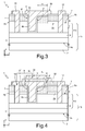
Figure 3 shows, in lateral sectional view, an HEMT device according to a further embodiment of the present disclosure; -
Figure 4 shows, in lateral sectional view, an HEMT device according to a further embodiment of the present disclosure; -
Figure 5 shows, in lateral sectional view, an HEMT device according to a further embodiment of the present disclosure; -
Figures 6A-6E show, in lateral sectional views, successive manufacturing steps of the HEMT device ofFigure 1 ; and -
Figure 7 shows the plot of the drain current of the HEMT device ofFigure 1 in different conditions of drain voltage, compared with an HEMT device according to the known art. -
Figure 1 shows, in a triaxial system of axes X, Y, Z orthogonal to one another, anHEMT device 1 of a normally-off type, based upon gallium nitride, including asubstrate 2, made, for example, of silicon, or silicon carbide (SiC) or sapphire (Al2O3); abuffer layer 3, of gallium and aluminium nitride (AlGaN) or of gallium and indium nitride (InGaN) or, in general, of AlGaN or InGaN alloys, which extends over thesubstrate 2 and is designed to enable a better depletion of the two-dimensional electron gas (2DEG) in the overlying conductive channel; achannel layer 4, of gallium nitride (GaN) or intrinsic InGaN, which extends over thebuffer layer 3 and has a thickness comprised between approximately 10 nm and 2 µm, approximately 1 µm; abarrier layer 6, of intrinsic aluminium and gallium nitride (AlGaN) or, more in general, of compounds based upon ternary or quaternary alloys of gallium nitride, such as AlxGa1-xN, AlInGaN, InxGa1-xN, AlxIn1-xAl, which extends over thechannel layer 4 and has a thickness comprised between approximately 5 nm and 400 nm, e.g. approximately 15 nm; aninsulation layer 7, of dielectric material such as silicon nitride (Si3N4) or silicon oxide (SiO2), which extends over afront side 6a of thebarrier layer 6; and agate region 8, which extends in thesemiconductor body 3 between asource region 10 and adrain region 12. - The
substrate 2, thebuffer layer 3, thechannel layer 4, thebarrier layer 6, and theinsulation layer 7 lie in respective planes parallel to the plane XY and are stacked on one another in the direction Z. - The
channel layer 4 and thebarrier layer 6 form aheterostructure 13. Thesubstrate 2, thebuffer layer 3, and theheterostructure 13 are defined, as a whole, by the term "semiconductor body 15". - The
gate region 8 is separated and insulated laterally (i.e., along X) by thesource region 10 anddrain region 12 by respective portions of theinsulation layer 7. Thegate region 8 is of a recessed type; i.e., it extends in depth through theinsulation layer 7 and completely through thebarrier layer 6, as far as thechannel layer 4. - In other words, the
gate region 8 is formed in atrench 9 dug through theinsulation layer 7 and thebarrier layer 6. - A gate
dielectric layer 8a extends in thetrench 9 facing the bottom and the side walls of thetrench 9. The gate dielectric 8a may further extend, optionally, outside of thetrench 9, i.e., on theinsulation layer 7. Agate metallization 8b completes filling of thetrench 9 and extends over the gatedielectric layer 8a. The gatedielectric layer 8a and thegate metallization 8b form thegate region 8 of theHEMT device 1. - The
gate region 8 has a first side 8' facing thedrain region 12 and asecond side 8" facing thesource region 10. The first andsecond sides 8', 8" of thegate region 8 extend, at least in part, parallel to one another and to the plane XY. - According to one aspect of the present disclosure, an
auxiliary channel 20 extends over afront side 6a of thebarrier layer 6 between, and electrically coupled to, thesource region 10 and thedrain region 12. In particular, theauxiliary channel 20 extends between the first side 8' of thegate region 8 and thedrain region 12, and between thesecond side 8" of thegate region 8 and thesource region 10. However, the portion of auxiliary channel that extends between thegate region 8 and thesource region 10 may be absent. - In even greater detail, the
auxiliary channel 20 extends between, and in contact with, a portion of thesource region 10 and a respective portion of thegate oxide 8a that defines thesecond side 8" of thegate region 8, and further in direct contact with thedrain region 12. However, theauxiliary channel 20 is not in direct contact with the first side 8' of thegate region 8, but at a distance therefrom. Thus, theauxiliary channel 20 extends in the proximity of the first side 8' without ever being in direct contact therewith. Theauxiliary channel 20 extends at a distance d1 (measured in the direction X) from the first side 8' of thegate region 8 chosen so that the electrical field is not excessively high on the first side 8'. An electrical field is considered too high if it causes, or may cause, breakdown of the gate dielectric. - The present applicant has found that values of the distance d1 equal to, or greater than, 0.5 µm are sufficient to satisfy the aforementioned conditions for the choice of d1.
- According to one embodiment of the present disclosure, in the presence of a
gate field plate 30, theauxiliary channel 20 extends laterally staggered with respect to the metal layer that provides thefield plate 30 by a maximum distance (measured along X) not greater than a value d2. The value of distance d2 is chosen so that there do not arise the problems, discussed with reference to the known art, of depletion of the two-dimensional gas (2DEG) and increase of the ON-state resistance as a result of the trapping phenomena. The exact choice of d2 may be made experimentally, by experimental tests on a test device. - The present applicant has found that values of the distance d2 equal to, or smaller than, 0.5 µm are such as to overcome the drawbacks of the known art.
- The
auxiliary channel 20, according to one embodiment, is made of gallium nitride (GaN) with an N-type doping, in particular with a density of dopant species comprised between 1·1018 cm-3 and 1·1019 cm-3, in particular 1·1018 cm-3. In this case, the thickness of theauxiliary channel 20 is comprised between 5 nm and 100 nm, in particular 50 nm. - According to an alternative embodiment, shown in detail in
Figure 2 , theauxiliary channel 20 is a heterostructure including a layer of gallium and aluminium nitride (AlGaN) 22 overlying a layer of gallium nitride (GaN) 24. The AlGaNlayer 22 has a thickness comprised between 5 nm and 50 nm, with aluminium concentration comprised between 15% and 50% (for example, 25%); theGaN layer 24 has a thickness comprised between 2 nm and 50 nm, for example 8 nm. - With reference to the
barrier layer 6, in both of the embodiments ofFigures 1 and 2 , it is preferably formed by twointermediate AlGaN layers 6', 6" having concentrations of aluminium different from one another. According to an aspect of the present disclosure, the concentration of aluminium in the secondintermediate layer 6" is lower than the concentration of aluminium in the first intermediate layer 6'. In particular, the first intermediate layer 6', which extends in direct contact with the channel layer, is made of AlGaN with a concentration of aluminium comprised between 10% and 40%, for example 25%, whereas the secondintermediate layer 6", which extends directly over the first intermediate layer 6', is made of AlGaN with a concentration of aluminium lower than the previous one, namely, comprised between 5% and 30%, for example 15%, or else with a profile of concentration of aluminium decreasing in the direction Z moving away from the first intermediate layer 6' (e.g., 30% of aluminium at the interface with the first intermediate layer 6' and 5% of aluminium at thefront side 6a). The secondintermediate layer 6" further includes silicon doped with N-type dopant species. - This conformation of the
barrier layer 6 enables reduction of the barrier between theauxiliary channel 20 and thebarrier layer 6. - During operation of the
HEMT 1, the charge carriers flow from thesource region 10 to thedrain region 12, following the conductive paths designated by P1 and P2 inFigure 1 . As may be noted, in the portion of active area comprised between thegate region 8 and thesource region 10, the conductive paths P1 and P2 coincide; instead, in the portion of active area comprised between thegate region 8 and thedrain region 12, the conductive paths P1 and P2 do not coincide. Here, part of the charge carriers flows towards thedrain region 12 passing through the two-dimensional electron gas (2DEG) in the channel 4 (path P1), whereas part of the charge carriers flows towards thedrain region 12 passing through the two-dimensional gas (2DEG) in thechannel 4, thebarrier layer 6, and theauxiliary channel 20. - The choice, by the charge carriers, of the conductive path P1 or P2 is a function of the electrical resistance encountered in said path by the charge carriers.
- In the case of undesired increase of the resistance RON in the channel layer 4 (as a result of the known trapping phenomena) the conductive path P2 is privileged over the conductive path P1. In this way, during switching operating conditions of the
HEMT 1 where, as a result of the traps in thechannel layer 4, the resistance RON increases, there always exists an alternative path for the current, i.e., the one offered by theauxiliary channel 20. - Operation of the
HEMT device 1 is thus not inhibited by the traps in thechannel layer 4. - The distance d1 between the first side 8' of the
gate region 8 and theauxiliary channel 20 guarantees that, at the operating voltages considered (e.g., 400 and 600 V), the electrical field at thegate region 8 is not of an excessively high value such as to break thegate oxide 8a. - According to a further aspect of the present disclosure, illustrated in
Figure 3 , the HEMT 1 (according to any of the embodiments ofFigure 1 or Figure 2 ) further has a field-plate metal layer 30, which extends as prolongation of thegate metallization 8b towards thedrain region 12 until it overlies (in top plan view or, equivalently, in the direction Z) theauxiliary channel 20. Theauxiliary channel 20 and the field-plate metal layer 30 are separated from one another by theinsulation layer 7 and, if present, thegate dielectric 8a. - As an alternative to the field-
plate metal layer 30 of a gate-connected type, there may be present one or more field plates of the source-connected type, i.e., electrically coupled to the metallization of thesource region 10, as illustrated inFigure 5 (a source-connected field plate is identified by the reference number 34). - With reference to
Figure 4 , the field-plate metal layer 34 extends between thegate region 8 and thedrain region 12 in parallel to theauxiliary channel 20, until it overlaps the latter (in top plan view or, equivalently, in the direction Z). Theauxiliary channel 20 and the field-plate metal layer 34 are separated from one another by theinsulation layer 7, by apassivation layer 32 and, if present, by thegate dielectric 8a. Thepassivation layer 32 has the function of insulating electrically the field-plate metal layer 34 from thegate region 8. - According to a further embodiment shown in
Figure 5 , theauxiliary channel 20 extends laterally staggered (in the direction X) with respect to the field-plate metal layer 34, i.e., not overlapping it (in the direction Z). - In this case, the maximum distance, measured in the direction X, between the edge that delimits the end of the field-
plate metal layer 34 and the edge that defines the start of theauxiliary channel 20 is d3 and has a value chosen so that there is not created a 2DEG region excessively depleted from the traps present in the buffer. - The value of d3 is, in particular, equal to, or less than, 0.5 µm.
- When both the
gate field plate 30 and thesource field plate 34 are present, theauxiliary channel 20 extends so that it is in at least one of the two conditions mentioned above with reference toFigures 3-4 , i.e., that (i) theauxiliary channel 20 at least partially overlaps one between thegate field plate 30 and thesource field plate 34; and/or (ii) theauxiliary channel 20 extends staggered with respect to both the gate field plate and thesource field plate gate field plate 30 and thesource field plate 34. - Described in what follows, with reference to
Figures 6A-6E , are steps for manufacturing theHEMT device 1 ofFigure 1 . -
Figure 6A shows, in cross-sectional view, a portion of awafer 50 during a step for manufacturing the HEMT device, according to one embodiment of the present invention. Elements of thewafer 50 that are common to the ones already described with reference toFigure 1 and shown inFigure 1 , are designated by the same reference numbers and are not described in detail any further. - In particular, the
wafer 50 is provided, comprising: thesubstrate 2, made, for example, of silicon (Si) or silicon carbide (SiC) or aluminium oxide (Al2O3), having afront side 2a and arear side 2b opposite to one another in a direction Z; thebuffer layer 3 on thefront side 2a of thesubstrate 2, of aluminium and gallium nitride (AlGaN) or of gallium and indium nitride (InGaN); thechannel layer 4, of gallium nitride (GaN), having itsown underside 4a that extends adjacent to, and overlying, thebuffer layer 3; and thebarrier layer 6, which extends over thechannel layer 4. Thebarrier layer 6 and thechannel layer 4 form theheterostructure 13. - According to the present disclosure, formation of the
barrier layer 6 envisages: formation of a first intermediate layer 6' on the channel layer by depositing AlGaN (e.g., via MOCVD or MBE) until a thickness is reached comprised between 5 nm and 20 nm, for example, 8 nm; and formation of a secondintermediate layer 6" by depositing AlGaN and doped silicon with a doping level of 1·1018 cm-3 on the first intermediate layer 6', until a thickness comprised between 5 nm and 20 nm, for example 8 nm, is reached. - During deposition of the first intermediate layer 6', the concentration of aluminium is adjusted so that it is comprised between 10% and 40%; during deposition of the second
intermediate layer 6", the concentration of aluminium is adjusted so that it is comprised between 50% and 30%. - Alternatively, the second
intermediate layer 6" is formed so that it has a profile of concentration of aluminium decreasing in the direction Z moving away from the first intermediate layer 6' (e.g., 30% of aluminium at the interface with the first intermediate layer 6' and 5% of aluminium at thefront side 6a). - Next, on the
front side 6a of thebarrier layer 6 anauxiliary channel layer 56 is formed, for example by depositing gallium nitride, GaN, with N-type doping (e.g., by MOCVD or MBE), according to the embodiment already described with reference toFigure 1 . - Alternatively, according to the embodiment of
Figure 2 , theauxiliary channel layer 56 is formed by depositing a first layer of gallium nitride (GaN), of an intrinsic type and, then, over it, an AlGaN layer. Deposition of both the GaN layer and the AlGaN layer that form theauxiliary channel layer 56 is carried out by deposition (e.g., via MOCVD or MBE), modulating selectively the desired amount of aluminium in both layers. - Then (
Figure 6B ), a step of masked etching of theauxiliary channel layer 56 is carried out to remove first selective portions thereof at a region 57' where, in subsequent machining steps, thegate trench 9 will be formed, and to remove further second selective portions of theauxiliary channel layer 56 that extend alongside the region 57' for a length, in the direction X, equal to d1 (region 57" identified inFigure 6B ). In particular, the removed second selective portions of theauxiliary channel layer 56 extend as lateral prolongation of the first selective regions, towards the portion ofwafer 50 that will house the drain region of theHEMT device 1. This process step defines the distance d1 between thedrain region 8 and theauxiliary channel 20, as described previously. - Then, once again with reference to
Figure 6B , formed on the wafer 50 (and thus on theauxiliary channel layer 56 thus structured and at theregions 57', 57") is apassivation layer 52, of dielectric or insulating material, for example silicon nitride (SiN) or silicon oxide (SiO2). Thepassivation layer 52 has a thickness comprised between 5 nm and 300 nm, for example 100 nm, and is formed by CVD or atomic-layer deposition (ALD), and, at the end of the manufacturing steps, will form theinsulation layer 7. - Next (
Figure 6C ), thepassivation layer 52 is selectively removed, for example by lithographic and etching steps, for removing selective portions thereof in the region 57' of thewafer 50 where thegate region 8 of theHEMT device 1 is to be formed. - The etching step may stop at the underlying barrier layer 6 (to provide an HEMT of a normally-on type), or else it may proceed partially into the barrier layer 6 (the latter embodiment is shown in
Figure 6B ). In this second case, a surface portion 4' of theunderlying channel layer 4 is exposed. Etching of thebarrier layer 6 is carried out, for example, by dry etching. - The
trench 9 is thus formed, which extends throughout the thickness of thepassivation layer 52 and for an underlying portion of thebarrier layer 6. - There is then formed, for example by deposition, the gate-
dielectric layer 8a, made, for example, of a material chosen from among aluminium nitride (AlN), silicon nitride (SiN), aluminium oxide (Al2O3), and silicon oxide (SiO2). The gate-dielectric layer 8a has a thickness chosen between 1 and 50 nm, for example 20 nm. - Next (
Figure 6D ), a step of deposition of conductive material on thewafer 30 is carried out to form aconductive layer 58 on thegate dielectric layer 8a, in particular in order to fill thetrench 9. For example, theconductive layer 58 is made of metal material, such as tantalum (Ta), tantalum nitride (TaN), titanium nitride (TiN), palladium (Pa), tungsten (W), tungsten silicide (WSi2), titanium/aluminium (Ti/Al), or nickel/gold (Ni/Au). - The
conductive layer 58 is then selectively removed by lithographic and etching steps in themselves known for eliminating it from thewafer 50 except for the portion thereof that extends in thetrench 9, thus forming thegate metallization 8b. During the same step, using an appropriate mask for etching of theconductive layer 58, it is further possible to define, in a per se known manner, thegate field plate 30, described with reference toFigure 3 . - The
gate metallization 8b and thegate dielectric 8a form, as a whole, therecessed-gate region 8 of the HEMT device ofFigure 1 . - Then (
Figure 6E ), one or more further steps of masked etching of thegate dielectric 8a, of thepassivation layer 52, of theauxiliary channel layer 56, and of thebarrier layer 6 are carried out to remove selective portions thereof that extend in regions of thewafer 50 where the source andgate regions HEMT device 1 are to be formed. - Removal of the selective portions of the
passivation layer 52 leads to formation of theinsulation layer 7 illustrated inFigure 1 . Likewise, removal of selective portions of theauxiliary channel layer 56 leads to formation of theauxiliary channel 20 illustrated inFigure 1 . - In particular, openings are formed on opposite sides (
sides 8' and 8") of thegate region 8, and at a distance from thegate region 8, until thechannel layer 4 is reached. - Next, a step of formation of ohmic contacts is carried out to provide the source and drain
regions wafer 50. A next step of etching of the metal layer thus deposited is then carried out to remove said metal layer from thewafer 50 except for the metal portions that extend within source and drain openings to form therein thesource region 10 and thedrain region 12, respectively. - Next, a step of rapid thermal annealing (RTA), for example at a temperature comprised between approximately 500 and 900°C for a time of from 20 s to 5 min, enables formation of electrode ohmic contacts of the
source region 10 and drainregion 12 with the underlying channel layer (having the two-dimensional gas 2DEG). - The
HEMT device 1 shown inFigure 1 is thus formed. -
Figure 7 represents the plot (obtained by simulation) of the drain current (which is indicative of the ON-state resistance RON) as a function of the drain stresses, for two biasing values provided by way of example (400 V and 600 V), and in both the case where the auxiliary channel is present according to the present disclosure and in the case where the auxiliary channel is absent according to the prior art. In particular, with reference toFigure 7 : - the curve C1 shows the plot of the drain voltage as a function of the drain current in pre-stress conditions in an HEMT device provided with the
auxiliary channel 20, according to the present disclosure; - the curve C2 shows the plot of the drain voltage as a function of the drain current in pre-stress conditions in an HEMT device according to the known art, without of the
auxiliary channel 20; - the curve C3 represents the plot of the drain voltage as a function of the drain current in post-stress conditions (400 V) in an HEMT device provided with the
auxiliary channel 20, according to the present disclosure; - the curve C4 represents the plot of the drain voltage as a function of the drain current in post-stress conditions (400 V) in an HEMT device according to the known art, without the
auxiliary channel 20; - the curve C5 represents the plot of the drain voltage as a function of the drain current in post-stress conditions (600 V) in an HEMT device provided with the
auxiliary channel 20, according to the present disclosure; and - the curve C6 represents the plot of the drain voltage as a function of the drain current in post-stress conditions (600 V) in an HEMT device according to the known art, without the
auxiliary channel 20. - As may be noted, the presence of the auxiliary channel 20 (curves C1, C3, C5) determines a marked increase in the drain current as compared to an embodiment that does not envisage it (curves C2, C4, C6), in operating conditions comparable to one another.
- Consequently, according to the present disclosure, the operating and functional characteristics of the
HEMT device 1 are improved as compared to what is available according to the prior art. - An HEMT device provided according to the present invention shows high values of current irrespective of the operating conditions, and irrespective of the traps present in the channel layer (which does not require any specific optimization for reduction of the traps). The performance of the device is markedly improved.
- Finally, it is clear that modifications and variations may be made to what is described and illustrated herein, without thereby departing from the scope of the present invention, as defined in the annexed claims.
- For example, according to further embodiments (not shown), the semiconductor body 5 may comprise, if need be, just one or else more than one layers of GaN, or GaN alloys, appropriately doped or of an intrinsic type.
- Further, according to one embodiment, the
source region 10 and thedrain region 12 extend in depth in the semiconductor body 5, completely through thebarrier layer 6 and partially through thechannel layer 4, and terminate within thechannel layer 4.
Alternatively, the metallizations of the source and drain contacts may further be provided only partially recessed within thebarrier layer 6, or else facing thefront side 6a of thebarrier layer 6. - The metallizations of the source, drain, and gate contacts may be made using any material designed for the purpose, such as, for example, formation of contacts of AlSiCu/Ti, Al/Ti, or W-plug, etc.
- Further, according to one embodiment, the
gate region 8 does not extend completely through thebarrier layer 6, but terminates at thefront side 6a of the barrier layer; in this case, the HEMT device is of a normally-on type.
Claims (18)
- An HEMT device (1), comprising:a semiconductor body (15) including a heterojunction structure (13) that forms a main conductive channel (4) of the HEMT device (1);a dielectric layer (7) on the semiconductor body;a gate electrode (8), a drain electrode (12), and a source electrode (10) aligned to one another in a direction (X), wherein the drain electrode (12) extends facing a first side (8') of the gate electrode (8), and the source electrode extends facing a second side (8"), opposite to the first side in said direction (X), of the gate electrode,characterized by further comprising an auxiliary channel layer (20), which extends over the heterojunction structure (13) between the gate electrode (8) and the drain electrode (12), in electrical contact with the drain electrode (12) and at a distance from the gate electrode (8), and forms a conductive path additional to the main conductive channel (4) for charge carriers that flow between the source electrode and the drain electrode.
- The HEMT device according to claim 1, wherein the auxiliary channel layer (20) extends at a distance from first side (8') of the gate electrode (8) that is equal to, or greater than, 0.5 µm along said direction (X).
- The HEMT device according to claim 1 or claim 2, wherein the auxiliary channel layer (2) is of gallium nitride with N-type doping.
- The HEMT device according to claim 1 or claim 2, wherein the auxiliary channel layer (20) includes a layer of gallium and aluminium nitride, having a concentration of aluminium comprised between 10% and 40%, which extends over a layer of gallium nitride having a concentration of aluminium comprised between 5% and 30%.
- The HEMT device according to any one of the preceding claims, wherein the heterojunction structure (13) comprises: a channel layer (4), of a first material, and a barrier layer (6), of a second material, extending over the channel layer (4), the first and second materials having different band gap,
and wherein the barrier layer (6) includes: a first intermediate layer (6') including gallium and aluminium nitride having a concentration of aluminium comprised between 10% and 40%, and a second intermediate layer (6"), which extends over the first intermediate layer (6'), including gallium and aluminium nitride having a concentration of aluminium comprised between 5% and 30%. - The HEMT device according to any one of the preceding claims, further comprising a field plate (30) which extends over the dielectric layer (7) and overlaps, at least in part, the auxiliary channel layer (20).
- The HEMT device according to any one of claims 1-5, further comprising a field plate (30), which extends over the dielectric layer (7), wherein the field plate extends further at a distance, along said direction (X), from the auxiliary channel layer (20).
- The HEMT device according to claim 7, wherein said distance is equal to, or less than, 0.5 µm.
- The HEMT device according to any one of claims 6-8, wherein said field plate is either a gate field plate, electrically coupled to the gate electrode (8), or a source field plate, electrically coupled to the source electrode (10).
- A method of manufacturing of an HEMT device (1), comprising the steps of:forming a heterojunction structure (13) in a semiconductor body (15) thus defining a main conductive channel (4) of the HEMT device (1);forming a dielectric layer (7) on the semiconductor body;forming a gate electrode (8), including forming a conductive gate region (8b) and a gate dielectric (8a) that insulates electrically the conductive gate region (8b) from the semiconductor body;forming a drain electrode (12) and a source electrode (10) aligned to one another and to the gate electrode in a direction (X), wherein the drain electrode is formed facing a first side (8') of the gate electrode, and the source electrode is formed facing a second side (8"), opposite to first side in said direction (X), of the gate electrode,characterized in that it further comprises the step of forming an auxiliary channel layer (20) on the heterojunction structure (13) between the gate electrode (8) and the drain electrode (12), in electrical contact with the drain electrode (12) and at a distance from the gate electrode (8), thus forming a conductive path, additional to the main conductive channel (4), for charge carriers that flow between the source electrode and the drain electrode.
- The method according to claim 10, wherein the step of forming the auxiliary channel layer (20) comprises forming the auxiliary channel layer (20) at a distance the from first side (8') of the gate electrode (8) equal to, or greater than, 0.5 µm along said direction (X).
- The method according to claim 10 or claim 11, wherein forming the auxiliary channel layer (20) comprises depositing a layer of gallium nitride with N-type doping.
- The method according to claim 10 or claim 11, wherein forming the auxiliary channel layer (20) comprises depositing a layer of gallium nitride having a concentration of aluminium comprised between 20% and 30% and, then, depositing a layer of gallium and aluminium nitride, having a concentration of aluminium comprised between 10% and 20%.
- The method according to any one of claims 10-13, wherein forming the heterojunction structure (13) comprises:depositing a channel layer (4), of a first material, and depositing a barrier layer (6), of a second material, on the channel layer (4), the first and second materials having different band gaps,and wherein forming the barrier layer (6) includes: depositing a first intermediate layer (6') of gallium and aluminium nitride having a concentration of aluminium comprised between 20% and 30%, and depositing a second intermediate layer (6"), on the first intermediate layer (6'), of gallium and aluminium nitride having a concentration of aluminium comprised between 10% and 20%.
- The method according to any one of the preceding claims, further comprising forming a field plate (30) on the dielectric layer (7) and overlapping, at least in part, to the auxiliary channel layer (20).
- The method according to any one of claims 10-14, further comprising forming a field plate (30) on the dielectric layer (7), at a distance, along said direction (X), from the auxiliary channel layer (20).
- The method according to claim 16, wherein said distance is equal to, or less than, 0.5 µm.
- The method according to any one of claims 15-17, wherein forming said field plate includes either of the following steps: forming a gate field plate electrically coupled to the gate electrode (8); or forming a source field plate electrically coupled to the source electrode (10).
Priority Applications (8)
| Application Number | Priority Date | Filing Date | Title |
|---|---|---|---|
| EP16425047.4A EP3252825B1 (en) | 2016-05-30 | 2016-05-30 | Double-channel hemt device and manufacturing method thereof |
| CN201611052945.3A CN107452791B (en) | 2016-05-30 | 2016-11-25 | Dual-channel HEMT device and method of making the same |
| CN201621274262.8U CN206412367U (en) | 2016-05-30 | 2016-11-25 | High electron mobility transistor (HEMT) device |
| US15/393,945 US10381470B2 (en) | 2016-05-30 | 2016-12-29 | Double-channel HEMT device and manufacturing method thereof |
| US16/431,642 US10892357B2 (en) | 2016-05-30 | 2019-06-04 | Double-channel HEMT device and manufacturing method thereof |
| US17/115,459 US11489068B2 (en) | 2016-05-30 | 2020-12-08 | Double-channel HEMT device and manufacturing method thereof |
| US17/977,971 US12148823B2 (en) | 2016-05-30 | 2022-10-31 | Double-channel HEMT device and manufacturing method thereof |
| US18/912,488 US20250040173A1 (en) | 2016-05-30 | 2024-10-10 | Double-channel hemt device and manufacturing method thereof |
Applications Claiming Priority (1)
| Application Number | Priority Date | Filing Date | Title |
|---|---|---|---|
| EP16425047.4A EP3252825B1 (en) | 2016-05-30 | 2016-05-30 | Double-channel hemt device and manufacturing method thereof |
Publications (2)
| Publication Number | Publication Date |
|---|---|
| EP3252825A1 true EP3252825A1 (en) | 2017-12-06 |
| EP3252825B1 EP3252825B1 (en) | 2022-12-21 |
Family
ID=56799387
Family Applications (1)
| Application Number | Title | Priority Date | Filing Date |
|---|---|---|---|
| EP16425047.4A Active EP3252825B1 (en) | 2016-05-30 | 2016-05-30 | Double-channel hemt device and manufacturing method thereof |
Country Status (3)
| Country | Link |
|---|---|
| US (5) | US10381470B2 (en) |
| EP (1) | EP3252825B1 (en) |
| CN (2) | CN206412367U (en) |
Families Citing this family (18)
| Publication number | Priority date | Publication date | Assignee | Title |
|---|---|---|---|---|
| EP3252825B1 (en) | 2016-05-30 | 2022-12-21 | STMicroelectronics S.r.l. | Double-channel hemt device and manufacturing method thereof |
| US10637460B2 (en) | 2016-06-14 | 2020-04-28 | Macom Technology Solutions Holdings, Inc. | Circuits and operating methods thereof for monitoring and protecting a device |
| US20180109228A1 (en) | 2016-10-14 | 2018-04-19 | MACOM Technology Solution Holdings, Inc. | Phase shifters for gallium nitride amplifiers and related methods |
| US20190028066A1 (en) * | 2017-07-24 | 2019-01-24 | Macom Technology Solutions Holdings, Inc. | Fet operational temperature determination by field plate resistance thermometry |
| US20190028065A1 (en) * | 2017-07-24 | 2019-01-24 | Macom Technology Solutions Holdings, Inc. | Fet operational temperature determination by gate structure resistance thermometry |
| US10418474B2 (en) * | 2017-10-17 | 2019-09-17 | Mitsubishi Electric Research Laboratories, Inc. | High electron mobility transistor with varying semiconductor layer |
| US11121229B2 (en) | 2017-12-28 | 2021-09-14 | Vanguard International Semiconductor Corporation | Methods of fabricating semiconductor structures and high electron mobility transistors |
| CN111868931B (en) * | 2018-02-14 | 2024-03-12 | Hrl实验室有限责任公司 | Highly scalable linear GaN HEMT structures |
| US11316038B2 (en) | 2018-11-20 | 2022-04-26 | Stmicroelectronics S.R.L. | HEMT transistor with adjusted gate-source distance, and manufacturing method thereof |
| CN111834435B (en) * | 2019-04-15 | 2025-03-25 | 联华电子股份有限公司 | High Electron Mobility Transistor |
| US11335797B2 (en) * | 2019-04-17 | 2022-05-17 | Vanguard International Semiconductor Corporation | Semiconductor devices and methods for fabricating the same |
| IT201900023475A1 (en) * | 2019-12-10 | 2021-06-10 | St Microelectronics Srl | HEMT TRANSISTOR INCLUDING FIELD PLATE REGIONS AND RELATED MANUFACTURING PROCESS |
| US11855198B2 (en) * | 2020-04-09 | 2023-12-26 | Qualcomm Incorporated | Multi-gate high electron mobility transistors (HEMTs) employing tuned recess depth gates for improved device linearity |
| CN114649409A (en) * | 2020-12-18 | 2022-06-21 | 华为技术有限公司 | High electron mobility transistor, preparation method and power amplifier/switch |
| CN115440808A (en) * | 2021-06-04 | 2022-12-06 | 联华电子股份有限公司 | Nitride semiconductor element and method for manufacturing the same |
| CN113644129B (en) * | 2021-08-12 | 2023-04-25 | 电子科技大学 | A reverse-resistance HEMT with a stepped P-type GaN drain structure |
| CN116072722A (en) * | 2021-10-29 | 2023-05-05 | 苏州晶湛半导体有限公司 | Enhanced semiconductor structure and fabrication method thereof |
| CN115332335B (en) * | 2022-08-26 | 2026-03-24 | 电子科技大学 | A vertical GaN HEMT power device |
Citations (4)
| Publication number | Priority date | Publication date | Assignee | Title |
|---|---|---|---|---|
| US6274893B1 (en) * | 1998-06-15 | 2001-08-14 | Fujitsu Quantum Devices Limited | Compound semiconductor device and method of manufacturing the same |
| CN102130158A (en) * | 2011-01-05 | 2011-07-20 | 西安电子科技大学 | Step-like groove-grid high electron mobility transistor |
| CN102629624A (en) * | 2012-04-29 | 2012-08-08 | 西安电子科技大学 | Metal-insulator-semiconductor (MIS) grid enhanced high electron mobility transistor (HEMT) device based on gallium nitride (GaN) and manufacture method of MIS grid enhanced HEMT device |
| CN102637726A (en) * | 2012-04-29 | 2012-08-15 | 西安电子科技大学 | MS (Metal-Semiconductor)-grid GaN-based enhanced transistor with high electron mobility and manufacture method thereof |
Family Cites Families (19)
| Publication number | Priority date | Publication date | Assignee | Title |
|---|---|---|---|---|
| JP4997660B2 (en) * | 1999-10-29 | 2012-08-08 | 富士通株式会社 | Semiconductor device |
| US6521961B1 (en) * | 2000-04-28 | 2003-02-18 | Motorola, Inc. | Semiconductor device using a barrier layer between the gate electrode and substrate and method therefor |
| US7932539B2 (en) * | 2005-11-29 | 2011-04-26 | The Hong Kong University Of Science And Technology | Enhancement-mode III-N devices, circuits, and methods |
| US8338861B2 (en) * | 2007-01-10 | 2012-12-25 | International Rectifier Corporation | III-nitride semiconductor device with stepped gate trench and process for its manufacture |
| JP2011082216A (en) * | 2009-10-02 | 2011-04-21 | Fujitsu Ltd | Compound semiconductor device and method for manufacturing the same |
| KR101736914B1 (en) * | 2010-12-06 | 2017-05-19 | 한국전자통신연구원 | Method of manufacturing high frequency device structures |
| JP5648523B2 (en) * | 2011-02-16 | 2015-01-07 | 富士通株式会社 | Semiconductor device, power supply device, amplifier, and semiconductor device manufacturing method |
| US10312361B2 (en) * | 2011-06-20 | 2019-06-04 | The Regents Of The University Of California | Trenched vertical power field-effect transistors with improved on-resistance and breakdown voltage |
| US20130105817A1 (en) * | 2011-10-26 | 2013-05-02 | Triquint Semiconductor, Inc. | High electron mobility transistor structure and method |
| JP5864214B2 (en) * | 2011-10-31 | 2016-02-17 | 株式会社日立製作所 | Semiconductor device |
| US9337332B2 (en) * | 2012-04-25 | 2016-05-10 | Hrl Laboratories, Llc | III-Nitride insulating-gate transistors with passivation |
| CN102683406B (en) * | 2012-04-29 | 2014-08-20 | 西安电子科技大学 | GaN-based MS grid enhancement type high electron mobility transistor and manufacture method thereof |
| US9035355B2 (en) * | 2012-06-18 | 2015-05-19 | Infineon Technologies Austria Ag | Multi-channel HEMT |
| US20140159116A1 (en) * | 2012-12-07 | 2014-06-12 | International Rectifier Corporation | III-Nitride Device Having an Enhanced Field Plate |
| US9202906B2 (en) * | 2013-03-14 | 2015-12-01 | Northrop Grumman Systems Corporation | Superlattice crenelated gate field effect transistor |
| JP6220161B2 (en) * | 2013-06-03 | 2017-10-25 | ルネサスエレクトロニクス株式会社 | Manufacturing method of semiconductor device |
| US9614069B1 (en) * | 2015-04-10 | 2017-04-04 | Cambridge Electronics, Inc. | III-Nitride semiconductors with recess regions and methods of manufacture |
| US9419121B1 (en) * | 2015-07-17 | 2016-08-16 | Mitsubishi Electric Research Laboratories, Inc. | Semiconductor device with multiple carrier channels |
| EP3252825B1 (en) * | 2016-05-30 | 2022-12-21 | STMicroelectronics S.r.l. | Double-channel hemt device and manufacturing method thereof |
-
2016
- 2016-05-30 EP EP16425047.4A patent/EP3252825B1/en active Active
- 2016-11-25 CN CN201621274262.8U patent/CN206412367U/en active Active
- 2016-11-25 CN CN201611052945.3A patent/CN107452791B/en active Active
- 2016-12-29 US US15/393,945 patent/US10381470B2/en active Active
-
2019
- 2019-06-04 US US16/431,642 patent/US10892357B2/en active Active
-
2020
- 2020-12-08 US US17/115,459 patent/US11489068B2/en active Active
-
2022
- 2022-10-31 US US17/977,971 patent/US12148823B2/en active Active
-
2024
- 2024-10-10 US US18/912,488 patent/US20250040173A1/en active Pending
Patent Citations (4)
| Publication number | Priority date | Publication date | Assignee | Title |
|---|---|---|---|---|
| US6274893B1 (en) * | 1998-06-15 | 2001-08-14 | Fujitsu Quantum Devices Limited | Compound semiconductor device and method of manufacturing the same |
| CN102130158A (en) * | 2011-01-05 | 2011-07-20 | 西安电子科技大学 | Step-like groove-grid high electron mobility transistor |
| CN102629624A (en) * | 2012-04-29 | 2012-08-08 | 西安电子科技大学 | Metal-insulator-semiconductor (MIS) grid enhanced high electron mobility transistor (HEMT) device based on gallium nitride (GaN) and manufacture method of MIS grid enhanced HEMT device |
| CN102637726A (en) * | 2012-04-29 | 2012-08-15 | 西安电子科技大学 | MS (Metal-Semiconductor)-grid GaN-based enhanced transistor with high electron mobility and manufacture method thereof |
Non-Patent Citations (3)
| Title |
|---|
| D. JIN ET AL.: "Microsystems Technology Laboratories", MASSACHUSETTS INSTITUTE OF TECHNOLOGY, article "Total current collapse in High-Voltage GaN MIS-HEMTs induced by Zener trapping" |
| J. WURFL ET AL., TECHNIQUES TOWARDS GAN POWER TRANSISTORS WITH IMPROVED HIGH VOLTAGE DYNAMIC SWITCHING PROPERTIES, 2013 |
| P. MOENS ET AL., ON THE IMPACT OF CARBON-DOPING ON THE DYNAMIC RON AND OFF-STATE LEAKAGE CURRENT OF 650V GAN POWER DEVICES |
Also Published As
| Publication number | Publication date |
|---|---|
| US11489068B2 (en) | 2022-11-01 |
| EP3252825B1 (en) | 2022-12-21 |
| CN206412367U (en) | 2017-08-15 |
| US20190288100A1 (en) | 2019-09-19 |
| CN107452791B (en) | 2021-07-20 |
| CN107452791A (en) | 2017-12-08 |
| US12148823B2 (en) | 2024-11-19 |
| US10381470B2 (en) | 2019-08-13 |
| US20250040173A1 (en) | 2025-01-30 |
| US20230047815A1 (en) | 2023-02-16 |
| US10892357B2 (en) | 2021-01-12 |
| US20210091218A1 (en) | 2021-03-25 |
| US20170345922A1 (en) | 2017-11-30 |
Similar Documents
| Publication | Publication Date | Title |
|---|---|---|
| US12148823B2 (en) | Double-channel HEMT device and manufacturing method thereof | |
| CN109196650B (en) | Multi-step surface passivation structure and manufacturing method thereof | |
| US12457765B2 (en) | Normally-off transistor with reduced on-state resistance and manufacturing method | |
| CN110233103B (en) | High electron mobility transistor with deep carrier gas contact structure | |
| CN102017160B (en) | Enhanced Mode III-N HEMT | |
| US10840353B2 (en) | High electron mobility transistor with dual thickness barrier layer | |
| EP3657549B1 (en) | Hemt transistor with adjusted gate-source distance, and manufacturing method thereof | |
| KR20180064339A (en) | High-electron-mobility transistor and manufacturing method thereof | |
| EP2713402A2 (en) | Normally-off high electron mobility transistor | |
| US11594625B2 (en) | III-N transistor structures with stepped cap layers | |
| EP2747143A1 (en) | GaN HEMTs and GaN diodes | |
| EP4654780A1 (en) | Normally-off hemt device with improved dynamic performances, and manufacturing method thereof | |
| US20230395650A1 (en) | Nitride semiconductor device and semiconductor package | |
| KR20140061145A (en) | High electron mobility transistor and method of manufacturing the same |
Legal Events
| Date | Code | Title | Description |
|---|---|---|---|
| PUAI | Public reference made under article 153(3) epc to a published international application that has entered the european phase |
Free format text: ORIGINAL CODE: 0009012 |
|
| STAA | Information on the status of an ep patent application or granted ep patent |
Free format text: STATUS: THE APPLICATION HAS BEEN PUBLISHED |
|
| AK | Designated contracting states |
Kind code of ref document: A1 Designated state(s): AL AT BE BG CH CY CZ DE DK EE ES FI FR GB GR HR HU IE IS IT LI LT LU LV MC MK MT NL NO PL PT RO RS SE SI SK SM TR |
|
| AX | Request for extension of the european patent |
Extension state: BA ME |
|
| STAA | Information on the status of an ep patent application or granted ep patent |
Free format text: STATUS: REQUEST FOR EXAMINATION WAS MADE |
|
| 17P | Request for examination filed |
Effective date: 20180605 |
|
| RBV | Designated contracting states (corrected) |
Designated state(s): AL AT BE BG CH CY CZ DE DK EE ES FI FR GB GR HR HU IE IS IT LI LT LU LV MC MK MT NL NO PL PT RO RS SE SI SK SM TR |
|
| STAA | Information on the status of an ep patent application or granted ep patent |
Free format text: STATUS: EXAMINATION IS IN PROGRESS |
|
| 17Q | First examination report despatched |
Effective date: 20210128 |
|
| REG | Reference to a national code |
Ref country code: DE Ref legal event code: R079 Ref document number: 602016076985 Country of ref document: DE Free format text: PREVIOUS MAIN CLASS: H01L0029660000 Ipc: H01L0029060000 |
|
| GRAP | Despatch of communication of intention to grant a patent |
Free format text: ORIGINAL CODE: EPIDOSNIGR1 |
|
| STAA | Information on the status of an ep patent application or granted ep patent |
Free format text: STATUS: GRANT OF PATENT IS INTENDED |
|
| RIC1 | Information provided on ipc code assigned before grant |
Ipc: H01L 29/423 20060101ALN20220617BHEP Ipc: H01L 29/417 20060101ALN20220617BHEP Ipc: H01L 29/778 20060101ALI20220617BHEP Ipc: H01L 29/66 20060101ALI20220617BHEP Ipc: H01L 29/40 20060101ALI20220617BHEP Ipc: H01L 29/205 20060101ALI20220617BHEP Ipc: H01L 29/20 20060101ALI20220617BHEP Ipc: H01L 29/06 20060101AFI20220617BHEP |
|
| RIC1 | Information provided on ipc code assigned before grant |
Ipc: H01L 29/423 20060101ALN20220630BHEP Ipc: H01L 29/417 20060101ALN20220630BHEP Ipc: H01L 29/778 20060101ALI20220630BHEP Ipc: H01L 29/66 20060101ALI20220630BHEP Ipc: H01L 29/40 20060101ALI20220630BHEP Ipc: H01L 29/205 20060101ALI20220630BHEP Ipc: H01L 29/20 20060101ALI20220630BHEP Ipc: H01L 29/06 20060101AFI20220630BHEP |
|
| INTG | Intention to grant announced |
Effective date: 20220714 |
|
| RIN1 | Information on inventor provided before grant (corrected) |
Inventor name: CHINI, ALESSANDRO Inventor name: IUCOLANO, FERDINANDO |
|
| GRAS | Grant fee paid |
Free format text: ORIGINAL CODE: EPIDOSNIGR3 |
|
| GRAA | (expected) grant |
Free format text: ORIGINAL CODE: 0009210 |
|
| STAA | Information on the status of an ep patent application or granted ep patent |
Free format text: STATUS: THE PATENT HAS BEEN GRANTED |
|
| AK | Designated contracting states |
Kind code of ref document: B1 Designated state(s): AL AT BE BG CH CY CZ DE DK EE ES FI FR GB GR HR HU IE IS IT LI LT LU LV MC MK MT NL NO PL PT RO RS SE SI SK SM TR |
|
| REG | Reference to a national code |
Ref country code: GB Ref legal event code: FG4D |
|
| REG | Reference to a national code |
Ref country code: CH Ref legal event code: EP |
|
| REG | Reference to a national code |
Ref country code: DE Ref legal event code: R096 Ref document number: 602016076985 Country of ref document: DE |
|
| REG | Reference to a national code |
Ref country code: AT Ref legal event code: REF Ref document number: 1539576 Country of ref document: AT Kind code of ref document: T Effective date: 20230115 |
|
| REG | Reference to a national code |
Ref country code: IE Ref legal event code: FG4D |
|
| REG | Reference to a national code |
Ref country code: LT Ref legal event code: MG9D |
|
| REG | Reference to a national code |
Ref country code: NL Ref legal event code: MP Effective date: 20221221 |
|
| PG25 | Lapsed in a contracting state [announced via postgrant information from national office to epo] |
Ref country code: SE Free format text: LAPSE BECAUSE OF FAILURE TO SUBMIT A TRANSLATION OF THE DESCRIPTION OR TO PAY THE FEE WITHIN THE PRESCRIBED TIME-LIMIT Effective date: 20221221 Ref country code: NO Free format text: LAPSE BECAUSE OF FAILURE TO SUBMIT A TRANSLATION OF THE DESCRIPTION OR TO PAY THE FEE WITHIN THE PRESCRIBED TIME-LIMIT Effective date: 20230321 Ref country code: LT Free format text: LAPSE BECAUSE OF FAILURE TO SUBMIT A TRANSLATION OF THE DESCRIPTION OR TO PAY THE FEE WITHIN THE PRESCRIBED TIME-LIMIT Effective date: 20221221 Ref country code: FI Free format text: LAPSE BECAUSE OF FAILURE TO SUBMIT A TRANSLATION OF THE DESCRIPTION OR TO PAY THE FEE WITHIN THE PRESCRIBED TIME-LIMIT Effective date: 20221221 |
|
| REG | Reference to a national code |
Ref country code: AT Ref legal event code: MK05 Ref document number: 1539576 Country of ref document: AT Kind code of ref document: T Effective date: 20221221 |
|
| PG25 | Lapsed in a contracting state [announced via postgrant information from national office to epo] |
Ref country code: RS Free format text: LAPSE BECAUSE OF FAILURE TO SUBMIT A TRANSLATION OF THE DESCRIPTION OR TO PAY THE FEE WITHIN THE PRESCRIBED TIME-LIMIT Effective date: 20221221 Ref country code: LV Free format text: LAPSE BECAUSE OF FAILURE TO SUBMIT A TRANSLATION OF THE DESCRIPTION OR TO PAY THE FEE WITHIN THE PRESCRIBED TIME-LIMIT Effective date: 20221221 Ref country code: HR Free format text: LAPSE BECAUSE OF FAILURE TO SUBMIT A TRANSLATION OF THE DESCRIPTION OR TO PAY THE FEE WITHIN THE PRESCRIBED TIME-LIMIT Effective date: 20221221 Ref country code: GR Free format text: LAPSE BECAUSE OF FAILURE TO SUBMIT A TRANSLATION OF THE DESCRIPTION OR TO PAY THE FEE WITHIN THE PRESCRIBED TIME-LIMIT Effective date: 20230322 |
|
| PG25 | Lapsed in a contracting state [announced via postgrant information from national office to epo] |
Ref country code: NL Free format text: LAPSE BECAUSE OF FAILURE TO SUBMIT A TRANSLATION OF THE DESCRIPTION OR TO PAY THE FEE WITHIN THE PRESCRIBED TIME-LIMIT Effective date: 20221221 |
|
| PG25 | Lapsed in a contracting state [announced via postgrant information from national office to epo] |
Ref country code: SM Free format text: LAPSE BECAUSE OF FAILURE TO SUBMIT A TRANSLATION OF THE DESCRIPTION OR TO PAY THE FEE WITHIN THE PRESCRIBED TIME-LIMIT Effective date: 20221221 Ref country code: RO Free format text: LAPSE BECAUSE OF FAILURE TO SUBMIT A TRANSLATION OF THE DESCRIPTION OR TO PAY THE FEE WITHIN THE PRESCRIBED TIME-LIMIT Effective date: 20221221 Ref country code: PT Free format text: LAPSE BECAUSE OF FAILURE TO SUBMIT A TRANSLATION OF THE DESCRIPTION OR TO PAY THE FEE WITHIN THE PRESCRIBED TIME-LIMIT Effective date: 20230421 Ref country code: ES Free format text: LAPSE BECAUSE OF FAILURE TO SUBMIT A TRANSLATION OF THE DESCRIPTION OR TO PAY THE FEE WITHIN THE PRESCRIBED TIME-LIMIT Effective date: 20221221 Ref country code: EE Free format text: LAPSE BECAUSE OF FAILURE TO SUBMIT A TRANSLATION OF THE DESCRIPTION OR TO PAY THE FEE WITHIN THE PRESCRIBED TIME-LIMIT Effective date: 20221221 Ref country code: CZ Free format text: LAPSE BECAUSE OF FAILURE TO SUBMIT A TRANSLATION OF THE DESCRIPTION OR TO PAY THE FEE WITHIN THE PRESCRIBED TIME-LIMIT Effective date: 20221221 Ref country code: AT Free format text: LAPSE BECAUSE OF FAILURE TO SUBMIT A TRANSLATION OF THE DESCRIPTION OR TO PAY THE FEE WITHIN THE PRESCRIBED TIME-LIMIT Effective date: 20221221 |
|
| PG25 | Lapsed in a contracting state [announced via postgrant information from national office to epo] |
Ref country code: SK Free format text: LAPSE BECAUSE OF FAILURE TO SUBMIT A TRANSLATION OF THE DESCRIPTION OR TO PAY THE FEE WITHIN THE PRESCRIBED TIME-LIMIT Effective date: 20221221 Ref country code: PL Free format text: LAPSE BECAUSE OF FAILURE TO SUBMIT A TRANSLATION OF THE DESCRIPTION OR TO PAY THE FEE WITHIN THE PRESCRIBED TIME-LIMIT Effective date: 20221221 Ref country code: IS Free format text: LAPSE BECAUSE OF FAILURE TO SUBMIT A TRANSLATION OF THE DESCRIPTION OR TO PAY THE FEE WITHIN THE PRESCRIBED TIME-LIMIT Effective date: 20230421 Ref country code: AL Free format text: LAPSE BECAUSE OF FAILURE TO SUBMIT A TRANSLATION OF THE DESCRIPTION OR TO PAY THE FEE WITHIN THE PRESCRIBED TIME-LIMIT Effective date: 20221221 |
|
| REG | Reference to a national code |
Ref country code: DE Ref legal event code: R097 Ref document number: 602016076985 Country of ref document: DE |
|
| PLBE | No opposition filed within time limit |
Free format text: ORIGINAL CODE: 0009261 |
|
| STAA | Information on the status of an ep patent application or granted ep patent |
Free format text: STATUS: NO OPPOSITION FILED WITHIN TIME LIMIT |
|
| PG25 | Lapsed in a contracting state [announced via postgrant information from national office to epo] |
Ref country code: DK Free format text: LAPSE BECAUSE OF FAILURE TO SUBMIT A TRANSLATION OF THE DESCRIPTION OR TO PAY THE FEE WITHIN THE PRESCRIBED TIME-LIMIT Effective date: 20221221 |
|
| 26N | No opposition filed |
Effective date: 20230922 |
|
| REG | Reference to a national code |
Ref country code: CH Ref legal event code: PL |
|
| PG25 | Lapsed in a contracting state [announced via postgrant information from national office to epo] |
Ref country code: MC Free format text: LAPSE BECAUSE OF FAILURE TO SUBMIT A TRANSLATION OF THE DESCRIPTION OR TO PAY THE FEE WITHIN THE PRESCRIBED TIME-LIMIT Effective date: 20221221 |
|
| GBPC | Gb: european patent ceased through non-payment of renewal fee |
Effective date: 20230530 |
|
| REG | Reference to a national code |
Ref country code: BE Ref legal event code: MM Effective date: 20230531 |
|
| PG25 | Lapsed in a contracting state [announced via postgrant information from national office to epo] |
Ref country code: SI Free format text: LAPSE BECAUSE OF FAILURE TO SUBMIT A TRANSLATION OF THE DESCRIPTION OR TO PAY THE FEE WITHIN THE PRESCRIBED TIME-LIMIT Effective date: 20221221 Ref country code: MC Free format text: LAPSE BECAUSE OF FAILURE TO SUBMIT A TRANSLATION OF THE DESCRIPTION OR TO PAY THE FEE WITHIN THE PRESCRIBED TIME-LIMIT Effective date: 20221221 Ref country code: LU Free format text: LAPSE BECAUSE OF NON-PAYMENT OF DUE FEES Effective date: 20230530 Ref country code: LI Free format text: LAPSE BECAUSE OF NON-PAYMENT OF DUE FEES Effective date: 20230531 Ref country code: CH Free format text: LAPSE BECAUSE OF NON-PAYMENT OF DUE FEES Effective date: 20230531 |
|
| REG | Reference to a national code |
Ref country code: IE Ref legal event code: MM4A |
|
| PG25 | Lapsed in a contracting state [announced via postgrant information from national office to epo] |
Ref country code: IE Free format text: LAPSE BECAUSE OF NON-PAYMENT OF DUE FEES Effective date: 20230530 |
|
| PG25 | Lapsed in a contracting state [announced via postgrant information from national office to epo] |
Ref country code: IE Free format text: LAPSE BECAUSE OF NON-PAYMENT OF DUE FEES Effective date: 20230530 Ref country code: GB Free format text: LAPSE BECAUSE OF NON-PAYMENT OF DUE FEES Effective date: 20230530 |
|
| PG25 | Lapsed in a contracting state [announced via postgrant information from national office to epo] |
Ref country code: IT Free format text: LAPSE BECAUSE OF FAILURE TO SUBMIT A TRANSLATION OF THE DESCRIPTION OR TO PAY THE FEE WITHIN THE PRESCRIBED TIME-LIMIT Effective date: 20221221 Ref country code: FR Free format text: LAPSE BECAUSE OF NON-PAYMENT OF DUE FEES Effective date: 20230531 Ref country code: BE Free format text: LAPSE BECAUSE OF NON-PAYMENT OF DUE FEES Effective date: 20230531 |
|
| PG25 | Lapsed in a contracting state [announced via postgrant information from national office to epo] |
Ref country code: BG Free format text: LAPSE BECAUSE OF FAILURE TO SUBMIT A TRANSLATION OF THE DESCRIPTION OR TO PAY THE FEE WITHIN THE PRESCRIBED TIME-LIMIT Effective date: 20221221 |
|
| REG | Reference to a national code |
Ref country code: DE Ref legal event code: R079 Ref document number: 602016076985 Country of ref document: DE Free format text: PREVIOUS MAIN CLASS: H01L0029060000 Ipc: H10D0062100000 |
|
| PG25 | Lapsed in a contracting state [announced via postgrant information from national office to epo] |
Ref country code: BG Free format text: LAPSE BECAUSE OF FAILURE TO SUBMIT A TRANSLATION OF THE DESCRIPTION OR TO PAY THE FEE WITHIN THE PRESCRIBED TIME-LIMIT Effective date: 20221221 |
|
| PGFP | Annual fee paid to national office [announced via postgrant information from national office to epo] |
Ref country code: DE Payment date: 20250423 Year of fee payment: 10 |
|
| PG25 | Lapsed in a contracting state [announced via postgrant information from national office to epo] |
Ref country code: CY Free format text: LAPSE BECAUSE OF FAILURE TO SUBMIT A TRANSLATION OF THE DESCRIPTION OR TO PAY THE FEE WITHIN THE PRESCRIBED TIME-LIMIT; INVALID AB INITIO Effective date: 20160530 |
|
| PG25 | Lapsed in a contracting state [announced via postgrant information from national office to epo] |
Ref country code: HU Free format text: LAPSE BECAUSE OF FAILURE TO SUBMIT A TRANSLATION OF THE DESCRIPTION OR TO PAY THE FEE WITHIN THE PRESCRIBED TIME-LIMIT; INVALID AB INITIO Effective date: 20160530 |
|
| PG25 | Lapsed in a contracting state [announced via postgrant information from national office to epo] |
Ref country code: TR Free format text: LAPSE BECAUSE OF FAILURE TO SUBMIT A TRANSLATION OF THE DESCRIPTION OR TO PAY THE FEE WITHIN THE PRESCRIBED TIME-LIMIT Effective date: 20221221 |