EP3252824A1 - High-power and high-frequency heterostructure field-effect transistor - Google Patents
High-power and high-frequency heterostructure field-effect transistor Download PDFInfo
- Publication number
- EP3252824A1 EP3252824A1 EP16425048.2A EP16425048A EP3252824A1 EP 3252824 A1 EP3252824 A1 EP 3252824A1 EP 16425048 A EP16425048 A EP 16425048A EP 3252824 A1 EP3252824 A1 EP 3252824A1
- Authority
- EP
- European Patent Office
- Prior art keywords
- gate region
- layer
- dielectric layer
- wafer
- cavity
- Prior art date
- Legal status (The legal status is an assumption and is not a legal conclusion. Google has not performed a legal analysis and makes no representation as to the accuracy of the status listed.)
- Granted
Links
Images




Classifications
-
- H—ELECTRICITY
- H10—SEMICONDUCTOR DEVICES; ELECTRIC SOLID-STATE DEVICES NOT OTHERWISE PROVIDED FOR
- H10D—INORGANIC ELECTRIC SEMICONDUCTOR DEVICES
- H10D30/00—Field-effect transistors [FET]
- H10D30/40—FETs having zero-dimensional [0D], one-dimensional [1D] or two-dimensional [2D] charge carrier gas channels
- H10D30/47—FETs having zero-dimensional [0D], one-dimensional [1D] or two-dimensional [2D] charge carrier gas channels having two-dimensional [2D] charge carrier gas channels, e.g. nanoribbon FETs or high electron mobility transistors [HEMT]
-
- H—ELECTRICITY
- H10—SEMICONDUCTOR DEVICES; ELECTRIC SOLID-STATE DEVICES NOT OTHERWISE PROVIDED FOR
- H10D—INORGANIC ELECTRIC SEMICONDUCTOR DEVICES
- H10D30/00—Field-effect transistors [FET]
- H10D30/01—Manufacture or treatment
- H10D30/015—Manufacture or treatment of FETs having heterojunction interface channels or heterojunction gate electrodes, e.g. HEMT
-
- H—ELECTRICITY
- H10—SEMICONDUCTOR DEVICES; ELECTRIC SOLID-STATE DEVICES NOT OTHERWISE PROVIDED FOR
- H10D—INORGANIC ELECTRIC SEMICONDUCTOR DEVICES
- H10D30/00—Field-effect transistors [FET]
- H10D30/40—FETs having zero-dimensional [0D], one-dimensional [1D] or two-dimensional [2D] charge carrier gas channels
- H10D30/47—FETs having zero-dimensional [0D], one-dimensional [1D] or two-dimensional [2D] charge carrier gas channels having two-dimensional [2D] charge carrier gas channels, e.g. nanoribbon FETs or high electron mobility transistors [HEMT]
- H10D30/471—High electron mobility transistors [HEMT] or high hole mobility transistors [HHMT]
- H10D30/475—High electron mobility transistors [HEMT] or high hole mobility transistors [HHMT] having wider bandgap layer formed on top of lower bandgap active layer, e.g. undoped barrier HEMTs such as i-AlGaN/GaN HEMTs
-
- H—ELECTRICITY
- H10—SEMICONDUCTOR DEVICES; ELECTRIC SOLID-STATE DEVICES NOT OTHERWISE PROVIDED FOR
- H10D—INORGANIC ELECTRIC SEMICONDUCTOR DEVICES
- H10D62/00—Semiconductor bodies, or regions thereof, of devices having potential barriers
- H10D62/80—Semiconductor bodies, or regions thereof, of devices having potential barriers characterised by the materials
- H10D62/85—Semiconductor bodies, or regions thereof, of devices having potential barriers characterised by the materials being Group III-V materials, e.g. GaAs
- H10D62/8503—Nitride Group III-V materials, e.g. AlN or GaN
-
- H—ELECTRICITY
- H10—SEMICONDUCTOR DEVICES; ELECTRIC SOLID-STATE DEVICES NOT OTHERWISE PROVIDED FOR
- H10D—INORGANIC ELECTRIC SEMICONDUCTOR DEVICES
- H10D64/00—Electrodes of devices having potential barriers
- H10D64/01—Manufacture or treatment
- H10D64/011—Manufacture or treatment of electrodes ohmically coupled to a semiconductor
-
- H—ELECTRICITY
- H10—SEMICONDUCTOR DEVICES; ELECTRIC SOLID-STATE DEVICES NOT OTHERWISE PROVIDED FOR
- H10D—INORGANIC ELECTRIC SEMICONDUCTOR DEVICES
- H10D64/00—Electrodes of devices having potential barriers
- H10D64/111—Field plates
-
- H—ELECTRICITY
- H10—SEMICONDUCTOR DEVICES; ELECTRIC SOLID-STATE DEVICES NOT OTHERWISE PROVIDED FOR
- H10D—INORGANIC ELECTRIC SEMICONDUCTOR DEVICES
- H10D64/00—Electrodes of devices having potential barriers
- H10D64/20—Electrodes characterised by their shapes, relative sizes or dispositions
- H10D64/23—Electrodes carrying the current to be rectified, amplified, oscillated or switched, e.g. sources, drains, anodes or cathodes
- H10D64/251—Source or drain electrodes for field-effect devices
- H10D64/256—Source or drain electrodes for field-effect devices for lateral devices wherein the source or drain electrodes are recessed in semiconductor bodies
-
- H—ELECTRICITY
- H10—SEMICONDUCTOR DEVICES; ELECTRIC SOLID-STATE DEVICES NOT OTHERWISE PROVIDED FOR
- H10D—INORGANIC ELECTRIC SEMICONDUCTOR DEVICES
- H10D64/00—Electrodes of devices having potential barriers
- H10D64/20—Electrodes characterised by their shapes, relative sizes or dispositions
- H10D64/27—Electrodes not carrying the current to be rectified, amplified, oscillated or switched, e.g. gates
- H10D64/311—Gate electrodes for field-effect devices
- H10D64/411—Gate electrodes for field-effect devices for FETs
- H10D64/511—Gate electrodes for field-effect devices for FETs for IGFETs
- H10D64/512—Disposition of the gate electrodes, e.g. buried gates
- H10D64/513—Disposition of the gate electrodes, e.g. buried gates within recesses in the substrate, e.g. trench gates, groove gates or buried gates
Definitions
- the present invention relates to a high-power and high-frequency heterostructure field-effect transistor.
- AlGaN/GaN heterostructures have drawn high interest for manufacturing high-power and high-frequency field-effect transistors, by virtue of the high breakdown voltage of the material and the high density and mobility of carrier ions in the two-dimensional electron gas (2DEG).
- High-electron-mobility transistors HEMTs
- AlGaN/GaN are generally grown on a silicon substrate, since cheap substrates based of gallium nitride (GaN) are not available. Therefore, the device is horizontal and the source, drain, and gate electrodes are arranged on the upper surface of the wafer. Thus, the wafer breakdown voltage is linked both to the vertical breakdown voltage and to the lateral distance between the source and the drain electrodes.
- gallium nitride and its alloys are wide band-gap and high breakdown semiconductors, one of the critical aspects of HEMT power devices of gallium nitride is obtaining a good electrical field distribution during switch-off.
- the structure of an HEMT is carefully studied in order to optimize the electrical field distribution and to allow the device to operate at a maximum switching rate, when subjected to a high voltage variation. Without an appropriate shaping of the existing electrical field, in fact, the latter may cause injection of electrons in traps, thus degrading the output current and the on-state resistance during switching. This phenomenon is frequently referred to as dynamic degradation, current drop, or DC-RF dispersion.
- the device described in US 8,530,978 B1 comprises a stack of AlGaN/GaN epitaxial layers on a silicon substrate.
- a passivation layer of dielectric material covers the stack of epitaxial layers and accommodates source and drain electrodes, a gate electrode, a first field plate connected to the gate region, and a second field plate connected to the source electrode.
- the second field plate has a sloped bottom surface.
- the first field plate, connected to the gate region, is intended to prevent charge trapping at low voltage.
- the sloped shape of the second field plate is obtained by exposing a photoresist through a greyscale mask. This mask allows to modulate the intensity of the passing light and to obtain a sloped profile in the photoresist. This profile is then transferred onto the underlying dielectric layer by dry etching.
- the process for forming the sloped field plate is simpler and faster than the process for forming a plurality of separate field plates since the latter requires numerous successive metal deposition and definition steps.
- the presence of a sloped field plate enables the increase of the dynamic on-state resistance at 600 V to be reduced from 47%, that may be achieved with the multiple-field-plate device, to 19%.
- the improvement of performance is thought to be due to a more linear profile of the electrical field, which can be achieved by virtue of the sloped field plate.
- sloped field plate is not free from disadvantages. In fact, it involves a complex manufacturing process and a final planarization step. Forming the sloped field plate is thus costly and may not be sufficiently controllable.
- the aim of the present invention is to provide a different manufacturing process and a new HEMT device having a field plate with a sloped surface.
- the dielectric layer overlying the gate, drain, and source regions is subjected to a plurality of successive etching steps such as to form a cavity, connected or not connected, with a bottom surface or an underside envelope having a plurality of steps, thereby meaning a plurality of discontinuous surface portions adjacent to each other, wherein each surface portion extends at a different distance from the underlying wafer with respect to adjacent surface portions.
- Figure 1 shows a portion of a wafer 100 for manufacturing an HEMT device, according to one embodiment of the present device.
- the described embodiment regards a heterostructure field-effect transistor of AlGaN/GaN.
- the wafer 100 comprises a substrate 101 of, e.g., silicon, silicon carbide (SiC), or sapphire (Al 2 O 3 ) overlaid by a buffer layer 102, for example of aluminium and gallium nitride (AlGaN) or of gallium and indium nitride (InGaN).
- a channel layer 103 extends on the buffer layer 102 and is here of intrinsic gallium nitride (GaN), having a thickness of, e.g., ca. 10 nm to ca. 10 ⁇ m.
- a barrier layer 104 here of aluminium and gallium nitride (AlGaN) of an intrinsic type, extends on the channel layer 103, in contact therewith, and has a thickness of, e.g., ca. 5 nm and ca. 400 nm.
- a passivation layer 105 of dielectric material such as silicon nitride (Si 3 N 4 ) or silicon oxide (SiO 2 ) extends on the barrier layer 104.
- the passivation layer 105 and the barrier layer 104 are selectively removed at the portion of the wafer 100 where, in subsequent steps, a gate region of the HEMT device is to be formed. For instance, lithography, etching of the passivation layer 105 and dry etching of the barrier layer 104 are carried out of so as to remove selective portions thereof. A trench 110 is thus formed, which extends throughout the thickness of the passivation layer 105 and of the barrier layer 104.
- a gate insulation layer 111 is deposited, for example made of a material chosen from aluminium nitride (AlN), silicon nitride (SiN), aluminium oxide (Al 2 O 3 ), or silicon oxide (SiO 2 ).
- the gate insulation layer 111 may have a thickness of between 1 and 50 nm, for example, 20 nm.
- a conductive layer 112 is deposited on the gate insulation layer 111 and fills the trench 110.
- the conductive layer 112 is made of metal material, such as tantalum (Ta), tantalum nitride (TaN), titanium nitride (TiN), palladium (Pa), tungsten (W), tungsten silicide (WSi 2 ), titanium aluminium (Ti/Al), or nickel gold (Ni/Au).
- the conductive layer 112 is then selectively removed ( Figure 5 ), through lithographic and etching steps per se known so as to remove the conductive layer 112 from the wafer 100, except for the portion extending in the trench 110 and for an adjacent portion, projecting from the wafer 100.
- a gate metallization 112' is thus formed.
- the gate metallization 112' and the gate insulation layer 111 form, as a whole, the gate region, designated as a whole by 109, of the HEMT device.
- one or more further masked etching steps of the gate insulation layer 111, of the passivation layer 105, and of the barrier layer 104 are carried out at the areas of the wafer 100 where the source and drain electrodes of the HEMT device are to be formed.
- openings 113 and 114 are formed on opposite sides of the gate region 109 and at a distance therefrom.
- ohmic contacts are formed to provide the source and drain electrodes 115, 116.
- conductive material is deposited, in particular metal such as titanium (Ti) or aluminium (Al), or their alloys or compounds, by sputtering or evaporation, on the wafer 100 and in particular inside the openings 113, 114.
- the metal layer thus deposited is then etched so as to remove it from the wafer 100, except for the portions extending in the openings 113 and 114, forming therein, respectively, source and drain electrode electrodes 115, 116.
- a dielectric layer 120 is deposited, for example of silicon nitride or silicon oxide or TEOS (tetraethylorthosilicate)/SOG(Spin-On-Glass)/TEOS, which coats the source and drain electrodes 115, 116, the gate region 109, and the gate insulation layer 111.
- the dielectric layer 120 thus obtained is then planarized (for example via CMP - Chemical Mechanical Polishing).
- portions of the dielectric layer 120 are selectively removed, by a photolithographic process followed by an etch, for example a dry plasma etch, a wet etch or a combination of these, at the source and drain electrodes 115, 116.
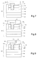
- the dielectric layer 120 is etched, by a lithographic process followed by etching, for example dry plasma etching, wet etching, or a combination of these, to form a first trench 121.
- the first trench 121 extends over the area of the wafer 100 which is arranged between the gate region 109 and the drain electrode 116, through most part of the thickness of the dielectric layer 120, but stops at a distance from the gate insulation layer 111, for example at 50 nm.
- a second trench 122 is created, with a same process, adjacent to the first trench 121.
- the second trench 122 is arranged between the first trench 121 and the vertical line passing through the drain electrode 116 and extends through the dielectric layer 120; moreover, its depth is slightly smaller than the first trench 121, for example its bottom end is arranged at 200 nm from the gate insulation layer 111.
- a plurality of trenches 123 are formed, adjacent to the second trench 122.
- the plurality of trenches 123 is arranged between the second trench 122 and the vertical line passing through the drain electrode 116 and extends through the thickness of the dielectric layer 120 so that each trench 123 is less deep than the adjacent one, moving toward the gate region 109, and deeper than the adjacent one, moving toward the drain electrode 116.
- the plurality of trenches 121-123 forms a non-connected cavity 126.
- a metal layer is deposited on the dielectric layer 120.
- the metal layer is in direct electrical contact with the source electrode 115 and drain electrode 116 where the dielectric layer 120 has been removed.
- the metal layer is defined, according to a photolithographic process, thereby forming a field plate 131 and a drain contact 134.
- the field plate 131 comprises a planar portion 125 on the dielectric layer 120 and a projecting region formed by a plurality of fingers 124 projecting inside trenches 121, 122, and 123.
- the planar portion 125 is in direct electrical contact with the source electrode 115 and forms a source contact.
- the drain contact 134 is in direct electrical contact with the drain electrode 116.
- the field plate 131 thus has, towards the wafer 100, an envelope surface or profile 133 (see in particular the enlarged detail) defined by a plurality of steps 132 having a distance, from the wafer 100, that increases moving from the gate region 109 to the drain electrode 116.
- the envelope surface 133 defines on average a surface that is sloped with respect to the surface plane of the wafer 100 and thus allows an optimization of the electrical field to be obtained and therefore a high breakdown voltage also during high-power operation, as discussed previously.
- the final wafer 100' thus obtained is thus planar and does not require further planarization steps. After dicing, a plurality of normally off HEMT devices 50 is obtained.
- the same manufacturing steps are carried out as described previously with reference to Figures 1-7 .
- the dielectric layer 120 is etched, according to the same process as the previous embodiment, in a first area 135 arranged between the vertical line passing through the gate region 109 and the vertical line passing through the drain electrode 116, forming a cavity 140.
- the dielectric layer 120 is etched for a depth smaller than in the embodiment of Figure 8 , for the reason that will be explained hereinafter.
- a second etch of the dielectric layer 120 is carried out.
- the second etch removes selective portions of the dielectric layer 120 in the first area 135 and in a second area 136, adjacent and contiguous to the first area 135, moving toward the drain electrode 116.
- a widening and deepening of the cavity 140 is obtained, and the cavity now occupies the second area 136 and, in the first area 135, has a depth caused by the first and second etches.
- one or more further etches of the dielectric layer 120 are performed in the first and second areas 135, 136 and in a plurality of areas 137, adjacent and contiguous to each other as well as to the second area 136, arranged between the second area 136 and the vertical line passing through the drain electrode 116.
- a further widening and deepening of the cavity 140 is obtained. Consequently, the cavity 140, in the first area 135, has a depth given by the sum of all the etches, in the second area 136 has a depth determined by the sum of the second and further etches and, in the plurality of areas 137, a depth that is progressively smaller.
- the cavity 140, in each further area 137 has a depth smaller than in an adjacent area moving toward the gate region 109 and a depth greater than in an adjacent area 137 moving toward the drain electrode 116.
- a single cavity 140 extends inside the dielectric layer 120; the cavity 140 is delimited, towards the wafer 100, by a staircase surface 144, the steps whereof are arranged at an increasing distance from the wafer 100 moving from the gate region 109 to the drain electrode 116.
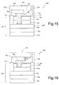
- a metal layer is deposited over the dielectric layer 120, similar to what described with reference to Figure 11 .
- the metal layer is defined, according to a photolithographic process, so as to obtain a field plate 142 and the drain contact 134.
- the field plate 142 comprises the planar portion 139 and a single projecting portion 145, the bottom surface whereof (towards the wafer 100) reproduces the shape of the cavity 140 and thus has a plurality of steps 143.
- an HEMT device 150 is obtained, which also here is of a normally off type.
- Figure 16 shows a different embodiment where the gate region 209 extends through the passivation layer 205 alone and not through the barrier layer 204, thus forming an HEMT device 250 of a normally on type.
- the field plate 131 is formed as in the first embodiment and has a plurality of projecting fingers 124 delimited by an envelope surface 133 defined by a plurality of steps 132.
- an HEMT device of a normally on type may be formed with a field plate having a single projecting portion, similar to the field plate 142 of Figure 14 , in a manner not shown.
- the HEMT device described herein and the corresponding manufacturing process are advantageous as compared to the known solutions.
- the device has high planarity following upon a single planarization operation, thus facilitating electrical connection and not requiring repeated costly planarizations.
- the manufacturing process described comprises manufacturing steps that are in per se standard in semiconductor technology and are thus reliable and easy to control.
- the field plate 131, 142 as a whole, has a profile sloped towards the wafer 100, thus ensuring the desired optimization of the electrical field and voltage strength.
- the final HEMT device thus has high reliability.
- the number of steps of the bottom surface of the field plate (defined by the bottom end of the projecting fingers 124 of Figure 11 or by the steps 132 of the single projecting portion 143 of Figure 15 ) may range from two on.
- each step of the field plate 131, 142 may vary according the design specifications, and these parameters may be optimized by the designer without any difficulty.
Landscapes
- Junction Field-Effect Transistors (AREA)
Abstract
Description
- The present invention relates to a high-power and high-frequency heterostructure field-effect transistor.
- As is known, AlGaN/GaN heterostructures have drawn high interest for manufacturing high-power and high-frequency field-effect transistors, by virtue of the high breakdown voltage of the material and the high density and mobility of carrier ions in the two-dimensional electron gas (2DEG).
- High-electron-mobility transistors (HEMTs) based on AlGaN/GaN are generally grown on a silicon substrate, since cheap substrates based of gallium nitride (GaN) are not available. Therefore, the device is horizontal and the source, drain, and gate electrodes are arranged on the upper surface of the wafer. Thus, the wafer breakdown voltage is linked both to the vertical breakdown voltage and to the lateral distance between the source and the drain electrodes.
- Although gallium nitride and its alloys are wide band-gap and high breakdown semiconductors, one of the critical aspects of HEMT power devices of gallium nitride is obtaining a good electrical field distribution during switch-off.
- Therefore, the structure of an HEMT is carefully studied in order to optimize the electrical field distribution and to allow the device to operate at a maximum switching rate, when subjected to a high voltage variation. Without an appropriate shaping of the existing electrical field, in fact, the latter may cause injection of electrons in traps, thus degrading the output current and the on-state resistance during switching. This phenomenon is frequently referred to as dynamic degradation, current drop, or DC-RF dispersion.
- To prevent this phenomenon, in microwave applications, it has been proposed to use a V-shaped gate region with an integrated slant field plate (see, e.g., Y. Dora, et al. "High Breakdown Voltage Achieved on AlGaN/GaN HEMTs With Integrated Slant Field Plates", IEEE ELECTRON DEVICE LETTERS, Vol. 27, N. 9, September 2006, pp. 713-715 and R. Chu et al. "V-Gate GaN HEMTs for X-Band Power Applications", IEEE ELECTRON DEVICE LETTERS, Vol. 29, No. 9, September 2008, pp. 974-976). For high-voltage applications, the use of a structure has also been proposed having a plurality of separate, overlying field plates, to increase the operating voltage (multiple-field-plate solution, see, e.g., H. Xing et al. "High-Breakdown Voltage AlGaN/GaN HEMTs Achieved by Multiple Field Plates", IEEE ELECTRON DEVICE LETTERS, Vol. 25, No. 4, April 2004, pp. 161-163). Another known solution (see R. Chu et al. "1200-V Normally Off GaN-on-Si Field-Effect Transistors with Low Dynamic On-Resistance", IEEE ELECTRON DEVICE LETTERS, VOL. 32, No. 5, May 2011, pp. 632-634) shows a different multiple field plate having overlying portions, in mutual electrical contact. A similar approach is described in
US 8,530,978 B1 , but with a sloped field plate connected to the source electrode. - In particular, the device described in
US 8,530,978 B1 comprises a stack of AlGaN/GaN epitaxial layers on a silicon substrate. A passivation layer of dielectric material covers the stack of epitaxial layers and accommodates source and drain electrodes, a gate electrode, a first field plate connected to the gate region, and a second field plate connected to the source electrode. The second field plate has a sloped bottom surface. The first field plate, connected to the gate region, is intended to prevent charge trapping at low voltage. - The sloped shape of the second field plate is obtained by exposing a photoresist through a greyscale mask. This mask allows to modulate the intensity of the passing light and to obtain a sloped profile in the photoresist. This profile is then transferred onto the underlying dielectric layer by dry etching. The process for forming the sloped field plate is simpler and faster than the process for forming a plurality of separate field plates since the latter requires numerous successive metal deposition and definition steps.
- The presence of a sloped field plate enables the increase of the dynamic on-state resistance at 600 V to be reduced from 47%, that may be achieved with the multiple-field-plate device, to 19%. The improvement of performance is thought to be due to a more linear profile of the electrical field, which can be achieved by virtue of the sloped field plate.
- However, also the solution with sloped field plate is not free from disadvantages. In fact, it involves a complex manufacturing process and a final planarization step. Forming the sloped field plate is thus costly and may not be sufficiently controllable.
- The aim of the present invention is to provide a different manufacturing process and a new HEMT device having a field plate with a sloped surface.
- According to the present invention, a manufacturing process and a heterostructure field-effect transistor are provided, as defined in the attached claims.
- In practice, to form the field plate, the dielectric layer overlying the gate, drain, and source regions is subjected to a plurality of successive etching steps such as to form a cavity, connected or not connected, with a bottom surface or an underside envelope having a plurality of steps, thereby meaning a plurality of discontinuous surface portions adjacent to each other, wherein each surface portion extends at a different distance from the underlying wafer with respect to adjacent surface portions.
- For a better understanding of the present invention, preferred embodiments thereof are now described, purely by way of nonlimiting example, with reference to the attached drawings, wherein:
-
Figures 1-11 are cross-sections through a semiconductor material wafer in successive manufacturing steps of a first embodiment of the present field-effect HEMT device; -
Figures 12-15 are cross-sections through a semiconductor material wafer in successive manufacturing steps of a second embodiment of the present field-effect HEMT device; and -
Figure 16 shows a cross-section of a variant of the device ofFigure 11 . -
Figure 1 shows a portion of awafer 100 for manufacturing an HEMT device, according to one embodiment of the present device. In particular, the described embodiment regards a heterostructure field-effect transistor of AlGaN/GaN. - The
wafer 100 comprises asubstrate 101 of, e.g., silicon, silicon carbide (SiC), or sapphire (Al2O3) overlaid by abuffer layer 102, for example of aluminium and gallium nitride (AlGaN) or of gallium and indium nitride (InGaN). Achannel layer 103 extends on thebuffer layer 102 and is here of intrinsic gallium nitride (GaN), having a thickness of, e.g., ca. 10 nm to ca. 10 µm. Abarrier layer 104, here of aluminium and gallium nitride (AlGaN) of an intrinsic type, extends on thechannel layer 103, in contact therewith, and has a thickness of, e.g., ca. 5 nm and ca. 400 nm. Apassivation layer 105 of dielectric material such as silicon nitride (Si3N4) or silicon oxide (SiO2) extends on thebarrier layer 104. - As shown in
Figure 2 , thepassivation layer 105 and thebarrier layer 104 are selectively removed at the portion of thewafer 100 where, in subsequent steps, a gate region of the HEMT device is to be formed. For instance, lithography, etching of thepassivation layer 105 and dry etching of thebarrier layer 104 are carried out of so as to remove selective portions thereof. Atrench 110 is thus formed, which extends throughout the thickness of thepassivation layer 105 and of thebarrier layer 104. - Next,
Figure 3 , agate insulation layer 111 is deposited, for example made of a material chosen from aluminium nitride (AlN), silicon nitride (SiN), aluminium oxide (Al2O3), or silicon oxide (SiO2). Thegate insulation layer 111 may have a thickness of between 1 and 50 nm, for example, 20 nm. - Then, as shown in
Figure 4 , aconductive layer 112 is deposited on thegate insulation layer 111 and fills thetrench 110. For instance, theconductive layer 112 is made of metal material, such as tantalum (Ta), tantalum nitride (TaN), titanium nitride (TiN), palladium (Pa), tungsten (W), tungsten silicide (WSi2), titanium aluminium (Ti/Al), or nickel gold (Ni/Au). - The
conductive layer 112 is then selectively removed (Figure 5 ), through lithographic and etching steps per se known so as to remove theconductive layer 112 from thewafer 100, except for the portion extending in thetrench 110 and for an adjacent portion, projecting from thewafer 100. A gate metallization 112' is thus formed. The gate metallization 112' and thegate insulation layer 111 form, as a whole, the gate region, designated as a whole by 109, of the HEMT device. Then, one or more further masked etching steps of thegate insulation layer 111, of thepassivation layer 105, and of thebarrier layer 104 are carried out at the areas of thewafer 100 where the source and drain electrodes of the HEMT device are to be formed. In particular,openings gate region 109 and at a distance therefrom. - Next, as shown in
Figure 6 , ohmic contacts are formed to provide the source anddrain electrodes wafer 100 and in particular inside theopenings wafer 100, except for the portions extending in theopenings drain electrode electrodes - Then,
Figure 7 , adielectric layer 120 is deposited, for example of silicon nitride or silicon oxide or TEOS (tetraethylorthosilicate)/SOG(Spin-On-Glass)/TEOS, which coats the source anddrain electrodes gate region 109, and thegate insulation layer 111. Thedielectric layer 120 thus obtained is then planarized (for example via CMP - Chemical Mechanical Polishing). Next, portions of thedielectric layer 120 are selectively removed, by a photolithographic process followed by an etch, for example a dry plasma etch, a wet etch or a combination of these, at the source anddrain electrodes - Next,
Figure 8 , thedielectric layer 120 is etched, by a lithographic process followed by etching, for example dry plasma etching, wet etching, or a combination of these, to form afirst trench 121. Thefirst trench 121 extends over the area of thewafer 100 which is arranged between thegate region 109 and thedrain electrode 116, through most part of the thickness of thedielectric layer 120, but stops at a distance from thegate insulation layer 111, for example at 50 nm. - Next,
Figure 9 , asecond trench 122 is created, with a same process, adjacent to thefirst trench 121. In particular, thesecond trench 122 is arranged between thefirst trench 121 and the vertical line passing through thedrain electrode 116 and extends through thedielectric layer 120; moreover, its depth is slightly smaller than thefirst trench 121, for example its bottom end is arranged at 200 nm from thegate insulation layer 111. - Then,
Figure 10 , using the same process as described with reference toFigures 8 and 9 , a plurality oftrenches 123 are formed, adjacent to thesecond trench 122. The plurality oftrenches 123 is arranged between thesecond trench 122 and the vertical line passing through thedrain electrode 116 and extends through the thickness of thedielectric layer 120 so that eachtrench 123 is less deep than the adjacent one, moving toward thegate region 109, and deeper than the adjacent one, moving toward thedrain electrode 116. As a whole, the plurality of trenches 121-123 forms anon-connected cavity 126. - Next,
Figure 11 , a metal layer is deposited on thedielectric layer 120. The metal layer is in direct electrical contact with thesource electrode 115 anddrain electrode 116 where thedielectric layer 120 has been removed. Then, the metal layer is defined, according to a photolithographic process, thereby forming afield plate 131 and adrain contact 134. Thefield plate 131 comprises aplanar portion 125 on thedielectric layer 120 and a projecting region formed by a plurality offingers 124 projecting insidetrenches planar portion 125 is in direct electrical contact with thesource electrode 115 and forms a source contact. Thedrain contact 134 is in direct electrical contact with thedrain electrode 116. - The
field plate 131 thus has, towards thewafer 100, an envelope surface or profile 133 (see in particular the enlarged detail) defined by a plurality ofsteps 132 having a distance, from thewafer 100, that increases moving from thegate region 109 to thedrain electrode 116. In practice, theenvelope surface 133 defines on average a surface that is sloped with respect to the surface plane of thewafer 100 and thus allows an optimization of the electrical field to be obtained and therefore a high breakdown voltage also during high-power operation, as discussed previously. - The final wafer 100' thus obtained is thus planar and does not require further planarization steps. After dicing, a plurality of normally off
HEMT devices 50 is obtained. - In a different embodiment, initially the same manufacturing steps are carried out as described previously with reference to
Figures 1-7 . Next,Figure 12 , thedielectric layer 120 is etched, according to the same process as the previous embodiment, in afirst area 135 arranged between the vertical line passing through thegate region 109 and the vertical line passing through thedrain electrode 116, forming acavity 140. - Here, the
dielectric layer 120 is etched for a depth smaller than in the embodiment ofFigure 8 , for the reason that will be explained hereinafter. - Then,
Figure 13 , a second etch of thedielectric layer 120 is carried out. In detail, the second etch removes selective portions of thedielectric layer 120 in thefirst area 135 and in asecond area 136, adjacent and contiguous to thefirst area 135, moving toward thedrain electrode 116. Thereby, a widening and deepening of thecavity 140 is obtained, and the cavity now occupies thesecond area 136 and, in thefirst area 135, has a depth caused by the first and second etches. - Next,
Figure 14 , one or more further etches of thedielectric layer 120 are performed in the first andsecond areas areas 137, adjacent and contiguous to each other as well as to thesecond area 136, arranged between thesecond area 136 and the vertical line passing through thedrain electrode 116. Thereby, a further widening and deepening of thecavity 140 is obtained. Consequently, thecavity 140, in thefirst area 135, has a depth given by the sum of all the etches, in thesecond area 136 has a depth determined by the sum of the second and further etches and, in the plurality ofareas 137, a depth that is progressively smaller. In this way, thecavity 140, in eachfurther area 137, has a depth smaller than in an adjacent area moving toward thegate region 109 and a depth greater than in anadjacent area 137 moving toward thedrain electrode 116. - At the end of the etching phase, in the embodiment of
Figures 12-15 , asingle cavity 140 extends inside thedielectric layer 120; thecavity 140 is delimited, towards thewafer 100, by astaircase surface 144, the steps whereof are arranged at an increasing distance from thewafer 100 moving from thegate region 109 to thedrain electrode 116. - Next,
Figure 15 , a metal layer is deposited over thedielectric layer 120, similar to what described with reference toFigure 11 . Then, the metal layer is defined, according to a photolithographic process, so as to obtain afield plate 142 and thedrain contact 134. Here, thefield plate 142 comprises theplanar portion 139 and a single projectingportion 145, the bottom surface whereof (towards the wafer 100) reproduces the shape of thecavity 140 and thus has a plurality ofsteps 143. - After dicing the final wafer 100', an
HEMT device 150 is obtained, which also here is of a normally off type. -
Figure 16 shows a different embodiment where thegate region 209 extends through thepassivation layer 205 alone and not through thebarrier layer 204, thus forming anHEMT device 250 of a normally on type. - In
Figure 16 , thefield plate 131 is formed as in the first embodiment and has a plurality of projectingfingers 124 delimited by anenvelope surface 133 defined by a plurality ofsteps 132. - As an alternative thereto, an HEMT device of a normally on type may be formed with a field plate having a single projecting portion, similar to the
field plate 142 ofFigure 14 , in a manner not shown. - The HEMT device described herein and the corresponding manufacturing process are advantageous as compared to the known solutions. In fact, the device has high planarity following upon a single planarization operation, thus facilitating electrical connection and not requiring repeated costly planarizations. Furthermore, the manufacturing process described comprises manufacturing steps that are in per se standard in semiconductor technology and are thus reliable and easy to control. The
field plate wafer 100, thus ensuring the desired optimization of the electrical field and voltage strength. The final HEMT device thus has high reliability. - Finally, it is clear that modifications and variations may be made to the process and to the device described and illustrated herein, without thereby departing from the scope of the present invention, as defined in the attached claims. For instance, the various embodiments described may be combined so as to provide further solutions.
- In addition, in all the solutions, the number of steps of the bottom surface of the field plate (defined by the bottom end of the projecting
fingers 124 ofFigure 11 or by thesteps 132 of the single projectingportion 143 ofFigure 15 ) may range from two on. - Furthermore, the depth, width, and mutual distance of each step of the
field plate
Claims (16)
- A process for manufacturing a heterostructure field-effect transistor (50; 150; 250), comprising the steps of:- in a wafer (100) comprising a channel layer (103) of a first semiconductor material, a barrier layer (104) of a second semiconductor material, and a passivation layer (105; 205) of dielectric material, forming a gate region (109; 209) extending through the wafer (100);- forming drain and source contacts (115, 116) extending through the wafer (100) on different sides of the gate region (109; 209);- forming a dielectric layer (120) over the gate region (109; 209) and the passivation layer (105; 205); and- removing selective portions of the dielectric layer (120) through a plurality of etches so as to form a cavity (126; 140) arranged between the gate region (109; 209) and the drain electrode (116) and having a surface (133; 144) looking toward the wafer (100), the surface being delimited by a plurality of steps (132; 143) at different distances from the wafer (100); and- filling the cavity (126; 140) with conductive material to form a field plate (131; 142) coupled to the source electrode (115) and extending over the gate region (109; 209) and inside the cavity (126; 140).
- A process according to claim 1, wherein forming a cavity (126) comprises forming a plurality of adjacent trenches (121, 122, 123) arranged at a distance from each other, and the surface is an envelope surface (133).
- A process according to claim 1, wherein forming a cavity (140) comprises carrying out a first etch of the dielectric layer (120) in a first area (135) and carrying out a second etch of the dielectric layer in the first area (135) and in a second area (136) contiguous to the first area (135) so as to form a single cavity (140), and the surface is a step-wise delimitation surface (144).
- A process according to claim 3, wherein forming a cavity (140) comprises carrying out a third etch of the dielectric layer (120) in the first area (135), in the second area (136), and in a third area (137) of the dielectric layer that is contiguous to the second area.
- A process according to any of the preceding claims, wherein forming a cavity (121, 122, 123; 140) comprises forming steps (132; 143) arranged at an increasing distance from the wafer (100) moving from the gate region (109; 209) to the drain electrode (116).
- A process according to any of the preceding claims, wherein the conductive material is metal.
- A process according to any of the preceding claims, comprising defining the conductive material and forming a planar portion (125 139) of the field plate (131; 142), as well as source and drain contacts after filling the cavity (121, 122, 123; 140).
- A heterostructure field-effect transistor (50; 150; 250), comprising:a body including a channel layer (103) of a first semiconductor material; a barrier layer (104) of a second semiconductor material, over the channel layer (103); and a passivation layer (105; 205), over the barrier layer (104);source and drain electrodes (115, 116) extending in the body (5);a gate region (109) extending in the body (5) between the source and drain electrodes (115, 116);a dielectric layer (120) over the gate region (109; 209) and over the passivation layer (105; 205); anda field plate (131; 142) of conductive material coupled to the source electrode (115) and extending inside the dielectric layer (120) in an area comprised between the gate region (109; 209) and the drain electrode (116);
the field plate (131; 142) having a surface (133; 144) facing the wafer (100) and having a plurality of steps (132; 143). - A transistor according to claim 8, wherein the steps (132; 143) have an increasing distance from the body moving from the gate region (109; 209) to the drain electrode (116).
- A transistor according to claim 8 or 9, wherein the field plate (131; 142) comprises a planar portion (125) extending over the dielectric layer (120) and a plurality of projecting fingers (124), distinct from each other and arranged at a mutual distance, the projecting fingers (124) extending from the planar portion (125) inside the dielectric layer (120) towards the body, wherein the surface is an envelope surface of the projecting portions.
- A transistor according to claim 8 or 9, wherein the field plate comprises a planar portion (139) extending over the dielectric layer (120) and a single projecting region (145) extending from the planar portion (139) towards the body and delimited at a bottom by the surface.
- A transistor according to any of claims 8-11, wherein the body comprises a trench (110), and the gate region (109; 209) comprises a gate electrode and a gate insulation layer (111), the gate region is arranged inside the trench, and the gate insulation layer extends between the passivation layer (105; 205) and the dielectric layer (120) and inside the trench (110), around the gate electrode.
- A transistor according to any of claims 8-12, wherein the gate region (109, 209) extends inside the passivation layer (105, 205).
- A transistor according to any of claims 8-12, wherein the gate region (109, 209) extends inside the passivation layer (105, 205) and the barrier region (104).
- A transistor according to any of claims 8-14, wherein the first and second semiconductor materials have different band gaps and comprise elements of Groups III-V of the Periodic Table.
- A transistor according to claim 15, wherein the channel layer (103) is of gallium nitride, and the barrier layer (104) is of aluminium and gallium nitride.
Priority Applications (6)
| Application Number | Priority Date | Filing Date | Title |
|---|---|---|---|
| EP16425048.2A EP3252824B1 (en) | 2016-05-30 | 2016-05-30 | High-power and high-frequency heterostructure field-effect transistor |
| CN201611065063.0A CN107452625B (en) | 2016-05-30 | 2016-11-28 | High power and high frequency heterojunction field effect transistor |
| CN201621285202.6U CN206412319U (en) | 2016-05-30 | 2016-11-28 | High power and high-frequency HFET |
| US15/371,012 US10050136B2 (en) | 2016-05-30 | 2016-12-06 | High-power and high-frequency heterostructure field-effect transistor |
| US16/036,597 US10411123B2 (en) | 2016-05-30 | 2018-07-16 | High-power and high-frequency heretostructure field-effect transistor |
| US16/526,915 US10651304B2 (en) | 2016-05-30 | 2019-07-30 | High-power and high-frequency heterostructure field-effect transistor |
Applications Claiming Priority (1)
| Application Number | Priority Date | Filing Date | Title |
|---|---|---|---|
| EP16425048.2A EP3252824B1 (en) | 2016-05-30 | 2016-05-30 | High-power and high-frequency heterostructure field-effect transistor |
Publications (2)
| Publication Number | Publication Date |
|---|---|
| EP3252824A1 true EP3252824A1 (en) | 2017-12-06 |
| EP3252824B1 EP3252824B1 (en) | 2021-10-20 |
Family
ID=56787399
Family Applications (1)
| Application Number | Title | Priority Date | Filing Date |
|---|---|---|---|
| EP16425048.2A Active EP3252824B1 (en) | 2016-05-30 | 2016-05-30 | High-power and high-frequency heterostructure field-effect transistor |
Country Status (3)
| Country | Link |
|---|---|
| US (3) | US10050136B2 (en) |
| EP (1) | EP3252824B1 (en) |
| CN (2) | CN206412319U (en) |
Families Citing this family (19)
| Publication number | Priority date | Publication date | Assignee | Title |
|---|---|---|---|---|
| EP3252824B1 (en) * | 2016-05-30 | 2021-10-20 | STMicroelectronics S.r.l. | High-power and high-frequency heterostructure field-effect transistor |
| US10204791B1 (en) * | 2017-09-22 | 2019-02-12 | Power Integrations, Inc. | Contact plug for high-voltage devices |
| CN109727862B (en) * | 2018-12-30 | 2020-06-16 | 苏州汉骅半导体有限公司 | Semiconductor device and method for manufacturing the same |
| US11127846B2 (en) | 2019-07-12 | 2021-09-21 | Vanguard International Semiconductor Corporation | High electron mobility transistor devices and methods for forming the same |
| US12334392B2 (en) * | 2019-08-07 | 2025-06-17 | Intel Corporation | Multi-height interconnect trenches for resistance and capacitance optimization |
| US11476154B2 (en) * | 2019-09-26 | 2022-10-18 | Raytheon Company | Field effect transistor having improved gate structures |
| CN113130641A (en) * | 2020-01-15 | 2021-07-16 | 世界先进积体电路股份有限公司 | Semiconductor device and method of forming the same |
| US11695068B2 (en) | 2020-03-09 | 2023-07-04 | Insyt, Inc. | Greyscale lithography for double-slanted gate connected field plate |
| US12400858B2 (en) | 2020-03-09 | 2025-08-26 | Insyt, Inc. | Greyscale lithography techniques for manufacturing field plates |
| US11152474B1 (en) * | 2020-04-21 | 2021-10-19 | Vanguard International Semiconductor Corporation | Semiconductor device and method for forming the same |
| CN111863950B (en) * | 2020-07-28 | 2021-08-20 | 西安电子科技大学 | Junction Gate-Drain Power Devices |
| CN114649409A (en) * | 2020-12-18 | 2022-06-21 | 华为技术有限公司 | High electron mobility transistor, preparation method and power amplifier/switch |
| CN114823888B (en) | 2021-01-22 | 2025-10-03 | 联华电子股份有限公司 | High electron mobility transistor and manufacturing method thereof |
| CN114864683A (en) * | 2021-02-04 | 2022-08-05 | 联华电子股份有限公司 | Semiconductor device and method for fabricating the same |
| KR102916033B1 (en) * | 2021-04-06 | 2026-01-20 | 삼성전자주식회사 | Power device and method of manufacturing the same |
| CN113519064B (en) * | 2021-06-02 | 2023-03-17 | 英诺赛科(苏州)科技有限公司 | Nitrogen-based semiconductor device and method for manufacturing the same |
| CN113809160A (en) * | 2021-08-25 | 2021-12-17 | 西安电子科技大学 | Gold-free field plate GaN-based radio frequency device and manufacturing method thereof |
| CN117727775A (en) * | 2024-02-08 | 2024-03-19 | 深圳天狼芯半导体有限公司 | GaN HEMT with comb-shaped source electrode field plate for improving withstand voltage and preparation method |
| CN121568420B (en) * | 2026-01-19 | 2026-03-31 | 安建科技(深圳)有限公司 | Power semiconductor devices with integrated field plate structure and their manufacturing method |
Citations (4)
| Publication number | Priority date | Publication date | Assignee | Title |
|---|---|---|---|---|
| CN102903762A (en) * | 2012-10-22 | 2013-01-30 | 苏州英能电子科技有限公司 | Schottky diode and preparation method thereof |
| US8530978B1 (en) | 2011-12-06 | 2013-09-10 | Hrl Laboratories, Llc | High current high voltage GaN field effect transistors and method of fabricating same |
| US20140264431A1 (en) * | 2013-03-13 | 2014-09-18 | Transphorm Inc. | Enhancement-mode iii-nitride devices |
| US9257513B1 (en) * | 2014-08-05 | 2016-02-09 | Semiconductor Components Industries, Llc | Semiconductor component and method |
Family Cites Families (6)
| Publication number | Priority date | Publication date | Assignee | Title |
|---|---|---|---|---|
| DE102009018054B4 (en) * | 2009-04-21 | 2018-11-29 | Infineon Technologies Austria Ag | Lateral HEMT and method of making a lateral HEMT |
| JP2014072379A (en) * | 2012-09-28 | 2014-04-21 | Fujitsu Ltd | Compound semiconductor device and manufacturing method of the same |
| JP6522521B2 (en) * | 2013-02-15 | 2019-05-29 | トランスフォーム インコーポレーテッド | Electrode of semiconductor device and method of manufacturing the same |
| CN103579332B (en) * | 2013-10-31 | 2016-04-13 | 中航(重庆)微电子有限公司 | Hetero junction field effect pipe and preparation method thereof |
| CN103779406B (en) * | 2014-01-20 | 2016-05-04 | 西安电子科技大学 | Add source field plate depletion type insulated gate AlGaN/GaN device architecture and preparation method thereof |
| EP3252824B1 (en) * | 2016-05-30 | 2021-10-20 | STMicroelectronics S.r.l. | High-power and high-frequency heterostructure field-effect transistor |
-
2016
- 2016-05-30 EP EP16425048.2A patent/EP3252824B1/en active Active
- 2016-11-28 CN CN201621285202.6U patent/CN206412319U/en active Active
- 2016-11-28 CN CN201611065063.0A patent/CN107452625B/en active Active
- 2016-12-06 US US15/371,012 patent/US10050136B2/en active Active
-
2018
- 2018-07-16 US US16/036,597 patent/US10411123B2/en active Active
-
2019
- 2019-07-30 US US16/526,915 patent/US10651304B2/en active Active
Patent Citations (4)
| Publication number | Priority date | Publication date | Assignee | Title |
|---|---|---|---|---|
| US8530978B1 (en) | 2011-12-06 | 2013-09-10 | Hrl Laboratories, Llc | High current high voltage GaN field effect transistors and method of fabricating same |
| CN102903762A (en) * | 2012-10-22 | 2013-01-30 | 苏州英能电子科技有限公司 | Schottky diode and preparation method thereof |
| US20140264431A1 (en) * | 2013-03-13 | 2014-09-18 | Transphorm Inc. | Enhancement-mode iii-nitride devices |
| US9257513B1 (en) * | 2014-08-05 | 2016-02-09 | Semiconductor Components Industries, Llc | Semiconductor component and method |
Non-Patent Citations (5)
| Title |
|---|
| H. XING ET AL.: "High-Breakdown Voltage AlGaN/GaN HEMTs Achieved by Multiple Field Plates", IEEE ELECTRON DEVICE LETTERS, vol. 25, no. 4, April 2004 (2004-04-01), pages 161 - 163, XP001190361, DOI: doi:10.1109/LED.2004.824845 |
| R. CHU ET AL.: "1200-V Normally Off GaN-on-Si Field-Effect Transistors with Low Dynamic On-Resistance", IEEE ELECTRON DEVICE LETTERS, vol. 32, no. 5, May 2011 (2011-05-01), pages 632 - 634, XP011479570, DOI: doi:10.1109/LED.2011.2118190 |
| R. CHU ET AL.: "V-Gate GaN HEMTs for X-Band Power Applications", IEEE ELECTRON DEVICE LETTERS, vol. 29, no. 9, September 2008 (2008-09-01), pages 974 - 976, XP011233563, DOI: doi:10.1109/LED.2008.2001639 |
| RONGMING CHU ET AL: "1200-V Normally Off GaN-on-Si Field-Effect Transistors With Low Dynamic on -Resistance", IEEE ELECTRON DEVICE LETTERS, IEEE SERVICE CENTER, NEW YORK, NY, US, vol. 32, no. 5, 1 May 2011 (2011-05-01), pages 632 - 634, XP011479570, ISSN: 0741-3106, DOI: 10.1109/LED.2011.2118190 * |
| Y. DORA ET AL.: "High Breakdown Voltage Achieved on AlGaN/GaN HEMTs With Integrated Slant Field Plates", IEEE ELECTRON DEVICE LETTERS, vol. 27, no. 9, September 2006 (2006-09-01), pages 713 - 715, XP001546725, DOI: doi:10.1109/LED.2006.881020 |
Also Published As
| Publication number | Publication date |
|---|---|
| US10411123B2 (en) | 2019-09-10 |
| CN206412319U (en) | 2017-08-15 |
| CN107452625B (en) | 2021-02-19 |
| US20180342606A1 (en) | 2018-11-29 |
| US20170345918A1 (en) | 2017-11-30 |
| EP3252824B1 (en) | 2021-10-20 |
| CN107452625A (en) | 2017-12-08 |
| US10050136B2 (en) | 2018-08-14 |
| US10651304B2 (en) | 2020-05-12 |
| US20190355842A1 (en) | 2019-11-21 |
Similar Documents
| Publication | Publication Date | Title |
|---|---|---|
| US10651304B2 (en) | High-power and high-frequency heterostructure field-effect transistor | |
| US12148823B2 (en) | Double-channel HEMT device and manufacturing method thereof | |
| TWI600155B (en) | Electrode for a semiconductor device and method of forming the same | |
| CN104332498B (en) | A kind of tiltedly preparation method of field plate power device and oblique field plate power device | |
| CN104576742B (en) | III N devices and forming method thereof | |
| CN110233103A (en) | High electron mobility transistor with deep carrier gas contact structures | |
| US10985253B2 (en) | Semiconductor devices with multiple channels and three-dimensional electrodes | |
| CN114144891B (en) | Nitride-based semiconductor device and method of manufacturing the same | |
| CN110233104A (en) | High electron mobility transistor with double thickness barrier layers | |
| US11742419B2 (en) | Cap structure coupled to source to reduce saturation current in HEMT device | |
| CN114823888A (en) | High electron mobility transistor and manufacturing method thereof | |
| KR20220015997A (en) | Gallium nitride-based device with step-wise field plate and method making the same | |
| CN114144892B (en) | Nitride-based semiconductor device and method of manufacturing the same | |
| KR101750158B1 (en) | Hemt-compatible lateral rectifier structure | |
| US12336233B2 (en) | GaN-based semiconductor device with reduced leakage current and method for manufacturing the same | |
| KR20140141126A (en) | nitride-based transistor having field relief part and method of fabricating the same | |
| CN119947165A (en) | High electron mobility transistor with regenerative barrier | |
| CN116741824A (en) | Semiconductor components and methods of forming the same | |
| CN120417454A (en) | Device with inner and outer spacers | |
| CN113906571A (en) | Semiconductor device and method for manufacturing the same | |
| CN118472016A (en) | Terminal structure for improving off-state electrical characteristics of power electronic device and preparation method thereof |
Legal Events
| Date | Code | Title | Description |
|---|---|---|---|
| PUAI | Public reference made under article 153(3) epc to a published international application that has entered the european phase |
Free format text: ORIGINAL CODE: 0009012 |
|
| STAA | Information on the status of an ep patent application or granted ep patent |
Free format text: STATUS: THE APPLICATION HAS BEEN PUBLISHED |
|
| AK | Designated contracting states |
Kind code of ref document: A1 Designated state(s): AL AT BE BG CH CY CZ DE DK EE ES FI FR GB GR HR HU IE IS IT LI LT LU LV MC MK MT NL NO PL PT RO RS SE SI SK SM TR |
|
| AX | Request for extension of the european patent |
Extension state: BA ME |
|
| STAA | Information on the status of an ep patent application or granted ep patent |
Free format text: STATUS: REQUEST FOR EXAMINATION WAS MADE |
|
| 17P | Request for examination filed |
Effective date: 20180606 |
|
| RBV | Designated contracting states (corrected) |
Designated state(s): AL AT BE BG CH CY CZ DE DK EE ES FI FR GB GR HR HU IE IS IT LI LT LU LV MC MK MT NL NO PL PT RO RS SE SI SK SM TR |
|
| GRAP | Despatch of communication of intention to grant a patent |
Free format text: ORIGINAL CODE: EPIDOSNIGR1 |
|
| STAA | Information on the status of an ep patent application or granted ep patent |
Free format text: STATUS: GRANT OF PATENT IS INTENDED |
|
| GRAJ | Information related to disapproval of communication of intention to grant by the applicant or resumption of examination proceedings by the epo deleted |
Free format text: ORIGINAL CODE: EPIDOSDIGR1 |
|
| STAA | Information on the status of an ep patent application or granted ep patent |
Free format text: STATUS: REQUEST FOR EXAMINATION WAS MADE |
|
| INTG | Intention to grant announced |
Effective date: 20210412 |
|
| RIC1 | Information provided on ipc code assigned before grant |
Ipc: H01L 29/778 20060101ALI20210326BHEP Ipc: H01L 29/66 20060101ALI20210326BHEP Ipc: H01L 29/423 20060101ALI20210326BHEP Ipc: H01L 29/417 20060101ALI20210326BHEP Ipc: H01L 29/20 20060101ALI20210326BHEP Ipc: H01L 29/40 20060101AFI20210326BHEP |
|
| RIN1 | Information on inventor provided before grant (corrected) |
Inventor name: IUCOLANO, FERDINANDO |
|
| GRAP | Despatch of communication of intention to grant a patent |
Free format text: ORIGINAL CODE: EPIDOSNIGR1 |
|
| STAA | Information on the status of an ep patent application or granted ep patent |
Free format text: STATUS: GRANT OF PATENT IS INTENDED |
|
| INTC | Intention to grant announced (deleted) | ||
| INTG | Intention to grant announced |
Effective date: 20210512 |
|
| GRAS | Grant fee paid |
Free format text: ORIGINAL CODE: EPIDOSNIGR3 |
|
| GRAA | (expected) grant |
Free format text: ORIGINAL CODE: 0009210 |
|
| STAA | Information on the status of an ep patent application or granted ep patent |
Free format text: STATUS: THE PATENT HAS BEEN GRANTED |
|
| AK | Designated contracting states |
Kind code of ref document: B1 Designated state(s): AL AT BE BG CH CY CZ DE DK EE ES FI FR GB GR HR HU IE IS IT LI LT LU LV MC MK MT NL NO PL PT RO RS SE SI SK SM TR |
|
| REG | Reference to a national code |
Ref country code: GB Ref legal event code: FG4D |
|
| REG | Reference to a national code |
Ref country code: CH Ref legal event code: EP |
|
| REG | Reference to a national code |
Ref country code: IE Ref legal event code: FG4D |
|
| REG | Reference to a national code |
Ref country code: DE Ref legal event code: R096 Ref document number: 602016065073 Country of ref document: DE |
|
| REG | Reference to a national code |
Ref country code: AT Ref legal event code: REF Ref document number: 1440635 Country of ref document: AT Kind code of ref document: T Effective date: 20211115 |
|
| REG | Reference to a national code |
Ref country code: LT Ref legal event code: MG9D |
|
| REG | Reference to a national code |
Ref country code: NL Ref legal event code: MP Effective date: 20211020 |
|
| REG | Reference to a national code |
Ref country code: AT Ref legal event code: MK05 Ref document number: 1440635 Country of ref document: AT Kind code of ref document: T Effective date: 20211020 |
|
| PG25 | Lapsed in a contracting state [announced via postgrant information from national office to epo] |
Ref country code: RS Free format text: LAPSE BECAUSE OF FAILURE TO SUBMIT A TRANSLATION OF THE DESCRIPTION OR TO PAY THE FEE WITHIN THE PRESCRIBED TIME-LIMIT Effective date: 20211020 Ref country code: LT Free format text: LAPSE BECAUSE OF FAILURE TO SUBMIT A TRANSLATION OF THE DESCRIPTION OR TO PAY THE FEE WITHIN THE PRESCRIBED TIME-LIMIT Effective date: 20211020 Ref country code: FI Free format text: LAPSE BECAUSE OF FAILURE TO SUBMIT A TRANSLATION OF THE DESCRIPTION OR TO PAY THE FEE WITHIN THE PRESCRIBED TIME-LIMIT Effective date: 20211020 Ref country code: BG Free format text: LAPSE BECAUSE OF FAILURE TO SUBMIT A TRANSLATION OF THE DESCRIPTION OR TO PAY THE FEE WITHIN THE PRESCRIBED TIME-LIMIT Effective date: 20220120 Ref country code: AT Free format text: LAPSE BECAUSE OF FAILURE TO SUBMIT A TRANSLATION OF THE DESCRIPTION OR TO PAY THE FEE WITHIN THE PRESCRIBED TIME-LIMIT Effective date: 20211020 |
|
| PG25 | Lapsed in a contracting state [announced via postgrant information from national office to epo] |
Ref country code: IS Free format text: LAPSE BECAUSE OF FAILURE TO SUBMIT A TRANSLATION OF THE DESCRIPTION OR TO PAY THE FEE WITHIN THE PRESCRIBED TIME-LIMIT Effective date: 20220220 Ref country code: SE Free format text: LAPSE BECAUSE OF FAILURE TO SUBMIT A TRANSLATION OF THE DESCRIPTION OR TO PAY THE FEE WITHIN THE PRESCRIBED TIME-LIMIT Effective date: 20211020 Ref country code: PT Free format text: LAPSE BECAUSE OF FAILURE TO SUBMIT A TRANSLATION OF THE DESCRIPTION OR TO PAY THE FEE WITHIN THE PRESCRIBED TIME-LIMIT Effective date: 20220221 Ref country code: PL Free format text: LAPSE BECAUSE OF FAILURE TO SUBMIT A TRANSLATION OF THE DESCRIPTION OR TO PAY THE FEE WITHIN THE PRESCRIBED TIME-LIMIT Effective date: 20211020 Ref country code: NO Free format text: LAPSE BECAUSE OF FAILURE TO SUBMIT A TRANSLATION OF THE DESCRIPTION OR TO PAY THE FEE WITHIN THE PRESCRIBED TIME-LIMIT Effective date: 20220120 Ref country code: NL Free format text: LAPSE BECAUSE OF FAILURE TO SUBMIT A TRANSLATION OF THE DESCRIPTION OR TO PAY THE FEE WITHIN THE PRESCRIBED TIME-LIMIT Effective date: 20211020 Ref country code: LV Free format text: LAPSE BECAUSE OF FAILURE TO SUBMIT A TRANSLATION OF THE DESCRIPTION OR TO PAY THE FEE WITHIN THE PRESCRIBED TIME-LIMIT Effective date: 20211020 Ref country code: HR Free format text: LAPSE BECAUSE OF FAILURE TO SUBMIT A TRANSLATION OF THE DESCRIPTION OR TO PAY THE FEE WITHIN THE PRESCRIBED TIME-LIMIT Effective date: 20211020 Ref country code: GR Free format text: LAPSE BECAUSE OF FAILURE TO SUBMIT A TRANSLATION OF THE DESCRIPTION OR TO PAY THE FEE WITHIN THE PRESCRIBED TIME-LIMIT Effective date: 20220121 Ref country code: ES Free format text: LAPSE BECAUSE OF FAILURE TO SUBMIT A TRANSLATION OF THE DESCRIPTION OR TO PAY THE FEE WITHIN THE PRESCRIBED TIME-LIMIT Effective date: 20211020 |
|
| REG | Reference to a national code |
Ref country code: DE Ref legal event code: R097 Ref document number: 602016065073 Country of ref document: DE |
|
| PG25 | Lapsed in a contracting state [announced via postgrant information from national office to epo] |
Ref country code: SM Free format text: LAPSE BECAUSE OF FAILURE TO SUBMIT A TRANSLATION OF THE DESCRIPTION OR TO PAY THE FEE WITHIN THE PRESCRIBED TIME-LIMIT Effective date: 20211020 Ref country code: SK Free format text: LAPSE BECAUSE OF FAILURE TO SUBMIT A TRANSLATION OF THE DESCRIPTION OR TO PAY THE FEE WITHIN THE PRESCRIBED TIME-LIMIT Effective date: 20211020 Ref country code: RO Free format text: LAPSE BECAUSE OF FAILURE TO SUBMIT A TRANSLATION OF THE DESCRIPTION OR TO PAY THE FEE WITHIN THE PRESCRIBED TIME-LIMIT Effective date: 20211020 Ref country code: EE Free format text: LAPSE BECAUSE OF FAILURE TO SUBMIT A TRANSLATION OF THE DESCRIPTION OR TO PAY THE FEE WITHIN THE PRESCRIBED TIME-LIMIT Effective date: 20211020 Ref country code: DK Free format text: LAPSE BECAUSE OF FAILURE TO SUBMIT A TRANSLATION OF THE DESCRIPTION OR TO PAY THE FEE WITHIN THE PRESCRIBED TIME-LIMIT Effective date: 20211020 Ref country code: CZ Free format text: LAPSE BECAUSE OF FAILURE TO SUBMIT A TRANSLATION OF THE DESCRIPTION OR TO PAY THE FEE WITHIN THE PRESCRIBED TIME-LIMIT Effective date: 20211020 |
|
| PLBE | No opposition filed within time limit |
Free format text: ORIGINAL CODE: 0009261 |
|
| STAA | Information on the status of an ep patent application or granted ep patent |
Free format text: STATUS: NO OPPOSITION FILED WITHIN TIME LIMIT |
|
| 26N | No opposition filed |
Effective date: 20220721 |
|
| PG25 | Lapsed in a contracting state [announced via postgrant information from national office to epo] |
Ref country code: AL Free format text: LAPSE BECAUSE OF FAILURE TO SUBMIT A TRANSLATION OF THE DESCRIPTION OR TO PAY THE FEE WITHIN THE PRESCRIBED TIME-LIMIT Effective date: 20211020 |
|
| PG25 | Lapsed in a contracting state [announced via postgrant information from national office to epo] |
Ref country code: SI Free format text: LAPSE BECAUSE OF FAILURE TO SUBMIT A TRANSLATION OF THE DESCRIPTION OR TO PAY THE FEE WITHIN THE PRESCRIBED TIME-LIMIT Effective date: 20211020 |
|
| REG | Reference to a national code |
Ref country code: CH Ref legal event code: PL |
|
| REG | Reference to a national code |
Ref country code: BE Ref legal event code: MM Effective date: 20220531 |
|
| GBPC | Gb: european patent ceased through non-payment of renewal fee |
Effective date: 20220530 |
|
| PG25 | Lapsed in a contracting state [announced via postgrant information from national office to epo] |
Ref country code: MC Free format text: LAPSE BECAUSE OF FAILURE TO SUBMIT A TRANSLATION OF THE DESCRIPTION OR TO PAY THE FEE WITHIN THE PRESCRIBED TIME-LIMIT Effective date: 20211020 Ref country code: LU Free format text: LAPSE BECAUSE OF NON-PAYMENT OF DUE FEES Effective date: 20220530 Ref country code: LI Free format text: LAPSE BECAUSE OF NON-PAYMENT OF DUE FEES Effective date: 20220531 Ref country code: CH Free format text: LAPSE BECAUSE OF NON-PAYMENT OF DUE FEES Effective date: 20220531 |
|
| PG25 | Lapsed in a contracting state [announced via postgrant information from national office to epo] |
Ref country code: IE Free format text: LAPSE BECAUSE OF NON-PAYMENT OF DUE FEES Effective date: 20220530 Ref country code: FR Free format text: LAPSE BECAUSE OF NON-PAYMENT OF DUE FEES Effective date: 20220531 |
|
| PG25 | Lapsed in a contracting state [announced via postgrant information from national office to epo] |
Ref country code: IT Free format text: LAPSE BECAUSE OF FAILURE TO SUBMIT A TRANSLATION OF THE DESCRIPTION OR TO PAY THE FEE WITHIN THE PRESCRIBED TIME-LIMIT Effective date: 20211020 Ref country code: GB Free format text: LAPSE BECAUSE OF NON-PAYMENT OF DUE FEES Effective date: 20220530 Ref country code: BE Free format text: LAPSE BECAUSE OF NON-PAYMENT OF DUE FEES Effective date: 20220531 |
|
| PG25 | Lapsed in a contracting state [announced via postgrant information from national office to epo] |
Ref country code: HU Free format text: LAPSE BECAUSE OF FAILURE TO SUBMIT A TRANSLATION OF THE DESCRIPTION OR TO PAY THE FEE WITHIN THE PRESCRIBED TIME-LIMIT; INVALID AB INITIO Effective date: 20160530 |
|
| PG25 | Lapsed in a contracting state [announced via postgrant information from national office to epo] |
Ref country code: MK Free format text: LAPSE BECAUSE OF FAILURE TO SUBMIT A TRANSLATION OF THE DESCRIPTION OR TO PAY THE FEE WITHIN THE PRESCRIBED TIME-LIMIT Effective date: 20211020 Ref country code: CY Free format text: LAPSE BECAUSE OF FAILURE TO SUBMIT A TRANSLATION OF THE DESCRIPTION OR TO PAY THE FEE WITHIN THE PRESCRIBED TIME-LIMIT Effective date: 20211020 |
|
| PG25 | Lapsed in a contracting state [announced via postgrant information from national office to epo] |
Ref country code: MT Free format text: LAPSE BECAUSE OF FAILURE TO SUBMIT A TRANSLATION OF THE DESCRIPTION OR TO PAY THE FEE WITHIN THE PRESCRIBED TIME-LIMIT Effective date: 20211020 |
|
| REG | Reference to a national code |
Ref country code: DE Ref legal event code: R079 Ref document number: 602016065073 Country of ref document: DE Free format text: PREVIOUS MAIN CLASS: H01L0029400000 Ipc: H10D0064000000 |
|
| PGFP | Annual fee paid to national office [announced via postgrant information from national office to epo] |
Ref country code: DE Payment date: 20250423 Year of fee payment: 10 |
|
| PG25 | Lapsed in a contracting state [announced via postgrant information from national office to epo] |
Ref country code: TR Free format text: LAPSE BECAUSE OF FAILURE TO SUBMIT A TRANSLATION OF THE DESCRIPTION OR TO PAY THE FEE WITHIN THE PRESCRIBED TIME-LIMIT Effective date: 20211020 |