EP3252581A1 - Integrator circuit and signal processing module - Google Patents
Integrator circuit and signal processing module Download PDFInfo
- Publication number
- EP3252581A1 EP3252581A1 EP16889664.5A EP16889664A EP3252581A1 EP 3252581 A1 EP3252581 A1 EP 3252581A1 EP 16889664 A EP16889664 A EP 16889664A EP 3252581 A1 EP3252581 A1 EP 3252581A1
- Authority
- EP
- European Patent Office
- Prior art keywords
- capacitor
- module
- integrating
- coupled
- adjustable
- Prior art date
- Legal status (The legal status is an assumption and is not a legal conclusion. Google has not performed a legal analysis and makes no representation as to the accuracy of the status listed.)
- Withdrawn
Links
Images








Classifications
-
- H—ELECTRICITY
- H03—ELECTRONIC CIRCUITRY
- H03H—IMPEDANCE NETWORKS, e.g. RESONANT CIRCUITS; RESONATORS
- H03H19/00—Networks using time-varying elements, e.g. N-path filters
- H03H19/004—Switched capacitor networks
-
- H—ELECTRICITY
- H03—ELECTRONIC CIRCUITRY
- H03M—CODING; DECODING; CODE CONVERSION IN GENERAL
- H03M1/00—Analogue/digital conversion; Digital/analogue conversion
- H03M1/12—Analogue/digital converters
- H03M1/50—Analogue/digital converters with intermediate conversion to time interval
- H03M1/52—Input signal integrated with linear return to datum
-
- G—PHYSICS
- G06—COMPUTING OR CALCULATING; COUNTING
- G06G—ANALOGUE COMPUTERS
- G06G7/00—Devices in which the computing operation is performed by varying electric or magnetic quantities
- G06G7/12—Arrangements for performing computing operations, e.g. operational amplifiers specially adapted therefor
- G06G7/18—Arrangements for performing computing operations, e.g. operational amplifiers specially adapted therefor for integration or differentiation; for forming integrals
-
- G—PHYSICS
- G06—COMPUTING OR CALCULATING; COUNTING
- G06F—ELECTRIC DIGITAL DATA PROCESSING
- G06F17/00—Digital computing or data processing equipment or methods, specially adapted for specific functions
- G06F17/10—Complex mathematical operations
- G06F17/11—Complex mathematical operations for solving equations, e.g. nonlinear equations, general mathematical optimization problems
- G06F17/12—Simultaneous equations, e.g. systems of linear equations
-
- G—PHYSICS
- G06—COMPUTING OR CALCULATING; COUNTING
- G06F—ELECTRIC DIGITAL DATA PROCESSING
- G06F3/00—Input arrangements for transferring data to be processed into a form capable of being handled by the computer; Output arrangements for transferring data from processing unit to output unit, e.g. interface arrangements
- G06F3/01—Input arrangements or combined input and output arrangements for interaction between user and computer
- G06F3/03—Arrangements for converting the position or the displacement of a member into a coded form
- G06F3/041—Digitisers, e.g. for touch screens or touch pads, characterised by the transducing means
- G06F3/0416—Control or interface arrangements specially adapted for digitisers
- G06F3/0418—Control or interface arrangements specially adapted for digitisers for error correction or compensation, e.g. based on parallax, calibration or alignment
-
- G—PHYSICS
- G06—COMPUTING OR CALCULATING; COUNTING
- G06F—ELECTRIC DIGITAL DATA PROCESSING
- G06F3/00—Input arrangements for transferring data to be processed into a form capable of being handled by the computer; Output arrangements for transferring data from processing unit to output unit, e.g. interface arrangements
- G06F3/01—Input arrangements or combined input and output arrangements for interaction between user and computer
- G06F3/03—Arrangements for converting the position or the displacement of a member into a coded form
- G06F3/041—Digitisers, e.g. for touch screens or touch pads, characterised by the transducing means
- G06F3/0416—Control or interface arrangements specially adapted for digitisers
- G06F3/0418—Control or interface arrangements specially adapted for digitisers for error correction or compensation, e.g. based on parallax, calibration or alignment
- G06F3/04182—Filtering of noise external to the device and not generated by digitiser components
-
- H—ELECTRICITY
- H03—ELECTRONIC CIRCUITRY
- H03D—DEMODULATION OR TRANSFERENCE OF MODULATION FROM ONE CARRIER TO ANOTHER
- H03D7/00—Transference of modulation from one carrier to another, e.g. frequency-changing
- H03D7/14—Balanced arrangements
-
- H—ELECTRICITY
- H03—ELECTRONIC CIRCUITRY
- H03F—AMPLIFIERS
- H03F3/00—Amplifiers with only discharge tubes or only semiconductor devices as amplifying elements
- H03F3/45—Differential amplifiers
- H03F3/45071—Differential amplifiers with semiconductor devices only
- H03F3/45076—Differential amplifiers with semiconductor devices only characterised by the way of implementation of the active amplifying circuit in the differential amplifier
- H03F3/45475—Differential amplifiers with semiconductor devices only characterised by the way of implementation of the active amplifying circuit in the differential amplifier using IC blocks as the active amplifying circuit
-
- H—ELECTRICITY
- H03—ELECTRONIC CIRCUITRY
- H03H—IMPEDANCE NETWORKS, e.g. RESONANT CIRCUITS; RESONATORS
- H03H11/00—Networks using active elements
- H03H11/02—Multiple-port networks
- H03H11/04—Frequency selective two-port networks
- H03H11/12—Frequency selective two-port networks using amplifiers with feedback
- H03H11/126—Frequency selective two-port networks using amplifiers with feedback using a single operational amplifier
-
- H—ELECTRICITY
- H03—ELECTRONIC CIRCUITRY
- H03H—IMPEDANCE NETWORKS, e.g. RESONANT CIRCUITS; RESONATORS
- H03H7/00—Multiple-port networks comprising only passive electrical elements as network components
- H03H7/38—Impedance-matching networks
-
- H—ELECTRICITY
- H03—ELECTRONIC CIRCUITRY
- H03K—PULSE TECHNIQUE
- H03K5/00—Manipulating of pulses not covered by one of the other main groups of this subclass
- H03K5/01—Shaping pulses
- H03K5/02—Shaping pulses by amplifying
-
- H—ELECTRICITY
- H03—ELECTRONIC CIRCUITRY
- H03K—PULSE TECHNIQUE
- H03K5/00—Manipulating of pulses not covered by one of the other main groups of this subclass
- H03K5/125—Discriminating pulses
- H03K5/1252—Suppression or limitation of noise or interference
-
- G—PHYSICS
- G06—COMPUTING OR CALCULATING; COUNTING
- G06F—ELECTRIC DIGITAL DATA PROCESSING
- G06F3/00—Input arrangements for transferring data to be processed into a form capable of being handled by the computer; Output arrangements for transferring data from processing unit to output unit, e.g. interface arrangements
- G06F3/01—Input arrangements or combined input and output arrangements for interaction between user and computer
- G06F3/03—Arrangements for converting the position or the displacement of a member into a coded form
- G06F3/041—Digitisers, e.g. for touch screens or touch pads, characterised by the transducing means
- G06F3/044—Digitisers, e.g. for touch screens or touch pads, characterised by the transducing means by capacitive means
-
- H—ELECTRICITY
- H03—ELECTRONIC CIRCUITRY
- H03D—DEMODULATION OR TRANSFERENCE OF MODULATION FROM ONE CARRIER TO ANOTHER
- H03D2200/00—Indexing scheme relating to details of demodulation or transference of modulation from one carrier to another covered by H03D
- H03D2200/0041—Functional aspects of demodulators
- H03D2200/0086—Reduction or prevention of harmonic frequencies
-
- H—ELECTRICITY
- H03—ELECTRONIC CIRCUITRY
- H03F—AMPLIFIERS
- H03F2200/00—Indexing scheme relating to amplifiers
- H03F2200/264—An operational amplifier based integrator or transistor based integrator being used in an amplifying circuit
-
- H—ELECTRICITY
- H03—ELECTRONIC CIRCUITRY
- H03F—AMPLIFIERS
- H03F2203/00—Indexing scheme relating to amplifiers with only discharge tubes or only semiconductor devices as amplifying elements covered by H03F3/00
- H03F2203/45—Indexing scheme relating to differential amplifiers
- H03F2203/45526—Indexing scheme relating to differential amplifiers the FBC comprising a resistor-capacitor combination and being coupled between the LC and the IC
-
- H—ELECTRICITY
- H03—ELECTRONIC CIRCUITRY
- H03F—AMPLIFIERS
- H03F2203/00—Indexing scheme relating to amplifiers with only discharge tubes or only semiconductor devices as amplifying elements covered by H03F3/00
- H03F2203/45—Indexing scheme relating to differential amplifiers
- H03F2203/45594—Indexing scheme relating to differential amplifiers the IC comprising one or more resistors, which are not biasing resistor
-
- H—ELECTRICITY
- H03—ELECTRONIC CIRCUITRY
- H03F—AMPLIFIERS
- H03F2203/00—Indexing scheme relating to amplifiers with only discharge tubes or only semiconductor devices as amplifying elements covered by H03F3/00
- H03F2203/45—Indexing scheme relating to differential amplifiers
- H03F2203/45616—Indexing scheme relating to differential amplifiers the IC comprising more than one switch, which are not cross coupled
-
- H—ELECTRICITY
- H03—ELECTRONIC CIRCUITRY
- H03H—IMPEDANCE NETWORKS, e.g. RESONANT CIRCUITS; RESONATORS
- H03H2210/00—Indexing scheme relating to details of tunable filters
- H03H2210/02—Variable filter component
- H03H2210/028—Resistor
-
- H—ELECTRICITY
- H03—ELECTRONIC CIRCUITRY
- H03H—IMPEDANCE NETWORKS, e.g. RESONANT CIRCUITS; RESONATORS
- H03H2210/00—Indexing scheme relating to details of tunable filters
- H03H2210/03—Type of tuning
- H03H2210/036—Stepwise
Definitions
- the present invention relates to an integrating circuit and a signal processing module, and more particularly, to an integrating circuit and a signal processing module capable of suppressing sidelobe.
- the mixer may be realized by a multiplier, which generates a multiplication result of a received signal and a local signal.
- the mixer may be further realized by a switching mixer with high linearity and low noise.
- the switching mixer is equivalent to multiplying the received signal by a square wave (i.e., the local signal).
- a square wave i.e., the local signal.
- either the square wave or the sinusoidal wave has sidelobe in frequency domain, and an extra noise is brought in, such that a system SNR (Signal to Noise Ratio) is lowered.
- window function may be applied before the integrator. As FIG.
- a signal SIG1 represents a waveform without applying any window function
- a signal SIG2 represents a waveform applying a window function e.
- the window function e may be regarded as an envelop of the signal SIG2. Applying the window function e may effectively suppress noise brought by sidelobe, and enhance an anti-interference capability around the frequency band, such that the system SNR is enhanced.
- the effect of window function may be realized by a digital integrator, where the digital integrator may use different integration gains at different time intervals, to achieve the effect of applying the window function.
- an output frequency of the digital integrator is higher, which is not suitable for the design of the back-end analog-to-digital converter (ADC).
- ADC back-end analog-to-digital converter
- the back-end analog-to-digital converter needs to have sufficient high sampling rate to accurately perform sampling on the output signal of the digital integrator, where the power consumption and complexity of the circuit are raised. Therefore, it is necessary to improve the prior art.
- the present invention discloses an integrating circuit.
- the integrating circuit includes: an operational amplifier; an integrating capacitor, coupled to an output terminal and a first input terminal of the operational amplifier; and an adjustable resistance module, coupled between the first input terminal of the operational amplifier and an integrating input terminal of the integrating circuit.
- the adjustable resistance module receives a plurality of first control signals, to adjust a resistance value of the adjustable resistance module.
- the present invention further discloses an integrating circuit.
- the integrating circuit includes: an operational amplifier; an integrating capacitor, coupled to an output terminal and a first input terminal of the operational amplifier; and a switched-capacitor module, coupled between the first input terminal of the operational amplifier and the integrating input terminal of the integrating circuit.
- the switched-capacitor module includes an adjustable capacitance module, receiving a plurality of control signals, to adjust a capacitance value between a first terminal and a second terminal of the adjustable capacitance module; a first switch, coupled to the first terminal of the adjustable capacitance module; a second switch, coupled between the first terminal of the adjustable capacitance module and a ground; a third switch, coupled between the second terminal of the adjustable capacitance module and the first input terminal of the operational amplifier; and a fourth switch, coupled between the second terminal of the adjustable capacitance module and the ground.
- the present invention further discloses a signal processing module including a switching mixer; an analog-to-digital converter; an integrating circuit, coupled between the switching mixer and the analog-to-digital converter.
- the integrating circuit includes an operational amplifier; an integrating capacitor unit, coupled to an output terminal and a first input terminal of the operational amplifier; and an adjustable module, coupled between the first input terminal of the operational amplifier and an integrating input terminal of the integrating circuit.
- the adjustable module is controlled by a plurality of signals, to adjust a resistance value of a capacitance value of the adjustable module.
- the present invention further discloses an integrating circuit.
- the integrating circuit includes a first operational amplifier; an adjustable integrating capacitor module, coupled between a first input terminal and an output terminal of the first operational amplifier, wherein the adjustable integrating capacitor module includes a plurality of integrating-capacitor-selecting units, and each integrating-capacitor-selecting unit includes an integrating capacitor and at least a switch; and a voltage following module, coupled to the plurality of integrating-capacitor-selecting units of the adjustable integrating capacitor module; wherein the adjustable integrating capacitor module receives a plurality of control signals, to adjust a capacitance value between the first input terminal and the output terminal.
- the adjustable resistance module may be controlled by the control signals, to adjust a resistance value between the first terminal and the second terminal of the adjustable resistance module at different time intervals, so as to change the integration gain of the integrating circuit at the different time intervals; or the adjustable capacitance module may be controlled by the control signals, to adjust a capacitance value between the first terminal and the second terminal of the adjustable capacitance module at different time intervals, so as to change the integration gain of the integrating circuit at the different time intervals.
- the present invention utilizes analog integrator to realize the effect of window function, which may adjust the integration gain corresponding to different time intervals, reduce noise brought by sidelobe and enhance the SNR.
- the integrating circuit of the present invention may reduce a requirement of sampling rate of the analog-to-digital converter, such that the power consumption and complexity of the overall circuit are reduced.
- FIG. 2 is a schematic diagram of an integrating circuit 20 according to an embodiment of the present invention.
- the integrating circuit 20 is a resistor-capacitor (RC) integrator, which includes an operational amplifier Amp, an integrating capacitor C I and an adjustable resistance module VR.
- the operational amplifier Amp includes a negative input terminal (denoted as "-"), a positive input terminal (denoted as "+”) and an output terminal.
- the integrating capacitor C I is coupled between the negative input terminal and the output terminal of the operational amplifier Amp.
- the adjustable resistance module VR is coupled between the negative input terminal of the operational amplifier Amp and an integrating input terminal N IN of the integrating circuit 20.
- the adjustable resistance module VR includes resistor-selecting units RU 1 -RU M .
- the adjustable resistance module VR is formed by the resistor-selecting units RU 1 -RU M connected to each other in parallel, wherein any resistor-selecting unit RU m of the resistor-selecting units RU 1 -RU M includes a resistor R m and a resistance-control switch S Rm .
- the resistance-control switch S Rm is controlled by a control signal ctrl_R_m.
- the resistor-selecting unit RU m is formed by the resistor R m connected to the resistance-control switch S Rm in series.
- the control signals ctrl_R_1-ctrl_R_M may control the adjustable resistance module VR to adjust a resistance value between a first terminal NR 1 and a second terminal NR 2 of the adjustable resistance module VR, so as to change the integration gain of the integrating circuit 20 at different time intervals.
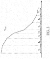
- FIG. 3 illustrates a waveform of an output signal V OUT of the integrating circuit 20 when an input signal V IN of the integrating circuit 20 is a DC (Direct Current) signal.
- the resistance value between the first terminal NR 1 and the second terminal NR 2 of the adjustable resistance module VR may be adjusted with respect to time intervals T 1 -T 7 by the control signals ctrl_R_1-ctrl_R_M, such that the integrating circuit 20 has different integration gains at the time intervals T 1 -T 7 .
- the time intervals T 1 , T 7 may have the smallest integration gain
- the time intervals T 2 , T 6 may have the second smallest integration gain
- the time interval T 4 at the center may have the largest integration gain.
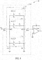
- FIG. 4 is a schematic diagram of an integrating circuit 40 according to an embodiment of the present invention.
- the integrating circuit 40 is similar to the integrating circuit 20, and thus, same components are denoted by the same symbols.
- the integrating circuit 40 is a switched-capacitor integrator.
- the integrating circuit 40 includes a switched-capacitor module SCM.
- the switched-capacitor module SCM is coupled between the negative input terminal of the operational amplifier Amp and the integrating input terminal N IN of the integrating circuit 40.
- the switched-capacitor module SCM includes an adjustable capacitance module VC and switches SW1-SW4.
- the switches SW1, SW2 are coupled to a first terminal NC 1 of the adjustable resistance module VC.
- the switches SW3, SW4 are coupled to a second terminal NC 2 of the adjustable resistance module VC.
- the switches SW2, SW4 are coupled to a ground.
- the adjustable capacitance module VC includes capacitor-selecting units CU 1 -CU N .
- the adjustable capacitance module VC is formed by the capacitor-selecting units CU 1 -CU N connected to each other in parallel, where any capacitor-selecting unit CU n within the capacitor-selecting units CU 1 -CU N includes a capacitor C n and a capacitance-control switch S Cn .
- the capacitance-control switch S Cn is controlled by a control signal ctrl_C_n.
- the capacitor-selecting unit CU n is formed by the capacitor C n connected to the capacitance-control switch S Cn in series.
- the control signals ctrl_C_1-ctrl_C_N may be configured to control the adjustable capacitance module VC, to adjust a capacitance value between the first terminal NC 1 and the second terminal of the adjustable capacitance module VC at the different time intervals, so as to change integration gain of the integrating circuit 40 at different time intervals.
- the switches SW1, SW2, SW3, SW4 may be controlled by frequency control signals ph1, ph2, where the frequency control signals ph1, ph2 are mutually orthogonal frequency control signals (i.e., time intervals of the frequency control signals ph1, ph2 being high voltage are not overlapped).
- the frequency control signal ph1 may be configured to control conduction status of the switches SW1, SW3, and the frequency control signal ph2 may be configured to control conduction status of the switches SW2, SW4.
- the frequency control signal ph1 may be configured to control conduction status of the switches SW1, SW4, and the frequency control signal ph2 may be configured to control conduction status of the switches SW2, SW3.
- the mutually orthogonal frequency control signals ph1, ph2 are utilized to control the conduction status of the switches SW1, SW2, SW3, SW4, requirements of present invention is satisfied, which is within the scope of present invention.
- the integrating circuit 20 and the integrating circuit 40 utilize the adjustable resistance module VR and the adjustable capacitance module VC to adjust the resistance value of the adjustable resistance module VR and the capacitance value of the adjustable capacitance module VC at the different time intervals.
- the integrating circuit 20 and the integrating circuit 40 may change the integration gains of the integrating circuit 20 and the integrating circuit 40 at the different time intervals, so as to realize an effect of window function. Therefore, the integrating circuit 20 and the integrating circuit 40 may reduce noise brought by sidelobe, so as to enhance an overall SNR (Signal to Noise Ratio).
- FIG. 5 is a schematic diagram of an integrating circuit 50 according to an embodiment of the present invention.
- the integrating circuit 50 is similar to the integrating circuit 20, and thus, same components are denoted by the same symbols. Different from the integrating circuit 20, the integrating circuit 50 includes an adjustable resistance module VR'.
- the adjustable resistance module VR' includes the resistor-selecting units RU 1 '-RU M '.
- the adjustable resistance module VR' is formed by the resistor-selecting units RU 1 '-RU M ' connected to each other in series, wherein any resistor-selecting unit RU m ' within the resistor-selecting units RU 1 '-RU M ' includes a resistor R m ' and a resistance-control switch S Rm '.
- FIG. 6 is a schematic diagram of an integrating circuit 60 according to an embodiment of the present invention.
- the integrating circuit 60 is similar to the integrating circuit 20, and thus, same components are denoted by the same symbols.
- the integrating circuit 60 includes a switched-capacitor module SCM'.
- the switched-capacitor module SCM' includes an adjustable capacitance module VC'.
- the adjustable capacitance module VC' includes the capacitor-selecting units CU 1 '-CU N '.
- the adjustable capacitance module VC' is formed by the capacitor-selecting units CU 1 '-CU N ' connected to each other in series, wherein any capacitor-selecting unit CU n ' within the capacitor-selecting units CU 1 '-CU N ' includes a capacitor C n ' and a capacitance-control switch S Cn '.
- the capacitance-control switch S Cn ' is controlled by a control signal ctrl_C_n'.
- the capacitor-selecting unit CU n ' is formed by the capacitor C n ' connected to the capacitance-control switch S Cn ' in parallel.
- FIG. 7 is a schematic diagram of an integrating circuit 70 according to an embodiment of the present invention.
- the integrating circuit 70 is similar to the integrating circuit 20, and thus, same components are denoted by the same symbols.
- the integrating circuit 70 includes an adjustable resistance module 700 and a switched-capacitor module 702.
- the adjustable resistance module 700 and the switched-capacitor module 702 are both coupled between the negative input terminal of the operational amplifier Amp and the integrating input terminal N IN of the integrating circuit 70, wherein the adjustable resistance module 700 may be realized by the adjustable resistance module VR or the adjustable resistance module VR', the switched-capacitor module 702 may be realized by the switched-capacitor module SCM or the switched-capacitor module SCM', which is not limited thereto.
- the switched-capacitor module is not limited to be realized by the switched-capacitor module SCM or the switched-capacitor module SCM' stated in the above.
- the switched-capacitor module may further include a resistor coupled between the switches SW1 and SW3.
- FIG. 8 is a schematic diagram of a switched-capacitor module 80 according to an embodiment of the present invention. Different from the switched-capacitor module SCM, SCM', the switched-capacitor module 80 further includes a resistor unit R coupled between the switches SW1 and SW3, where the resistor unit R may be one single resistor component or an adjustable resistance module , which is also within the scope of the present invention.
- FIG. 9 is a schematic diagram of an integrating circuit 90 according to an embodiment of the present invention.
- the integrating circuit 90 receives differential input signals V I+ , V I- and generates differential output signals V O+ , V O- .
- the integrating circuit 90 includes a full differential operational amplifier FOP, the integrating capacitors C I and C I ' and adjustable modules 900 and 900'.
- the adjustable module 900 and the adjustable module 900' may be realized by the adjustable resistance module VR, the adjustable resistance module VR', the switched-capacitor module SCM or the switched-capacitor module SCM'.
- the adjustable module 900 and the adjustable module 900' may also be realized by the adjustable resistance module VR (or the adjustable resistance module VR') connected to the switched-capacitor module SCM (or the switched-capacitor module SCM'), and not limited thereto.
- the resistance values or the capacitance values of the adjustable module 900 and the adjustable module 900' may be controlled to be the same/consistent, so as to balance the differential signals, which is to improve the performance of the integrating circuit 90.
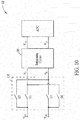
- FIG. 10 is a schematic diagram of a signal processing module 12 according to an embodiment of the present invention.
- the signal processing module 12 includes a switching mixer 120, the integrating circuit 90 and an analog-to-digital converter ADC.
- the switching mixer 120 receives differential signals V IN+ , V IN- and generates the differential input signals V I+ , V I- to the integrating circuit 90.
- the analog-to-digital converter ADC receives the differential output signals V O+ , V O- generated by the integrating circuit 90, and converts the analog differential output signals V O+ , V O- into digital signals for the back-end circuit to perform further computing operations.
- the switching mixer 120 may include switches S1-S4.
- the switches S1, S2 are configured to receive the differential signal V IN- .
- the switches S3, S4 are configured to receive the differential signal V IN+ .
- the switches S1, S4 are coupled to a first input terminal of the integrating circuit 90 to deliver the differential input signal V I- to the integrating circuit 90.
- the switches S2, S3 are coupled to a second input terminal of the integrating circuit 90 to deliver the differential input signal V I+ to the integrating circuit 90.
- FIG. 11 is a schematic diagram of an integrating circuit 14 according to an embodiment of the present invention.
- the integrating circuit 14 includes an adjustable integrating capacitor module 140, a voltage following module 142 and the operational amplifier Amp.
- the adjustable integrating capacitor module 140 is coupled between the positive and the negative input terminals and the output terminal of the operational amplifier Amp.
- the voltage following module 142 is coupled to the adjustable integrating capacitor module 140.
- the adjustable integrating capacitor module 140 includes integrating-capacitor-selecting units CIU 1 -CIU N .
- the adjustable integrating capacitor module 140 is regarded as being formed by the integrating-capacitor-selecting units CU 1 -CU N connected to each other in parallel.
- Any integrating-capacitor-selecting unit CIU n within the integrating-capacitor-selecting units CIU 1 -CIU N includes an integrating capacitor C In and the switches M n , J n .
- the integrating capacitor C In and the switches M n , J n are connected in series.
- the integrating capacitor C In is coupled to the positive and the negative input terminals of the operational amplifier Amp through the switch M n .
- the integrating capacitor C In is coupled to the output terminal of the operational amplifier Amp through the switch J n .
- the voltage following module 142 includes switches H 1 -H N , K 1 -K N and a voltage following circuit 144.
- the voltage following circuit 144 includes an operational amplifier OP.
- a negative input terminal (denoted as "-") of the operational amplifier OP is coupled to an output terminal of the operational amplifier OP.
- the output terminal of the operational amplifier OP is coupled to the switches K 1 -K N .
- a positive input terminal (denoted as "+”) is coupled to the switches H 1 -H N .
- the voltage following module 142 includes nodes ND 1 -ND N .
- the switches H 1 -H N are coupled to the switches K 1 -K N at the nodes ND 1 -ND N , respectively.
- a terminal of any switch H n within the switches H 1 -H N is coupled to the node ND n , and another terminal of the switch H n is coupled to the positive input terminal of the operational amplifier OP.
- a terminal of any switch K n within the switches K 1 -K N is coupled to the node ND n , and another terminal of the switch K n is coupled to the output terminal of the operational amplifier OP.
- Each node ND n within the nodes ND 1 -ND N is coupled between the integrating capacitor C In and the switch J n .
- the switches M 1 -M N , J 1 -J N , H 1 -H N , K 1 -K N may receive and be controlled by a plurality of control signals (not illustrated in FIG. 11 ) to perform integration operation, and the plurality of control signals may change the integration gain of the integrating circuit 14 at different time intervals, to adjust a capacitance value between the negative input terminal and the output terminal of the operational amplifier Amp, so as to realize the effect of the window function.
- the plurality of control signals controls the switches H 1 -H N , K 1 -K N to be cutoff.
- the plurality of control signals control the rest switches J 1 -J p-1 , J p+1 -J N to be cutoff.
- the plurality of control signals control a switch Mp corresponding to the integrating capacitor C Ip- among the switches M 1 -M N to conduct a connection between the integrating capacitor C Ip- and the negative input terminal of the operational amplifier Amp. Except the switch Mp, the plurality of control signals control the rest switches M 1 -M p-1 , M p+1 -M N to conduct connections between the integrating capacitor and the positive terminal of the operational amplifier Amp.
- the plurality of control signals control the switch Hp corresponding to the integrating capacitor C Ip and the switch K q corresponding to the integrating capacitor C Iq to be closed (i.e., the switches H p , Kq are conducted), and the rest switches H 1 -H p-1 , H p+1 -H N , K 1 -K q-1 , K q+1 -K N to be cutoff.
- the capacitance value between the negative input terminal and the output terminal of the operational amplifier Amp may be adjusted at the different time intervals, such that the integrating circuit 14 has different integration gains, so as to realize the effect of the window function.
- FIG. 12 is a schematic diagram of an integrating circuit 24 according to an embodiment of the present invention.
- the integrating circuit 24 is similar to the integrating circuit 14, and thus, same components are denoted by the same symbols.
- the integrating circuit 24 includes an adjustable integrating capacitor module 240.
- the adjustable integrating capacitor module 240 includes the integrating-capacitor-selecting units CIU 1 '-CIU N '.
- the adjustable integrating capacitor module 240 is formed by the integrating-capacitor-selecting units CIU 1 '-CIU N ' connected to each other in series.
- Any integrating-capacitor-selecting unit CIU n ' of the integrating-capacitor-selecting units CIU 1 '-CIU N ' includes an integrating capacitor C In ' and switches M n ', L n ', J n '.
- the integrating capacitor C In ' and the switches M n ', L n ' are connected in series.
- the integrating capacitor C In ' and the switches M n ', L n ' are connected as a series
- the switch J n ' is parallelly connected to the series formed by the integrating capacitor C In ' and the switches M n ', L n '.
- a switch M p ' corresponding to the integrating capacitor C Ip .' within the switches M 1 '-M N ' conducts a connection between the integrating capacitor C Ip- ' and the negative input terminal of the operational amplifier Amp.
- the switch Hp corresponding to the integrating capacitor C Ip ' and the switch K q corresponding to the integrating capacitor C Iq ' are closed (i.e., the switches H p , Kq are conducted), and the rest switches H 1 -H p-1 , H p+1 -H N , K 1 -K q-1 , K q+1 -K N are cutoff.
- a switch M q ' corresponding to the integrating capacitor C Iq ' within the switches M 1 '-M N ' conducts a connection between the integrating capacitor C Iq- ' and the positive input terminal of the operational amplifier Amp.
- the capacitance value between the negative input terminal and the output terminal of the operational amplifier Amp may be adjusted at the different time intervals, such that the integrating circuit 14 has different integration gains to realize the effect of the window function.
- the embodiments stated in the above are utilized for illustrating the best embodiments of the present invention, which is not limited thereto.
- the corresponding switch Mq is coupled to the positive input terminal of the operational amplifier Amp.
- Mq may be coupled to any reference voltage, and the reference voltage does not have to be the same as the positive input terminal of the operational amplifier Amp, which also brings different integration gain for the integrating circuit 14 to realize the effect of the window function.
- the switch may be coupled to any reference voltage, such that the integrating circuit 24 is utilized to realize the effect of the window function.
- the present invention utilizes the adjustable resistance module or the adjustable capacitance module to change the integration gain of the integrating circuit at the different time intervals, so as to realize the window function, reduce noise brought by sidelobe and enhance the SNR.
- the integrating circuit of the present invention may reduce a requirement of sampling rate of the analog-to-digital converter, such that the power consumption and complexity of the overall circuit are reduced.
Landscapes
- Engineering & Computer Science (AREA)
- Physics & Mathematics (AREA)
- Theoretical Computer Science (AREA)
- General Physics & Mathematics (AREA)
- General Engineering & Computer Science (AREA)
- Mathematical Physics (AREA)
- Power Engineering (AREA)
- Nonlinear Science (AREA)
- Computational Mathematics (AREA)
- Mathematical Analysis (AREA)
- Mathematical Optimization (AREA)
- Pure & Applied Mathematics (AREA)
- Human Computer Interaction (AREA)
- Software Systems (AREA)
- Data Mining & Analysis (AREA)
- Computer Hardware Design (AREA)
- Algebra (AREA)
- Operations Research (AREA)
- Databases & Information Systems (AREA)
- Amplifiers (AREA)
- Control Of Amplification And Gain Control (AREA)
- Networks Using Active Elements (AREA)
- Analogue/Digital Conversion (AREA)
Abstract
Description
- The present invention relates to an integrating circuit and a signal processing module, and more particularly, to an integrating circuit and a signal processing module capable of suppressing sidelobe.
- Match Filter and mixer are widely exploited in communication systems and capacitive touch control systems. In general, the mixer may be realized by a multiplier, which generates a multiplication result of a received signal and a local signal. In addition, the mixer may be further realized by a switching mixer with high linearity and low noise. The switching mixer is equivalent to multiplying the received signal by a square wave (i.e., the local signal). However, either the square wave or the sinusoidal wave has sidelobe in frequency domain, and an extra noise is brought in, such that a system SNR (Signal to Noise Ratio) is lowered. In order to solve problem of noise brought by the sidelobe, window function may be applied before the integrator. As
FIG. 1 shows, a signal SIG1 represents a waveform without applying any window function, and a signal SIG2 represents a waveform applying a window function e. As can be seen fromFIG. 1 , the window function e may be regarded as an envelop of the signal SIG2. Applying the window function e may effectively suppress noise brought by sidelobe, and enhance an anti-interference capability around the frequency band, such that the system SNR is enhanced. - The effect of window function may be realized by a digital integrator, where the digital integrator may use different integration gains at different time intervals, to achieve the effect of applying the window function. However, an output frequency of the digital integrator is higher, which is not suitable for the design of the back-end analog-to-digital converter (ADC). In other words, the back-end analog-to-digital converter needs to have sufficient high sampling rate to accurately perform sampling on the output signal of the digital integrator, where the power consumption and complexity of the circuit are raised. Therefore, it is necessary to improve the prior art.
- It is therefore a primary objective of the present invention to provide an integrating circuit and a signal processing module capable of suppressing sidelobe, to improve over disadvantages of the prior art.
- The present invention discloses an integrating circuit. The integrating circuit includes: an operational amplifier; an integrating capacitor, coupled to an output terminal and a first input terminal of the operational amplifier; and an adjustable resistance module, coupled between the first input terminal of the operational amplifier and an integrating input terminal of the integrating circuit. The adjustable resistance module receives a plurality of first control signals, to adjust a resistance value of the adjustable resistance module.
- The present invention further discloses an integrating circuit. The integrating circuit includes: an operational amplifier; an integrating capacitor, coupled to an output terminal and a first input terminal of the operational amplifier; and a switched-capacitor module, coupled between the first input terminal of the operational amplifier and the integrating input terminal of the integrating circuit. The switched-capacitor module includes an adjustable capacitance module, receiving a plurality of control signals, to adjust a capacitance value between a first terminal and a second terminal of the adjustable capacitance module; a first switch, coupled to the first terminal of the adjustable capacitance module; a second switch, coupled between the first terminal of the adjustable capacitance module and a ground; a third switch, coupled between the second terminal of the adjustable capacitance module and the first input terminal of the operational amplifier; and a fourth switch, coupled between the second terminal of the adjustable capacitance module and the ground.
- The present invention further discloses a signal processing module including a switching mixer; an analog-to-digital converter; an integrating circuit, coupled between the switching mixer and the analog-to-digital converter. The integrating circuit includes an operational amplifier; an integrating capacitor unit, coupled to an output terminal and a first input terminal of the operational amplifier; and an adjustable module, coupled between the first input terminal of the operational amplifier and an integrating input terminal of the integrating circuit. The adjustable module is controlled by a plurality of signals, to adjust a resistance value of a capacitance value of the adjustable module.
- The present invention further discloses an integrating circuit. The integrating circuit includes a first operational amplifier; an adjustable integrating capacitor module, coupled between a first input terminal and an output terminal of the first operational amplifier, wherein the adjustable integrating capacitor module includes a plurality of integrating-capacitor-selecting units, and each integrating-capacitor-selecting unit includes an integrating capacitor and at least a switch; and a voltage following module, coupled to the plurality of integrating-capacitor-selecting units of the adjustable integrating capacitor module; wherein the adjustable integrating capacitor module receives a plurality of control signals, to adjust a capacitance value between the first input terminal and the output terminal.
- By the integrating circuit provided by the present invention, the adjustable resistance module may be controlled by the control signals, to adjust a resistance value between the first terminal and the second terminal of the adjustable resistance module at different time intervals, so as to change the integration gain of the integrating circuit at the different time intervals; or the adjustable capacitance module may be controlled by the control signals, to adjust a capacitance value between the first terminal and the second terminal of the adjustable capacitance module at different time intervals, so as to change the integration gain of the integrating circuit at the different time intervals. The present invention utilizes analog integrator to realize the effect of window function, which may adjust the integration gain corresponding to different time intervals, reduce noise brought by sidelobe and enhance the SNR. Compared to the prior art, the integrating circuit of the present invention may reduce a requirement of sampling rate of the analog-to-digital converter, such that the power consumption and complexity of the overall circuit are reduced.
-
-
FIG. 1 is a schematic diagram of a plurality of waveforms. -
FIG. 2 is a schematic diagram of an integrating circuit according to an embodiment of the present invention. -
FIG. 3 is a waveform of an output signal of the integrating circuit ofFIG. 1 . -
FIG. 4 is a schematic diagram of an integrating circuit according to an embodiment of the present invention. -
FIG. 5 is a schematic diagram of an integrating circuit according to an embodiment of the present invention. -
FIG. 6 is a schematic diagram of an integrating circuit according to an embodiment of the present invention. -
FIG. 7 is a schematic diagram of an integrating circuit according to an embodiment of the present invention. -
FIG. 8 is a schematic diagram of a switched-capacitor module according to an embodiment of the present invention. -
FIG. 9 is a schematic diagram of an integrating circuit according to an embodiment of the present invention. -
FIG. 10 is a schematic diagram of a signal processing module according to an embodiment of the present invention. -
FIG. 11 is a schematic diagram of an integrating circuit according to an embodiment of the present invention. -
FIG. 12 is a schematic diagram of an integrating circuit according to an embodiment of the present invention. - The present invention utilizes an analog integrating circuit to realize an effect of window function, which is able to adjust different integration gains corresponding to different time intervals at the different time intervals. Please refer to
FIG. 2. FIG. 2 is a schematic diagram of anintegrating circuit 20 according to an embodiment of the present invention. The integratingcircuit 20 is a resistor-capacitor (RC) integrator, which includes an operational amplifier Amp, an integrating capacitor CI and an adjustable resistance module VR. The operational amplifier Amp includes a negative input terminal (denoted as "-"), a positive input terminal (denoted as "+") and an output terminal. The integrating capacitor CI is coupled between the negative input terminal and the output terminal of the operational amplifier Amp. The adjustable resistance module VR is coupled between the negative input terminal of the operational amplifier Amp and an integrating input terminal NIN of theintegrating circuit 20. The adjustable resistance module VR includes resistor-selecting units RU1-RUM. The adjustable resistance module VR is formed by the resistor-selecting units RU1-RUM connected to each other in parallel, wherein any resistor-selecting unit RUm of the resistor-selecting units RU1-RUM includes a resistor Rm and a resistance-control switch SRm. The resistance-control switch SRm is controlled by a control signal ctrl_R_m. The resistor-selecting unit RUm is formed by the resistor Rm connected to the resistance-control switch SRm in series. In other words, the control signals ctrl_R_1-ctrl_R_M may control the adjustable resistance module VR to adjust a resistance value between a first terminal NR1 and a second terminal NR2 of the adjustable resistance module VR, so as to change the integration gain of the integratingcircuit 20 at different time intervals. - Operation of the integrating
circuit 20 changing the integration gain at different time intervals may be referred toFIG. 3. FIG. 3 illustrates a waveform of an output signal VOUT of theintegrating circuit 20 when an input signal VIN of the integratingcircuit 20 is a DC (Direct Current) signal. As can be seen fromFIG. 3 , the resistance value between the first terminal NR1 and the second terminal NR2 of the adjustable resistance module VR may be adjusted with respect to time intervals T1-T7 by the control signals ctrl_R_1-ctrl_R_M, such that the integratingcircuit 20 has different integration gains at the time intervals T1-T7. To realize the window function, preferably, the time intervals T1, T7 may have the smallest integration gain, the time intervals T2, T6 may have the second smallest integration gain, and the time interval T4 at the center may have the largest integration gain. - In addition, please refer to
FIG. 4. FIG. 4 is a schematic diagram of anintegrating circuit 40 according to an embodiment of the present invention. The integratingcircuit 40 is similar to the integratingcircuit 20, and thus, same components are denoted by the same symbols. Different from the integratingcircuit 20, the integratingcircuit 40 is a switched-capacitor integrator. The integratingcircuit 40 includes a switched-capacitor module SCM. The switched-capacitor module SCM is coupled between the negative input terminal of the operational amplifier Amp and the integrating input terminal NIN of the integratingcircuit 40. The switched-capacitor module SCM includes an adjustable capacitance module VC and switches SW1-SW4. The switches SW1, SW2 are coupled to a first terminal NC1 of the adjustable resistance module VC. The switches SW3, SW4 are coupled to a second terminal NC2 of the adjustable resistance module VC. The switches SW2, SW4 are coupled to a ground. The adjustable capacitance module VC includes capacitor-selecting units CU1-CUN. The adjustable capacitance module VC is formed by the capacitor-selecting units CU1-CUN connected to each other in parallel, where any capacitor-selecting unit CUn within the capacitor-selecting units CU1-CUN includes a capacitor Cn and a capacitance-control switch SCn. The capacitance-control switch SCn is controlled by a control signal ctrl_C_n. The capacitor-selecting unit CUn is formed by the capacitor Cn connected to the capacitance-control switch SCn in series. In other words, the control signals ctrl_C_1-ctrl_C_N may be configured to control the adjustable capacitance module VC, to adjust a capacitance value between the first terminal NC1 and the second terminal of the adjustable capacitance module VC at the different time intervals, so as to change integration gain of the integratingcircuit 40 at different time intervals. - In addition, the switches SW1, SW2, SW3, SW4 may be controlled by frequency control signals ph1, ph2, where the frequency control signals ph1, ph2 are mutually orthogonal frequency control signals (i.e., time intervals of the frequency control signals ph1, ph2 being high voltage are not overlapped). Specifically, in an embodiment, the frequency control signal ph1 may be configured to control conduction status of the switches SW1, SW3, and the frequency control signal ph2 may be configured to control conduction status of the switches SW2, SW4. In another embodiment, the frequency control signal ph1 may be configured to control conduction status of the switches SW1, SW4, and the frequency control signal ph2 may be configured to control conduction status of the switches SW2, SW3. As long as the mutually orthogonal frequency control signals ph1, ph2 are utilized to control the conduction status of the switches SW1, SW2, SW3, SW4, requirements of present invention is satisfied, which is within the scope of present invention.
- As can be seen, the integrating
circuit 20 and the integratingcircuit 40 utilize the adjustable resistance module VR and the adjustable capacitance module VC to adjust the resistance value of the adjustable resistance module VR and the capacitance value of the adjustable capacitance module VC at the different time intervals. In other words, the integratingcircuit 20 and the integratingcircuit 40 may change the integration gains of the integratingcircuit 20 and the integratingcircuit 40 at the different time intervals, so as to realize an effect of window function. Therefore, the integratingcircuit 20 and the integratingcircuit 40 may reduce noise brought by sidelobe, so as to enhance an overall SNR (Signal to Noise Ratio). - It should be noted that, the embodiments stated in the above are utilized for illustrating the concept of the present invention. Those skilled in the art may make modifications and alternations accordingly, and not limited herein. For example, in the adjustable resistance module VR, the resistor-selecting units RU1-RUM are connected to each other in parallel, and the resistor Rm is connected to the resistance-control switch SRm in series. In the adjustable capacitance module VC, the capacitor-selecting units CU1-CUN are connected to each other in parallel, and the capacitor Cn is connected to the capacitance-control switch SCn, which is not limited thereto. Please refer to
FIG. 5. FIG. 5 is a schematic diagram of an integratingcircuit 50 according to an embodiment of the present invention. The integratingcircuit 50 is similar to the integratingcircuit 20, and thus, same components are denoted by the same symbols. Different from the integratingcircuit 20, the integratingcircuit 50 includes an adjustable resistance module VR'. The adjustable resistance module VR' includes the resistor-selecting units RU1'-RUM'. The adjustable resistance module VR' is formed by the resistor-selecting units RU1'-RUM' connected to each other in series, wherein any resistor-selecting unit RUm' within the resistor-selecting units RU1'-RUM' includes a resistor Rm' and a resistance-control switch SRm'. The resistance-control switch SRm' is controlled by a control signal ctrl_R_m'. The resistor-selecting unit RUm' is formed by the resistor Rm' connected to the resistance-control switch SRm' in parallel. Similarly, please refer toFIG. 6. FIG. 6 is a schematic diagram of an integratingcircuit 60 according to an embodiment of the present invention. The integratingcircuit 60 is similar to the integratingcircuit 20, and thus, same components are denoted by the same symbols. Different from the integratingcircuit 20, the integratingcircuit 60 includes a switched-capacitor module SCM'. The switched-capacitor module SCM' includes an adjustable capacitance module VC'. The adjustable capacitance module VC' includes the capacitor-selecting units CU1'-CUN'. The adjustable capacitance module VC' is formed by the capacitor-selecting units CU1'-CUN' connected to each other in series, wherein any capacitor-selecting unit CUn' within the capacitor-selecting units CU1'-CUN' includes a capacitor Cn' and a capacitance-control switch SCn'. The capacitance-control switch SCn' is controlled by a control signal ctrl_C_n'. The capacitor-selecting unit CUn' is formed by the capacitor Cn' connected to the capacitance-control switch SCn' in parallel. - In addition, the integrating circuit may include the adjustable resistance module and the adjustable capacitance module at the same time. For example, please refer to
FIG. 7. FIG. 7 is a schematic diagram of an integratingcircuit 70 according to an embodiment of the present invention. The integratingcircuit 70 is similar to the integratingcircuit 20, and thus, same components are denoted by the same symbols. The integratingcircuit 70 includes anadjustable resistance module 700 and a switched-capacitor module 702. Theadjustable resistance module 700 and the switched-capacitor module 702 are both coupled between the negative input terminal of the operational amplifier Amp and the integrating input terminal NIN of the integratingcircuit 70, wherein theadjustable resistance module 700 may be realized by the adjustable resistance module VR or the adjustable resistance module VR', the switched-capacitor module 702 may be realized by the switched-capacitor module SCM or the switched-capacitor module SCM', which is not limited thereto. - In addition, the switched-capacitor module is not limited to be realized by the switched-capacitor module SCM or the switched-capacitor module SCM' stated in the above. The switched-capacitor module may further include a resistor coupled between the switches SW1 and SW3. For example, please refer to
FIG. 8. FIG. 8 is a schematic diagram of a switched-capacitor module 80 according to an embodiment of the present invention. Different from the switched-capacitor module SCM, SCM', the switched-capacitor module 80 further includes a resistor unit R coupled between the switches SW1 and SW3, where the resistor unit R may be one single resistor component or an adjustable resistance module , which is also within the scope of the present invention. - In addition, the adjustable resistance module or the switched-capacitor module stated in the above are applied in the integrating circuit with a single-ended input, which is not limited thereto. The adjustable resistance module or the switched-capacitor module may be applied in an integrating circuit with differential input. For example, please refer to
FIG. 9. FIG. 9 is a schematic diagram of an integratingcircuit 90 according to an embodiment of the present invention. The integratingcircuit 90 receives differential input signals VI+, VI- and generates differential output signals VO+, VO-. The integratingcircuit 90 includes a full differential operational amplifier FOP, the integrating capacitors CI and CI' andadjustable modules 900 and 900'. Theadjustable module 900 and the adjustable module 900' may be realized by the adjustable resistance module VR, the adjustable resistance module VR', the switched-capacitor module SCM or the switched-capacitor module SCM'. In addition, theadjustable module 900 and the adjustable module 900' may also be realized by the adjustable resistance module VR (or the adjustable resistance module VR') connected to the switched-capacitor module SCM (or the switched-capacitor module SCM'), and not limited thereto. Preferably, the resistance values or the capacitance values of theadjustable module 900 and the adjustable module 900' may be controlled to be the same/consistent, so as to balance the differential signals, which is to improve the performance of the integratingcircuit 90. - In addition, the integrating
circuit 90 may be applied in a signal processing module. Please refer toFIG. 10. FIG. 10 is a schematic diagram of asignal processing module 12 according to an embodiment of the present invention. Thesignal processing module 12 includes a switchingmixer 120, the integratingcircuit 90 and an analog-to-digital converter ADC. The switchingmixer 120 receives differential signals VIN+, VIN- and generates the differential input signals VI+, VI- to the integratingcircuit 90. The analog-to-digital converter ADC receives the differential output signals VO+, VO- generated by the integratingcircuit 90, and converts the analog differential output signals VO+, VO- into digital signals for the back-end circuit to perform further computing operations. The switchingmixer 120 may include switches S1-S4. The switches S1, S2 are configured to receive the differential signal VIN-. The switches S3, S4 are configured to receive the differential signal VIN+. The switches S1, S4 are coupled to a first input terminal of the integratingcircuit 90 to deliver the differential input signal VI- to the integratingcircuit 90. The switches S2, S3 are coupled to a second input terminal of the integratingcircuit 90 to deliver the differential input signal VI+ to the integratingcircuit 90. - In addition, the integrating capacitor coupled between the input terminal and the output terminal of the operational amplifier Amp is realized by one single capacitor component, which is not limited thereto. The integrating capacitor coupled between the input terminal and the output terminal of the operational amplifier Amp may be realized by the adjustable capacitance module. Please refer to
FIG. 11. FIG. 11 is a schematic diagram of an integratingcircuit 14 according to an embodiment of the present invention. The integratingcircuit 14 includes an adjustable integratingcapacitor module 140, avoltage following module 142 and the operational amplifier Amp. The adjustable integratingcapacitor module 140 is coupled between the positive and the negative input terminals and the output terminal of the operational amplifier Amp. Thevoltage following module 142 is coupled to the adjustable integratingcapacitor module 140. Specifically, the adjustable integratingcapacitor module 140 includes integrating-capacitor-selecting units CIU1-CIUN. The adjustable integratingcapacitor module 140 is regarded as being formed by the integrating-capacitor-selecting units CU1-CUN connected to each other in parallel. Any integrating-capacitor-selecting unit CIUn within the integrating-capacitor-selecting units CIU1-CIUN includes an integrating capacitor CIn and the switches Mn, Jn. The integrating capacitor CIn and the switches Mn, Jn are connected in series. The integrating capacitor CIn is coupled to the positive and the negative input terminals of the operational amplifier Amp through the switch Mn. The integrating capacitor CIn is coupled to the output terminal of the operational amplifier Amp through the switch Jn. - In addition, the
voltage following module 142 includes switches H1-HN, K1-KN and a voltage following circuit 144. The voltage following circuit 144 includes an operational amplifier OP. A negative input terminal (denoted as "-") of the operational amplifier OP is coupled to an output terminal of the operational amplifier OP. The output terminal of the operational amplifier OP is coupled to the switches K1-KN. A positive input terminal (denoted as "+") is coupled to the switches H1-HN. In addition, thevoltage following module 142 includes nodes ND1-NDN. The switches H1-HN are coupled to the switches K1-KN at the nodes ND1-NDN, respectively. In other words, a terminal of any switch Hn within the switches H1-HN is coupled to the node NDn, and another terminal of the switch Hn is coupled to the positive input terminal of the operational amplifier OP. A terminal of any switch Kn within the switches K1-KN is coupled to the node NDn, and another terminal of the switch Kn is coupled to the output terminal of the operational amplifier OP. Each node NDn within the nodes ND1-NDN is coupled between the integrating capacitor CIn and the switch Jn. The switches M1-MN, J1-JN, H1-HN, K1-KN may receive and be controlled by a plurality of control signals (not illustrated inFIG. 11 ) to perform integration operation, and the plurality of control signals may change the integration gain of the integratingcircuit 14 at different time intervals, to adjust a capacitance value between the negative input terminal and the output terminal of the operational amplifier Amp, so as to realize the effect of the window function. - Detail operations of the integrating
circuit 14 are described as follows. When the integratingcircuit 14 performs integration on an integrating capacitor CIp of the integrating capacitors CI1-CIN, the plurality of control signals controls the switches H1-HN, K1-KN to be cutoff. In addition, among the switches J1-JN, except a switch Jp corresponding to the integrating capacitor CIp. is conducted, the plurality of control signals control the rest switches J1-Jp-1, Jp+1-JN to be cutoff. In addition, the plurality of control signals control a switch Mp corresponding to the integrating capacitor CIp- among the switches M1-MN to conduct a connection between the integrating capacitor CIp- and the negative input terminal of the operational amplifier Amp. Except the switch Mp, the plurality of control signals control the rest switches M1-Mp-1, Mp+1-MN to conduct connections between the integrating capacitor and the positive terminal of the operational amplifier Amp. Before the integratingcircuit 14 switches to perform integration on another integrating capacitor CIq of the integrating capacitors CI1-CIN from performing integration on the integrating capacitor CIp, the plurality of control signals control the switch Hp corresponding to the integrating capacitor CIp and the switch Kq corresponding to the integrating capacitor CIq to be closed (i.e., the switches Hp, Kq are conducted), and the rest switches H1-Hp-1, Hp+1-HN, K1-Kq-1, Kq+1-KN to be cutoff. Thus, the capacitance value between the negative input terminal and the output terminal of the operational amplifier Amp may be adjusted at the different time intervals, such that the integratingcircuit 14 has different integration gains, so as to realize the effect of the window function. - In addition, in the integrating
circuit 14, the adjustable integratingcapacitor module 140 is regarded as being formed by the integrating-capacitor-selecting units CIU1-CIUN connected to each other in parallel, which is not limited herein. Please refer toFIG. 12. FIG. 12 is a schematic diagram of an integratingcircuit 24 according to an embodiment of the present invention. The integratingcircuit 24 is similar to the integratingcircuit 14, and thus, same components are denoted by the same symbols. Different from the integratingcircuit 14, the integratingcircuit 24 includes an adjustable integratingcapacitor module 240. The adjustable integratingcapacitor module 240 includes the integrating-capacitor-selecting units CIU1'-CIUN'. The adjustable integratingcapacitor module 240 is formed by the integrating-capacitor-selecting units CIU1'-CIUN' connected to each other in series. Any integrating-capacitor-selecting unit CIUn' of the integrating-capacitor-selecting units CIU1'-CIUN' includes an integrating capacitor CIn' and switches Mn', Ln', Jn'. The integrating capacitor CIn' and the switches Mn', Ln' are connected in series. That is, the integrating capacitor CIn' and the switches Mn', Ln' are connected as a series, the switch Jn' is parallelly connected to the series formed by the integrating capacitor CIn' and the switches Mn', Ln'. - Detail operations of the integrating
circuit 24 are described as follows. When the integratingcircuit 24 performs integration on an integrating capacitor CIp' within the integrating capacitors CI1'-CIN', the switches H1-HN, K1-KN are cutoff. Within the switches J1'-JN', except the switch Jp' corresponding to the integrating capacitor CIp'- which is cutoff, the rest switches J1'-Jp-1', Jp+1'-JN' are conducted. In addition, the switch Lp' corresponding to the integrating capacitor CIp'. within the switches L1'-LN' are conducted. A switch Mp' corresponding to the integrating capacitor CIp.' within the switches M1'-MN' conducts a connection between the integrating capacitor CIp-' and the negative input terminal of the operational amplifier Amp. Before the integratingcircuit 24 switches to perform integration on another integrating capacitor CIq' within the integrating capacitors CI1'-CIN' from performing integration on the integrating capacitor CIp', the switch Hp corresponding to the integrating capacitor CIp' and the switch Kq corresponding to the integrating capacitor CIq' are closed (i.e., the switches Hp, Kq are conducted), and the rest switches H1-Hp-1, Hp+1-HN, K1-Kq-1, Kq+1-KN are cutoff. In addition, a switch Mq' corresponding to the integrating capacitor CIq' within the switches M1'-MN' conducts a connection between the integrating capacitor CIq-' and the positive input terminal of the operational amplifier Amp. Thus, the capacitance value between the negative input terminal and the output terminal of the operational amplifier Amp may be adjusted at the different time intervals, such that the integratingcircuit 14 has different integration gains to realize the effect of the window function. - Notably, the embodiments stated in the above are utilized for illustrating the best embodiments of the present invention, which is not limited thereto. For example, in
FIG. 11 , when the integrating capacitor CIq does not perform integration, the corresponding switch Mq is coupled to the positive input terminal of the operational amplifier Amp. In another embodiment (not illustrated), Mq may be coupled to any reference voltage, and the reference voltage does not have to be the same as the positive input terminal of the operational amplifier Amp, which also brings different integration gain for the integratingcircuit 14 to realize the effect of the window function. Similarly, when there is no integration performed on the integrating capacitor corresponding to the switches M1'-MN', the switch may be coupled to any reference voltage, such that the integratingcircuit 24 is utilized to realize the effect of the window function. - In summary, the present invention utilizes the adjustable resistance module or the adjustable capacitance module to change the integration gain of the integrating circuit at the different time intervals, so as to realize the window function, reduce noise brought by sidelobe and enhance the SNR. Compared to the prior art, the integrating circuit of the present invention may reduce a requirement of sampling rate of the analog-to-digital converter, such that the power consumption and complexity of the overall circuit are reduced.
- The foregoing is only preferred embodiments of the present invention, it is not intended to limit the present invention, any modifications within the spirit and principles of the present invention made, equivalent replacement and improvement, etc., should be included in this within the scope of the invention.
Claims (26)
- An integrating circuit, comprising:an operational amplifier;an integrating capacitor, coupled to an output terminal and a first input terminal of the operational amplifier; andan adjustable resistance module, coupled between the first input terminal of the operational amplifier and an integrating input terminal of the integrating circuit, wherein the adjustable resistance module is configured to receive a plurality of first control signals, to adjust a resistance value of the adjustable resistance module.
- The integrating circuit of claim 1, wherein the adjustable resistance module comprises a plurality of resistor-selecting units controlled by the plurality of first control signals respectively, and each resistor-selecting unit comprises:a resistor; anda resistance-control switch, coupled to the resistor.
- The integrating circuit of claim 2, wherein the plurality of resistor-selecting units are connected to each other in parallel, and the resistor and the resistance-control switch of each resistor-selecting unit are connected to each other in series.
- The integrating circuit of claim 2, wherein the plurality of resistor-selecting units are connected to each other in series, and the resistor and the resistance-control switch of each resistor-selecting unit are connected to each other in parallel.
- The integrating circuit of claim 1, further comprising a switched-capacitor module, coupled between the first input terminal of the operational amplifier and the integrating input terminal of the integrating circuit, the switched-capacitor module comprises:an adjustable capacitance module, configured to receive a plurality of second control signals, to adjust a capacitance value between a first terminal and a second terminal of the adjustable capacitance module;a first switch, coupled to the first terminal of the adjustable capacitance module;a second switch, coupled between the first terminal of the adjustable capacitance module and a ground;a third switch, coupled between the second terminal of the adjustable capacitance module and the first input terminal of the operational amplifier; anda fourth switch, coupled between the second terminal of the adjustable capacitance module and the ground.
- The integrating circuit of claim 5, wherein the adjustable capacitance module comprises a plurality of capacitor-selecting units controlled by the plurality of second control signals respectively, to adjust the capacitance value of the adjustable capacitance module, and each capacitor-selecting unit comprises:a capacitor; anda capacitance-control switch, coupled to the capacitor.
- The integrating circuit of claim 6, wherein the plurality of capacitor-selecting units are connected to each other in parallel, the capacitor and the capacitance-control switch of each capacitor-selecting unit are connected to each other in series; or wherein the plurality of capacitor-selecting units are connected to each other in series, the capacitor and the capacitance-control switch of each capacitor-selecting unit are connected to each other in parallel.
- The integrating circuit of claim 5, wherein the switched-capacitor module further comprises:at least a resistor unit, coupled between the first switch and the third switch.
- An integrating circuit, comprising:an operational amplifier;an integrating capacitor, coupled to an output terminal and a first input terminal of the operational amplifier; anda switched-capacitor module, coupled between the first input terminal of the operational amplifier and an integrating input terminal of the integrating circuit, the switched-capacitor module comprises:an adjustable capacitance module, configured to receive a plurality of control signals, to adjust a capacitance value between a first terminal and a second terminal of the adjustable capacitance module;a first switch, coupled to the first terminal of the adjustable capacitance module;a second switch, coupled between the first terminal of the adjustable capacitance module and a ground;a third switch, coupled between the second terminal of the adjustable capacitance module and the first input terminal of the operational amplifier; anda fourth switch, coupled between the second terminal of the adjustable capacitance module and the ground.
- The integrating circuit of claim 9, wherein the adjustable capacitance module comprises a plurality of capacitor-selecting units controlled by the plurality of control signals respectively, and each capacitor-selecting unit comprises:a capacitor; anda capacitance-control switch, coupled to the capacitor.
- The integrating circuit of claim 10, wherein the plurality of capacitor-selecting units are connected to each other in parallel, the capacitor and the capacitance-control switch of each capacitor-selecting unit are connected to each other in series; or wherein the plurality of capacitor-selecting units are connected to each other in series, the capacitor and the capacitance-control switch of each capacitor-selecting unit are connected to each other in parallel.
- The integrating circuit of claim 9, wherein the switched-capacitor module further comprises:at least a resistor unit, coupled between the first switch and the third switch.
- A signal processing module, comprising:a switching mixer;an analog-to-digital converter;an integrating circuit, coupled between the switching mixer and the analog-to-digital converter, the integrating circuit comprises:an operational amplifier;an integrating capacitor unit, coupled to an output terminal and a first input terminal of the operational amplifier; andan adjustable module, coupled between the first input terminal of the operational amplifier and an integrating input terminal of the integrating circuit, wherein the adjustable module is controlled by a plurality of signals, to adjust a resistance value or a capacitance value of the adjustable module.
- The signal processing module of claim 13, wherein the adjustable module comprises an adjustable resistance module, and the adjustable resistance module is configured to receive a plurality of first control signals, to adjust the resistance value of the adjustable resistance module.
- The signal processing module of claim 14, wherein the adjustable resistance module comprises a plurality of resistor-selecting units controlled by the plurality of first control signals respectively, and each resistor-selecting unit comprises:a resistor; anda resistance-control switch, coupled to the resistor.
- The signal processing module of claim 15, wherein the plurality of resistor-selecting units are connected to each other in parallel, and the resistor and the resistance-control switch of each resistor-selecting unit are connected to each other in series signal; or wherein the plurality of resistor-selecting units are connected to each other in series, and the resistor and the resistance-control switch of each resistor-selecting unit are connected to each other in parallel.
- The signal processing module of claim 13, wherein the adjustable module comprises a switched-capacitor module, coupled between the first input terminal of the operational amplifier and the integrating input terminal of the integrating circuit, and the switched-capacitor module comprises:an adjustable capacitance module, configured to receive a plurality of second control signals, to adjust a capacitance value between a first terminal and a second terminal of the adjustable capacitance module;a first switch, coupled to the first terminal;a second switch, coupled between the first terminal and a ground;a third switch, coupled between the second terminal and the first input terminal of the operational amplifier; anda fourth switch, coupled between the second terminal and the ground.
- The signal processing module of claim 17, wherein the adjustable capacitance module comprises a plurality of capacitor-selecting units controlled by the plurality of second control signals respectively, and each capacitor-selecting unit comprises:a capacitor; anda capacitance-control switch, coupled to the capacitor.
- The signal processing module of claim 18, wherein the plurality of capacitor-selecting units are connected to each other in parallel, the capacitor and the capacitance-control switch of each capacitor-selecting unit are connected to each other in series signal; or wherein the plurality of capacitor-selecting units are connected to each other in series, the capacitor and the capacitance-control switch of each capacitor-selecting unit are connected to each other in parallel.
- The signal processing module of claim 17, wherein the switched-capacitor module further comprises:at least a resistor unit, coupled between the first switch and the third switch.
- An integrating circuit, comprising:a first operational amplifier;an adjustable integrating capacitor module, coupled between a first input terminal and an output terminal of the first operational amplifier, wherein the adjustable integrating capacitor module comprises a plurality of integrating-capacitor-selecting units, and each integrating-capacitor-selecting unit comprises an integrating capacitor and at least a switch; anda voltage following module, coupled to the plurality of integrating-capacitor-selecting units of the adjustable integrating capacitor module;wherein the adjustable integrating capacitor module is configured to receive a plurality of control signals, to adjust a capacitance value between the first input terminal and the output terminal.
- The integrating circuit of claim 21, wherein the voltage following module comprises a plurality of nodes, and the plurality of nodes are electrically connected to the integrating capacitors of the plurality of integrating-capacitor-selecting units, respectively.
- The integrating circuit of claim 22, wherein the voltage following module comprises a voltage following circuit, and each node of the plurality of nodes is coupled to an input terminal of the voltage following circuit through a first switch and coupled to an output terminal of the voltage following circuit through a second switch.
- The integrating circuit of claim 23, wherein the voltage following circuit comprises a second operational amplifier, wherein a first input terminal of the second operational amplifier is electrically connected to an output terminal of the second operational amplifier, a second input terminal of the operational amplifier is the input terminal of the voltage following circuit, and an output terminal of the operational amplifier is the output terminal of the voltage following circuit.
- The integrating circuit of claim 21, wherein the plurality of integrating-capacitor-selecting units are connected to each other in parallel.
- The integrating circuit of claim 21, wherein the plurality of integrating-capacitor-selecting units are coupled to each other in series.
Applications Claiming Priority (1)
| Application Number | Priority Date | Filing Date | Title |
|---|---|---|---|
| PCT/CN2016/078308 WO2017166286A1 (en) | 2016-04-01 | 2016-04-01 | Integrator circuit and signal processing module |
Publications (2)
| Publication Number | Publication Date |
|---|---|
| EP3252581A1 true EP3252581A1 (en) | 2017-12-06 |
| EP3252581A4 EP3252581A4 (en) | 2018-04-18 |
Family
ID=59962518
Family Applications (2)
| Application Number | Title | Priority Date | Filing Date |
|---|---|---|---|
| EP16889664.5A Withdrawn EP3252581A4 (en) | 2016-04-01 | 2016-04-01 | Integrator circuit and signal processing module |
| EP17758788.8A Active EP3267298B1 (en) | 2016-04-01 | 2017-03-31 | Window function processing module |
Family Applications After (1)
| Application Number | Title | Priority Date | Filing Date |
|---|---|---|---|
| EP17758788.8A Active EP3267298B1 (en) | 2016-04-01 | 2017-03-31 | Window function processing module |
Country Status (5)
| Country | Link |
|---|---|
| US (2) | US20180026608A1 (en) |
| EP (2) | EP3252581A4 (en) |
| KR (2) | KR20170131380A (en) |
| CN (2) | CN107850970B (en) |
| WO (2) | WO2017166286A1 (en) |
Families Citing this family (9)
| Publication number | Priority date | Publication date | Assignee | Title |
|---|---|---|---|---|
| CN107850970B (en) | 2016-04-01 | 2021-04-27 | 深圳市汇顶科技股份有限公司 | Integrating circuit and signal processing module |
| US10644675B2 (en) * | 2017-10-02 | 2020-05-05 | Robert Bosch Gmbh | Switched resistance device with reduced sensitivity to parasitic capacitance |
| US11120230B2 (en) | 2018-09-20 | 2021-09-14 | Sendyne Corporation | Analog computing using dynamic amplitude scaling and methods of use |
| CN111193503A (en) * | 2018-10-26 | 2020-05-22 | 长鑫存储技术有限公司 | Transistor switching circuit, regulating method and storage device |
| CN111565032B (en) * | 2019-02-13 | 2023-11-10 | 上海耕岩智能科技有限公司 | Signal conversion circuit and signal readout circuit architecture |
| US10733391B1 (en) * | 2019-03-08 | 2020-08-04 | Analog Devices International Unlimited Company | Switching scheme for low offset switched-capacitor integrators |
| US11226706B2 (en) | 2020-01-13 | 2022-01-18 | Cypress Semiconductor Corporation | Low-emissions touch controller |
| US11307712B2 (en) * | 2020-04-07 | 2022-04-19 | Cypress Semiconductor Corporation | Systems, methods, and devices for capacitive sensing with sinusoidal demodulation |
| CN113541692A (en) * | 2021-08-17 | 2021-10-22 | 北京华峰测控技术股份有限公司 | Integrating circuit and source measurement module |
Family Cites Families (28)
| Publication number | Priority date | Publication date | Assignee | Title |
|---|---|---|---|---|
| US5245646A (en) * | 1992-06-01 | 1993-09-14 | Motorola, Inc. | Tuning circuit for use with an integrated continuous time analog filter |
| DE69419897T2 (en) * | 1994-04-21 | 2000-05-31 | Stmicroelectronics S.R.L., Agrate Brianza | Low-distortion circuit with switched capacitances |
| FR2879373A1 (en) * | 2004-12-14 | 2006-06-16 | St Microelectronics Sa | Integrated circuit, has calibrating circuit producing adjustment value for resistor of pair of components to compensate error on resistor and capacitor product, where value is then applied to capacitor of another pair of components |
| JP2011041172A (en) * | 2009-08-18 | 2011-02-24 | Ricoh Co Ltd | Electronic volume circuit |
| TWI397843B (en) * | 2009-10-30 | 2013-06-01 | Orise Technology Co Ltd | Touch panel sensing circuit |
| JP5834377B2 (en) * | 2010-01-13 | 2015-12-24 | 富士通株式会社 | Filter circuit |
| JP2011188250A (en) * | 2010-03-09 | 2011-09-22 | Renesas Electronics Corp | Time constant adjustment circuit |
| CN101873182A (en) * | 2010-06-17 | 2010-10-27 | 复旦大学 | A Fast Multi-Resolution Spectrum Sensing Module |
| CN102299716A (en) * | 2010-06-22 | 2011-12-28 | 君曜科技股份有限公司 | Sample-and-hold circuit and touch sensing device thereof |
| JP5622596B2 (en) * | 2011-01-13 | 2014-11-12 | アルプス電気株式会社 | Capacity detector |
| US9086439B2 (en) * | 2011-02-25 | 2015-07-21 | Maxim Integrated Products, Inc. | Circuits, devices and methods having pipelined capacitance sensing |
| CN102707821B (en) * | 2011-03-28 | 2015-04-22 | 深圳市汇顶科技股份有限公司 | Method and system for de-noising touch detection device |
| KR101919056B1 (en) * | 2011-04-28 | 2018-11-15 | 가부시키가이샤 한도오따이 에네루기 켄큐쇼 | Semiconductor circuit |
| US8766939B2 (en) * | 2012-01-09 | 2014-07-01 | Broadcom Corporation | Highly configurable analog preamp with analog to digital converter |
| US9141239B2 (en) * | 2012-02-07 | 2015-09-22 | Zinitix | Touch screen device, and driving device and driving method for touch panel using predetermined binary sequences |
| JP2013236204A (en) * | 2012-05-08 | 2013-11-21 | Seiko Epson Corp | Circuit device and electronic apparatus |
| KR101444524B1 (en) * | 2012-07-09 | 2014-09-24 | 삼성전기주식회사 | Apparatus and method for sensing capacitance, and touchscreen apparatus |
| US8982093B2 (en) * | 2012-12-20 | 2015-03-17 | Broadcom Corporation | Capacitive touch sensing system with interference rejection |
| CN203014760U (en) * | 2012-12-31 | 2013-06-19 | 上海贝岭股份有限公司 | Active filter |
| CN105144576B (en) * | 2013-03-04 | 2019-06-11 | 爱德万测试公司 | Switchable signal routing circuit, method and non-transitory storage medium |
| US8890841B2 (en) | 2013-03-13 | 2014-11-18 | 3M Innovative Properties Company | Capacitive-based touch apparatus and method therefor, with reduced interference |
| US9001066B2 (en) * | 2013-05-06 | 2015-04-07 | Rajkumari Mohindra | PAPR optimized OFDM touch engine with tone spaced windowed demodulation |
| TWI488099B (en) * | 2013-06-20 | 2015-06-11 | 財團法人工業技術研究院 | Touch device and sensing compensation method |
| US20150180493A1 (en) * | 2013-12-23 | 2015-06-25 | Yu-Ren Liu | Capacitor Sensor Circuit with Rectifier and Integrator |
| WO2016032704A1 (en) * | 2014-08-25 | 2016-03-03 | 3M Innovative Properties Company | Capacitive-based touch apparatus and method with reduced interference |
| CN204386337U (en) * | 2015-01-09 | 2015-06-10 | 成都数云科技有限公司 | A kind of temperature control automatic window control circuit |
| WO2016170622A1 (en) * | 2015-04-22 | 2016-10-27 | オリンパス株式会社 | Semiconductor device |
| CN107850970B (en) | 2016-04-01 | 2021-04-27 | 深圳市汇顶科技股份有限公司 | Integrating circuit and signal processing module |
-
2016
- 2016-04-01 CN CN201680000590.5A patent/CN107850970B/en active Active
- 2016-04-01 WO PCT/CN2016/078308 patent/WO2017166286A1/en not_active Ceased
- 2016-04-01 KR KR1020177024169A patent/KR20170131380A/en not_active Ceased
- 2016-04-01 EP EP16889664.5A patent/EP3252581A4/en not_active Withdrawn
-
2017
- 2017-03-31 CN CN201780000819.XA patent/CN107438951B/en active Active
- 2017-03-31 KR KR1020177025951A patent/KR101965274B1/en active Active
- 2017-03-31 WO PCT/CN2017/079113 patent/WO2017167297A1/en not_active Ceased
- 2017-03-31 EP EP17758788.8A patent/EP3267298B1/en active Active
- 2017-08-17 US US15/679,182 patent/US20180026608A1/en not_active Abandoned
- 2017-09-06 US US15/696,195 patent/US10367478B2/en active Active
Also Published As
| Publication number | Publication date |
|---|---|
| KR20170126467A (en) | 2017-11-17 |
| EP3267298A1 (en) | 2018-01-10 |
| WO2017166286A1 (en) | 2017-10-05 |
| CN107438951A (en) | 2017-12-05 |
| US20180013410A1 (en) | 2018-01-11 |
| EP3267298A4 (en) | 2018-04-18 |
| EP3267298B1 (en) | 2020-11-18 |
| KR101965274B1 (en) | 2019-04-03 |
| WO2017167297A1 (en) | 2017-10-05 |
| EP3252581A4 (en) | 2018-04-18 |
| CN107850970B (en) | 2021-04-27 |
| US10367478B2 (en) | 2019-07-30 |
| KR20170131380A (en) | 2017-11-29 |
| CN107850970A (en) | 2018-03-27 |
| CN107438951B (en) | 2020-12-15 |
| US20180026608A1 (en) | 2018-01-25 |
Similar Documents
| Publication | Publication Date | Title |
|---|---|---|
| US20180026608A1 (en) | Integrating Circuit and Signal Processing Module | |
| CN107104648B (en) | amplifying circuit | |
| CN103297057A (en) | Sigma-Delta Modulator and Method for Converting Analog Signals to Digital Signals | |
| TW201308889A (en) | Infinite impulse response (IIR) filter and filtering method | |
| US12206430B2 (en) | A/D converter | |
| EP0415080A2 (en) | Device for converting unbalanced analog electric signals into fully-differential signals | |
| US8199040B2 (en) | Analog-to-digital converter | |
| US10331409B2 (en) | Sine wave multiplication device and input device having the same | |
| US20170085251A1 (en) | Preamplifier | |
| US6441762B2 (en) | Circuit device for cancelling out spurious pulses in a switched capacitance low-pass filter, and a filter incorporating it | |
| JP2011019156A (en) | Chopper amplifier | |
| US8030991B2 (en) | Frequency tuning and direct current offset canceling circuit for continuous-time analog filter with time divided | |
| KR20190021634A (en) | Discrete-time integrator circuit with operational amplifier gain compensation function | |
| CN110557098A (en) | positive feedback transimpedance amplification circuit and adjustment method | |
| US20040232970A1 (en) | Level shift circuit | |
| CN110277994B (en) | Anti-aliasing filter for discretization over the sampling period | |
| Singh et al. | Switched-capacitor filter design for ECG application using 180nm CMOS technology | |
| CN111969963B (en) | Pre-amplifier | |
| CN112633020A (en) | Device for calculating product sum | |
| US5760728A (en) | Input stage for an analog-to-digital converter and method of operation thereof | |
| CN110504940B (en) | Low-pass filter circuit and method | |
| CN1783857B (en) | Device for clearing DC bias voltage and regulating gain | |
| US10044368B2 (en) | Sigma delta analog to digital converter | |
| EP3285445B1 (en) | Multiple sampling stage line receiver and related methods | |
| CN120200564A (en) | Amplifier Circuit |
Legal Events
| Date | Code | Title | Description |
|---|---|---|---|
| PUAI | Public reference made under article 153(3) epc to a published international application that has entered the european phase |
Free format text: ORIGINAL CODE: 0009012 |
|
| 17P | Request for examination filed |
Effective date: 20170817 |
|
| AK | Designated contracting states |
Kind code of ref document: A1 Designated state(s): AL AT BE BG CH CY CZ DE DK EE ES FI FR GB GR HR HU IE IS IT LI LT LU LV MC MK MT NL NO PL PT RO RS SE SI SK SM TR |
|
| AX | Request for extension of the european patent |
Extension state: BA ME |
|
| R17P | Request for examination filed (corrected) |
Effective date: 20170817 |
|
| A4 | Supplementary search report drawn up and despatched |
Effective date: 20180320 |
|
| RIC1 | Information provided on ipc code assigned before grant |
Ipc: G06F 3/044 20060101AFI20180314BHEP Ipc: G06F 3/041 20060101ALI20180314BHEP Ipc: H03F 3/00 20060101ALI20180314BHEP |
|
| STAA | Information on the status of an ep patent application or granted ep patent |
Free format text: STATUS: THE APPLICATION HAS BEEN WITHDRAWN |
|
| 18W | Application withdrawn |
Effective date: 20180914 |