EP3252570A1 - Electronic pen - Google Patents
Electronic pen Download PDFInfo
- Publication number
- EP3252570A1 EP3252570A1 EP16743081.8A EP16743081A EP3252570A1 EP 3252570 A1 EP3252570 A1 EP 3252570A1 EP 16743081 A EP16743081 A EP 16743081A EP 3252570 A1 EP3252570 A1 EP 3252570A1
- Authority
- EP
- European Patent Office
- Prior art keywords
- electronic pen
- core body
- signal
- tip
- circuit
- Prior art date
- Legal status (The legal status is an assumption and is not a legal conclusion. Google has not performed a legal analysis and makes no representation as to the accuracy of the status listed.)
- Granted
Links
Images






Classifications
-
- G—PHYSICS
- G06—COMPUTING OR CALCULATING; COUNTING
- G06F—ELECTRIC DIGITAL DATA PROCESSING
- G06F3/00—Input arrangements for transferring data to be processed into a form capable of being handled by the computer; Output arrangements for transferring data from processing unit to output unit, e.g. interface arrangements
- G06F3/01—Input arrangements or combined input and output arrangements for interaction between user and computer
- G06F3/03—Arrangements for converting the position or the displacement of a member into a coded form
- G06F3/033—Pointing devices displaced or positioned by the user, e.g. mice, trackballs, pens or joysticks; Accessories therefor
- G06F3/0354—Pointing devices displaced or positioned by the user, e.g. mice, trackballs, pens or joysticks; Accessories therefor with detection of two-dimensional [2D] relative movements between the device, or an operating part thereof, and a plane or surface, e.g. 2D mice, trackballs, pens or pucks
- G06F3/03545—Pens or stylus
-
- G—PHYSICS
- G06—COMPUTING OR CALCULATING; COUNTING
- G06F—ELECTRIC DIGITAL DATA PROCESSING
- G06F3/00—Input arrangements for transferring data to be processed into a form capable of being handled by the computer; Output arrangements for transferring data from processing unit to output unit, e.g. interface arrangements
- G06F3/01—Input arrangements or combined input and output arrangements for interaction between user and computer
- G06F3/03—Arrangements for converting the position or the displacement of a member into a coded form
- G06F3/033—Pointing devices displaced or positioned by the user, e.g. mice, trackballs, pens or joysticks; Accessories therefor
- G06F3/038—Control and interface arrangements therefor, e.g. drivers or device-embedded control circuitry
- G06F3/0383—Signal control means within the pointing device
-
- G—PHYSICS
- G06—COMPUTING OR CALCULATING; COUNTING
- G06F—ELECTRIC DIGITAL DATA PROCESSING
- G06F3/00—Input arrangements for transferring data to be processed into a form capable of being handled by the computer; Output arrangements for transferring data from processing unit to output unit, e.g. interface arrangements
- G06F3/01—Input arrangements or combined input and output arrangements for interaction between user and computer
- G06F3/03—Arrangements for converting the position or the displacement of a member into a coded form
- G06F3/041—Digitisers, e.g. for touch screens or touch pads, characterised by the transducing means
- G06F3/0416—Control or interface arrangements specially adapted for digitisers
- G06F3/04162—Control or interface arrangements specially adapted for digitisers for exchanging data with external devices, e.g. smart pens, via the digitiser sensing hardware
-
- G—PHYSICS
- G06—COMPUTING OR CALCULATING; COUNTING
- G06F—ELECTRIC DIGITAL DATA PROCESSING
- G06F3/00—Input arrangements for transferring data to be processed into a form capable of being handled by the computer; Output arrangements for transferring data from processing unit to output unit, e.g. interface arrangements
- G06F3/01—Input arrangements or combined input and output arrangements for interaction between user and computer
- G06F3/03—Arrangements for converting the position or the displacement of a member into a coded form
- G06F3/041—Digitisers, e.g. for touch screens or touch pads, characterised by the transducing means
- G06F3/044—Digitisers, e.g. for touch screens or touch pads, characterised by the transducing means by capacitive means
-
- G—PHYSICS
- G06—COMPUTING OR CALCULATING; COUNTING
- G06F—ELECTRIC DIGITAL DATA PROCESSING
- G06F3/00—Input arrangements for transferring data to be processed into a form capable of being handled by the computer; Output arrangements for transferring data from processing unit to output unit, e.g. interface arrangements
- G06F3/01—Input arrangements or combined input and output arrangements for interaction between user and computer
- G06F3/03—Arrangements for converting the position or the displacement of a member into a coded form
- G06F3/041—Digitisers, e.g. for touch screens or touch pads, characterised by the transducing means
- G06F3/044—Digitisers, e.g. for touch screens or touch pads, characterised by the transducing means by capacitive means
- G06F3/0441—Digitisers, e.g. for touch screens or touch pads, characterised by the transducing means by capacitive means using active external devices, e.g. active pens, for receiving changes in electrical potential transmitted by the digitiser, e.g. tablet driving signals
-
- G—PHYSICS
- G06—COMPUTING OR CALCULATING; COUNTING
- G06F—ELECTRIC DIGITAL DATA PROCESSING
- G06F3/00—Input arrangements for transferring data to be processed into a form capable of being handled by the computer; Output arrangements for transferring data from processing unit to output unit, e.g. interface arrangements
- G06F3/01—Input arrangements or combined input and output arrangements for interaction between user and computer
- G06F3/03—Arrangements for converting the position or the displacement of a member into a coded form
- G06F3/041—Digitisers, e.g. for touch screens or touch pads, characterised by the transducing means
- G06F3/044—Digitisers, e.g. for touch screens or touch pads, characterised by the transducing means by capacitive means
- G06F3/0442—Digitisers, e.g. for touch screens or touch pads, characterised by the transducing means by capacitive means using active external devices, e.g. active pens, for transmitting changes in electrical potential to be received by the digitiser
-
- G—PHYSICS
- G06—COMPUTING OR CALCULATING; COUNTING
- G06F—ELECTRIC DIGITAL DATA PROCESSING
- G06F3/00—Input arrangements for transferring data to be processed into a form capable of being handled by the computer; Output arrangements for transferring data from processing unit to output unit, e.g. interface arrangements
- G06F3/01—Input arrangements or combined input and output arrangements for interaction between user and computer
- G06F3/03—Arrangements for converting the position or the displacement of a member into a coded form
- G06F3/041—Digitisers, e.g. for touch screens or touch pads, characterised by the transducing means
- G06F3/046—Digitisers, e.g. for touch screens or touch pads, characterised by the transducing means by electromagnetic means
-
- G—PHYSICS
- G06—COMPUTING OR CALCULATING; COUNTING
- G06F—ELECTRIC DIGITAL DATA PROCESSING
- G06F2203/00—Indexing scheme relating to G06F3/00 - G06F3/048
- G06F2203/038—Indexing scheme relating to G06F3/038
- G06F2203/0384—Wireless input, i.e. hardware and software details of wireless interface arrangements for pointing devices
-
- G—PHYSICS
- G06—COMPUTING OR CALCULATING; COUNTING
- G06F—ELECTRIC DIGITAL DATA PROCESSING
- G06F2203/00—Indexing scheme relating to G06F3/00 - G06F3/048
- G06F2203/041—Indexing scheme relating to G06F3/041 - G06F3/045
- G06F2203/04105—Pressure sensors for measuring the pressure or force exerted on the touch surface without providing the touch position
Definitions
- the present invention relates to an electronic pen that is a pen-type position indicator used with a position detecting device.
- the electronic pen is held by a user and is used for position indication over a sensor of a position detecting device.
- the indicated position over the sensor by this electronic pen is detected by the position detecting device through transfer of a signal for position detection between the electronic pen and a sensor based on various coupling systems such as the electromagnetic induction coupling system and the capacitive coupling system.
- Patent Document 1 Japanese Patent Laid-Open No. 2014-67265
- Patent Document 1 Japanese Patent Laid-Open No. 2014-67265
- Identification information and so forth as additional information of an electronic pen is information of such a nature that the information should be kept secret if possible, and is information for which security management is required if possible. Furthermore, these pieces of additional information are information that should be sent out to a position detecting device when a user is carrying out position indication operation over a sensor by the electronic pen, and should not be unnecessarily transmitted if possible. However, in the past, it has been general that the additional information is also simultaneously sent out with a signal for position detection and there has been a problem that no consideration is made about ensuring of security of the additional information and transmission only at the time of need.
- the recent electronic pens have been decreasing in thickness in consideration of being so used as to be mounted on small-size portable equipment such as a mobile phone terminal in which a position detecting device is incorporated.
- thickness reduction is being promoted also in the core body that is incorporated in the electronic pen and forms the pen tip.
- the core body is attached in the state in which its tip protrudes from one opening of a tubular chassis of the electronic pen.
- the core body becomes vulnerable to a shock due to this thickness reduction, and there is the case in which the core body gets broken or distorted when the electronic pen is dropped.
- the material of the core body is felt.
- this felt is obtained by bundling and bonding fibers and therefore the strength is slightly low.
- the bundle breaks up when an excessive force such as a shock due to a drop is applied to the core body.
- the core body of felt is vulnerable to a large force in a direction perpendicular to the core axis. Therefore, it is important to protect the core body when the electronic pen is not used.
- the present invention intends to provide an electronic pen configured to be capable of simultaneously solving problems of ensuring of security of additional information and avoidance of unnecessary transmission and protection of protection of a core body.
- an invention of claim 1 provides an electronic pen that transmits a signal to a sensor of a position detecting device and is characterized by including a core body, a signal transmitting unit that transmits a signal to the sensor, a protection mechanism that sets at least a tip of the core body to a state of being not exposed to the external to protect at least the tip of the core body, and detecting means that detects whether or not at least the tip of the core body is in a state of being protected by the protection mechanism.
- a signal for position detection and a signal including additional information that is to be transmitted to the position detecting device when position indication operation is carried out over the sensor are allowed to be transmitted from the signal transmitting unit when at least the tip of the core body is not protected by the protection mechanism and is exposed to the external, and the signal including the additional information is precluded from being transmitted when at least the tip of the core body is protected by the protection mechanism.
- the core body can be protected by the protection mechanism as the state in which the core body does not protrude to the external when this electronic pen is not used.
- the core body can be protected from shock of a drop or the like.
- the additional information is precluded from being sent out based on the detection result.
- the additional information is allowed to be transmitted.
- the transmission of the additional information is precluded when the tip of the core body is protected by the protection mechanism, and the transmission of the additional information is allowed when the protection of the tip of the core body by the protection mechanism is released.
- This can provide an electronic pen configured to be capable of simultaneously solving problems of ensuring of security of the additional information and avoidance of unnecessary transmission and protection of protection of the core body.
- FIG. 1 depicts diagrams showing a configuration example of a first embodiment of the electronic pen according to the present invention.
- An electronic pen 1 of the first embodiment has a knock-type configuration in which an electronic pen cartridge 3 that forms an electronic pen main body unit is housed in a hollow part 2a of a tubular chassis 2 and the pen tip of the electronic pen cartridge 3 is protruded and retracted from the side of an opening 2b at one end of the chassis 2 in the longitudinal direction by a knock cam mechanism unit 4.
- the knock cam mechanism unit 4 forms a protection mechanism in this example.
- FIG. 1(A) shows the state in which the whole of the electronic pen cartridge 3 including the pen tip side (tip of a pen tip part 313 of a core body unit 31 to be described later) of the electronic pen cartridge 3 is housed in the hollow part 2a of the chassis 2 and the pen tip is protected by the protection mechanism.
- FIG. 1(B) shows the state in which at least the tip of the pen tip of the electronic pen cartridge 3 protrudes from the opening 2b of the chassis 2 by the knock cam mechanism unit 4 and the protection by the protection mechanism is released.
- the example of FIG. 1 is shown as the state in which the chassis 2 of the electronic pen 1 is composed of a transparent synthetic resin and the inside thereof is see-through.
- the electronic pen 1 of the present embodiment is configured to ensure compatibility with a commercially-available knock-type ballpoint pen.
- the chassis 2 and the knock cam mechanism unit 4 provided in this chassis 2 have the same configuration as a well-known commercially-available knock-type ballpoint pen and the dimensional relationship is also configured identically.
- compatibility with a refill 6 of a ballpoint pen is ensured as described later.
- the electronic pen cartridge 3 has a configuration in which the electronic pen cartridge 3 is housed in the chassis 2 instead of the refill 6 (see FIG. 2(A) ) of a ballpoint pen and the pen tip can protrude and retract based on a knock system by the knock cam mechanism unit 4.
- the knock cam mechanism unit 4 has a well-known configuration in which a cam main body 41, a knock bar 42, and a rotary element 43 are combined.
- the cam main body 41 is formed on the inner wall surface of the tubular chassis 2.
- An end part 42a of the knock bar 42 is made to protrude from an opening 2c on the opposite side to the pen tip side of the chassis 2 so that knock operation by a user can be accepted.
- the rotary element 43 has a fitting part 43a to which the end part of the electronic pen cartridge 3 on the opposite side to the pen tip side is fitted.
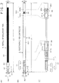
- FIG. 2 depicts diagrams showing a configuration example of the electronic pen cartridge 3 with comparison with a refill of a commercially-available knock-type ballpoint pen.
- FIG. 2(A) shows the refill 6 of the commercially-available knock-type ballpoint pen
- FIG. 2(B) shows a configuration example of the electronic pen cartridge 3 of the present embodiment.
- FIG. 2(C) is a diagram for explaining the configuration of the major parts of the electronic pen cartridge 3 of the present embodiment shown in FIG. 2(B) .
- the refill 6 of the commercially-available knock-type ballpoint pen has a well-known configuration in which a pen tip part 61 in which a ball is disposed at the tip and an ink storage 62 are joined at a joint part 63 and are integrated.
- the joint part 63 has the same diameter as the ink storage 62.
- the electronic pen cartridge 3 of the present embodiment has a configuration in which the core body unit 31 and a tubular body unit 32 are joined to be integrated as shown in FIG. 2(B) .
- the core body unit 31 has a configuration in which a coil 311 is wound partly around a magnetic core, specifically a ferrite core 310 in this example, and the part thereof around which the coil 311 is not wound is covered by a protective material 312 to form the pen tip part 313.
- the coil 311 is wound around a part with approximately half length of the total length of the ferrite core 310 from the vicinity of one end part of the ferrite core 310. Furthermore, in this example, the remaining part with approximately half length in the ferrite core 310, around which the coil 311 is not wound, is covered by the protective material 312 composed of e.g. a resin and is used as the pen tip part 313. As the protective material 312 of the pen tip part 313, a resin material that is comparatively hard and has elasticity, specifically e.g. polyoxymethylene (POM), is used.
- POM polyoxymethylene
- the configuration is so made that the diameter and length of the pen tip part 313 of the core body unit 31 of the electronic pen cartridge 3 are substantially equal to diameter R1 and length L1 of the pen tip part 61 of the refill 6 of the ballpoint pen. Furthermore, the configuration is so made that the diameter of the part around which the coil 311 is wound in the core body unit 31 of the electronic pen cartridge 3 is substantially equal to diameter R2 (R2 > R1) of the ink storage 62 of the refill 6 of the ballpoint pen.
- the tubular body unit 32 is composed of a first tubular body unit 321 in which electronic circuit components are disposed and a second tubular body unit 322 in which components for writing pressure detection are disposed.
- the length (total length) in the state in which the core body unit 31 and the tubular body unit 32 are joined is selected to be equal to total length L2 of the refill 6 of the ballpoint pen.
- a printed board 33 is disposed in the first tubular body unit 321 of the tubular body unit 32 as shown in FIG. 2(C) .
- an electronic circuit 34 including a capacitor that forms a resonant circuit with the coil 311, a memory that stores identification information (identification (ID)) forming part of additional information that should be sent out to a position detecting device when a user is carrying out position indication operation over the sensor by the electronic pen, an integrated circuit (IC), and so forth is provided.
- ID identification
- IC integrated circuit
- the core body unit 31 and the first tubular body unit 321 of the tubular body unit 32 are joined to be integrally configured in the state in which part of the ferrite core 310 of the core body unit 31 is inserted in the first tubular body unit 321 for example.
- a winding start end 311a and a winding finish end 311 b of the coil 311 are electrically connected to one end and the other end of the capacitor provided in the electronic circuit 34 in the first tubular body unit 321.
- the second tubular body unit 322 is formed of a tubular body with the diameter equal to the diameter R2 of the ink storage 62 of the refill 6 of the commercially-available ballpoint pen.
- the second tubular body unit 322 is divided into two parts of a longer part 322a and a shorter part 322b, and a writing pressure detecting member 36 is provided near a joint part 35 of them in this example.
- the longer part 322a and the shorter part 322b are joined at the joint part 35 with the intermediary of a linking bar member 351 and a coil spring 352 in this example.
- the coil spring 352 the longer part 322a and the shorter part 322b are always elastically displaced to be separated from each other in the axial center direction.
- the longer part 322a and the shorter part 322b are configured to be locked at predetermined positions by the linking bar member 351 so as not to be displaced in the axial center direction beyond the positions.
- the configuration is so made that the total length of the electronic pen cartridge 3 in the locked state is equal to the total length L2 of the refill 6 of the above-described ballpoint pen.
- the writing pressure detecting member 36 is provided in the longer part 322a in the present embodiment. Furthermore, the configuration is so made that the side of one end 351 a of the linking bar member 351 works as a pressing part of the writing pressure detecting member 36.
- the writing pressure detecting member 36 of this example can employ a configuration of a variable-capacitance capacitor that uses writing pressure detecting means with a well-known configuration described in a Patent Document: Japanese Patent Laid-Open No. 2011-186803 for example and whose capacitance changes according to the writing pressure. It is also possible to employ a configuration using a semiconductor element that allows the capacitance to vary according to the writing pressure like one disclosed in Japanese Patent Laid-Open No. 2013-161307 for example.
- the electronic pen cartridge 3 with the above configuration is housed in the chassis 2 by fitting the shorter part 322b of the tubular body unit 32 of the electronic pen cartridge 3 to the fitting part 43a of the rotary element 43 of the knock cam mechanism unit 4. In this state, the whole of the electronic pen cartridge 3 including the core body unit 31 thereof is housed in the chassis 2 and the core body unit 31 of the electronic pen cartridge 3 is protected.
- the user when using the electronic pen 1 with a position detecting device, the user presses down the end part 42a of the knock bar 42 to protrude the tip of the pen tip part 313 of the core body unit 31 from the opening 2b of the chassis 2 as shown in FIG. 1(B) . Thereby, the protection of the core body unit 31 of the electronic pen cartridge 3 is released. Then, when the use of the electronic pen 1 ends, the user presses down the end part 42a of the knock bar 42 again to house the whole of the electronic pen cartridge 3 in the hollow part 2a of the chassis 2 as shown in FIG. 1(A) and protect the core body unit 31.
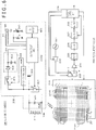
- FIG. 3 shows a circuit configuration example of the electronic circuit 34 of the electronic pen 1 and a circuit configuration example of a position detecting device 200 that carries signal transfer based on electromagnetic induction coupling with the electronic pen 1.
- the electronic pen 1 is configured to make electromagnetic induction coupling with conductors of a sensor of the position detecting device 200 to thereby transfer a signal for position detection and transmit, to the position detecting device 200, writing pressure information detected through the writing pressure detecting member 36 and identification information (ID) of the electronic pen 1 itself or identification information (ID) of the electronic pen cartridge 3.
- a capacitor 401 is connected in parallel to the coil 311 and a parallel resonant circuit 40R is formed.
- the electronic circuit 34 includes a control circuit 400 that controls transmission of additional information as shown in FIG. 3 .
- the control circuit 400 is formed as an IC.
- the IC that forms the control circuit 400 is configured to operate by a power supply Vcc obtained by rectifying an alternate current (AC) signal received in the parallel resonant circuit 40R from the position detecting device 200 by electromagnetic coupling in a rectifying circuit (power supply circuit) 404 composed of a diode 402 and a capacitor 403.
- Vcc obtained by rectifying an alternate current (AC) signal received in the parallel resonant circuit 40R from the position detecting device 200 by electromagnetic coupling in a rectifying circuit (power supply circuit) 404 composed of a diode 402 and a capacitor 403.
- a switch circuit 405 set to the open state normally (normal open) is provided between the parallel resonant circuit 40R and the power supply circuit 404.
- the switch circuit 405 is formed of a semiconductor switch circuit for example and is in the high-impedance state in the open state.
- the switch circuit 405 is controlled to be turned on by a switch control signal from a switch control circuit 406.
- the switch control circuit 406 generates the switch control signal from the AC signal received in the parallel resonant circuit 40R from the position detecting device 200 by electromagnetic coupling.
- a switch circuit 407 is connected in parallel to the parallel resonant circuit 40R composed of the coil 311 and the capacitor circuit 401.
- the switch circuit 407 is configured to be on/off-controlled by the control circuit 400.
- an electromagnetic induction signal transmitted from the position detecting device 200 is supplied through a capacitor 408 as a synchronization signal for transfer of the electromagnetic induction signal between the electronic pen 1 and the position detecting device 200.
- a variable-capacitance capacitor 36C formed of the writing pressure detecting member 36 is connected to the control circuit 400.
- a resistor R is connected in parallel to the variable-capacitance capacitor 36C.
- the control circuit 400 discharges the variable-capacitance capacitor 36C through the resistor R after charging the variable-capacitance capacitor 36C, and measures the time that elapses before the voltage of the terminal to which the variable-capacitance capacitor 36C is connected (equivalent to the voltage across the variable-capacitance capacitor 36C) becomes a predetermined threshold. Thereby, the control circuit 400 measures the capacitance of the variable-capacitance capacitor 36C.
- control circuit 400 detects change in the writing pressure from change in the measured capacitance of the variable-capacitance capacitor 36C and detects whether a writing pressure is applied to the electronic pen cartridge 3. In addition, when detecting that a writing pressure is applied, the control circuit 400 calculates the writing pressure value from the value of the capacitance of the variable-capacitance capacitor 36C.
- control circuit 400 transmits information on the calculated writing pressure value (writing pressure data) to the position detecting device 200 as a digital signal of plural bits by on/off-controlling the switch circuit 407.
- writing pressure data forms part of additional information.
- an ID memory 409 that stores identification information (ID) including the manufacturer number and product number of the electronic pen 1 or the electronic pen cartridge 3 is connected. Furthermore, the control circuit 400 reads out the identification information stored in the ID memory 409 and on/off-controls the switch circuit 407 to transmit the identification information to the position detecting device 200 as a digital signal of plural bits. In the present embodiment, this identification information also forms part of additional information.
- the control circuit 400 detects whether or not the tip of the pen tip part 313 of the core body unit 31 of the electronic pen cartridge 3 is protected, and carries out control to send out additional information only in the state in which the tip is not protected. In the present embodiment, the control circuit 400 detects whether or not the tip of the pen tip part 313 of the core body unit 31 of the electronic pen cartridge 3 is protected based on whether or not it is detected by the writing pressure detecting member 36 that a writing pressure is applied.
- the tip of the pen tip part 313 of the core body unit 31 of the electronic pen cartridge 3 does not protrude to the external and thus a writing pressure is not applied to the core body unit 31.
- the knock bar of the knock cam mechanism unit 4 has been operated and the protected state has been released, in which the tip of the pen tip part 313 of the core body unit 31 of the electronic pen cartridge 3 protrudes to the external from the opening 2b of the chassis 2, it is possible that a writing pressure is applied to the core body unit 31, and the state in which a writing pressure is actually applied is the state in which the electronic pen 1 is used by a user.
- the control circuit 400 detects it and determines that application of a writing pressure has been started.
- the writing pressure detecting means also has a function as detecting means for detecting whether or not the tip of the pen tip part 313 of the core body unit 31 of the electronic pen cartridge 3 is protected.
- the control circuit 400 when detecting that application of a writing pressure has not been started, the control circuit 400 always keeps the switch circuit 407 is in the off-state to provide the state in which the parallel resonant circuit 40R always works. Furthermore, when detecting that application of a writing pressure has been started, the control circuit 400 transmits writing pressure data and identification information to the position detecting device 200 as an amplitude shift keying (ASK) - modulated signal as described later by on/off-controlling the switch circuit 407 at timings based on the synchronization signal from the position detecting device received through the capacitor 408.
- the data and information may be modulated to an on off keying (OOK) signal instead of the ASK modulation.
- an X-axis direction loop coil group 211X and a Y-axis direction loop coil group 212Y are stacked and a position detecting coil is formed.
- the respective loop coil groups 211X and 212Y are composed of n and m, respectively, rectangular loop coils for example.
- the respective loop coils configuring the respective loop coil groups 211X and 212Y are disposed to be lined up at equal intervals and sequentially overlap with each other.
- a selection circuit 213 to which the X-axis direction loop coil group 211 X and the Y-axis direction loop coil group 212Y are connected is provided.
- the selection circuit 213 sequentially selects one loop coil in the two loop coil groups 211X and 212Y.
- the position detecting device 200 is provided with an oscillator 221, a current driver 222, a switching connecting circuit 223, a receiving amplifier 224, a detector 225, a low-pass filter 226, a sample/hold circuit 227, an analog to digital (A/D) conversion circuit 228, and a processing control unit 229.
- the processing control unit 229 is formed of a microcomputer for example.
- the oscillator 221 generates an AC signal with a frequency f0. Furthermore, the AC signal generated in the oscillator 221 is supplied to the current driver 222.
- the current driver 222 converts the AC signal supplied from the oscillator 221 to a current and sends out the current to the switching connecting circuit 223.
- the switching connecting circuit 223 switches the connection target (transmitting-side terminal T, receiving-side terminal R) to which the loop coil selected by the selection circuit 213 is connected. In these connection targets, the transmitting-side terminal T and the receiving-side terminal R are connected to the current driver 222 and the receiving amplifier 224, respectively.
- An induced voltage generated in the loop coil selected by the selection circuit 213 is sent to the receiving amplifier 224 via the selection circuit 213 and the switching connecting circuit 223.
- the receiving amplifier 224 amplifies the induced voltage supplied from the loop coil and sends out the amplified voltage to the detector 225.
- the detector 225 detects the induced voltage generated in the loop coil, i.e. the received signal, and sends out the received signal to the low-pass filter 226.
- the low-pass filter 226 has a cutoff frequency sufficiently lower than the above-described frequency f0 and converts the output signal of the detector 225 to a direct current (DC) signal to send out the DC signal to the sample/hold circuit 227.
- the sample/hold circuit 227 holds a voltage value at predetermined timing of the output signal of the low-pass filter 226, specifically at predetermined timing in the reception period, and sends out the voltage value to the A/D conversion circuit 228.
- the A/D conversion circuit 228 converts the analog output of the sample/hold circuit 227 to a digital signal and outputs the digital signal to the processing control unit 229.
- the processing control unit 229 controls selection of the loop coil in the selection circuit 213, switching by the switching connecting circuit 223, and the timing of the sample/hold circuit 227.
- the processing control unit 229 causes an electromagnetic induction signal to be transmitted from the X-axis direction loop coil group 211X and the Y-axis direction loop coil group 212Y with a certain transmission continuation time based on an input signal from the A/D conversion circuit 228.
- an induced voltage is generated by an electromagnetic induction signal transmitted from the electronic pen 1.
- the processing control unit 229 calculates the coordinate value of the position indicated by the electronic pen 1 in the X-axis direction and the Y-axis direction based on the level of the voltage value of this induced voltage generated in each loop coil.
- the processing control unit 229 supplies a signal for intermittence control of a transmission signal and a signal for control of the level of the transmission signal to the current driver 222 and executes reception processing of additional information such as writing pressure data and identification information from the electronic pen 1.
- the processing control unit 229 detects an intermittent signal formed of an ASK signal from the electronic pen 1 as a digital signal of plural bits and detects additional information such as writing pressure data and identification information.
- the position detecting device 200 sends out an AC signal of a transmission signal based on processing control of the processing control unit 229.
- the switch circuit 405 is in the off-state and the supply voltage Vcc is not supplied from the power supply circuit 404. In this state, the control circuit 400 stops operation and the switch circuit 407 is set to the off-state.
- the electronic pen 1 is in the state in which the AC signal from the position detecting device 200 can be received in the parallel resonant circuit 40R. Furthermore, when the electronic pen 1 is brought above the sensor of the position detecting device 200 by a user, the electronic pen 1 becomes the state in which the parallel resonant circuit 40R of the electronic pen 1 can receive the AC signal from the position detecting device 200 by electromagnetic induction coupling irrespective of whether or not the electronic pen cartridge 3 is in the protected state.
- the switch control circuit 406 of the electronic circuit 34 of the electronic pen 1 generates the switch control signal that turns on the switch circuit 405 from the AC signal received by the parallel resonant circuit 40R from the sensor of the position detecting device 200.
- the switch circuit 405 is turned on due to this, the supply voltage Vcc generated by rectifying the AC signal received by the parallel resonant circuit 40R is supplied from the power supply circuit 404 to the control circuit 400.
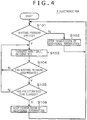
- FIG. 4 is a flowchart for explaining processing operation of the control circuit 400 of the electronic circuit 34 of the electronic pen 1.
- the control circuit 400 monitors change in the capacitance of the variable-capacitance capacitor 36C formed of the writing pressure detecting member 36 and determines whether or not a writing pressure is applied through the pen tip part 313 of the core body unit 31 of the electronic pen cartridge 3 (step S101).
- the control circuit 400 makes the state in which transmission of additional information is stopped and keeps the switch circuit 407 at the off-state constantly (step S102).
- the control circuit 400 returns the processing to the step S101 and repeats the processing of the step S101 and the subsequent steps.
- the state in which a writing pressure is applied is not obtained when the electronic pen cartridge 3 is all housed in the chassis 2 and is in the protected state.
- the state of the step S102 includes the time when the electronic pen cartridge 3 is in this protected state.
- the control circuit 400 When determining that a writing pressure is applied in the step S101, the control circuit 400 starts transmission of additional information (step S103). Specifically, the control circuit 400 calculates a writing pressure value from the measurement result of the capacitance of the variable-capacitance capacitor 36C formed of the writing pressure detecting member 36 and generates writing pressure data. Then, the control circuit 400 on/off-controls the switch circuit 407 according to the generated writing pressure data to thereby transmit the writing pressure data as part of the additional information from the electronic pen 1 to the position detecting device 200.
- the control circuit 400 reads out identification information of the electronic pen 1 or the electronic pen cartridge 3 from the ID memory 409 and on/off-controls the switch circuit 407 according to the read-out identification information to thereby transmit the identification information as part of the additional information from the electronic pen 1 to the position detecting device 200.
- the parallel resonant circuit 40R can carry out resonance operation in response to an AC signal transmitted from the position detecting device 200 and return an electromagnetic induction signal to the position detecting device 200.
- the loop coil of the position detecting device 200 receives the electromagnetic induction signal from the resonant circuit 40R of the electronic pen 1.
- the parallel resonant circuit 40R becomes the state in which the resonance operation in response to the AC signal from the position detecting device 200 is prohibited. For this reason, an electromagnetic induction signal is not returned from the parallel resonant circuit 40R to the position detecting device 200 and the loop coil of the position detecting device 200 does not receive the signal from the electronic pen 1.
- the processing control unit 229 of the position detecting device 200 carries out detection of whether or not a received signal from the electronic pen 1 is present the same number of times as the number of bits of additional information, and thereby receives the additional information of a digital signal of these plural bits.
- the control circuit 400 of the electronic pen 1 generates a digital signal of plural bits corresponding to additional information to be transmitted and on/off-controls the switch circuit 407 in synchronization with transmission and reception of an electromagnetic induction signal between the electronic pen 1 and the position detecting device 200 based on the digital signal of the plural bits.
- the switch circuit 407 is turned on when the bit of the additional information is "1.” In this case, an electromagnetic induction signal is not returned from the electronic pen 1 to the position detecting device 200 as described above.
- the switch circuit 407 is turned off. In this case, an electromagnetic induction signal is returned from the electronic pen 1 to the position detecting device 200 as described above.
- the processing control unit 229 of the position detecting device 200 can receive the additional information that is a digital signal by carrying out detection of whether or not a received signal from the electronic pen 1 is present the same number of times as the number of bits of the additional information.
- control circuit 400 monitors change in the writing pressure based on the capacitance of the variable-capacitance capacitor 36C formed of the writing pressure detecting member 36 and determines whether or not the writing pressure has come not to be applied and disappeared (step S104). When determining in the step S104 that the writing pressure is applied and has not disappeared, the control circuit 400 returns the processing to the step S103 and repeats the processing of the step S103 and the subsequent steps.
- the control circuit 400 determines whether or not the disappearance state of the writing pressure has continued for a predetermined time or longer, specifically for 10 seconds or longer for example (step S105). When determining that the predetermined time or longer has not elapsed, the control circuit 400 returns the processing to the step S103 and repeats the processing of the step S103 and the subsequent steps. When determining in the step S105 that the disappearance state of the writing pressure has continued for the predetermined time or longer, the control circuit 400 stops the transmission of the additional information (step S106) and intends protection of security of the additional information. Subsequently to the step S106, the control circuit 400 returns the processing to the step S101 and repeats the processing of the step S101 and the subsequent steps.
- That the transmission of the additional information is not immediately stopped when it is determined that the writing pressure has come not to be applied and disappeared in the step S104 is based on consideration of the case in which the user temporarily separates the electronic pen 1 from the sensor surface of the position detecting device 200 although continuing input with the sensor surface by the electronic pen 1.
- the electronic pen cartridge 3 can be housed in the chassis 2 by the knock cam mechanism unit and the tip of the pen tip part 313 of the core body unit 31 of the electronic pen cartridge 3 can be protruded from the opening of the chassis 2 by operating the knock bar according to need.
- the tip of the pen tip part 313 of the core body unit 31 of the electronic pen cartridge 3 is housed in the chassis 2 and thereby can be set to the protected state. Specifically, in this protected state, the tip of the pen tip part 313 of the core body unit 31 does not protrude to the external. Thus, even when the electronic pen 1 is accidentally dropped, the core body unit 31 of the electronic pen cartridge 3 does not directly receive the shock of the drop and is protected.
- the additional information such as the identification information of the electronic pen 1 or the electronic pen cartridge 3 is not transmitted to the position detecting device 200 and security of the additional information can be ensured.
- the state in which the electronic pen cartridge 3 is protected is not the state in which the electronic pen 1 is used by the user.
- this state in which transmission of the additional information is stopped also provides an effect that useless signal transmitting can be avoided and the additional information can be transmitted to the position detecting device only when necessary.
- control is carried out to cause the additional information to be sent out to the position detecting device 200. Therefore, according to the electronic pen 1 of the present embodiment, the necessary additional information is sent out to the position detecting device 200 only in the practical used state by the user. Thus, there is an effect that the transmission of the additional information for which ensuring of security is necessary can be kept to the minimum necessary.
- the problem of ensuring of security of the additional information and avoidance of unnecessary transmission and the problem of protection of the core body can be simultaneously solved.
- the tubular body unit 32 by making the tubular body unit 32 have a thin shape in addition to the core body unit 31, thickness reduction of the whole of the electronic pen cartridge 3 is enabled. This can realize thickness reduction of the electronic pen 1.
- the electronic pen cartridge 3 it becomes possible to enable the electronic pen cartridge 3 to have a configuration that allows ensuring of compatibility with a refill of a commercially-available ballpoint pen as in the above-described embodiment.
- the electronic pen cartridge 3 has the configuration that allows ensuring of compatibility with a refill of a commercially-available ballpoint pen, there is a merit that the chassis of the commercially-available ballpoint pen can be diverted as the chassis 2 of the electronic pen 1. That is, the electronic pen 1 can be configured by housing the electronic pen cartridge 3 of the present embodiment instead of a refill of the ballpoint pen in the chassis of the ballpoint pen.
- the method for the switch control circuit 406 of the electronic circuit 34 of the electronic pen 1 to turn on the switch circuit 405 to provide the power supply Vcc to the control circuit 400 is not limited to the above-described method.
- the electronic pen cartridge is provided with the writing pressure detecting member and a threshold is set regarding the pressure detected by the writing pressure detecting member. Furthermore, it is detected that the tip of the pen tip part 313 is protected when the pressure detected by the writing pressure detecting member surpasses the threshold.
- a switch that is turned on according to the pressure applied to the electronic pen cartridge may be provided instead of the writing pressure detecting member, and it may be detected that at least the tip of the pen tip part 313 of the core body unit 31 is protected when this switch is turned on.
- An electronic pen of the second embodiment is a modification example of the first embodiment.
- only one electronic pen cartridge is housed in the chassis.
- plural electronic pen cartridges are housed in the chassis.
- one of the plural electronic pen cartridges is selected by a knock mechanism and the tip of the pen tip part of the selected electronic pen cartridge is protruded from an opening of the chassis on the pen tip side and is used.
- the electronic pen cartridge 3 of the electronic pen 1 of the first embodiment has a configuration that ensures compatibility with the refill 6 of a ballpoint pen.
- a multicolor ballpoint pen in which refills with different ink colors are mounted exists.
- the second embodiment provides an electronic pen configured by housing the electronic pen cartridges 3 in a chassis with a configuration similar to that of the chassis of this multicolor ballpoint pen.
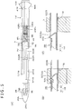
- FIG. 5(A) is a configuration diagram showing the appearance of an electronic pen 1M of the second embodiment. This example of FIG. 5(A) is also shown as the state in which a chassis 2M of the electronic pen 1M is composed of a transparent synthetic resin and the inside thereof is see-through.
- the chassis 2M of the electronic pen 1M has the same configuration as the chassis and knock mechanism of a commercially-available knock-type multicolor ballpoint pen.
- the chassis and knock mechanism of a commercially-available knock-type multicolor ballpoint pen may be used as they are.
- three electronic pen cartridges 3B, 3R, and 3E are housed in the chassis 2M.
- An opening 2Ma is formed on one end side of the chassis 2M in the axial center direction.
- the whole of the electronic pen cartridges 3B, 3R, and 3E including the tips of the pen tip parts 313 of the respective core body units 31 is housed in the hollow part of the chassis 2M and is in the protected state as shown in FIG. 5(A) .
- the tip of the pen tip part 313 of the core body unit 31 of the electronic pen cartridge slide-moved in the axial center direction by the knock mechanism in the electronic pen cartridges 3B, 3R, and 3E is caused to protrude to the external through the opening 2Ma. Therefore, the above-described protection is released in the electronic pen cartridge whose tip of the pen tip part 313 of the core body unit 31 is caused to protrude to the external through the opening 2Ma by the knock mechanism.
- These electronic pen cartridges 3B, 3R, and 3E are configured similarly to the electronic pen cartridge 3 of the first embodiment in terms of the outer shape except for that the electronic pen cartridges 3B, 3R, and 3E are formed with the same dimensions as refills of the multicolor ballpoint pen.
- the second tubular body unit 322 is provided with a switch member that is turned on and off according to movement in the axial center direction by the knock mechanism as described later.
- the electronic pen 1M of the second embodiment As described later, based on the state of the switches provided in these electronic pen cartridges 3B, 3R, and 3E, it is detected whether the respective electronic pen cartridges 3B, 3R, and 3E are set to the protected state by the knock mechanism in the electronic pen 1M.
- the other configurations of the electronic pen cartridges 3B, 3R, and 3E are set similarly to the electronic pen cartridge 3 of the first embodiment.
- the knock mechanism of the electronic pen 1M is composed of knock bars 42B, 42R, and 42E having fitting parts 42Ba, 42Ra, and 42Ea to which a respective one of the electronic pen cartridges 3B, 3R, and 3E is fitted, a spring receiving member 7, and coil springs 8B, 8R, and 8E disposed between the fitting parts 42Ba, 42Ra, and 42Ea of a respective one of the electronic pen cartridges 3B, 3R, and 3E and the spring receiving member 7.
- the spring receiving member 7 is attached to be fixed at a predetermined position in the axial center direction in the hollow part of the chassis 2M.
- through-holes 7B, 7R, and 7E in which second tubular body units 322B, 322R, and 322E of the electronic pen cartridges 3B, 3R, and 3E are inserted are formed.
- Each of the electronic pen cartridges 3B, 3R, and 3E is attached to the electronic pen 1M by being inserted in a respective one of the through-holes 7B, 7R, and 7E of the spring receiving member 7 and a respective one of the coil springs 8B, 8R, and 8E and being fitted to the fitting parts 42Ba, 42Ra, and 42Ea of the knock bars 42B, 42R, and 42E.
- through-hole slits (diagrammatic representation is omitted in FIG. 5(A) ) through which part of the knock bars 42B, 42R, and 42E is exposed to the outside and by which each of the knock bars 42B, 42R, and 42E is enabled to move in the axial center direction are made.
- the electronic pen 1M As with a well-known multicolor ballpoint pen, when any of the knock bars 42B, 42R, and 42E is slid to the side of the opening 2Ma and the electronic pen 1M becomes the state in which the tip of the pen tip part 313 of the core body unit 31 of any of the electronic pen cartridges 3B, 3R, and 3E fitted to the knock bar protrudes from the opening 2Ma to the external, a locking part (diagrammatic representation is omitted) of the knock bar 42B, 42R, or 42E engages with an engagement part formed in the hollow part of the chassis 2M and the knock bar becomes the locked state in which the locking part is locked in the state.
- a locking part (diagrammatic representation is omitted) of the knock bar 42B, 42R, or 42E engages with an engagement part formed in the hollow part of the chassis 2M and the knock bar becomes the locked state in which the locking part is locked in the state.
- the electronic pen cartridge whose tip is protruded from the opening 2Ma can be changed by slide-moving the knock bar similarly.
- slide movement of any of the knock bars 42B, 42R, and 42E is stopped in the middle of becoming the locked state, lock release of another knock bar that is currently locked is carried out and the knock bar returns to the protected state of FIG. 5(A) due to any of the coil springs 8B, 8R, and 8E.
- FIGS. 5(B) and 5(C) are diagrams for explaining the switches provided in the electronic pen cartridges 3B, 3R, and 3E. These FIGS. 5(B) and 5(C) show the switch provided in the electronic pen cartridge 3B and the switch is similarly configured also regarding the other electronic pen cartridges 3R and 3E.
- a through-hole 322Ba is set just in the circumferential surface of the part of the second tubular body unit 322B housed in the through-hole 7B of the spring receiving member 7.
- a switch member 9B is provided in such a manner that part thereof is exposed from the through-hole 322Ba.
- the switch member 9B is composed of a material having elasticity and having electrical conductivity, specifically an electrically-conductive metal having elasticity for example. As shown in FIGS. 5(B) and 5(C) , the switch member 9B is composed of a fixed terminal piece 91 fixed to the inner wall surface near the through-hole 322Ba of the second tubular body unit 322B and a movable terminal piece 92 that can be elastically in contact with this fixed terminal piece 91.
- the movable terminal piece 92 includes a bent part 92a configured to be capable of assuming the state of being elastically in contact with the fixed terminal piece 91 and the non-contact state, and is attached to the inside of the second tubular body unit 322B in such a manner that part of the bent part 92a can protrude from the through-hole 322Ba.
- the switch member 9B When the electronic pen cartridge 3B is fitted to the fitting part 42Ba of the knock bar 42B in the non-locked state and is in the protected state in which the whole of the electronic pen cartridge 3B exists in the hollow part of the chassis 2M, the switch member 9B is located just in the through-hole 7B of the spring receiving member 7 as shown in FIG. 5(B) .
- the bent part 92a of the movable terminal piece 92 is elastically displaced to the inside of the second tubular body unit 322B due to the inner wall of the through-hole 7B, which provides the state in which the fixed terminal piece 91 and the movable terminal piece 92 are not in contact with but separated from each other. That is, the switch member 9B is in the off-state.
- the switch member 9B becomes the state of being out of the through-hole 7B of the spring receiving member 7 as shown in FIG. 5(C) .
- part of the bent part 92a of the movable terminal piece 92 is elastically displaced to protrude from the through-hole 322Ba, which provides the state in which the movable terminal piece 92 and the fixed terminal piece 91 are in contact with each other. That is, the switch member 9B becomes the on-state.
- the fixed terminal piece 9a and the movable terminal piece 9b of the switch member 9B are electrically connected to a control circuit 400B of an electronic circuit 34B housed in a first tubular body unit 321B.
- the control circuit 400 monitors the on/off-state of the switch member 9B to thereby detect whether the electronic pen cartridge 3B is in the protected state in which the whole of the electronic pen cartridge 3B exists in the hollow part of the chassis 2M or in the unprotected state in which the tip of the pen tip part 313 of the core body unit 31 of the electronic pen cartridge 3B protrudes from the opening 2Ma of the chassis 2M by the knock bar 42B.
- switch members 9R and 9E are provided in the second tubular body unit 322R and are connected to control circuits 400R and 400E (diagrammatic representation is omitted) of electronic circuits 34R and 34E (diagrammatic representation is omitted) housed in first tubular body units 321R and 321E.
- FIG. 6 shows the relationship between the electronic pen cartridge 3B in the electronic pen 1M and the position detecting device 200, it goes without saying that the relationship between the electronic pen cartridges 3R and 3E of the electronic pen 1M and the position detecting device 200 is also similar.
- the position detecting device used with the electronic pen cartridges 3B, 3R, and 3E has a function of receiving and discriminating identification information transmitted from each of the electronic pen cartridges 3B, 3R, and 3E. That is, the position detecting device of the case of the present embodiment discriminates the difference among the electronic pen cartridges 3B, 3R, and 3E and implements the functions assigned to a respective one of the electronic pen cartridges 3B, 3R, and 3E.
- a function of representing a locus (character or graphic) displayed according to the indicated position thereof by black is assigned to the electronic pen cartridge 3B.
- a function of representing a locus displayed according to the indicated position thereof by red is assigned.
- a function of erasing a locus indicated and input previously according to the indicated position thereof is assigned.
- information to notify these character colors and information to notify the erasure function are stored besides the identification information of the electronic pen 1M and the electronic pen cartridges 3B, 3R, and 3E.
- the information to notify these character colors and information to notify the erasure function are included besides the identification information of the electronic pen 1M and the electronic pen cartridges 3B, 3R, and 3E.
- the function assigned to the electronic pen cartridge may be not only the display color of the locus according to the indicated position as in this example but the thickness of the locus, the type of line displayed, such as a solid line, a dotted line, or a one-dot chain line, and so forth.
- FIG. 7 is a flowchart for explaining processing operation of transmission control of additional information in the control circuit 400B of the electronic circuit 34B of the electronic pen cartridge 3B.
- the control circuit 400B determines whether or not the switch member 9B has been turned on by knock operation (slide movement operation) of the knock bar 42B by a user (step S201). When determining that the switch member 9B is not in the on-state but in the off-state in the step S201, the control circuit 400B deems that the electronic pen cartridge 3B is all housed in the chassis 2M and is in the protected state, and makes the state in which transmission of additional information is stopped and keeps the switch circuit 407 at the off-state constantly (step S202). After the step S202, the control circuit 400B returns the processing to the step S201 and repeats the processing of the step S201 and the subsequent steps.
- the control circuit 400B determines that knock operation (slide movement operation) of the knock bar 42B has been carried out by the user and the tip of the pen tip part 313 of the core body unit 31 of the electronic pen cartridge 3B is in the unprotected state in which the tip protrudes from the opening 2b of the chassis 2, and starts transmission of additional information (step S203).
- control circuit 400B transmits writing pressure data to the position detecting device 200 as the additional information. Furthermore, the control circuit 400B reads out the identification information of the electronic pen 1 or the electronic pen cartridge 3 and information to notify the character color from the ID memory 409 and transmits the read-out identification information and information to notify the character color to the position detecting device 200 as the additional information. In the case of the electronic pen cartridge 3E, the erasure function is notified instead of the notification of the character color.
- control circuit 400B determines whether or not the switch member 9B has been turned off (step S204). When determining that the switch member 9B has not been turned off, the control circuit 400B returns the processing to the step S203 and repeats the processing of the step S203 and the subsequent steps.
- the control circuit 400B determines that the electronic pen cartridge 3B has returned to the protected state in which the whole of the electronic pen cartridge 3B is housed in the hollow part of the chassis 2M by knock operation of the knock bar 42R or 42E of another electronic pen cartridge 3R or 3B, and stops the transmission of the additional information (step S205) to intend protection of security of the additional information. Subsequently to the step S205, the control circuit 400B returns the processing to the step S201 and repeats the processing of the step S201 and the subsequent steps.
- the problem of ensuring of security of the additional information and the problem of protection of the core body can be simultaneously solved also in the state in which plural electronic pen cartridges are housed in one chassis 2M.
- the switch members 9B, 9R, and 9E are used as detecting means that detects the protected state and the unprotected state according to slide movement of the electronic pen cartridges 3B, 3R, and 3E in the axial center direction by the knock mechanism.
- the detecting means is not limited thereto.
- optical sensors may be provided at corresponding positions on the second tubular body unit.
- the optical sensors when the electronic pen cartridges 3B, 3R, and 3E are in the protected state, the optical sensors are located in the through-holes 7B, 7R, and 7E of the spring receiving member 7 and are in such a state as not to receive light.
- the optical sensors when the electronic pen cartridges 3B, 3R, and 3E become the unprotected state, the optical sensors are located outside the through-holes 7B, 7R, and 7E of the spring receiving member 7 and become the state of being capable of receiving light through the transparent chassis 2M. Therefore, each of the control circuit 400B, 400R, and 400E can detect whether the electronic pen cartridge 3B, 3R, or 3E is in the protected state or in the unprotected state by monitoring the level of the light reception output of the optical sensor.
- the electronic pens 1 and 1M of the above-described first embodiment and second embodiment are the case of the electromagnetic induction coupling system in which transfer of a signal for position detection and additional information is carried out with the position detecting device 200 by electromagnetic induction coupling.
- the electronic pen of the present invention is not limited to the electronic pen of the electromagnetic induction coupling system and may be an electronic pen of the capacitive coupling system that carries out transfer of signals with a position detecting device by capacitive coupling.
- a third embodiment is an example of an electronic pen of this capacitive coupling system and is an example of a transmission-type electronic pen.
- FIG. 8 shows the outline of the mechanical configuration of an electronic pen 1C of the third embodiment.
- the electronic pen 1C of this example is composed of an electronic pen main body 1 Ca and a cap 1Cb that engages with this electronic pen main body in such a manner as to cover the side of a core body 506 serving as the pen tip of the electronic pen main body 1Ca.
- a diagram is made by breaking part of the electronic pen main body 1 Ca and the cap 1Cb and showing the inside thereof.
- an enlarged sectional view for explaining the internal configuration of the part on the pen tip side of the electronic pen main body 1Ca, which is not broken in FIG. 8 is shown in FIG. 9 .
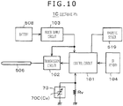
- FIG. 10 is a diagram showing an internal circuit configuration example of the electronic pen 1C.
- the electronic pen main body 1Ca includes a case 501 that forms a chassis formed into a circular tubular shape elongated in the axial center direction.
- the case 501 is composed of a case main body 502 composed of an electrically-conductive material, a pen tip sleeve 503 that is joined to the case main body 502 and is composed of an electrically-conductive material, and a lid portion 504 composed of a non-electrically-conductive material.
- a pen tip guard member 505 composed of an insulating material is fitted and provided.
- the core body 506 is composed of an electrically-conductive material, specifically a resin into which metal powders are mixed in this example. As shown in FIG. 9 , the core body 506 is inserted into a through-hole 505a of the pen tip guard member 505 from an opening 501a in the state of being freely movable in the axial center direction.
- a board holder 507 In the hollow part of the case main body 50, a board holder 507, a battery 508, and a core body holder 509 are housed as shown in FIGS. 8 and 9 .
- the board holder 507 is composed of an insulating resin, specifically a liquid crystal polymer for example, and includes a holding part (hereinafter, referred to as holding part for components for pressure sensing) 507a for a writing pressure detecting module 70 as an example of pressure detecting means and a printed board placement base 507b.
- the position of the board holder 507 is restricted so that the board holder 507 may be prevented from moving to the side of the core body 506 in the axial center direction in the case main body 502.
- a terminal conductor 510 that electrically abuts against a positive terminal 508a of the battery 508 is provided at the end part of the printed board placement base 507b on the side of the lid portion 504.
- the terminal conductor 510 is electrically connected to a copper foil pattern of a power supply line of a printed board 511.
- a coil spring terminal 512 composed of an electrically-conductive metal that is electrically connected to a negative terminal 508b of the battery 508 and is connected to an earth conductor of the printed board 511 is provided.
- the earth conductor of the printed board 511 is not connected to the case main body 502 and the pen tip sleeve 503.
- a transmission circuit 102 that generates a signal to be sent out from the core body 506 of the electronic pen 1C, a control circuit 101 that controls activation and the transmission operation state of this transmission circuit 102, a power supply circuit 103, and so forth, and peripheral circuit components thereof are provided.
- the core body holder 509 is composed of an electrically-conductive material and has a shape in which a housing fitting part 509a in which an electrically-conductive elastic member 513 composed of e.g. electrically-conductive rubber is fitted and housed and a bar-shaped part 509b fitted to the writing pressure detecting module 70 are monolithically formed.
- the core body 506 is fitted to and held by the core body holder 509 with the intermediary of the electrically-conductive elastic member 513 but is configured to be capable of being withdrawn from the core body holder 509 through pulling by a predetermined force.
- the bar-shaped part 509b of the core body holder 509 is fitted to a holding member 73 to be described later in the writing pressure detecting module 70 in the holding part 507a for components for pressure sensing in the board holder 507.
- a coil spring 515 composed of an electrically-conductive material such as an electrically-conductive metal is mounted on the bar-shaped part 509b of the core body holder 509 and the core body holder 509 is configured to be always biased to the side of the core body 506 relative to the board holder 507 by the coil spring 515.
- a member for an electrical connection is formed by a conductor terminal member 516 provided to straddle the holding part 507a for components for pressure sensing and the coil spring 515 composed of an electrically-conductive material.
- a conductor terminal member 516 provided to straddle the holding part 507a for components for pressure sensing and the coil spring 515 composed of an electrically-conductive material.
- the conductor terminal member 516 is composed of an abutting plate part 516a against which one end of the coil spring 515 abuts and an extending part 516b for connecting this abutting plate part 516a and a copper foil part connected to a signal supply terminal of the transmission circuit 102 of the printed board placement base 507b across the part of the holding part 507a for components for pressure sensing in the board holder 507.
- a signal from the transmission circuit 102 is supplied to the core body 506 inserted and fitted into the electrically-conductive elastic member 513 via the conductor terminal member 516, the coil spring 515, the core body holder 509, and the electrically-conductive elastic member 513.
- the writing pressure detecting module 70 of this example is provided with a configuration of a variable-capacitance capacitor whose capacitance changes according to the writing pressure applied to the core body 506.
- the writing pressure detecting module 70 in the present embodiment is formed by using a well-known variable-capacitance capacitor described in Japanese Patent Laid-Open No. 2011-186803 for example.
- Components for pressure sensing that form the writing pressure detecting module 70 of this example are composed of plural components, a dielectric 71, a terminal member 72, the holding member 73, an electrically-conductive member 74, and an elastic member 75, as shown in FIG. 9 . These components for pressure sensing that form the writing pressure detecting module 70 are lined up in the axial center direction and are housed in the hollow part of a tubular body 517 of the holding part 507a for components for pressure sensing in the board holder 507.
- variable-capacitance capacitor formed as the writing pressure detecting module 70 of this example is formed through sandwiching of the dielectric 71 between the terminal member 72 that forms one electrode of the variable-capacitance capacitor and the electrically-conductive member 74 that forms the other electrode.
- the terminal member 72 and the electrically-conductive member 74 are connected to the copper foil pattern of the printed board 511 across a wall part.
- the holding member 73 that holds the electrically-conductive member 74 is configured to be movable in the axial center direction in the tubular body 517. Moreover, the holding member 73 is always biased to the core body side by the elastic member 75 formed of a coil spring composed of an electrically-conductive material.
- the electrically-conductive member 74 is electrically connected to the elastic member 75 and one end 75a of the coil spring that forms the elastic member 75 is connected to the copper foil pattern of the printed board 511 as the other electrode of the variable-capacitance capacitor.
- a recess 73a is made on the side as the side of the core body 506 in the axial center direction thereof as shown in FIG. 9 .
- the bar-shaped part 509b of the core body holder 509 is press-fitted into the recess 73a of the member 73 and is engaged so as not to fall off to the side of the core body 506.
- the core body 506 and the core body holder 509 are displaced to the side of the lid portion 504 in the axial center direction according to the pressure. Due to this displacement, the holding member 73 in the holding part 507a for components for pressure sensing is displaced to the side of the dielectric 71 against the elastic biasing force of the elastic member 75. As a result, the electrically-conductive member 74 fitted to the holding member 73 is displaced to the side of the dielectric 71, so that the distance between the electrically-conductive member 74 and the dielectric 71 and the contact area between the electrically-conductive member 74 and the dielectric 71 change according to the pressure applied to the core body 506. Due to this, the capacitance of the variable-capacitance capacitor that forms the writing pressure detecting module 70 changes according to the pressure applied to the core body 506, so that the change in the capacitance is detected by the control circuit 101 and the writing pressure is detected.
- the cap 1Cb is put on the side of the core body 506 of the electronic pen main body 1 Ca and thereby the tip of the core body 506 protruding from the opening 501a of the case 501 of the electronic pen main body 1Ca is protected. That is, in the third embodiment, the cap 1Cb works as a protection mechanism for the core body 506 protruding from the opening 501a of the electronic pen main body 1Ca.
- the cap 1Cb becomes the state of being locked to the case 501 by screwing to the case 501 of the electronic pen main body 1Ca.
- a screw part 521 is made on the inner wall surface of a hollow part 520 of the cap 1 Cb.
- a screw part 518 that screws to the screw part 521 of the cap 1Cb is formed in the case main body 502 of the electronic pen main body 1Ca.
- the cap 1Cb and the case main body 502 are provided with a permanent magnet 522 and a magnetic sensor 519, respectively, at positions that become the state of being opposed to each other when the cap 1 Cb screws to the case main body 502.
- the magnetic sensor 519 that detects magnetic flux from the permanent magnet 522 forms detecting means about whether or not the tip of the core body of the electronic pen 1C is protected.
- the magnetic flux from the permanent magnet 522 provided in the cap 1Cb is detected by the magnetic sensor provided in the case main body 502 and it is detected that the core body 506 is in the protected state. Furthermore, in the state in which the cap 1 Cb is released from the joining to the case main body 502 and the core body 506 is exposed to the external, the magnetic flux from the permanent magnet 522 of the cap 1Cb cannot be detected in the magnetic sensor 519 and thus it can be detected that the core body 506 is in the unprotected state based on the output of the magnetic sensor 519 at the time.
- the magnetic sensor 519 is electrically connected to an electrically-conductive pattern of the printed board 511. Specifically, as shown in FIG. 10 , the magnetic sensor 519 is connected to the control circuit 101 provided on the printed board 511.
- FIG. 10 is a block diagram showing the configuration of an electronic circuit of the major part of the electronic pen 1C of the third embodiment, centered around the above-described control circuit 101 and transmission circuit 102.
- the battery 508 is connected to the power supply circuit 103.
- the supply voltage of the transmission-type electronic pen 1C of the present embodiment is generated and is supplied to the control circuit 101 and the transmission circuit 102.
- the control circuit 101 is formed as an IC.
- the transmission circuit 102 internally includes an oscillator (diagrammatic representation is omitted) in this example and generates and outputs a transmission signal based on an oscillation signal from this oscillator.
- the transmission signal from the transmission circuit 102 is supplied to the core body 506, which is an electrical conductor, and this transmission signal is transmitted to the position detecting device 200C through the core body 506.
- the control circuit 101 is formed of a microcomputer in this example and controls activation of the transmission operation of the transmission circuit 102 and controls the transmission operation state thereof. In this control of the transmission operation state, amplitude control of the oscillation signal from the oscillator included in the transmission circuit 102, control of the intermittence of the oscillation signal, and so forth are included.
- control circuit 101 monitors capacitance Cv of a variable-capacitance capacitor 70C formed of the writing pressure detecting module 70 and detects the value of the writing pressure applied to the core body 506 from the capacitance Cv of the variable-capacitance capacitor 70C similarly to the above-described embodiments.
- an ID memory 104 that stores identification information (ID) of the electronic pen 1C is connected and the magnetic sensor 519 is connected as described above.
- the control circuit 101 monitors the sensor output of the magnetic sensor 519 and determines whether or not the core body 506 is in the state of being protected by the cap 1Cb.
- the control circuit 101 when determining that the core body 506 is in the state of being protected by the cap 1 Cb from the sensor output of the magnetic sensor 519, the control circuit 101 carries out control to keep additional information composed of writing pressure data and the identification information in the ID memory 104 from being sent out to the position detecting device 200C.
- the control circuit 101 calculates writing pressure data and reads out the identification information from the ID memory 104 and carries out control to send out additional information composed of them to the position detecting device 200C.
- control circuit 101 determines whether or not the core body 506 is in the state of being protected by the cap 1Cb from the sensor output of the magnetic sensor 519 instead of detecting the on-state or off-state of the switch members 9B, 9R, and 9E.
- the control circuit 101 does not only stop the transmission of additional information but turns the transmission of the transmission signal from the transmission circuit 102 to the stopped state to alleviate battery consumption of the battery 508 as much as possible when determining that the core body 506 is in the protected state.
- the position detecting device 200C that receives a signal from the electronic pen 1C in the third embodiment is composed of a sensor 230 and a pen indication detecting circuit 240 connected to the sensor 230.
- the sensor 23 of the position detecting device 200C of this example has a configuration to receive a signal sent out from the transmission-type electronic pen 1C and detect the position indicated by the electronic pen 1C and receive additional information by using a sensor pattern formed by making a group of first conductors and a group of second conductors intersect.
- the group of first conductors is a group obtained by disposing plural first conductors 231Y 1 , 231Y 2 , ⁇ , 231Y m (m is an integer equal to or larger than 1) that extend along the horizontal direction (X-axis direction) in the Y-axis direction in parallel, with the plural first conductors 231Y 1 , 231Y 2 , ⁇ , 231Y m separated from each other by predetermined intervals.
- the group of second conductors is a group obtained by disposing plural second conductors 232X 1 , 232X 2 , ⁇ , 232X n (n is an integer equal to or larger than 1) that extend along a direction intersecting the extension direction of the first conductors 231Y 1 , 231Y 2 , ⁇ , 231Y m , specifically the vertical direction (Y-axis direction) orthogonal to the extension direction in this example, in the X-axis direction in parallel, with the plural second conductors 232X 1 , 232X 2 , ⁇ , 232X n separated from each other by predetermined intervals.
- the conductor will be referred to as the first conductor 231Y when there is no need to discriminate the respective conductors.
- the conductor will be referred to as the second conductor 232X when there is no need to discriminate the respective conductors.
- the pen indication detecting circuit 240 is composed of a selection circuit 241 used as an input/output interface with the sensor 230, an amplifying circuit 242, a band-pass filter 243, a detection circuit 244, a sample/hold circuit 245, an AD conversion circuit 246, and a control circuit 247.
- the selection circuit 241 selects one conductor from each of the group of first conductors and the group of second conductors based on a control signal from the control circuit 247.
- the conductors selected by the selection circuit 241 are connected to the amplifying circuit 242 and a signal from the electronic pen 1C is detected by the selected conductors and is amplified by the amplifying circuit 242.
- the output of the amplifying circuit 242 is supplied to the band-pass filter 243 and only a component of the frequency of the signal transmitted from the electronic pen 1C is extracted.
- An output signal of the band-pass filter 243 is subjected to detection by the detection circuit 244.
- An output signal of the detection circuit 244 is supplied to the sample/hold circuit 245 and is sampled and held at predetermined timing based on a sampling signal from the control circuit 247. Thereafter, the signal is converted to a digital value by the AD conversion circuit 246.
- the digital data from the AD conversion circuit 246 is read by the control circuit 247 and is processed.
- the control circuit 247 operates to send out a control signal to each of the sample/hold circuit 245, the AD conversion circuit 246, and the selection circuit 241 based on a program stored in a read-only memory (ROM) inside the control circuit 247. Furthermore, the control circuit 247 calculates position coordinates on the sensor 230 indicated by the electronic pen 1C from the digital data from the AD conversion circuit 246. Moreover, the control circuit 247 demodulates additional information sent from the electronic pen 1C from the digital data from the AD conversion circuit 246.
- ROM read-only memory
- FIG. 12 depicts timing chart for explaining a signal of a predetermined pattern from the transmission-type electronic pen 1C of the present embodiment, received by the sensor 230 of the position detecting device 200C.
- the control circuit 101 determines whether or not the core body 506 is in the state of being protected by the cap 1Cb based on the sensor output of the magnetic sensor 519, and repeatedly outputs the signal of the predetermined pattern composed of a signal for position detection and additional information from the transmission circuit 102 when determining that the core body 506 is in the unprotected state.
- the additional information is composed of writing pressure data calculated from the capacitance of the variable-capacitance capacitor 70C formed of the writing pressure detecting module 70 and the identification information of the electronic pen 1C read out from the ID memory 104.
- FIG. 12(A) shows an example of the control signal from the control circuit 101.
- the transmission signal from the transmission circuit 102 is continuously transmitted as a burst signal (continuous transmission period in FIG. 12(C) ).
- the length of this continuous transmission period is set to time length with which an indicated position on the sensor 230 by the electronic pen 1C can be detected in the pen indication detecting circuit 240 of the position detecting device 200C.
- the length is set to time length with which all of the first conductors 231Y and the second conductors 232X can be scanned one or more times, preferably plural times.
- the control circuit 101 detects the value of the writing pressure applied to the core body 506 as a value according to the capacitance of the variable-capacitance capacitor 70C formed of the writing pressure detecting module 70 by a method similar to that described in the first embodiment, and obtains the writing pressure value as a value of plural bits, specifically 10 bits for example (binary code).
- the control circuit 101 carries out ASK modulation of the transmission signal from the transmission circuit 102 by controlling the control signal to the high level or low level at a predetermined cycle (Td).
- the control circuit 101 invariably sets the control signal to the high level in the first round of the predetermined cycle (Td) and employs it as a start signal in FIG. 12(C) .
- This start signal is a timing signal for allowing the subsequent data transmission timing to be accurately determined on the side of the position detecting device 200C. It is also possible to utilize the burst signal of the continuous transmission period as the timing signal instead of this start signal.
- the control circuit 101 controls the transmission circuit 102 to sequentially transmit writing pressure data of plural bits subsequently to the start signal.
- the control circuit 101 carries out control in such a manner that the control signal is set to the low level and the transmission signal is not sent out when the transmission data (binary code) is "0" and the control signal is set to the high level and the transmission signal is sent out when the transmission data (binary code) is "1.”
- control circuit 101 controls the transmission circuit 102 to send out the identification information of the electronic pen 1C itself read out from the ID memory 104 as an ASK signal or an OOK signal similarly to the above description subsequently to the writing pressure data.
- the control circuit 101 repeatedly transmits the signal of the pattern composed of the continuous transmission period and the transmission data period like the above-described periods at a cycle based on control from the control circuit 101.
- the control circuit 247 supplies a selection signal to sequentially select the second conductors 232X 1 to 232X n to the selection circuit 241 for example. Furthermore, when each of the second conductors 232X 1 to 232X n is selected, the control circuit 247 reads data output from the AD conversion circuit 246 as a signal level. Then, if the signal level of none of the second conductors 232X 1 to 232X n reaches a predetermined value, the control circuit 247 determines that the electronic pen 1C does not exist on the sensor 230, and repeats the control to sequentially select the second conductors 232X 1 to 232X n .
- the control circuit 247 stores the number of the second conductor 232X from which the highest signal level is detected and plural second conductors 232X around it. Then, the control circuit 247 controls the selection circuit 241 to sequentially select the first conductors 231Y 1 to 231Y m , and reads the signal level from the AD conversion circuit 246. At this time, the control circuit 247 stores the numbers of the first conductor 231Y from which the highest signal level is detected and plural first conductors 231Y around it.
- control circuit 247 detects a position on the sensor 230 indicated by the electronic pen 1C from the number of the second conductor 232X and the number of the first conductor 231 Y from which the highest signal level is detected and the plural second conductors 232X and the plural first conductors 231 Y around them, stored in the above-described manner.
- the control circuit 247 After selecting the last first conductor 231Y m by the selection circuit 241 and ending the detection of the signal level, the control circuit 247 waits for the end of the period of continuous transmission from the electronic pen 1C. When detecting a start signal after the end of the continuous transmission period, the control circuit 247 carries out operation of reading writing pressure data and data on identification information and sends out the writing pressure data and the data on identification information that are read to a host computer or the like to which the position detecting device 200C is connected. Then, the control circuit 247 repeats the above operation.
- the problem of ensuring of security of the additional information and the problem of protection of the core body can be simultaneously solved also in the transmission-type electronic pen of the capacitive system.
- the detection of whether or not the tip of the core body is in the protected state is not limited to the configuration using the magnetic sensor 519.
- an optical sensor may be provided to be capable of receiving light from the external at a position on the case main body 502 hidden by the cap 1Cb when this cap 1Cb engages with the case main body 502.
- whether or not the core body 506 is protected may be determined through monitoring of light detection output of this optical sensor by the control circuit 101.
- a switch member that is turned on or off when the cap 1Cb engages with the case main body 502 may be provided in the case main body 502 instead of the magnetic sensor 519, and whether or not the core body 506 is protected may be determined through monitoring of the on/off-state of the switch member by the control circuit 101.
- the switch member may be configured to be turned off when the cap 1Cb engages with the case main body 502 and be turned on when the cap 1Cb is removed from the case main body 502 and the core body 506 is set to the exposed state.
- this switch member may be provided between the battery 508 and the power supply circuit 103 and be used as a power supply switch. In this case, only when the cap 1Cb is removed and the core body 506 becomes the exposed state, the switch member is turned on and the voltage of the battery 508 is supplied to the power supply circuit 103 and the supply voltage is provided to the control circuit 101 and the transmission circuit 102. Then, the control circuit 101 controls the transmission circuit 102 to start transmission of a signal for position detection and additional information.
- control circuit 101 does not need to monitor the on/off-state of the switch member but determines the presence/absence of supply of power based on the on/off-state of the switch member as the detection result of the protected state of the core body 506 by the protection mechanism to carry out control of transmission of the additional information based on it.
- the pen tip does not need to be formed monolithically with the core body 506 and may be deposited on or joined to the tip of the core main body or may be formed by two-color molding.
- the electrically-conductive pen tip is electrically connected to a signal generating circuit through the core main body for example.
- the core main body is also composed of an electrically-conductive material, it suffices that the core main body is electrically connected to the signal generating circuit.
- the pen tip and the signal generating circuit can be electrically connected by depositing a conductor film on the resin surface or providing a penetrating electrical conductor that penetrates the inside of the resin and electrically connecting the electrically-conductive film or penetrating electrical conductor to the signal generating circuit.
- the fourth embodiment is a modification example of the electronic pen of the capacitive coupling system in the third embodiment.
- the electronic pen 1C of the above-described third embodiment includes a signal generating circuit (oscillation circuit) and has the configuration in which a signal is sent out from the core body 506.
- a signal from a sensor of a position detecting device is received and a signal obtained by signal enhancement of the received signal, such as amplification, is returned to the sensor of the position detecting device.
- a technique relating to transfer of signals by the electronic pen 1D with the sensor is disclosed in detail in Japanese Patent Laid-Open No. 2012-221304 for example.
- the electronic pen 1D of the fourth embodiment wirelessly communicates additional information such as data of the writing pressure applied to the core body and identification information of the electronic pen to a position detecting device by a different channel from a signal for position detection through a wireless communication circuit.
- the wireless communication circuit is configured by a wireless communication circuit of a short-distance wireless communication standard such as the Bluetooth (registered trademark) standard for example.
- a configuration in which a cap is engaged with the electronic pen main body is similar to that of the above-described third embodiment. Also in the present embodiment, detection of the state in which the core body is protected by the cap and the state in which the cap is removed and the core body is not protected is carried out by the magnetic sensor for detecting the attachment and detachment of the cap similarly to the third embodiment.
- FIG. 13(A) is a diagram for explaining the electronic circuit configuration on the side of the electronic pen main body engaged with the cap in the fourth embodiment.
- FIG. 13(B) is a sectional view along A-A in FIG. 13(A) and is a sectional view of a pen tip part of an electronic pen main body 1Da of the electronic pen 1D of the fourth embodiment.
- an electrically-conductive core body 531 is disposed in such a manner that the tip protrudes from an opening part of a case 501D.
- a peripheral electrode 532 that surrounds the core body 531 is disposed.
- the peripheral electrode 532 may be disposed on the outer circumferential side surface of the case 501D or may be disposed on the inner wall surface of the case 501D.
- a configuration in which the core body 531 and the peripheral electrode 532 are insulated from each other is made.
- an AC signal sent out from a sensor 230D of a position detecting device is received by the peripheral electrode 532 by capacitive coupling and the received signal is supplied to a transmission signal generating circuit 601 and a power supply circuit 602.
- the power supply circuit 602 uses the AC signal received from the sensor 230D as a start trigger and generates a supply voltage from a voltage from a battery 603.
- the power supply circuit 602 provides the generated supply voltage to the transmission signal generating circuit 601 and the control circuit 604 and moreover to a wireless communication circuit 605.
- the transmission signal generating circuit 601 enhances the AC signal from the sensor 230D received by the peripheral electrode 532 through amplification or the like and then returns the signal after the enhancement to the sensor 230D through the core body 531 by capacitive coupling.
- control circuit 604 monitors sensor output of a magnetic sensor 607 that sends out the sensor output according to attachment or detachment of the cap to or from the electronic pen main body 1Da, and carries out control to stop transmission of additional information from the wireless communication circuit 605 when determining that the core body 531 is in the state of being protected by the cap.
- the control circuit 604 when determining that the core body 531 is in the state of being not protected by the cap from the sensor output of the magnetic sensor 607, the control circuit 604 reads out identification information of the electronic pen 1D from an ID memory 606 and transmits the identification information as the additional information to a position detecting device 200D through the wireless communication circuit 605. Furthermore, the control circuit 604 calculates data of the value of the writing pressure applied to the core body 531 from the value of the capacitance of a variable-capacitance capacitor 70C formed of a writing pressure detecting module 70 that detects the writing pressure applied to the core body 531, and transmits the writing pressure data as the additional information to the position detecting device 200D through the wireless communication circuit 605.
- the electronic pens 1 and 1M of the above-described first embodiment and second embodiment are the system in which the tip of the core body unit of the electronic pen cartridge is protruded and retracted based on the knock system.
- a system in which the tip of the core body unit of the electronic pen cartridge is protruded and retracted based on a rotation system may be employed.
- FIGS. 14(A) and 14(B) are diagrams for explaining a configuration example of an electronic pen 1S of a rotation system in a fifth embodiment.
- the electronic pen 1S of the present embodiment is composed of an electronic pen main body unit 2Sa and a cap unit 2Sb rotatably fitted to the electronic pen main body unit 2Sa.
- the electronic pen main body unit 2Sa forms a first member and the cap unit 2Sb forms a second member.
- the electronic pen main body unit 2Sa includes a protruding-retracting mechanism 701 that protrudes and retracts a tip 3Sa of the pen tip of an electronic pen cartridge 3S based on the rotation system.
- the electronic pen cartridge 3S is inserted in the protruding-retracting mechanism 701 and is held to the protruding-retracting mechanism 701.
- the cap unit 2Sb has a configuration with which the cap unit 2Sb can rotate relative to the electronic pen main body unit 2Sa and is fitted to the protruding-retracting mechanism 701 to add rotation to this protruding-retracting mechanism.
- the electronic pen cartridge 3S of the electronic pen 1S of the fifth embodiment has a different form from the above-described electronic pen cartridges 3, 3B, 3R, and 3E and has a fitting part that is inserted in the protruding-retracting mechanism 701 and is fixed to this protruding-retracting mechanism.
- the electronic pen main body unit 2Sa and the cap unit 2Sb are provided with a magnetic sensor 702 and a permanent magnet 703, respectively, at positions that become the state of being close to each other due to the rotation of the cap unit 2Sb.
- the magnetic sensor 702 is connected to a control circuit that is provided in an electronic circuit in the electronic pen main body unit 2Sa and controls transmission of additional information similarly to the third embodiment.
- the permanent magnet 703 and the magnetic sensor 702 become the state of being comparatively remote. Therefore, magnetic flux from the permanent magnet 703 is not detected in the magnetic sensor 702 and the sensor output thereof becomes a low level.
- the permanent magnet 703 and the magnetic sensor 702 become the state of being close to each other. Therefore, the magnetic flux from the permanent magnet 703 is detected in the magnetic sensor 702 and the sensor output thereof becomes a high level.
- the control circuit provided in the electronic circuit in the electronic pen main body unit 2Sa monitors the sensor output of the magnetic sensor 702. When the sensor output is at the low level, the control circuit determines that the tip 3Sa of the electronic pen cartridge 3S is in the protected state, and carries out control to stop the transmission of the additional information. Furthermore, when the sensor output is at the high level, the control circuit determines that the tip 3Sa of the electronic pen cartridge 3S is not protected, and carries out control to send out the additional information.
- the detection of whether or not the tip of the electronic pen cartridge is in the protected state is not limited to the configuration using the magnetic sensor 702.
- a switch member that is turned on or off when the cap unit 2Sb rotates from the state of FIG. 14(A) to the state of FIG. 14(B) may be provided in the electronic pen main body unit 2Sa.
- whether or not the tip of the electronic pen cartridge is protected may be determined through monitoring of the on/off-state of the switch member by the control circuit.
- the additional information is transmitted with the signal for position detection to the sensor of the position detecting device through the resonant circuit provided near the core body.
- the additional information may be transmitted to the position detecting device through a wireless communication circuit separately from the signal for position detection similarly to the fourth embodiment.
- the signal for position detection may be transmitted to the position detecting device through the electrically-conductive core body and the additional information may be transmitted to the position detecting device through a wireless communication circuit.
- all kinds of additional information may be transmitted through the wireless communication circuit.
- identification information of the electronic pen or the electronic pen cartridge in the additional information may be transmitted through the wireless communication circuit and writing pressure data may be transmitted with the signal for position detection to the position detecting device.
- the detection result of the detecting means that detects whether or not at least the tip of the core body is in the state of being protected by the protection mechanism is supplied to the control circuit and the control circuit controls whether or not to allow transmission of the additional information.
- the control circuit controls whether or not to allow transmission of the additional information.
- whether or not to allow the transmission of the additional information can be controlled by making the configuration to control the operation and non-operation of the wireless communication circuit based on the detection output of the detecting means.
- the determination of whether or not at least the tip of the core body is protected may be based on the output of the writing pressure detecting means that detects the writing pressure applied to the core body.
- the electronic pen of the present invention may have a configuration that does not include the control circuit itself that controls whether or not to allow transmission of the additional information based on the detection result of the detecting means that detects whether or not at least the tip of the core body is in the state of being protected by the protection mechanism.
- a configuration may be employed in which the electronic pen cartridge that forms the electronic pen main body unit is provided with a circuit in which a variable-capacitance capacitor formed as a writing pressure detecting member is connected in parallel to the resonant circuit composed of a coil and a capacitor.
- the writing pressure is detected based on change in the frequency of a signal from the electronic pen (phase change is also available). Therefore, when the electronic pen is in the state in which the tip of the core body is protected by the protection mechanism, the writing pressure applied to the pen tip is not detected and information on the writing pressure as an example of the additional information is not transmitted to the position detecting device. Then, when the electronic pen becomes the state in which the tip of the core body is not protected by the protection mechanism, the state in which a writing pressure can be applied to the tip of the core body is obtained. When a writing pressure is actually applied, the frequency of the resonant circuit changes according to the writing pressure and, as the frequency resulting from the change, information on the writing pressure as the additional information is transmitted to the position detecting device.
- the writing pressure detecting means uses the variable-capacitance capacitor that varies the capacitance by a mechanical movable part according to the writing pressure.
- writing pressure detecting means in which the variable-capacitance capacitor is formed as a micro electro mechanical system (MEMS) chip formed of a semiconductor device may be used.
- the writing pressure detecting means may be writing pressure detecting means that does not detect change in the capacitance but varies an inductance value or a resistance value.
Landscapes
- Engineering & Computer Science (AREA)
- General Engineering & Computer Science (AREA)
- Theoretical Computer Science (AREA)
- Physics & Mathematics (AREA)
- Human Computer Interaction (AREA)
- General Physics & Mathematics (AREA)
- Electromagnetism (AREA)
- Position Input By Displaying (AREA)
Abstract
Description
- The present invention relates to an electronic pen that is a pen-type position indicator used with a position detecting device.
- The electronic pen is held by a user and is used for position indication over a sensor of a position detecting device. The indicated position over the sensor by this electronic pen is detected by the position detecting device through transfer of a signal for position detection between the electronic pen and a sensor based on various coupling systems such as the electromagnetic induction coupling system and the capacitive coupling system.
- In recent years, between the electronic pen and the position detecting device, additional information such as writing pressure data and identification information of the electronic pen has come to be transferred besides the signal for position detection (for example, refer to Patent Document 1 (Japanese Patent Laid-Open No.
2014-67265 - Patent Document 1: Japanese Patent Laid-Open No.
2014-67265 - Identification information and so forth as additional information of an electronic pen is information of such a nature that the information should be kept secret if possible, and is information for which security management is required if possible. Furthermore, these pieces of additional information are information that should be sent out to a position detecting device when a user is carrying out position indication operation over a sensor by the electronic pen, and should not be unnecessarily transmitted if possible. However, in the past, it has been general that the additional information is also simultaneously sent out with a signal for position detection and there has been a problem that no consideration is made about ensuring of security of the additional information and transmission only at the time of need.
- Furthermore, the recent electronic pens have been decreasing in thickness in consideration of being so used as to be mounted on small-size portable equipment such as a mobile phone terminal in which a position detecting device is incorporated. Along with this thickness reduction of the electronic pen, thickness reduction is being promoted also in the core body that is incorporated in the electronic pen and forms the pen tip.
- Normally, the core body is attached in the state in which its tip protrudes from one opening of a tubular chassis of the electronic pen. The core body becomes vulnerable to a shock due to this thickness reduction, and there is the case in which the core body gets broken or distorted when the electronic pen is dropped. Moreover, recently there has been also the case in which the material of the core body is felt. However, this felt is obtained by bundling and bonding fibers and therefore the strength is slightly low. Thus, the bundle breaks up when an excessive force such as a shock due to a drop is applied to the core body. In particular, the core body of felt is vulnerable to a large force in a direction perpendicular to the core axis. Therefore, it is important to protect the core body when the electronic pen is not used.
- In view of the above-described problems, the present invention intends to provide an electronic pen configured to be capable of simultaneously solving problems of ensuring of security of additional information and avoidance of unnecessary transmission and protection of protection of a core body.
- In order to solve the above-described problems, an invention of
claim 1 provides an electronic pen that transmits a signal to a sensor of a position detecting device and is characterized by including a core body, a signal transmitting unit that transmits a signal to the sensor, a protection mechanism that sets at least a tip of the core body to a state of being not exposed to the external to protect at least the tip of the core body, and detecting means that detects whether or not at least the tip of the core body is in a state of being protected by the protection mechanism. Based on a detection result of the detecting means, a signal for position detection and a signal including additional information that is to be transmitted to the position detecting device when position indication operation is carried out over the sensor are allowed to be transmitted from the signal transmitting unit when at least the tip of the core body is not protected by the protection mechanism and is exposed to the external, and the signal including the additional information is precluded from being transmitted when at least the tip of the core body is protected by the protection mechanism. - According to the electronic pen in accordance with the invention of
claim 1 with the above-described configuration, the core body can be protected by the protection mechanism as the state in which the core body does not protrude to the external when this electronic pen is not used. Thus, the core body can be protected from shock of a drop or the like. - Furthermore, when it is detected by the detecting means that the tip of the core body is protected by the protection mechanism, the additional information is precluded from being sent out based on the detection result. Moreover, when it is detected by the detecting means that the protection of the tip of the core body by the protection mechanism is released, the additional information is allowed to be transmitted.
- According to the electronic pen in accordance with the present invention, the transmission of the additional information is precluded when the tip of the core body is protected by the protection mechanism, and the transmission of the additional information is allowed when the protection of the tip of the core body by the protection mechanism is released. This can provide an electronic pen configured to be capable of simultaneously solving problems of ensuring of security of the additional information and avoidance of unnecessary transmission and protection of protection of the core body.
-
- [
FIG. 1] FIG. 1 depicts diagrams showing a configuration example of a first embodiment of an electronic pen according to the present invention. - [
FIG. 2] FIG. 2 depicts diagrams for explaining a configuration example of an electronic pen cartridge used in the first embodiment of the electronic pen according to the present invention. - [
FIG. 3] FIG. 3 is a diagram showing a configuration example of an electronic circuit of the first embodiment of the electronic pen according to the present invention with a circuit configuration example of a position detecting device. - [
FIG. 4] FIG. 4 is a diagram showing a flowchart for explaining operation of the major part of the first embodiment of the electronic pen according to the present invention. - [
FIG. 5] FIG. 5 depicts diagrams showing a configuration example of a second embodiment of the electronic pen according to the present invention. - [
FIG. 6] FIG. 6 is a diagram showing a configuration example of an electronic circuit of the second embodiment of the electronic pen according to the present invention with the circuit configuration example of the position detecting device. - [
FIG. 7] FIG. 7 is a diagram showing a flowchart for explaining operation of the major part of the second embodiment of the electronic pen according to the present invention. - [
FIG. 8] FIG. 8 is a diagram showing a configuration example of a third embodiment of the electronic pen according to the present invention. - [
FIG. 9] FIG. 9 is a diagram showing part of the configuration example of the third embodiment of the electronic pen according to the present invention. - [
FIG. 10] FIG. 10 is a diagram showing a configuration example of an electronic circuit of the third embodiment of the electronic pen according to the present invention. - [
FIG. 11] FIG. 11 is a diagram showing a configuration example of a position detecting device used with the third embodiment of the electronic pen according to the present invention. - [
FIG. 12] FIG. 12 depicts diagrams for explaining a signal sent out from the third embodiment of the electronic pen according to the present invention. - [
FIG. 13] FIG. 13 depicts diagrams for explaining a configuration example of a fourth embodiment of the electronic pen according to the present invention. - [
FIG. 14] FIG. 14 depicts diagrams for explaining a configuration example of a fifth embodiment of the electronic pen according to the present invention. - Several embodiments of an electronic pen according to the present invention will be described below with reference to the drawings.
-
FIG. 1 depicts diagrams showing a configuration example of a first embodiment of the electronic pen according to the present invention. Anelectronic pen 1 of the first embodiment has a knock-type configuration in which anelectronic pen cartridge 3 that forms an electronic pen main body unit is housed in ahollow part 2a of atubular chassis 2 and the pen tip of theelectronic pen cartridge 3 is protruded and retracted from the side of an opening 2b at one end of thechassis 2 in the longitudinal direction by a knockcam mechanism unit 4. The knockcam mechanism unit 4 forms a protection mechanism in this example. -
FIG. 1(A) shows the state in which the whole of theelectronic pen cartridge 3 including the pen tip side (tip of apen tip part 313 of acore body unit 31 to be described later) of theelectronic pen cartridge 3 is housed in thehollow part 2a of thechassis 2 and the pen tip is protected by the protection mechanism.FIG. 1(B) shows the state in which at least the tip of the pen tip of theelectronic pen cartridge 3 protrudes from the opening 2b of thechassis 2 by the knockcam mechanism unit 4 and the protection by the protection mechanism is released. The example ofFIG. 1 is shown as the state in which thechassis 2 of theelectronic pen 1 is composed of a transparent synthetic resin and the inside thereof is see-through. - The
electronic pen 1 of the present embodiment is configured to ensure compatibility with a commercially-available knock-type ballpoint pen. Specifically, thechassis 2 and the knockcam mechanism unit 4 provided in thischassis 2 have the same configuration as a well-known commercially-available knock-type ballpoint pen and the dimensional relationship is also configured identically. In other words, it is also possible to use the chassis and the knock cam mechanism unit of the commercially-available knock-type ballpoint pen as they are as thechassis 2 and the knockcam mechanism unit 4. Furthermore, for theelectronic pen cartridge 3, compatibility with arefill 6 of a ballpoint pen is ensured as described later. Theelectronic pen cartridge 3 has a configuration in which theelectronic pen cartridge 3 is housed in thechassis 2 instead of the refill 6 (seeFIG. 2(A) ) of a ballpoint pen and the pen tip can protrude and retract based on a knock system by the knockcam mechanism unit 4. - As shown in
FIG. 1 , the knockcam mechanism unit 4 has a well-known configuration in which a cammain body 41, aknock bar 42, and arotary element 43 are combined. The cammain body 41 is formed on the inner wall surface of thetubular chassis 2. Anend part 42a of theknock bar 42 is made to protrude from an opening 2c on the opposite side to the pen tip side of thechassis 2 so that knock operation by a user can be accepted. Therotary element 43 has afitting part 43a to which the end part of theelectronic pen cartridge 3 on the opposite side to the pen tip side is fitted. - When the
end part 42a of theknock bar 42 is pressed down in the state ofFIG. 1(A) , theelectronic pen cartridge 3 is locked into the state ofFIG. 1(B) in thechassis 2 by the knockcam mechanism unit 4, which provides the state in which the pen tip side of theelectronic pen cartridge 3 protrudes from theopening 2b of thechassis 2. Then, when theend part 42a of theknock bar 42 is pressed down again from this state ofFIG. 1(B) , the locked state is released by the knockcam mechanism unit 4 and the position of theelectronic pen cartridge 3 in thechassis 2 returns to the state ofFIG. 1(A) by areturn spring 5. The detailed configuration of the knockcam mechanism unit 4 and the operation thereof are well known and therefore description thereof is omitted here. -
FIG. 2 depicts diagrams showing a configuration example of theelectronic pen cartridge 3 with comparison with a refill of a commercially-available knock-type ballpoint pen. Specifically,FIG. 2(A) shows therefill 6 of the commercially-available knock-type ballpoint pen andFIG. 2(B) shows a configuration example of theelectronic pen cartridge 3 of the present embodiment. Furthermore,FIG. 2(C) is a diagram for explaining the configuration of the major parts of theelectronic pen cartridge 3 of the present embodiment shown inFIG. 2(B) . - As shown in
FIG. 2(A) , therefill 6 of the commercially-available knock-type ballpoint pen has a well-known configuration in which apen tip part 61 in which a ball is disposed at the tip and anink storage 62 are joined at ajoint part 63 and are integrated. Thejoint part 63 has the same diameter as theink storage 62. - On the other hand, the
electronic pen cartridge 3 of the present embodiment has a configuration in which thecore body unit 31 and atubular body unit 32 are joined to be integrated as shown inFIG. 2(B) . As shown inFIG. 2(C) , thecore body unit 31 has a configuration in which acoil 311 is wound partly around a magnetic core, specifically aferrite core 310 in this example, and the part thereof around which thecoil 311 is not wound is covered by aprotective material 312 to form thepen tip part 313. - In this example, in the
core body unit 31, thecoil 311 is wound around a part with approximately half length of the total length of theferrite core 310 from the vicinity of one end part of theferrite core 310. Furthermore, in this example, the remaining part with approximately half length in theferrite core 310, around which thecoil 311 is not wound, is covered by theprotective material 312 composed of e.g. a resin and is used as thepen tip part 313. As theprotective material 312 of thepen tip part 313, a resin material that is comparatively hard and has elasticity, specifically e.g. polyoxymethylene (POM), is used. - In this case, as shown in
FIG. 2(A) and FIG. 2(B) , the configuration is so made that the diameter and length of thepen tip part 313 of thecore body unit 31 of theelectronic pen cartridge 3 are substantially equal to diameter R1 and length L1 of thepen tip part 61 of therefill 6 of the ballpoint pen. Furthermore, the configuration is so made that the diameter of the part around which thecoil 311 is wound in thecore body unit 31 of theelectronic pen cartridge 3 is substantially equal to diameter R2 (R2 > R1) of theink storage 62 of therefill 6 of the ballpoint pen. - Furthermore, the
tubular body unit 32 is composed of a firsttubular body unit 321 in which electronic circuit components are disposed and a secondtubular body unit 322 in which components for writing pressure detection are disposed. Moreover, as shown inFIG. 2(A) and 2(B) , the length (total length) in the state in which thecore body unit 31 and thetubular body unit 32 are joined is selected to be equal to total length L2 of therefill 6 of the ballpoint pen. - A printed
board 33 is disposed in the firsttubular body unit 321 of thetubular body unit 32 as shown inFIG. 2(C) . In addition, on the printedboard 33, anelectronic circuit 34 including a capacitor that forms a resonant circuit with thecoil 311, a memory that stores identification information (identification (ID)) forming part of additional information that should be sent out to a position detecting device when a user is carrying out position indication operation over the sensor by the electronic pen, an integrated circuit (IC), and so forth is provided. - Furthermore, the
core body unit 31 and the firsttubular body unit 321 of thetubular body unit 32 are joined to be integrally configured in the state in which part of theferrite core 310 of thecore body unit 31 is inserted in the firsttubular body unit 321 for example. In this case, in the joining between thecore body unit 31 and the firsttubular body unit 321 of thetubular body unit 32, a windingstart end 311a and a windingfinish end 311 b of thecoil 311 are electrically connected to one end and the other end of the capacitor provided in theelectronic circuit 34 in the firsttubular body unit 321. - In this example, the second
tubular body unit 322 is formed of a tubular body with the diameter equal to the diameter R2 of theink storage 62 of therefill 6 of the commercially-available ballpoint pen. In the example ofFIG. 2(B) , the secondtubular body unit 322 is divided into two parts of alonger part 322a and ashorter part 322b, and a writingpressure detecting member 36 is provided near ajoint part 35 of them in this example. - Specifically, as shown in
FIG. 2(C) , thelonger part 322a and theshorter part 322b are joined at thejoint part 35 with the intermediary of a linkingbar member 351 and acoil spring 352 in this example. In this case, by thecoil spring 352, thelonger part 322a and theshorter part 322b are always elastically displaced to be separated from each other in the axial center direction. However, thelonger part 322a and theshorter part 322b are configured to be locked at predetermined positions by the linkingbar member 351 so as not to be displaced in the axial center direction beyond the positions. Furthermore, the configuration is so made that the total length of theelectronic pen cartridge 3 in the locked state is equal to the total length L2 of therefill 6 of the above-described ballpoint pen. - Moreover, as shown in
FIG. 2(C) , the writingpressure detecting member 36 is provided in thelonger part 322a in the present embodiment. Furthermore, the configuration is so made that the side of one end 351 a of the linkingbar member 351 works as a pressing part of the writingpressure detecting member 36. - The writing
pressure detecting member 36 of this example can employ a configuration of a variable-capacitance capacitor that uses writing pressure detecting means with a well-known configuration described in a Patent Document: Japanese Patent Laid-Open No.2011-186803 2013-161307 - When pressure is applied to the
core body unit 31 in the state in which theelectronic pen cartridge 3 is housed in thechassis 2, a force that causes the whole of the side of thelonger part 322a of theelectronic pen cartridge 3 to move to the side of theshorter part 322b against the elastic force of thecoil spring 352 works, and the capacitance of the writingpressure detecting member 36 becomes capacitance according to the writing pressure. - The
electronic pen cartridge 3 with the above configuration is housed in thechassis 2 by fitting theshorter part 322b of thetubular body unit 32 of theelectronic pen cartridge 3 to thefitting part 43a of therotary element 43 of the knockcam mechanism unit 4. In this state, the whole of theelectronic pen cartridge 3 including thecore body unit 31 thereof is housed in thechassis 2 and thecore body unit 31 of theelectronic pen cartridge 3 is protected. - Furthermore, in the
electronic pen 1 of the present embodiment, when using theelectronic pen 1 with a position detecting device, the user presses down theend part 42a of theknock bar 42 to protrude the tip of thepen tip part 313 of thecore body unit 31 from theopening 2b of thechassis 2 as shown inFIG. 1(B) . Thereby, the protection of thecore body unit 31 of theelectronic pen cartridge 3 is released. Then, when the use of theelectronic pen 1 ends, the user presses down theend part 42a of theknock bar 42 again to house the whole of theelectronic pen cartridge 3 in thehollow part 2a of thechassis 2 as shown inFIG. 1(A) and protect thecore body unit 31. -
FIG. 3 shows a circuit configuration example of theelectronic circuit 34 of theelectronic pen 1 and a circuit configuration example of aposition detecting device 200 that carries signal transfer based on electromagnetic induction coupling with theelectronic pen 1. - In the present embodiment, the
electronic pen 1 is configured to make electromagnetic induction coupling with conductors of a sensor of theposition detecting device 200 to thereby transfer a signal for position detection and transmit, to theposition detecting device 200, writing pressure information detected through the writingpressure detecting member 36 and identification information (ID) of theelectronic pen 1 itself or identification information (ID) of theelectronic pen cartridge 3. - Specifically, in the
electronic circuit 34 of theelectronic pen cartridge 3, acapacitor 401 is connected in parallel to thecoil 311 and a parallelresonant circuit 40R is formed. - Furthermore, the
electronic circuit 34 includes acontrol circuit 400 that controls transmission of additional information as shown inFIG. 3 . In this example, thecontrol circuit 400 is formed as an IC. The IC that forms thecontrol circuit 400 is configured to operate by a power supply Vcc obtained by rectifying an alternate current (AC) signal received in the parallelresonant circuit 40R from theposition detecting device 200 by electromagnetic coupling in a rectifying circuit (power supply circuit) 404 composed of adiode 402 and acapacitor 403. - Furthermore, in this example, a
switch circuit 405 set to the open state normally (normal open) is provided between the parallelresonant circuit 40R and thepower supply circuit 404. Theswitch circuit 405 is formed of a semiconductor switch circuit for example and is in the high-impedance state in the open state. - The
switch circuit 405 is controlled to be turned on by a switch control signal from aswitch control circuit 406. Theswitch control circuit 406 generates the switch control signal from the AC signal received in the parallelresonant circuit 40R from theposition detecting device 200 by electromagnetic coupling. - Furthermore, in the
electronic circuit 34, aswitch circuit 407 is connected in parallel to the parallelresonant circuit 40R composed of thecoil 311 and thecapacitor circuit 401. Theswitch circuit 407 is configured to be on/off-controlled by thecontrol circuit 400. To thecontrol circuit 400, an electromagnetic induction signal transmitted from theposition detecting device 200 is supplied through acapacitor 408 as a synchronization signal for transfer of the electromagnetic induction signal between theelectronic pen 1 and theposition detecting device 200. - In the present embodiment, as shown in
FIG. 3 , a variable-capacitance capacitor 36C formed of the writingpressure detecting member 36 is connected to thecontrol circuit 400. A resistor R is connected in parallel to the variable-capacitance capacitor 36C. In this example, thecontrol circuit 400 discharges the variable-capacitance capacitor 36C through the resistor R after charging the variable-capacitance capacitor 36C, and measures the time that elapses before the voltage of the terminal to which the variable-capacitance capacitor 36C is connected (equivalent to the voltage across the variable-capacitance capacitor 36C) becomes a predetermined threshold. Thereby, thecontrol circuit 400 measures the capacitance of the variable-capacitance capacitor 36C. - Then, the
control circuit 400 detects change in the writing pressure from change in the measured capacitance of the variable-capacitance capacitor 36C and detects whether a writing pressure is applied to theelectronic pen cartridge 3. In addition, when detecting that a writing pressure is applied, thecontrol circuit 400 calculates the writing pressure value from the value of the capacitance of the variable-capacitance capacitor 36C. - Furthermore, in the present embodiment, the
control circuit 400 transmits information on the calculated writing pressure value (writing pressure data) to theposition detecting device 200 as a digital signal of plural bits by on/off-controlling theswitch circuit 407. In the present embodiment, the writing pressure data forms part of additional information. - Moreover, to the
control circuit 400, in this example, anID memory 409 that stores identification information (ID) including the manufacturer number and product number of theelectronic pen 1 or theelectronic pen cartridge 3 is connected. Furthermore, thecontrol circuit 400 reads out the identification information stored in theID memory 409 and on/off-controls theswitch circuit 407 to transmit the identification information to theposition detecting device 200 as a digital signal of plural bits. In the present embodiment, this identification information also forms part of additional information. - In the present embodiment, the
control circuit 400 detects whether or not the tip of thepen tip part 313 of thecore body unit 31 of theelectronic pen cartridge 3 is protected, and carries out control to send out additional information only in the state in which the tip is not protected. In the present embodiment, thecontrol circuit 400 detects whether or not the tip of thepen tip part 313 of thecore body unit 31 of theelectronic pen cartridge 3 is protected based on whether or not it is detected by the writingpressure detecting member 36 that a writing pressure is applied. - Specifically, in the protected state in which the whole of the
electronic pen cartridge 3 is housed in thechassis 2, the tip of thepen tip part 313 of thecore body unit 31 of theelectronic pen cartridge 3 does not protrude to the external and thus a writing pressure is not applied to thecore body unit 31. On the other hand, in the state in which the knock bar of the knockcam mechanism unit 4 has been operated and the protected state has been released, in which the tip of thepen tip part 313 of thecore body unit 31 of theelectronic pen cartridge 3 protrudes to the external from theopening 2b of thechassis 2, it is possible that a writing pressure is applied to thecore body unit 31, and the state in which a writing pressure is actually applied is the state in which theelectronic pen 1 is used by a user. Furthermore, in this example, when the writing pressure value increases by a predetermined threshold or larger from the state in which a writing pressure is not applied, thecontrol circuit 400 detects it and determines that application of a writing pressure has been started. - As described above, in the
control circuit 400, it can be detected whether or not the tip of thepen tip part 313 of thecore body unit 31 of theelectronic pen cartridge 3 is protected by detecting whether or not application of a writing pressure has been started. Specifically, in the present embodiment, the writing pressure detecting means also has a function as detecting means for detecting whether or not the tip of thepen tip part 313 of thecore body unit 31 of theelectronic pen cartridge 3 is protected. - In the present embodiment, when detecting that application of a writing pressure has not been started, the
control circuit 400 always keeps theswitch circuit 407 is in the off-state to provide the state in which the parallelresonant circuit 40R always works. Furthermore, when detecting that application of a writing pressure has been started, thecontrol circuit 400 transmits writing pressure data and identification information to theposition detecting device 200 as an amplitude shift keying (ASK) - modulated signal as described later by on/off-controlling theswitch circuit 407 at timings based on the synchronization signal from the position detecting device received through thecapacitor 408. The data and information may be modulated to an on off keying (OOK) signal instead of the ASK modulation. - In the
position detecting device 200, as shown inFIG. 3 , an X-axis directionloop coil group 211X and a Y-axis directionloop coil group 212Y are stacked and a position detecting coil is formed. The respectiveloop coil groups loop coil groups - Furthermore, in the
position detecting device 200, aselection circuit 213 to which the X-axis directionloop coil group 211 X and the Y-axis directionloop coil group 212Y are connected is provided. Theselection circuit 213 sequentially selects one loop coil in the twoloop coil groups - Moreover, the
position detecting device 200 is provided with anoscillator 221, acurrent driver 222, aswitching connecting circuit 223, a receivingamplifier 224, adetector 225, a low-pass filter 226, a sample/hold circuit 227, an analog to digital (A/D)conversion circuit 228, and aprocessing control unit 229. Theprocessing control unit 229 is formed of a microcomputer for example. - The
oscillator 221 generates an AC signal with a frequency f0. Furthermore, the AC signal generated in theoscillator 221 is supplied to thecurrent driver 222. Thecurrent driver 222 converts the AC signal supplied from theoscillator 221 to a current and sends out the current to theswitching connecting circuit 223. Based on control from theprocessing control unit 229, theswitching connecting circuit 223 switches the connection target (transmitting-side terminal T, receiving-side terminal R) to which the loop coil selected by theselection circuit 213 is connected. In these connection targets, the transmitting-side terminal T and the receiving-side terminal R are connected to thecurrent driver 222 and the receivingamplifier 224, respectively. - An induced voltage generated in the loop coil selected by the
selection circuit 213 is sent to the receivingamplifier 224 via theselection circuit 213 and theswitching connecting circuit 223. The receivingamplifier 224 amplifies the induced voltage supplied from the loop coil and sends out the amplified voltage to thedetector 225. - The
detector 225 detects the induced voltage generated in the loop coil, i.e. the received signal, and sends out the received signal to the low-pass filter 226. The low-pass filter 226 has a cutoff frequency sufficiently lower than the above-described frequency f0 and converts the output signal of thedetector 225 to a direct current (DC) signal to send out the DC signal to the sample/hold circuit 227. The sample/hold circuit 227 holds a voltage value at predetermined timing of the output signal of the low-pass filter 226, specifically at predetermined timing in the reception period, and sends out the voltage value to the A/D conversion circuit 228. The A/D conversion circuit 228 converts the analog output of the sample/hold circuit 227 to a digital signal and outputs the digital signal to theprocessing control unit 229. - The
processing control unit 229 controls selection of the loop coil in theselection circuit 213, switching by theswitching connecting circuit 223, and the timing of the sample/hold circuit 227. Theprocessing control unit 229 causes an electromagnetic induction signal to be transmitted from the X-axis directionloop coil group 211X and the Y-axis directionloop coil group 212Y with a certain transmission continuation time based on an input signal from the A/D conversion circuit 228. - In each loop coil of the X-axis direction
loop coil group 211X and the Y-axis directionloop coil group 212Y, an induced voltage is generated by an electromagnetic induction signal transmitted from theelectronic pen 1. Theprocessing control unit 229 calculates the coordinate value of the position indicated by theelectronic pen 1 in the X-axis direction and the Y-axis direction based on the level of the voltage value of this induced voltage generated in each loop coil. - Furthermore, the
processing control unit 229 supplies a signal for intermittence control of a transmission signal and a signal for control of the level of the transmission signal to thecurrent driver 222 and executes reception processing of additional information such as writing pressure data and identification information from theelectronic pen 1. As described later, theprocessing control unit 229 detects an intermittent signal formed of an ASK signal from theelectronic pen 1 as a digital signal of plural bits and detects additional information such as writing pressure data and identification information. - Position detection operation and transmission and reception of additional information between the
electronic pen 1 and theposition detecting device 200 will be described below. - The
position detecting device 200 sends out an AC signal of a transmission signal based on processing control of theprocessing control unit 229. In theelectronic pen 1, when theelectronic pen 1 is not in the state in which the AC signal from theposition detecting device 200 is received by the parallelresonant circuit 40R, theswitch circuit 405 is in the off-state and the supply voltage Vcc is not supplied from thepower supply circuit 404. In this state, thecontrol circuit 400 stops operation and theswitch circuit 407 is set to the off-state. - Therefore, the
electronic pen 1 is in the state in which the AC signal from theposition detecting device 200 can be received in the parallelresonant circuit 40R. Furthermore, when theelectronic pen 1 is brought above the sensor of theposition detecting device 200 by a user, theelectronic pen 1 becomes the state in which the parallelresonant circuit 40R of theelectronic pen 1 can receive the AC signal from theposition detecting device 200 by electromagnetic induction coupling irrespective of whether or not theelectronic pen cartridge 3 is in the protected state. - Along with this, the
switch control circuit 406 of theelectronic circuit 34 of theelectronic pen 1 generates the switch control signal that turns on theswitch circuit 405 from the AC signal received by the parallelresonant circuit 40R from the sensor of theposition detecting device 200. When theswitch circuit 405 is turned on due to this, the supply voltage Vcc generated by rectifying the AC signal received by the parallelresonant circuit 40R is supplied from thepower supply circuit 404 to thecontrol circuit 400. - When the supply voltage Vcc is supplied, the
control circuit 400 starts operation.FIG. 4 is a flowchart for explaining processing operation of thecontrol circuit 400 of theelectronic circuit 34 of theelectronic pen 1. - First, the
control circuit 400 monitors change in the capacitance of the variable-capacitance capacitor 36C formed of the writingpressure detecting member 36 and determines whether or not a writing pressure is applied through thepen tip part 313 of thecore body unit 31 of the electronic pen cartridge 3 (step S101). When determining in the step S101 that a writing pressure is not applied, thecontrol circuit 400 makes the state in which transmission of additional information is stopped and keeps theswitch circuit 407 at the off-state constantly (step S102). After the step S102, thecontrol circuit 400 returns the processing to the step S101 and repeats the processing of the step S101 and the subsequent steps. - Also as described above, the state in which a writing pressure is applied is not obtained when the
electronic pen cartridge 3 is all housed in thechassis 2 and is in the protected state. Thus, the state of the step S102 includes the time when theelectronic pen cartridge 3 is in this protected state. - Application of a writing pressure becomes possible when the
end part 42a of theknock bar 42 of the knockcam mechanism unit 4 is pressed down by the user and the tip of thepen tip part 313 of thecore body unit 31 of theelectronic pen cartridge 3 becomes the state in which the protected state is released, in which the tip protrudes from theopening 2b of thechassis 2. - When determining that a writing pressure is applied in the step S101, the
control circuit 400 starts transmission of additional information (step S103). Specifically, thecontrol circuit 400 calculates a writing pressure value from the measurement result of the capacitance of the variable-capacitance capacitor 36C formed of the writingpressure detecting member 36 and generates writing pressure data. Then, thecontrol circuit 400 on/off-controls theswitch circuit 407 according to the generated writing pressure data to thereby transmit the writing pressure data as part of the additional information from theelectronic pen 1 to theposition detecting device 200. - Furthermore, in the step S103, the
control circuit 400 reads out identification information of theelectronic pen 1 or theelectronic pen cartridge 3 from theID memory 409 and on/off-controls theswitch circuit 407 according to the read-out identification information to thereby transmit the identification information as part of the additional information from theelectronic pen 1 to theposition detecting device 200. - Specifically, when the
switch circuit 407 is in the off-state, the parallelresonant circuit 40R can carry out resonance operation in response to an AC signal transmitted from theposition detecting device 200 and return an electromagnetic induction signal to theposition detecting device 200. The loop coil of theposition detecting device 200 receives the electromagnetic induction signal from theresonant circuit 40R of theelectronic pen 1. In contrast thereto, when theswitch circuit 407 is in the on-state, the parallelresonant circuit 40R becomes the state in which the resonance operation in response to the AC signal from theposition detecting device 200 is prohibited. For this reason, an electromagnetic induction signal is not returned from the parallelresonant circuit 40R to theposition detecting device 200 and the loop coil of theposition detecting device 200 does not receive the signal from theelectronic pen 1. - In this example, the
processing control unit 229 of theposition detecting device 200 carries out detection of whether or not a received signal from theelectronic pen 1 is present the same number of times as the number of bits of additional information, and thereby receives the additional information of a digital signal of these plural bits. - Meanwhile, the
control circuit 400 of theelectronic pen 1 generates a digital signal of plural bits corresponding to additional information to be transmitted and on/off-controls theswitch circuit 407 in synchronization with transmission and reception of an electromagnetic induction signal between theelectronic pen 1 and theposition detecting device 200 based on the digital signal of the plural bits. For example, theswitch circuit 407 is turned on when the bit of the additional information is "1." In this case, an electromagnetic induction signal is not returned from theelectronic pen 1 to theposition detecting device 200 as described above. On the other hand, when the bit of the additional information is "0," theswitch circuit 407 is turned off. In this case, an electromagnetic induction signal is returned from theelectronic pen 1 to theposition detecting device 200 as described above. - Therefore, the
processing control unit 229 of theposition detecting device 200 can receive the additional information that is a digital signal by carrying out detection of whether or not a received signal from theelectronic pen 1 is present the same number of times as the number of bits of the additional information. - Next, the
control circuit 400 monitors change in the writing pressure based on the capacitance of the variable-capacitance capacitor 36C formed of the writingpressure detecting member 36 and determines whether or not the writing pressure has come not to be applied and disappeared (step S104). When determining in the step S104 that the writing pressure is applied and has not disappeared, thecontrol circuit 400 returns the processing to the step S103 and repeats the processing of the step S103 and the subsequent steps. - Furthermore, when determining in the step S104 that the writing pressure has come not to be applied and disappeared, the
control circuit 400 determines whether or not the disappearance state of the writing pressure has continued for a predetermined time or longer, specifically for 10 seconds or longer for example (step S105). When determining that the predetermined time or longer has not elapsed, thecontrol circuit 400 returns the processing to the step S103 and repeats the processing of the step S103 and the subsequent steps. When determining in the step S105 that the disappearance state of the writing pressure has continued for the predetermined time or longer, thecontrol circuit 400 stops the transmission of the additional information (step S106) and intends protection of security of the additional information. Subsequently to the step S106, thecontrol circuit 400 returns the processing to the step S101 and repeats the processing of the step S101 and the subsequent steps. - That the transmission of the additional information is not immediately stopped when it is determined that the writing pressure has come not to be applied and disappeared in the step S104 is based on consideration of the case in which the user temporarily separates the
electronic pen 1 from the sensor surface of theposition detecting device 200 although continuing input with the sensor surface by theelectronic pen 1. - When, in the
electronic pen 1, theend part 42a of theknock bar 42 of the knockcam mechanism unit 4 is pressed again and theelectronic pen cartridge 3 is housed in thechassis 2 to be set to the protected state, the disappearance state of the writing pressure continues for the predetermined time or longer. Therefore, in the protected state of theelectronic pen cartridge 3, the transmission of the additional information from theelectronic pen 1 is surely stopped. - As described above, in the
electronic pen 1 of the above-described first embodiment, theelectronic pen cartridge 3 can be housed in thechassis 2 by the knock cam mechanism unit and the tip of thepen tip part 313 of thecore body unit 31 of theelectronic pen cartridge 3 can be protruded from the opening of thechassis 2 by operating the knock bar according to need. - Therefore, in the state in which the
electronic pen cartridge 3 is housed in thechassis 2, the tip of thepen tip part 313 of thecore body unit 31 of theelectronic pen cartridge 3 is housed in thechassis 2 and thereby can be set to the protected state. Specifically, in this protected state, the tip of thepen tip part 313 of thecore body unit 31 does not protrude to the external. Thus, even when theelectronic pen 1 is accidentally dropped, thecore body unit 31 of theelectronic pen cartridge 3 does not directly receive the shock of the drop and is protected. - Furthermore, in this protected state, the additional information such as the identification information of the
electronic pen 1 or theelectronic pen cartridge 3 is not transmitted to theposition detecting device 200 and security of the additional information can be ensured. The state in which theelectronic pen cartridge 3 is protected is not the state in which theelectronic pen 1 is used by the user. Thus, this state in which transmission of the additional information is stopped also provides an effect that useless signal transmitting can be avoided and the additional information can be transmitted to the position detecting device only when necessary. - Furthermore, in the state in which the
electronic pen 1 is used in which the knock bar has been pressed by the user and the tip of thepen tip part 313 of thecore body unit 31 of theelectronic pen cartridge 3 is protruded from the opening of thechassis 2 and a writing pressure is applied to thepen tip part 313, control is carried out to cause the additional information to be sent out to theposition detecting device 200. Therefore, according to theelectronic pen 1 of the present embodiment, the necessary additional information is sent out to theposition detecting device 200 only in the practical used state by the user. Thus, there is an effect that the transmission of the additional information for which ensuring of security is necessary can be kept to the minimum necessary. - As described above, according to the electronic pen of the first embodiment, the problem of ensuring of security of the additional information and avoidance of unnecessary transmission and the problem of protection of the core body can be simultaneously solved.
- Furthermore, in the electronic pen of the above-described first embodiment, by making the
tubular body unit 32 have a thin shape in addition to thecore body unit 31, thickness reduction of the whole of theelectronic pen cartridge 3 is enabled. This can realize thickness reduction of theelectronic pen 1. In addition, it becomes possible to enable theelectronic pen cartridge 3 to have a configuration that allows ensuring of compatibility with a refill of a commercially-available ballpoint pen as in the above-described embodiment. - If the
electronic pen cartridge 3 has the configuration that allows ensuring of compatibility with a refill of a commercially-available ballpoint pen, there is a merit that the chassis of the commercially-available ballpoint pen can be diverted as thechassis 2 of theelectronic pen 1. That is, theelectronic pen 1 can be configured by housing theelectronic pen cartridge 3 of the present embodiment instead of a refill of the ballpoint pen in the chassis of the ballpoint pen. - The method for the
switch control circuit 406 of theelectronic circuit 34 of theelectronic pen 1 to turn on theswitch circuit 405 to provide the power supply Vcc to thecontrol circuit 400 is not limited to the above-described method. - For example, as another example, it is also possible to make a configuration to send a predetermined digital signal from the
position detecting device 200 to theelectronic pen 1 and cause theswitch control circuit 406 that has received this digital signal to generate a switch control signal that turns on theswitch circuit 405. - Moreover, in the above-described embodiment, the electronic pen cartridge is provided with the writing pressure detecting member and a threshold is set regarding the pressure detected by the writing pressure detecting member. Furthermore, it is detected that the tip of the
pen tip part 313 is protected when the pressure detected by the writing pressure detecting member surpasses the threshold. However, a switch that is turned on according to the pressure applied to the electronic pen cartridge may be provided instead of the writing pressure detecting member, and it may be detected that at least the tip of thepen tip part 313 of thecore body unit 31 is protected when this switch is turned on. - An electronic pen of the second embodiment is a modification example of the first embodiment. In the above-described first embodiment, only one electronic pen cartridge is housed in the chassis. In the second embodiment, plural electronic pen cartridges are housed in the chassis. Furthermore, one of the plural electronic pen cartridges is selected by a knock mechanism and the tip of the pen tip part of the selected electronic pen cartridge is protruded from an opening of the chassis on the pen tip side and is used.
- As described above, the
electronic pen cartridge 3 of theelectronic pen 1 of the first embodiment has a configuration that ensures compatibility with therefill 6 of a ballpoint pen. As a commercially-available ballpoint pen, a multicolor ballpoint pen in which refills with different ink colors are mounted exists. The second embodiment provides an electronic pen configured by housing theelectronic pen cartridges 3 in a chassis with a configuration similar to that of the chassis of this multicolor ballpoint pen. -
FIG. 5(A) is a configuration diagram showing the appearance of anelectronic pen 1M of the second embodiment. This example ofFIG. 5(A) is also shown as the state in which achassis 2M of theelectronic pen 1M is composed of a transparent synthetic resin and the inside thereof is see-through. - The
chassis 2M of theelectronic pen 1M has the same configuration as the chassis and knock mechanism of a commercially-available knock-type multicolor ballpoint pen. The chassis and knock mechanism of a commercially-available knock-type multicolor ballpoint pen may be used as they are. In this example, threeelectronic pen cartridges chassis 2M. - An opening 2Ma is formed on one end side of the
chassis 2M in the axial center direction. When any of theelectronic pen cartridges pen tip part 313 of thecore body unit 31 thereof is caused to protrude to the external through the opening 2Ma. - In the state in which the
electronic pen cartridges electronic pen cartridges pen tip parts 313 of the respectivecore body units 31 is housed in the hollow part of thechassis 2M and is in the protected state as shown inFIG. 5(A) . Furthermore, as described above, the tip of thepen tip part 313 of thecore body unit 31 of the electronic pen cartridge slide-moved in the axial center direction by the knock mechanism in theelectronic pen cartridges pen tip part 313 of thecore body unit 31 is caused to protrude to the external through the opening 2Ma by the knock mechanism. - These
electronic pen cartridges electronic pen cartridge 3 of the first embodiment in terms of the outer shape except for that theelectronic pen cartridges electronic pen cartridges tubular body unit 322 is provided with a switch member that is turned on and off according to movement in the axial center direction by the knock mechanism as described later. - In the
electronic pen 1M of the second embodiment, as described later, based on the state of the switches provided in theseelectronic pen cartridges electronic pen cartridges electronic pen 1M. The other configurations of theelectronic pen cartridges electronic pen cartridge 3 of the first embodiment. - The knock mechanism of the
electronic pen 1M is composed of knock bars 42B, 42R, and 42E having fitting parts 42Ba, 42Ra, and 42Ea to which a respective one of theelectronic pen cartridges spring receiving member 7, andcoil springs electronic pen cartridges spring receiving member 7. - The
spring receiving member 7 is attached to be fixed at a predetermined position in the axial center direction in the hollow part of thechassis 2M. In thespring receiving member 7, through-holes tubular body units electronic pen cartridges electronic pen cartridges electronic pen 1M by being inserted in a respective one of the through-holes spring receiving member 7 and a respective one of thecoil springs - At the part where the knock bars 42B, 42R, and 42E are housed in the
chassis 2M, through-hole slits (diagrammatic representation is omitted inFIG. 5(A) ) through which part of the knock bars 42B, 42R, and 42E is exposed to the outside and by which each of the knock bars 42B, 42R, and 42E is enabled to move in the axial center direction are made. - In the
electronic pen 1M, as with a well-known multicolor ballpoint pen, when any of the knock bars 42B, 42R, and 42E is slid to the side of the opening 2Ma and theelectronic pen 1M becomes the state in which the tip of thepen tip part 313 of thecore body unit 31 of any of theelectronic pen cartridges knock bar chassis 2M and the knock bar becomes the locked state in which the locking part is locked in the state. - Then, when another knock bar is slide-moved to the side of the opening 2Ma in the locked state, the lock of the knock bar in the locked state is released and the knock bar returns to the original state shown in
FIG. 5(A) due to any of thecoil springs pen tip part 313 of thecore body unit 31 of any of theelectronic pen cartridges - Subsequently, the electronic pen cartridge whose tip is protruded from the opening 2Ma can be changed by slide-moving the knock bar similarly. When slide movement of any of the knock bars 42B, 42R, and 42E is stopped in the middle of becoming the locked state, lock release of another knock bar that is currently locked is carried out and the knock bar returns to the protected state of
FIG. 5(A) due to any of thecoil springs -
FIGS. 5(B) and 5(C) are diagrams for explaining the switches provided in theelectronic pen cartridges FIGS. 5(B) and 5(C) show the switch provided in theelectronic pen cartridge 3B and the switch is similarly configured also regarding the otherelectronic pen cartridges - Specifically, when the
electronic pen cartridge 3B is fitted to the fitting part 42Ba of theknock bar 42B in the non-locked state, a through-hole 322Ba is set just in the circumferential surface of the part of the secondtubular body unit 322B housed in the through-hole 7B of thespring receiving member 7. In addition, in the secondtubular body unit 322B, aswitch member 9B is provided in such a manner that part thereof is exposed from the through-hole 322Ba. - The
switch member 9B is composed of a material having elasticity and having electrical conductivity, specifically an electrically-conductive metal having elasticity for example. As shown inFIGS. 5(B) and 5(C) , theswitch member 9B is composed of a fixedterminal piece 91 fixed to the inner wall surface near the through-hole 322Ba of the secondtubular body unit 322B and amovable terminal piece 92 that can be elastically in contact with this fixedterminal piece 91. Themovable terminal piece 92 includes abent part 92a configured to be capable of assuming the state of being elastically in contact with the fixedterminal piece 91 and the non-contact state, and is attached to the inside of the secondtubular body unit 322B in such a manner that part of thebent part 92a can protrude from the through-hole 322Ba. - When the
electronic pen cartridge 3B is fitted to the fitting part 42Ba of theknock bar 42B in the non-locked state and is in the protected state in which the whole of theelectronic pen cartridge 3B exists in the hollow part of thechassis 2M, theswitch member 9B is located just in the through-hole 7B of thespring receiving member 7 as shown inFIG. 5(B) . Thus, thebent part 92a of themovable terminal piece 92 is elastically displaced to the inside of the secondtubular body unit 322B due to the inner wall of the through-hole 7B, which provides the state in which the fixedterminal piece 91 and themovable terminal piece 92 are not in contact with but separated from each other. That is, theswitch member 9B is in the off-state. - When the
knock bar 42B is slide-moved to the locked state and the tip of thepen tip part 313 of thecore body unit 31 of theelectronic pen cartridge 3B becomes the unprotected state in which the tip protrudes from the opening 2Ma of thechassis 2M, theswitch member 9B becomes the state of being out of the through-hole 7B of thespring receiving member 7 as shown inFIG. 5(C) . Along with this, part of thebent part 92a of themovable terminal piece 92 is elastically displaced to protrude from the through-hole 322Ba, which provides the state in which themovable terminal piece 92 and the fixedterminal piece 91 are in contact with each other. That is, theswitch member 9B becomes the on-state. - As shown in
FIG. 6 , the fixed terminal piece 9a and the movable terminal piece 9b of theswitch member 9B are electrically connected to acontrol circuit 400B of anelectronic circuit 34B housed in a firsttubular body unit 321B. Thecontrol circuit 400 monitors the on/off-state of theswitch member 9B to thereby detect whether theelectronic pen cartridge 3B is in the protected state in which the whole of theelectronic pen cartridge 3B exists in the hollow part of thechassis 2M or in the unprotected state in which the tip of thepen tip part 313 of thecore body unit 31 of theelectronic pen cartridge 3B protrudes from the opening 2Ma of thechassis 2M by theknock bar 42B. - Also in the
electronic pen cartridge 3R and theelectronic pen cartridge 3E, similarly switch members 9R and 9E (diagrammatic representation is omitted) are provided in the secondtubular body unit 322R and are connected to control circuits 400R and 400E (diagrammatic representation is omitted) of electronic circuits 34R and 34E (diagrammatic representation is omitted) housed in firsttubular body units - Although
FIG. 6 shows the relationship between theelectronic pen cartridge 3B in theelectronic pen 1M and theposition detecting device 200, it goes without saying that the relationship between theelectronic pen cartridges electronic pen 1M and theposition detecting device 200 is also similar. - Furthermore, in the case of the present embodiment, the position detecting device used with the
electronic pen cartridges electronic pen cartridges electronic pen cartridges electronic pen cartridges - For example, to the
electronic pen cartridge 3B, a function of representing a locus (character or graphic) displayed according to the indicated position thereof by black is assigned. To theelectronic pen cartridge 3R, a function of representing a locus displayed according to the indicated position thereof by red is assigned. To theelectronic pen cartridge 3E, a function of erasing a locus indicated and input previously according to the indicated position thereof is assigned. In the present embodiment, in theID memory 409, information to notify these character colors and information to notify the erasure function are stored besides the identification information of theelectronic pen 1M and theelectronic pen cartridges - In additional information sent out from the
electronic pen cartridges electronic pen 1M and theelectronic pen cartridges - The function assigned to the electronic pen cartridge may be not only the display color of the locus according to the indicated position as in this example but the thickness of the locus, the type of line displayed, such as a solid line, a dotted line, or a one-dot chain line, and so forth.
- Transmission operation of additional information in the
electronic pen cartridges electronic pen 1M will be described below. However, because theelectronic pen cartridges electronic pen cartridge 3B as an example here. Exchange between each of theelectronic pen cartridges position detecting device 200 is similar to the case of the first embodiment and therefore description thereof is omitted here. -
FIG. 7 is a flowchart for explaining processing operation of transmission control of additional information in thecontrol circuit 400B of theelectronic circuit 34B of theelectronic pen cartridge 3B. - The
control circuit 400B determines whether or not theswitch member 9B has been turned on by knock operation (slide movement operation) of theknock bar 42B by a user (step S201). When determining that theswitch member 9B is not in the on-state but in the off-state in the step S201, thecontrol circuit 400B deems that theelectronic pen cartridge 3B is all housed in thechassis 2M and is in the protected state, and makes the state in which transmission of additional information is stopped and keeps theswitch circuit 407 at the off-state constantly (step S202). After the step S202, thecontrol circuit 400B returns the processing to the step S201 and repeats the processing of the step S201 and the subsequent steps. - When determining that the
switch member 9B is in the on-state in the step S201, thecontrol circuit 400B determines that knock operation (slide movement operation) of theknock bar 42B has been carried out by the user and the tip of thepen tip part 313 of thecore body unit 31 of theelectronic pen cartridge 3B is in the unprotected state in which the tip protrudes from theopening 2b of thechassis 2, and starts transmission of additional information (step S203). - Specifically, the
control circuit 400B transmits writing pressure data to theposition detecting device 200 as the additional information. Furthermore, thecontrol circuit 400B reads out the identification information of theelectronic pen 1 or theelectronic pen cartridge 3 and information to notify the character color from theID memory 409 and transmits the read-out identification information and information to notify the character color to theposition detecting device 200 as the additional information. In the case of theelectronic pen cartridge 3E, the erasure function is notified instead of the notification of the character color. - Next, the
control circuit 400B determines whether or not theswitch member 9B has been turned off (step S204). When determining that theswitch member 9B has not been turned off, thecontrol circuit 400B returns the processing to the step S203 and repeats the processing of the step S203 and the subsequent steps. - Furthermore, when determining that the
switch member 9B has been turned off in the step S204, thecontrol circuit 400B determines that theelectronic pen cartridge 3B has returned to the protected state in which the whole of theelectronic pen cartridge 3B is housed in the hollow part of thechassis 2M by knock operation of theknock bar electronic pen cartridge control circuit 400B returns the processing to the step S201 and repeats the processing of the step S201 and the subsequent steps. - As described above, according to the
electronic pen 1M of the second embodiment, the problem of ensuring of security of the additional information and the problem of protection of the core body can be simultaneously solved also in the state in which plural electronic pen cartridges are housed in onechassis 2M. - In the above-described second embodiment, the
switch members 9B, 9R, and 9E are used as detecting means that detects the protected state and the unprotected state according to slide movement of theelectronic pen cartridges - For example, instead of the switch members, optical sensors may be provided at corresponding positions on the second tubular body unit. In this case, when the
electronic pen cartridges holes spring receiving member 7 and are in such a state as not to receive light. On the other hand, when theelectronic pen cartridges holes spring receiving member 7 and become the state of being capable of receiving light through thetransparent chassis 2M. Therefore, each of thecontrol circuit 400B, 400R, and 400E can detect whether theelectronic pen cartridge - The
electronic pens position detecting device 200 by electromagnetic induction coupling. However, the electronic pen of the present invention is not limited to the electronic pen of the electromagnetic induction coupling system and may be an electronic pen of the capacitive coupling system that carries out transfer of signals with a position detecting device by capacitive coupling. A third embodiment is an example of an electronic pen of this capacitive coupling system and is an example of a transmission-type electronic pen. -
FIG. 8 shows the outline of the mechanical configuration of anelectronic pen 1C of the third embodiment. Theelectronic pen 1C of this example is composed of an electronic penmain body 1 Ca and a cap 1Cb that engages with this electronic pen main body in such a manner as to cover the side of acore body 506 serving as the pen tip of the electronic pen main body 1Ca. InFIG. 8 , a diagram is made by breaking part of the electronic penmain body 1 Ca and the cap 1Cb and showing the inside thereof. Furthermore, an enlarged sectional view for explaining the internal configuration of the part on the pen tip side of the electronic pen main body 1Ca, which is not broken inFIG. 8 , is shown inFIG. 9 . Moreover,FIG. 10 is a diagram showing an internal circuit configuration example of theelectronic pen 1C. - The electronic pen main body 1Ca includes a
case 501 that forms a chassis formed into a circular tubular shape elongated in the axial center direction. Thecase 501 is composed of a casemain body 502 composed of an electrically-conductive material, apen tip sleeve 503 that is joined to the casemain body 502 and is composed of an electrically-conductive material, and alid portion 504 composed of a non-electrically-conductive material. - At the end part of the
pen tip sleeve 503 on the pen tip side, a pentip guard member 505 composed of an insulating material is fitted and provided. Thecore body 506 is composed of an electrically-conductive material, specifically a resin into which metal powders are mixed in this example. As shown inFIG. 9 , thecore body 506 is inserted into a through-hole 505a of the pentip guard member 505 from anopening 501a in the state of being freely movable in the axial center direction. - In the hollow part of the case main body 50, a
board holder 507, abattery 508, and acore body holder 509 are housed as shown inFIGS. 8 and9 . - The
board holder 507 is composed of an insulating resin, specifically a liquid crystal polymer for example, and includes a holding part (hereinafter, referred to as holding part for components for pressure sensing) 507a for a writingpressure detecting module 70 as an example of pressure detecting means and a printedboard placement base 507b. The position of theboard holder 507 is restricted so that theboard holder 507 may be prevented from moving to the side of thecore body 506 in the axial center direction in the casemain body 502. - A
terminal conductor 510 that electrically abuts against a positive terminal 508a of thebattery 508 is provided at the end part of the printedboard placement base 507b on the side of thelid portion 504. Theterminal conductor 510 is electrically connected to a copper foil pattern of a power supply line of a printedboard 511. Furthermore, as shown inFIG. 8 , at the press-fitting part of thelid portion 504 into the casemain body 502, acoil spring terminal 512 composed of an electrically-conductive metal that is electrically connected to anegative terminal 508b of thebattery 508 and is connected to an earth conductor of the printedboard 511 is provided. The earth conductor of the printedboard 511 is not connected to the casemain body 502 and thepen tip sleeve 503. - In the present embodiment, on the printed
board 511, as shown inFIG. 10 , atransmission circuit 102 that generates a signal to be sent out from thecore body 506 of theelectronic pen 1C, acontrol circuit 101 that controls activation and the transmission operation state of thistransmission circuit 102, apower supply circuit 103, and so forth, and peripheral circuit components thereof are provided. - The
core body holder 509 is composed of an electrically-conductive material and has a shape in which a housingfitting part 509a in which an electrically-conductiveelastic member 513 composed of e.g. electrically-conductive rubber is fitted and housed and a bar-shapedpart 509b fitted to the writingpressure detecting module 70 are monolithically formed. Thecore body 506 is fitted to and held by thecore body holder 509 with the intermediary of the electrically-conductiveelastic member 513 but is configured to be capable of being withdrawn from thecore body holder 509 through pulling by a predetermined force. The bar-shapedpart 509b of thecore body holder 509 is fitted to a holdingmember 73 to be described later in the writingpressure detecting module 70 in the holdingpart 507a for components for pressure sensing in theboard holder 507. - A
coil spring 515 composed of an electrically-conductive material such as an electrically-conductive metal is mounted on the bar-shapedpart 509b of thecore body holder 509 and thecore body holder 509 is configured to be always biased to the side of thecore body 506 relative to theboard holder 507 by thecoil spring 515. - Furthermore, in the present embodiment, for the
board holder 507, a member for an electrical connection is formed by aconductor terminal member 516 provided to straddle the holdingpart 507a for components for pressure sensing and thecoil spring 515 composed of an electrically-conductive material. By this member for an electrical connection, an electrical connection for signal supply from thetransmission circuit 102 of the printedboard 511 is realized (seeFIG. 9 ). As shown inFIG. 9 , theconductor terminal member 516 is composed of anabutting plate part 516a against which one end of thecoil spring 515 abuts and an extendingpart 516b for connecting this abuttingplate part 516a and a copper foil part connected to a signal supply terminal of thetransmission circuit 102 of the printedboard placement base 507b across the part of the holdingpart 507a for components for pressure sensing in theboard holder 507. A signal from thetransmission circuit 102 is supplied to thecore body 506 inserted and fitted into the electrically-conductiveelastic member 513 via theconductor terminal member 516, thecoil spring 515, thecore body holder 509, and the electrically-conductiveelastic member 513. - The writing
pressure detecting module 70 of this example is provided with a configuration of a variable-capacitance capacitor whose capacitance changes according to the writing pressure applied to thecore body 506. The writingpressure detecting module 70 in the present embodiment is formed by using a well-known variable-capacitance capacitor described in Japanese Patent Laid-Open No.2011-186803 - Components for pressure sensing that form the writing
pressure detecting module 70 of this example are composed of plural components, a dielectric 71, aterminal member 72, the holdingmember 73, an electrically-conductive member 74, and anelastic member 75, as shown inFIG. 9 . These components for pressure sensing that form the writingpressure detecting module 70 are lined up in the axial center direction and are housed in the hollow part of atubular body 517 of the holdingpart 507a for components for pressure sensing in theboard holder 507. - The variable-capacitance capacitor formed as the writing
pressure detecting module 70 of this example is formed through sandwiching of the dielectric 71 between theterminal member 72 that forms one electrode of the variable-capacitance capacitor and the electrically-conductive member 74 that forms the other electrode. Theterminal member 72 and the electrically-conductive member 74 are connected to the copper foil pattern of the printedboard 511 across a wall part. - Furthermore, the holding
member 73 that holds the electrically-conductive member 74 is configured to be movable in the axial center direction in thetubular body 517. Moreover, the holdingmember 73 is always biased to the core body side by theelastic member 75 formed of a coil spring composed of an electrically-conductive material. The electrically-conductive member 74 is electrically connected to theelastic member 75 and oneend 75a of the coil spring that forms theelastic member 75 is connected to the copper foil pattern of the printedboard 511 as the other electrode of the variable-capacitance capacitor. - In the holding
member 73, arecess 73a is made on the side as the side of thecore body 506 in the axial center direction thereof as shown inFIG. 9 . The bar-shapedpart 509b of thecore body holder 509 is press-fitted into therecess 73a of themember 73 and is engaged so as not to fall off to the side of thecore body 506. - When a pressure is applied to the tip part of the
core body 506, thecore body 506 and thecore body holder 509 are displaced to the side of thelid portion 504 in the axial center direction according to the pressure. Due to this displacement, the holdingmember 73 in the holdingpart 507a for components for pressure sensing is displaced to the side of the dielectric 71 against the elastic biasing force of theelastic member 75. As a result, the electrically-conductive member 74 fitted to the holdingmember 73 is displaced to the side of the dielectric 71, so that the distance between the electrically-conductive member 74 and the dielectric 71 and the contact area between the electrically-conductive member 74 and the dielectric 71 change according to the pressure applied to thecore body 506. Due to this, the capacitance of the variable-capacitance capacitor that forms the writingpressure detecting module 70 changes according to the pressure applied to thecore body 506, so that the change in the capacitance is detected by thecontrol circuit 101 and the writing pressure is detected. - Furthermore, in the
electronic pen 1C of the third embodiment, the cap 1Cb is put on the side of thecore body 506 of the electronic penmain body 1 Ca and thereby the tip of thecore body 506 protruding from theopening 501a of thecase 501 of the electronic pen main body 1Ca is protected. That is, in the third embodiment, the cap 1Cb works as a protection mechanism for thecore body 506 protruding from theopening 501a of the electronic pen main body 1Ca. - Moreover, in the third embodiment, the cap 1Cb becomes the state of being locked to the
case 501 by screwing to thecase 501 of the electronic pen main body 1Ca. For this purpose, as shown inFIG. 8 , ascrew part 521 is made on the inner wall surface of ahollow part 520 of thecap 1 Cb. Meanwhile, ascrew part 518 that screws to thescrew part 521 of the cap 1Cb is formed in the casemain body 502 of the electronic pen main body 1Ca. - Furthermore, the cap 1Cb and the case
main body 502 are provided with apermanent magnet 522 and amagnetic sensor 519, respectively, at positions that become the state of being opposed to each other when thecap 1 Cb screws to the casemain body 502. Themagnetic sensor 519 that detects magnetic flux from thepermanent magnet 522 forms detecting means about whether or not the tip of the core body of theelectronic pen 1C is protected. - Therefore, in the state in which the cap 1Cb is screwed and joined to the case
main body 502, the magnetic flux from thepermanent magnet 522 provided in the cap 1Cb is detected by the magnetic sensor provided in the casemain body 502 and it is detected that thecore body 506 is in the protected state. Furthermore, in the state in which thecap 1 Cb is released from the joining to the casemain body 502 and thecore body 506 is exposed to the external, the magnetic flux from thepermanent magnet 522 of the cap 1Cb cannot be detected in themagnetic sensor 519 and thus it can be detected that thecore body 506 is in the unprotected state based on the output of themagnetic sensor 519 at the time. - As shown in
FIG. 8 , themagnetic sensor 519 is electrically connected to an electrically-conductive pattern of the printedboard 511. Specifically, as shown inFIG. 10 , themagnetic sensor 519 is connected to thecontrol circuit 101 provided on the printedboard 511. -
FIG. 10 is a block diagram showing the configuration of an electronic circuit of the major part of theelectronic pen 1C of the third embodiment, centered around the above-describedcontrol circuit 101 andtransmission circuit 102. As shown in theFIG. 10 , thebattery 508 is connected to thepower supply circuit 103. In thepower supply circuit 103, the supply voltage of the transmission-typeelectronic pen 1C of the present embodiment is generated and is supplied to thecontrol circuit 101 and thetransmission circuit 102. In this example, thecontrol circuit 101 is formed as an IC. - The
transmission circuit 102 internally includes an oscillator (diagrammatic representation is omitted) in this example and generates and outputs a transmission signal based on an oscillation signal from this oscillator. In this example, the transmission signal from thetransmission circuit 102 is supplied to thecore body 506, which is an electrical conductor, and this transmission signal is transmitted to theposition detecting device 200C through thecore body 506. - The
control circuit 101 is formed of a microcomputer in this example and controls activation of the transmission operation of thetransmission circuit 102 and controls the transmission operation state thereof. In this control of the transmission operation state, amplitude control of the oscillation signal from the oscillator included in thetransmission circuit 102, control of the intermittence of the oscillation signal, and so forth are included. - Furthermore, the
control circuit 101 monitors capacitance Cv of a variable-capacitance capacitor 70C formed of the writingpressure detecting module 70 and detects the value of the writing pressure applied to thecore body 506 from the capacitance Cv of the variable-capacitance capacitor 70C similarly to the above-described embodiments. - Moreover, to the
control circuit 101, anID memory 104 that stores identification information (ID) of theelectronic pen 1C is connected and themagnetic sensor 519 is connected as described above. Thecontrol circuit 101 monitors the sensor output of themagnetic sensor 519 and determines whether or not thecore body 506 is in the state of being protected by the cap 1Cb. - In the present embodiment, when determining that the
core body 506 is in the state of being protected by thecap 1 Cb from the sensor output of themagnetic sensor 519, thecontrol circuit 101 carries out control to keep additional information composed of writing pressure data and the identification information in theID memory 104 from being sent out to theposition detecting device 200C. - Furthermore, when determining that the present state is the state in which the
core body 506 is not protected by the cap 1Cb and is exposed, i.e. the state in which theelectronic pen 1C is used, from the sensor output of themagnetic sensor 519, thecontrol circuit 101 calculates writing pressure data and reads out the identification information from theID memory 104 and carries out control to send out additional information composed of them to theposition detecting device 200C. - The flow of the above-described transmission control of additional information by the
control circuit 101 is similar to the transmission control of additional information by thecontrol circuits 400B, 400R, and 400E of the electronic pen of the second embodiment shown inFIG. 7 . However, in the steps corresponding to the step S201 and the step S204, thecontrol circuit 101 determines whether or not thecore body 506 is in the state of being protected by the cap 1Cb from the sensor output of themagnetic sensor 519 instead of detecting the on-state or off-state of theswitch members 9B, 9R, and 9E. - In the case of the
electronic pen 1C of the third embodiment, in steps corresponding to the step S202 and the step S205, thecontrol circuit 101 does not only stop the transmission of additional information but turns the transmission of the transmission signal from thetransmission circuit 102 to the stopped state to alleviate battery consumption of thebattery 508 as much as possible when determining that thecore body 506 is in the protected state. - As shown in
FIG. 11 , theposition detecting device 200C that receives a signal from theelectronic pen 1C in the third embodiment is composed of asensor 230 and a penindication detecting circuit 240 connected to thesensor 230. - The sensor 23 of the
position detecting device 200C of this example has a configuration to receive a signal sent out from the transmission-typeelectronic pen 1C and detect the position indicated by theelectronic pen 1C and receive additional information by using a sensor pattern formed by making a group of first conductors and a group of second conductors intersect. - For example, the group of first conductors is a group obtained by disposing plural
first conductors first conductors - Furthermore, the group of second conductors is a group obtained by disposing plural
second conductors first conductors second conductors - In the following description, regarding the
first conductors first conductor 231Y when there is no need to discriminate the respective conductors. Similarly, regarding thesecond conductors second conductor 232X when there is no need to discriminate the respective conductors. - The pen
indication detecting circuit 240 is composed of aselection circuit 241 used as an input/output interface with thesensor 230, an amplifyingcircuit 242, a band-pass filter 243, adetection circuit 244, a sample/hold circuit 245, anAD conversion circuit 246, and acontrol circuit 247. - The
selection circuit 241 selects one conductor from each of the group of first conductors and the group of second conductors based on a control signal from thecontrol circuit 247. The conductors selected by theselection circuit 241 are connected to the amplifyingcircuit 242 and a signal from theelectronic pen 1C is detected by the selected conductors and is amplified by the amplifyingcircuit 242. The output of the amplifyingcircuit 242 is supplied to the band-pass filter 243 and only a component of the frequency of the signal transmitted from theelectronic pen 1C is extracted. - An output signal of the band-
pass filter 243 is subjected to detection by thedetection circuit 244. An output signal of thedetection circuit 244 is supplied to the sample/hold circuit 245 and is sampled and held at predetermined timing based on a sampling signal from thecontrol circuit 247. Thereafter, the signal is converted to a digital value by theAD conversion circuit 246. The digital data from theAD conversion circuit 246 is read by thecontrol circuit 247 and is processed. - The
control circuit 247 operates to send out a control signal to each of the sample/hold circuit 245, theAD conversion circuit 246, and theselection circuit 241 based on a program stored in a read-only memory (ROM) inside thecontrol circuit 247. Furthermore, thecontrol circuit 247 calculates position coordinates on thesensor 230 indicated by theelectronic pen 1C from the digital data from theAD conversion circuit 246. Moreover, thecontrol circuit 247 demodulates additional information sent from theelectronic pen 1C from the digital data from theAD conversion circuit 246. -
FIG. 12 depicts timing chart for explaining a signal of a predetermined pattern from the transmission-typeelectronic pen 1C of the present embodiment, received by thesensor 230 of theposition detecting device 200C. In theelectronic pen 1C of the present embodiment, as shown inFIG. 10 , thecontrol circuit 101 determines whether or not thecore body 506 is in the state of being protected by the cap 1Cb based on the sensor output of themagnetic sensor 519, and repeatedly outputs the signal of the predetermined pattern composed of a signal for position detection and additional information from thetransmission circuit 102 when determining that thecore body 506 is in the unprotected state. - The additional information is composed of writing pressure data calculated from the capacitance of the variable-
capacitance capacitor 70C formed of the writingpressure detecting module 70 and the identification information of theelectronic pen 1C read out from theID memory 104. -
FIG. 12(A) shows an example of the control signal from thecontrol circuit 101. As shown inFIG. 12(B) , in a certain period during which the high level is kept, the transmission signal from thetransmission circuit 102 is continuously transmitted as a burst signal (continuous transmission period inFIG. 12(C) ). - The length of this continuous transmission period is set to time length with which an indicated position on the
sensor 230 by theelectronic pen 1C can be detected in the penindication detecting circuit 240 of theposition detecting device 200C. For example, the length is set to time length with which all of thefirst conductors 231Y and thesecond conductors 232X can be scanned one or more times, preferably plural times. - In this continuous transmission period, the
control circuit 101 detects the value of the writing pressure applied to thecore body 506 as a value according to the capacitance of the variable-capacitance capacitor 70C formed of the writingpressure detecting module 70 by a method similar to that described in the first embodiment, and obtains the writing pressure value as a value of plural bits, specifically 10 bits for example (binary code). - Then, as shown in
FIG. 12(A) , when the continuous transmission period ends, thecontrol circuit 101 carries out ASK modulation of the transmission signal from thetransmission circuit 102 by controlling the control signal to the high level or low level at a predetermined cycle (Td). At this time, thecontrol circuit 101 invariably sets the control signal to the high level in the first round of the predetermined cycle (Td) and employs it as a start signal inFIG. 12(C) . This start signal is a timing signal for allowing the subsequent data transmission timing to be accurately determined on the side of theposition detecting device 200C. It is also possible to utilize the burst signal of the continuous transmission period as the timing signal instead of this start signal. - The
control circuit 101 controls thetransmission circuit 102 to sequentially transmit writing pressure data of plural bits subsequently to the start signal. In this case, as shown inFIG. 12(A) , thecontrol circuit 101 carries out control in such a manner that the control signal is set to the low level and the transmission signal is not sent out when the transmission data (binary code) is "0" and the control signal is set to the high level and the transmission signal is sent out when the transmission data (binary code) is "1." - Furthermore, the
control circuit 101 controls thetransmission circuit 102 to send out the identification information of theelectronic pen 1C itself read out from theID memory 104 as an ASK signal or an OOK signal similarly to the above description subsequently to the writing pressure data. - The
control circuit 101 repeatedly transmits the signal of the pattern composed of the continuous transmission period and the transmission data period like the above-described periods at a cycle based on control from thecontrol circuit 101. - In the pen
indication detecting circuit 240 of theposition detecting device 200C, first thecontrol circuit 247 supplies a selection signal to sequentially select thesecond conductors 232X1 to 232Xn to theselection circuit 241 for example. Furthermore, when each of thesecond conductors 232X1 to 232Xn is selected, thecontrol circuit 247 reads data output from theAD conversion circuit 246 as a signal level. Then, if the signal level of none of thesecond conductors 232X1 to 232Xn reaches a predetermined value, thecontrol circuit 247 determines that theelectronic pen 1C does not exist on thesensor 230, and repeats the control to sequentially select thesecond conductors 232X1 to 232Xn. - If a signal at a level equal to or higher than the predetermined value is detected from any of the
second conductors 232X1 to 232Xn, thecontrol circuit 247 stores the number of thesecond conductor 232X from which the highest signal level is detected and pluralsecond conductors 232X around it. Then, thecontrol circuit 247 controls theselection circuit 241 to sequentially select thefirst conductors 231Y1 to 231Ym, and reads the signal level from theAD conversion circuit 246. At this time, thecontrol circuit 247 stores the numbers of thefirst conductor 231Y from which the highest signal level is detected and pluralfirst conductors 231Y around it. - Then, the
control circuit 247 detects a position on thesensor 230 indicated by theelectronic pen 1C from the number of thesecond conductor 232X and the number of thefirst conductor 231 Y from which the highest signal level is detected and the pluralsecond conductors 232X and the pluralfirst conductors 231 Y around them, stored in the above-described manner. - After selecting the last
first conductor 231Ym by theselection circuit 241 and ending the detection of the signal level, thecontrol circuit 247 waits for the end of the period of continuous transmission from theelectronic pen 1C. When detecting a start signal after the end of the continuous transmission period, thecontrol circuit 247 carries out operation of reading writing pressure data and data on identification information and sends out the writing pressure data and the data on identification information that are read to a host computer or the like to which theposition detecting device 200C is connected. Then, thecontrol circuit 247 repeats the above operation. - As described above, according to the
electronic pen 1C of the third embodiment, the problem of ensuring of security of the additional information and the problem of protection of the core body can be simultaneously solved also in the transmission-type electronic pen of the capacitive system. - The detection of whether or not the tip of the core body is in the protected state is not limited to the configuration using the
magnetic sensor 519. For example, instead of themagnetic sensor 519, an optical sensor may be provided to be capable of receiving light from the external at a position on the casemain body 502 hidden by the cap 1Cb when this cap 1Cb engages with the casemain body 502. In addition, whether or not thecore body 506 is protected may be determined through monitoring of light detection output of this optical sensor by thecontrol circuit 101. - Furthermore, a switch member that is turned on or off when the cap 1Cb engages with the case
main body 502 may be provided in the casemain body 502 instead of themagnetic sensor 519, and whether or not thecore body 506 is protected may be determined through monitoring of the on/off-state of the switch member by thecontrol circuit 101. - Moreover, the switch member may be configured to be turned off when the cap 1Cb engages with the case
main body 502 and be turned on when the cap 1Cb is removed from the casemain body 502 and thecore body 506 is set to the exposed state. In addition, this switch member may be provided between thebattery 508 and thepower supply circuit 103 and be used as a power supply switch. In this case, only when the cap 1Cb is removed and thecore body 506 becomes the exposed state, the switch member is turned on and the voltage of thebattery 508 is supplied to thepower supply circuit 103 and the supply voltage is provided to thecontrol circuit 101 and thetransmission circuit 102. Then, thecontrol circuit 101 controls thetransmission circuit 102 to start transmission of a signal for position detection and additional information. That is, in this case, thecontrol circuit 101 does not need to monitor the on/off-state of the switch member but determines the presence/absence of supply of power based on the on/off-state of the switch member as the detection result of the protected state of thecore body 506 by the protection mechanism to carry out control of transmission of the additional information based on it. - Furthermore, the pen tip does not need to be formed monolithically with the
core body 506 and may be deposited on or joined to the tip of the core main body or may be formed by two-color molding. In this case, the electrically-conductive pen tip is electrically connected to a signal generating circuit through the core main body for example. Alternatively, if the core main body is also composed of an electrically-conductive material, it suffices that the core main body is electrically connected to the signal generating circuit. Furthermore, if the core main body is composed of an insulator such as a resin, the pen tip and the signal generating circuit can be electrically connected by depositing a conductor film on the resin surface or providing a penetrating electrical conductor that penetrates the inside of the resin and electrically connecting the electrically-conductive film or penetrating electrical conductor to the signal generating circuit. - The fourth embodiment is a modification example of the electronic pen of the capacitive coupling system in the third embodiment. The
electronic pen 1C of the above-described third embodiment includes a signal generating circuit (oscillation circuit) and has the configuration in which a signal is sent out from thecore body 506. In contrast thereto, in anelectronic pen 1D of the capacitive coupling system in the fourth embodiment, a signal from a sensor of a position detecting device is received and a signal obtained by signal enhancement of the received signal, such as amplification, is returned to the sensor of the position detecting device. A technique relating to transfer of signals by theelectronic pen 1D with the sensor is disclosed in detail in Japanese Patent Laid-Open No.2012-221304 - The
electronic pen 1D of the fourth embodiment wirelessly communicates additional information such as data of the writing pressure applied to the core body and identification information of the electronic pen to a position detecting device by a different channel from a signal for position detection through a wireless communication circuit. The wireless communication circuit is configured by a wireless communication circuit of a short-distance wireless communication standard such as the Bluetooth (registered trademark) standard for example. - Furthermore, a configuration in which a cap is engaged with the electronic pen main body is similar to that of the above-described third embodiment. Also in the present embodiment, detection of the state in which the core body is protected by the cap and the state in which the cap is removed and the core body is not protected is carried out by the magnetic sensor for detecting the attachment and detachment of the cap similarly to the third embodiment.
-
FIG. 13(A) is a diagram for explaining the electronic circuit configuration on the side of the electronic pen main body engaged with the cap in the fourth embodiment.FIG. 13(B) is a sectional view along A-A inFIG. 13(A) and is a sectional view of a pen tip part of an electronic pen main body 1Da of theelectronic pen 1D of the fourth embodiment. - In the
electronic pen 1D of the fourth embodiment, an electrically-conductive core body 531 is disposed in such a manner that the tip protrudes from an opening part of acase 501D. In addition, aperipheral electrode 532 that surrounds thecore body 531 is disposed. Theperipheral electrode 532 may be disposed on the outer circumferential side surface of thecase 501D or may be disposed on the inner wall surface of thecase 501D. However, a configuration in which thecore body 531 and theperipheral electrode 532 are insulated from each other is made. - In the
electronic pen 1D of the fourth embodiment, an AC signal sent out from asensor 230D of a position detecting device is received by theperipheral electrode 532 by capacitive coupling and the received signal is supplied to a transmissionsignal generating circuit 601 and apower supply circuit 602. Thepower supply circuit 602 uses the AC signal received from thesensor 230D as a start trigger and generates a supply voltage from a voltage from abattery 603. - Then, the
power supply circuit 602 provides the generated supply voltage to the transmissionsignal generating circuit 601 and thecontrol circuit 604 and moreover to awireless communication circuit 605. - The transmission
signal generating circuit 601 enhances the AC signal from thesensor 230D received by theperipheral electrode 532 through amplification or the like and then returns the signal after the enhancement to thesensor 230D through thecore body 531 by capacitive coupling. - Furthermore, the
control circuit 604 monitors sensor output of amagnetic sensor 607 that sends out the sensor output according to attachment or detachment of the cap to or from the electronic pen main body 1Da, and carries out control to stop transmission of additional information from thewireless communication circuit 605 when determining that thecore body 531 is in the state of being protected by the cap. - Moreover, when determining that the
core body 531 is in the state of being not protected by the cap from the sensor output of themagnetic sensor 607, thecontrol circuit 604 reads out identification information of theelectronic pen 1D from anID memory 606 and transmits the identification information as the additional information to a position detecting device 200D through thewireless communication circuit 605. Furthermore, thecontrol circuit 604 calculates data of the value of the writing pressure applied to thecore body 531 from the value of the capacitance of a variable-capacitance capacitor 70C formed of a writingpressure detecting module 70 that detects the writing pressure applied to thecore body 531, and transmits the writing pressure data as the additional information to the position detecting device 200D through thewireless communication circuit 605. - Also in the
electronic pen 1D of the fourth embodiment, in the state in which thecore body 531 is protected by the cap, the transmission of the additional information by wireless communication is stopped and security is ensured. - The
electronic pens -
FIGS. 14(A) and 14(B) are diagrams for explaining a configuration example of anelectronic pen 1S of a rotation system in a fifth embodiment. Theelectronic pen 1S of the present embodiment is composed of an electronic pen main body unit 2Sa and a cap unit 2Sb rotatably fitted to the electronic pen main body unit 2Sa. The electronic pen main body unit 2Sa forms a first member and the cap unit 2Sb forms a second member. - The electronic pen main body unit 2Sa includes a protruding-retracting
mechanism 701 that protrudes and retracts a tip 3Sa of the pen tip of anelectronic pen cartridge 3S based on the rotation system. Theelectronic pen cartridge 3S is inserted in the protruding-retractingmechanism 701 and is held to the protruding-retractingmechanism 701. The cap unit 2Sb has a configuration with which the cap unit 2Sb can rotate relative to the electronic pen main body unit 2Sa and is fitted to the protruding-retractingmechanism 701 to add rotation to this protruding-retracting mechanism. - The
electronic pen cartridge 3S of theelectronic pen 1S of the fifth embodiment has a different form from the above-describedelectronic pen cartridges mechanism 701 and is fixed to this protruding-retracting mechanism. - Furthermore, in the
electronic pen 1S of the fifth embodiment, as shown inFIGS. 14(A) and 14(B) , the electronic pen main body unit 2Sa and the cap unit 2Sb are provided with amagnetic sensor 702 and apermanent magnet 703, respectively, at positions that become the state of being close to each other due to the rotation of the cap unit 2Sb. In addition, themagnetic sensor 702 is connected to a control circuit that is provided in an electronic circuit in the electronic pen main body unit 2Sa and controls transmission of additional information similarly to the third embodiment. - Moreover, in the
electronic pen 1S of the fifth embodiment, as shown inFIG. 14(A) , in the state in which the whole of theelectronic pen cartridge 3S is housed in the electronic pen main body unit 2Sa and the tip 3Sa is protected, thepermanent magnet 703 and themagnetic sensor 702 become the state of being comparatively remote. Therefore, magnetic flux from thepermanent magnet 703 is not detected in themagnetic sensor 702 and the sensor output thereof becomes a low level. - When the cap unit 2Sb is rotated from this state and the state in which the tip 3Sa of the
electronic pen cartridge 3 S protrudes from the electronic pen main body unit 2Sa and is unprotected is obtained, thepermanent magnet 703 and themagnetic sensor 702 become the state of being close to each other. Therefore, the magnetic flux from thepermanent magnet 703 is detected in themagnetic sensor 702 and the sensor output thereof becomes a high level. - The control circuit provided in the electronic circuit in the electronic pen main body unit 2Sa monitors the sensor output of the
magnetic sensor 702. When the sensor output is at the low level, the control circuit determines that the tip 3Sa of theelectronic pen cartridge 3S is in the protected state, and carries out control to stop the transmission of the additional information. Furthermore, when the sensor output is at the high level, the control circuit determines that the tip 3Sa of theelectronic pen cartridge 3S is not protected, and carries out control to send out the additional information. - It goes without saying that effects similar to those of the above-described embodiments are achieved also in the fifth embodiment.
- The detection of whether or not the tip of the electronic pen cartridge is in the protected state is not limited to the configuration using the
magnetic sensor 702. For example, instead of themagnetic sensor 519, a switch member that is turned on or off when the cap unit 2Sb rotates from the state ofFIG. 14(A) to the state ofFIG. 14(B) may be provided in the electronic pen main body unit 2Sa. In addition, whether or not the tip of the electronic pen cartridge is protected may be determined through monitoring of the on/off-state of the switch member by the control circuit. - In the first embodiment and the second embodiment, the additional information is transmitted with the signal for position detection to the sensor of the position detecting device through the resonant circuit provided near the core body. However, also in the first embodiment and the second embodiment, the additional information may be transmitted to the position detecting device through a wireless communication circuit separately from the signal for position detection similarly to the fourth embodiment. Furthermore, also in the third embodiment, the signal for position detection may be transmitted to the position detecting device through the electrically-conductive core body and the additional information may be transmitted to the position detecting device through a wireless communication circuit.
- In addition, in the case of transmitting the additional information to the position detecting device by using a wireless communication circuit, all kinds of additional information may be transmitted through the wireless communication circuit. Alternatively, for example identification information of the electronic pen or the electronic pen cartridge in the additional information may be transmitted through the wireless communication circuit and writing pressure data may be transmitted with the signal for position detection to the position detecting device.
- Moreover, in the above-described embodiments, the detection result of the detecting means that detects whether or not at least the tip of the core body is in the state of being protected by the protection mechanism is supplied to the control circuit and the control circuit controls whether or not to allow transmission of the additional information. However, it is also possible to control whether or not to allow transmission of the additional information based on the detection result of the detecting means without going through the control circuit. For example, in the case of transmitting the additional information through a wireless communication circuit, whether or not to allow the transmission of the additional information can be controlled by making the configuration to control the operation and non-operation of the wireless communication circuit based on the detection output of the detecting means.
- Furthermore, also in the above-described second embodiment to fifth embodiment, the determination of whether or not at least the tip of the core body is protected may be based on the output of the writing pressure detecting means that detects the writing pressure applied to the core body.
- Moreover, the electronic pen of the present invention may have a configuration that does not include the control circuit itself that controls whether or not to allow transmission of the additional information based on the detection result of the detecting means that detects whether or not at least the tip of the core body is in the state of being protected by the protection mechanism. For example, a configuration may be employed in which the electronic pen cartridge that forms the electronic pen main body unit is provided with a circuit in which a variable-capacitance capacitor formed as a writing pressure detecting member is connected in parallel to the resonant circuit composed of a coil and a capacitor.
- In this case, in a position detecting device, the writing pressure is detected based on change in the frequency of a signal from the electronic pen (phase change is also available). Therefore, when the electronic pen is in the state in which the tip of the core body is protected by the protection mechanism, the writing pressure applied to the pen tip is not detected and information on the writing pressure as an example of the additional information is not transmitted to the position detecting device. Then, when the electronic pen becomes the state in which the tip of the core body is not protected by the protection mechanism, the state in which a writing pressure can be applied to the tip of the core body is obtained. When a writing pressure is actually applied, the frequency of the resonant circuit changes according to the writing pressure and, as the frequency resulting from the change, information on the writing pressure as the additional information is transmitted to the position detecting device.
- In the above-described embodiments, the writing pressure detecting means uses the variable-capacitance capacitor that varies the capacitance by a mechanical movable part according to the writing pressure. However, writing pressure detecting means in which the variable-capacitance capacitor is formed as a micro electro mechanical system (MEMS) chip formed of a semiconductor device may be used. Furthermore, it goes without saying that the writing pressure detecting means may be writing pressure detecting means that does not detect change in the capacitance but varies an inductance value or a resistance value.
- 1, 1M, 1C, 1D, 1S···Electronic pen, 1Ca···Electronic pen main body, 1Cb···Cap, 2···Chassis, 3, 3B, 3R, 3E, 3S···Electronic pen cartridge, 4···Knock mechanism, 7···Spring receiving member, 9B···Switch member, 31···Core body, 36···Writing pressure detecting member, 40R···Resonant circuit, 101···Control circuit, 102···Transmission circuit, 104···ID memory, 200···Position detecting device, 310···Ferrite core, 311···Coil, 34···Electronic circuit, 400···Control circuit, 409···ID memory, 519···Magnetic sensor, 522···Permanent magnet
Claims (16)
- An electronic pen that transmits a signal to a sensor of a position detecting device, the electronic pen being characterized by including:a core body;a signal transmitting unit that transmits a signal to the sensor;a protection mechanism that sets at least a tip of the core body to a state of being not exposed to external to protect at least the tip of the core body; anddetecting means that detects whether or not at least the tip of the core body is in a state of being protected by the protection mechanism,wherein based on a detection result of the detecting means, a signal for position detection and a signal including additional information that is to be transmitted to the position detecting device when position indication operation is carried out over the sensor are allowed to be transmitted from the signal transmitting unit when at least the tip of the core body is not protected by the protection mechanism and is exposed to the external, and the signal including the additional information is precluded from being transmitted when at least the tip of the core body is protected by the protection mechanism.
- The electronic pen according to claim 1, characterized by including:a control circuit that carries out control based on the detection result of the detecting means to allow the signal for position detection and the signal including the additional information to be transmitted from the signal transmitting unit when at least the tip of the core body is not protected by the protection mechanism and is exposed to the external and preclude the signal including the additional information from being transmitted when at least the tip of the core body is protected by the protection mechanism.
- The electronic pen according to claim 1, characterized in that
the signal for position detection is sent out and the signal including the additional information is precluded from being transmitted when at least the core body is protected by the protection mechanism. - The electronic pen according to claim 1, characterized in that
the detecting means is formed of writing pressure detecting means that detects a writing pressure applied to the core body, and detects that the core body is not protected by the protection mechanism when it is detected that the writing pressure is applied to the core body by the writing pressure detecting means. - The electronic pen according to claim 1, characterized by including:an electronic pen main body unit in which the core body, the signal transmitting unit, and the detecting means are disposed in a first chassis having a tubular shape; anda second chassis that houses the electronic pen main body unit and has a tubular shape,wherein the electronic pen main body unit is held by the second chassis by being fitted to a fitting part provided in the second chassis.
- The electronic pen according to claim 5, characterized in that
the protection mechanism includes a knock mechanism, and
switching is carried out between a state in which the core body is protected by housing whole of the core body disposed in the electronic pen main body unit in a hollow part of the second chassis by the knock mechanism and a state in which at least the tip of the core body is caused to protrude from the second chassis to the external and the core body is not protected. - The electronic pen according to claim 6, characterized in that
the detecting means is formed of a switch that is turned on and off in conjunction with operation of the knock mechanism. - The electronic pen according to claim 1, characterized by including:a tubular chassis that holds at least the tip of the core body in a state in which at least the tip of the core body is protruded from one opening; anda cap that engages with the chassis to cover the chassis from a side on which the tip of the core body is protruded,wherein the protection mechanism is formed by engaging the cap with the chassis.
- The electronic pen according to claim 8, characterized in that
the detecting means is formed of what detects whether or not the cap is in a state of being engaged with the chassis. - The electronic pen according to claim 1, characterized by including:a first member that has a tubular shape and includes a protruding-retracting mechanism that protrudes and retracts the tip of the core body from one opening based on a rotation system; anda second member that is fitted to the first chassis in a state of being rotatable relative to the first chassis and implements protrusion and retraction of the tip of the core body by rotation relative to the first member,wherein the protection mechanism is formed of the protruding-retracting mechanism of the rotation system for the tip of the core body.
- The electronic pen according to claim 10, characterized in that
the detecting means is formed of what detects protrusion and retraction of the tip of the core body by detecting rotation of the second member relative to the first member. - The electronic pen according to claim 1, characterized in that
identification information of the electronic pen is included in the additional information. - The electronic pen according to claim 1, characterized in that
a coil wound around a magnetic core is provided near the core body,
a capacitor is connected in parallel to the coil and a resonant circuit is formed, and
transmission and reception of a signal are carried out in the resonant circuit by electromagnetic induction coupling between the resonant circuit and the sensor. - The electronic pen according to claim 1, characterized by including:a signal generating circuit capable of generating the signal for position detection and the additional information, a signal output by the signal generating circuit being controlled by the control circuit,wherein the core body has electrical conductivity, andthe signal transmitting unit transmits a signal from the signal generating circuit to the sensor through the core body by capacitive coupling.
- The electronic pen according to claim 1, characterized in that
the core body has electrical conductivity and a peripheral electrode is provided around the core body, and
a signal from the sensor is received through one of the core body and the peripheral electrode by capacitive coupling and a signal generated based on the received signal is transmitted from the other of the core body and the peripheral electrode to the sensor by capacitive coupling. - The electronic pen according to claim 1, characterized in that
the signal transmitting unit includes a wireless communication circuit that transmits part or all of the additional information to the position detecting device through a wireless communication path.
Applications Claiming Priority (2)
| Application Number | Priority Date | Filing Date | Title |
|---|---|---|---|
| JP2015015345 | 2015-01-29 | ||
| PCT/JP2016/050622 WO2016121477A1 (en) | 2015-01-29 | 2016-01-12 | Electronic pen |
Publications (3)
| Publication Number | Publication Date |
|---|---|
| EP3252570A1 true EP3252570A1 (en) | 2017-12-06 |
| EP3252570A4 EP3252570A4 (en) | 2018-08-15 |
| EP3252570B1 EP3252570B1 (en) | 2019-12-04 |
Family
ID=56543097
Family Applications (1)
| Application Number | Title | Priority Date | Filing Date |
|---|---|---|---|
| EP16743081.8A Active EP3252570B1 (en) | 2015-01-29 | 2016-01-12 | Electronic pen |
Country Status (6)
| Country | Link |
|---|---|
| US (3) | US10379640B2 (en) |
| EP (1) | EP3252570B1 (en) |
| JP (4) | JP5978416B1 (en) |
| KR (1) | KR102429526B1 (en) |
| CN (1) | CN107209579B (en) |
| WO (1) | WO2016121477A1 (en) |
Cited By (1)
| Publication number | Priority date | Publication date | Assignee | Title |
|---|---|---|---|---|
| WO2022155689A1 (en) * | 2021-01-18 | 2022-07-21 | Vosloo Mark | Safety pen |
Families Citing this family (49)
| Publication number | Priority date | Publication date | Assignee | Title |
|---|---|---|---|---|
| WO2016129614A1 (en) * | 2015-02-12 | 2016-08-18 | 株式会社ワコム | Position indicator |
| KR102523154B1 (en) * | 2016-04-22 | 2023-04-21 | 삼성전자주식회사 | Display apparatus, input device and control method thereof |
| JP6858546B2 (en) * | 2016-09-02 | 2021-04-14 | 三菱鉛筆株式会社 | Handwriting input device |
| KR101864190B1 (en) * | 2016-12-26 | 2018-06-04 | 주식회사 더한 | An electronic pen |
| JP6901548B2 (en) | 2017-03-03 | 2021-07-14 | 株式会社ワコム | Position indicator and written information processing device |
| KR102397348B1 (en) * | 2017-03-24 | 2022-05-13 | 가부시키가이샤 와코무 | electronic pen |
| JP2020142369A (en) * | 2017-05-25 | 2020-09-10 | 株式会社壽 | Writing implements |
| JP6908442B2 (en) * | 2017-06-06 | 2021-07-28 | 株式会社ワコム | Position indicator |
| US20190001533A1 (en) * | 2017-06-30 | 2019-01-03 | Microsoft Technology Licensing, Llc | Collapsible tool structure for small form implementation |
| TWI623860B (en) * | 2017-08-18 | 2018-05-11 | Waltop International Corporation | Capacitive stylus with detachable eraser |
| FR3073451B1 (en) * | 2017-11-15 | 2020-10-09 | SOCIéTé BIC | MANUAL DEVICE WITH TWO RETRACTABLE HEADS INCLUDING A SINGLE MECHANISM WITH A SINGLE SPRING |
| EP3499346A1 (en) * | 2017-12-14 | 2019-06-19 | Société BIC | Active stylus |
| US11815968B2 (en) | 2017-12-14 | 2023-11-14 | Societe Bic | Stylus for a touchscreen |
| US12295102B1 (en) | 2018-03-29 | 2025-05-06 | Cirrus Logic Inc. | Far field interference cancellation for resistive-inductive-capacitive sensors |
| US11537242B2 (en) | 2018-03-29 | 2022-12-27 | Cirrus Logic, Inc. | Q-factor enhancement in resonant phase sensing of resistive-inductive-capacitive sensors |
| WO2019202797A1 (en) | 2018-04-17 | 2019-10-24 | 株式会社ワコム | Cartridge for electronic pens equipped with rear end connector |
| KR101938754B1 (en) * | 2018-08-13 | 2019-01-15 | 김종길 | Mouse On Chopsticks Style |
| US12130159B2 (en) | 2018-08-22 | 2024-10-29 | Cirrus Logic Inc. | Detecting and adapting to changes in a resonant phase sensing system having a resistive-inductive-capacitive sensor |
| CN109017012B (en) * | 2018-09-13 | 2024-05-24 | 福州富应成智能科技有限公司 | 360 Rotatory automatic flexible pen of surveying of degree |
| KR102547628B1 (en) * | 2018-11-21 | 2023-06-27 | 삼성전자주식회사 | Housing comprising conductive portion and electronic device including the same |
| CN109597504B (en) * | 2019-01-16 | 2024-02-23 | 北京汉王鹏泰科技股份有限公司 | Variable capacitance type electromagnetic touch pen and touch system thereof |
| US10948313B2 (en) | 2019-02-26 | 2021-03-16 | Cirrus Logic, Inc. | Spread spectrum sensor scanning using resistive-inductive-capacitive sensors |
| US11402946B2 (en) | 2019-02-26 | 2022-08-02 | Cirrus Logic, Inc. | Multi-chip synchronization in sensor applications |
| US11536758B2 (en) | 2019-02-26 | 2022-12-27 | Cirrus Logic, Inc. | Single-capacitor inductive sense systems |
| EP3725538B1 (en) * | 2019-04-16 | 2022-07-27 | Société BIC | Multifunction writing instrument |
| CN114041106B (en) * | 2019-07-19 | 2025-07-25 | 株式会社和冠 | Electronic pen and handwriting input device |
| EP4012538B1 (en) * | 2019-10-11 | 2025-01-01 | Wacom Co., Ltd. | Electronic pen and electronic pen body |
| WO2021075257A1 (en) * | 2019-10-16 | 2021-04-22 | 株式会社ワコム | Electronic pen and body part for electronic pen |
| US12463643B2 (en) | 2019-11-19 | 2025-11-04 | Cirrus Logic Inc. | Baseline calculation for sensor system |
| CN111007947B (en) * | 2020-01-14 | 2024-05-31 | 苏州鑫捷顺精密科技股份有限公司 | Multifunctional electronic pen |
| WO2021157295A1 (en) * | 2020-02-06 | 2021-08-12 | 株式会社ワコム | Capacitive type electronic pen, capacitive type electronic pen cartridge, charging tray for electronic pen, and charging tray for electronic pen cartridge |
| US11579030B2 (en) | 2020-06-18 | 2023-02-14 | Cirrus Logic, Inc. | Baseline estimation for sensor system |
| US11868540B2 (en) | 2020-06-25 | 2024-01-09 | Cirrus Logic Inc. | Determination of resonant frequency and quality factor for a sensor system |
| US11835410B2 (en) | 2020-06-25 | 2023-12-05 | Cirrus Logic Inc. | Determination of resonant frequency and quality factor for a sensor system |
| DE202020105904U1 (en) | 2020-10-15 | 2021-10-18 | Cherry Europe Gmbh | Device for detecting a key press of a key module and keyboard |
| JP7832770B2 (en) * | 2020-10-20 | 2026-03-18 | 株式会社ワコム | position indicator |
| CN116097199A (en) | 2020-10-20 | 2023-05-09 | 株式会社和冠 | Position indicator and input system |
| CN214505324U (en) * | 2021-01-22 | 2021-10-26 | 京东方科技集团股份有限公司 | Electronic pen key assembly and electronic pen |
| US11619519B2 (en) | 2021-02-08 | 2023-04-04 | Cirrus Logic, Inc. | Predictive sensor tracking optimization in multi-sensor sensing applications |
| CN116247766A (en) * | 2021-03-15 | 2023-06-09 | 荣耀终端有限公司 | Wireless charging system, chip and wireless charging circuit |
| US11821761B2 (en) | 2021-03-29 | 2023-11-21 | Cirrus Logic Inc. | Maximizing dynamic range in resonant sensing |
| US11808669B2 (en) | 2021-03-29 | 2023-11-07 | Cirrus Logic Inc. | Gain and mismatch calibration for a phase detector used in an inductive sensor |
| US11507199B2 (en) | 2021-03-30 | 2022-11-22 | Cirrus Logic, Inc. | Pseudo-differential phase measurement and quality factor compensation |
| WO2023047883A1 (en) * | 2021-09-22 | 2023-03-30 | 株式会社ワコム | Electronic pen |
| US11979115B2 (en) | 2021-11-30 | 2024-05-07 | Cirrus Logic Inc. | Modulator feedforward compensation |
| US11854738B2 (en) | 2021-12-02 | 2023-12-26 | Cirrus Logic Inc. | Slew control for variable load pulse-width modulation driver and load sensing |
| DE102022001641B3 (en) | 2022-05-10 | 2023-06-22 | Stabilo International Gmbh | Pen |
| US12045400B1 (en) * | 2023-05-16 | 2024-07-23 | Microsoft Technology Licensing, Llc | Stylus tip protection |
| JP2025119887A (en) * | 2024-02-02 | 2025-08-15 | ゼブラ株式会社 | Electronic pen |
Family Cites Families (28)
| Publication number | Priority date | Publication date | Assignee | Title |
|---|---|---|---|---|
| JPH0214315A (en) * | 1988-12-12 | 1990-01-18 | Wacom Co Ltd | Electronic blackboard marker |
| JPH0546103Y2 (en) * | 1989-04-12 | 1993-12-01 | ||
| JPH05189133A (en) * | 1992-01-14 | 1993-07-30 | Canon Inc | Coordinate input device |
| JP3088825B2 (en) | 1992-03-25 | 2000-09-18 | 株式会社ワコム | Input device for coordinate input device |
| JPH05274049A (en) * | 1992-03-30 | 1993-10-22 | Mitsubishi Electric Corp | Supply voltage stabilizer device |
| JPH09508997A (en) * | 1994-12-07 | 1997-09-09 | フィリップス エレクトロニクス ネムローゼ フェンノートシャップ | Data processing device |
| JP2717774B2 (en) * | 1995-01-13 | 1998-02-25 | 株式会社ワコム | Pressure sensitive element and stylus pen with pressure sensitive function |
| JPH1195903A (en) * | 1997-09-24 | 1999-04-09 | Seiko Denshi Kiki Kk | Coordinate indicator of coordinate reading device, coordinate reading device, and coordinate reading system |
| US6825945B1 (en) * | 1999-05-25 | 2004-11-30 | Silverbrook Research Pty Ltd | Method and system for delivery of a brochure |
| JP2002207565A (en) * | 2000-12-19 | 2002-07-26 | Internatl Business Mach Corp <Ibm> | Input system, electronic input device, writing instrument for digitizer input, digitizer, coordinate input method, coordinate information transmission method, and storage medium |
| JP2003131797A (en) * | 2001-10-19 | 2003-05-09 | Wacom Co Ltd | Electronic pen |
| US6985138B2 (en) * | 2003-08-29 | 2006-01-10 | Motorola, Inc. | Input writing device |
| CA2611764C (en) * | 2005-08-19 | 2011-12-06 | Silverbrook Research Pty Ltd | An electronic stylus with a force re-directing coupling |
| JP2007206906A (en) * | 2006-01-31 | 2007-08-16 | Pentel Corp | Cylinder type device |
| JP2008165477A (en) * | 2006-12-28 | 2008-07-17 | Pentel Corp | Electronic pen |
| US8297868B2 (en) * | 2008-06-23 | 2012-10-30 | Silverbrook Research Pty Ltd | Retractable electronic pen comprising actuator button decoupled from force sensor |
| JP2011018090A (en) * | 2009-07-07 | 2011-01-27 | Panasonic Corp | Electronic pen and electronic pen system |
| CN102147668B (en) * | 2010-02-08 | 2014-12-10 | 南通奥普机械工程有限公司 | Touch pen |
| JP5534419B2 (en) | 2010-03-09 | 2014-07-02 | 株式会社ワコム | Position indicator, variable capacitor and input device |
| WO2012123951A2 (en) * | 2011-03-17 | 2012-09-20 | N-Trig Ltd. | Interacting tips for a digitizer stylus |
| JP5669263B2 (en) * | 2011-04-11 | 2015-02-12 | 株式会社ワコム | Position indicator |
| JP2012230562A (en) | 2011-04-26 | 2012-11-22 | Panasonic Corp | Electronic pen |
| JP5729116B2 (en) * | 2011-05-06 | 2015-06-03 | 大日本印刷株式会社 | Input system and program |
| JP5892595B2 (en) | 2012-02-06 | 2016-03-23 | 株式会社ワコム | Position indicator |
| US10228780B2 (en) * | 2012-02-15 | 2019-03-12 | Wacom Co., Ltd. | Stylus to host synchronization using a magnetic field |
| JP5991735B2 (en) * | 2012-04-13 | 2016-09-14 | 株式会社ワコム | Position indicator |
| JP2013254816A (en) * | 2012-06-06 | 2013-12-19 | Wacom Co Ltd | Capacitor |
| JP6038572B2 (en) | 2012-09-26 | 2016-12-07 | 株式会社ワコム | Position indicator and electronic ink cartridge |
-
2016
- 2016-01-12 JP JP2016517575A patent/JP5978416B1/en not_active Expired - Fee Related
- 2016-01-12 WO PCT/JP2016/050622 patent/WO2016121477A1/en not_active Ceased
- 2016-01-12 EP EP16743081.8A patent/EP3252570B1/en active Active
- 2016-01-12 KR KR1020177022052A patent/KR102429526B1/en active Active
- 2016-01-12 CN CN201680006070.5A patent/CN107209579B/en active Active
- 2016-07-25 JP JP2016145006A patent/JP2016184444A/en active Pending
-
2017
- 2017-06-30 US US15/640,057 patent/US10379640B2/en active Active
-
2019
- 2019-06-25 US US16/452,277 patent/US10545586B2/en active Active
- 2019-12-17 US US16/717,625 patent/US10845900B2/en active Active
-
2020
- 2020-06-09 JP JP2020099995A patent/JP6903197B2/en active Active
-
2021
- 2021-06-22 JP JP2021103095A patent/JP7142129B2/en active Active
Cited By (1)
| Publication number | Priority date | Publication date | Assignee | Title |
|---|---|---|---|---|
| WO2022155689A1 (en) * | 2021-01-18 | 2022-07-21 | Vosloo Mark | Safety pen |
Also Published As
| Publication number | Publication date |
|---|---|
| KR102429526B1 (en) | 2022-08-05 |
| JP7142129B2 (en) | 2022-09-26 |
| US20170322643A1 (en) | 2017-11-09 |
| JP6903197B2 (en) | 2021-07-14 |
| WO2016121477A1 (en) | 2016-08-04 |
| JP5978416B1 (en) | 2016-08-24 |
| JPWO2016121477A1 (en) | 2017-04-27 |
| EP3252570B1 (en) | 2019-12-04 |
| JP2016184444A (en) | 2016-10-20 |
| US10379640B2 (en) | 2019-08-13 |
| JP2020144950A (en) | 2020-09-10 |
| CN107209579B (en) | 2021-03-26 |
| US10845900B2 (en) | 2020-11-24 |
| KR20170105540A (en) | 2017-09-19 |
| EP3252570A4 (en) | 2018-08-15 |
| US20200125185A1 (en) | 2020-04-23 |
| JP2021152955A (en) | 2021-09-30 |
| US20190310721A1 (en) | 2019-10-10 |
| CN107209579A (en) | 2017-09-26 |
| US10545586B2 (en) | 2020-01-28 |
Similar Documents
| Publication | Publication Date | Title |
|---|---|---|
| EP3252570B1 (en) | Electronic pen | |
| CN107430451B (en) | Electronic pen and main body part for electronic pen | |
| KR102407442B1 (en) | position indicator | |
| EP3187978B1 (en) | Position indicator and cartridge for position indicator | |
| EP3279773B1 (en) | Electronic pen | |
| JP6763782B2 (en) | Position indicator | |
| TW201807542A (en) | Writing instrument and electronic pen body section | |
| EP0744058B1 (en) | Data processing system comprising a graphic tablet and a stylus, and stylus for use in such a system | |
| JP2019053338A (en) | Electronic pen |
Legal Events
| Date | Code | Title | Description |
|---|---|---|---|
| STAA | Information on the status of an ep patent application or granted ep patent |
Free format text: STATUS: THE INTERNATIONAL PUBLICATION HAS BEEN MADE |
|
| PUAI | Public reference made under article 153(3) epc to a published international application that has entered the european phase |
Free format text: ORIGINAL CODE: 0009012 |
|
| STAA | Information on the status of an ep patent application or granted ep patent |
Free format text: STATUS: REQUEST FOR EXAMINATION WAS MADE |
|
| 17P | Request for examination filed |
Effective date: 20170823 |
|
| AK | Designated contracting states |
Kind code of ref document: A1 Designated state(s): AL AT BE BG CH CY CZ DE DK EE ES FI FR GB GR HR HU IE IS IT LI LT LU LV MC MK MT NL NO PL PT RO RS SE SI SK SM TR |
|
| AX | Request for extension of the european patent |
Extension state: BA ME |
|
| RIC1 | Information provided on ipc code assigned before grant |
Ipc: G06F 3/041 20060101ALI20180307BHEP Ipc: G06F 3/044 20060101ALI20180307BHEP Ipc: G06F 3/03 20060101AFI20180307BHEP Ipc: G06F 3/046 20060101ALI20180307BHEP Ipc: B43K 23/00 20060101ALI20180307BHEP |
|
| DAV | Request for validation of the european patent (deleted) | ||
| DAX | Request for extension of the european patent (deleted) | ||
| A4 | Supplementary search report drawn up and despatched |
Effective date: 20180716 |
|
| RIC1 | Information provided on ipc code assigned before grant |
Ipc: G06F 3/03 20060101AFI20180710BHEP Ipc: G06F 3/044 20060101ALI20180710BHEP Ipc: B43K 23/00 20060101ALI20180710BHEP Ipc: G06F 3/041 20060101ALI20180710BHEP Ipc: G06F 3/046 20060101ALI20180710BHEP |
|
| STAA | Information on the status of an ep patent application or granted ep patent |
Free format text: STATUS: EXAMINATION IS IN PROGRESS |
|
| 17Q | First examination report despatched |
Effective date: 20190226 |
|
| GRAP | Despatch of communication of intention to grant a patent |
Free format text: ORIGINAL CODE: EPIDOSNIGR1 |
|
| STAA | Information on the status of an ep patent application or granted ep patent |
Free format text: STATUS: GRANT OF PATENT IS INTENDED |
|
| INTG | Intention to grant announced |
Effective date: 20190716 |
|
| GRAS | Grant fee paid |
Free format text: ORIGINAL CODE: EPIDOSNIGR3 |
|
| GRAA | (expected) grant |
Free format text: ORIGINAL CODE: 0009210 |
|
| STAA | Information on the status of an ep patent application or granted ep patent |
Free format text: STATUS: THE PATENT HAS BEEN GRANTED |
|
| AK | Designated contracting states |
Kind code of ref document: B1 Designated state(s): AL AT BE BG CH CY CZ DE DK EE ES FI FR GB GR HR HU IE IS IT LI LT LU LV MC MK MT NL NO PL PT RO RS SE SI SK SM TR |
|
| REG | Reference to a national code |
Ref country code: GB Ref legal event code: FG4D |
|
| REG | Reference to a national code |
Ref country code: CH Ref legal event code: EP |
|
| REG | Reference to a national code |
Ref country code: AT Ref legal event code: REF Ref document number: 1210204 Country of ref document: AT Kind code of ref document: T Effective date: 20191215 |
|
| REG | Reference to a national code |
Ref country code: DE Ref legal event code: R096 Ref document number: 602016025570 Country of ref document: DE |
|
| REG | Reference to a national code |
Ref country code: IE Ref legal event code: FG4D |
|
| REG | Reference to a national code |
Ref country code: NL Ref legal event code: MP Effective date: 20191204 |
|
| REG | Reference to a national code |
Ref country code: LT Ref legal event code: MG4D |
|
| PG25 | Lapsed in a contracting state [announced via postgrant information from national office to epo] |
Ref country code: LV Free format text: LAPSE BECAUSE OF FAILURE TO SUBMIT A TRANSLATION OF THE DESCRIPTION OR TO PAY THE FEE WITHIN THE PRESCRIBED TIME-LIMIT Effective date: 20191204 Ref country code: SE Free format text: LAPSE BECAUSE OF FAILURE TO SUBMIT A TRANSLATION OF THE DESCRIPTION OR TO PAY THE FEE WITHIN THE PRESCRIBED TIME-LIMIT Effective date: 20191204 Ref country code: LT Free format text: LAPSE BECAUSE OF FAILURE TO SUBMIT A TRANSLATION OF THE DESCRIPTION OR TO PAY THE FEE WITHIN THE PRESCRIBED TIME-LIMIT Effective date: 20191204 Ref country code: FI Free format text: LAPSE BECAUSE OF FAILURE TO SUBMIT A TRANSLATION OF THE DESCRIPTION OR TO PAY THE FEE WITHIN THE PRESCRIBED TIME-LIMIT Effective date: 20191204 Ref country code: BG Free format text: LAPSE BECAUSE OF FAILURE TO SUBMIT A TRANSLATION OF THE DESCRIPTION OR TO PAY THE FEE WITHIN THE PRESCRIBED TIME-LIMIT Effective date: 20200304 Ref country code: GR Free format text: LAPSE BECAUSE OF FAILURE TO SUBMIT A TRANSLATION OF THE DESCRIPTION OR TO PAY THE FEE WITHIN THE PRESCRIBED TIME-LIMIT Effective date: 20200305 Ref country code: NO Free format text: LAPSE BECAUSE OF FAILURE TO SUBMIT A TRANSLATION OF THE DESCRIPTION OR TO PAY THE FEE WITHIN THE PRESCRIBED TIME-LIMIT Effective date: 20200304 |
|
| PG25 | Lapsed in a contracting state [announced via postgrant information from national office to epo] |
Ref country code: RS Free format text: LAPSE BECAUSE OF FAILURE TO SUBMIT A TRANSLATION OF THE DESCRIPTION OR TO PAY THE FEE WITHIN THE PRESCRIBED TIME-LIMIT Effective date: 20191204 Ref country code: HR Free format text: LAPSE BECAUSE OF FAILURE TO SUBMIT A TRANSLATION OF THE DESCRIPTION OR TO PAY THE FEE WITHIN THE PRESCRIBED TIME-LIMIT Effective date: 20191204 |
|
| PG25 | Lapsed in a contracting state [announced via postgrant information from national office to epo] |
Ref country code: AL Free format text: LAPSE BECAUSE OF FAILURE TO SUBMIT A TRANSLATION OF THE DESCRIPTION OR TO PAY THE FEE WITHIN THE PRESCRIBED TIME-LIMIT Effective date: 20191204 |
|
| PG25 | Lapsed in a contracting state [announced via postgrant information from national office to epo] |
Ref country code: EE Free format text: LAPSE BECAUSE OF FAILURE TO SUBMIT A TRANSLATION OF THE DESCRIPTION OR TO PAY THE FEE WITHIN THE PRESCRIBED TIME-LIMIT Effective date: 20191204 Ref country code: PT Free format text: LAPSE BECAUSE OF FAILURE TO SUBMIT A TRANSLATION OF THE DESCRIPTION OR TO PAY THE FEE WITHIN THE PRESCRIBED TIME-LIMIT Effective date: 20200429 Ref country code: ES Free format text: LAPSE BECAUSE OF FAILURE TO SUBMIT A TRANSLATION OF THE DESCRIPTION OR TO PAY THE FEE WITHIN THE PRESCRIBED TIME-LIMIT Effective date: 20191204 Ref country code: RO Free format text: LAPSE BECAUSE OF FAILURE TO SUBMIT A TRANSLATION OF THE DESCRIPTION OR TO PAY THE FEE WITHIN THE PRESCRIBED TIME-LIMIT Effective date: 20191204 Ref country code: NL Free format text: LAPSE BECAUSE OF FAILURE TO SUBMIT A TRANSLATION OF THE DESCRIPTION OR TO PAY THE FEE WITHIN THE PRESCRIBED TIME-LIMIT Effective date: 20191204 Ref country code: CZ Free format text: LAPSE BECAUSE OF FAILURE TO SUBMIT A TRANSLATION OF THE DESCRIPTION OR TO PAY THE FEE WITHIN THE PRESCRIBED TIME-LIMIT Effective date: 20191204 |
|
| PG25 | Lapsed in a contracting state [announced via postgrant information from national office to epo] |
Ref country code: IS Free format text: LAPSE BECAUSE OF FAILURE TO SUBMIT A TRANSLATION OF THE DESCRIPTION OR TO PAY THE FEE WITHIN THE PRESCRIBED TIME-LIMIT Effective date: 20200404 Ref country code: SM Free format text: LAPSE BECAUSE OF FAILURE TO SUBMIT A TRANSLATION OF THE DESCRIPTION OR TO PAY THE FEE WITHIN THE PRESCRIBED TIME-LIMIT Effective date: 20191204 Ref country code: SK Free format text: LAPSE BECAUSE OF FAILURE TO SUBMIT A TRANSLATION OF THE DESCRIPTION OR TO PAY THE FEE WITHIN THE PRESCRIBED TIME-LIMIT Effective date: 20191204 |
|
| REG | Reference to a national code |
Ref country code: CH Ref legal event code: PL |
|
| REG | Reference to a national code |
Ref country code: DE Ref legal event code: R097 Ref document number: 602016025570 Country of ref document: DE |
|
| REG | Reference to a national code |
Ref country code: AT Ref legal event code: MK05 Ref document number: 1210204 Country of ref document: AT Kind code of ref document: T Effective date: 20191204 |
|
| PG25 | Lapsed in a contracting state [announced via postgrant information from national office to epo] |
Ref country code: MC Free format text: LAPSE BECAUSE OF FAILURE TO SUBMIT A TRANSLATION OF THE DESCRIPTION OR TO PAY THE FEE WITHIN THE PRESCRIBED TIME-LIMIT Effective date: 20191204 |
|
| PLBE | No opposition filed within time limit |
Free format text: ORIGINAL CODE: 0009261 |
|
| STAA | Information on the status of an ep patent application or granted ep patent |
Free format text: STATUS: NO OPPOSITION FILED WITHIN TIME LIMIT |
|
| REG | Reference to a national code |
Ref country code: BE Ref legal event code: MM Effective date: 20200131 |
|
| PG25 | Lapsed in a contracting state [announced via postgrant information from national office to epo] |
Ref country code: FR Free format text: LAPSE BECAUSE OF NON-PAYMENT OF DUE FEES Effective date: 20200204 Ref country code: DK Free format text: LAPSE BECAUSE OF FAILURE TO SUBMIT A TRANSLATION OF THE DESCRIPTION OR TO PAY THE FEE WITHIN THE PRESCRIBED TIME-LIMIT Effective date: 20191204 Ref country code: LU Free format text: LAPSE BECAUSE OF NON-PAYMENT OF DUE FEES Effective date: 20200112 |
|
| 26N | No opposition filed |
Effective date: 20200907 |
|
| PG25 | Lapsed in a contracting state [announced via postgrant information from national office to epo] |
Ref country code: BE Free format text: LAPSE BECAUSE OF NON-PAYMENT OF DUE FEES Effective date: 20200131 Ref country code: CH Free format text: LAPSE BECAUSE OF NON-PAYMENT OF DUE FEES Effective date: 20200131 Ref country code: SI Free format text: LAPSE BECAUSE OF FAILURE TO SUBMIT A TRANSLATION OF THE DESCRIPTION OR TO PAY THE FEE WITHIN THE PRESCRIBED TIME-LIMIT Effective date: 20191204 Ref country code: PL Free format text: LAPSE BECAUSE OF FAILURE TO SUBMIT A TRANSLATION OF THE DESCRIPTION OR TO PAY THE FEE WITHIN THE PRESCRIBED TIME-LIMIT Effective date: 20191204 Ref country code: LI Free format text: LAPSE BECAUSE OF NON-PAYMENT OF DUE FEES Effective date: 20200131 Ref country code: AT Free format text: LAPSE BECAUSE OF FAILURE TO SUBMIT A TRANSLATION OF THE DESCRIPTION OR TO PAY THE FEE WITHIN THE PRESCRIBED TIME-LIMIT Effective date: 20191204 |
|
| PG25 | Lapsed in a contracting state [announced via postgrant information from national office to epo] |
Ref country code: IE Free format text: LAPSE BECAUSE OF NON-PAYMENT OF DUE FEES Effective date: 20200112 Ref country code: IT Free format text: LAPSE BECAUSE OF FAILURE TO SUBMIT A TRANSLATION OF THE DESCRIPTION OR TO PAY THE FEE WITHIN THE PRESCRIBED TIME-LIMIT Effective date: 20191204 |
|
| PG25 | Lapsed in a contracting state [announced via postgrant information from national office to epo] |
Ref country code: TR Free format text: LAPSE BECAUSE OF FAILURE TO SUBMIT A TRANSLATION OF THE DESCRIPTION OR TO PAY THE FEE WITHIN THE PRESCRIBED TIME-LIMIT Effective date: 20191204 Ref country code: MT Free format text: LAPSE BECAUSE OF FAILURE TO SUBMIT A TRANSLATION OF THE DESCRIPTION OR TO PAY THE FEE WITHIN THE PRESCRIBED TIME-LIMIT Effective date: 20191204 Ref country code: CY Free format text: LAPSE BECAUSE OF FAILURE TO SUBMIT A TRANSLATION OF THE DESCRIPTION OR TO PAY THE FEE WITHIN THE PRESCRIBED TIME-LIMIT Effective date: 20191204 |
|
| PG25 | Lapsed in a contracting state [announced via postgrant information from national office to epo] |
Ref country code: MK Free format text: LAPSE BECAUSE OF FAILURE TO SUBMIT A TRANSLATION OF THE DESCRIPTION OR TO PAY THE FEE WITHIN THE PRESCRIBED TIME-LIMIT Effective date: 20191204 |
|
| PGFP | Annual fee paid to national office [announced via postgrant information from national office to epo] |
Ref country code: GB Payment date: 20230119 Year of fee payment: 8 |
|
| P01 | Opt-out of the competence of the unified patent court (upc) registered |
Effective date: 20230907 |
|
| GBPC | Gb: european patent ceased through non-payment of renewal fee |
Effective date: 20240112 |
|
| PG25 | Lapsed in a contracting state [announced via postgrant information from national office to epo] |
Ref country code: GB Free format text: LAPSE BECAUSE OF NON-PAYMENT OF DUE FEES Effective date: 20240112 |
|
| PG25 | Lapsed in a contracting state [announced via postgrant information from national office to epo] |
Ref country code: GB Free format text: LAPSE BECAUSE OF NON-PAYMENT OF DUE FEES Effective date: 20240112 |
|
| PGFP | Annual fee paid to national office [announced via postgrant information from national office to epo] |
Ref country code: DE Payment date: 20250121 Year of fee payment: 10 |