WO2021157295A1 - Capacitive type electronic pen, capacitive type electronic pen cartridge, charging tray for electronic pen, and charging tray for electronic pen cartridge - Google Patents
Capacitive type electronic pen, capacitive type electronic pen cartridge, charging tray for electronic pen, and charging tray for electronic pen cartridge Download PDFInfo
- Publication number
- WO2021157295A1 WO2021157295A1 PCT/JP2021/000740 JP2021000740W WO2021157295A1 WO 2021157295 A1 WO2021157295 A1 WO 2021157295A1 JP 2021000740 W JP2021000740 W JP 2021000740W WO 2021157295 A1 WO2021157295 A1 WO 2021157295A1
- Authority
- WO
- WIPO (PCT)
- Prior art keywords
- electronic pen
- pen
- circuit
- housing
- conductor portion
- Prior art date
Links
Images


Classifications
-
- G—PHYSICS
- G06—COMPUTING; CALCULATING OR COUNTING
- G06F—ELECTRIC DIGITAL DATA PROCESSING
- G06F3/00—Input arrangements for transferring data to be processed into a form capable of being handled by the computer; Output arrangements for transferring data from processing unit to output unit, e.g. interface arrangements
- G06F3/01—Input arrangements or combined input and output arrangements for interaction between user and computer
- G06F3/03—Arrangements for converting the position or the displacement of a member into a coded form
- G06F3/033—Pointing devices displaced or positioned by the user, e.g. mice, trackballs, pens or joysticks; Accessories therefor
- G06F3/0354—Pointing devices displaced or positioned by the user, e.g. mice, trackballs, pens or joysticks; Accessories therefor with detection of 2D relative movements between the device, or an operating part thereof, and a plane or surface, e.g. 2D mice, trackballs, pens or pucks
- G06F3/03545—Pens or stylus
-
- G—PHYSICS
- G06—COMPUTING; CALCULATING OR COUNTING
- G06F—ELECTRIC DIGITAL DATA PROCESSING
- G06F3/00—Input arrangements for transferring data to be processed into a form capable of being handled by the computer; Output arrangements for transferring data from processing unit to output unit, e.g. interface arrangements
- G06F3/01—Input arrangements or combined input and output arrangements for interaction between user and computer
- G06F3/03—Arrangements for converting the position or the displacement of a member into a coded form
- G06F3/033—Pointing devices displaced or positioned by the user, e.g. mice, trackballs, pens or joysticks; Accessories therefor
- G06F3/038—Control and interface arrangements therefor, e.g. drivers or device-embedded control circuitry
- G06F3/0383—Signal control means within the pointing device
-
- G—PHYSICS
- G06—COMPUTING; CALCULATING OR COUNTING
- G06F—ELECTRIC DIGITAL DATA PROCESSING
- G06F3/00—Input arrangements for transferring data to be processed into a form capable of being handled by the computer; Output arrangements for transferring data from processing unit to output unit, e.g. interface arrangements
- G06F3/01—Input arrangements or combined input and output arrangements for interaction between user and computer
- G06F3/03—Arrangements for converting the position or the displacement of a member into a coded form
- G06F3/041—Digitisers, e.g. for touch screens or touch pads, characterised by the transducing means
- G06F3/0416—Control or interface arrangements specially adapted for digitisers
- G06F3/04162—Control or interface arrangements specially adapted for digitisers for exchanging data with external devices, e.g. smart pens, via the digitiser sensing hardware
-
- G—PHYSICS
- G06—COMPUTING; CALCULATING OR COUNTING
- G06F—ELECTRIC DIGITAL DATA PROCESSING
- G06F3/00—Input arrangements for transferring data to be processed into a form capable of being handled by the computer; Output arrangements for transferring data from processing unit to output unit, e.g. interface arrangements
- G06F3/01—Input arrangements or combined input and output arrangements for interaction between user and computer
- G06F3/03—Arrangements for converting the position or the displacement of a member into a coded form
- G06F3/041—Digitisers, e.g. for touch screens or touch pads, characterised by the transducing means
- G06F3/044—Digitisers, e.g. for touch screens or touch pads, characterised by the transducing means by capacitive means
- G06F3/0441—Digitisers, e.g. for touch screens or touch pads, characterised by the transducing means by capacitive means using active external devices, e.g. active pens, for receiving changes in electrical potential transmitted by the digitiser, e.g. tablet driving signals
-
- G—PHYSICS
- G06—COMPUTING; CALCULATING OR COUNTING
- G06F—ELECTRIC DIGITAL DATA PROCESSING
- G06F3/00—Input arrangements for transferring data to be processed into a form capable of being handled by the computer; Output arrangements for transferring data from processing unit to output unit, e.g. interface arrangements
- G06F3/01—Input arrangements or combined input and output arrangements for interaction between user and computer
- G06F3/03—Arrangements for converting the position or the displacement of a member into a coded form
- G06F3/041—Digitisers, e.g. for touch screens or touch pads, characterised by the transducing means
- G06F3/044—Digitisers, e.g. for touch screens or touch pads, characterised by the transducing means by capacitive means
- G06F3/0442—Digitisers, e.g. for touch screens or touch pads, characterised by the transducing means by capacitive means using active external devices, e.g. active pens, for transmitting changes in electrical potential to be received by the digitiser
Landscapes
- Engineering & Computer Science (AREA)
- General Engineering & Computer Science (AREA)
- Theoretical Computer Science (AREA)
- Human Computer Interaction (AREA)
- Physics & Mathematics (AREA)
- General Physics & Mathematics (AREA)
- Position Input By Displaying (AREA)
Abstract
Provided is a capacitive type electronic pen with which it is easy to charge an electricity storage device stored in a housing. The capacitive type electronic pen has a cylindrical pen housing in which an electronic circuit including a signal generation circuit that generates a signal to be supplied to a position detection sensor, and a chargeable electricity storage device that supplies a power supply voltage to the electronic circuit are mounted. The capacitive type electronic pen includes a first conductor part and a second conductor part which are exposed to the outside so as to function as power receiving electrodes by being connected, contactlessly by electric field coupling, to power transmission electrodes of a power transmission unit of an external charging device. The electronic circuit includes a charging circuit that can charge the electricity storage device by being connected to the first conductor part and the second conductor part. At least one of the first conductor part and the second conductor part is constituted by a portion of the pen housing.
Description
この発明は、位置検出センサと電界結合により信号の授受を行う静電容量方式の電子ペン及び静電容量方式の電子ペンカートリッジに関する。また、この発明は、電子ペン用充電トレー及び電子ペンカートリッジ用充電トレーに関する。
The present invention relates to a capacitance type electronic pen and a capacitance type electronic pen cartridge that send and receive signals by electric field coupling with a position detection sensor. The present invention also relates to a charging tray for an electronic pen and a charging tray for an electronic pen cartridge.
アクティブ静電容量方式の電子ペンは、信号発信回路と、この信号発信回路に電源電圧を供給する電源とを内蔵すると共に、芯体を導体で構成し、信号発信回路からの信号を、導体の芯体から、位置検出センサに対して静電結合により送信するようにするものである(例えば特許文献1(特許第5687398号公報)参照)。
The active capacitance type electronic pen has a built-in signal transmission circuit and a power supply that supplies power supply voltage to this signal transmission circuit, and the core is composed of conductors, and the signal from the signal transmission circuit is transmitted from the conductor. It is intended to transmit from the core body to the position detection sensor by electrostatic coupling (see, for example, Patent Document 1 (Patent No. 5688398)).
近年の小型化の嗜好により、携帯型の電子機器も、より小型化の要求が強くなっている。このため、電子ペンは、この種の小型の電子機器に搭載される位置検出センサと共に使用されるようになっており、より細型のものが求められている。
Due to the preference for miniaturization in recent years, there is an increasing demand for miniaturization of portable electronic devices. For this reason, electronic pens have come to be used together with position detection sensors mounted on such small electronic devices, and smaller ones are required.
アクティブ静電容量方式の電子ペンの電源として一次電池を用いる場合には、細型化の要求に合わせた小型の専用の一次電池が必要になると共に、一次電池を頻繁に交換する必要が生じるという問題がある。
When a primary battery is used as a power source for an active capacitance type electronic pen, there is a problem that a small dedicated primary battery that meets the demand for miniaturization is required and that the primary battery needs to be replaced frequently. There is.
そこで、アクティブ静電容量方式の電子ペンの電源として、小型化が可能な二次電池や電気二重層コンデンサなどの充電が可能な蓄電デバイスを電源として用い、当該蓄電デバイスを、外部から充電することができるように構成することが提案されている。
Therefore, as a power source for an active capacitance type electronic pen, a rechargeable storage device such as a miniaturized secondary battery or an electric double layer capacitor is used as a power source, and the power storage device is charged from the outside. It has been proposed to configure it so that it can be used.
このため、この種のアクティブ静電容量方式の電子ペンのペン筐体に、充電用電極を外部に露出可能に設けるようにしている。
For this reason, the charging electrode is provided in the pen housing of this type of active capacitance type electronic pen so that it can be exposed to the outside.
また、アクティブ静電容量方式の電子ペンにおいて、筐体内に蓄電デバイスを設けると共に、ペン先側に電磁誘導方式の電子ペンと同様にフェライトコアにコイルを巻回した部品を設け、充電用外部磁界により、このコイルに流れる電磁誘導電流により、蓄電デバイスを充電するように構成したものも提案されている(特許文献2(WO2014/097953A1)参照)。この特許文献2のアクティブ静電容量方式の電子ペンにおいては、導電性の芯体を、フェライトコアの貫通孔を挿通させるように構成している。
Further, in the active capacitance type electronic pen, a power storage device is provided in the housing, and a component in which a coil is wound around a ferrite core is provided on the pen tip side in the same manner as the electromagnetic induction type electronic pen, and an external magnetic field for charging is provided. Therefore, a device is also proposed in which the power storage device is charged by the electromagnetic induction current flowing through the coil (see Patent Document 2 (WO2014 / 097953A1)). In the active capacitance type electronic pen of Patent Document 2, a conductive core body is configured to insert a through hole of a ferrite core.
しかしながら、電子ペンのペン筐体に、蓄電デバイスを充電するための充電用電極を設ける構成は、部品点数が増加すると共に、ペン筐体を特別の構成にする必要があり、コスト高となる問題があった。
However, the configuration in which the charging electrode for charging the power storage device is provided in the pen housing of the electronic pen increases the number of parts and requires the pen housing to have a special configuration, which increases the cost. was there.
この点、特許文献2の電子ペンによれば、ペン筐体から外部に露呈するように充電用電極を設ける必要はないので、上記の問題はない。
In this regard, according to the electronic pen of Patent Document 2, it is not necessary to provide a charging electrode so as to be exposed to the outside from the pen housing, so that the above problem does not occur.
しかしながら、アクティブ静電容量方式の電子ペンとしては、芯体を中心電極として、当該中心電極の周囲を囲むように周辺電極を設け、中心電極及び周辺電極とで位置検出センサと信号の授受するタイプの双方向通信型電子ペンもある。ところが、特許文献2のアクティブ静電容量方式の電子ペンにおいては、上述したように、導電性の芯体を、フェライトコアの貫通孔を挿通させるように構成しなければならない。このため、この種の双方向通信型のアクティブ静電容量方式の電子ペンカートリッジの場合には、周辺電極とコイルを巻回したフェライトコアとの位置が重なってしまうために、細型化が困難である。
However, as an active capacitance type electronic pen, a core body is used as a center electrode, peripheral electrodes are provided so as to surround the center electrode, and a position detection sensor and a signal are exchanged between the center electrode and the peripheral electrode. There is also a two-way communication type electronic pen. However, in the active capacitance type electronic pen of Patent Document 2, as described above, the conductive core must be configured so that the through hole of the ferrite core is inserted. For this reason, in the case of this type of bidirectional communication type active capacitance type electronic pen cartridge, the positions of the peripheral electrodes and the ferrite core around which the coil is wound overlap, making it difficult to reduce the size. be.
また、最近は、電子ペンは、文具の延長として捉えられ、その内部構成をモジュール化して、ボールペンの替え芯(リフィルやカートリッジ)と同様に取り扱えるようにする要望もある。この電子ペンカートリッジを用いれば、文具のボールペンの筐体をそのまま用いることも可能であるというメリットがある。以下、この明細書では、電子ペンの内部構成部品をモジュール化して一体化し、ボールペンの替え芯のように交換可能に構成したものを電子ペンカートリッジと称することとする。
Recently, electronic pens are regarded as an extension of stationery, and there is a demand to modularize the internal configuration so that they can be handled in the same way as ballpoint pen replacement cores (refills and cartridges). If this electronic pen cartridge is used, there is an advantage that the case of the ballpoint pen of stationery can be used as it is. Hereinafter, in this specification, an electronic pen cartridge in which the internal components of the electronic pen are modularized and integrated to be exchangeable like a replacement core of a ballpoint pen will be referred to as an electronic pen cartridge.
この場合に、この電子ペンカートリッジは、ボールペンの替え芯と同等の太さ及び長さとする必要があるが、カートリッジ筐体に収納されている蓄電デバイスを充電するための充電用電極を、カートリッジ筐体から露出可能に設けることは非常に困難である。そのため、ペン筐体に充電用電極を設けて、このペン筐体の充電用電極を用いて電子ペンカートリッジの蓄電デバイスを充電するようにする構成も考えられるが、その場合には、文具のボールペンの筐体をそのまま用いることができないという問題がある。
In this case, the electronic pen cartridge needs to have the same thickness and length as the replacement core of the ballpoint pen, but the charging electrode for charging the power storage device housed in the cartridge housing is provided in the cartridge housing. It is very difficult to provide it so that it can be exposed from the body. Therefore, it is conceivable to provide a charging electrode in the pen housing and use the charging electrode of the pen housing to charge the power storage device of the electronic pen cartridge. In that case, the ballpoint pen of the stationery There is a problem that the housing of the above cannot be used as it is.
また、電子ペンカートリッジの蓄電デバイスの充電方式として、特許文献2のような電磁誘導作用を用いた充電を行う方式を採用した場合においても、上述した双方向通信型電子ペン用の電子ペンカートリッジの場合には、周辺電極とコイルを巻回したフェライトコアとの位置が重なってしまうために、文具のボールペンの替え芯と互換性をとれるような太さとすることが困難である。
Further, even when a method of charging using an electromagnetic induction action as in Patent Document 2 is adopted as a charging method of the power storage device of the electronic pen cartridge, the electronic pen cartridge for the bidirectional communication type electronic pen described above is used. In this case, since the positions of the peripheral electrodes and the ferrite core around which the coil is wound overlap, it is difficult to make the thickness compatible with the replacement core of the ballpoint pen of the stationery.
この発明は、以上の問題点を解決することができるようにした電子ペン及び電子ペンカートリッジを提供することを目的とする。
An object of the present invention is to provide an electronic pen and an electronic pen cartridge capable of solving the above problems.
上記の課題を解決するために、
筒状のペン筐体内に、位置検出センサに供給する信号を生成する信号発信回路を含む電子回路が設けられると共に、前記電子回路に電源電圧を供給する充電可能な蓄電デバイスが設けられる静電容量方式の電子ペンであって、
外部の充電装置の送電部の送電電極と非接触で電界結合して受電電極として動作するように、外部に露出して設けられる第1の導体部及び第2の導体部を備えると共に、
前記電子回路は、前記第1の導体部及び前記第2の導体部に接続されることで、前記蓄電デバイスを充電可能とする充電回路を備え、
前記第1の導体部及び前記第2の導体部の少なくとも一方は、前記ペン筐体の一部で構成される
ことを特徴とする静電容量方式の電子ペンを提供する。 To solve the above problems
Capacitance in which an electronic circuit including a signal transmission circuit that generates a signal to be supplied to a position detection sensor is provided in a tubular pen housing, and a rechargeable power storage device that supplies a power supply voltage to the electronic circuit is provided. It is a type electronic pen,
It is provided with a first conductor portion and a second conductor portion that are exposed to the outside so as to operate as a power receiving electrode by electrically coupling with the power transmission electrode of the power transmission unit of the external charging device in a non-contact manner.
The electronic circuit includes a charging circuit that enables charging of the power storage device by being connected to the first conductor portion and the second conductor portion.
Provided is a capacitance type electronic pen characterized in that at least one of the first conductor portion and the second conductor portion is composed of a part of the pen housing.
また、
電子ペンの筒状のペン筐体内に、少なくともペン先が、前記ペン筐体の軸心方向の一方の開口から突出可能の状態で着脱自在に収容され、筒状のカートリッジ筐体内に、位置検出センサに供給する信号を生成する信号発信回路を含む電子回路が設けられると共に、前記電子回路に電源電圧を供給する充電可能な蓄電デバイスが設けられる静電容量方式の電子ペンカートリッジであって、
外部の充電装置の送電部の送電電極と非接触で電界結合して受電電極として動作するように、外部に露出して設けられる第1の導体部及び第2の導体部を備えると共に、
前記電子回路は、前記第1の導体部及び前記第2の導体部に接続されることで、前記蓄電デバイスを充電可能とする充電回路を備え、
前記第1の導体部及び前記第2の導体部の少なくとも一方は、前記カートリッジ筐体の一部で構成される
ことを特徴とする静電容量方式の電子ペンカートリッジを提供する。 also,
At least the pen tip is detachably housed in the tubular pen housing of the electronic pen in a state where it can protrude from one opening in the axial direction of the pen housing, and the position is detected in the tubular cartridge housing. A capacitance type electronic pen cartridge provided with an electronic circuit including a signal transmission circuit for generating a signal to be supplied to a sensor and a rechargeable power storage device for supplying a power supply voltage to the electronic circuit.
It is provided with a first conductor portion and a second conductor portion that are exposed to the outside so as to operate as a power receiving electrode by electrically coupling with the power transmission electrode of the power transmission unit of the external charging device in a non-contact manner.
The electronic circuit includes a charging circuit that enables charging of the power storage device by being connected to the first conductor portion and the second conductor portion.
Provided is a capacitance type electronic pen cartridge characterized in that at least one of the first conductor portion and the second conductor portion is composed of a part of the cartridge housing.
上述の構成の電子ペンによれば、電子ペンの筒状の筐体の導体部が、外部の送電部の送電電極と非接触で電界結合する受電電極として動作する。これにより、電子ペンの筐体内の蓄電デバイスが外部の送電部からの送電電力により充電される。このため、上述の構成の電子ペンによれば、筒状の筐体に、充電用電極を設けたり、電磁誘導の場合のコイルを巻回したりするなどの付加的な構成を設けなくても、筐体内の蓄電デバイスを充電でき、アクティブ静電容量方式の電子ペンの細型化が容易になるという効果を奏する。
According to the electronic pen having the above-described configuration, the conductor portion of the tubular housing of the electronic pen operates as a power receiving electrode that is electrically coupled to the power transmission electrode of the external power transmission unit in a non-contact manner. As a result, the power storage device inside the housing of the electronic pen is charged by the power transmitted from the external power transmission unit. Therefore, according to the electronic pen having the above-described configuration, it is not necessary to provide an additional configuration such as providing a charging electrode or winding a coil in the case of electromagnetic induction in the tubular housing. It has the effect of being able to charge the power storage device inside the housing and facilitating the miniaturization of the active capacitance type electronic pen.
同様に、上述の構成の電子ペンカートリッジによれば、電子ペンカートリッジの筒状のカートリッジ筐体の導体部が、外部の送電部の送電電極と非接触で電界結合する受電電極として動作する。これにより、電子ペンカートリッジのカートリッジ筐体内の蓄電デバイスが外部の送電部からの送電電力により充電される。このため、上述の構成の電子ペンカートリッジによれば、筒状のカートリッジ筐体に、充電用電極を設けたり、電磁誘導の場合のコイルを巻回したりするなどの付加的な構成を設けなくても、カートリッジ筐体内の蓄電デバイスを充電できる構成とすることができ、文具のボールペンの替え芯などと互換性をとる構成とすることが容易になるという効果を奏する。
Similarly, according to the electronic pen cartridge having the above configuration, the conductor portion of the tubular cartridge housing of the electronic pen cartridge operates as a power receiving electrode that is electrically coupled to the power transmission electrode of the external power transmission unit in a non-contact manner. As a result, the power storage device inside the cartridge housing of the electronic pen cartridge is charged by the power transmitted from the external power transmission unit. Therefore, according to the electronic pen cartridge having the above-described configuration, the tubular cartridge housing does not need to be provided with an additional configuration such as providing a charging electrode or winding a coil in the case of electromagnetic induction. However, the energy storage device in the cartridge housing can be charged, and it is easy to make the configuration compatible with the replacement core of the ballpoint pen of stationery.
以下、この発明による静電容量方式の電子ペン及び静電容量方式の電子ペンカートリッジの実施形態を、図を参照しながら説明する。
Hereinafter, embodiments of the capacitance type electronic pen and the capacitance type electronic pen cartridge according to the present invention will be described with reference to the drawings.
[第1の実施形態]
第1の実施形態の静電容量方式の電子ペンは、電子ペンによる指示位置を検出する位置検出センサ側からの信号を受信して、その受信した信号の要求に基づいたフォーマットの信号を発信する双方向通信型の電子ペンの場合の例である。 [First Embodiment]
The capacitance type electronic pen of the first embodiment receives a signal from the position detection sensor side that detects the position indicated by the electronic pen, and transmits a signal in a format based on the request of the received signal. This is an example of a two-way communication type electronic pen.
この種の双方向通信型の静電容量方式の電子ペンの場合、位置検出センサから送信される信号は、静電容量結合により受信可能な電界によるものであり、その到達距離は非常に短い。そのため、双方向通信型の電子ペンの受信部は、位置検出センサからの信号を大きい強度で受信することができるように、ペン先に近い位置に配置すべきである。
In the case of this type of bidirectional communication type capacitance type electronic pen, the signal transmitted from the position detection sensor is due to the electric field that can be received by the capacitance coupling, and its reach is very short. Therefore, the receiving unit of the bidirectional communication type electronic pen should be arranged at a position close to the pen tip so that the signal from the position detection sensor can be received with a high intensity.
そこで、この第1の実施形態では、電子ペンに、位置検出センサからの信号の受信部を設けるが、この受信部は、導電性材料で構成されている中心電極としての芯体との電気的な絶縁を考慮しつつ、この中心電極の周囲を、中心電極の先端部の近傍まで覆うように囲んで設けられた筒状の導体からならる周辺電極により構成される。
Therefore, in the first embodiment, the electronic pen is provided with a signal receiving unit from the position detection sensor, and this receiving unit is electrically connected to the core body as the center electrode made of a conductive material. It is composed of a peripheral electrode composed of a tubular conductor provided so as to surround the center electrode so as to cover the vicinity of the tip portion of the center electrode while taking into consideration the insulation.
また、最近は、電子ペンの位置検出センサ面に対する傾き角(電子ペンの軸心方向と位置検出センサ面との成す角度。以下、電子ペンの傾き角と略称する)を、位置検出装置で検出し、検出した傾き角を電子ペンの指示軌跡(筆記跡)の太さなどに反映するようにすることが提案されている。この第1の実施形態の電子ペンにおいては、上記の周辺電極を、この電子ペンの傾き角の検出にも用いることができるように構成する。
Recently, a position detection device detects the tilt angle of the electronic pen with respect to the position detection sensor surface (the angle formed by the axial direction of the electronic pen and the position detection sensor surface, hereinafter abbreviated as the tilt angle of the electronic pen). However, it has been proposed that the detected tilt angle be reflected in the thickness of the indicated locus (writing mark) of the electronic pen. In the electronic pen of the first embodiment, the peripheral electrodes described above can be used for detecting the tilt angle of the electronic pen.
また、この第1の実施形態では、周辺電極を、位置検出用信号を送出する中心電極に対するシールド電極の役割をするようにも構成する。
Further, in this first embodiment, the peripheral electrode is also configured to act as a shield electrode with respect to the center electrode that transmits a position detection signal.
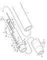
図1は、この発明による静電容量方式の電子ペンの第1の実施形態の構成例を説明するための図であり、図1(A)は、この実施形態の静電容量方式の電子ペン1の外観を示す図、図1(B)は、そのペン先側の縦断面図である。また、図2は、この第1の実施形態の静電容量方式の電子ペン1のペン筐体10の構成を説明するための分解斜視図である。
FIG. 1 is a diagram for explaining a configuration example of the first embodiment of the capacitance type electronic pen according to the present invention, and FIG. 1 (A) is a diagram for explaining a configuration example of the capacitance type electronic pen of this embodiment. FIG. 1 (B), which shows the appearance of FIG. 1, is a vertical cross-sectional view of the pen tip side. Further, FIG. 2 is an exploded perspective view for explaining the configuration of the pen housing 10 of the capacitance type electronic pen 1 of the first embodiment.
この第1の実施形態の電子ペン1においては、ペン筐体10は、図1(A),(B)に示すように、導電部材、例えば導電性金属からなる筐体筒状部11のペン先側に、絶縁部材、例えば樹脂からなる筒状結合部材13を介して、導電部材、例えば導電性金属からなる周辺電極12が結合され、この周辺電極12のペン先側にフロントキャップ14が結合されて構成されている。筒状結合部材13は、筐体筒状部11と周辺電極12との間の絶縁の役割をする。
In the electronic pen 1 of the first embodiment, as shown in FIGS. 1A and 1B, the pen housing 10 is a pen of a housing tubular portion 11 made of a conductive member, for example, a conductive metal. A conductive member, for example, a peripheral electrode 12 made of a conductive metal is bonded to the front side via an insulating member, for example, a tubular coupling member 13 made of resin, and a front cap 14 is bonded to the pen tip side of the peripheral electrode 12. It is composed of. The tubular coupling member 13 serves as an insulator between the housing tubular portion 11 and the peripheral electrodes 12.
周辺電極12は、この例では、図1(A),(B)及び図2に示すように、外径が一定の径の円筒形状部12aと、ペン先側に向かって徐々に先細となるようにテーパー状に形成されているテーパー部12bとを有する形状とされている。筐体筒状部11は、この例では、図1(A),(B)及び図2に示すように、周辺電極12の円筒形状部12aの外径と等しい外径の円筒形状を有している。フロントキャップ14は、周辺電極12のテーパー部12bの先細の先端に取り付けられている。
In this example, the peripheral electrode 12 gradually tapers toward the pen tip side and the cylindrical portion 12a having a constant outer diameter, as shown in FIGS. 1 (A), 1 (B) and 2. It has a shape having a tapered portion 12b formed in a tapered shape as described above. In this example, the housing tubular portion 11 has a cylindrical shape having an outer diameter equal to the outer diameter of the cylindrical portion 12a of the peripheral electrode 12, as shown in FIGS. 1 (A), 1 (B) and 2. ing. The front cap 14 is attached to the tapered tip of the tapered portion 12b of the peripheral electrode 12.
筒状結合部材13は、図1(B)及び図2に示すような筒状体であって、軸心方向の中ほどの位置には、外周面から突出するリング状鍔部13Fが形成されている。このリング状鍔部13Fは、軸心方向に所定の幅W(図1(A)、(B)及び図2参照)を有し、その端面は、図1(A)及び(B)に示すように、筐体筒状部11及び周辺電極12と段差を生じることなく面一となってペン筐体10の一部を構成するようにされている。
The tubular connecting member 13 is a tubular body as shown in FIGS. 1B and 2, and a ring-shaped flange portion 13F protruding from the outer peripheral surface is formed at a position in the middle in the axial direction. ing. The ring-shaped flange portion 13F has a predetermined width W (see FIGS. 1 (A), (B) and 2) in the axial direction, and its end faces are shown in FIGS. 1 (A) and 1 (B). As described above, the pen housing 10 is formed so as to be flush with the housing tubular portion 11 and the peripheral electrodes 12 without forming a step.
そして、この筒状結合部材13の、リング状鍔部13Fよりも軸心方向の一方側であるペン先側は、周辺電極12の円筒形状部12aと嵌合される第1の嵌合筒状部13aとされる。また、筒状結合部材13のリング状鍔部13Fよりも軸心方向に後端側は、筐体筒状部11と嵌合される第2の嵌合筒状部13bとされる。
The pen tip side of the tubular coupling member 13, which is one side in the axial direction from the ring-shaped flange portion 13F, has a first fitting tubular shape that is fitted with the cylindrical portion 12a of the peripheral electrode 12. It is referred to as a part 13a. Further, the rear end side of the tubular coupling member 13 in the axial direction with respect to the ring-shaped flange portion 13F is a second fitting tubular portion 13b that is fitted with the housing tubular portion 11.
筐体筒状部11と周辺電極12とが筒状結合部材13に対して図2で矢印で示すように挿入されて嵌合され、さらに周辺電極12のペン先側の開口12c(図2参照)にフロントキャップ14が結合された状態では、図1(A)に示すように、1本の筒状体のペン筐体10が形成される。このとき、前述したように、筐体筒状部11の外周面と、周辺電極12の外周面と、筒状結合部材13のリング状鍔部13Fの端面とは面一の状態となっている。そして、導電性材料からなる筐体筒状部11と周辺電極12とは、筒状結合部材13のリング状鍔部13Fの存在により接触することなく互いに電気的に分離(絶縁)されている状態となっている。
The housing tubular portion 11 and the peripheral electrode 12 are inserted and fitted into the tubular coupling member 13 as shown by an arrow in FIG. 2, and further, the opening 12c on the pen tip side of the peripheral electrode 12 (see FIG. 2). ) Is connected to the front cap 14, and as shown in FIG. 1 (A), one tubular pen housing 10 is formed. At this time, as described above, the outer peripheral surface of the housing tubular portion 11, the outer peripheral surface of the peripheral electrode 12, and the end surface of the ring-shaped flange portion 13F of the tubular coupling member 13 are flush with each other. .. The housing tubular portion 11 and the peripheral electrode 12 made of a conductive material are electrically separated (insulated) from each other without contacting each other due to the presence of the ring-shaped flange portion 13F of the tubular coupling member 13. It has become.
ペン筐体10の内部には、図1(B)に示すように、中空部10aが存在する。周辺電極12のペン先側に装着されるフロントキャップ14は絶縁材からなり、その先端側に、中心電極を構成する芯体15の径よりも大きな径の開口14a(図1(B)参照)を備えており、その開口14aは、ペン筐体10の中空部10aに連通している。
As shown in FIG. 1 (B), a hollow portion 10a exists inside the pen housing 10. The front cap 14 mounted on the pen tip side of the peripheral electrode 12 is made of an insulating material, and an opening 14a having a diameter larger than the diameter of the core body 15 constituting the center electrode is formed on the tip side thereof (see FIG. 1 (B)). The opening 14a communicates with the hollow portion 10a of the pen housing 10.
そして、芯体15が、図1(B)に示すように、フロントキャップ14の開口14aから、ペン筐体10の中空部10a内に挿入される。芯体15は、導電性材料、例えば導電性金属で構成され、図1(B)に示すような棒状体からなる。芯体15は、その先端部15aが外部に突出する状態で、ペン筐体10内に設けられる後述する芯体保持部材2に着脱可能に嵌合されて保持されるように構成されている。また、ペン筐体10の筐体筒状部11のペン先側とは反対側の後端側の開口は、この例では、図1(A)に示すように、例えば樹脂からなる蓋部16により閉塞されている。
Then, as shown in FIG. 1 (B), the core body 15 is inserted into the hollow portion 10a of the pen housing 10 through the opening 14a of the front cap 14. The core body 15 is made of a conductive material, for example, a conductive metal, and is made of a rod-shaped body as shown in FIG. 1 (B). The core body 15 is configured to be detachably fitted and held in a core body holding member 2 provided in the pen housing 10 in a state where the tip portion 15a protrudes to the outside. Further, in this example, as shown in FIG. 1A, the opening on the rear end side of the housing tubular portion 11 of the pen housing 10 opposite to the pen tip side is a lid portion 16 made of, for example, resin. Is blocked by.
導電性材料からなる芯体15と周辺電極12とは、図1(B)に示すように、絶縁材であるフロントキャップ14により、電気的に分離(絶縁)される。この第1の実施形態の電子ペン1においては、芯体15が装着されたときには、図1(B)に示すように、芯体15のペン先となる先端部15aよりも後端側が周辺電極12に囲まれるような状態となるように構成されている。
As shown in FIG. 1 (B), the core body 15 made of a conductive material and the peripheral electrode 12 are electrically separated (insulated) by the front cap 14 which is an insulating material. In the electronic pen 1 of the first embodiment, when the core body 15 is attached, as shown in FIG. 1B, the peripheral electrode is on the rear end side of the tip portion 15a which is the pen tip of the core body 15. It is configured to be surrounded by twelve.
ペン筐体10の中空部10a内には、図1(B)において点線で示すように、芯体保持部材2、筆圧検出部3、信号発信回路を含む電子回路が搭載されるプリント基板4、電子回路への電源電圧供給用の蓄電デバイスの例としてのコンデンサ5が、ペン先側から順に、軸心方向に並べられて収納されて、配設されている。プリント基板4に搭載される電子回路には、コンデンサ5への充電電流を供給するための充電用回路が含まれている。この実施形態では、後述するように、電界結合による非接触の電力伝送方式で外部から伝送される電力を受けてコンデンサ5は充電される。この例では、コンデンサ5は、例えば電気二重層コンデンサで構成される。
As shown by the dotted line in FIG. 1B, the hollow portion 10a of the pen housing 10 is a printed circuit board 4 on which an electronic circuit including a core body holding member 2, a pen pressure detection unit 3, and a signal transmission circuit is mounted. , Capacitors 5 as an example of a power storage device for supplying a power supply voltage to an electronic circuit are arranged and arranged in order from the pen tip side in the axial direction. The electronic circuit mounted on the printed circuit board 4 includes a charging circuit for supplying a charging current to the capacitor 5. In this embodiment, as will be described later, the capacitor 5 is charged by receiving electric power transmitted from the outside by a non-contact electric power transmission method by electric field coupling. In this example, the capacitor 5 is composed of, for example, an electric double layer capacitor.
そして、この第1の実施形態では、ペン筐体10の中空部10a内には、図1(B)に示すように、基板載置台部61にプリント基板4が載置される基板ホルダー6が収納されている。
Then, in the first embodiment, as shown in FIG. 1B, a substrate holder 6 on which the printed circuit board 4 is mounted on the substrate mounting base 61 is provided in the hollow portion 10a of the pen housing 10. It is stored.
基板ホルダー6は、絶縁性の樹脂により構成され、電子ペン1の軸心方向となる長手方向において、基板載置台部61側とは反対側に、筆圧検出部3を収納保持するための筆圧検出部保持部62を有している。筆圧検出部保持部62は、内部の中空部に筆圧検出部3の複数個の部品を収納する中空部を備える円筒形状とされる。基板載置台部61は、プリント基板4を載置して保持するボート状の形状であって、筒状体を軸芯方向に略半分切断したような形状とされている。
The substrate holder 6 is made of an insulating resin, and is a brush for accommodating and holding the pen pressure detecting portion 3 on the side opposite to the substrate mounting base portion 61 side in the longitudinal direction which is the axial direction of the electronic pen 1. It has a pressure detection unit holding unit 62. The pen pressure detection unit holding unit 62 has a cylindrical shape having a hollow portion inside which contains a plurality of parts of the pen pressure detection unit 3. The substrate mounting base 61 has a boat-like shape on which the printed circuit board 4 is placed and held, and is shaped like a tubular body cut in substantially half in the axial direction.
基板ホルダー6は、図1(B)に示すように、筆圧検出部保持部62がペン先側となるように、ペン筐体10内に収納される。そして、この筆圧検出部保持部62に保持されている筆圧検出部3に対して、芯体15と嵌合して当該芯体15を保持する芯体保持部材2が結合され、芯体15に印加される圧力(筆圧)が、筆圧検出部3に伝達されるように構成されている。
As shown in FIG. 1 (B), the substrate holder 6 is housed in the pen housing 10 so that the pen pressure detection unit holding portion 62 is on the pen tip side. Then, the core body holding member 2 that fits with the core body 15 and holds the core body 15 is coupled to the pen pressure detection unit 3 held by the pen pressure detection unit holding unit 62, and the core body is formed. The pressure (pen pressure) applied to the pen 15 is configured to be transmitted to the pen pressure detecting unit 3.
基板ホルダー6の筆圧検出部保持部62の外径は、この実施形態では、筒状結合部材13の内径と等しいあるいは若干小さく選定されている。そして、図2に示すように、基板ホルダー6の筆圧検出部保持部62の一部が、筒状結合部材13の嵌合筒状部13bの一部と嵌合することで、基板ホルダー6が、ペン筐体10内において軸心方向に移動しないように位置規制されている。
In this embodiment, the outer diameter of the pen pressure detection unit holding portion 62 of the substrate holder 6 is selected to be equal to or slightly smaller than the inner diameter of the tubular coupling member 13. Then, as shown in FIG. 2, a part of the pen pressure detecting portion holding portion 62 of the substrate holder 6 is fitted with a part of the fitting tubular portion 13b of the tubular coupling member 13, so that the substrate holder 6 is fitted. However, the position is restricted so as not to move in the axial direction in the pen housing 10.
芯体15を嵌合保持する芯体保持部材2は、図1(B)及び図3に示すように、導電性弾性部材21と、芯体ホルダー22と、コイルばね23と、導体端子部材24とから構成されている。芯体15は、この実施形態では、図1(B)に示すように、導電性弾性部材21を介して導電性材料からなる芯体ホルダー22に嵌合されることにより、芯体ホルダー22に対して結合保持されている。芯体保持部材2は、筆圧検出部3に対して、芯体15に印可される筆圧の伝達部材の役割もする。
As shown in FIGS. 1B and 3, the core body holding member 2 for fitting and holding the core body 15 includes a conductive elastic member 21, a core body holder 22, a coil spring 23, and a conductor terminal member 24. It is composed of and. In this embodiment, the core body 15 is fitted into the core body holder 22 made of a conductive material via the conductive elastic member 21 as shown in FIG. 1 (B). On the other hand, the bond is held. The core body holding member 2 also serves as a pen pressure transmitting member applied to the core body 15 with respect to the pen pressure detecting unit 3.
そして、芯体ホルダー22が、筆圧検出部保持部62に保持される筆圧検出部3の保持部材33に嵌合されることにより、芯体15に印加される圧力(筆圧)が筆圧検出部3に伝達されるように構成されている。この場合に、芯体ホルダー22は、導電性金属などの導電性材料からなる弾性部材の例としてのコイルばね23により、基板ホルダー6に対して常に芯体15側に付勢されるように構成されている。なお、コイルばね23は、導体端子部材24と共に、プリント基板4に配設されている電子回路の信号発信回路からの信号を芯体15に伝達するための電気的接続用部材を構成するものである。
Then, the core body holder 22 is fitted to the holding member 33 of the writing pressure detecting unit 3 held by the writing pressure detecting unit holding unit 62, so that the pressure (pen pressure) applied to the core body 15 is applied to the writing brush. It is configured to be transmitted to the pressure detection unit 3. In this case, the core holder 22 is configured to be always urged toward the core 15 with respect to the substrate holder 6 by a coil spring 23 as an example of an elastic member made of a conductive material such as a conductive metal. Has been done. The coil spring 23, together with the conductor terminal member 24, constitutes an electrical connection member for transmitting a signal from the signal transmission circuit of the electronic circuit arranged on the printed circuit board 4 to the core body 15. be.
図3(A)は、芯体15、導電性弾性部材21、芯体ホルダー22、コイルばね23、導体端子部材24及び基板ホルダー6の筆圧検出部保持部62の部分の分解斜視図である。
FIG. 3A is an exploded perspective view of a core body 15, a conductive elastic member 21, a core body holder 22, a coil spring 23, a conductor terminal member 24, and a pressure detecting portion holding portion 62 of the substrate holder 6. ..
導電性弾性部材21は、例えば導電性ゴムからなり、芯体15の先端部15aとは反対側の端部が嵌合される貫通孔21aを備える円筒状形状に形成されている。この導電性弾性部材21の芯体15側は、他の部分よりも外径が小さくされて薄肉部とされると共に、スリット212が形成されて、芯体15を把持し易くする把持部211とされている。
The conductive elastic member 21 is made of, for example, conductive rubber, and is formed in a cylindrical shape having a through hole 21a into which an end portion of the core body 15 opposite to the tip portion 15a is fitted. The core body 15 side of the conductive elastic member 21 has an outer diameter smaller than that of other parts to form a thin-walled portion, and a slit 212 is formed to facilitate gripping the core body 15. Has been done.
このように構成したことにより、芯体15は、把持部211の、スリット212が形成された2個の薄肉部である弧状部分により把持される。したがって、芯体15は導電性弾性部材21の把持部211に対して容易に挿入嵌合され、また、所定の力で引っ張ることで、芯体15を導電性弾性部材21から容易に引き抜くことができる。
With this configuration, the core body 15 is gripped by the arc-shaped portion of the grip portion 211, which is two thin-walled portions having slits 212 formed therein. Therefore, the core body 15 can be easily inserted and fitted to the grip portion 211 of the conductive elastic member 21, and the core body 15 can be easily pulled out from the conductive elastic member 21 by pulling with a predetermined force. can.
芯体ホルダー22は、導電性材料、例えばSUS(Steel Special Use Stainless)からなり、導電性弾性部材21を収納嵌合する凹穴221aを有する収納嵌合部221と、筆圧検出部3の後述する保持部材33に嵌合する棒状部222とが一体に形成されたものである。
The core holder 22 is made of a conductive material, for example, SUS (Steel Special Use Stainless), and has a storage fitting portion 221 having a concave hole 221a for accommodating and fitting the conductive elastic member 21, and a pen pressure detecting portion 3 described later. The rod-shaped portion 222 that fits into the holding member 33 is integrally formed.
上述のようにして導電性弾性部材21を収納した芯体ホルダー22の棒状部222に導電性のコイルばね23が装着された後、芯体ホルダー22の棒状部222は、基板ホルダー6の筆圧検出部保持部62に保持される筆圧検出部3の保持部材33に嵌合される。
After the conductive coil spring 23 is attached to the rod-shaped portion 222 of the core body holder 22 accommodating the conductive elastic member 21 as described above, the rod-shaped portion 222 of the core body holder 22 is subjected to the writing pressure of the substrate holder 6. It is fitted to the holding member 33 of the pen pressure detection unit 3 held by the detection unit holding unit 62.
この場合に、この実施形態の電子ペン1においては、プリント基板4上に構成されている電子回路の信号発信回路からの送信信号を、芯体15に供給する必要がある。この実施形態では、芯体ホルダー22と、基板ホルダー6の筆圧検出部保持部62との間に設けた、導電性の材料で構成されたコイルばね23と、基板ホルダー6の筆圧検出部保持部62に設けられた導体端子部材24(図3(B)参照)とにより電気的接続用部材を構成し、この電気的接続用部材により、プリント基板4の信号発信回路からの信号供給のための電気的接続を実現している。
In this case, in the electronic pen 1 of this embodiment, it is necessary to supply the transmission signal from the signal transmission circuit of the electronic circuit configured on the printed circuit board 4 to the core body 15. In this embodiment, a coil spring 23 made of a conductive material and a pressure detecting portion of the substrate holder 6 are provided between the core holder 22 and the pressure detecting portion holding portion 62 of the substrate holder 6. A conductor terminal member 24 (see FIG. 3B) provided in the holding portion 62 constitutes an electrical connection member, and the electrical connection member supplies a signal from the signal transmission circuit of the printed circuit board 4. Realizes an electrical connection for.
導体端子部材24は、導電性を有する材料、例えばSUSからなり、図3(A),(B)に示すように、基板ホルダー6の筆圧検出部保持部62の開口部62a側を覆い、かつ、芯体ホルダー22の棒状部222が挿通する貫通孔241aを備える当接板部241を有する。また、導体端子部材24は、基板ホルダー6の筆圧検出部保持部62の部分を跨いで、基板載置台部61の部分まで延伸する延伸部242備えている。そして、導体端子部材24が基板ホルダー6の筆圧検出部保持部62に装着された状態においては、図1(B)に示すように、導体端子部材24から延伸する延伸部242の先端の端子部242aは、基板ホルダー6の基板載置台部61に載置されているプリント基板4の裏面側の導体と当接し、例えば半田付けされる。これにより、導体端子部材24とプリント基板4に設けられている信号発信回路と電気的に接続される。
The conductor terminal member 24 is made of a conductive material, for example, SUS, and as shown in FIGS. 3A and 3B, covers the opening 62a side of the pressure detecting portion holding portion 62 of the substrate holder 6. Moreover, it has a contact plate portion 241 provided with a through hole 241a through which the rod-shaped portion 222 of the core body holder 22 is inserted. Further, the conductor terminal member 24 is provided with an extension portion 242 that straddles the portion of the pen pressure detection portion holding portion 62 of the substrate holder 6 and extends to the portion of the substrate mounting base portion 61. Then, in a state where the conductor terminal member 24 is mounted on the pen pressure detecting portion holding portion 62 of the substrate holder 6, as shown in FIG. 1 (B), the terminal at the tip of the extending portion 242 extending from the conductor terminal member 24. The portion 242a comes into contact with the conductor on the back surface side of the printed circuit board 4 mounted on the substrate mounting base portion 61 of the substrate holder 6, and is soldered, for example. As a result, the conductor terminal member 24 is electrically connected to the signal transmission circuit provided on the printed circuit board 4.
そして、コイルばね23は、芯体ホルダー22に弾性的に接触すると共に、導体端子部材24の当接板部241に当接して弾性的に接触する。コイルばね23は、導電性材料で構成されていると共に、導電性弾性部材21及び芯体ホルダー22は導電性を有するので、コイルばね23及び導体端子部材24を介して、芯体ホルダー22に嵌合されている導電性弾性部材21は、プリント基板4の回路部と電気的に接続される。
Then, the coil spring 23 elastically contacts the core holder 22, and also elastically contacts the contact plate portion 241 of the conductor terminal member 24. Since the coil spring 23 is made of a conductive material and the conductive elastic member 21 and the core holder 22 are conductive, the coil spring 23 is fitted into the core holder 22 via the coil spring 23 and the conductor terminal member 24. The combined conductive elastic member 21 is electrically connected to the circuit portion of the printed circuit board 4.
以上のようにペン筐体10内に収納された芯体ホルダー22に嵌合された導電性弾性部材21の貫通孔21aに対して、芯体15が、前述したようにして挿入嵌合されて、芯体15が、芯体ホルダー22に対して、導電性弾性部材21を介して保持される。この状態では、芯体15は、プリント基板4の信号発信回路と電気的に接続されることになり、信号発信回路からの信号が芯体15に供給される状態となる。
As described above, the core body 15 is inserted and fitted into the through hole 21a of the conductive elastic member 21 fitted in the core body holder 22 housed in the pen housing 10 as described above. , The core body 15 is held by the core body holder 22 via the conductive elastic member 21. In this state, the core body 15 is electrically connected to the signal transmission circuit of the printed circuit board 4, and the signal from the signal transmission circuit is supplied to the core body 15.
この例の筆圧検出部3は、図1(B)に示すように、誘電体31と、端子部材32と、保持部材33と、導電部材34と、弾性部材35との複数個の部品からなる周知の構成を備え、芯体15に印加される筆圧に応じて静電容量が変化する容量可変コンデンサの構成である。
As shown in FIG. 1 (B), the pen pressure detecting unit 3 of this example is composed of a plurality of parts including a dielectric 31, a terminal member 32, a holding member 33, a conductive member 34, and an elastic member 35. This is a configuration of a variable capacitance capacitor having a well-known configuration, the capacitance of which changes according to the writing pressure applied to the core body 15.
次に、周辺電極12と、プリント基板4の回路部との電気的な接続について説明する。
Next, the electrical connection between the peripheral electrode 12 and the circuit portion of the printed circuit board 4 will be described.
ここで、図2は、基板ホルダー6を基板載置台部61とは反対側から見たときの筐体筒状部11及び周辺電極12、さらに、筒状結合部材13を示している。この図2に示すように、筒状結合部材13の外周面には、凹溝13cが、当該筒状結合部材13の軸心方向に沿った方向に、第1の嵌合筒状部13aから、リング状鍔部13Fの下部を通って、第2の嵌合筒状部13bに亘って形成されている。そして、基板ホルダー6の筆圧検出部保持部62の周側面には、第2の嵌合筒状部13bの凹溝13cと連続するような凹溝62aが形成されている。また、基板ホルダー6の基板載置台部61には、図2に示すように、切欠き部61aが形成されて、載置されるプリント基板4の裏面4b側が、この切欠き部61a側から見えるような状態に構成されている。
Here, FIG. 2 shows the housing tubular portion 11, the peripheral electrodes 12, and the tubular coupling member 13 when the substrate holder 6 is viewed from the side opposite to the substrate mounting base portion 61. As shown in FIG. 2, a concave groove 13c is formed on the outer peripheral surface of the tubular coupling member 13 from the first fitting tubular portion 13a in the direction along the axial direction of the tubular coupling member 13. , It is formed over the second fitting tubular portion 13b through the lower part of the ring-shaped flange portion 13F. A concave groove 62a is formed on the peripheral side surface of the pen pressure detecting portion holding portion 62 of the substrate holder 6 so as to be continuous with the concave groove 13c of the second fitting tubular portion 13b. Further, as shown in FIG. 2, a notch portion 61a is formed in the substrate mounting base portion 61 of the substrate holder 6, and the back surface 4b side of the printed circuit board 4 on which the printed circuit board 4 is placed can be seen from the notch portion 61a side. It is configured in such a state.
そして、図2に示すように、凹溝13c及び凹溝62a内には、導電体材料、この例では、導電体金属からなる接続端子導体17が配設される。この場合に、凹溝13c及び凹溝62aの深さは、接続端子導体17の上面が、第2の嵌合筒状部13bの外周面よりも低い位置となるように構成されている。これにより、筐体筒状部11が、筒状結合部材13の第2の嵌合筒状部13bに嵌合されたときには、凹溝13c及び凹溝62a内に収納された接続端子導体17の上面と筐体筒状部11の内壁面との間には、空気層が存在して、両者が電気的分離(絶縁)される。
Then, as shown in FIG. 2, a conductor material, in this example, a connection terminal conductor 17 made of a conductor metal is disposed in the concave groove 13c and the concave groove 62a. In this case, the depths of the concave groove 13c and the concave groove 62a are configured so that the upper surface of the connection terminal conductor 17 is lower than the outer peripheral surface of the second fitting tubular portion 13b. As a result, when the housing tubular portion 11 is fitted into the second fitting tubular portion 13b of the tubular coupling member 13, the connection terminal conductor 17 housed in the concave groove 13c and the concave groove 62a An air layer exists between the upper surface and the inner wall surface of the housing tubular portion 11, and the two are electrically separated (insulated).
なお、図1(B)にも示すように、筒状結合部材13の第1の嵌合筒状部13a側の凹溝13cに配設される接続端子導体17の端部17aは、少なくとも一部が、第1の嵌合筒状部13aの外周面よりも若干膨出するように配設される。これにより、筒状結合部材13の第1の嵌合筒状部13aに周辺電極12が嵌合されたときに、接続端子導体17の端部17aと、周辺電極12の内壁とが確実に接触して、周辺電極12と接続端子導体17とが電気的に接続される状態となるように構成されている。
As shown in FIG. 1B, at least one end portion 17a of the connection terminal conductor 17 arranged in the concave groove 13c on the first fitting tubular portion 13a side of the tubular coupling member 13 is provided. The portion is arranged so as to slightly bulge from the outer peripheral surface of the first fitting tubular portion 13a. As a result, when the peripheral electrode 12 is fitted to the first fitting tubular portion 13a of the tubular coupling member 13, the end portion 17a of the connection terminal conductor 17 and the inner wall of the peripheral electrode 12 are reliably contacted. Then, the peripheral electrode 12 and the connection terminal conductor 17 are electrically connected to each other.
そして、接続端子導体17のプリント基板4側に伸びている端部17bは、基板ホルダー6の切欠き部61aのところで折り曲げられて、プリント基板4の裏面4b側に電気的に接続される。図示は省略してあるが、接続端子導体17の端部17bは、プリント基板4の表面側の回路部とはスルーホールを介して、電気的に接続されている。
Then, the end portion 17b of the connection terminal conductor 17 extending toward the printed circuit board 4 side is bent at the notch portion 61a of the substrate holder 6 and electrically connected to the back surface 4b side of the printed circuit board 4. Although not shown, the end portion 17b of the connection terminal conductor 17 is electrically connected to the circuit portion on the front surface side of the printed circuit board 4 via a through hole.
なお、接続端子導体17の上面を絶縁層で覆うようにして、より確実に接続端子導体17と筐体筒状部11との絶縁を実現するようにしてもよい。
The upper surface of the connection terminal conductor 17 may be covered with an insulating layer to more reliably insulate the connection terminal conductor 17 from the housing tubular portion 11.
そして、図1では図示を省略したが、プリント基板4に形成されている電子回路には、導電性金属からなる筐体筒状部11も電気的に接続されている。
Although not shown in FIG. 1, a housing tubular portion 11 made of a conductive metal is also electrically connected to the electronic circuit formed on the printed circuit board 4.
以上のような構成の電子ペン1は、芯体15の先端部のみではなく、この芯体15の周囲を囲むように構成されている周辺電極12が位置検出センサと静電容量を介して電界結合する。そして、位置検出センサを備える位置検出装置において、位置検出センサの検出領域内での電子ペン1による指示位置と、電子ペンの傾きの検出が可能となる。
In the electronic pen 1 having the above configuration, not only the tip portion of the core body 15 but also the peripheral electrodes 12 configured to surround the core body 15 are subjected to an electric field via a position detection sensor and a capacitance. Join. Then, in the position detection device provided with the position detection sensor, it is possible to detect the position indicated by the electronic pen 1 in the detection area of the position detection sensor and the inclination of the electronic pen.
[第1の実施形態の電子ペンの蓄電デバイスの例としてのコンデンサ5の充電]
第1の実施形態の電子ペン1においては、電界結合によるワイヤレス電力伝送技術を用いた充電方法により、ペン筐体10内に収納されている蓄電デバイスの例としてのコンデンサ5を充電するように構成されている。 [Charging thecapacitor 5 as an example of the power storage device of the electronic pen of the first embodiment]
Theelectronic pen 1 of the first embodiment is configured to charge a capacitor 5 as an example of a power storage device housed in the pen housing 10 by a charging method using a wireless power transmission technique by electric field coupling. Has been done.
第1の実施形態の電子ペン1においては、電界結合によるワイヤレス電力伝送技術を用いた充電方法により、ペン筐体10内に収納されている蓄電デバイスの例としてのコンデンサ5を充電するように構成されている。 [Charging the
The
すなわち、上述したように、第1の実施形態の電子ペン1においては、ペン筐体10は導電性の筐体筒状部11と、導電性の周辺電極12とを備えている。そこで、第1の実施形態の電子ペン1においては、コンデンサ5の充電時には、筐体筒状部11と周辺電極12とを、電界結合により電力を受ける受電電極として用い、この受電電極で受信した電力に基づいて、プリント基板4に形成されている電子回路に構成された充電回路を用いて、コンデンサ5を充電するようように構成する。
That is, as described above, in the electronic pen 1 of the first embodiment, the pen housing 10 includes a conductive housing tubular portion 11 and a conductive peripheral electrode 12. Therefore, in the electronic pen 1 of the first embodiment, when charging the capacitor 5, the housing tubular portion 11 and the peripheral electrode 12 are used as a power receiving electrode that receives power by electric field coupling, and the capacitor 5 receives the power. Based on the electric power, the charging circuit configured in the electronic circuit formed on the printed circuit board 4 is used to charge the capacitor 5.
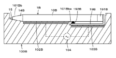
この実施形態では、充電装置として、電子ペン1を載置することでワイヤレス充電が可能となる電子ペン用の充電トレーを用いる。図4は、この電子ペン用の充電トレーの一例を、電子ペン1と共に示す図である。図4(A)は、この例の電子ペン用の充電トレー100を斜め上方から見た斜視図、図4(B)は、この例の電子ペン用の充電トレー100の側面図であり、当該電子ペン用の充電トレー100に、電子ペン1を載置した状態を説明するための図である。
In this embodiment, as the charging device, a charging tray for an electronic pen that enables wireless charging by mounting the electronic pen 1 is used. FIG. 4 is a diagram showing an example of a charging tray for the electronic pen together with the electronic pen 1. FIG. 4A is a perspective view of the charging tray 100 for the electronic pen of this example viewed from diagonally above, and FIG. 4B is a side view of the charging tray 100 for the electronic pen of this example. It is a figure for demonstrating the state which put the electronic pen 1 on the charging tray 100 for an electronic pen.
すなわち、図4の例の電子ペン用の充電トレー100は、電子ペン1のペン筐体10の太さよりも厚さの厚い、この例では、直方体形状のトレー筐体101を備える構成とされている。このトレー筐体101は、絶縁部材、この例では樹脂で構成され、その上面101aの長辺方向の長さは、この例では、電子ペン1の軸心方向の長さよりも長いものとされていると共に、短辺方向の長さは、電子ペン1の太さよりも大きい長さとされている。
That is, the charging tray 100 for the electronic pen in the example of FIG. 4 is configured to include a rectangular parallelepiped tray housing 101 that is thicker than the pen housing 10 of the electronic pen 1. There is. The tray housing 101 is made of an insulating member, in this example, a resin, and the length of the upper surface 101a in the long side direction is longer than the length in the axial direction of the electronic pen 1 in this example. At the same time, the length in the short side direction is set to be larger than the thickness of the electronic pen 1.
そして、この例では、図4(A)に示すように、トレー筐体101の上面101aの短辺方向の中央部には、長辺方向に沿って、電子ペン1の軸心方向の長さよりも若干長い窪み101bが設けられている。この窪み101bは、電子ペン1の収容及び載置用であり、この窪み101bの幅は、電子ペン1の太さよりも大きく構成されている。ただし、この窪み101bは、電子ペン1のペン筐体10のペン先側の形状に合わせた形状とされており、電子ペン1のペン筐体10のペン先が収容される長手方向の一端側の幅は、徐々に幅が狭くなるように形成されている。
Then, in this example, as shown in FIG. 4A, the central portion of the upper surface 101a of the tray housing 101 in the short side direction is located along the long side direction from the length in the axial direction of the electronic pen 1. Also provided with a slightly longer recess 101b. The recess 101b is for accommodating and placing the electronic pen 1, and the width of the recess 101b is larger than the thickness of the electronic pen 1. However, the recess 101b has a shape that matches the shape of the pen housing 10 of the electronic pen 1 on the pen tip side, and is one end side in the longitudinal direction in which the pen tip of the pen housing 10 of the electronic pen 1 is housed. The width of is formed so that the width gradually narrows.
使用者は、電子ペン1のコンデンサ5の充電をしようとするときには、この電子ペン用充電トレー100の窪み101bの形状に合わせて、電子ペン1を、図4(A)に示すように、周辺電極12が設けられているペン先側が、窪み101bの、徐々に幅が狭くなる一端側となるような状態で、この窪み101b内に収納するように載置するようにする。
When the user intends to charge the capacitor 5 of the electronic pen 1, the electronic pen 1 is moved to the periphery as shown in FIG. 4 (A) according to the shape of the recess 101b of the charging tray 100 for the electronic pen. The pen tip side on which the electrode 12 is provided is placed so as to be housed in the recess 101b in a state where the pen tip side is one end side of the recess 101b whose width gradually narrows.
電子ペン用充電トレー100のトレー筐体101の内部には、窪み部101bの長手方向に沿って、送電電極102及び103が配設されている。この場合に、送電電極102及び103は、窪み101bの底面から露出することなく、当該底面と送電電極102及び103の電極表面との間に、例えばトレー筐体101を構成する樹脂からなる層1010s(図4(B)参照)が介在するように構成されている。そして、電子ペン1を窪み101b内に収容するように載置したときに、送電電極102と電子ペン1の筐体筒状部11とが樹脂の層101sを介して対向すると共に、送電電極103と電子ペン1の周辺電極12とが樹脂の層101sを介して対向するように、送電電極102及び103が配設されている。
Inside the tray housing 101 of the charging tray 100 for an electronic pen, power transmission electrodes 102 and 103 are arranged along the longitudinal direction of the recessed portion 101b. In this case, the power transmission electrodes 102 and 103 are not exposed from the bottom surface of the recess 101b, and between the bottom surface and the electrode surfaces of the power transmission electrodes 102 and 103, for example, a layer 1010s made of resin constituting the tray housing 101. (See FIG. 4 (B)) is configured to intervene. Then, when the electronic pen 1 is placed so as to be accommodated in the recess 101b, the power transmission electrode 102 and the housing tubular portion 11 of the electronic pen 1 face each other via the resin layer 101s, and the power transmission electrode 103 The power transmission electrodes 102 and 103 are arranged so that the peripheral electrodes 12 of the electronic pen 1 and the peripheral electrodes 12 of the electronic pen 1 face each other with the resin layer 101s.
送電電極102及び103の電極表面と窪み101bの底面との間の層101sの厚さは、当該送電電極102及び103と、電子ペン1の受電電極を構成する周辺電極12及び筐体筒状部11との結合容量Cmによる電界結合の強さが適切になるように選定されており、例えば1~数ミリメートルとされている。
The thickness of the layer 101s between the electrode surfaces of the power transmission electrodes 102 and 103 and the bottom surface of the recess 101b is the thickness of the power transmission electrodes 102 and 103, the peripheral electrodes 12 constituting the power receiving electrodes of the electronic pen 1, and the housing tubular portion. The strength of the electric field coupling due to the coupling capacitance Cm with 11 is selected to be appropriate, and is set to, for example, 1 to several millimeters.
そして、充電トレー100のトレー筐体101には、送電電極102及び103から送電電力を送出するために、送電電極102及び103に供給する交流電流を供給する交流信号発生回路104が設けられている。
The tray housing 101 of the charging tray 100 is provided with an AC signal generation circuit 104 that supplies an AC current to be supplied to the power transmission electrodes 102 and 103 in order to transmit power to be transmitted from the power transmission electrodes 102 and 103. ..
なお、窪み101bの深さは、この窪み101bに電子ペン1が置かれたときに、電子ペン1の筐体筒状部11及び周辺電極12と、送電電極102及び103との電界結合が適切な強さとなるような深さとされている。
The depth of the recess 101b is such that when the electronic pen 1 is placed in the recess 101b, the electric field coupling between the housing tubular portion 11 and the peripheral electrodes 12 of the electronic pen 1 and the power transmission electrodes 102 and 103 is appropriate. It is said to have a depth that makes it strong.
なお、図4では、図示を省略するが、この電子ペン用充電トレー100は、商用交流電源のコンセントに嵌合されるACプラグが接続されていると共に、電源スイッチを備えている。
Although not shown in FIG. 4, the charging tray 100 for an electronic pen is connected to an AC plug fitted to an outlet of a commercial AC power supply and is provided with a power switch.
以上のように構成されている電子ペン用充電トレー100を用いて、電子ペン1の充電を行うには、電子ペン1を電子ペン用充電トレー100の窪み101b内に置き、電源スイッチをオンとする。すると、交流信号発生回路104に電源電圧が供給されて、交流信号発生回路104からの交流信号が送電電極102及び103に流れ、窪み101bに収容載置されている電子ペン1の筐体筒状部11及び周辺電極12と、送電電極102及び103とに電界結合により送信電力を伝達する。
To charge the electronic pen 1 using the electronic pen charging tray 100 configured as described above, place the electronic pen 1 in the recess 101b of the electronic pen charging tray 100 and turn on the power switch. do. Then, the power supply voltage is supplied to the AC signal generation circuit 104, the AC signal from the AC signal generation circuit 104 flows to the power transmission electrodes 102 and 103, and the housing tubular shape of the electronic pen 1 housed and placed in the recess 101b. Transmission power is transmitted to the unit 11 and the peripheral electrodes 12 and the power transmission electrodes 102 and 103 by electric current coupling.
電子ペン1では、筐体筒状部11及び周辺電極12で受電した電力に基づいて、電子回路の充電回路により蓄電デバイスの例としてのコンデンサ5が充電される。この充電により、電子ペン1は、アクティブ静電容量方式の電子ペンの動作が可能な状態となる。
In the electronic pen 1, the capacitor 5 as an example of the power storage device is charged by the charging circuit of the electronic circuit based on the electric power received by the housing tubular portion 11 and the peripheral electrode 12. By this charging, the electronic pen 1 is in a state where the active capacitance type electronic pen can operate.
なお、電子ペン用の充電装置としては、図4の例ようなトレーに限られるものではなく、例えば、電子ペンを挿入するペン立ての形状のようなものであってもよい。
The charging device for the electronic pen is not limited to the tray as shown in FIG. 4, but may be, for example, the shape of a pen stand into which the electronic pen is inserted.
[第1の実施形態の電子ペン1の電子回路の構成例及び電子ペン用の充電トレー100の電気的な構成例]
次に、この第1の実施形態の電子ペン1の電子回路の構成例を、電子ペン用の充電トレー100の電気的な構成例と共に図5に示す。 [Example of Configuration of Electronic Circuit ofElectronic Pen 1 of First Embodiment and Example of Electrical Configuration of Charging Tray 100 for Electronic Pen]
Next, a configuration example of the electronic circuit of theelectronic pen 1 of the first embodiment is shown in FIG. 5 together with an electrical configuration example of the charging tray 100 for the electronic pen.
次に、この第1の実施形態の電子ペン1の電子回路の構成例を、電子ペン用の充電トレー100の電気的な構成例と共に図5に示す。 [Example of Configuration of Electronic Circuit of
Next, a configuration example of the electronic circuit of the
この第1の実施形態の電子ペン1においては、電子回路は、図5に示すように、位置検出センサと信号の授受を行う電子ペン回路200と、コンデンサ5の充電回路210とからなる。
In the electronic pen 1 of the first embodiment, as shown in FIG. 5, the electronic circuit includes an electronic pen circuit 200 that sends and receives a position detection sensor and a signal, and a charging circuit 210 of the capacitor 5.
電子ペン回路200は、この例では、図5に示すように、プリント基板4に載置されているIC(Integrated Circuit)により構成される制御回路201を備える。電子ペン回路200においては、この制御回路201に対して、信号発信回路202と信号受信回路203とが接続されると共に、筆圧検出部3で構成される可変容量コンデンサ3Cが接続されている。可変容量コンデンサ3Cには、並列に抵抗3Rが接続されている。
In this example, the electronic pen circuit 200 includes a control circuit 201 composed of an IC (Integrated Circuit) mounted on the printed circuit board 4, as shown in FIG. In the electronic pen circuit 200, the signal transmitting circuit 202 and the signal receiving circuit 203 are connected to the control circuit 201, and the variable capacitance capacitor 3C composed of the pen pressure detection unit 3 is connected to the control circuit 201. A resistor 3R is connected in parallel to the variable capacitor 3C.
信号発信回路202の信号出力端は、スイッチ回路204を通じて、芯体15に接続されている。スイッチ回路204は、制御回路201からの切替制御信号SW2によりオン、オフ制御される。この場合、芯体15と、スイッチ回路204との間の電気的な接続路は、導体端子部材24及び芯体ホルダー22並びに導電性弾性部材21が介在するのは前述した通りである。
The signal output end of the signal transmission circuit 202 is connected to the core body 15 through the switch circuit 204. The switch circuit 204 is turned on and off by the switching control signal SW2 from the control circuit 201. In this case, as described above, the conductor terminal member 24, the core holder 22, and the conductive elastic member 21 are interposed in the electrical connection path between the core 15 and the switch circuit 204.
そして、この実施形態では、ペン筐体10の筐体筒状部11が、切替スイッチ回路221の可動端子Mに接続され、周辺電極12が、切替スイッチ回路222の可動端子Mに接続される。この場合、周辺電極12は、接続端子導体17を通じて切替スイッチ回路205と接続される。
Then, in this embodiment, the housing tubular portion 11 of the pen housing 10 is connected to the movable terminal M of the changeover switch circuit 221 and the peripheral electrode 12 is connected to the movable terminal M of the changeover switch circuit 222. In this case, the peripheral electrode 12 is connected to the changeover switch circuit 205 through the connection terminal conductor 17.
これら切替スイッチ回路221及び222は、固定端子CHと固定端子Pとを有し、この実施形態では、制御回路201からの後述する切替制御信号SW1により、可動端子Mを固定端子CHに接続する状態と、固定端子Pに接続する状態とに選択的に切り替えられる。
These changeover switch circuits 221 and 222 have a fixed terminal CH and a fixed terminal P, and in this embodiment, a state in which the movable terminal M is connected to the fixed terminal CH by a changeover control signal SW1 described later from the control circuit 201. And the state of being connected to the fixed terminal P can be selectively switched.
筐体筒状部221が接続されている切替スイッチ回路221の固定端子CHは充電回路210に接続され、固定端子Pは電子ペン回路200と共通のアース端子(グランド電極)に接続されている。また、周辺電極12が接続されている切替スイッチ回路222の固定端子CHは充電回路210に接続され、固定端子Pは電子ペン回路200の切替スイッチ回路205の可動端子Mに接続されている。
The fixed terminal CH of the changeover switch circuit 221 to which the housing tubular portion 221 is connected is connected to the charging circuit 210, and the fixed terminal P is connected to the ground terminal (ground electrode) common to the electronic pen circuit 200. Further, the fixed terminal CH of the changeover switch circuit 222 to which the peripheral electrode 12 is connected is connected to the charging circuit 210, and the fixed terminal P is connected to the movable terminal M of the changeover switch circuit 205 of the electronic pen circuit 200.
そして、この例では、信号発信回路202の信号出力端が、切替スイッチ回路205の固定端子Sに接続されている。切替スイッチ回路205の固定端子Rは、信号受信回路203の入力端に接続されている。さらに、切替スイッチ回路205の固定端子Gは、アース電極(グランド電極)に接続されている。制御回路201は、切替スイッチ回路205に対して、可動端子Mを、端子S、端子R、端子Gのいずれに接続するかを切り替える切替制御信号SW3を供給する。
Then, in this example, the signal output end of the signal transmission circuit 202 is connected to the fixed terminal S of the changeover switch circuit 205. The fixed terminal R of the changeover switch circuit 205 is connected to the input terminal of the signal receiving circuit 203. Further, the fixed terminal G of the changeover switch circuit 205 is connected to the ground electrode (ground electrode). The control circuit 201 supplies the changeover control signal SW3 to the changeover switch circuit 205 to switch whether the movable terminal M is connected to the terminal S, the terminal R, or the terminal G.
この実施形態では、電子ペン用充電トレー100と、電子ペン1との間では、並列共振型回路構成を用いた、電界結合によるワイヤレス電力伝送を行って、電子ペン1の蓄電デバイスであるコンデンサ5を充電するようにするように構成する。
In this embodiment, wireless power transmission by electric field coupling is performed between the electronic pen charging tray 100 and the electronic pen 1 using a parallel resonance type circuit configuration, and the capacitor 5 which is a power storage device of the electronic pen 1 is performed. Is configured to charge.
すなわち、図5に示すように、充電トレー100の交流信号発生回路104の一端及び他端は、トランス105の1次巻線105aの一端及び他端に接続されている。トランス105の2次巻線105bには並列にコンデンサ106が接続されて並列共振回路107が形成されている。そして、この並列共振回路107の一端が送電電極102に接続され、他端が送電電極103に供給されている。
That is, as shown in FIG. 5, one end and the other end of the AC signal generation circuit 104 of the charging tray 100 are connected to one end and the other end of the primary winding 105a of the transformer 105. A capacitor 106 is connected in parallel to the secondary winding 105b of the transformer 105 to form a parallel resonant circuit 107. Then, one end of the parallel resonant circuit 107 is connected to the power transmission electrode 102, and the other end is supplied to the power transmission electrode 103.
一方、電子ペン1の充電回路210においては、トランス211の1次巻線211aに並列にコンデンサ212が接続されて並列共振回路213が形成されている。そして、電子ペン1のペン筐体10の筐体筒状部11が接続される切替スイッチ回路221の固定端子CHが並列共振回路213の一端に接続され、周辺電極12が接続される切替スイッチ回路222の固定端子CHが並列共振回路213の他端に接続される。この並列共振回路213の共振周波数は、充電トレー100の並列共振回路107の共振周波数と等しくなるように構成されている。
On the other hand, in the charging circuit 210 of the electronic pen 1, the capacitor 212 is connected in parallel to the primary winding 211a of the transformer 211 to form the parallel resonance circuit 213. Then, the fixed terminal CH of the changeover switch circuit 221 to which the housing tubular portion 11 of the pen case 10 of the electronic pen 1 is connected is connected to one end of the parallel resonance circuit 213, and the peripheral electrode 12 is connected to the changeover switch circuit. The fixed terminal CH of 222 is connected to the other end of the parallel resonant circuit 213. The resonance frequency of the parallel resonance circuit 213 is configured to be equal to the resonance frequency of the parallel resonance circuit 107 of the charging tray 100.
そして、トランス211の2次巻線211bの一端及び他端は、例えば全波整流を行う整流回路214の入力端に接続され、この整流回路214の出力端間に、コンデンサ5が接続される。
Then, one end and the other end of the secondary winding 211b of the transformer 211 are connected to, for example, the input end of the rectifier circuit 214 that performs full-wave rectification, and the capacitor 5 is connected between the output ends of the rectifier circuit 214.
そして、この実施形態では、周辺電極12が接続される切替スイッチ回路222の固定端子CHは、また、センサ信号検出回路223に接続されている。このセンサ信号検出回路223は、周辺電極12で位置検出センサから受信する信号を監視して検出する機能を備え、その検出結果の出力信号を制御回路201に供給する。制御回路201は、このセンサ信号検出回路223の検出出力に基づいて切替スイッチ回路221及び222を切り替える切替制御信号SW1を生成する。
Then, in this embodiment, the fixed terminal CH of the changeover switch circuit 222 to which the peripheral electrode 12 is connected is also connected to the sensor signal detection circuit 223. The sensor signal detection circuit 223 has a function of monitoring and detecting a signal received from the position detection sensor by the peripheral electrode 12, and supplies an output signal of the detection result to the control circuit 201. The control circuit 201 generates a changeover control signal SW1 for switching between the changeover switch circuits 221 and 222 based on the detection output of the sensor signal detection circuit 223.
なお、この実施形態では、センサ信号検出回路223は、位置検出センサから受信する信号の監視は、常時実行するのではなく、所定の周期で繰り返す間欠的な信号受信監視期間においてのみ実行するようにする。このように、間欠的な信号受信監視期間のみ、センサ信号検出回路を働かせることで、コンデンサ5の蓄積電圧の消費を少なくすることができる。
In this embodiment, the sensor signal detection circuit 223 does not always monitor the signal received from the position detection sensor, but only during the intermittent signal reception monitoring period that repeats at a predetermined cycle. do. In this way, by operating the sensor signal detection circuit only during the intermittent signal reception monitoring period, the consumption of the accumulated voltage of the capacitor 5 can be reduced.
そして、制御回路201は、センサ信号検出回路223からの検出出力が、例えば図6(A)の前半に示すようにローレベルとなって、周辺電極12で位置検出センサからの信号の受信していないことを示しているときには、切替制御信号SW1により、図6(B)の前半に示すように、切替スイッチ回路221及び切替スイッチ回路222を固定端子CH側に切り替える状態とする。
Then, in the control circuit 201, the detection output from the sensor signal detection circuit 223 becomes low level as shown in the first half of FIG. 6A, for example, and the peripheral electrode 12 receives the signal from the position detection sensor. When it is indicated that there is no changeover control signal SW1, as shown in the first half of FIG. 6B, the changeover switch circuit 221 and the changeover switch circuit 222 are switched to the fixed terminal CH side.
また、制御回路201は、センサ信号検出回路223からの検出出力が、例えば図6(A)の後半に示すようにハイレベルとなって、周辺電極12で位置検出センサからの信号の受信を検出したことを示しているときには、切替制御信号SW1により、図6(B)の後半に示すように、切替スイッチ回路221及び切替スイッチ回路222を固定端子P側に切り替える状態とする。
Further, in the control circuit 201, the detection output from the sensor signal detection circuit 223 becomes high level as shown in the latter half of FIG. 6A, for example, and the peripheral electrode 12 detects the reception of the signal from the position detection sensor. When this is indicated, the changeover control signal SW1 is used to switch the changeover switch circuit 221 and the changeover switch circuit 222 to the fixed terminal P side, as shown in the latter half of FIG. 6B.
したがって、電子ペン1が、位置検出センサからの信号を受信しない環境(電子ペン1と位置検出センサとが電界結合しない環境)においては、電子ペン1においては、制御回路201は、センサ信号検出回路223からの検出信号に基づいて生成した切替制御信号SW1により、切替スイッチ回路221及び切替スイッチ回路222は固定端子CH側に切り替えられ、筐体筒状部11及び周辺電極12は、充電回路210に接続される状態になる。
Therefore, in an environment in which the electronic pen 1 does not receive a signal from the position detection sensor (an environment in which the electronic pen 1 and the position detection sensor are not electrically coupled), in the electronic pen 1, the control circuit 201 is a sensor signal detection circuit. The changeover switch circuit 221 and the changeover switch circuit 222 are switched to the fixed terminal CH side by the changeover control signal SW1 generated based on the detection signal from 223, and the housing tubular portion 11 and the peripheral electrode 12 are connected to the charging circuit 210. It will be connected.
そこで、この状態において、電子ペン1が充電トレー100の窪み101bに前述したようにして収納載置されると、充電トレー100の送電電極102及び送電電極103と、電子ペン1のペン筐体10の筐体筒状部11及び周辺電極12とが、図5に示すように、結合容量Cmを介して互いに電界結合する。
Therefore, in this state, when the electronic pen 1 is stored and placed in the recess 101b of the charging tray 100 as described above, the power transmission electrode 102 and the power transmission electrode 103 of the charging tray 100 and the pen housing 10 of the electronic pen 1 are placed. As shown in FIG. 5, the housing tubular portion 11 and the peripheral electrode 12 of the above are electrically connected to each other via the coupling capacitance Cm.
これにより、充電トレー100の交流信号発生回路104からの交流信号により発生する交流電力が、結合容量Cmを介して、送電電極102及び送電電極103から、電子ペン1の受電電極としての筐体筒状部11及び周辺電極12に伝達される。そして、電子ペン1においては、筐体筒状部11及び周辺電極12に伝達された交流電力が、トランス211を介して整流回路214で整流され、その整流出力により、コンデンサ5が充電される。そして、このコンデンサ5の両端電圧が電源電圧VBとして、電子ペン回路200の制御回路201、信号発信回路202、信号受信回路203、スイッチ回路204、切替スイッチ回路205及びセンサ信号検出回路223のそれぞれに対して供給されている。
As a result, the AC power generated by the AC signal from the AC signal generation circuit 104 of the charging tray 100 is transmitted from the power transmission electrode 102 and the power transmission electrode 103 via the coupling capacitance Cm to the housing cylinder as the power reception electrode of the electronic pen 1. It is transmitted to the shape portion 11 and the peripheral electrode 12. Then, in the electronic pen 1, the AC power transmitted to the housing tubular portion 11 and the peripheral electrodes 12 is rectified by the rectifier circuit 214 via the transformer 211, and the capacitor 5 is charged by the rectified output. Then, the voltage across the capacitor 5 is used as the power supply voltage VB in each of the control circuit 201, the signal transmission circuit 202, the signal reception circuit 203, the switch circuit 204, the changeover switch circuit 205, and the sensor signal detection circuit 223 of the electronic pen circuit 200. It is supplied against.
一方、位置検出センサからの信号を受信する環境(電子ペン1が、位置検出センサと電界結合するような環境)にあるときには、電子ペン1においては、制御回路201は、センサ信号検出回路223からの検出信号に基づいて生成した切替制御信号SW1により、切替スイッチ回路221及び切替スイッチ回路222は固定端子P側に切り替えられて、筐体筒状部11は電子ペン回路200のアース電極に接続され、周辺電極12は、電子ペン回路200の切替スイッチ回路205に接続される。筐体筒状部11は、電子ペン1の使用者が手で把持するので、電子ペン回路200のアース電極は、使用者の人体を通じて大地(地気アース)に接続され、電子ペン1は、安定した動作をする。
On the other hand, in an environment in which a signal from the position detection sensor is received (an environment in which the electronic pen 1 is electrically coupled to the position detection sensor), in the electronic pen 1, the control circuit 201 is transmitted from the sensor signal detection circuit 223. The changeover switch circuit 221 and the changeover switch circuit 222 are switched to the fixed terminal P side by the changeover control signal SW1 generated based on the detection signal of, and the housing tubular portion 11 is connected to the ground electrode of the electronic pen circuit 200. , The peripheral electrode 12 is connected to the changeover switch circuit 205 of the electronic pen circuit 200. Since the housing tubular portion 11 is gripped by the user of the electronic pen 1, the ground electrode of the electronic pen circuit 200 is connected to the ground (earth ground) through the human body of the user, and the electronic pen 1 is connected to the ground (earth ground). It operates stably.
このとき、切替スイッチ回路222が端子P側に切り替えられることにより、センサ信号検出回路223では位置検出センサからの信号の受信の検出ができなくなり、その検出出力は、周辺電極12で位置検出センサからの信号の受信していないことを示すローレベルとなる。
At this time, since the changeover switch circuit 222 is switched to the terminal P side, the sensor signal detection circuit 223 cannot detect the reception of the signal from the position detection sensor, and the detection output is output from the position detection sensor by the peripheral electrode 12. It becomes a low level indicating that the signal of is not received.
しかし、この実施形態では、制御回路201は、センサ信号検出回路223からの検出出力がハイレベルからローレベルに変わっても、即座には、切替スイッチ回路221,222を端子CH側に切り替えるようにはしない。
However, in this embodiment, the control circuit 201 immediately switches the changeover switch circuits 221 and 222 to the terminal CH side even if the detection output from the sensor signal detection circuit 223 changes from a high level to a low level. I will not do it.
すなわち、この実施形態では、制御回路201は、切替スイッチ回路221及び222を固定端子P側に切り替える電子ペン回路200の動作状態では、図6(C)に示すように、電子ペン回路200の周辺電極12を、位置検出センサからの信号を受信する信号受信モードと、位置検出センサに対して信号を送出する信号送出モードとで時分割制御するようにしており、しかも、固定端子P側への切り替え直後は、信号受信モードとなるようにしている。
That is, in this embodiment, the control circuit 201 is in the operating state of the electronic pen circuit 200 that switches the changeover switch circuits 221 and 222 to the fixed terminal P side, as shown in FIG. 6C, around the electronic pen circuit 200. The electrode 12 is controlled in a time-division manner in a signal reception mode for receiving a signal from the position detection sensor and a signal transmission mode for transmitting a signal to the position detection sensor, and is controlled to the fixed terminal P side. Immediately after switching, the signal reception mode is set.
この信号受信モードでは、後述するように、周辺電極12で受信した位置検出センサからの信号は、信号受信回路203で検出され、その検出出力が制御回路201に供給される。したがって、制御回路201は、切替制御信号SW1により、切替スイッチ回路221及び222を固定端子P側に切り替える状態を維持するようにする。
In this signal reception mode, as will be described later, the signal from the position detection sensor received by the peripheral electrode 12 is detected by the signal reception circuit 203, and the detection output is supplied to the control circuit 201. Therefore, the control circuit 201 maintains a state in which the changeover switch circuits 221 and 222 are switched to the fixed terminal P side by the changeover control signal SW1.
そして、この実施形態では、制御回路210は、信号受信モードの繰り返し周期よりも長い期間、例えば信号受信モードの繰り返し周期の複数倍の期間にわたって、位置検出センサからの信号の受信を検出しなかったときに、切替制御信号SW1を、切替スイッチ回路221及び222を固定端子CH側に切り替えるように制御する。使用者が、電子ペン1により位置指示をしているときに、短時間だけ位置検出センサから電子ペン1を離しても、切替スイッチ回路221及び222を固定端子P側に切り替えられている状態を維持するようにするためである。
Then, in this embodiment, the control circuit 210 does not detect the reception of the signal from the position detection sensor for a period longer than the repetition cycle of the signal reception mode, for example, a period of a plurality of times the repetition cycle of the signal reception mode. Occasionally, the changeover control signal SW1 is controlled so that the changeover switch circuits 221 and 222 are switched to the fixed terminal CH side. When the user is instructing the position with the electronic pen 1, even if the electronic pen 1 is separated from the position detection sensor for a short time, the changeover switch circuits 221 and 222 are switched to the fixed terminal P side. This is to maintain it.
切替スイッチ回路221及び222が固定端子P側に切り替えられる状態は、電子ペン1と位置検出センサとの間で電界結合して相互にインタラクションすることが可能な状態であるので、電子ペン回路200は、以下に説明するような動作(電子ペン動作という)を行い、これに応じて、図示は省略するが、位置検出センサを備える位置検出装置では、電子ペン1により位置指示された位置の検出がなされると共に、筆圧検出及び傾き検出などの処理がなされる。
The state in which the changeover switch circuits 221 and 222 are switched to the fixed terminal P side is a state in which the electronic pen 1 and the position detection sensor can be electrically coupled and interact with each other. , An operation as described below (referred to as an electronic pen operation) is performed, and according to this, although not shown, a position detection device including a position detection sensor can detect the position indicated by the electronic pen 1. At the same time, processing such as pen pressure detection and tilt detection is performed.
電子ペン回路200は、図6(E)に示すように、信号受信モードにおいては、スイッチ回路204をオフとして、中心電極としての芯体15からの信号送出は行わない。なお、切替スイッチ回路221及び222が固定端子CH側に切り替えられる状態のときにも、スイッチ回路204はオフとされて、芯体15からの信号送出は行わない。無駄な電力の消費を避けるためである。
As shown in FIG. 6E, the electronic pen circuit 200 does not transmit a signal from the core body 15 as the center electrode by turning off the switch circuit 204 in the signal receiving mode. Even when the changeover switch circuits 221 and 222 are switched to the fixed terminal CH side, the switch circuit 204 is turned off and no signal is transmitted from the core body 15. This is to avoid wasting power consumption.
そして、この信号受信モードにおいては、制御回路201は、切替制御信号SW3により、図6(F)に示すように、切替スイッチ回路205を固定端子R側に切り替える。したがって、信号受信回路203は、周辺電極12で受信した位置検出センサからの信号を切替スイッチ回路222及び切替スイッチ回路205を通じて受け取り、当該受信した信号に応じた復調等の処理をして、その処理結果の信号を制御回路201に送る。
Then, in this signal reception mode, the control circuit 201 switches the changeover switch circuit 205 to the fixed terminal R side by the changeover control signal SW3 as shown in FIG. 6 (F). Therefore, the signal receiving circuit 203 receives the signal from the position detection sensor received by the peripheral electrode 12 through the changeover switch circuit 222 and the changeover switch circuit 205, performs processing such as demodulation according to the received signal, and performs the processing. The resulting signal is sent to the control circuit 201.
制御回路201は、信号受信回路203からの信号により、位置検出センサからの信号の受信を検出すると共に、その位置検出センサから受信した信号を解析して、相手の位置検出装置の仕様を判断し、その判断結果に基づいて、相手の位置検出装置の位置検出センサと信号のインタラクションをするタイミングを定める。そして、制御回路201は、信号発信回路202から出力する信号のフォーマットを、相手の位置検出装置の仕様に合致するものとなるように制御し、定めたタイミングで位置検出センサとのインタラクションを行う。
The control circuit 201 detects the reception of the signal from the position detection sensor based on the signal from the signal reception circuit 203, analyzes the signal received from the position detection sensor, and determines the specifications of the other party's position detection device. Based on the judgment result, the timing of signal interaction with the position detection sensor of the other party's position detection device is determined. Then, the control circuit 201 controls the format of the signal output from the signal transmission circuit 202 so as to match the specifications of the position detection device of the other party, and interacts with the position detection sensor at a predetermined timing.
この実施形態では、制御回路201は、図6(D)に示すように、信号送出モードの期間においては、位置検出用のバースト信号と筆圧検出情報とを位置検出装置側に送出する位置検出期間Taと電子ペン1の傾き角の検出用の傾き検出期間Tbとを時分割で、複数回、実行するようにする。
In this embodiment, as shown in FIG. 6D, the control circuit 201 transmits a burst signal for position detection and pen pressure detection information to the position detection device side during the signal transmission mode. The period Ta and the tilt detection period Tb for detecting the tilt angle of the electronic pen 1 are executed a plurality of times in a time-division manner.
制御回路201は、位置検出期間Taにおいては、制御信号SW2(図6(E))により、スイッチ回路204はオンとし、また、切替スイッチ回路205は、切替制御信号SW3(図6(F))により可動端子Mは固定端子Gに接続する。したがって、周辺電極12は、アース端子に接続される。
In the position detection period Ta, the control circuit 201 turns on the switch circuit 204 by the control signal SW2 (FIG. 6 (E)), and the changeover switch circuit 205 turns on the changeover control signal SW3 (FIG. 6 (F)). The movable terminal M is connected to the fixed terminal G. Therefore, the peripheral electrode 12 is connected to the ground terminal.
そして、制御回路201は、信号発信回路202を制御して、位置検出装置での位置検出のための所定周波数の位置検出用信号(バースト信号)と、筆圧検出部3で検出した筆圧に応じた筆圧情報とを含む信号を、スイッチ回路204を通じて芯体15に供給して、静電容量結合により位置検出センサに送信するようにする。このとき、周辺電極12は、アース端子に接続されているので、中心電極としての芯体15に対してシールド電極として働き、芯体15へのノイズの混入を防止する。
Then, the control circuit 201 controls the signal transmission circuit 202 to obtain a position detection signal (burst signal) having a predetermined frequency for position detection by the position detection device and the pen pressure detected by the pen pressure detection unit 3. A signal including the corresponding pen pressure information is supplied to the core body 15 through the switch circuit 204, and is transmitted to the position detection sensor by capacitance coupling. At this time, since the peripheral electrode 12 is connected to the ground terminal, it acts as a shield electrode with respect to the core body 15 as the center electrode, and prevents noise from being mixed into the core body 15.
そして、制御回路201は、信号発信回路202から位置検出用のバースト信号を送出している期間に、筆圧検出部3で構成される可変容量コンデンサ3Cの静電容量に基づいて筆圧を検出する動作を実行する。
Then, the control circuit 201 detects the pen pressure based on the capacitance of the variable capacitor 3C composed of the pen pressure detection unit 3 during the period in which the burst signal for position detection is transmitted from the signal transmission circuit 202. Perform the action to be performed.
そして、制御回路201は、検出した筆圧を、この例では複数ビットのデジタル信号に変換し、このデジタル信号に応じた筆圧情報を、信号発信回路202から出力するように、この信号発信回路202を制御する。
Then, the control circuit 201 converts the detected pen pressure into a multi-bit digital signal in this example, and outputs the pen pressure information corresponding to the digital signal from the signal transmission circuit 202. Control 202.
制御回路201は、傾き検出期間Tbにおいては、制御信号SW2(図6(E))により、スイッチ回路204はオフとし、また、切替スイッチ回路205は、切替制御信号SW3により可動端子Mは固定端子Sに接続するように制御する。そして、この傾き検出期間Tbにおいては、制御回路201は、信号発信回路202を、電子ペン1の傾き角の検出用のバースト信号を発生させ、周辺電極12から送出させるように制御する。位置検出装置は、この周辺電極12からの信号の位置検出センサにおける検出位置の分布を検出し、その検出結果から電子ペン1の傾きを検出する。
In the tilt detection period Tb, the control circuit 201 turns off the switch circuit 204 by the control signal SW2 (FIG. 6 (E)), and the changeover switch circuit 205 has the movable terminal M as a fixed terminal by the changeover control signal SW3. Control to connect to S. Then, in this inclination detection period Tb, the control circuit 201 controls the signal transmission circuit 202 so as to generate a burst signal for detecting the inclination angle of the electronic pen 1 and send it from the peripheral electrode 12. The position detection device detects the distribution of the detection positions in the position detection sensor of the signal from the peripheral electrode 12, and detects the inclination of the electronic pen 1 from the detection result.
[第1の実施形態の効果]
以上説明したように、上述の第1の実施形態の電子ペン1によれば、ペン筐体10内に収納した蓄電デバイスを、電界結合によるワイヤレス電力伝送技術を用いて充電する構成であり、受電電極を静電容量方式の電子ペン1のペン筐体10の筐体筒状部11や周辺電極12を利用する構成であるので、電子ペンの細型化を維持しながら、蓄電デバイスを充電することができる構成とすることができる。 [Effect of the first embodiment]
As described above, according to theelectronic pen 1 of the first embodiment described above, the power storage device housed in the pen housing 10 is charged by using the wireless power transmission technology by electric field coupling, and receives power. Since the electrode is configured to use the housing tubular portion 11 of the pen housing 10 of the electrostatic capacity type electronic pen 1 and the peripheral electrode 12, the power storage device can be charged while maintaining the slimming of the electronic pen. Can be configured.
以上説明したように、上述の第1の実施形態の電子ペン1によれば、ペン筐体10内に収納した蓄電デバイスを、電界結合によるワイヤレス電力伝送技術を用いて充電する構成であり、受電電極を静電容量方式の電子ペン1のペン筐体10の筐体筒状部11や周辺電極12を利用する構成であるので、電子ペンの細型化を維持しながら、蓄電デバイスを充電することができる構成とすることができる。 [Effect of the first embodiment]
As described above, according to the
そして、上述の第1の実施形態の電子ペン1によれば、電界結合によるワイヤレス電力伝送技術を用いて充電する充電用トレーのペン筐体の形状に対応した窪みに、電子ペン1を収納載置するだけで、電子ペン1のペン筐体10内に内蔵の蓄電デバイスの充電が可能である。この場合に、第1の実施形態の電子ペン1においては、そのペン筐体10の筐体筒状部11や周辺電極12を受電電極として用いるように構成したので、ペン筐体10には、充電用電極端子を設けるなどという特別の構成は不要であって、ペン筐体の構成をシンプルにすることができるという効果を奏する。
Then, according to the electronic pen 1 of the first embodiment described above, the electronic pen 1 is stored and mounted in a recess corresponding to the shape of the pen housing of the charging tray to be charged by using the wireless power transmission technology by electric field coupling. The power storage device built in the pen housing 10 of the electronic pen 1 can be charged simply by placing it. In this case, in the electronic pen 1 of the first embodiment, the housing tubular portion 11 and the peripheral electrode 12 of the pen housing 10 are configured to be used as the power receiving electrode. There is no need for a special configuration such as providing a charging electrode terminal, and the effect is that the configuration of the pen housing can be simplified.
そして、第1の実施形態の電子ペン1においては、ペン筐体10の筐体筒状部11及び周辺電極12に対して切替スイッチ回路221及び222を設けて、充電可能時と、電子ペンとして位置検出センサとインタラクションする電子ペン使用時とで、切り替えるようにしているので、電子ペン1の機械的な構成は、特殊なものとせずに、従来の構成をそのまま利用することができるという効果もある。
Then, in the electronic pen 1 of the first embodiment, the changeover switch circuits 221 and 222 are provided for the housing tubular portion 11 and the peripheral electrode 12 of the pen housing 10 when charging is possible and as an electronic pen. Since the position detection sensor is switched between when the electronic pen interacts with the electronic pen, the mechanical configuration of the electronic pen 1 does not have to be special, and the conventional configuration can be used as it is. be.
さらに、この第1の実施形態においては、切替スイッチ回路221及び222は、位置検出センサからの信号の受信が可能である否かを検出するセンサ信号検出回路223の検出出力に基づいて、制御回路201により自動的に切り替えられるので、使用者は、電子ペン1を、位置検出センサと電界結合しない離れた環境下において、充電用トレー100に載置するだけで、充電が可能である。
Further, in the first embodiment, the changeover switch circuits 221 and 222 are control circuits based on the detection output of the sensor signal detection circuit 223 that detects whether or not the signal from the position detection sensor can be received. Since it is automatically switched by 201, the user can charge the electronic pen 1 simply by placing it on the charging tray 100 in a remote environment where the electronic pen 1 is not electrically coupled to the position detection sensor.
また、この第1の実施形態の電子ペン1は、双方向通信型電子ペンの構成であるが、充電方式として特許文献2のような電磁誘導作用を用いた充電を行う方式ではなく、電界結合によるワイヤレス電力伝送技術を用いて充電する方式であるので、ペン筐体の外周部にコイルを巻回したりする必要がないため、電子ペンを細型化することが容易である。
Further, the electronic pen 1 of the first embodiment has a configuration of a bidirectional communication type electronic pen, but the charging method is not a method of charging using an electromagnetic induction action as in Patent Document 2, but an electric field coupling method. Since it is a method of charging using the wireless power transmission technology according to the above, it is not necessary to wind a coil around the outer peripheral portion of the pen housing, so that it is easy to make the electronic pen thinner.
なお、上述の第1の実施形態では、切替スイッチ回路221及び222を、電子ペン1の電子回路においてセンサ信号検出回路223の検出出力に基づいて自動的に切り替える構成とした。しかし、電子ペン1のペン筐体10に、充電可能時と、電子ペンとしての使用時とで切り替える操作ボタンを設けて、使用者により切り替え操作ができるように構成しても勿論良い。その場合には、センサ信号検出回路223は設けられず、制御回路201は、操作ボタンの操作状態を検出することができるように構成すると共に、使用者により操作ボタンが操作されて電子ペン1が充電モードに切り替え操作されたときに、切替制御信号SW1により、切替スイッチ回路221及び222を固定端子CH側に切り替えるように構成する。
In the first embodiment described above, the changeover switch circuits 221 and 222 are automatically switched in the electronic circuit of the electronic pen 1 based on the detection output of the sensor signal detection circuit 223. However, of course, the pen housing 10 of the electronic pen 1 may be provided with an operation button for switching between when it can be charged and when it is used as an electronic pen so that the user can perform the switching operation. In that case, the sensor signal detection circuit 223 is not provided, and the control circuit 201 is configured so that the operation state of the operation button can be detected, and the operation button is operated by the user to operate the electronic pen 1. When the charging mode is switched to the charging mode, the switching control signals SW1 are configured to switch the switching switch circuits 221 and 222 to the fixed terminal CH side.
[電子ペンカートリッジの実施形態及び第2の実施形態の電子ペン]
上述した第1の実施形態は、電子ペンの例であったが、この発明は、ペン筐体に着脱可能に装着することができる電子ペンカートリッジの構成とすることもできる。 [Electronic Pen of Embodiment and Second Embodiment of Electronic Pen Cartridge]
Although the first embodiment described above has been an example of an electronic pen, the present invention may also have a configuration of an electronic pen cartridge that can be detachably attached to a pen housing.
以下、図7及び図8を参照して、この発明による電子ペンカートリッジの実施形態及びこの実施形態の電子ペンカートリッジの構成例及びこの実施形態の電子ペンカートリッジ1CTを搭載する第2の実施形態の電子ペン400の構成例を説明する。
Hereinafter, with reference to FIGS. 7 and 8, an embodiment of the electronic pen cartridge according to the present invention, a configuration example of the electronic pen cartridge of this embodiment, and a second embodiment in which the electronic pen cartridge 1CT of this embodiment is mounted. A configuration example of the electronic pen 400 will be described.
図7は、実施形態の電子ペンカートリッジ1CTを収納する第2の実施形態の電子ペン400の構成例を示す図である。第2の実施形態の電子ペン400は、図7(A)及び(B)に示すように、実施形態の電子ペンカートリッジ1CTを、ペン筐体401の中空部401a内に着脱可能に収容し、ノックカム機構部410により、実施形態の電子ペンカートリッジ1CTのペン先側を、ペン筐体401の軸心方向の一端側の開口401b側から出し入れするノック式の構成を備える。
FIG. 7 is a diagram showing a configuration example of the electronic pen 400 of the second embodiment that houses the electronic pen cartridge 1CT of the embodiment. As shown in FIGS. 7A and 7B, the electronic pen 400 of the second embodiment detachably accommodates the electronic pen cartridge 1CT of the embodiment in the hollow portion 401a of the pen housing 401. The knock cam mechanism section 410 includes a knock-type configuration in which the pen tip side of the electronic pen cartridge 1CT of the embodiment is taken in and out from the opening 401b side on one end side in the axial direction of the pen housing 401.
以下に説明する実施形態の電子ペンカートリッジ1CTは、文具のノック式のボールペンの替え芯と同様のサイズを備えるように構成して、ボールペンの替え芯との互換性を有するように構成されたものである。したがって、第2の実施形態の電子ペン400のペン筐体401は、文具のノック式のボールペンの筐体と同一のものをそのまま用いることができる。
The electronic pen cartridge 1CT of the embodiment described below is configured to have the same size as the replacement core of a knock-type ballpoint pen for stationery, and is configured to be compatible with the replacement core of a ballpoint pen. Is. Therefore, as the pen housing 401 of the electronic pen 400 of the second embodiment, the same one as the housing of the knock-type ballpoint pen of stationery can be used as it is.
図7(A)は、電子ペンカートリッジ1CTの全体がペン筐体401の中空部401a内に収容されている状態を示し、図7(B)は、ノックカム機構部410により電子ペンカートリッジ1CTのペン先側が、ペン筐体401の開口401bから突出した状態を示している。なお、図7の例では、電子ペン400のペン筐体401が透明の合成樹脂で構成されていて、その内部が透けて見える状態として示している。
FIG. 7A shows a state in which the entire electronic pen cartridge 1CT is housed in the hollow portion 401a of the pen housing 401, and FIG. 7B shows a pen of the electronic pen cartridge 1CT by the knock cam mechanism portion 410. The front side shows a state in which the pen housing 401 protrudes from the opening 401b. In the example of FIG. 7, the pen housing 401 of the electronic pen 400 is made of a transparent synthetic resin, and the inside thereof can be seen through.
ペン筐体401及び当該ペン筐体401内に設けられるノックカム機構部410は、周知の市販のノック式ボールペンと同一の構成とされると共に、寸法関係も同一に構成される。
The pen housing 401 and the knock cam mechanism 410 provided in the pen housing 401 have the same configuration as a well-known commercially available knock-type ballpoint pen, and also have the same dimensional relationship.
ノックカム機構部410は、図7に示すように、カム本体411と、ノック棒412と、回転子413とが組み合わされた周知の構成とされている。カム本体411は、筒状のペン筐体400の内壁面に形成されている。ノック棒412は、使用者のノック操作を受け付けることができるように、端部412aが、ペン筐体401のペン先側とは反対側の開口401cから突出するようにされている。回転子413は、電子ペンカートリッジ1CTのペン先側とは反対側の端部が嵌合される嵌合部413aを備える。ノックカム機構部410の詳細な構成及びその動作は周知であるので、ここでは、その説明を省略する。
As shown in FIG. 7, the knock cam mechanism unit 410 has a well-known configuration in which a cam main body 411, a knock rod 412, and a rotor 413 are combined. The cam body 411 is formed on the inner wall surface of the tubular pen housing 400. The knock rod 412 is configured such that the end portion 412a protrudes from the opening 401c on the side opposite to the pen tip side of the pen housing 401 so that the knock operation of the user can be received. The rotor 413 includes a fitting portion 413a into which an end portion of the electronic pen cartridge 1CT opposite to the pen tip side is fitted. Since the detailed configuration and operation of the knock cam mechanism section 410 are well known, the description thereof will be omitted here.
[電子ペンカートリッジ1CTの構成例]
この実施形態の電子ペンカートリッジ1CTは、以下に説明するように、長さや太さなどの寸法サイズが第1の実施形態の電子ペン1と異なるだけで、構成は、第1の実施形態の電子ペン1と同様とされる。以下の実施形態の電子ペンカートリッジ1CTの説明において、第1の実施形態の電子ペン1と対応する同様の構成部分には、同一参照符号にサフィックスCTを付加して示す。 [Configuration example of electronic pen cartridge 1CT]
As described below, the electronic pen cartridge 1CT of this embodiment is different from theelectronic pen 1 of the first embodiment only in dimensional size such as length and thickness, and the configuration is the electronic of the first embodiment. It is the same as the pen 1. In the following description of the electronic pen cartridge 1CT of the embodiment, a suffix CT is added to the same reference code to indicate the same component corresponding to the electronic pen 1 of the first embodiment.
この実施形態の電子ペンカートリッジ1CTは、以下に説明するように、長さや太さなどの寸法サイズが第1の実施形態の電子ペン1と異なるだけで、構成は、第1の実施形態の電子ペン1と同様とされる。以下の実施形態の電子ペンカートリッジ1CTの説明において、第1の実施形態の電子ペン1と対応する同様の構成部分には、同一参照符号にサフィックスCTを付加して示す。 [Configuration example of electronic pen cartridge 1CT]
As described below, the electronic pen cartridge 1CT of this embodiment is different from the
図8(A)及び(B)は、この実施形態の電子ペンカートリッジ1CTの構成例を、市販のノック式ボールペンの替え芯7と比較して示す図である。なお、図1(B)に示した電子ペン1の内部構成例は、この第2の電子ペンカートリッジ1CTにおいても同様の構成を有するので、図8では、図示を省略した。
8 (A) and 8 (B) are views showing a configuration example of the electronic pen cartridge 1CT of this embodiment in comparison with a replacement core 7 of a commercially available knock-type ballpoint pen. Since the internal configuration example of the electronic pen 1 shown in FIG. 1B has the same configuration in the second electronic pen cartridge 1CT, the illustration is omitted in FIG.
市販のノック式ボールペンの替え芯7は、図8(A)に示すように、ボールが先端に配設されているペン先部71と、一定の外径の筒状のインク収納部72とが、一定の外径の筒状の結合部73で結合されて一体化された周知の構成を備える。ペン先部71は筒状形状を備えると共に、その先端側がテーパー形状に形成されたもので、最大外径は、電子ペン400のペン筐体401の開口401bの径R0よりも小さいR1とされている。結合部73とインク収納部72とは、同じ外径R2を有し、その外径R2は、ペン先部71の最大外径R1よりは若干大きくされており、例えばR2=2.2ミリメートルとされている。なお、ペン筐体401の開口401bの径R0は、R1<R0<R2とされている。
As shown in FIG. 8A, the replacement core 7 of a commercially available knock-type ballpoint pen has a pen tip portion 71 in which a ball is arranged at the tip and a tubular ink storage portion 72 having a constant outer diameter. , It has a well-known configuration in which it is coupled and integrated by a tubular coupling portion 73 having a constant outer diameter. The pen tip portion 71 has a tubular shape and its tip side is formed in a tapered shape, and the maximum outer diameter is R1 which is smaller than the diameter R0 of the opening 401b of the pen housing 401 of the electronic pen 400. There is. The coupling portion 73 and the ink storage portion 72 have the same outer diameter R2, and the outer diameter R2 is slightly larger than the maximum outer diameter R1 of the pen tip portion 71, for example, R2 = 2.2 mm. Has been done. The diameter R0 of the opening 401b of the pen housing 401 is R1 <R0 <R2.
一方、この実施形態の電子ペンカートリッジ1CTの筐体(以下、カートリッジ筐体と称する)10CTは、図7(A),(B)及び図8(B)に示すように、第1の実施形態の電子ペン1のペン筐体10と同様に、筐体筒状部11CTのペン先側に、筒状結合部材13CTを介して、導電部材、例えば導電性金属からなる周辺電極12CTが結合され、この周辺電極12CTのペン先側にフロントキャップ14CTが結合されて構成されている。筐体筒状部11CTは、この例においても、第1の実施形態の電子ペン1のペン筐体10の筐体筒状部11と同様に、導電性金属で構成されている。ただし、この実施形態の電子ペンカートリッジ1CTのカートリッジ筐体の筐体筒状部11CTの後端側には、蓋部ではなく、樹脂パイプ部16CTが結合されており、この樹脂パイプ部16CTが、電子ペンカートリッジ1CTの、電子ペン400のペン筐体401内の嵌合部413aとの嵌合部となる。
On the other hand, the housing (hereinafter referred to as the cartridge housing) 10CT of the electronic pen cartridge 1CT of this embodiment is the first embodiment as shown in FIGS. 7 (A), 7 (B) and 8 (B). Similar to the pen housing 10 of the electronic pen 1, a conductive member, for example, a peripheral electrode 12CT made of a conductive metal is coupled to the pen tip side of the housing tubular portion 11CT via the tubular coupling member 13CT. The front cap 14CT is coupled to the pen tip side of the peripheral electrode 12CT. In this example as well, the housing tubular portion 11CT is made of a conductive metal, similarly to the housing tubular portion 11 of the pen housing 10 of the electronic pen 1 of the first embodiment. However, a resin pipe portion 16CT is coupled to the rear end side of the housing tubular portion 11CT of the cartridge housing of the electronic pen cartridge 1CT of this embodiment, and the resin pipe portion 16CT is connected to the resin pipe portion 16CT. It serves as a fitting portion of the electronic pen cartridge 1CT with the fitting portion 413a in the pen housing 401 of the electronic pen 400.
この例の場合には、図8(A)及び(B)に示すように、電子ペンカートリッジ1CTのペン先側の寸法は、ボールペンの替え芯7のペン先側の寸法とほぼ等しくなるように構成されている。すなわち、カートリッジ筐体1CTの筐体筒状部11CTの外径は、市販のノック式ボールペンの替え芯7のインク収納部72及び結合部73の外径R2と等しくされており、また、周辺電極12CTは、そのテーパー形状部分12CTbの軸心方向の中ほどの位置からペン先側は、ペン筐体401のペン先側の開口401bの径R0以下となるように構成されている。
In the case of this example, as shown in FIGS. 8A and 8B, the size of the electronic pen cartridge 1CT on the pen tip side is substantially equal to the size of the ballpoint pen replacement core 7 on the pen tip side. It is configured. That is, the outer diameter of the housing tubular portion 11CT of the cartridge housing 1CT is equal to the outer diameter R2 of the ink storage portion 72 and the coupling portion 73 of the replacement core 7 of the commercially available knock-type ballpoint pen, and the peripheral electrodes. The 12CT is configured such that the diameter R0 or less of the opening 401b on the pen tip side of the pen housing 401 from the middle position in the axial direction of the tapered portion 12CTb on the pen tip side.
そして、図8(A)及び(B)に示すように、電子ペンカートリッジ1CTに対して、フロントキャップ14CTの開口から芯体15CTが挿入されて装着されているときに、芯体15CTの先端部から周辺電極12CTの外径が径R1となる位置までの長さが、市販のノック式ボールペンの替え芯7のペン先部71の軸心方向の長さL1とほぼ等しくなるように構成されている。また、図8(A)及び(B)に示すように、芯体15CTを装着した状態の電子ペンカートリッジ1CTの長さ(全長)は、ボールペンの替え芯7の全長L2と等しく選定されている。
Then, as shown in FIGS. 8A and 8B, when the core body 15CT is inserted and attached to the electronic pen cartridge 1CT from the opening of the front cap 14CT, the tip portion of the core body 15CT is attached. The length from the peripheral electrode 12CT to the position where the outer diameter becomes the diameter R1 is configured to be substantially equal to the axial length L1 of the pen tip portion 71 of the replacement core 7 of the commercially available knock-type ballpoint pen. There is. Further, as shown in FIGS. 8A and 8B, the length (total length) of the electronic pen cartridge 1CT with the core body 15CT attached is selected to be equal to the total length L2 of the replacement core 7 of the ballpoint pen. ..
以上のような構成の電子ペンカートリッジ1CTは、そのカートリッジ筐体10CTの筐体筒状部11CTの後端側の樹脂パイプ部16CTをノックカム機構部410の回転子413の嵌合部413aに嵌合させることにより、ペン筐体400内に収納することができる。
In the electronic pen cartridge 1CT having the above configuration, the resin pipe portion 16CT on the rear end side of the housing tubular portion 11CT of the cartridge housing 10CT is fitted into the fitting portion 413a of the rotor 413 of the knock cam mechanism portion 410. By doing so, it can be stored in the pen housing 400.
そして、この実施形態の電子ペン1においては、使用者は、位置検出装置と共に使用するときには、ノック棒42の端部42aを押下する。すると、ノックカム機構部410により、電子ペンカートリッジ1CTは、ペン筐体401内において図7(B)の状態にロックされ、電子ペンカートリッジ1CTのペン先側が、ペン筐体401の開口401bから突出する状態になる。このとき、電子ペンカートリッジ1CTにおいては、図7(B)に示すように、芯体15CTの先端部15CTaと、周辺電極12CTのテーパー部12CTbのペン先側の一部が、ペン筐体401の開口401bから外部に突出する状態となり、芯体15CT及び周辺電極12CTが位置検出センサと電界結合してインタラクションすることができるようになる。
Then, in the electronic pen 1 of this embodiment, the user presses the end portion 42a of the knock rod 42 when used together with the position detecting device. Then, the knock cam mechanism portion 410 locks the electronic pen cartridge 1CT in the state shown in FIG. 7B in the pen housing 401, and the pen tip side of the electronic pen cartridge 1CT protrudes from the opening 401b of the pen housing 401. Become in a state. At this time, in the electronic pen cartridge 1CT, as shown in FIG. 7B, the tip portion 15CTa of the core body 15CT and a part of the tapered portion 12CTb of the peripheral electrode 12CT on the pen tip side are part of the pen housing 401. The core body 15CT and the peripheral electrode 12CT are in a state of protruding outward from the opening 401b, and can interact with the position detection sensor by electric field coupling.
電子ペン400の使用が終了したら、図7(B)の状態から、ノック棒42の端部42aを再押下する。すると、ノックカム機構部410によりロック状態が解除され、復帰用バネ402により、電子ペンカートリッジ1CTのペン筐体401内の位置は、図7(A)の状態に戻る。このときには、電子ペンカートリッジ1CTの全体がペン筐体401の中空部401a内に収容されて、電子ペンカートリッジ1CTの芯体15CTの先端部15CTaは、ペン筐体401により保護される状態となる。
When the use of the electronic pen 400 is completed, the end portion 42a of the knock rod 42 is pressed again from the state shown in FIG. 7 (B). Then, the locked state is released by the knock cam mechanism portion 410, and the position of the electronic pen cartridge 1CT in the pen housing 401 is returned to the state shown in FIG. 7A by the return spring 402. At this time, the entire electronic pen cartridge 1CT is housed in the hollow portion 401a of the pen housing 401, and the tip portion 15CTa of the core body 15CT of the electronic pen cartridge 1CT is protected by the pen housing 401.
そして、この実施形態の電子ペンカートリッジ1CTにおいては、カートリッジ筐体10CTの筐体筒状部11CTの導電性金属部分と周辺電極12CTとが、電子ペンカートリッジ用の充電トレーの送電電極と結合容量を介して電界結合する受電電極として動作する。
Then, in the electronic pen cartridge 1CT of this embodiment, the conductive metal portion of the housing tubular portion 11CT of the cartridge housing 10CT and the peripheral electrode 12CT have a coupling capacity with the power transmission electrode of the charging tray for the electronic pen cartridge. It operates as a power receiving electrode that is electrically coupled via the electric field.
この実施形態の電子ペンカートリッジ1CTのカートリッジ筐体10CT内に設けられる蓄電素子としてのコンデンサ5CTを充電するときには、電子ペンカートリッジ1CTを電子ペン400から取り外し、電子ペンカートリッジ用の充電トレーに形成されている窪みに収納載置する。
When charging the capacitor 5CT as a power storage element provided in the cartridge housing 10CT of the electronic pen cartridge 1CT of this embodiment, the electronic pen cartridge 1CT is removed from the electronic pen 400 and formed in a charging tray for the electronic pen cartridge. Store and place in the recess.
電子ペンカートリッジ用の充電トレーは、図4に示した電子ペン用の充電トレー100と同様の構成を有するので、ここでは、図示及びその詳細な説明は省略する。ただし、電子ペンカートリッジ用の充電トレーにおいては、図4に示した電子ペン用の充電トレー100の窪み101bの大きさが、電子ペンカートリッジ1CTの長さ及び太さに応じたものに変更されると共に、送電電極102及び送電電極103が、カートリッジ筐体10CTの筐体筒状部11CTの導電性金属部分及び周辺電極12CTのそれぞれと電界結合するように配設されている。
Since the charging tray for the electronic pen cartridge has the same configuration as the charging tray 100 for the electronic pen shown in FIG. 4, illustration and detailed description thereof will be omitted here. However, in the charging tray for the electronic pen cartridge, the size of the recess 101b of the charging tray 100 for the electronic pen shown in FIG. 4 is changed according to the length and thickness of the electronic pen cartridge 1CT. At the same time, the power transmission electrode 102 and the power transmission electrode 103 are arranged so as to be electrically coupled to each of the conductive metal portion of the housing tubular portion 11CT of the cartridge housing 10CT and the peripheral electrode 12CT.
この実施形態の電子ペンカートリッジ1CTを用いた第2の実施形態の電子ペン400においても、第1の実施形態の電子ペン1と同様の作用効果が得られる。
The electronic pen 400 of the second embodiment using the electronic pen cartridge 1CT of this embodiment also has the same effect and effect as the electronic pen 1 of the first embodiment.
[第3の実施形態]
上述の実施形態は、いずれも双方向通信型の電子ペン及び電子ペンカートリッジに、この発明を適用した場合であったが、双方向通信型ではないタイプの電子ペンや電子ペンカートリッジの場合にも、この発明は適用可能である。 [Third Embodiment]
The above-described embodiments are all cases where the present invention is applied to a bidirectional communication type electronic pen and an electronic pen cartridge, but also in the case of a non-bidirectional communication type electronic pen or electronic pen cartridge. , The present invention is applicable.
以下に説明する第3の実施形態は、この種のタイプの電子ペンの場合の例である。
The third embodiment described below is an example in the case of this type of electronic pen.
図9は、この第3の実施形態の電子ペン1Aの構成例を示すものであり、図9(A)は、この第3の実施形態の静電容量方式の電子ペン1Aの外観を示す図、図9(B)は、そのペン先側の縦断面図である。第3の実施形態の電子ペン1Aの以下の説明において、第1の実施形態の電子ペン1と同様の部分には、同一参照符号を付して、その説明は省略するものとする。
FIG. 9 shows a configuration example of the electronic pen 1A of the third embodiment, and FIG. 9A is a diagram showing the appearance of the capacitance type electronic pen 1A of the third embodiment. , FIG. 9B is a vertical cross-sectional view of the pen tip side. In the following description of the electronic pen 1A of the third embodiment, the same reference numerals as those of the electronic pen 1 of the first embodiment are designated by the same reference numerals, and the description thereof will be omitted.
この第3の実施形態の電子ペン1Aは、第1の実施形態の電子ペン1の周辺電極12は備えない。第3の実施形態の電子ペン1Aでは、図9(A)及び(B)に示すように、筐体筒状部11Aのペン先側に、絶縁材料例えば樹脂からなるフロントキャップ14Aが結合されて、電子ペン1Aのペン筐体10Aが形成されている。筐体筒状部11Aの後端側には、蓋部16Aが装着されて閉塞されるのは、第1の実施形態の電子ペン1と同様である。
The electronic pen 1A of the third embodiment does not include the peripheral electrode 12 of the electronic pen 1 of the first embodiment. In the electronic pen 1A of the third embodiment, as shown in FIGS. 9A and 9B, a front cap 14A made of an insulating material such as resin is bonded to the pen tip side of the housing tubular portion 11A. , The pen housing 10A of the electronic pen 1A is formed. Similar to the electronic pen 1 of the first embodiment, the lid portion 16A is attached to the rear end side of the housing tubular portion 11A and closed.
この場合に、フロントキャップ14Aは、図9(A)及び(B)に示すように、第1の実施形態の電子ペン1における周辺電極1とフロントキャップ14とを結合した部分と同様の大きさ及びテーパー形状を有するものとされて、筐体筒状部11Aのペン先側に装着される。
In this case, as shown in FIGS. 9A and 9B, the front cap 14A has the same size as the portion where the peripheral electrode 1 and the front cap 14 are connected in the electronic pen 1 of the first embodiment. It is assumed to have a tapered shape and is attached to the pen tip side of the housing tubular portion 11A.
そして、この第3の実施形態の電子ペン1Aにおいては、ペン筐体10Aの筐体筒状部11Aは、導電材料、この例では導電性金属からなる2個の金属パイプ部11Aa,11Abが、絶縁材料、この例では樹脂からなる筒状結合部材11Acを介して連結される構成とされている。
Then, in the electronic pen 1A of the third embodiment, the housing tubular portion 11A of the pen housing 10A has two metal pipe portions 11Aa and 11Ab made of a conductive material, in this example, a conductive metal. The insulating material, in this example, is configured to be connected via a tubular coupling member 11Ac made of resin.
筒状結合部材11Acは、第1の実施形態の電子ペン1における筒状連結部材13と同様の構成を備えていて、リング状鍔部11AcFを備え、この筒状結合部材11Acを介して連結される金属パイプ部11Aaと金属パイプ部11Abとを、このリング状鍔部11AcFにより、電気的に絶縁する構成とされている。
The tubular connecting member 11Ac has the same configuration as the tubular connecting member 13 in the electronic pen 1 of the first embodiment, includes a ring-shaped flange portion 11AcF, and is connected via the tubular connecting member 11Ac. The metal pipe portion 11Aa and the metal pipe portion 11Ab are electrically insulated by the ring-shaped flange portion 11AcF.
そして、この第3の実施形態の電子ペン1Aにおける、ペン筐体10Aの中空部10Aa内に収納される部分の構成は、第1の実施形態の電子ペン1と同様であり、ペン筐体10Aの中空部10Aa内には、図9(A)において点線で示すように、芯体保持部材2、筆圧検出部3、信号発信回路を含む電子回路が搭載されるプリント基板4、電子回路への電源電圧供給用の蓄電デバイスの例としてのコンデンサ5が、ペン先側から順に、軸心方向に並べられて収納されて、配設されている。そして、第1の実施形態の電子ペン1と同様にして、芯体15が、フロントキャップ14Aの開口14Aaから挿入されて、その先端部15aが外部に突出状態で、芯体15の他端が芯体保持部2に保持される。
The configuration of the portion of the electronic pen 1A of the third embodiment that is housed in the hollow portion 10Aa of the pen housing 10A is the same as that of the electronic pen 1 of the first embodiment, and the pen housing 10A In the hollow portion 10Aa, as shown by the dotted line in FIG. 9A, the core body holding member 2, the pen pressure detection unit 3, the printed substrate 4 on which the electronic circuit including the signal transmission circuit is mounted, and the electronic circuit Capacitors 5 as an example of the power storage device for supplying the power supply voltage of the above are arranged and arranged in order from the pen tip side in the axial direction. Then, in the same manner as the electronic pen 1 of the first embodiment, the core body 15 is inserted through the opening 14Aa of the front cap 14A, the tip end portion 15a thereof is in a protruding state, and the other end of the core body 15 is in a protruding state. It is held by the core body holding portion 2.
そして、この第3の実施形態の電子ペン1Aでは、ペン筐体10Aの筐体筒状部11Aの2個の金属パイプ部11Aaと金属パイプ部11Abとが、電界結合による非接触の電力伝送方式の充電トレーの送電電極と結合容量Cmを介して電界結合する受電電極として動作するように構成される。
Then, in the electronic pen 1A of the third embodiment, the two metal pipe portions 11Aa and the metal pipe portion 11Ab of the housing tubular portion 11A of the pen housing 10A are in a non-contact power transmission system by electric field coupling. It is configured to operate as a power receiving electrode that is electrically coupled to a power transmitting electrode of the charging tray via a coupling capacitance Cm.
なお、この第3の実施形態では、充電可能時と電子ペン動作時とを切り替えるためのボタン操作部18が、ペン筐体10Aから外部に露出して設けられている。このボタン操作部18の押し釦操作によりオン、オフされるスイッチは、電子ペン1Aの電子回路の制御回路に接続されている。
In the third embodiment, the button operation unit 18 for switching between the chargeable state and the electronic pen operation state is provided so as to be exposed to the outside from the pen housing 10A. The switch that is turned on and off by the push button operation of the button operation unit 18 is connected to the control circuit of the electronic circuit of the electronic pen 1A.
[第3の実施形態の電子ペン1Aの電子回路の構成例及び電子ペン1A用の充電トレー100Aの電気的な構成例]
次に、この第3の実施形態の電子ペン1Aの電子回路の構成例を、電子ペン用の充電トレー100Aの電気的な構成例と共に図10に示す。この第3の実施形態の電子ペン1A用の充電トレー100Aは、送電電極102A及び送電電極103Aの設置位置が、第1の実施形態の電子ペン1用の充電トレー100の送電電極102及び送電電極103の設置位置と異なるだけで、その他の構成は同様である。充電トレー100Aにおいて、充電トレー100と同様の部分には、充電トレー100と同一の参照符号を付与して、その詳細な説明は省略する。また、電子ペン1Aの電子回路においても、第1の実施形態の電子ペン1の電子回路と同様の構成部分については、同一の参照符号を付して示す。 [Structure example of the electronic circuit of theelectronic pen 1A of the third embodiment and the electrical configuration example of the charging tray 100A for the electronic pen 1A]
Next, a configuration example of the electronic circuit of theelectronic pen 1A of the third embodiment is shown in FIG. 10 together with an electrical configuration example of the charging tray 100A for the electronic pen. In the charging tray 100A for the electronic pen 1A of the third embodiment, the installation positions of the power transmission electrode 102A and the power transmission electrode 103A are the power transmission electrode 102 and the power transmission electrode of the charging tray 100 for the electronic pen 1 of the first embodiment. Other configurations are the same except that the installation position of 103 is different. In the charging tray 100A, the same reference reference numerals as those of the charging tray 100 are assigned to the parts similar to the charging tray 100, and detailed description thereof will be omitted. Further, also in the electronic circuit of the electronic pen 1A, the same components as those of the electronic circuit of the electronic pen 1 of the first embodiment are designated by the same reference numerals.
次に、この第3の実施形態の電子ペン1Aの電子回路の構成例を、電子ペン用の充電トレー100Aの電気的な構成例と共に図10に示す。この第3の実施形態の電子ペン1A用の充電トレー100Aは、送電電極102A及び送電電極103Aの設置位置が、第1の実施形態の電子ペン1用の充電トレー100の送電電極102及び送電電極103の設置位置と異なるだけで、その他の構成は同様である。充電トレー100Aにおいて、充電トレー100と同様の部分には、充電トレー100と同一の参照符号を付与して、その詳細な説明は省略する。また、電子ペン1Aの電子回路においても、第1の実施形態の電子ペン1の電子回路と同様の構成部分については、同一の参照符号を付して示す。 [Structure example of the electronic circuit of the
Next, a configuration example of the electronic circuit of the
図10に示すように、電子ペン1Aの電子回路においては、第1の実施形態の電子ペン1と同様に、位置検出センサと信号の授受を行う電子ペン回路200Aと、第1の実施形態の電子ペン1と同様に構成されている充電回路210とからなる。
As shown in FIG. 10, in the electronic circuit of the electronic pen 1A, similarly to the electronic pen 1 of the first embodiment, the electronic pen circuit 200A that exchanges signals with the position detection sensor and the electronic pen circuit 200A of the first embodiment. The charging circuit 210 is configured in the same manner as the electronic pen 1.
そして、ペン筐体10Aの筐体筒状部11Aの金属パイプ部11Aa及び金属パイプ部11Abは、充電可能時には固定端子CH側に切り替えられ、電子ペン動作時には固定接点P側に切り替えられる切替スイッチ回路221A及び切替スイッチ回路222Aにそれぞれ接続されている。
Then, the metal pipe portion 11Aa and the metal pipe portion 11Ab of the housing tubular portion 11A of the pen housing 10A are switched to the fixed terminal CH side when charging is possible, and are switched to the fixed contact P side when the electronic pen is operating. It is connected to 221A and the changeover switch circuit 222A, respectively.
電子ペン回路200Aは、この例においても、図10に示すように、プリント基板4に載置されているICにより構成される制御回路201Aを備える。電子ペン回路200Aにおいては、この制御回路201Aに対して、信号発信回路202と、筆圧検出部3で構成される可変容量コンデンサ3Cと抵抗3Rとの並列回路が接続されていると共に、ボタン操作部18の押し釦操作によりオン、オフされるスイッチ18Sが接続されている。そして、第1の実施形態の電子ペン1と同様に、信号発信回路202の信号出力端は、スイッチ回路204を通じて、芯体15に接続されている。
In this example as well, the electronic pen circuit 200A includes a control circuit 201A composed of an IC mounted on the printed circuit board 4, as shown in FIG. In the electronic pen circuit 200A, the signal transmission circuit 202, the variable capacitance capacitor 3C composed of the pen pressure detection unit 3, and the parallel circuit of the resistor 3R are connected to the control circuit 201A, and the button operation is performed. A switch 18S that is turned on and off by operating the push button of the unit 18 is connected. Then, similarly to the electronic pen 1 of the first embodiment, the signal output end of the signal transmission circuit 202 is connected to the core body 15 through the switch circuit 204.
この第3の実施形態の電子ペン1Aの電子回路200Aにおいては、ボタン操作部18が押下されず、スイッチ18Sがオフであるときには、制御回路201Aは、切替制御信号SW1により、切替スイッチ回路221A及び222Aは固定端子P側に切り替える。このため、ペン筐体10Aの筐体筒状部11Aの金属パイプ部11Aa及び金属パイプ部11Abは、電子ペン回路200Aのアース端子に接続される。これにより、電子ペン回路200Aのアース電極は、使用者の人体を通じて大地(地気アース)に接続され、電子ペン1Aは、安定した動作をする。
In the electronic circuit 200A of the electronic pen 1A of the third embodiment, when the button operation unit 18 is not pressed and the switch 18S is off, the control circuit 201A receives the changeover control signal SW1 to the changeover switch circuit 221A and the changeover switch circuit 221A. 222A switches to the fixed terminal P side. Therefore, the metal pipe portion 11Aa and the metal pipe portion 11Ab of the housing tubular portion 11A of the pen housing 10A are connected to the ground terminal of the electronic pen circuit 200A. As a result, the ground electrode of the electronic pen circuit 200A is connected to the ground (earth ground) through the human body of the user, and the electronic pen 1A operates stably.
そして、制御回路201Aは、切替制御信号SWによりスイッチ回路204をオンとすると共に、信号発信回路202を制御して、位置検出用信号及び筆圧情報を芯体15を通じて位置検出センサに送信する。
Then, the control circuit 201A turns on the switch circuit 204 by the switching control signal SW, controls the signal transmission circuit 202, and transmits the position detection signal and the pen pressure information to the position detection sensor through the core body 15.
また、ボタン操作部18が押下されて、スイッチ18Sがオンとされると、制御回路201Aは、切替制御信号SW1により、切替スイッチ回路221A及び222Aを固定端子CH側に切り替える。そして、制御回路201Aは、切替制御信号SWによりスイッチ回路204をオフとすると共に、信号発信回路202の制御は行わず、電子ペン回路200Aにおける無駄な消費電力を削減する。
Further, when the button operation unit 18 is pressed and the switch 18S is turned on, the control circuit 201A switches the changeover switch circuits 221A and 222A to the fixed terminal CH side by the changeover control signal SW1. Then, the control circuit 201A turns off the switch circuit 204 by the switching control signal SW, does not control the signal transmission circuit 202, and reduces unnecessary power consumption in the electronic pen circuit 200A.
この状態において、電子ペン1Aが電子ペン用充電トレー100Aの窪み101bに収納載置されると、電子ペン用充電トレー100Aの送電電極102A及び送電電極103Aと、電子ペン1Aのペン筐体10Aの筐体筒状部11Aの金属パイプ部11Aa及び金属パイプ部11Abとが、図10に示すように、結合容量Cmを介して互いに電界結合する。
In this state, when the electronic pen 1A is stored and placed in the recess 101b of the electronic pen charging tray 100A, the power transmission electrode 102A and the power transmission electrode 103A of the electronic pen charging tray 100A and the pen housing 10A of the electronic pen 1A As shown in FIG. 10, the metal pipe portion 11Aa and the metal pipe portion 11Ab of the housing tubular portion 11A are electrically connected to each other via a coupling capacitance Cm.
これにより、充電用トレー100Aの交流信号発生回路104からの交流信号により発生する交流電力が、結合容量Cmを介して、送電電極102A及び送電電極103Aから、電子ペン1Aの受電電極としての金属パイプ部11Aa及び金属パイプ部11Abに伝達され、充電回路210において、コンデンサ5が充電される。
As a result, the AC power generated by the AC signal from the AC signal generation circuit 104 of the charging tray 100A is transmitted from the power transmission electrode 102A and the power transmission electrode 103A via the coupling capacitance Cm to the metal pipe as the power reception electrode of the electronic pen 1A. It is transmitted to the portion 11Aa and the metal pipe portion 11Ab, and the capacitor 5 is charged in the charging circuit 210.
この第3の実施形態の電子ペン1Aにおいても、第1の実施形態の電子ペン1と同様の作用効果が得られる。
The electronic pen 1A of the third embodiment also has the same effect as that of the electronic pen 1 of the first embodiment.
なお、上述した第3の実施形態の電子ペン1Aにおいて、充電可能時と電子ペン動作時とを切り替えるためのボタン操作部18は、筐体筒状部11に設けるのではなく、蓋部16Aに設けて、ノック操作のように、軸心方向に押圧操作することができるように取り付けてもよい。
In the electronic pen 1A of the third embodiment described above, the button operation unit 18 for switching between the chargeable state and the electronic pen operation state is not provided in the housing tubular portion 11 but in the lid portion 16A. It may be provided so that it can be pressed in the axial direction like a knock operation.
また、上述した第3の実施形態の電子ペン1Aでは、充電可能時と電子ペン動作時とを、使用者によるボタン操作部18という手動操作で切り替えるようにしたが、この第3の実施形態においても、次のように構成することで、位置検出センサからの信号の受信を監視して、位置検出センサからの信号を受信可能のときには、電子ペン動作時とし、それ以外の位置検出センサからの信号を受信できない環境では、充電可能時として、自動的に切り替えるようにすることができる。
Further, in the electronic pen 1A of the third embodiment described above, the charging state and the electronic pen operation state are switched by a manual operation of the button operation unit 18 by the user. However, by configuring as follows, the reception of the signal from the position detection sensor is monitored, and when the signal from the position detection sensor can be received, the electronic pen is operating, and the other position detection sensors are used. In an environment where the signal cannot be received, it can be automatically switched when charging is possible.
すなわち、電子ペン1Aの導電性の芯体15を送信専用とするのではなく、制御回路201Aにより、充電可能時と電子ペン動作時とに関係なく、常に、所定の間欠周期で、位置検出センサからの信号を受信する受信モードを実行するようにする。つまり、芯体15を、時分割で、送信モードと受信モードとに切り替えるようにする。なお、充電可能時には、送信モードとすることはなく、間欠的な受信モードのみを実行する。
That is, instead of dedicating the conductive core 15 of the electronic pen 1A to transmission only, the control circuit 201A always uses the control circuit 201A to detect the position at a predetermined intermittent cycle regardless of whether the electronic pen 1A is rechargeable or the electronic pen is operating. Make sure to execute the receive mode to receive the signal from. That is, the core body 15 is switched between the transmission mode and the reception mode by time division. When charging is possible, the transmission mode is not set, and only the intermittent reception mode is executed.
そして、複数の受信モードの期間において、連続して位置検出センサからの信号を受信しないときには、制御回路201Aは、位置検出センサと電界結合しておらず、充電可能時と判断して切替スイッチ回路221A及び222Aを固定端子CH側に切り替えるようにする。また、受信モードの期間において位置検出センサからの信号を受信したことを検出したときには、位置検出センサと電界結合している環境であると判断して、切替スイッチ回路221A及び222Aを固定端子CH側に切り替え、その切り替え状態を、少なくとも次の受信モードの期間まで維持するようにする。
Then, when the signals from the position detection sensor are not continuously received in the period of the plurality of reception modes, the control circuit 201A is not electrically connected to the position detection sensor, and it is determined that charging is possible, and the changeover switch circuit is used. The 221A and 222A are switched to the fixed terminal CH side. Further, when it is detected that the signal from the position detection sensor is received during the reception mode period, it is determined that the environment is electrically coupled to the position detection sensor, and the changeover switch circuits 221A and 222A are set to the fixed terminal CH side. To switch to, and maintain the switching state for at least the period of the next reception mode.
このようにすれば、第3の実施形態の電子ペン1Aにおいても、ボタン操作部18を設けることなく、単に充電トレー100Aの窪み101b内に収納載置するだけで、蓄電デバイスの例であるコンデンサ5を充電することができる。
By doing so, even in the electronic pen 1A of the third embodiment, the capacitor which is an example of the power storage device is simply stored and placed in the recess 101b of the charging tray 100A without providing the button operation unit 18. 5 can be charged.
なお、この第3の実施形態の電子ペンの構成も、第1の実施形態の電子ペン1と第2の実施形態の電子ペンカートリッジ1CTとの関係と同様に、電子ペンカートリッジの構成に転用することができるものである。
The configuration of the electronic pen of the third embodiment is also diverted to the configuration of the electronic pen cartridge in the same manner as the relationship between the electronic pen 1 of the first embodiment and the electronic pen cartridge 1CT of the second embodiment. It is something that can be done.
[他の実施形態]
上述の実施形態の電子ペン及び電子ペンカートリッジは、いずれもペン筐体あるいはカートリッジ筐体の一部を1対の受電電極とする構成とした。しかし、1対の受電電極の一方は、ペン筐体あるいはカートリッジ筐体の一部を用いるが、他方は、ペン筐体あるいはカートリッジ筐体とは別の付加部材としてもよい。 [Other Embodiments]
Both the electronic pen and the electronic pen cartridge of the above-described embodiment have a pen housing or a part of the cartridge housing as a pair of power receiving electrodes. However, one of the pair of power receiving electrodes uses a part of the pen housing or the cartridge housing, and the other may be an additional member different from the pen housing or the cartridge housing.
図11は、付加部材を1対の受電電極の一方とする構成を有する電子ペン1Bの構成例を説明するための図である。この図11の例の電子ペン1Bにおいては、第3の実施形態の電子ペン1Aと同様にして、ペン筐体10Bは、導電性金属からなる筐体筒状部11Bのペン先側に、樹脂からなるフロントキャップ14Bが結合されて構成され、フロントキャップ14Bの開口から芯体15が着脱自在に装着される構成である。なお、図11では、図示省略したが、この例においても、充電可能時と電子ペン動作時とを切り替えるためのボタン操作部がペン筐体10Bの筐体筒状部11Bに設けられている。
FIG. 11 is a diagram for explaining a configuration example of the electronic pen 1B having a configuration in which the additional member is one of a pair of power receiving electrodes. In the electronic pen 1B of the example of FIG. 11, similarly to the electronic pen 1A of the third embodiment, the pen housing 10B has a resin on the pen tip side of the housing tubular portion 11B made of a conductive metal. The front cap 14B is formed by being connected to each other, and the core body 15 is detachably attached from the opening of the front cap 14B. Although not shown in FIG. 11, in this example as well, a button operation unit for switching between charging and electronic pen operation is provided in the housing tubular portion 11B of the pen housing 10B.
そして、この例の電子ペン1Bにおいては、ペン筐体10Bの筐体筒状部11Bの後端部に、付加部材の例として、導電性材料、例えば導電性金属からなるクリップ19Bが取り付けられる。
Then, in the electronic pen 1B of this example, a clip 19B made of a conductive material, for example, a conductive metal is attached to the rear end portion of the housing tubular portion 11B of the pen housing 10B as an example of the additional member.
図11に示すように、この例においては、クリップ19Bのペン筐体10Bとの取付側には、絶縁性材料、例えば樹脂からなる取付用部191Bが設けられており、この取付用部191Bの一部が、ペン筐体10Bの開口から、ペン筐体10Bの内部に挿入嵌合されることで、クリップ19Bが、ペン筐体10Bの筐体筒状部11Bの後端側に取り付けられる。
As shown in FIG. 11, in this example, a mounting portion 191B made of an insulating material, for example, resin is provided on the mounting side of the clip 19B with the pen housing 10B, and the mounting portion 191B of the mounting portion 191B is provided. A clip 19B is attached to the rear end side of the housing tubular portion 11B of the pen housing 10B by inserting and fitting a part of the pen housing 10B into the inside of the pen housing 10B through the opening.
そして、クリップ19Bの取付用部191Bとは反対側の端部の、ペン筐体10Bと接触する部分には、図11で黒く塗り潰して示す絶縁部材192Bが取り付けられている。なお、絶縁部材192Bをクリップ19Bの端部に設ける代わりに、筐体筒状部11Bのクリップ19Bと接触する部分を、例えば絶縁コーティングするなどして、クリップ19Bと筐体筒状部11Bとの電気的な絶縁を図るようにしてもよい。
Then, an insulating member 192B shown in black in FIG. 11 is attached to a portion of the clip 19B opposite to the attachment portion 191B, which is in contact with the pen housing 10B. Instead of providing the insulating member 192B at the end of the clip 19B, the portion of the housing tubular portion 11B that comes into contact with the clip 19B is, for example, insulated coated so that the clip 19B and the housing tubular portion 11B are attached to each other. Electrical insulation may be provided.
以上の構成により、この図11の例の電子ペン1Bでは、互いに電気的に絶縁されている筐体筒状部11Bとクリップ19Bとが、充電トレー100B(図12参照)の送電電極と電界結合する受電電極を構成する。
With the above configuration, in the electronic pen 1B of the example of FIG. 11, the housing tubular portion 11B and the clip 19B, which are electrically insulated from each other, are electrically coupled to the power transmission electrode of the charging tray 100B (see FIG. 12). The power receiving electrode is configured.
この場合に、図11に示すように、クリップ19Bは、取付用部191Bを貫通して、筐体筒状部11Bの中空部内に先端部が露出する端子部19Baを備えて構成されており、この端子部19Baが、充電回路210に接続される構成とされている。また、第3の実施形態と同様に、筐体筒状部11Bは、充電可能時と電子ペン動作時とて、固定端子CHと固定端子Pとに切り替えられる切替スイッチ回路を通じて充電回路210に接続される。この例の場合、切替スイッチ回路の固定端子Pは前述の第2の実施形態と同様に、電子ペン回路200のアース端子に接続される。
In this case, as shown in FIG. 11, the clip 19B is configured to include a terminal portion 19Ba that penetrates the mounting portion 191B and exposes the tip portion in the hollow portion of the housing tubular portion 11B. The terminal portion 19Ba is configured to be connected to the charging circuit 210. Further, as in the third embodiment, the housing tubular portion 11B is connected to the charging circuit 210 through a changeover switch circuit that can be switched between the fixed terminal CH and the fixed terminal P when charging is possible and when the electronic pen is operating. Will be done. In the case of this example, the fixed terminal P of the changeover switch circuit is connected to the ground terminal of the electronic pen circuit 200 as in the second embodiment described above.
そして、この例の電子ペン1B用の充電トレー100Bは、図12に示すように構成される。すなわち、充電トレー100Bは、基本的な構成は、図4を用いて説明した第1の実施形態の電子ペン1用の充電トレー100と同様に構成されるが、電子ペン1Bが収納載置される窪み101Bbの形状と、送電電極102B及び103Bの配設状態が、充電トレー100とは異なる。
Then, the charging tray 100B for the electronic pen 1B of this example is configured as shown in FIG. That is, the charging tray 100B has the same basic configuration as the charging tray 100 for the electronic pen 1 of the first embodiment described with reference to FIG. 4, but the electronic pen 1B is stored and placed. The shape of the recess 101Bb and the arrangement state of the power transmission electrodes 102B and 103B are different from those of the charging tray 100.
すなわち、充電トレー100Cの窪み101Bbは、電子ペン1Bを、クリップ19Bを下側にして、当該窪み101Bb内に収納載置したときに、クリップ19Bを収納するようにする段差窪み部101Bbaを備える形状とされている。この場合に、段差窪み部101Bbaの深さは、筐体筒状部11Bとクリップ19Bとの離間距離に等しく選定されている。
That is, the recess 101Bb of the charging tray 100C has a shape provided with a stepped recess 101Bba that accommodates the clip 19B when the electronic pen 1B is stored and placed in the recess 101Bb with the clip 19B facing down. It is said that. In this case, the depth of the step recessed portion 101Bba is selected to be equal to the separation distance between the housing tubular portion 11B and the clip 19B.
そして、図12に示すように、充電トレー100Bの段差窪み部101Bbaの下部には、非接触でクリップ19Bと電界結合する送電電極103Bが配置される。また、窪み101Bbの、段差窪み部101Bbaを除く部分の下部には、当該部分に位置することとなる電子ペン1Bの筐体筒状部11Bと電界結合する送電電極102Bが配置される。
Then, as shown in FIG. 12, a power transmission electrode 103B that is non-contact and electrically coupled to the clip 19B is arranged below the step recessed portion 101Bba of the charging tray 100B. Further, a power transmission electrode 102B that is electrically coupled to the housing tubular portion 11B of the electronic pen 1B located in the recessed portion 101Bb is arranged below the portion of the recessed portion 101Bb excluding the stepped recessed portion 101Bba.
この例の電子ペン1Bの場合の電子回路の構成は、図10に示した回路において、筐体筒状部11Aの金属パイプ部11Aaに代えて筐体筒状部11Bとされ、金属パイプ部11Abに代えてクリップ19Bとされると共に、切替スイッチ回路222Aが設けられることなく、クリップ19Bが充電回路210に接続される構成とされたものに等しい。
In the case of the electronic pen 1B of this example, in the circuit shown in FIG. 10, the metal pipe portion 11Aa of the housing tubular portion 11A is replaced with the housing tubular portion 11B, and the metal pipe portion 11Ab is used. Instead of the clip 19B, the clip 19B is connected to the charging circuit 210 without the changeover switch circuit 222A being provided.
この図11の例の電子ペン1Bにおいても、第1の実施形態の電子ペン1及び第3の実施形態の電子ペン1Aと同様の作用効果が得られる。
The electronic pen 1B of the example of FIG. 11 also has the same effects as the electronic pen 1 of the first embodiment and the electronic pen 1A of the third embodiment.
図13は、受電電極を付加部材により構成する他の例の電子ペン1Cの構成例を説明するための図である。この図13の例の電子ペン1Cも、第3の実施形態の電子ペン1Aと同様にして、ペン筐体10Cは、導電性金属からなる筐体筒状部11Cのペン先側に、樹脂からなるフロントキャップ14Cが結合されて構成され、フロントキャップ14Cの開口から芯体15が着脱自在に装着される構成である。また、図13の例でも、図示省略したが、充電可能時と電子ペン動作時とを切り替えるためのボタン操作部がペン筐体10Cの筐体筒状部11Bに設けられている。
FIG. 13 is a diagram for explaining a configuration example of the electronic pen 1C of another example in which the power receiving electrode is configured by the additional member. Similarly to the electronic pen 1A of the third embodiment, the electronic pen 1C of the example of FIG. 13 also has a pen housing 10C made of a resin on the pen tip side of the housing tubular portion 11C made of conductive metal. The front cap 14C is coupled to the front cap 14C, and the core body 15 is detachably attached from the opening of the front cap 14C. Further, in the example of FIG. 13, although not shown, a button operation unit for switching between charging and electronic pen operation is provided in the housing tubular portion 11B of the pen housing 10C.
そして、この図13の例の電子ペン1Cにおいては、筐体筒状部11Cの後端側の開口を塞ぐ蓋部16Cを、筐体筒状部11Cの後端側を所定長さに亘って覆うようにするキャップ形状の構成とする。この例の場合に、蓋部16Cは、導電性金属で構成される。そして、この蓋部16Cの、筐体筒状部11Cが挿入される凹孔の内壁面には、図13において黒く塗り潰して示すように、絶縁層16Csが施されている。この絶縁層16Csにより、蓋部16Cが、筐体筒状部11Cに取り付けられたときに、筐体筒状部11Cと蓋部16Cとが互いに電気的に絶縁された状態となる。
Then, in the electronic pen 1C of the example of FIG. 13, the lid portion 16C that closes the opening on the rear end side of the housing tubular portion 11C is provided on the rear end side of the housing tubular portion 11C over a predetermined length. It has a cap-shaped structure to cover it. In the case of this example, the lid portion 16C is made of a conductive metal. The inner wall surface of the concave hole of the lid portion 16C into which the housing tubular portion 11C is inserted is provided with insulating layers 16Cs as shown in black in FIG. Due to the insulating layers 16Cs, when the lid portion 16C is attached to the housing tubular portion 11C, the housing tubular portion 11C and the lid portion 16C are electrically insulated from each other.
そして、この例においては、図13に示すように、蓋部16Cは、絶縁層16Csを貫通して、筐体筒状部11Cの中空部内の充電回路210に接続される構成とされている。また、筐体筒状部11Cは、第3の実施形態と同様に、充電可能時と電子ペン動作時とて、固定端子CHと固定端子Pとに切り替えれる切替スイッチ回路を通じて充電回路210に接続される。この例の場合、切替スイッチ回路の固定端子Pは前述の第2の実施形態と同様に、電子ペン回路200のアース端子に接続される。
Then, in this example, as shown in FIG. 13, the lid portion 16C is configured to penetrate the insulating layer 16Cs and be connected to the charging circuit 210 in the hollow portion of the housing tubular portion 11C. Further, the housing tubular portion 11C is connected to the charging circuit 210 through a changeover switch circuit that can switch between the fixed terminal CH and the fixed terminal P when charging is possible and when the electronic pen is operating, as in the third embodiment. Will be done. In the case of this example, the fixed terminal P of the changeover switch circuit is connected to the ground terminal of the electronic pen circuit 200 as in the second embodiment described above.
そして、この例の電子ペン1C用の充電トレーは、図示は省略するが、図12に示した電子ペン1B用の充電トレー100Bと同様の構成とすることができる。ただし、電子ペン1C用の充電トレーにおいては、充電トレー100Bの窪み101Bbの段差窪み部101Bbaの形状を、蓋部16Cの周側面が対応するような形状とすると共に、その長さ及び深さを、蓋部16Cの筐体筒状部11Cを覆う長さ及び厚さとするようにする。そして、送電電極は、筐体筒状部11C及び蓋部16Cのそれぞれと、非接触で電界結合するように配設される。
Although not shown, the charging tray for the electronic pen 1C in this example can have the same configuration as the charging tray 100B for the electronic pen 1B shown in FIG. However, in the charging tray for the electronic pen 1C, the shape of the stepped recessed portion 101Bba of the recessed portion 101Bb of the charging tray 100B is shaped so that the peripheral side surface of the lid portion 16C corresponds to the shape, and the length and depth thereof are adjusted. , The length and thickness of the lid portion 16C so as to cover the housing tubular portion 11C. The power transmission electrode is arranged so as to be electrically-coupled to each of the housing tubular portion 11C and the lid portion 16C in a non-contact manner.
この例の電子ペン1Cの場合の電子回路の構成は、クリップ19Bに代えて、蓋部16Cとすることで、図11の例の電子ペン1Bについて説明したのと同様の構成とされる。
The configuration of the electronic circuit in the case of the electronic pen 1C of this example is the same as that described for the electronic pen 1B of the example of FIG. 11 by using the lid portion 16C instead of the clip 19B.
この図13の例の電子ペン1Cにおいても、第1の実施形態の電子ペン1及び第3の実施形態の電子ペン1Aと同様の作用効果が得られる。
The electronic pen 1C of the example of FIG. 13 also has the same effects as the electronic pen 1 of the first embodiment and the electronic pen 1A of the third embodiment.
[その他の実施形態又は変形例]
以上説明した実施形態では、電子ペンと充電トレーとの間での電界結合方式の電力伝送回路方式として、並列共振型回路の構成を用いたが、図14に示すような直列共振型回路の構成とすることもできる。図14の回路例は、第1の実施形態の電子ペン1と充電トレー100との場合に、直列共振型回路を用いた電界結合方式の電力伝送回路方式を適用した場合である。この場合には、電子ペン1の受電電極11,12と充電トレー100の送電電極102,103との間の結合容量Cmに直列にインダクタンス108及びインダクタンス215が接続されるものである。 [Other Embodiments or Modifications]
In the embodiment described above, the configuration of the parallel resonance type circuit is used as the electric field coupling type power transmission circuit system between the electronic pen and the charging tray, but the configuration of the series resonance type circuit as shown in FIG. 14 is used. It can also be. The circuit example of FIG. 14 is a case where the electric field coupling type power transmission circuit method using the series resonance type circuit is applied in the case of theelectronic pen 1 and the charging tray 100 of the first embodiment. In this case, the inductance 108 and the inductance 215 are connected in series with the coupling capacitance Cm between the power receiving electrodes 11 and 12 of the electronic pen 1 and the power transmission electrodes 102 and 103 of the charging tray 100.
以上説明した実施形態では、電子ペンと充電トレーとの間での電界結合方式の電力伝送回路方式として、並列共振型回路の構成を用いたが、図14に示すような直列共振型回路の構成とすることもできる。図14の回路例は、第1の実施形態の電子ペン1と充電トレー100との場合に、直列共振型回路を用いた電界結合方式の電力伝送回路方式を適用した場合である。この場合には、電子ペン1の受電電極11,12と充電トレー100の送電電極102,103との間の結合容量Cmに直列にインダクタンス108及びインダクタンス215が接続されるものである。 [Other Embodiments or Modifications]
In the embodiment described above, the configuration of the parallel resonance type circuit is used as the electric field coupling type power transmission circuit system between the electronic pen and the charging tray, but the configuration of the series resonance type circuit as shown in FIG. 14 is used. It can also be. The circuit example of FIG. 14 is a case where the electric field coupling type power transmission circuit method using the series resonance type circuit is applied in the case of the
1,1A,1B,1C,400…電子ペン、1CT…電子ペンカートリッジ、2…芯体保持部材、3…筆圧検出部、4…プリント基板、5…蓄電デバイスの例としてのコンデンサ、10,10A,10B,10C…ペン筐体、10CT…カートリッジ筐体、11A,11B,11C,11CT…筐体筒状部、11Aa,11Ab…金属パイプ部11Ac…筒状結合部材、12,12CT…周辺電極、13…筒状結合部材、14,14A,14B,14C…フロントキャップ、15,15CT…芯体、16,16C…蓋部、100,100B…充電トレー
1,1A, 1B, 1C, 400 ... Electronic pen, 1CT ... Electronic pen cartridge, 2 ... Core body holding member, 3 ... Pen pressure detector, 4 ... Printed circuit board, 5 ... Capacitor as an example of power storage device, 10, 10A, 10B, 10C ... Pen housing, 10CT ... Cartridge housing, 11A, 11B, 11C, 11CT ... Housing tubular part, 11Aa, 11Ab ... Metal pipe part 11Ac ... Cylindrical coupling member, 12, 12CT ... Peripheral electrodes , 13 ... Cylindrical coupling member, 14, 14A, 14B, 14C ... Front cap, 15, 15CT ... Core body, 16, 16C ... Lid, 100, 100B ... Charging tray
Claims (18)
- 筒状のペン筐体内に、位置検出センサに供給する信号を生成する信号発信回路を含む電子回路が設けられると共に、前記電子回路に電源電圧を供給する充電可能な蓄電デバイスが設けられる静電容量方式の電子ペンであって、
外部の充電装置の送電部の送電電極と非接触で電界結合して受電電極として動作するように、外部に露出して設けられる第1の導体部及び第2の導体部を備えると共に、
前記電子回路は、前記第1の導体部及び前記第2の導体部に接続されることで、前記蓄電デバイスを充電可能とする充電回路を備え、
前記第1の導体部及び前記第2の導体部の少なくとも一方は、前記ペン筐体の一部で構成される
ことを特徴とする静電容量方式の電子ペン。 Capacitance in which an electronic circuit including a signal transmission circuit that generates a signal to be supplied to a position detection sensor is provided in a tubular pen housing, and a rechargeable power storage device that supplies a power supply voltage to the electronic circuit is provided. It is a type electronic pen,
It is provided with a first conductor portion and a second conductor portion that are exposed to the outside so as to operate as a power receiving electrode by electrically coupling with the power transmission electrode of the power transmission unit of the external charging device in a non-contact manner.
The electronic circuit includes a charging circuit that enables charging of the power storage device by being connected to the first conductor portion and the second conductor portion.
A capacitance type electronic pen characterized in that at least one of the first conductor portion and the second conductor portion is composed of a part of the pen housing. - 先端が前記ペン筐体の軸心方向の一方のペン先側の開口から外部に突出して、前記位置検出センサと電界結合する棒状の中心電極と、前記中心電極とは電気的に絶縁された状態で、前記中心電極の周囲を囲むように設けられる周辺電極とを備え、
前記ペン筐体は、導電部材で構成される筒状部の前記ペン先側に、絶縁部材を介して前記周辺電極が結合された部分を含み、
前記第1の導体部及び前記第2の導体部の一方は、前記導電部材で構成される筒状部とされ、他方は、前記周辺電極とされる
ことを特徴とする請求項1に記載の静電容量方式の電子ペン。 A state in which a rod-shaped center electrode whose tip protrudes outward from an opening on one pen tip side in the axial direction of the pen housing and is electrically coupled to the position detection sensor and the center electrode are electrically insulated from each other. A peripheral electrode provided so as to surround the center electrode is provided.
The pen housing includes a portion in which the peripheral electrode is coupled to the pen tip side of a tubular portion made of a conductive member via an insulating member.
The first aspect of claim 1, wherein one of the first conductor portion and the second conductor portion is a tubular portion made of the conductive member, and the other is a peripheral electrode. Capacitive electronic pen. - 前記導電部材で構成される筒状部は、前記充電回路に接続される状態と、前記電子回路のグラウンド端子に接続する状態とに切り替えられる第1の切替回路に接続されている
ことを特徴とする請求項2に記載の静電容量方式の電子ペン。 The tubular portion made of the conductive member is characterized in that it is connected to a first switching circuit that can be switched between a state of being connected to the charging circuit and a state of being connected to the ground terminal of the electronic circuit. The capacitance type electronic pen according to claim 2. - 前記周辺電極は、前記充電回路に接続される状態と、前記電子回路の前記信号発信回路からの信号の出力端あるいは前記位置検出センサからの受信信号の入力端に接続される状態とに切り替えられる第2の切替回路に接続されている
ことを特徴とする請求項2に記載の静電容量方式の電子ペン。 The peripheral electrode is switched between a state of being connected to the charging circuit and a state of being connected to the output end of a signal from the signal transmitting circuit of the electronic circuit or the input end of a received signal from the position detection sensor. The capacitance type electronic pen according to claim 2, wherein the electronic pen is connected to a second switching circuit. - 前記ペン筐体の外周面から使用者が操作可能なように露出する操作部を備えており、
前記第1の切替回路又は前記第2の切替回路は、前記操作部の操作に応じて切り替えられる
ことを特徴とする請求項3又は請求項4に記載の静電容量方式の電子ペン。 It is provided with an operation unit that is exposed from the outer peripheral surface of the pen housing so that the user can operate it.
The capacitance-type electronic pen according to claim 3 or 4, wherein the first switching circuit or the second switching circuit can be switched according to an operation of the operation unit. - 前記周辺電極は、前記位置検出センサからの信号を受信する受信部として働き、
前記周辺電極で前記位置検出センサからの信号を受信する状態のときには、前記第1の切替回路は、前記筐体の前記導体部を、前記電子回路のグラウンド端子に接続する状態に切り替える
ことを特徴とする請求項3に記載の静電容量方式の電子ペン。 The peripheral electrode acts as a receiving unit for receiving a signal from the position detection sensor.
When the peripheral electrode is in a state of receiving a signal from the position detection sensor, the first switching circuit is characterized in that the conductor portion of the housing is switched to a state of being connected to the ground terminal of the electronic circuit. The capacitance type electronic pen according to claim 3. - 前記周辺電極は、前記位置検出センサからの信号を受信する受信部として働き、
前記周辺電極で前記位置検出センサからの信号を受信しない状態のときには、前記第2の切替回路は、前記周辺電極を、前記充電回路に接続する状態に切り替える
ことを特徴とする請求項4に記載の静電容量方式の電子ペン。 The peripheral electrode acts as a receiving unit for receiving a signal from the position detection sensor.
The fourth aspect of claim 4, wherein when the peripheral electrode does not receive a signal from the position detection sensor, the second switching circuit switches the peripheral electrode to a state of being connected to the charging circuit. Capacitive electronic pen. - 前記ペン筐体は、それぞれ導電部材で構成される2個の筒状部が絶縁部材を介して結合された筒状筐体部を備え、
前記2個の筒状部が、前記第1の導体部及び前記第2の導体部として動作するように構成されていると共に、
前記2個の筒状部の少なくとも一方は、前記充電回路に接続される状態と、前記電子回路のグラウンド端子に接続する状態とに切り替える切替回路に接続されている
ことを特徴とする請求項に記載の静電容量方式の電子ペン。 The pen housing includes a tubular housing portion in which two tubular portions each composed of a conductive member are connected via an insulating member.
The two tubular portions are configured to operate as the first conductor portion and the second conductor portion, and also
The claim is characterized in that at least one of the two tubular portions is connected to a switching circuit that switches between a state of being connected to the charging circuit and a state of being connected to the ground terminal of the electronic circuit. The described capacitive electronic pen. - 使用者が操作可能なように露出する操作部を備えており、
前記切替回路は、前記操作部の操作に応じて、切り替えられる
ことを特徴とする請求項8に記載の静電容量方式の電子ペン。 It is equipped with an operating unit that is exposed so that the user can operate it.
The capacitance type electronic pen according to claim 8, wherein the switching circuit can be switched according to an operation of the operation unit. - 前記ペン筐体は、前記第1の導体部及び前記第2の導体部の一方を構成する導電部材からなる筒状部を備え、
前記ペン筐体に対して、前記第1の導体部及び前記第2の導体部の他方を構成する導電部材からなる付加部材が、前記筒状部と絶縁された状態で設けられている
ことを特徴とする請求項1に記載の静電容量方式の電子ペン。 The pen housing includes a tubular portion made of a conductive member constituting one of the first conductor portion and the second conductor portion.
The pen housing is provided with an additional member made of a conductive member constituting the other of the first conductor portion and the second conductor portion in a state of being insulated from the tubular portion. The capacitance type electronic pen according to claim 1. - 前記付加部材は、クリップである
ことを特徴とする請求項10に記載の静電容量方式の電子ペン。 The capacitance type electronic pen according to claim 10, wherein the additional member is a clip. - 前記付加部材は、前記ペン筐体の前記ペン先側とは反対側の後端部側の開口を閉塞する部材である
ことを特徴とする請求項10に記載の静電容量方式の電子ペン。 The capacitance-type electronic pen according to claim 10, wherein the additional member is a member that closes an opening on the rear end side of the pen housing opposite to the pen tip side. - 前記蓄電デバイスは、コンデンサである
ことを特徴とする請求項1に記載の静電容量方式の電子ペン。 The capacitance type electronic pen according to claim 1, wherein the power storage device is a capacitor. - 前記送電部との電界結合方式の伝送回路方式として、直列共振型回路を用いた構成とされてなる
ことを特徴とする請求項1に記載の静電容量方式の電子ペン。 The capacitance type electronic pen according to claim 1, wherein a series resonance type circuit is used as the electric field coupling type transmission circuit method with the power transmission unit. - 前記送電部との電界結合方式の伝送回路方式として、並列共振型回路を用いた構成とされてなる
ことを特徴とする請求項1に記載の静電容量方式の電子ペン。 The capacitance type electronic pen according to claim 1, wherein a parallel resonance type circuit is used as the electric field coupling type transmission circuit method with the power transmission unit. - 電子ペンの筒状のペン筐体内に、少なくともペン先が、前記ペン筐体の軸心方向の一方の開口から突出可能の状態で着脱自在に収容され、筒状のカートリッジ筐体内に、位置検出センサに供給する信号を生成する信号発信回路を含む電子回路が設けられると共に、前記電子回路に電源電圧を供給する充電可能な蓄電デバイスが設けられる静電容量方式の電子ペンカートリッジであって、
外部の充電装置の送電部の送電電極と非接触で電界結合して受電電極として動作するように、外部に露出して設けられる第1の導体部及び第2の導体部を備えると共に、
前記電子回路は、前記第1の導体部及び前記第2の導体部に接続されることで、前記蓄電デバイスを充電可能とする充電回路を備え、
前記第1の導体部及び前記第2の導体部の少なくとも一方は、前記カートリッジ筐体の一部で構成される
ことを特徴とする静電容量方式の電子ペンカートリッジ。 At least the pen tip is detachably housed in the tubular pen housing of the electronic pen in a state where it can protrude from one opening in the axial direction of the pen housing, and the position is detected in the tubular cartridge housing. A capacitance type electronic pen cartridge provided with an electronic circuit including a signal transmission circuit for generating a signal to be supplied to a sensor and a rechargeable power storage device for supplying a power supply voltage to the electronic circuit.
It is provided with a first conductor portion and a second conductor portion that are exposed to the outside so as to operate as a power receiving electrode by electrically coupling with the power transmission electrode of the power transmission unit of the external charging device in a non-contact manner.
The electronic circuit includes a charging circuit that enables charging of the power storage device by being connected to the first conductor portion and the second conductor portion.
A capacitance type electronic pen cartridge, characterized in that at least one of the first conductor portion and the second conductor portion is composed of a part of the cartridge housing. - 筒状のペン筐体内に、位置検出センサに供給する信号を生成する信号発信回路を含む電子回路が設けられると共に、前記電子回路に電源電圧を供給する充電可能な蓄電デバイスが設けられる静電容量方式の電子ペンであって、
外部の充電装置の送電部の送電電極と非接触で電界結合して受電電極として動作するように、外部に露出して設けられる第1の導体部及び第2の導体部を備えると共に、
前記電子回路は、前記第1の導体部及び前記第2の導体部に接続されることで、前記蓄電デバイスを充電可能とする充電回路を備え、前記第1の導体部及び前記第2の導体部の少なくとも一方は、前記ペン筐体の一部で構成される電子ペン用の充電トレーであって、
載置された前記電子ペンを係止させるように構成された、前記電子ペンの前記ペン筐体の軸心方向の長さよりも長い窪みを備えると共に、
前記窪みに載置され係止されている前記電子ペンの前記第1の導体部及び前記第2の導体部と電界結合する第1の送電電極及び第2の送電電極と、
前記第1の送電電極及び前記第2の送電電極を通じて送信する電力を発生するための送信電源と、
を備える電子ペン用充電トレー。 Capacitance in which an electronic circuit including a signal transmission circuit that generates a signal to be supplied to a position detection sensor is provided in a tubular pen housing, and a rechargeable power storage device that supplies a power supply voltage to the electronic circuit is provided. It is a type electronic pen,
It is provided with a first conductor portion and a second conductor portion that are exposed to the outside so as to operate as a power receiving electrode by electrically coupling with the power transmission electrode of the power transmission unit of the external charging device in a non-contact manner.
The electronic circuit includes a charging circuit that enables charging of the power storage device by being connected to the first conductor portion and the second conductor portion, and the first conductor portion and the second conductor portion. At least one of the portions is a charging tray for an electronic pen, which is a part of the pen housing.
It is provided with a recess longer than the axial length of the pen housing of the electronic pen, which is configured to lock the placed electronic pen.
A first power transmission electrode and a second power transmission electrode that are electrically coupled to the first conductor portion and the second conductor portion of the electronic pen that is placed and locked in the recess.
A transmission power source for generating electric power transmitted through the first power transmission electrode and the second power transmission electrode, and
Charging tray for electronic pens equipped with. - 電子ペンの筒状のペン筐体内に、少なくともペン先が、前記ペン筐体の軸心方向の一方の開口から突出可能の状態で着脱自在に収容され、筒状のカートリッジ筐体内に、位置検出センサに供給する信号を生成する信号発信回路を含む電子回路が設けられると共に、前記電子回路に電源電圧を供給する充電可能な蓄電デバイスが設けられる静電容量方式の電子ペンカートリッジであって、
外部の充電装置の送電部の送電電極と非接触で電界結合して受電電極として動作するように、外部に露出して設けられる第1の導体部及び第2の導体部を備えると共に、
前記電子回路は、前記第1の導体部及び前記第2の導体部に接続されることで、前記蓄電デバイスを充電可能とする充電回路を備え、前記第1の導体部及び前記第2の導体部の少なくとも一方は、前記カートリッジ筐体の一部で構成されることを特徴とする静電容量方式の電子ペンカートリッジ用の充電トレーであって、
載置された前記電子ペンカートリッジを係止させるように構成された、前記電子ペンカートリッジの前記カートリッジ筐体の軸心方向の長さよりも長い窪みを備えると共に、
前記窪みに載置され係止されている前記電子ペンカートリッジの前記第1の導体部及び前記第2の導体部と電界結合する第1の送電電極及び第2の送電電極と、
前記第1の送電電極及び前記第2の送電電極を通じて送信する電力を発生するための送信電源と、
を備える電子ペンカートリッジ用の充電トレー。 At least the pen tip is detachably housed in the tubular pen housing of the electronic pen in a state where it can protrude from one opening in the axial direction of the pen housing, and the position is detected in the tubular cartridge housing. A capacitance type electronic pen cartridge provided with an electronic circuit including a signal transmission circuit for generating a signal to be supplied to a sensor and a rechargeable power storage device for supplying a power supply voltage to the electronic circuit.
It is provided with a first conductor portion and a second conductor portion that are exposed to the outside so as to operate as a power receiving electrode by electrically coupling with the power transmission electrode of the power transmission unit of the external charging device in a non-contact manner.
The electronic circuit includes a charging circuit that enables charging of the power storage device by being connected to the first conductor portion and the second conductor portion, and the first conductor portion and the second conductor portion. At least one of the portions is a charging tray for a capacitance type electronic pen cartridge, which is composed of a part of the cartridge housing.
It is provided with a recess that is configured to lock the mounted electronic pen cartridge and is longer than the axial length of the cartridge housing of the electronic pen cartridge.
A first power transmission electrode and a second power transmission electrode that are electrically coupled to the first conductor portion and the second conductor portion of the electronic pen cartridge that is placed and locked in the recess.
A transmission power source for generating electric power transmitted through the first power transmission electrode and the second power transmission electrode, and
Charging tray for electronic pen cartridges.
Priority Applications (3)
| Application Number | Priority Date | Filing Date | Title |
|---|---|---|---|
| JP2021575678A JPWO2021157295A1 (en) | 2020-02-06 | 2021-01-13 | |
| CN202180008873.5A CN114945894A (en) | 2020-02-06 | 2021-01-13 | Capacitive electronic pen, capacitive electronic pen refill, charging tray for electronic pen, and charging tray for electronic pen refill |
| US17/857,857 US11853489B2 (en) | 2020-02-06 | 2022-07-05 | Electronic pen of capacitive system, electronic pen cartridge of capacitive system, charging tray for electronic pen, and charging tray for electronic pen cartridge |
Applications Claiming Priority (2)
| Application Number | Priority Date | Filing Date | Title |
|---|---|---|---|
| JP2020018708 | 2020-02-06 | ||
| JP2020-018708 | 2020-02-06 |
Related Child Applications (1)
| Application Number | Title | Priority Date | Filing Date |
|---|---|---|---|
| US17/857,857 Continuation US11853489B2 (en) | 2020-02-06 | 2022-07-05 | Electronic pen of capacitive system, electronic pen cartridge of capacitive system, charging tray for electronic pen, and charging tray for electronic pen cartridge |
Publications (1)
| Publication Number | Publication Date |
|---|---|
| WO2021157295A1 true WO2021157295A1 (en) | 2021-08-12 |
Family
ID=77199986
Family Applications (1)
| Application Number | Title | Priority Date | Filing Date |
|---|---|---|---|
| PCT/JP2021/000740 WO2021157295A1 (en) | 2020-02-06 | 2021-01-13 | Capacitive type electronic pen, capacitive type electronic pen cartridge, charging tray for electronic pen, and charging tray for electronic pen cartridge |
Country Status (4)
| Country | Link |
|---|---|
| US (1) | US11853489B2 (en) |
| JP (1) | JPWO2021157295A1 (en) |
| CN (1) | CN114945894A (en) |
| WO (1) | WO2021157295A1 (en) |
Cited By (1)
| Publication number | Priority date | Publication date | Assignee | Title |
|---|---|---|---|---|
| CN115145414A (en) * | 2022-09-07 | 2022-10-04 | 安徽智教智能科技有限公司 | Touch-control pen receiving mechanism of wisdom blackboard |
Families Citing this family (2)
| Publication number | Priority date | Publication date | Assignee | Title |
|---|---|---|---|---|
| EP3900155A4 (en) * | 2018-12-21 | 2022-09-28 | Solace Power Inc. | Wireless electric field power transfer system and transmitter, and method of wirelessly transferring power |
| US11797056B2 (en) * | 2019-07-24 | 2023-10-24 | Hewlett-Packard Development Company, L.P. | Stylus holders |
Citations (3)
| Publication number | Priority date | Publication date | Assignee | Title |
|---|---|---|---|---|
| JP2015141687A (en) * | 2014-01-30 | 2015-08-03 | Necトーキン株式会社 | Wireless charging antenna, input device, holder, detecting device, and coordinate input device |
| WO2017149879A1 (en) * | 2016-03-01 | 2017-09-08 | 株式会社ワコム | Electronic pen, main body of electronic pen, and method for manufacturing main body of electronic pen |
| US20180314349A1 (en) * | 2017-04-27 | 2018-11-01 | Apple Inc. | Capacitive Wireless Charging Systems |
Family Cites Families (14)
| Publication number | Priority date | Publication date | Assignee | Title |
|---|---|---|---|---|
| JP6080256B2 (en) | 2012-12-17 | 2017-02-15 | 株式会社ワコム | Electrostatic stylus pen |
| WO2016006030A1 (en) | 2014-07-08 | 2016-01-14 | 株式会社ワコム | Position indicator |
| KR102429526B1 (en) * | 2015-01-29 | 2022-08-05 | 가부시키가이샤 와코무 | electronic pen |
| KR102407443B1 (en) * | 2015-03-06 | 2022-06-10 | 가부시키가이샤 와코무 | Electronic pen and main body for electronic pen |
| EP3279773B1 (en) * | 2015-03-31 | 2020-10-21 | Wacom Co., Ltd. | Electronic pen |
| JP6090893B1 (en) * | 2015-09-10 | 2017-03-08 | 株式会社ワコム | Electronic pen and main body for electronic pen |
| JP2018180974A (en) * | 2017-04-14 | 2018-11-15 | 株式会社ワコム | Stylus |
| JP6908442B2 (en) * | 2017-06-06 | 2021-07-28 | 株式会社ワコム | Position indicator |
| JP6745010B2 (en) * | 2018-04-17 | 2020-08-19 | 株式会社ワコム | Cartridge for electronic pen with rear end connector |
| KR102553585B1 (en) * | 2018-07-27 | 2023-07-11 | 삼성전자 주식회사 | Electronic device and method for charging stylus pen thereof |
| JP7181300B2 (en) * | 2018-08-30 | 2022-11-30 | 株式会社ワコム | Interface devices and on-panel pads |
| WO2020129336A1 (en) * | 2018-12-20 | 2020-06-25 | 株式会社ワコム | Capacitive electronic pen |
| JP7366067B2 (en) * | 2019-01-17 | 2023-10-20 | 株式会社ワコム | Electrostatically coupled electronic pen |
| JP6865907B1 (en) * | 2019-10-11 | 2021-04-28 | 株式会社ワコム | Electronic pen and electronic pen body |
-
2021
- 2021-01-13 JP JP2021575678A patent/JPWO2021157295A1/ja active Pending
- 2021-01-13 CN CN202180008873.5A patent/CN114945894A/en active Pending
- 2021-01-13 WO PCT/JP2021/000740 patent/WO2021157295A1/en active Application Filing
-
2022
- 2022-07-05 US US17/857,857 patent/US11853489B2/en active Active
Patent Citations (3)
| Publication number | Priority date | Publication date | Assignee | Title |
|---|---|---|---|---|
| JP2015141687A (en) * | 2014-01-30 | 2015-08-03 | Necトーキン株式会社 | Wireless charging antenna, input device, holder, detecting device, and coordinate input device |
| WO2017149879A1 (en) * | 2016-03-01 | 2017-09-08 | 株式会社ワコム | Electronic pen, main body of electronic pen, and method for manufacturing main body of electronic pen |
| US20180314349A1 (en) * | 2017-04-27 | 2018-11-01 | Apple Inc. | Capacitive Wireless Charging Systems |
Cited By (1)
| Publication number | Priority date | Publication date | Assignee | Title |
|---|---|---|---|---|
| CN115145414A (en) * | 2022-09-07 | 2022-10-04 | 安徽智教智能科技有限公司 | Touch-control pen receiving mechanism of wisdom blackboard |
Also Published As
| Publication number | Publication date |
|---|---|
| JPWO2021157295A1 (en) | 2021-08-12 |
| US20220334660A1 (en) | 2022-10-20 |
| CN114945894A (en) | 2022-08-26 |
| US11853489B2 (en) | 2023-12-26 |
Similar Documents
| Publication | Publication Date | Title |
|---|---|---|
| KR102407443B1 (en) | Electronic pen and main body for electronic pen | |
| WO2021157295A1 (en) | Capacitive type electronic pen, capacitive type electronic pen cartridge, charging tray for electronic pen, and charging tray for electronic pen cartridge | |
| KR102414407B1 (en) | Electronic pen and electronic pen body | |
| CN109074173B (en) | Electronic pen and electronic pen main body part | |
| US10725565B2 (en) | Electronic pen and main body for electronic pen | |
| CN110520828B (en) | Position indicator | |
| JP5959038B1 (en) | Electronic pen and main body for electronic pen | |
| US10540024B2 (en) | Stylus | |
| KR20170047219A (en) | Position indicator and cartridge for position indicator | |
| WO2020148977A1 (en) | Capacitively coupled electronic pen | |
| JPWO2021157295A5 (en) | ||
| JPWO2016031329A1 (en) | Position indicator and cartridge for position indicator | |
| CN111936954A (en) | Pen core for electronic pen with rear end connector | |
| US20230409129A1 (en) | Electronic pen, electronic pen cartridge, and electronic pen charging tray | |
| JP6865907B1 (en) | Electronic pen and electronic pen body | |
| CN112955853A (en) | Electronic pen with electrostatic capacitance |
Legal Events
| Date | Code | Title | Description |
|---|---|---|---|
| 121 | Ep: the epo has been informed by wipo that ep was designated in this application |
Ref document number: 21750412 Country of ref document: EP Kind code of ref document: A1 |
|
| ENP | Entry into the national phase |
Ref document number: 2021575678 Country of ref document: JP Kind code of ref document: A |
|
| NENP | Non-entry into the national phase |
Ref country code: DE |
|
| 122 | Ep: pct application non-entry in european phase |
Ref document number: 21750412 Country of ref document: EP Kind code of ref document: A1 |