EP3246944B1 - Protection d'un circuit intégré - Google Patents
Protection d'un circuit intégré Download PDFInfo
- Publication number
- EP3246944B1 EP3246944B1 EP16198652.6A EP16198652A EP3246944B1 EP 3246944 B1 EP3246944 B1 EP 3246944B1 EP 16198652 A EP16198652 A EP 16198652A EP 3246944 B1 EP3246944 B1 EP 3246944B1
- Authority
- EP
- European Patent Office
- Prior art keywords
- circuit
- counter
- flip
- laser
- flops
- Prior art date
- Legal status (The legal status is an assumption and is not a legal conclusion. Google has not performed a legal analysis and makes no representation as to the accuracy of the status listed.)
- Active
Links
Images


Classifications
-
- H—ELECTRICITY
- H03—ELECTRONIC CIRCUITRY
- H03K—PULSE TECHNIQUE
- H03K19/00—Logic circuits, i.e. having at least two inputs acting on one output; Inverting circuits
- H03K19/02—Logic circuits, i.e. having at least two inputs acting on one output; Inverting circuits using specified components
- H03K19/173—Logic circuits, i.e. having at least two inputs acting on one output; Inverting circuits using specified components using elementary logic circuits as components
- H03K19/177—Logic circuits, i.e. having at least two inputs acting on one output; Inverting circuits using specified components using elementary logic circuits as components arranged in matrix form
- H03K19/17748—Structural details of configuration resources
- H03K19/17768—Structural details of configuration resources for security
-
- G—PHYSICS
- G06—COMPUTING OR CALCULATING; COUNTING
- G06F—ELECTRIC DIGITAL DATA PROCESSING
- G06F21/00—Security arrangements for protecting computers, components thereof, programs or data against unauthorised activity
- G06F21/70—Protecting specific internal or peripheral components, in which the protection of a component leads to protection of the entire computer
- G06F21/71—Protecting specific internal or peripheral components, in which the protection of a component leads to protection of the entire computer to assure secure computing or processing of information
- G06F21/75—Protecting specific internal or peripheral components, in which the protection of a component leads to protection of the entire computer to assure secure computing or processing of information by inhibiting the analysis of circuitry or operation
-
- G—PHYSICS
- G06—COMPUTING OR CALCULATING; COUNTING
- G06F—ELECTRIC DIGITAL DATA PROCESSING
- G06F21/00—Security arrangements for protecting computers, components thereof, programs or data against unauthorised activity
- G06F21/70—Protecting specific internal or peripheral components, in which the protection of a component leads to protection of the entire computer
- G06F21/86—Secure or tamper-resistant housings
- G06F21/87—Secure or tamper-resistant housings by means of encapsulation, e.g. for integrated circuits
-
- G—PHYSICS
- G09—EDUCATION; CRYPTOGRAPHY; DISPLAY; ADVERTISING; SEALS
- G09C—CIPHERING OR DECIPHERING APPARATUS FOR CRYPTOGRAPHIC OR OTHER PURPOSES INVOLVING THE NEED FOR SECRECY
- G09C1/00—Apparatus or methods whereby a given sequence of signs, e.g. an intelligible text, is transformed into an unintelligible sequence of signs by transposing the signs or groups of signs or by replacing them by others according to a predetermined system
-
- H—ELECTRICITY
- H03—ELECTRONIC CIRCUITRY
- H03K—PULSE TECHNIQUE
- H03K19/00—Logic circuits, i.e. having at least two inputs acting on one output; Inverting circuits
- H03K19/003—Modifications for increasing the reliability for protection
- H03K19/0033—Radiation hardening
-
- H—ELECTRICITY
- H03—ELECTRONIC CIRCUITRY
- H03K—PULSE TECHNIQUE
- H03K19/00—Logic circuits, i.e. having at least two inputs acting on one output; Inverting circuits
- H03K19/02—Logic circuits, i.e. having at least two inputs acting on one output; Inverting circuits using specified components
- H03K19/173—Logic circuits, i.e. having at least two inputs acting on one output; Inverting circuits using specified components using elementary logic circuits as components
- H03K19/177—Logic circuits, i.e. having at least two inputs acting on one output; Inverting circuits using specified components using elementary logic circuits as components arranged in matrix form
- H03K19/17704—Logic circuits, i.e. having at least two inputs acting on one output; Inverting circuits using specified components using elementary logic circuits as components arranged in matrix form the logic functions being realised by the interconnection of rows and columns
-
- H—ELECTRICITY
- H04—ELECTRIC COMMUNICATION TECHNIQUE
- H04L—TRANSMISSION OF DIGITAL INFORMATION, e.g. TELEGRAPHIC COMMUNICATION
- H04L9/00—Cryptographic mechanisms or cryptographic arrangements for secret or secure communications; Network security protocols
- H04L9/002—Countermeasures against attacks on cryptographic mechanisms
- H04L9/004—Countermeasures against attacks on cryptographic mechanisms for fault attacks
-
- H—ELECTRICITY
- H10—SEMICONDUCTOR DEVICES; ELECTRIC SOLID-STATE DEVICES NOT OTHERWISE PROVIDED FOR
- H10W—GENERIC PACKAGES, INTERCONNECTIONS, CONNECTORS OR OTHER CONSTRUCTIONAL DETAILS OF DEVICES COVERED BY CLASS H10
- H10W42/00—Arrangements for protection of devices
- H10W42/40—Arrangements for protection of devices protecting against tampering, e.g. unauthorised inspection or reverse engineering
- H10W42/405—Arrangements for protection of devices protecting against tampering, e.g. unauthorised inspection or reverse engineering using active circuits
-
- H—ELECTRICITY
- H04—ELECTRIC COMMUNICATION TECHNIQUE
- H04L—TRANSMISSION OF DIGITAL INFORMATION, e.g. TELEGRAPHIC COMMUNICATION
- H04L2209/00—Additional information or applications relating to cryptographic mechanisms or cryptographic arrangements for secret or secure communication H04L9/00
- H04L2209/12—Details relating to cryptographic hardware or logic circuitry
Definitions
- the present description relates generally to electronic circuits and, more particularly, to the protection of an integrated circuit against fault injections by laser attack.
- electronic circuits handle so-called secret data, that is to say to which it is desired to reserve access to certain users or circuits.
- fault injection attacks consist in disturbing the operation of the circuit by intervening on one or more bits that it manipulates.
- a category of fault injection attacks that the present description is aimed more particularly at relates to laser attacks which consist in pointing a laser beam at logic elements of the circuit in order to switch the bits processed by these elements. Examining the effect of this attack on circuit behavior, whether by direct examination of the data provided by the circuit or by indirect examination by performing a hidden channel analysis can allow the attacker to unlock a secret.
- Laser attacks are generally attacks carried out from the rear face of the integrated circuit after a treatment consisting in eroding the substrate.
- detectors in the form of networks of conductors (wire mesh) or photocurrent or current detectors.
- Another category of detectors that the present description is more particularly aimed at consists in providing logic elements of the flip-flop type, the sole function of which is to detect a change of state representative of an accidental or deliberate disturbance.
- EP-A-1993057 describes a method and a circuit for detecting a state disturbance of a flip-flop of an electronic circuit.
- the document WO2008 / 084016 describes a method and a circuit for protecting information contained in an electronic circuit.
- the document US2007 / 182575 describes a detector for detecting external manipulation of an electrical circuit.
- the document WO03 / 102510 describes a circuit for protection against hacking in electronic devices.
- One embodiment overcomes all or part of the drawbacks of the usual techniques for protection against laser attacks.
- One embodiment proposes a solution which is particularly suitable for laser attacks focusing on particular regions of the circuit.
- One embodiment proposes a solution for detecting a laser attack before it occurs on a sensitive element from the point of view of the security of the data that it manipulates.
- one embodiment provides a device for protecting an integrated circuit according to claim 1.
- said state machine increments said counter in the presence of an event detected by a detection element, while the counter is in an initial value.
- said counter is reset at the end of the time delay.
- the detection elements are flip-flops.
- the logic gates are of the OR type.
- One embodiment provides for an integrated circuit comprising a protection device.
- the figure 1 is a schematic rear view of an integrated circuit 1 illustrating the state of the art and the problem posed.
- the representation of the figure 1 is very schematic and only partially represents the circuit.
- Circuit 1 is equipped with fault detectors 2 regularly distributed over its surface, at least in the sensitive areas from the point of view of the security of the data handled.
- Each detector 2 is typically a flip-flop, for example a D flip-flop whose state will be modified by the arrival of radiation from the rear face. All the flip-flops are connected to an analysis circuit which triggers a countermeasure, for example a reinitialization of the circuit, at the slightest disturbance detected.
- detectors of this type necessarily takes up space in circuit 1 and they are therefore distributed with an interval depending on the desired detection precision.
- the laser beams used had a beam diameter (spot) 32 such that the beam necessarily hit one of the detectors during an attack.
- spot 32
- laser attacks are now carried out with more focused beams and therefore with a significantly smaller impact diameter on the circuit. These new attacks make it possible to bypass certain countermeasures.
- a laser attack now generally begins with a scan of the rear face of circuit 1 in order to determine the positions of the detectors. Indeed, thanks to the fineness of the beam 34, by scanning the circuit, we will alternate the times when the circuit reacts, that is to say that we have touched a detector, and the times when the circuit does not react. not. This allows the attacker to map the detectors in order to then focus his attack on unprotected areas into which he can inject faults.
- the focusing of the laser beams becomes such that a detector is unable to distinguish a photon from a laser from an alpha particle from, for example, cosmic radiation.
- provision is made to integrate, in the circuit, networks or groups of radiation detectors in the form of networks or groups of flip-flops. Furthermore, provision is preferably made for a particular interpretation of the signals of these flip-flops taking into account a temporal aspect.
- the role of the detection device described is to detect a laser scan of the circuit which generally constitutes the step prior to a laser attack proper. Thus, the attack is detected before it is exploited on one of the sensitive components from the point of view of the security of the data handled.
- the figure 2 schematically and partially represents an embodiment of a laser attack detection architecture 4.
- each flip-flop 42 is, for example, a D flip-flop whose data input is grounded and whose direct output Q is connected to two inputs of two logic gates 44 and 46 of the OR type.
- Each logic gate 44 receives as input the signals from the flip-flops of a given row.
- Each logic gate 46 receives the signals from the flip-flops of a given column.
- each flip-flop 42 is connected to a gate 44 combining the signals from the flip-flops of the row and to a gate 46 combining the signals from the flip-flops of the column.
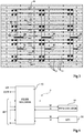
- the figure 3 schematically shows an integrated circuit equipped with an embodiment of a laser attack detection architecture as shown in figure 2 .
- FIG. 3 there is schematically and horizontally illustrated the alternating succession of P-type wells 12 and of N-type wells 14 in which the logic transistors are formed. This representation is very schematic and simply illustrates that the protection architecture is integrated into the logic zone of the integrated circuit.
- the figure 3 arbitrarily represent the case of a matrix network of three columns and four rows of groups of four flip-flops 42 each.
- the architecture, or detection device, shown therefore comprises six gates 46 (two per column) and eight gates 44 (two per row).
- the figure 4 represents, schematically and in the form of blocks, an embodiment of a circuit 5 for interpreting signals supplied by the architecture of the figures 2 and 3 .
- Circuit 5 comprises a state machine, preferably a state machine 52 (STATE MACHINE) in wired logic or a programmable logic network (FPGA), whose inputs IN are individually connected to the respective outputs of the gates 44 and 46 of protection architecture ( figure 3 ).
- Circuit 5 also includes a counter 54 (NVM COUNTER) in non-volatile memory and a delay line 56.
- the counter 54 is written W and read R by the state machine 52.
- the delay line is activated W and its state (active or expired delay) is read R by the state machine 52.
- Circuit 5 also includes an EN activation input which makes it possible, if necessary, to activate / deactivate the protection according to the phases of use of the device. , and an output OUT providing a signal indicative of a detected attack.
- circuit 5 more precisely of its state machine 52, is as follows.
- the state machine 52 increments the counter 54 and activates the delay line 56.
- the state machine determines whether the tilting comes from a rocker close to the previous one. If so, the counter 54 is incremented again and the delay line 56 is also activated again, i.e. the time constant is reset.
- the interpretation of the counter is made by the state machine 52 which periodically compares the state of the counter 54 with a threshold. As soon as the threshold is reached, the presence of an attack is considered and the state machine 52 switches the state of its output OUT.
- the choice of the distance from the neighborhood taken into account depends on the granularity of the groups of rockers in the circuit and on the expected speed of a laser scanning.
- the choice of the time constant of the delay line 56 also depends on the granularity of the groups of flip-flops in the circuit and on the expected speed of a laser scan.
- the triggering threshold of the alarm that is to say the threshold from which the output OUT switches depends on the applications. For example, we choose a threshold between 2 and 10.
- the reaction of the integrated circuit to a switching of the output OUT preferably consists in blocking the circuit and not in a simple restart. Indeed, if a scanning is detected, it is certain that the circuit will then be attacked by laser. with a targeted attack. It is therefore necessary to prevent any further operation. For example, we activate a fuse in non-volatile memory which permanently blocks the circuit.
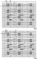
- the figures 5, 6 and 7 illustrate, by schematic views of an integrated circuit embodiment, its operation in the presence of different laser drive modes.
- the figure 5 illustrates the case of a sweep spaced by an interval greater than the interval between two flip-flops 42 of a group.
- the laser beam 34 will touch a first latch of a group but not the next latch of the same group.
- this beam during the scan will statistically inevitably affect a flip-flop of a following group, or even one of the logic gates 56 of the row. If the configuration of the state machine 52 is such that it takes the neighboring column into account, by arbitrarily assuming in this example a threshold of 2 for the counter, the sweep attack is detected.
- the figure 6 illustrates the case of continuous scanning, that is to say in which the laser spots touch each other.
- the triggering will take place from the first group of flip-flops 42 crossed by the sweep.
- the figure 7 illustrates the case of a skew sweep, that is, the case where the sweep is not parallel to the rows or columns of the matrix arrangement. Nevertheless, the laser spots 34 will statistically still reach several flip-flops 42 or gates 44 or 46. Therefore, the scanning is also detected here.
- each group of flip-flops comprises nine flip-flops in a 3x3 matrix arrangement rather than 4 flip-flops in a 2x2 matrix arrangement.
- the flip-flops 42 have been shown but not their connections, nor the rest of the architecture.
- An advantage of the embodiments described is that, unlike the usual systems, there is no reaction. immediate in the presence of a tilting of a detection element (a rocker). Thus, a hacker does not realize, while performing his scan, that he has hit a detector.
- One advantage of the embodiments described is that the risk of taking accidental radiation into account is very low. Indeed, such radiations will touch the circuit at random positions and, consequently, will not trigger the threshold.
Landscapes
- Engineering & Computer Science (AREA)
- Physics & Mathematics (AREA)
- Computer Hardware Design (AREA)
- Mathematical Physics (AREA)
- General Engineering & Computer Science (AREA)
- Computer Security & Cryptography (AREA)
- Theoretical Computer Science (AREA)
- Computing Systems (AREA)
- General Physics & Mathematics (AREA)
- Software Systems (AREA)
- Microelectronics & Electronic Packaging (AREA)
- Computer Networks & Wireless Communication (AREA)
- Signal Processing (AREA)
- Semiconductor Integrated Circuits (AREA)
- Design And Manufacture Of Integrated Circuits (AREA)
- Storage Device Security (AREA)
- Tests Of Electronic Circuits (AREA)
Description
- La présente description concerne de façon générale les circuits électroniques et, plus particulièrement, la protection d'un circuit intégré contre des injections de fautes par attaque laser.
- Dans de nombreuses applications, des circuits électroniques manipulent des données, dites secrètes, c'est-à-dire dont on souhaite réserver l'accès à certains utilisateurs ou circuits.
- De nombreuses méthodes, dites attaques, existent pour tenter de découvrir ou pirater les données secrètes. Parmi ces attaques, des attaques dites par injection de fautes consistent à perturber le fonctionnement du circuit en intervenant sur un ou plusieurs bits qu'il manipule. Une catégorie d'attaques par injection de fautes que vise plus particulièrement la présente description concerne les attaques laser qui consistent à pointer un faisceau laser sur des éléments logiques du circuit afin de faire basculer les bits traités par ces éléments. L'examen de la conséquence de cette attaque sur le comportement du circuit, que ce soit par examen direct des données fournies par le circuit ou par examen indirect en exécutant une analyse par canaux cachés peuvent permettre à l'attaquant de percer un secret.
- Les attaques laser sont généralement des attaques effectuées depuis la face arrière du circuit intégré après un traitement consistant à éroder le substrat.
- Pour contrer ce genre d'attaques, les circuits intégrés sont généralement équipés de détecteurs sous la forme de réseaux de conducteurs (grillage) ou de détecteurs de photocourant ou de courant. Une autre catégorie de détecteurs que vise plus particulièrement la présente description consiste à disposer des éléments logiques de type bascules dont la seule fonction est de détecter un changement d'état représentatif d'une perturbation accidentelle ou volontaire.
- Le document
EP-A-1993057 décrit un procédé et un circuit de détection d'une perturbation d'état d'une bascule d'un circuit électronique. - Le document
WO2008/084016 décrit un procédé et un circuit de protection d'informations contenues dans un circuit électronique. - Le document
US2007/182575 décrit un détecteur pour détecter une manipulation externe d'un circuit électrique. - Le document
WO03/102510 - Il existe un besoin d'améliorer la protection des circuits intégrés contre des attaques laser.
- Un mode de réalisation pallie tout ou partie des inconvénients des techniques usuelles de protection contre des attaques laser.
- Un mode de réalisation propose une solution particulièrement adaptée à des attaques laser se focalisant sur des régions particulières du circuit.
- Un mode de réalisation propose une solution pour détecter une attaque laser avant qu'elle ne se produise sur un élément sensible du point de vue de la sécurité des données qu'il manipule.
- Ainsi, un mode de réalisation prévoit un dispositif de protection d'un circuit intégré selon la revendication 1.
- Selon un mode de réalisation, en présence d'un évènement détecté par un élément de détection, alors que le compteur est dans une valeur initiale, ladite machine d'états incrémente ledit compteur.
- Selon un mode de réalisation, ledit compteur est réinitialisé à l'issue de la temporisation.
- Selon un mode de réalisation, les éléments de détection sont des bascules.
- Selon un mode de réalisation, les portes logiques sont de type OU.
- Un mode de réalisation prévoit un circuit intégré comportant un dispositif de protection.
- Ces caractéristiques et avantages, ainsi que d'autres, seront exposés en détail dans la description suivante de modes de réalisation particuliers faite à titre non limitatif en relation avec les figures jointes parmi lesquelles :
- la
figure 1 est une vue arrière schématique d'un circuit intégré illustrant l'état de la technique et le problème posé ; - la
figure 2 représente, de façon schématique et partielle, un mode de réalisation d'une architecture de détection d'attaque laser ; - la
figure 3 représente, de façon schématique, un circuit intégré équipé d'un mode de réalisation d'une architecture de détection d'attaque laser ; - la
figure 4 représente, de façon schématique et sous forme de blocs, un mode de réalisation d'un circuit d'interprétation de signaux fournis par l'architecture de lafigure 2 ; - les
figures 5, 6 et7 illustrent, par des vues schématiques d'un mode de réalisation de circuit intégré, son fonctionnement en présence de différents modes d'attaque laser ; et - la
figure 8 représente, de façon schématique et partielle, une variante de l'architecture de détection d'attaque laser. - De mêmes éléments ont été désignés par de mêmes références aux différentes figures. En particulier, les éléments structurels et/ou fonctionnels communs aux différents modes de réalisation peuvent présenter les mêmes références et peuvent disposer de propriétés structurelles, dimensionnelles et matérielles identiques. Par souci de clarté, seuls les éléments utiles à la compréhension des modes de réalisation décrits ont été représentés et seront détaillés. En particulier, les fonctions que l'on souhaite protéger, qu'il s'agisse de données proprement dites ou d'algorithmes exécutés, ou celles des circuits électroniques les exécutant n'ont pas été détaillées, les modes de réalisation décrits étant compatibles avec les applications usuelles.
- La
figure 1 est une vue arrière schématique d'un circuit intégré 1 illustrant l'état de la technique et le problème posé. La représentation de lafigure 1 est très schématique et ne représente que partiellement le circuit. - Le circuit 1 est équipé de détecteurs 2 de fautes régulièrement répartis dans sa surface, au moins dans les zones sensibles du point de vue de la sécurité des données manipulées. Chaque détecteur 2 est typiquement une bascule, par exemple une bascule D dont l'état va être modifié par l'arrivée d'un rayonnement depuis la face arrière. Toutes les bascules sont reliées à un circuit d'analyse qui déclenche une contre-mesure, par exemple une réinitialisation du circuit, à la moindre perturbation détectée.
- L'implantation de détecteurs de ce type prend forcément de la place dans le circuit 1 et ils sont donc répartis avec un intervalle fonction de la précision de détection souhaitée.
- Par le passé, les faisceaux laser utilisés présentaient un diamètre de faisceau (spot) 32 tel que le faisceau touchait forcément un des détecteurs lors d'une attaque. Toutefois, les attaques laser s'effectuent désormais avec des faisceaux plus focalisés et donc avec un diamètre d'impact nettement plus petit sur le circuit. Ces nouvelles attaques permettent de contourner certaines contremesures.
- En particulier, une attaque laser commence désormais généralement par un balayage de la face arrière du circuit 1 afin de déterminer les positions des détecteurs. En effet, grâce à la finesse du faisceau 34, en balayant le circuit, on va alterner les instants où le circuit réagit, c'est-à-dire que l'on a touché un détecteur, et les instants où le circuit ne réagit pas. Cela permet à l'attaquant d'effectuer une cartographie des détecteurs pour ensuite focaliser son attaque sur des zones non protégées dans lesquelles il peut injecter des fautes.
- On aurait pu penser accroitre le nombre de détecteurs. Toutefois, il arrive un moment où cela n'est plus possible car il n'y aurait alors plus de place pour les éléments utiles du circuit.
- Par ailleurs, la focalisation des faisceaux laser devient telle qu'un détecteur est incapable de distinguer un photon provenant d'un laser d'une particule alpha provenant, par exemple, du rayonnement cosmique.
- Selon les modes de réalisation décrits, on prévoit d'intégrer, dans le circuit, des réseaux ou groupes de détecteurs de rayonnement sous la forme de réseaux ou groupes de bascules. Par ailleurs, on prévoit préférentiellement une interprétation particulière des signaux de ces bascules prenant en compte un aspect temporel.
- Le rôle du dispositif de détection décrit est de détecter un balayage laser du circuit qui constitue généralement l'étape préalable à une attaque laser proprement dite. Ainsi, on détecte l'attaque avant qu'elle ne soit exploitée sur un des composants sensibles du point de vue de la sécurité des données manipulées.
- La
figure 2 représente, de façon schématique et partielle, un mode de réalisation d'une architecture 4 de détection d'attaque laser. - Selon ce mode de réalisation, on prévoit d'intégrer, à intervalles de préférence réguliers dans le circuit à protéger, des groupes de bascules 42, par exemple de quatre bascules 42, disposées en matrice. Chaque bascule 42 est, par exemple, une bascule D dont l'entrée de donnée est à la masse et dont la sortie directe Q est reliée à deux entrées de deux portes logiques 44 et 46 de type OU. Chaque porte logique 44 reçoit en entrée les signaux des bascules d'une ligne donnée. Chaque porte logique 46 reçoit les signaux des bascules d'une colonne donnée. Ainsi, chaque bascule 42 est reliée à une porte 44 combinant les signaux des bascules de la ligne et à une porte 46 combinant les signaux des bascules de la colonne.
- La
figure 3 représente, de façon schématique, un circuit intégré équipé d'un mode de réalisation d'une architecture de détection d'attaque laser telle que représentée enfigure 2 . - Dans l'exemple de la
figure 3 , on a illustré schématiquement et horizontalement la succession alternée de caissons 12 de type P et de caissons 14 de type N dans lesquels sont formés les transistors logiques. Cette représentation est très schématique et illustre simplement que l'architecture de protection est intégrée dans la zone logique du circuit intégré. - La
figure 3 représente arbitrairement le cas d'un réseau matriciel de trois colonnes et quatre lignes de groupes de quatre bascules 42 chacun. L'architecture, ou dispositif de détection, représenté comporte donc six portes 46 (deux par colonne) et huit portes 44 (deux par ligne). - Lorsque le circuit est alimenté, toutes les bascules sont dans un état de repos à 0. Si une des bascules est frappée par un faisceau laser, son état de sortie va changer et faire basculer la sortie des deux portes 44 et 46 auxquelles est reliée sa sortie Q.
- La
figure 4 représente, de façon schématique et sous forme de blocs, un mode de réalisation d'un circuit 5 d'interprétation de signaux fournis par l'architecture desfigures 2 et3 . - Le circuit 5 comporte une machine d'états, de préférence une machine d'états 52 (STATE MACHINE) en logique câblée ou un réseau logique programmable (FPGA), dont des entrées IN sont individuellement reliées aux sorties respectives des portes 44 et 46 de l'architecture de protection (
figure 3 ). Le circuit 5 comporte également un compteur 54 (NVM COUNTER) en mémoire non volatile et une ligne à retard 56. Le compteur 54 est écrit W et lu R par la machine d'états 52. La ligne à retard est activée W et son état (retard actif ou expiré) est lu R par la machine d'états 52. Le circuit 5 comporte en outre une entrée EN d'activation qui permet, si besoin, d'activer/désactiver la protection selon les phases d'utilisation du dispositif, et une sortie OUT fournissant un signal indicateur d'une attaque détectée. - Le fonctionnement du circuit 5, plus précisément de sa machine d'états 52 est le suivant.
- Au repos, la machine d'états 52 est en attente d'un basculement d'une de ses entrées IN. On suppose le compteur 54 à zéro et la ligne à retard inactive.
- A l'apparition d'un changement d'état d'une entrée IN, la machine d'états 52 incrémente le compteur 54 et active la ligne à retard 56.
- Tant que la ligne à retard est active, c'est-à-dire que sa constante de temps n'est pas expirée, si un autre changement d'état d'une des entrées IN apparait, la machine d'états détermine si le basculement provient d'une bascule voisine de la précédente. Dans l'affirmative, le compteur 54 est incrémenté de nouveau et la ligne à retard 56 est également de nouveau activée, c'est-à-dire que la constante de temps est réinitialisée.
- L'interprétation du compteur est faite par la machine d'états 52 qui compare périodiquement l'état du compteur 54 à un seuil. Dès que le seuil est atteint, on considère la présence d'une attaque et la machine d'états 52 bascule l'état de sa sortie OUT.
- Une fois que la constante de temps de la ligne à retard 56 est écoulée et qu'aucun changement d'état n'est intervenu, le compteur 54 est réinitialisé.
- La prise en compte de la localisation de l'événement dans le réseau matriciel pour déterminer si un évènement suivant intervient à proximité permet de distinguer un balayage laser de particules alpha atteignant le circuit de façon aléatoire.
- Le choix de la distance du voisinage pris en compte (bascules du même groupe, colonnes suivantes et précédentes, lignes et colonnes suivantes et précédentes, etc.) dépend de la granularité des groupes de bascules dans le circuit et de la vitesse attendue d'un balayage laser.
- Le choix de la constante de temps de la ligne à retard 56 dépend également de la granularité des groupes de bascules dans le circuit et de la vitesse attendue d'un balayage laser.
- Le seuil de déclenchement de l'alarme, c'est-à-dire le seuil à partir duquel la sortie OUT bascule dépend des applications. Par exemple, on choisit un seuil compris entre 2 et 10.
- La réaction du circuit intégré à un basculement de la sortie OUT consiste de préférence en un blocage du circuit et non en un simple redémarrage. En effet, si l'on détecte un balayage, on est certain que le circuit va ensuite être attaqué par laser avec une attaque ciblée. Il faut donc empêcher tout fonctionnement ultérieur. Par exemple, on active un fusible en mémoire non volatile qui bloque définitivement le circuit.
- Les
figures 5, 6 et7 illustrent, par des vues schématiques d'un mode de réalisation de circuit intégré, son fonctionnement en présence de différents modes d'attaque laser. - La
figure 5 illustre le cas d'un balayage espacé d'un intervalle supérieur à l'intervalle entre deux bascules 42 d'un groupe. Ainsi, le faisceau laser 34 va toucher une première bascule d'un groupe mais pas la bascule suivante du même groupe. Toutefois, ce faisceau, lors du balayage va statistiquement forcément toucher une bascule d'un groupe suivant, voire une des portes logique 56 de la ligne. Si la configuration de la machine d'états 52 est telle qu'elle tient compte de la colonne voisine, en supposant arbitrairement dans cet exemple un seuil de 2 pour le compteur, l'attaque par balayage est détectée. - La
figure 6 illustre le cas d'un balayage continu, c'est-à-dire dont les spots laser se touchent. Dans ce cas, par exemple avec un seuil de 2 pour le compteur 54, le déclenchement va s'opérer dès le premier groupe de bascules 42 traversé par le balayage. - La
figure 7 illustre le cas d'un balayage en biais, c'est-à-dire dans le cas où le balayage n'est pas parallèle aux lignes ou aux colonnes de l'arrangement matriciel. Néanmoins, les spots laser 34 vont statistiquement quand même atteindre plusieurs bascules 42 ou portes 44 ou 46. Par conséquent, le balayage est ici également détecté. - La
figure 8 représente, de façon schématique et partielle, une variante selon laquelle chaque groupe de bascules comporte neuf bascules en un arrangement matriciel 3x3 plutôt que 4 bascules dans un arrangement matriciel 2x2. Pour simplifier, seules les bascules 42 ont été représentées mais pas leurs connexions, ni le reste de l'architecture. - Un avantage des modes de réalisation décrits est qu'à la différence des systèmes usuels, il n'y a pas de réaction immédiate en présence d'un basculement d'un élément de détection (une bascule). Ainsi, un pirate ne se rend pas compte, en effectuant son balayage qu'il a touché un détecteur.
- Un avantage des modes de réalisation décrits est que le risque de prendre en compte des rayonnements accidentels est très faible. En effet, de tels rayonnements vont toucher le circuit à des positions aléatoires et, par conséquent, ne vont pas déclencher le seuil.
- Divers modes de réalisation ont été décrits. Diverses variantes et modifications, dont l'étendue est uniquement limitée par les revendications, apparaîtront à l'homme de l'art. En particulier, le nombre et la granularité des groupes de bascules de détection dépend de l'application, de la taille du circuit intégré, de la sensibilité souhaitée, etc. En outre, bien que l'on ait pris pour exemple des bascules, les éléments de détection sont plus généralement constitués de tout élément logique sensible à un rayonnement laser. En particulier, les portes logiques 44 et 46 peuvent également constituer des éléments de détection. Enfin, la mise en oeuvre pratique des modes de réalisation qui ont été décrits est à la portée de l'homme du métier à partir des indications fonctionnelles données ci-dessus.
Claims (6)
- Dispositif de protection d'un circuit intégré, comportant :des groupes d'éléments de détection d'un rayonnement (42) répartis dans un arrangement matriciel dans ledit circuit intégré ;des portes logiques (44, 46) combinant des sorties des éléments de détection par ligne et par colonne, chaque sortie d'élément de détection étant reliée à une porte combinant une ligne et à une porte combinant une colonne ; etun circuit (5) d'interprétation des signaux fournis par lesdites portes logiques et comportant un compteur (54) d'événements détectés par un desdits éléments de détection, et un élément de temporisation (56), ledit circuit (5) comportant une machine d'états logiques (52) dont des entrées (IN) sont individuellement reliées aux sorties desdites portes (44, 46),le dispositif étant tel que, en présence d'un événement détecté par un élément de détection (42), ladite machine d'états (52) active l'élément de temporisation (56) et incrémente ledit compteur (54) si l'écart de localisation entre l'événement courant et un événement précédent est inférieur à une distance donnée.
- Dispositif selon la revendication 1, dans lequel, en présence d'un événement détecté par un élément de détection (42), alors que le compteur (54) est dans une valeur initiale, ladite machine d'états (52) incrémente ledit compteur.
- Dispositif selon l'une quelconque des revendications 1 et 2, dans lequel ledit compteur (54) est réinitialisé à l'issue de la temporisation (56).
- Dispositif selon l'une quelconque des revendications 1 à 3, dans lequel les éléments de détection sont des bascules (42) .
- Dispositif selon l'une quelconque des revendications 1 à 4, dans lequel les portes logiques (44, 46) sont de type OU.
- Circuit intégré comportant une architecture de protection selon l'une quelconque des revendications 1 à 5.
Applications Claiming Priority (1)
| Application Number | Priority Date | Filing Date | Title |
|---|---|---|---|
| FR1654371A FR3051599A1 (fr) | 2016-05-17 | 2016-05-17 | Protection d'un circuit integre |
Publications (2)
| Publication Number | Publication Date |
|---|---|
| EP3246944A1 EP3246944A1 (fr) | 2017-11-22 |
| EP3246944B1 true EP3246944B1 (fr) | 2021-03-31 |
Family
ID=56990508
Family Applications (1)
| Application Number | Title | Priority Date | Filing Date |
|---|---|---|---|
| EP16198652.6A Active EP3246944B1 (fr) | 2016-05-17 | 2016-11-14 | Protection d'un circuit intégré |
Country Status (4)
| Country | Link |
|---|---|
| US (2) | US9716502B1 (fr) |
| EP (1) | EP3246944B1 (fr) |
| CN (2) | CN206259946U (fr) |
| FR (1) | FR3051599A1 (fr) |
Families Citing this family (6)
| Publication number | Priority date | Publication date | Assignee | Title |
|---|---|---|---|---|
| FR3051599A1 (fr) * | 2016-05-17 | 2017-11-24 | Stmicroelectronics Rousset | Protection d'un circuit integre |
| FR3054344B1 (fr) * | 2016-07-25 | 2018-09-07 | Tiempo | Circuit integre protege. |
| FR3083051B1 (fr) * | 2018-06-21 | 2023-12-08 | Safran Electronics & Defense | Procede de production d'un circuit optimise pour etre protege contre des radiations |
| US10878133B2 (en) * | 2018-11-18 | 2020-12-29 | Nuvoton Technology Corporation | Mitigation of side-channel attacks using small-overhead random pre-charging |
| US11055409B2 (en) | 2019-01-06 | 2021-07-06 | Nuvoton Technology Corporation | Protected system |
| EP3690867B1 (fr) * | 2019-01-30 | 2025-06-11 | Siemens Aktiengesellschaft | Prise d'empreintes digitales d'agencements de puce à semiconducteur |
Family Cites Families (7)
| Publication number | Priority date | Publication date | Assignee | Title |
|---|---|---|---|---|
| AU2003231894A1 (en) * | 2002-06-04 | 2003-12-19 | Nds Limited | Prevention of tampering in electronic devices |
| DE102005058238B4 (de) * | 2005-12-06 | 2008-08-14 | Infineon Technologies Ag | Detektorschaltung zur Erfassung einer externen Manipulation einer elektrischen Schaltung sowie Verfahren zum Betreiben einer Schaltungsanordnung, bei dem externe Manipulation erfasst werden |
| US8352752B2 (en) * | 2006-09-01 | 2013-01-08 | Inside Secure | Detecting radiation-based attacks |
| EP2108163A1 (fr) * | 2007-01-05 | 2009-10-14 | Proton World International N.V. | Protection d'informations contenues dans un circuit electronique |
| EP1993057B1 (fr) * | 2007-05-18 | 2010-10-20 | STMicroelectronics (Rousset) SAS | Détection d'une perturbation d'état d'une bascule d'un circuit électronique |
| FR2946787A1 (fr) * | 2009-06-16 | 2010-12-17 | St Microelectronics Rousset | Procede de detection d'une attaque par injection de faute d'un dispositif de memoire, et dispositif de memoire correspondant |
| FR3051599A1 (fr) * | 2016-05-17 | 2017-11-24 | Stmicroelectronics Rousset | Protection d'un circuit integre |
-
2016
- 2016-05-17 FR FR1654371A patent/FR3051599A1/fr active Pending
- 2016-11-14 EP EP16198652.6A patent/EP3246944B1/fr active Active
- 2016-11-23 CN CN201621495642.4U patent/CN206259946U/zh not_active Withdrawn - After Issue
- 2016-11-23 CN CN201611271988.0A patent/CN107395189B/zh active Active
- 2016-12-14 US US15/379,155 patent/US9716502B1/en active Active
-
2017
- 2017-06-19 US US15/627,157 patent/US10063239B2/en active Active
Non-Patent Citations (1)
| Title |
|---|
| None * |
Also Published As
| Publication number | Publication date |
|---|---|
| EP3246944A1 (fr) | 2017-11-22 |
| US10063239B2 (en) | 2018-08-28 |
| CN107395189B (zh) | 2020-08-25 |
| FR3051599A1 (fr) | 2017-11-24 |
| CN206259946U (zh) | 2017-06-16 |
| CN107395189A (zh) | 2017-11-24 |
| US9716502B1 (en) | 2017-07-25 |
| US20170338824A1 (en) | 2017-11-23 |
Similar Documents
| Publication | Publication Date | Title |
|---|---|---|
| EP3246944A1 (fr) | Protection d'un circuit intégré | |
| EP2280364B1 (fr) | Détecteur d'injection de fautes dans un circuit intégré | |
| US9117833B2 (en) | Method and device for protecting an integrated circuit against backside attacks | |
| CN101512660B (zh) | 电路装置和电路 | |
| EP2535932B1 (fr) | Puce de circuit intégré comprenant un dispositif de protection contre des attaques | |
| EP1532683B1 (fr) | Prévention d'intervention non autorisée dans des dispositifs électroniques | |
| EP1993057B1 (fr) | Détection d'une perturbation d'état d'une bascule d'un circuit électronique | |
| US20150242624A1 (en) | Memory arrangement and method for detecting an attack on a memory arrangement | |
| FR2998419A1 (fr) | Protection d'un circuit integre contre des attaques | |
| EP3301605B1 (fr) | Puce électronique protégée | |
| WO2023281308A1 (fr) | Matrice de pixels à résolution latérale et temporelle dynamique | |
| EP3674953B1 (fr) | Protection d'un microcontrôleur | |
| WO2013064453A1 (fr) | Procede et dispositif de gestion d'une matrice de touches, avec protection contre un dispositif espion actif, produit programme d'ordinateur et moyen de stockage correspondants | |
| EP3151277B1 (fr) | Circuit intégré sécurisé | |
| US7916517B2 (en) | Circuit arrangement and method for recognizing manipulation attempts | |
| EP2016677B1 (fr) | Composant muni d'un circuit intégré comportant un crypto-processeur et procédé d'installation | |
| US20100025479A1 (en) | Doped Implant Monitoring for Microchip Tamper Detection | |
| EP2680184A1 (fr) | Circuit intégré protégé contre des intrusions d'un pirate | |
| TWI287229B (en) | EEPROM memory matrix and method for safeguarding an EEPROM memory matrix | |
| FR3112004A1 (fr) | Détection d'une impulsion électromagnétique | |
| EP3353767B1 (fr) | Système de détection d'intrusions par reconfiguration | |
| US20100026337A1 (en) | Interdependent Microchip Functionality for Defeating Exploitation Attempts | |
| FR3123468A1 (fr) | Système sur puce | |
| Zooker et al. | Compact sub-Vt optical sensor for the detection of fault injection in hardware security applications | |
| EP3373330B1 (fr) | Architecture de puce électronique |
Legal Events
| Date | Code | Title | Description |
|---|---|---|---|
| PUAI | Public reference made under article 153(3) epc to a published international application that has entered the european phase |
Free format text: ORIGINAL CODE: 0009012 |
|
| STAA | Information on the status of an ep patent application or granted ep patent |
Free format text: STATUS: REQUEST FOR EXAMINATION WAS MADE |
|
| 17P | Request for examination filed |
Effective date: 20161114 |
|
| AK | Designated contracting states |
Kind code of ref document: A1 Designated state(s): AL AT BE BG CH CY CZ DE DK EE ES FI FR GB GR HR HU IE IS IT LI LT LU LV MC MK MT NL NO PL PT RO RS SE SI SK SM TR |
|
| AX | Request for extension of the european patent |
Extension state: BA ME |
|
| STAA | Information on the status of an ep patent application or granted ep patent |
Free format text: STATUS: EXAMINATION IS IN PROGRESS |
|
| 17Q | First examination report despatched |
Effective date: 20200518 |
|
| GRAJ | Information related to disapproval of communication of intention to grant by the applicant or resumption of examination proceedings by the epo deleted |
Free format text: ORIGINAL CODE: EPIDOSDIGR1 |
|
| STAA | Information on the status of an ep patent application or granted ep patent |
Free format text: STATUS: GRANT OF PATENT IS INTENDED |
|
| GRAP | Despatch of communication of intention to grant a patent |
Free format text: ORIGINAL CODE: EPIDOSNIGR1 |
|
| RIC1 | Information provided on ipc code assigned before grant |
Ipc: H03K 19/003 20060101ALI20201130BHEP Ipc: G06F 21/87 20130101ALI20201130BHEP Ipc: G06F 21/75 20130101ALI20201130BHEP Ipc: H03K 19/17704 20200101ALI20201130BHEP Ipc: H01L 23/58 20060101AFI20201130BHEP Ipc: H04L 9/00 20060101ALI20201130BHEP Ipc: H03K 19/17768 20200101ALI20201130BHEP Ipc: G09C 1/00 20060101ALI20201130BHEP |
|
| INTG | Intention to grant announced |
Effective date: 20201221 |
|
| RIN1 | Information on inventor provided before grant (corrected) |
Inventor name: NICOLAS, BRUNO Inventor name: SARAFIANOS, ALEXANDRE |
|
| GRAS | Grant fee paid |
Free format text: ORIGINAL CODE: EPIDOSNIGR3 |
|
| GRAA | (expected) grant |
Free format text: ORIGINAL CODE: 0009210 |
|
| STAA | Information on the status of an ep patent application or granted ep patent |
Free format text: STATUS: THE PATENT HAS BEEN GRANTED |
|
| AK | Designated contracting states |
Kind code of ref document: B1 Designated state(s): AL AT BE BG CH CY CZ DE DK EE ES FI FR GB GR HR HU IE IS IT LI LT LU LV MC MK MT NL NO PL PT RO RS SE SI SK SM TR |
|
| REG | Reference to a national code |
Ref country code: GB Ref legal event code: FG4D Free format text: NOT ENGLISH Ref country code: CH Ref legal event code: EP |
|
| REG | Reference to a national code |
Ref country code: DE Ref legal event code: R096 Ref document number: 602016055149 Country of ref document: DE Ref country code: AT Ref legal event code: REF Ref document number: 1377904 Country of ref document: AT Kind code of ref document: T Effective date: 20210415 |
|
| REG | Reference to a national code |
Ref country code: IE Ref legal event code: FG4D Free format text: LANGUAGE OF EP DOCUMENT: FRENCH |
|
| REG | Reference to a national code |
Ref country code: LT Ref legal event code: MG9D |
|
| PG25 | Lapsed in a contracting state [announced via postgrant information from national office to epo] |
Ref country code: HR Free format text: LAPSE BECAUSE OF FAILURE TO SUBMIT A TRANSLATION OF THE DESCRIPTION OR TO PAY THE FEE WITHIN THE PRESCRIBED TIME-LIMIT Effective date: 20210331 Ref country code: FI Free format text: LAPSE BECAUSE OF FAILURE TO SUBMIT A TRANSLATION OF THE DESCRIPTION OR TO PAY THE FEE WITHIN THE PRESCRIBED TIME-LIMIT Effective date: 20210331 Ref country code: NO Free format text: LAPSE BECAUSE OF FAILURE TO SUBMIT A TRANSLATION OF THE DESCRIPTION OR TO PAY THE FEE WITHIN THE PRESCRIBED TIME-LIMIT Effective date: 20210630 Ref country code: BG Free format text: LAPSE BECAUSE OF FAILURE TO SUBMIT A TRANSLATION OF THE DESCRIPTION OR TO PAY THE FEE WITHIN THE PRESCRIBED TIME-LIMIT Effective date: 20210630 |
|
| PG25 | Lapsed in a contracting state [announced via postgrant information from national office to epo] |
Ref country code: LV Free format text: LAPSE BECAUSE OF FAILURE TO SUBMIT A TRANSLATION OF THE DESCRIPTION OR TO PAY THE FEE WITHIN THE PRESCRIBED TIME-LIMIT Effective date: 20210331 Ref country code: RS Free format text: LAPSE BECAUSE OF FAILURE TO SUBMIT A TRANSLATION OF THE DESCRIPTION OR TO PAY THE FEE WITHIN THE PRESCRIBED TIME-LIMIT Effective date: 20210331 Ref country code: SE Free format text: LAPSE BECAUSE OF FAILURE TO SUBMIT A TRANSLATION OF THE DESCRIPTION OR TO PAY THE FEE WITHIN THE PRESCRIBED TIME-LIMIT Effective date: 20210331 |
|
| REG | Reference to a national code |
Ref country code: NL Ref legal event code: MP Effective date: 20210331 |
|
| REG | Reference to a national code |
Ref country code: AT Ref legal event code: MK05 Ref document number: 1377904 Country of ref document: AT Kind code of ref document: T Effective date: 20210331 |
|
| PG25 | Lapsed in a contracting state [announced via postgrant information from national office to epo] |
Ref country code: AT Free format text: LAPSE BECAUSE OF FAILURE TO SUBMIT A TRANSLATION OF THE DESCRIPTION OR TO PAY THE FEE WITHIN THE PRESCRIBED TIME-LIMIT Effective date: 20210331 Ref country code: SM Free format text: LAPSE BECAUSE OF FAILURE TO SUBMIT A TRANSLATION OF THE DESCRIPTION OR TO PAY THE FEE WITHIN THE PRESCRIBED TIME-LIMIT Effective date: 20210331 Ref country code: EE Free format text: LAPSE BECAUSE OF FAILURE TO SUBMIT A TRANSLATION OF THE DESCRIPTION OR TO PAY THE FEE WITHIN THE PRESCRIBED TIME-LIMIT Effective date: 20210331 Ref country code: CZ Free format text: LAPSE BECAUSE OF FAILURE TO SUBMIT A TRANSLATION OF THE DESCRIPTION OR TO PAY THE FEE WITHIN THE PRESCRIBED TIME-LIMIT Effective date: 20210331 Ref country code: LT Free format text: LAPSE BECAUSE OF FAILURE TO SUBMIT A TRANSLATION OF THE DESCRIPTION OR TO PAY THE FEE WITHIN THE PRESCRIBED TIME-LIMIT Effective date: 20210331 Ref country code: NL Free format text: LAPSE BECAUSE OF FAILURE TO SUBMIT A TRANSLATION OF THE DESCRIPTION OR TO PAY THE FEE WITHIN THE PRESCRIBED TIME-LIMIT Effective date: 20210331 |
|
| PG25 | Lapsed in a contracting state [announced via postgrant information from national office to epo] |
Ref country code: RO Free format text: LAPSE BECAUSE OF FAILURE TO SUBMIT A TRANSLATION OF THE DESCRIPTION OR TO PAY THE FEE WITHIN THE PRESCRIBED TIME-LIMIT Effective date: 20210331 Ref country code: SK Free format text: LAPSE BECAUSE OF FAILURE TO SUBMIT A TRANSLATION OF THE DESCRIPTION OR TO PAY THE FEE WITHIN THE PRESCRIBED TIME-LIMIT Effective date: 20210331 Ref country code: PL Free format text: LAPSE BECAUSE OF FAILURE TO SUBMIT A TRANSLATION OF THE DESCRIPTION OR TO PAY THE FEE WITHIN THE PRESCRIBED TIME-LIMIT Effective date: 20210331 Ref country code: PT Free format text: LAPSE BECAUSE OF FAILURE TO SUBMIT A TRANSLATION OF THE DESCRIPTION OR TO PAY THE FEE WITHIN THE PRESCRIBED TIME-LIMIT Effective date: 20210802 Ref country code: IS Free format text: LAPSE BECAUSE OF FAILURE TO SUBMIT A TRANSLATION OF THE DESCRIPTION OR TO PAY THE FEE WITHIN THE PRESCRIBED TIME-LIMIT Effective date: 20210731 |
|
| REG | Reference to a national code |
Ref country code: DE Ref legal event code: R097 Ref document number: 602016055149 Country of ref document: DE |
|
| PG25 | Lapsed in a contracting state [announced via postgrant information from national office to epo] |
Ref country code: DK Free format text: LAPSE BECAUSE OF FAILURE TO SUBMIT A TRANSLATION OF THE DESCRIPTION OR TO PAY THE FEE WITHIN THE PRESCRIBED TIME-LIMIT Effective date: 20210331 Ref country code: AL Free format text: LAPSE BECAUSE OF FAILURE TO SUBMIT A TRANSLATION OF THE DESCRIPTION OR TO PAY THE FEE WITHIN THE PRESCRIBED TIME-LIMIT Effective date: 20210331 Ref country code: ES Free format text: LAPSE BECAUSE OF FAILURE TO SUBMIT A TRANSLATION OF THE DESCRIPTION OR TO PAY THE FEE WITHIN THE PRESCRIBED TIME-LIMIT Effective date: 20210331 |
|
| PLBE | No opposition filed within time limit |
Free format text: ORIGINAL CODE: 0009261 |
|
| STAA | Information on the status of an ep patent application or granted ep patent |
Free format text: STATUS: NO OPPOSITION FILED WITHIN TIME LIMIT |
|
| 26N | No opposition filed |
Effective date: 20220104 |
|
| PG25 | Lapsed in a contracting state [announced via postgrant information from national office to epo] |
Ref country code: IS Free format text: LAPSE BECAUSE OF FAILURE TO SUBMIT A TRANSLATION OF THE DESCRIPTION OR TO PAY THE FEE WITHIN THE PRESCRIBED TIME-LIMIT Effective date: 20210731 |
|
| PG25 | Lapsed in a contracting state [announced via postgrant information from national office to epo] |
Ref country code: MC Free format text: LAPSE BECAUSE OF FAILURE TO SUBMIT A TRANSLATION OF THE DESCRIPTION OR TO PAY THE FEE WITHIN THE PRESCRIBED TIME-LIMIT Effective date: 20210331 |
|
| REG | Reference to a national code |
Ref country code: CH Ref legal event code: PL |
|
| GBPC | Gb: european patent ceased through non-payment of renewal fee |
Effective date: 20211114 |
|
| PG25 | Lapsed in a contracting state [announced via postgrant information from national office to epo] |
Ref country code: LU Free format text: LAPSE BECAUSE OF NON-PAYMENT OF DUE FEES Effective date: 20211114 Ref country code: IT Free format text: LAPSE BECAUSE OF FAILURE TO SUBMIT A TRANSLATION OF THE DESCRIPTION OR TO PAY THE FEE WITHIN THE PRESCRIBED TIME-LIMIT Effective date: 20210331 Ref country code: BE Free format text: LAPSE BECAUSE OF NON-PAYMENT OF DUE FEES Effective date: 20211130 |
|
| REG | Reference to a national code |
Ref country code: BE Ref legal event code: MM Effective date: 20211130 |
|
| PG25 | Lapsed in a contracting state [announced via postgrant information from national office to epo] |
Ref country code: IE Free format text: LAPSE BECAUSE OF NON-PAYMENT OF DUE FEES Effective date: 20211114 Ref country code: GB Free format text: LAPSE BECAUSE OF NON-PAYMENT OF DUE FEES Effective date: 20211114 |
|
| PG25 | Lapsed in a contracting state [announced via postgrant information from national office to epo] |
Ref country code: FR Free format text: LAPSE BECAUSE OF NON-PAYMENT OF DUE FEES Effective date: 20211130 |
|
| PG25 | Lapsed in a contracting state [announced via postgrant information from national office to epo] |
Ref country code: HU Free format text: LAPSE BECAUSE OF FAILURE TO SUBMIT A TRANSLATION OF THE DESCRIPTION OR TO PAY THE FEE WITHIN THE PRESCRIBED TIME-LIMIT; INVALID AB INITIO Effective date: 20161114 |
|
| PG25 | Lapsed in a contracting state [announced via postgrant information from national office to epo] |
Ref country code: CY Free format text: LAPSE BECAUSE OF FAILURE TO SUBMIT A TRANSLATION OF THE DESCRIPTION OR TO PAY THE FEE WITHIN THE PRESCRIBED TIME-LIMIT Effective date: 20210331 |
|
| PG25 | Lapsed in a contracting state [announced via postgrant information from national office to epo] |
Ref country code: LI Free format text: LAPSE BECAUSE OF NON-PAYMENT OF DUE FEES Effective date: 20220701 Ref country code: GR Free format text: LAPSE BECAUSE OF FAILURE TO SUBMIT A TRANSLATION OF THE DESCRIPTION OR TO PAY THE FEE WITHIN THE PRESCRIBED TIME-LIMIT Effective date: 20210331 Ref country code: CH Free format text: LAPSE BECAUSE OF NON-PAYMENT OF DUE FEES Effective date: 20220701 |
|
| PG25 | Lapsed in a contracting state [announced via postgrant information from national office to epo] |
Ref country code: MK Free format text: LAPSE BECAUSE OF FAILURE TO SUBMIT A TRANSLATION OF THE DESCRIPTION OR TO PAY THE FEE WITHIN THE PRESCRIBED TIME-LIMIT Effective date: 20210331 |
|
| PG25 | Lapsed in a contracting state [announced via postgrant information from national office to epo] |
Ref country code: MT Free format text: LAPSE BECAUSE OF FAILURE TO SUBMIT A TRANSLATION OF THE DESCRIPTION OR TO PAY THE FEE WITHIN THE PRESCRIBED TIME-LIMIT Effective date: 20210331 |
|
| REG | Reference to a national code |
Ref country code: DE Ref legal event code: R079 Ref document number: 602016055149 Country of ref document: DE Free format text: PREVIOUS MAIN CLASS: H01L0023580000 Ipc: H10W0029000000 |
|
| PG25 | Lapsed in a contracting state [announced via postgrant information from national office to epo] |
Ref country code: TR Free format text: LAPSE BECAUSE OF FAILURE TO SUBMIT A TRANSLATION OF THE DESCRIPTION OR TO PAY THE FEE WITHIN THE PRESCRIBED TIME-LIMIT Effective date: 20210331 |
|
| PGFP | Annual fee paid to national office [announced via postgrant information from national office to epo] |
Ref country code: DE Payment date: 20251022 Year of fee payment: 10 |