EP3244603A1 - Imaging unit, imaging module and endoscopic system - Google Patents
Imaging unit, imaging module and endoscopic system Download PDFInfo
- Publication number
- EP3244603A1 EP3244603A1 EP15876948.9A EP15876948A EP3244603A1 EP 3244603 A1 EP3244603 A1 EP 3244603A1 EP 15876948 A EP15876948 A EP 15876948A EP 3244603 A1 EP3244603 A1 EP 3244603A1
- Authority
- EP
- European Patent Office
- Prior art keywords
- layer substrate
- imaging unit
- layer
- semiconductor package
- substrate
- Prior art date
- Legal status (The legal status is an assumption and is not a legal conclusion. Google has not performed a legal analysis and makes no representation as to the accuracy of the status listed.)
- Withdrawn
Links
Images



Classifications
-
- H—ELECTRICITY
- H10—SEMICONDUCTOR DEVICES; ELECTRIC SOLID-STATE DEVICES NOT OTHERWISE PROVIDED FOR
- H10F—INORGANIC SEMICONDUCTOR DEVICES SENSITIVE TO INFRARED RADIATION, LIGHT, ELECTROMAGNETIC RADIATION OF SHORTER WAVELENGTH OR CORPUSCULAR RADIATION
- H10F39/00—Integrated devices, or assemblies of multiple devices, comprising at least one element covered by group H10F30/00, e.g. radiation detectors comprising photodiode arrays
- H10F39/80—Constructional details of image sensors
- H10F39/804—Containers or encapsulations
-
- A—HUMAN NECESSITIES
- A61—MEDICAL OR VETERINARY SCIENCE; HYGIENE
- A61B—DIAGNOSIS; SURGERY; IDENTIFICATION
- A61B1/00—Instruments for performing medical examinations of the interior of cavities or tubes of the body by visual or photographical inspection, e.g. endoscopes; Illuminating arrangements therefor
- A61B1/00002—Operational features of endoscopes
- A61B1/00043—Operational features of endoscopes provided with output arrangements
- A61B1/00045—Display arrangement
-
- A—HUMAN NECESSITIES
- A61—MEDICAL OR VETERINARY SCIENCE; HYGIENE
- A61B—DIAGNOSIS; SURGERY; IDENTIFICATION
- A61B1/00—Instruments for performing medical examinations of the interior of cavities or tubes of the body by visual or photographical inspection, e.g. endoscopes; Illuminating arrangements therefor
- A61B1/04—Instruments for performing medical examinations of the interior of cavities or tubes of the body by visual or photographical inspection, e.g. endoscopes; Illuminating arrangements therefor combined with photographic or television appliances
- A61B1/044—Instruments for performing medical examinations of the interior of cavities or tubes of the body by visual or photographical inspection, e.g. endoscopes; Illuminating arrangements therefor combined with photographic or television appliances for absorption imaging
-
- A—HUMAN NECESSITIES
- A61—MEDICAL OR VETERINARY SCIENCE; HYGIENE
- A61B—DIAGNOSIS; SURGERY; IDENTIFICATION
- A61B1/00—Instruments for performing medical examinations of the interior of cavities or tubes of the body by visual or photographical inspection, e.g. endoscopes; Illuminating arrangements therefor
- A61B1/04—Instruments for performing medical examinations of the interior of cavities or tubes of the body by visual or photographical inspection, e.g. endoscopes; Illuminating arrangements therefor combined with photographic or television appliances
- A61B1/05—Instruments for performing medical examinations of the interior of cavities or tubes of the body by visual or photographical inspection, e.g. endoscopes; Illuminating arrangements therefor combined with photographic or television appliances characterised by the image sensor, e.g. camera, being in the distal end portion
- A61B1/051—Details of CCD assembly
-
- G—PHYSICS
- G02—OPTICS
- G02B—OPTICAL ELEMENTS, SYSTEMS OR APPARATUS
- G02B23/00—Telescopes, e.g. binoculars; Periscopes; Instruments for viewing the inside of hollow bodies; Viewfinders; Optical aiming or sighting devices
- G02B23/24—Instruments or systems for viewing the inside of hollow bodies, e.g. fibrescopes
- G02B23/2476—Non-optical details, e.g. housings, mountings, supports
- G02B23/2484—Arrangements in relation to a camera or imaging device
-
- H—ELECTRICITY
- H04—ELECTRIC COMMUNICATION TECHNIQUE
- H04N—PICTORIAL COMMUNICATION, e.g. TELEVISION
- H04N23/00—Cameras or camera modules comprising electronic image sensors; Control thereof
- H04N23/56—Cameras or camera modules comprising electronic image sensors; Control thereof provided with illuminating means
-
- H—ELECTRICITY
- H10—SEMICONDUCTOR DEVICES; ELECTRIC SOLID-STATE DEVICES NOT OTHERWISE PROVIDED FOR
- H10F—INORGANIC SEMICONDUCTOR DEVICES SENSITIVE TO INFRARED RADIATION, LIGHT, ELECTROMAGNETIC RADIATION OF SHORTER WAVELENGTH OR CORPUSCULAR RADIATION
- H10F39/00—Integrated devices, or assemblies of multiple devices, comprising at least one element covered by group H10F30/00, e.g. radiation detectors comprising photodiode arrays
- H10F39/10—Integrated devices
- H10F39/12—Image sensors
-
- H—ELECTRICITY
- H10—SEMICONDUCTOR DEVICES; ELECTRIC SOLID-STATE DEVICES NOT OTHERWISE PROVIDED FOR
- H10F—INORGANIC SEMICONDUCTOR DEVICES SENSITIVE TO INFRARED RADIATION, LIGHT, ELECTROMAGNETIC RADIATION OF SHORTER WAVELENGTH OR CORPUSCULAR RADIATION
- H10F39/00—Integrated devices, or assemblies of multiple devices, comprising at least one element covered by group H10F30/00, e.g. radiation detectors comprising photodiode arrays
- H10F39/80—Constructional details of image sensors
- H10F39/809—Constructional details of image sensors of hybrid image sensors
-
- H—ELECTRICITY
- H10—SEMICONDUCTOR DEVICES; ELECTRIC SOLID-STATE DEVICES NOT OTHERWISE PROVIDED FOR
- H10F—INORGANIC SEMICONDUCTOR DEVICES SENSITIVE TO INFRARED RADIATION, LIGHT, ELECTROMAGNETIC RADIATION OF SHORTER WAVELENGTH OR CORPUSCULAR RADIATION
- H10F39/00—Integrated devices, or assemblies of multiple devices, comprising at least one element covered by group H10F30/00, e.g. radiation detectors comprising photodiode arrays
- H10F39/80—Constructional details of image sensors
- H10F39/811—Interconnections
-
- H—ELECTRICITY
- H10—SEMICONDUCTOR DEVICES; ELECTRIC SOLID-STATE DEVICES NOT OTHERWISE PROVIDED FOR
- H10F—INORGANIC SEMICONDUCTOR DEVICES SENSITIVE TO INFRARED RADIATION, LIGHT, ELECTROMAGNETIC RADIATION OF SHORTER WAVELENGTH OR CORPUSCULAR RADIATION
- H10F77/00—Constructional details of devices covered by this subclass
- H10F77/50—Encapsulations or containers
-
- H—ELECTRICITY
- H10—SEMICONDUCTOR DEVICES; ELECTRIC SOLID-STATE DEVICES NOT OTHERWISE PROVIDED FOR
- H10W—GENERIC PACKAGES, INTERCONNECTIONS, CONNECTORS OR OTHER CONSTRUCTIONAL DETAILS OF DEVICES COVERED BY CLASS H10
- H10W70/00—Package substrates; Interposers; Redistribution layers [RDL]
- H10W70/60—Insulating or insulated package substrates; Interposers; Redistribution layers
-
- H—ELECTRICITY
- H10—SEMICONDUCTOR DEVICES; ELECTRIC SOLID-STATE DEVICES NOT OTHERWISE PROVIDED FOR
- H10W—GENERIC PACKAGES, INTERCONNECTIONS, CONNECTORS OR OTHER CONSTRUCTIONAL DETAILS OF DEVICES COVERED BY CLASS H10
- H10W70/00—Package substrates; Interposers; Redistribution layers [RDL]
- H10W70/60—Insulating or insulated package substrates; Interposers; Redistribution layers
- H10W70/611—Insulating or insulated package substrates; Interposers; Redistribution layers for connecting multiple chips together
-
- H—ELECTRICITY
- H10—SEMICONDUCTOR DEVICES; ELECTRIC SOLID-STATE DEVICES NOT OTHERWISE PROVIDED FOR
- H10W—GENERIC PACKAGES, INTERCONNECTIONS, CONNECTORS OR OTHER CONSTRUCTIONAL DETAILS OF DEVICES COVERED BY CLASS H10
- H10W70/00—Package substrates; Interposers; Redistribution layers [RDL]
- H10W70/60—Insulating or insulated package substrates; Interposers; Redistribution layers
- H10W70/62—Insulating or insulated package substrates; Interposers; Redistribution layers characterised by their interconnections
- H10W70/63—Vias, e.g. via plugs
- H10W70/635—Through-vias
-
- H—ELECTRICITY
- H10—SEMICONDUCTOR DEVICES; ELECTRIC SOLID-STATE DEVICES NOT OTHERWISE PROVIDED FOR
- H10W—GENERIC PACKAGES, INTERCONNECTIONS, CONNECTORS OR OTHER CONSTRUCTIONAL DETAILS OF DEVICES COVERED BY CLASS H10
- H10W70/00—Package substrates; Interposers; Redistribution layers [RDL]
- H10W70/60—Insulating or insulated package substrates; Interposers; Redistribution layers
- H10W70/62—Insulating or insulated package substrates; Interposers; Redistribution layers characterised by their interconnections
- H10W70/65—Shapes or dispositions of interconnections
-
- H—ELECTRICITY
- H10—SEMICONDUCTOR DEVICES; ELECTRIC SOLID-STATE DEVICES NOT OTHERWISE PROVIDED FOR
- H10W—GENERIC PACKAGES, INTERCONNECTIONS, CONNECTORS OR OTHER CONSTRUCTIONAL DETAILS OF DEVICES COVERED BY CLASS H10
- H10W70/00—Package substrates; Interposers; Redistribution layers [RDL]
- H10W70/60—Insulating or insulated package substrates; Interposers; Redistribution layers
- H10W70/67—Insulating or insulated package substrates; Interposers; Redistribution layers characterised by their insulating layers or insulating parts
- H10W70/68—Shapes or dispositions thereof
- H10W70/685—Shapes or dispositions thereof comprising multiple insulating layers
-
- H—ELECTRICITY
- H10—SEMICONDUCTOR DEVICES; ELECTRIC SOLID-STATE DEVICES NOT OTHERWISE PROVIDED FOR
- H10W—GENERIC PACKAGES, INTERCONNECTIONS, CONNECTORS OR OTHER CONSTRUCTIONAL DETAILS OF DEVICES COVERED BY CLASS H10
- H10W72/00—Interconnections or connectors in packages
- H10W72/20—Bump connectors, e.g. solder bumps or copper pillars; Dummy bumps; Thermal bumps
-
- H—ELECTRICITY
- H10—SEMICONDUCTOR DEVICES; ELECTRIC SOLID-STATE DEVICES NOT OTHERWISE PROVIDED FOR
- H10W—GENERIC PACKAGES, INTERCONNECTIONS, CONNECTORS OR OTHER CONSTRUCTIONAL DETAILS OF DEVICES COVERED BY CLASS H10
- H10W76/00—Containers; Fillings or auxiliary members therefor; Seals
- H10W76/10—Containers or parts thereof
- H10W76/12—Containers or parts thereof characterised by their shape
- H10W76/15—Containers comprising an insulating or insulated base
-
- H—ELECTRICITY
- H10—SEMICONDUCTOR DEVICES; ELECTRIC SOLID-STATE DEVICES NOT OTHERWISE PROVIDED FOR
- H10W—GENERIC PACKAGES, INTERCONNECTIONS, CONNECTORS OR OTHER CONSTRUCTIONAL DETAILS OF DEVICES COVERED BY CLASS H10
- H10W78/00—Detachable holders for supporting packaged chips in operation
-
- H—ELECTRICITY
- H10—SEMICONDUCTOR DEVICES; ELECTRIC SOLID-STATE DEVICES NOT OTHERWISE PROVIDED FOR
- H10W—GENERIC PACKAGES, INTERCONNECTIONS, CONNECTORS OR OTHER CONSTRUCTIONAL DETAILS OF DEVICES COVERED BY CLASS H10
- H10W90/00—Package configurations
- H10W90/401—Package configurations characterised by multiple insulating or insulated package substrates, interposers or RDLs
-
- H—ELECTRICITY
- H04—ELECTRIC COMMUNICATION TECHNIQUE
- H04N—PICTORIAL COMMUNICATION, e.g. TELEVISION
- H04N23/00—Cameras or camera modules comprising electronic image sensors; Control thereof
- H04N23/50—Constructional details
- H04N23/555—Constructional details for picking-up images in sites, inaccessible due to their dimensions or hazardous conditions, e.g. endoscopes or borescopes
-
- H—ELECTRICITY
- H10—SEMICONDUCTOR DEVICES; ELECTRIC SOLID-STATE DEVICES NOT OTHERWISE PROVIDED FOR
- H10F—INORGANIC SEMICONDUCTOR DEVICES SENSITIVE TO INFRARED RADIATION, LIGHT, ELECTROMAGNETIC RADIATION OF SHORTER WAVELENGTH OR CORPUSCULAR RADIATION
- H10F39/00—Integrated devices, or assemblies of multiple devices, comprising at least one element covered by group H10F30/00, e.g. radiation detectors comprising photodiode arrays
- H10F39/10—Integrated devices
- H10F39/12—Image sensors
- H10F39/199—Back-illuminated image sensors
-
- H—ELECTRICITY
- H10—SEMICONDUCTOR DEVICES; ELECTRIC SOLID-STATE DEVICES NOT OTHERWISE PROVIDED FOR
- H10W—GENERIC PACKAGES, INTERCONNECTIONS, CONNECTORS OR OTHER CONSTRUCTIONAL DETAILS OF DEVICES COVERED BY CLASS H10
- H10W76/00—Containers; Fillings or auxiliary members therefor; Seals
- H10W76/10—Containers or parts thereof
- H10W76/12—Containers or parts thereof characterised by their shape
-
- H—ELECTRICITY
- H10—SEMICONDUCTOR DEVICES; ELECTRIC SOLID-STATE DEVICES NOT OTHERWISE PROVIDED FOR
- H10W—GENERIC PACKAGES, INTERCONNECTIONS, CONNECTORS OR OTHER CONSTRUCTIONAL DETAILS OF DEVICES COVERED BY CLASS H10
- H10W76/00—Containers; Fillings or auxiliary members therefor; Seals
- H10W76/10—Containers or parts thereof
- H10W76/12—Containers or parts thereof characterised by their shape
- H10W76/161—Containers comprising no base
Definitions
- the present invention relates to an imaging unit disposed on a distal end of an insertion section of an endoscope that is configured to be inserted into a subject to image an inside of the subject.
- the present invention also relates to an imaging module and an endoscope system.
- a medical endoscope apparatus is capable of acquiring an in-vivo image inside the body cavity without making an incision on a subject such as a patient by inserting an elongated and flexible insertion section including an image sensor disposed on the distal end thereof into the body cavity of the subject and further capable of performing a therapeutic treatment by allowing a treatment tool to project from the distal end of the insertion section as needed, and thus widely used.
- An imaging unit which includes an image sensor and a circuit board on which electronic components such as a capacitor and an IC chip which constitute a drive circuit for the image sensor are mounted is inserted in the distal end of the insertion section of such an endoscope apparatus, and a signal cable is soldered to the circuit board of the imaging unit.
- an imaging unit that achieves a three-dimensional structure of a circuit board connected to an image sensor for the purpose of simplifying a signal line connecting operation in a cable, improving the reliability of a connected part, or reducing the size.
- Patent Literatures 1 to 5 since an electronic component such as a bypass capacitor is mounted at a position away from an image sensor, the impedance of wiring is increased, which causes low image quality due to generation of noise.
- the present invention has been made in view of the foregoing, and an object of the invention is to provide an imaging unit, an imaging module and an endoscope system that make it possible to achieve a reduced diameter of a distal end of an insertion section and to obtain a high-quality image.
- an imaging unit includes: a semiconductor package having an image sensor and having a connection electrode on a back face of the semiconductor package; a first multi-layer substrate having a plurality of layered substrates and having connection electrodes respectively on a front face and on a back face of the first multi-layer substrate, the connection electrode on the front face being configured to be electrically and mechanically connected to the connection electrode of the semiconductor package; a second multi-layer substrate having a plurality of layered substrates, the second multi-layer substrate being configured to be electrically and mechanically connected to the back face of the first multi-layer substrate such that a layer direction of the second multi-layer substrate is perpendicular to a layer direction of the first multi-layer substrate; an electronic component mounted inside the first multi-layer substrate; and a plurality of cables configured to be electrically and mechanically connected to the second multi-layer substrate.
- the second multi-layer substrate is connected to the back face of the first multi-layer substrate to form a T shape, and the first multi-layer substrate
- a plurality of electronic components is mounted inside the first multi-layer substrate.
- an arrangement region for a plurality of vias connecting the layered substrates and a mounting region for the plurality of electronic components are sectioned so as to be adjacent to each other.
- a plurality of electronic components is mounted inside the first multi-layer substrate.
- the plurality of electronic components is mounted in a central part of the first multi-layer substrate, and a plurality of vias connecting the layered substrates is arranged along an outer periphery of the first multi-layer substrate.
- At least one of the plurality of cables is connected to the via arranged along the outer periphery of the first multi-layer substrate.
- the plurality of cables connected to the second multi-layer substrate is arranged at different positions along the optical axis direction.
- the cable connected to the second multi-layer substrate at a position closer to the first multi-layer substrate is connected to the electronic component mounted inside the first multi-layer substrate.
- the first multi-layer substrate has, on the back face thereof, a recess into which an end part of the second multi-layer substrate is inserted, and the electronic component mounted inside the first multi-layer substrate is arranged at a position different from a position of the recess.
- the second multi-layer substrate is connected to the first multi-layer substrate at a position shifted from a center of the first multi-layer substrate so as to divide the projected plane in the optical axis direction of the image sensor into a wide projected plane and a narrow projected plane by the second multi-layer substrate.
- the cable having a larger outer diameter is connected to a face corresponding to the wide projected plane.
- the cable having a smaller outer diameter is connected to a face corresponding to the narrow projected plane.
- the second multi-layer substrate is connected to the first multi-layer substrate with the second multi-layer substrate inclined with respect to a horizontal direction.
- the first multi-layer substrate, the second multi-layer substrate, and the plurality of cables lie within the projected plane in the optical axis direction of the image sensor.
- An imaging module includes: a semiconductor package having an image sensor and having a connection electrode on a back face of the semiconductor package; a first multi-layer substrate having a plurality of layered substrates and having connection electrodes respectively on a front face and on a back face of the first multi-layer substrate, the connection electrode on the front face being configured to be electrically and mechanically connected to the connection electrode of the semiconductor package; a second multi-layer substrate having a plurality of layered substrates, the second multi-layer substrate being configured to be electrically and mechanically connected to the back face of the first multi-layer substrate such that a layer direction of the second multi-layer substrate is perpendicular to a layer direction of the first multi-layer substrate; and an electronic component mounted inside the first multi-layer substrate.
- the second multi-layer substrate is connected to the back face of the first multi-layer substrate to form a T shape, and the first multi-layer substrate and the second multi-layer substrate lie within a projected plane in an optical axis direction of the semiconductor package.
- An endoscope system includes an insertion section having the imaging unit according to the above-described invention disposed on a distal end of the insertion section.
- an electronic component is mounted inside a first multi-layer substrate adjacent to a semiconductor package.
- FIG. 1 is a diagram schematically illustrating the entire configuration of an endoscope system according to a first embodiment of the present invention.
- the endoscope system 1 according to the first embodiment has an endoscope 2 which is configured to be introduced into a subject and to image the inside of the subject to generate an image signal of the subject, an information processing device 3 which is configured to perform predetermined image processing on the image signal captured by the endoscope 2 and controls each unit of the endoscope system 1, a light source device 4 which is configured to produce illumination light of the endoscope 2, and a display device 5 which is configured to display the image signal after the image processing by the information processing device 3.
- the endoscope 2 includes an insertion section 6 which is configured to be inserted into a subject, an operating unit 7 which is located at the proximal end side of the insertion section 6 and is configured to be grasped by an operator, and a flexible universal cord 8 which extends from the operating unit 7.
- the insertion section 6 is achieved using, for example, an illumination fiber (light guide cable), an electric cable, and an optical fiber.
- the insertion section 6 includes a distal end part 6a which has a built-in imaging unit (described below), a bendable part 6b which includes a plurality of bending pieces so as to be freely bendable, and a flexible tube part 6c which is disposed at the proximal end side of the bendable part 6b.
- the distal end part 6a is provided with an illumination unit which illuminates the inside of a subject through an illumination lens, an observation unit which images the inside of a subject, an opening with which a treatment tool channel communicates, and an air/water feeding nozzle (not illustrated).
- the operating unit 7 includes a bending knob 7a which bends the bendable part 6b in up-down and right-left directions, a treatment tool insertion part 7b from which a treatment tool such as a biopsy forceps or a laser scalpel is inserted into the body cavity of a subject, and a plurality of switches 7c for operating peripheral devices including the information processing device 3, the light source device 4, an air feeding device, a water feeding device, and a gas feeding device.
- a treatment tool inserted from the treatment tool insertion part 7b passes through the treatment tool channel formed inside thereof and is exposed from the opening formed on the distal end of the insertion section 6.
- the universal cord 8 is configured using, for example, an illumination fiber, an electric cable, and an optical fiber.
- the universal cord 8 is branched at the proximal end thereof, and includes a connector 8a on one end of the branched part and a connector 8b on the other proximal end thereof.
- the connector 8a is freely attachable to and detachable from a connector of the information processing device 3.
- the connector 8b is freely attachable to and detachable from the light source device 4.
- the universal cord 8 transmits illumination light emitted from the light source device 4 to the distal end part 6a through the connector 8b and the illumination fiber. Further, the universal cord 8 transmits an image signal captured by the imaging unit (described below) to the information processing device 3 through the cable and the connector 8a.
- the information processing device 3 performs predetermined image processing on an image signal output from the connector 8a and controls the entire endoscope system 1.
- the light source device 4 is configured using, for example, a light source which emits light and a condenser lens.
- the light source device 4 emits light from the light source and supplies the emitted light to the endoscope 2 which is connected through the connector 8b and the illumination fiber of the universal cord 8 as illumination light to the inside of a subject under the control of the information processing device 3.
- the display device 5 is configured using, for example, a display using a liquid crystal or an organic electro luminescence (EL).
- the display device 5 displays various kinds of information including an image on which predetermined image processing has been performed by the information processing device 3 through a video cable 5a. Accordingly, an operator can perform observation and property determination for a desired position inside a subject by operating the endoscope 2 while checking an image (in-vivo image) displayed on the display device 5.
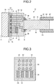
- FIG. 2 is a sectional view of the imaging unit which is disposed on the distal end of the endoscope illustrated in FIG. 1 .
- FIG. 3 is an A-A sectional view of the imaging unit illustrated in FIG. 2 .
- An imaging unit 10 has a semiconductor package 20 which includes an image sensor and a connection electrode 21 formed on the back face thereof, a first multi-layer substrate 30 which has a plate shape and includes a connection electrode 31 formed on the front face thereof and a connection electrode 33 formed on the back face thereof, the connection electrode 31 on the front face being electrically and mechanically connected to the connection electrode 21 of the semiconductor package 20, a second multi-layer substrate 40 which has a plate shape and is electrically and mechanically connected to the back face of the first multi-layer substrate 30 with a layer direction of the second multi-layer substrate 40 perpendicular to a layer direction of the first multi-layer substrate 30, an electronic component 51 mounted inside the first multi-layer substrate 30, and a plurality of cables 60 configured to be electrically and mechanically connected to the second multi-layer substrate 40.
- the image sensor of the semiconductor package 20 includes, for example, a CMOS, and a light receiver which receives light condensed by a lens unit is disposed on a face f1 as the front face.
- the light receiver is connected to the connection electrode 21 formed on a face f2 as the back face.
- a bump 22 which includes, for example, a solder is formed on the connection electrode 21.
- the semiconductor package 20 is preferably a chip size package (CSP) that is formed by performing wiring, electrode forming, resin sealing, and dicing on an image sensor chip in a wafer state so that the image sensor chip finally has a size equal to the size of the semiconductor package.
- CSP chip size package
- the first multi-layer substrate 30 has a plate shape in which a plurality of substrates having wiring is layered (a plurality of substrates parallel to a face f3 and a face f4 is layered). For example, a ceramic substrate, a glass epoxy substrate, a glass substrate, or a silicon substrate is used as each of the layered substrates.
- a plurality of electronic components 51 is built inside the first multi-layer substrate 30, and a plurality of vias 32 for electrically connecting the wiring on the layered substrates is formed inside the first multi-layer substrate 30. As illustrated in FIG. 3 , four electronic components 51 are built into the first multi-layer substrate 30. All the electronic components 51 may be the same kind or different kinds of electronic components, and the number of built-in electronic components 51 is not limited to four. Examples of the electronic component 51 include a capacitor, a passive component such as a resistance coil, and an active component such as a driver IC. Further, the number and the arrangement of vias 32 are not limited to those illustrated in FIG. 3 .
- connection electrode 31 is formed on the face f3 of the first multi-layer substrate 30, and electrically and mechanically connected to the connection electrode 21 of the semiconductor package 20 through the bump 22. A connection part between the connection electrode 31 and the connection electrode 21 is sealed with a sealing resin 23.
- connection electrode 33 is formed on the face f4 of the first multi-layer substrate 30 and connected to the connection electrode 31 through the via 32.
- the electronic components 51 inside the first multi-layer substrate 30 are mounted in an electronic component arrangement region 36 in substrate layers of the first multi-layer substrate 30.
- the electronic component arrangement region 36 is sectioned so as to be adjacent to a via arrangement region 35 in which the vias 32 are arranged.
- the electronic components 51 and the vias 32 can be efficiently arranged within a limited space by sectioning the electronic component arrangement region 36 and the via arrangement region 35 so as to be adjacent to each other.
- the second multi-layer substrate 40 has a plate shape in which a plurality of substrates having wiring is layered (a plurality of substrates parallel to a face f5 and a face f6 is layered) similarly to the first multi-layer substrate 30.
- a ceramic substrate, a glass epoxy substrate, a glass substrate, or a silicon substrate is used as each of the layered substrates.
- the second multi-layer substrate 40 is electrically and mechanically connected to the first multi-layer substrate 30 with the layer direction of the second multi-layer substrate 40 perpendicular to the layer direction of the first multi-layer substrate 30.
- the first multi-layer substrate 30 and the second multi-layer substrate 40 are connected to form a T shape.
- the face f4 which is the back face of the first multi-layer substrate 30 is equally divided into two parts by the second multi-layer substrate 40.
- a connection electrode 41 is formed on one end of the second multi-layer substrate 40 and connected to the connection electrode 33 of the first multi-layer substrate 30 with a solder 34.
- the connection between the first multi-layer substrate 30 and the second multi-layer substrate 40 is performed in such a manner that an adhesive is applied to a predetermined position of the first multi-layer substrate 30, the second multi-layer substrate 40 is then placed and temporarily fixed, and the connection electrode 33 and the connection electrode 41 are then connected with the solder 34.
- a cable connecting electrode 42 for connecting the plurality of cables 60 is formed on the other end of the second multi-layer substrate 40.
- an insulating outer sheath 62 on one end is peeled, and an exposed conductor 61 is connected to the cable connecting electrode 42 with a solder 43.
- the electronic components 51 are built into the first multi-layer substrate 30 which is directly connected to the semiconductor package 20.
- the distance between the electronic components 51 and the image sensor inside the semiconductor package 20 that is, reduce the wiring length to reduce noise.
- wiring reduction is achieved compared to the case in which the electronic components 51 are mounted in the second multi-layer substrate 40. Accordingly, the entire length of the imaging unit can be reduced.
- the first multi-layer substrate 30, the second multi-layer substrate 40, and the plurality of cables 60 lie within a projected plane in an optical axis direction of the semiconductor package 20. It is therefore possible to achieve a reduced diameter of the imaging unit 10.
- FIG. 4 is a sectional view of the imaging unit according to the first modification of the first embodiment of the present invention.
- the second multi-layer substrate 40 is connected to the back face of the first multi-layer substrate 30 at a position shifted downward (toward a face f7 of the first multi-layer substrate 30) from the center thereof. Further, cables 63, 64, 65 and 66 having different outer diameters are connected to the second multi-layer substrate 40.
- the outer diameter of the imaging unit 10A may be increased.
- the second multi-layer substrate 40 is connected to the back face of the first multi-layer substrate 30 at the position shifted from the center thereof so as to divide the projected plane in the optical axis direction of the image sensor into a wide projected plane and a narrow projected plane by the second multi-layer substrate 40, and the cables 63 and 64 having a large outer diameter are connected to a face (the face f5) corresponding to the wide projected plane and the cables 65 and 66 having a small outer diameter are connected to a face (the face f6) corresponding to the narrow projected plane.
- the cables 63 and 64 having a large outer diameter are used, it is possible to allow the first multi-layer substrate 30, the second multi-layer substrate 40, and the cables 63 and 64 to lie within the projected plane in the optical axis direction of the image sensor, thereby to achieve the reduced diameter of the imaging unit 10A.
- the cables 63 to 66 are connected to the second multi-layer substrate 40 at different positions along the optical axis direction.
- the cable 64 is connected at a position closer to the first multi-layer substrate 30, and the cable 63 is connected at the proximal end side.
- the cable 66 is connected at a position closer to the first multi-layer substrate 30, and the cable 65 is connected at the proximal end side.
- the cable 64 which is connected at the position closer to the first multi-layer substrate 30 transmits an electric signal to the semiconductor package 20 through the electronic component 51 mounted inside the first multi-layer substrate 30.
- the electric signal is transmitted from the cable 64 to the semiconductor package 20 as indicated by a solid line in FIG. 4 . Further, an electric signal is transmitted from the cable 63 to the semiconductor package 20 as indicated by a dotted line in FIG. 4 . In FIG. 4 , transmission paths of an electric signal between the cables 65, 66 and the semiconductor package 20 are not illustrated. Noise can be reduced by connecting the cable 64 which is connected to the electronic component 51 mounted inside the first multi-layer substrate 30 at the position closer to the first multi-layer substrate 30.
- FIG. 5 is a side view of the imaging unit according to the second modification of the first embodiment of the present invention.
- FIG. 6 is a diagram describing an arrangement configuration between the second multi-layer substrate and cables of the imaging unit illustrated in FIG. 5 .
- the second multi-layer substrate 40 is connected to the first multi-layer substrate 30 with the second multi-layer substrate 40 inclined with respect to the horizontal direction. Cables 63 and 65 having different outer diameters are connected to the second multi-layer substrate 40.
- the cable 63 has a large outer diameter
- the cable 65 has a small outer diameter.
- one cable 63 and three cables 65 are connected to a face f5, and one cable 63 and three cables 65 area connected to a face f6.
- the outer diameter of the imaging unit 10B may be increased.
- the second multi-layer substrate 40 is connected to the first multi-layer substrate 30 with the second multi-layer substrate 40 inclined with respect to the horizontal direction, and the cables 63 having a large outer diameter are arranged near a corner a1 and a corner a2.
- the cables 63 having a large outer diameter are used, it is possible to allow the first multi-layer substrate 30, the second multi-layer substrate 40, and the cables 63 and 65 to lie within the projected plane in the optical axis direction of the image sensor, thereby to achieve the reduced diameter of the imaging unit 10B.
- FIG. 7 is a sectional view of the imaging unit according to the second embodiment of the present invention.
- FIG. 8 is a B-B sectional view of the imaging unit illustrated in FIG. 7 .
- an imaging unit 10C according to the second embodiment in substrate layers of a first multi-layer substrate 30C in which a plurality of electronic components 51 is mounted, the plurality of electronic components 51 is mounted in an electronic component arrangement region 36 located in the central part of the first multi-layer substrate 30C, and a plurality of vias 32C for connecting the layered substrates is arranged in a via arrangement region 35 located along the outer periphery of the first multi-layer substrate 30C.
- More electronic components 51 can be mounted and more vias 32C can be arranged in the first multi-layer substrate 30C by arranging the electronic component arrangement region 36 in the central part of the first multi-layer substrate 30C and by arranging the via arrangement region 35 along the outer periphery which surrounds the electronic component arrangement region 36.
- FIG. 9 is a sectional view of the imaging unit according to the first modification of the second embodiment of the present invention.
- a cable 65 having a small outer diameter is connected to a via 32C arranged on the outer periphery of the first multi-layer substrate 30C, and a cable 63 having a large outer diameter is connected to the second multi-layer substrate 40.
- the cable 65 connected to the via 32C of the first multi-layer substrate 30C transmits an electric signal to the semiconductor package 20 through the electronic component 51 mounted inside the first multi-layer substrate 30C as indicated by a solid line in FIG. 9 .
- the cable 63 connected to the second multi-layer substrate 40 transmits an electric signal to the semiconductor package 20 as indicated by a dotted line in FIG. 9 .
- FIG. 9 In FIG.
- the cable 65 having a small outer diameter is connected to the via 32C, and the first multi-layer substrate 30C, the second multi-layer substrate 40, and the cables 63 and 65 lie within the projected plane in the optical axis direction of the semiconductor package 20.
- the imaging unit 10D it is possible to achieve the reduced diameter of the imaging unit 10D.
- FIG. 10 is a sectional view of the imaging unit according to the third embodiment of the present invention.
- FIG. 11 is a plan view of the first multi-layer substrate used in the imaging unit of FIG. 10 .
- a recess 37 for inserting an end part of a second multi-layer substrate 40E is formed on a face f4 of a first multi-layer substrate 30E.
- the recess 37 has a size that enables the end of the second multi-layer substrate 40E to be inserted into the recess 37.
- the connection between the first multi-layer substrate 30E and the second multi-layer substrate 40E is performed in such a manner that the recess 37 is filled with an adhesive, the end of the second multi-layer substrate 40E is then inserted into and temporarily fixed to the recess 37, and a connection electrode 33 and a connection electrode 41 are then electrically and mechanically connected with a solder 34.
- An electronic component 51 which is built into the first multi-layer substrate 30E is arranged at a position different from the position of the recess 37.
- the electronic component 51 is mounted on the same layer as the recess 37 in the first multi-layer substrate 30E.
- the electronic component 51 is mounted at a potion shifted from the position of the recess 37.
- the position of the electronic component 51 and the position of the recess 37 may overlap each other.
- the electronic component 51 and the recess 37 are preferably arranged at different positions on the same layer.
- An imaging unit and an imaging module of the present invention are useful in an endoscope system that requires a high-quality image and a reduction in the diameter of the distal end thereof.
Landscapes
- Health & Medical Sciences (AREA)
- Life Sciences & Earth Sciences (AREA)
- Physics & Mathematics (AREA)
- Engineering & Computer Science (AREA)
- Surgery (AREA)
- Optics & Photonics (AREA)
- Multimedia (AREA)
- Biomedical Technology (AREA)
- Veterinary Medicine (AREA)
- Pathology (AREA)
- Radiology & Medical Imaging (AREA)
- Biophysics (AREA)
- Nuclear Medicine, Radiotherapy & Molecular Imaging (AREA)
- Heart & Thoracic Surgery (AREA)
- Medical Informatics (AREA)
- Molecular Biology (AREA)
- Animal Behavior & Ethology (AREA)
- General Health & Medical Sciences (AREA)
- Public Health (AREA)
- Signal Processing (AREA)
- Astronomy & Astrophysics (AREA)
- General Physics & Mathematics (AREA)
- Endoscopes (AREA)
- Transforming Light Signals Into Electric Signals (AREA)
- Studio Devices (AREA)
- Instruments For Viewing The Inside Of Hollow Bodies (AREA)
- Camera Bodies And Camera Details Or Accessories (AREA)
Abstract
Description
- The present invention relates to an imaging unit disposed on a distal end of an insertion section of an endoscope that is configured to be inserted into a subject to image an inside of the subject. The present invention also relates to an imaging module and an endoscope system. Background
- Conventionally, in the medical field and the industrial field, endoscope apparatuses have been widely used for various examinations. Among these endoscope apparatuses, a medical endoscope apparatus is capable of acquiring an in-vivo image inside the body cavity without making an incision on a subject such as a patient by inserting an elongated and flexible insertion section including an image sensor disposed on the distal end thereof into the body cavity of the subject and further capable of performing a therapeutic treatment by allowing a treatment tool to project from the distal end of the insertion section as needed, and thus widely used.
- An imaging unit which includes an image sensor and a circuit board on which electronic components such as a capacitor and an IC chip which constitute a drive circuit for the image sensor are mounted is inserted in the distal end of the insertion section of such an endoscope apparatus, and a signal cable is soldered to the circuit board of the imaging unit.
- In recent years, there has been proposed an imaging unit that achieves a three-dimensional structure of a circuit board connected to an image sensor for the purpose of simplifying a signal line connecting operation in a cable, improving the reliability of a connected part, or reducing the size.
-
- Patent Literature 1:
JP 2005-278760 A - Patent Literature 2:
JP 2006-223624 A - Patent Literature 3:
JP 2000-199863 A - Patent Literature 4:
JP 2013-197501 A - Patent Literature 5:
JP 2014-110847 A - However, in
Patent Literatures 1 to 5, since an electronic component such as a bypass capacitor is mounted at a position away from an image sensor, the impedance of wiring is increased, which causes low image quality due to generation of noise. - The present invention has been made in view of the foregoing, and an object of the invention is to provide an imaging unit, an imaging module and an endoscope system that make it possible to achieve a reduced diameter of a distal end of an insertion section and to obtain a high-quality image.
- In order to solve the above described problem and achieve the object, an imaging unit includes: a semiconductor package having an image sensor and having a connection electrode on a back face of the semiconductor package; a first multi-layer substrate having a plurality of layered substrates and having connection electrodes respectively on a front face and on a back face of the first multi-layer substrate, the connection electrode on the front face being configured to be electrically and mechanically connected to the connection electrode of the semiconductor package; a second multi-layer substrate having a plurality of layered substrates, the second multi-layer substrate being configured to be electrically and mechanically connected to the back face of the first multi-layer substrate such that a layer direction of the second multi-layer substrate is perpendicular to a layer direction of the first multi-layer substrate; an electronic component mounted inside the first multi-layer substrate; and a plurality of cables configured to be electrically and mechanically connected to the second multi-layer substrate. The second multi-layer substrate is connected to the back face of the first multi-layer substrate to form a T shape, and the first multi-layer substrate and the second multi-layer substrate lie within a projected plane in an optical axis direction of the semiconductor package.
- In the imaging unit according to the above-described invention, a plurality of electronic components is mounted inside the first multi-layer substrate. In layers of the first multi-layer substrate in which the plurality of electronic components is mounted, an arrangement region for a plurality of vias connecting the layered substrates and a mounting region for the plurality of electronic components are sectioned so as to be adjacent to each other.
- In the imaging unit according to the above-described invention, a plurality of electronic components is mounted inside the first multi-layer substrate. In layers of the first multi-layer substrate in which the plurality of electronic components is mounted, the plurality of electronic components is mounted in a central part of the first multi-layer substrate, and a plurality of vias connecting the layered substrates is arranged along an outer periphery of the first multi-layer substrate.
- In the imaging unit according to the above-described invention, at least one of the plurality of cables is connected to the via arranged along the outer periphery of the first multi-layer substrate.
- In the imaging unit according to the above-described invention, the plurality of cables connected to the second multi-layer substrate is arranged at different positions along the optical axis direction. The cable connected to the second multi-layer substrate at a position closer to the first multi-layer substrate is connected to the electronic component mounted inside the first multi-layer substrate.
- In the imaging unit according to the above-described invention, the first multi-layer substrate has, on the back face thereof, a recess into which an end part of the second multi-layer substrate is inserted, and the electronic component mounted inside the first multi-layer substrate is arranged at a position different from a position of the recess.
- In the imaging unit according to the above-described invention, the second multi-layer substrate is connected to the first multi-layer substrate at a position shifted from a center of the first multi-layer substrate so as to divide the projected plane in the optical axis direction of the image sensor into a wide projected plane and a narrow projected plane by the second multi-layer substrate. The cable having a larger outer diameter is connected to a face corresponding to the wide projected plane. The cable having a smaller outer diameter is connected to a face corresponding to the narrow projected plane.
- In the imaging unit according to the above-described invention, the second multi-layer substrate is connected to the first multi-layer substrate with the second multi-layer substrate inclined with respect to a horizontal direction.
- In the imaging unit according to the above-described invention, the first multi-layer substrate, the second multi-layer substrate, and the plurality of cables lie within the projected plane in the optical axis direction of the image sensor.
- An imaging module according to the invention includes: a semiconductor package having an image sensor and having a connection electrode on a back face of the semiconductor package; a first multi-layer substrate having a plurality of layered substrates and having connection electrodes respectively on a front face and on a back face of the first multi-layer substrate, the connection electrode on the front face being configured to be electrically and mechanically connected to the connection electrode of the semiconductor package; a second multi-layer substrate having a plurality of layered substrates, the second multi-layer substrate being configured to be electrically and mechanically connected to the back face of the first multi-layer substrate such that a layer direction of the second multi-layer substrate is perpendicular to a layer direction of the first multi-layer substrate; and an electronic component mounted inside the first multi-layer substrate. The second multi-layer substrate is connected to the back face of the first multi-layer substrate to form a T shape, and the first multi-layer substrate and the second multi-layer substrate lie within a projected plane in an optical axis direction of the semiconductor package.
- An endoscope system according to the invention includes an insertion section having the imaging unit according to the above-described invention disposed on a distal end of the insertion section.
- According to the present invention, an electronic component is mounted inside a first multi-layer substrate adjacent to a semiconductor package. With this structure, it is possible to achieve a reduced diameter and to prevent low image quality caused by generation of noise.
-
-
FIG. 1 is a diagram schematically illustrating the entire configuration of an endoscope system according to a first embodiment of the present invention. -
FIG. 2 is a sectional view of an imaging unit which is disposed on the distal end of an endoscope illustrated inFIG. 1 . -
FIG. 3 is an A-A sectional view of the imaging unit illustrated inFIG. 2 . -
FIG. 4 is a sectional view of an imaging unit according to a first modification of the first embodiment of the present invention. -
FIG. 5 is a side view of an imaging unit according to a second modification of the first embodiment of the present invention. -
FIG. 6 is a diagram describing an arrangement configuration of a second multi-layer substrate and cables of the imaging unit illustrated inFIG. 5 . -
FIG. 7 is a sectional view of an imaging unit according to a second embodiment of the present invention. -
FIG. 8 is a B-B sectional view of the imaging unit illustrated inFIG. 7 . -
FIG. 9 is a sectional view of an imaging unit according to a first modification of the second embodiment of the present invention. -
FIG. 10 is a sectional view of an imaging unit according to a third embodiment of the present invention. -
FIG. 11 is a plan view of a first multi-layer substrate used in the imaging unit ofFIG. 10 . - An endoscope system having an imaging unit will be described below as modes for carrying out the present invention (hereinafter, referred to as "embodiment(s)"). The invention is not limited to the embodiments. The same reference signs are used to designate the same elements throughout the drawings. It is to be noted that the drawings are schematic drawings, and the relationship between the thickness and the width in each member and the ratio of each member are different from the actual relationship and ratio. The dimension and the ratio may partially differ from each other also between the drawings.
-
FIG. 1 is a diagram schematically illustrating the entire configuration of an endoscope system according to a first embodiment of the present invention. As illustrated inFIG. 1 , theendoscope system 1 according to the first embodiment has anendoscope 2 which is configured to be introduced into a subject and to image the inside of the subject to generate an image signal of the subject, aninformation processing device 3 which is configured to perform predetermined image processing on the image signal captured by theendoscope 2 and controls each unit of theendoscope system 1, alight source device 4 which is configured to produce illumination light of theendoscope 2, and adisplay device 5 which is configured to display the image signal after the image processing by theinformation processing device 3. - The
endoscope 2 includes aninsertion section 6 which is configured to be inserted into a subject, an operating unit 7 which is located at the proximal end side of theinsertion section 6 and is configured to be grasped by an operator, and a flexibleuniversal cord 8 which extends from the operating unit 7. - The
insertion section 6 is achieved using, for example, an illumination fiber (light guide cable), an electric cable, and an optical fiber. Theinsertion section 6 includes adistal end part 6a which has a built-in imaging unit (described below), abendable part 6b which includes a plurality of bending pieces so as to be freely bendable, and aflexible tube part 6c which is disposed at the proximal end side of thebendable part 6b. Thedistal end part 6a is provided with an illumination unit which illuminates the inside of a subject through an illumination lens, an observation unit which images the inside of a subject, an opening with which a treatment tool channel communicates, and an air/water feeding nozzle (not illustrated). - The operating unit 7 includes a
bending knob 7a which bends thebendable part 6b in up-down and right-left directions, a treatmenttool insertion part 7b from which a treatment tool such as a biopsy forceps or a laser scalpel is inserted into the body cavity of a subject, and a plurality ofswitches 7c for operating peripheral devices including theinformation processing device 3, thelight source device 4, an air feeding device, a water feeding device, and a gas feeding device. A treatment tool inserted from the treatmenttool insertion part 7b passes through the treatment tool channel formed inside thereof and is exposed from the opening formed on the distal end of theinsertion section 6. - The
universal cord 8 is configured using, for example, an illumination fiber, an electric cable, and an optical fiber. Theuniversal cord 8 is branched at the proximal end thereof, and includes aconnector 8a on one end of the branched part and aconnector 8b on the other proximal end thereof. Theconnector 8a is freely attachable to and detachable from a connector of theinformation processing device 3. Theconnector 8b is freely attachable to and detachable from thelight source device 4. Theuniversal cord 8 transmits illumination light emitted from thelight source device 4 to thedistal end part 6a through theconnector 8b and the illumination fiber. Further, theuniversal cord 8 transmits an image signal captured by the imaging unit (described below) to theinformation processing device 3 through the cable and theconnector 8a. - The
information processing device 3 performs predetermined image processing on an image signal output from theconnector 8a and controls theentire endoscope system 1. - The
light source device 4 is configured using, for example, a light source which emits light and a condenser lens. Thelight source device 4 emits light from the light source and supplies the emitted light to theendoscope 2 which is connected through theconnector 8b and the illumination fiber of theuniversal cord 8 as illumination light to the inside of a subject under the control of theinformation processing device 3. - The
display device 5 is configured using, for example, a display using a liquid crystal or an organic electro luminescence (EL). Thedisplay device 5 displays various kinds of information including an image on which predetermined image processing has been performed by theinformation processing device 3 through avideo cable 5a. Accordingly, an operator can perform observation and property determination for a desired position inside a subject by operating theendoscope 2 while checking an image (in-vivo image) displayed on thedisplay device 5. - Next, the imaging unit used in the
endoscope system 1 will be described in detail.FIG. 2 is a sectional view of the imaging unit which is disposed on the distal end of the endoscope illustrated inFIG. 1 .FIG. 3 is an A-A sectional view of the imaging unit illustrated inFIG. 2 . - An
imaging unit 10 has asemiconductor package 20 which includes an image sensor and aconnection electrode 21 formed on the back face thereof, a firstmulti-layer substrate 30 which has a plate shape and includes aconnection electrode 31 formed on the front face thereof and aconnection electrode 33 formed on the back face thereof, theconnection electrode 31 on the front face being electrically and mechanically connected to theconnection electrode 21 of thesemiconductor package 20, a secondmulti-layer substrate 40 which has a plate shape and is electrically and mechanically connected to the back face of the firstmulti-layer substrate 30 with a layer direction of the secondmulti-layer substrate 40 perpendicular to a layer direction of the firstmulti-layer substrate 30, anelectronic component 51 mounted inside the firstmulti-layer substrate 30, and a plurality ofcables 60 configured to be electrically and mechanically connected to the secondmulti-layer substrate 40. - The image sensor of the
semiconductor package 20 includes, for example, a CMOS, and a light receiver which receives light condensed by a lens unit is disposed on a face f1 as the front face. The light receiver is connected to theconnection electrode 21 formed on a face f2 as the back face. Abump 22 which includes, for example, a solder is formed on theconnection electrode 21. Thesemiconductor package 20 is preferably a chip size package (CSP) that is formed by performing wiring, electrode forming, resin sealing, and dicing on an image sensor chip in a wafer state so that the image sensor chip finally has a size equal to the size of the semiconductor package. - The first
multi-layer substrate 30 has a plate shape in which a plurality of substrates having wiring is layered (a plurality of substrates parallel to a face f3 and a face f4 is layered). For example, a ceramic substrate, a glass epoxy substrate, a glass substrate, or a silicon substrate is used as each of the layered substrates. A plurality ofelectronic components 51 is built inside the firstmulti-layer substrate 30, and a plurality ofvias 32 for electrically connecting the wiring on the layered substrates is formed inside the firstmulti-layer substrate 30. As illustrated inFIG. 3 , fourelectronic components 51 are built into the firstmulti-layer substrate 30. All theelectronic components 51 may be the same kind or different kinds of electronic components, and the number of built-inelectronic components 51 is not limited to four. Examples of theelectronic component 51 include a capacitor, a passive component such as a resistance coil, and an active component such as a driver IC. Further, the number and the arrangement ofvias 32 are not limited to those illustrated inFIG. 3 . - The
connection electrode 31 is formed on the face f3 of the firstmulti-layer substrate 30, and electrically and mechanically connected to theconnection electrode 21 of thesemiconductor package 20 through thebump 22. A connection part between theconnection electrode 31 and theconnection electrode 21 is sealed with a sealingresin 23. Theconnection electrode 33 is formed on the face f4 of the firstmulti-layer substrate 30 and connected to theconnection electrode 31 through the via 32. - The
electronic components 51 inside the firstmulti-layer substrate 30 are mounted in an electroniccomponent arrangement region 36 in substrate layers of the firstmulti-layer substrate 30. The electroniccomponent arrangement region 36 is sectioned so as to be adjacent to a viaarrangement region 35 in which thevias 32 are arranged. Theelectronic components 51 and thevias 32 can be efficiently arranged within a limited space by sectioning the electroniccomponent arrangement region 36 and thevia arrangement region 35 so as to be adjacent to each other. - The second
multi-layer substrate 40 has a plate shape in which a plurality of substrates having wiring is layered (a plurality of substrates parallel to a face f5 and a face f6 is layered) similarly to the firstmulti-layer substrate 30. For example, a ceramic substrate, a glass epoxy substrate, a glass substrate, or a silicon substrate is used as each of the layered substrates. The secondmulti-layer substrate 40 is electrically and mechanically connected to the firstmulti-layer substrate 30 with the layer direction of the secondmulti-layer substrate 40 perpendicular to the layer direction of the firstmulti-layer substrate 30. The firstmulti-layer substrate 30 and the secondmulti-layer substrate 40 are connected to form a T shape. The face f4 which is the back face of the firstmulti-layer substrate 30 is equally divided into two parts by the secondmulti-layer substrate 40. - A
connection electrode 41 is formed on one end of the secondmulti-layer substrate 40 and connected to theconnection electrode 33 of the firstmulti-layer substrate 30 with asolder 34. The connection between the firstmulti-layer substrate 30 and the secondmulti-layer substrate 40 is performed in such a manner that an adhesive is applied to a predetermined position of the firstmulti-layer substrate 30, the secondmulti-layer substrate 40 is then placed and temporarily fixed, and theconnection electrode 33 and theconnection electrode 41 are then connected with thesolder 34. - A
cable connecting electrode 42 for connecting the plurality ofcables 60 is formed on the other end of the secondmulti-layer substrate 40. In each of thecables 60, an insulatingouter sheath 62 on one end is peeled, and an exposedconductor 61 is connected to thecable connecting electrode 42 with asolder 43. - In the first embodiment, the
electronic components 51 are built into the firstmulti-layer substrate 30 which is directly connected to thesemiconductor package 20. Thus, it is possible to reduce the distance between theelectronic components 51 and the image sensor inside thesemiconductor package 20, that is, reduce the wiring length to reduce noise. Further, since theelectronic components 51 are mounted in the firstmulti-layer substrate 30, wiring reduction is achieved compared to the case in which theelectronic components 51 are mounted in the secondmulti-layer substrate 40. Accordingly, the entire length of the imaging unit can be reduced. - In the first embodiment, the first
multi-layer substrate 30, the secondmulti-layer substrate 40, and the plurality ofcables 60 lie within a projected plane in an optical axis direction of thesemiconductor package 20. It is therefore possible to achieve a reduced diameter of theimaging unit 10. - In an imaging unit according to a first modification of the first embodiment, the second
multi-layer substrate 40 is connected to the back face of the firstmulti-layer substrate 30 at a position shifted from the center thereof.FIG. 4 is a sectional view of the imaging unit according to the first modification of the first embodiment of the present invention. - In an
imaging unit 10A according to the first modification of the first embodiment, as illustrated inFIG. 4 , the secondmulti-layer substrate 40 is connected to the back face of the firstmulti-layer substrate 30 at a position shifted downward (toward a face f7 of the first multi-layer substrate 30) from the center thereof. Further,cables multi-layer substrate 40. - When the second
multi-layer substrate 40 is connected to the center of the firstmulti-layer substrate 30 so as to equally divide the back face of the firstmulti-layer substrate 30 into two parts and thecables 63 to 66 having different outer diameters are connected in any manner, the outer diameter of theimaging unit 10A may be increased. In the first modification of the first embodiment, the secondmulti-layer substrate 40 is connected to the back face of the firstmulti-layer substrate 30 at the position shifted from the center thereof so as to divide the projected plane in the optical axis direction of the image sensor into a wide projected plane and a narrow projected plane by the secondmulti-layer substrate 40, and thecables cables cables multi-layer substrate 30, the secondmulti-layer substrate 40, and thecables imaging unit 10A. - Further, in the first modification of the first embodiment, the
cables 63 to 66 are connected to the secondmulti-layer substrate 40 at different positions along the optical axis direction. On the face f5 of the secondmulti-layer substrate 40, thecable 64 is connected at a position closer to the firstmulti-layer substrate 30, and thecable 63 is connected at the proximal end side. On the face f6, thecable 66 is connected at a position closer to the firstmulti-layer substrate 30, and thecable 65 is connected at the proximal end side. Thecable 64 which is connected at the position closer to the firstmulti-layer substrate 30 transmits an electric signal to thesemiconductor package 20 through theelectronic component 51 mounted inside the firstmulti-layer substrate 30. The electric signal is transmitted from thecable 64 to thesemiconductor package 20 as indicated by a solid line inFIG. 4 . Further, an electric signal is transmitted from thecable 63 to thesemiconductor package 20 as indicated by a dotted line inFIG. 4 . InFIG. 4 , transmission paths of an electric signal between thecables semiconductor package 20 are not illustrated. Noise can be reduced by connecting thecable 64 which is connected to theelectronic component 51 mounted inside the firstmulti-layer substrate 30 at the position closer to the firstmulti-layer substrate 30. - In an imaging unit according to a second modification of the first embodiment, the second
multi-layer substrate 40 is connected to the firstmulti-layer substrate 30 with the secondmulti-layer substrate 40 inclined with respect to the horizontal direction.FIG. 5 is a side view of the imaging unit according to the second modification of the first embodiment of the present invention.FIG. 6 is a diagram describing an arrangement configuration between the second multi-layer substrate and cables of the imaging unit illustrated inFIG. 5 . - In an
imaging unit 10B according to the second modification of the first embodiment, as illustrated inFIGS. 5 and6 , the secondmulti-layer substrate 40 is connected to the firstmulti-layer substrate 30 with the secondmulti-layer substrate 40 inclined with respect to the horizontal direction.Cables multi-layer substrate 40. Thecable 63 has a large outer diameter, and thecable 65 has a small outer diameter. In the secondmulti-layer substrate 40, onecable 63 and threecables 65 are connected to a face f5, and onecable 63 and threecables 65 area connected to a face f6. - When the second
multi-layer substrate 40 is connected to the center of the firstmulti-layer substrate 30 so as to equally divide the back face of the firstmulti-layer substrate 30 into two parts and thecables imaging unit 10B may be increased. In the second modification of the first embodiment, the secondmulti-layer substrate 40 is connected to the firstmulti-layer substrate 30 with the secondmulti-layer substrate 40 inclined with respect to the horizontal direction, and thecables 63 having a large outer diameter are arranged near a corner a1 and a corner a2. Accordingly, even when thecables 63 having a large outer diameter are used, it is possible to allow the firstmulti-layer substrate 30, the secondmulti-layer substrate 40, and thecables imaging unit 10B. - In an imaging unit according to a second embodiment, vias are arranged along the outer periphery of a first multi-layer substrate.
FIG. 7 is a sectional view of the imaging unit according to the second embodiment of the present invention.FIG. 8 is a B-B sectional view of the imaging unit illustrated inFIG. 7 . - In an
imaging unit 10C according to the second embodiment, as illustrated inFIGS. 7 and8 , in substrate layers of a firstmulti-layer substrate 30C in which a plurality ofelectronic components 51 is mounted, the plurality ofelectronic components 51 is mounted in an electroniccomponent arrangement region 36 located in the central part of the firstmulti-layer substrate 30C, and a plurality ofvias 32C for connecting the layered substrates is arranged in a viaarrangement region 35 located along the outer periphery of the firstmulti-layer substrate 30C. - More
electronic components 51 can be mounted andmore vias 32C can be arranged in the firstmulti-layer substrate 30C by arranging the electroniccomponent arrangement region 36 in the central part of the firstmulti-layer substrate 30C and by arranging the viaarrangement region 35 along the outer periphery which surrounds the electroniccomponent arrangement region 36. - In an imaging unit according to a first modification of the second embodiment, some of the cables are connected to the vias of the first multi-layer substrate.
FIG. 9 is a sectional view of the imaging unit according to the first modification of the second embodiment of the present invention. - In an
imaging unit 10D according to the first modification of the second embodiment, as illustrated inFIG. 9 , acable 65 having a small outer diameter is connected to a via 32C arranged on the outer periphery of the firstmulti-layer substrate 30C, and acable 63 having a large outer diameter is connected to the secondmulti-layer substrate 40. Thecable 65 connected to the via 32C of the firstmulti-layer substrate 30C transmits an electric signal to thesemiconductor package 20 through theelectronic component 51 mounted inside the firstmulti-layer substrate 30C as indicated by a solid line inFIG. 9 . Thecable 63 connected to the secondmulti-layer substrate 40 transmits an electric signal to thesemiconductor package 20 as indicated by a dotted line inFIG. 9 . InFIG. 9 , transmission paths of an electric signal between thecables multi-layer substrate 30C and a face f6 of the secondmulti-layer substrate 40 and thesemiconductor package 20 are not illustrated. Noise can be reduced by connecting thecable 65 which is connected to theelectronic component 51 mounted inside the firstmulti-layer substrate 30C to the via 32C of the firstmulti-layer substrate 30C. - In the first modification of the second embodiment, the
cable 65 having a small outer diameter is connected to the via 32C, and the firstmulti-layer substrate 30C, the secondmulti-layer substrate 40, and thecables semiconductor package 20. Thus, it is possible to achieve the reduced diameter of theimaging unit 10D. - In an imaging unit according to a third embodiment, a recess is formed on the back face of a first multi-layer substrate to which a second multi-layer substrate is connected.
FIG. 10 is a sectional view of the imaging unit according to the third embodiment of the present invention.FIG. 11 is a plan view of the first multi-layer substrate used in the imaging unit ofFIG. 10 . - In an
imaging unit 10E according to the third embodiment, as illustrated inFIGS. 10 and 11 , arecess 37 for inserting an end part of a secondmulti-layer substrate 40E is formed on a face f4 of a firstmulti-layer substrate 30E. Therecess 37 has a size that enables the end of the secondmulti-layer substrate 40E to be inserted into therecess 37. The connection between the firstmulti-layer substrate 30E and the secondmulti-layer substrate 40E is performed in such a manner that therecess 37 is filled with an adhesive, the end of the secondmulti-layer substrate 40E is then inserted into and temporarily fixed to therecess 37, and aconnection electrode 33 and aconnection electrode 41 are then electrically and mechanically connected with asolder 34. - An
electronic component 51 which is built into the firstmulti-layer substrate 30E is arranged at a position different from the position of therecess 37. In the third embodiment, theelectronic component 51 is mounted on the same layer as therecess 37 in the firstmulti-layer substrate 30E. Thus, theelectronic component 51 is mounted at a potion shifted from the position of therecess 37. When theelectronic component 51 is mounted on a layer different from the layer of therecess 37, the position of theelectronic component 51 and the position of therecess 37 may overlap each other. However, in order to reduce the length in the optical axis direction of the firstmulti-layer substrate 30E, theelectronic component 51 and therecess 37 are preferably arranged at different positions on the same layer. - An imaging unit and an imaging module of the present invention are useful in an endoscope system that requires a high-quality image and a reduction in the diameter of the distal end thereof.
-
- 1 ENDOSCOPE SYSTEM
- 2 ENDOSCOPE
- 3 INFORMATION PROCESSING DEVICE
- 4 LIGHT SOURCE DEVICE
- 5 DISPLAY DEVICE
- 6 INSERTION SECTION
- 6a DISTAL END PART
- 6b BENDABLE PART
- 6c FLEXIBLE TUBE PART
- 7 OPERATING UNIT
- 7a BENDING KNOB
- 7b TREATMENT TOOL INSERTION PART
- 7c SWITCH
- 8 UNIVERSAL CORD
- 8a, 8b CONNECTOR
- 10, 10A, 10B, 10C, 10D, 10E IMAGING UNIT
- 20 SEMICONDUCTOR PACKAGE
- 21, 31, 33, 41 CONNECTION ELECTRODE
- 22 BUMP
- 23 SEALING RESIN
- 30, 30C, 30E FIRST MULTI-LAYER SUBSTRATE
- 32, 32C VIA
- 34, 43 SOLDER
- 35 VIA ARRANGEMENT REGION
- 36 ELECTRONIC COMPONENT ARRANGEMENT REGION
- 37 RECESS
- 40, 40E SECOND MULTI-LAYER SUBSTRATE
- 42 CABLE CONNECTING ELECTRODE
- 51 ELECTRONIC COMPONENT
- 60, 63, 64, 65, 66 CABLE
- 61 CONDUCTOR
- 62 OUTER SHEATH
Claims (11)
- An imaging unit comprising:a semiconductor package having an image sensor and having a connection electrode on a back face of the semiconductor package;a first multi-layer substrate having a plurality of layered substrates and having connection electrodes respectively on a front face and on a back face of the first multi-layer substrate, the connection electrode on the front face being configured to be electrically and mechanically connected to the connection electrode of the semiconductor package;a second multi-layer substrate having a plurality of layered substrates, the second multi-layer substrate being configured to be electrically and mechanically connected to the back face of the first multi-layer substrate such that a layer direction of the second multi-layer substrate is perpendicular to a layer direction of the first multi-layer substrate;an electronic component mounted inside the first multi-layer substrate; anda plurality of cables configured to be electrically and mechanically connected to the second multi-layer substrate, whereinthe second multi-layer substrate is connected to the back face of the first multi-layer substrate to form a T shape, andthe first multi-layer substrate and the second multi-layer substrate lie within a projected plane in an optical axis direction of the semiconductor package.
- The imaging unit according to claim 1, wherein
a plurality of electronic components is mounted inside the first multi-layer substrate, and
in layers of the first multi-layer substrate in which the plurality of electronic components is mounted, an arrangement region for a plurality of vias connecting the layered substrates and a mounting region for the plurality of electronic components are sectioned so as to be adjacent to each other. - The imaging unit according to claim 1, wherein
a plurality of electronic components is mounted inside the first multi-layer substrate, and
in layers of the first multi-layer substrate in which the plurality of electronic components is mounted, the plurality of electronic components is mounted in a central part of the first multi-layer substrate, and a plurality of vias connecting the layered substrates is arranged along an outer periphery of the first multi-layer substrate. - The imaging unit according to claim 3, wherein
at least one of the plurality of cables is connected to the via arranged along the outer periphery of the first multi-layer substrate. - The imaging unit according to any one of claims 1 to 3, wherein
the plurality of cables connected to the second multi-layer substrate is arranged at different positions along the optical axis direction, and
the cable connected to the second multi-layer substrate at a position closer to the first multi-layer substrate is connected to the electronic component mounted inside the first multi-layer substrate. - The imaging unit according to claim 1, wherein
the first multi-layer substrate has, on the back face thereof, a recess into which an end part of the second multi-layer substrate is inserted, and
the electronic component mounted inside the first multi-layer substrate is arranged at a position different from a position of the recess. - The imaging unit according to claim 1, wherein
the second multi-layer substrate is connected to the first multi-layer substrate at a position shifted from a center of the first multi-layer substrate so as to divide the projected plane in the optical axis direction of the image sensor into a wide projected plane and a narrow projected plane by the second multi-layer substrate, and
the cable having a larger outer diameter is connected to a face corresponding to the wide projected plane, and
the cable having a smaller outer diameter is connected to a face corresponding to the narrow projected plane. - The imaging unit according to claim 1, wherein
the second multi-layer substrate is connected to the first multi-layer substrate with the second multi-layer substrate inclined with respect to a horizontal direction. - The imaging unit according to any one of claims 1 to 8, wherein
the first multi-layer substrate, the second multi-layer substrate, and the plurality of cables lie within the projected plane in the optical axis direction of the image sensor. - An imaging module comprising:a semiconductor package having an image sensor and having a connection electrode on a back face of the semiconductor package;a first multi-layer substrate having a plurality of layered substrates and having connection electrodes respectively on a front face and on a back face of the first multi-layer substrate, the connection electrode on the front face being configured to be electrically and mechanically connected to the connection electrode of the semiconductor package;a second multi-layer substrate having a plurality of layered substrates, the second multi-layer substrate being configured to be electrically and mechanically connected to the back face of the first multi-layer substrate such that a layer direction of the second multi-layer substrate is perpendicular to a layer direction of the first multi-layer substrate; andan electronic component mounted inside the first multi-layer substrate, whereinthe second multi-layer substrate is connected to the back face of the first multi-layer substrate to form a T shape, andthe first multi-layer substrate and the second multi-layer substrate lie within a projected plane in an optical axis direction of the semiconductor package.
- An endoscope system comprising an insertion section having the imaging unit according to any one of claims 1 to 9 disposed on a distal end of the insertion section.
Applications Claiming Priority (2)
| Application Number | Priority Date | Filing Date | Title |
|---|---|---|---|
| JP2015000496 | 2015-01-05 | ||
| PCT/JP2015/080527 WO2016111075A1 (en) | 2015-01-05 | 2015-10-29 | Imaging unit, imaging module and endoscopic system |
Publications (2)
| Publication Number | Publication Date |
|---|---|
| EP3244603A1 true EP3244603A1 (en) | 2017-11-15 |
| EP3244603A4 EP3244603A4 (en) | 2018-10-31 |
Family
ID=56355778
Family Applications (1)
| Application Number | Title | Priority Date | Filing Date |
|---|---|---|---|
| EP15876948.9A Withdrawn EP3244603A4 (en) | 2015-01-05 | 2015-10-29 | Imaging unit, imaging module and endoscopic system |
Country Status (5)
| Country | Link |
|---|---|
| US (1) | US20170164818A1 (en) |
| EP (1) | EP3244603A4 (en) |
| JP (1) | JP5964003B1 (en) |
| CN (1) | CN106797425A (en) |
| WO (1) | WO2016111075A1 (en) |
Families Citing this family (11)
| Publication number | Priority date | Publication date | Assignee | Title |
|---|---|---|---|---|
| WO2018021061A1 (en) * | 2016-07-28 | 2018-02-01 | オリンパス株式会社 | Imaging unit and endoscope |
| DE112016007391T5 (en) * | 2016-10-27 | 2019-07-25 | Olympus Corporation | endoscope |
| DE112016007392T5 (en) * | 2016-10-27 | 2019-07-25 | Olympus Corporation | Image recording unit for an endoscope and endoscope |
| JPWO2018092318A1 (en) * | 2016-11-21 | 2019-01-24 | オリンパス株式会社 | Endoscopic imaging module and endoscope |
| WO2019193911A1 (en) | 2018-04-03 | 2019-10-10 | オリンパス株式会社 | Imaging unit and endoscope |
| WO2020003398A1 (en) * | 2018-06-27 | 2020-01-02 | オリンパス株式会社 | Endoscope and endoscopic imaging device |
| CN109717820B (en) * | 2018-12-07 | 2024-06-07 | 上海英诺伟医疗器械股份有限公司 | In-vivo detection device and system based on flexible tube |
| CN109700432B (en) * | 2018-12-21 | 2024-06-07 | 上海英诺伟医疗器械股份有限公司 | Detection packaging structure and in-vivo detection device based on flexible pipe |
| WO2020188722A1 (en) * | 2019-03-18 | 2020-09-24 | オリンパス株式会社 | Endoscope light source sub-system |
| WO2022244133A1 (en) * | 2021-05-19 | 2022-11-24 | オリンパスメディカルシステムズ株式会社 | Imaging unit, method for producing imaging unit, and endoscope |
| JP2023068663A (en) * | 2021-11-02 | 2023-05-17 | 株式会社フジクラ | Imaging module for endoscope |
Family Cites Families (11)
| Publication number | Priority date | Publication date | Assignee | Title |
|---|---|---|---|---|
| JP3216650B2 (en) * | 1990-08-27 | 2001-10-09 | オリンパス光学工業株式会社 | Solid-state imaging device |
| JP3639384B2 (en) * | 1996-07-23 | 2005-04-20 | オリンパス株式会社 | Endoscope imaging unit |
| JPH11271646A (en) * | 1998-03-23 | 1999-10-08 | Olympus Optical Co Ltd | Solid-state image pickup device for electronic endoscope |
| US6635865B1 (en) * | 2000-07-25 | 2003-10-21 | Andrew J. Soltyk | Imaging sensor microassembly having dual circuit board formed of unsymmetrical T shape |
| WO2011030608A1 (en) * | 2009-09-11 | 2011-03-17 | オリンパスメディカルシステムズ株式会社 | Image pickup device and method for manufacturing image pickup device |
| US8698887B2 (en) * | 2010-04-07 | 2014-04-15 | Olympus Corporation | Image pickup apparatus, endoscope and manufacturing method for image pickup apparatus |
| JP5259852B1 (en) * | 2012-03-30 | 2013-08-07 | 株式会社東芝 | Support stand, imaging device, and connection method of imaging device |
| JP6021618B2 (en) * | 2012-12-05 | 2016-11-09 | オリンパス株式会社 | Imaging apparatus, endoscope, and manufacturing method of imaging apparatus |
| JP6307227B2 (en) * | 2013-06-28 | 2018-04-04 | オリンパス株式会社 | Imaging unit and endoscope apparatus |
| EP3015052A4 (en) * | 2013-06-28 | 2017-03-22 | Olympus Corporation | Imaging module and endoscope device |
| CN106793930B (en) * | 2015-06-16 | 2018-08-07 | 奥林巴斯株式会社 | The manufacturing method of photographing module, endoscopic system and photographing module |
-
2015
- 2015-10-29 CN CN201580045600.2A patent/CN106797425A/en active Pending
- 2015-10-29 JP JP2016525119A patent/JP5964003B1/en active Active
- 2015-10-29 EP EP15876948.9A patent/EP3244603A4/en not_active Withdrawn
- 2015-10-29 WO PCT/JP2015/080527 patent/WO2016111075A1/en not_active Ceased
-
2017
- 2017-02-27 US US15/442,768 patent/US20170164818A1/en not_active Abandoned
Also Published As
| Publication number | Publication date |
|---|---|
| JPWO2016111075A1 (en) | 2017-04-27 |
| WO2016111075A1 (en) | 2016-07-14 |
| EP3244603A4 (en) | 2018-10-31 |
| JP5964003B1 (en) | 2016-08-03 |
| US20170164818A1 (en) | 2017-06-15 |
| CN106797425A (en) | 2017-05-31 |
Similar Documents
| Publication | Publication Date | Title |
|---|---|---|
| EP3244603A1 (en) | Imaging unit, imaging module and endoscopic system | |
| US10064543B2 (en) | Imaging unit, imaging module, and endoscope system having a circuit board with a recess | |
| US10362929B2 (en) | Imaging unit, imaging module, and endoscope | |
| US11330972B2 (en) | Oblique-viewing endoscope | |
| US10610090B2 (en) | Electronic circuit unit, imaging unit, imaging module, and endoscope | |
| JP6293391B1 (en) | Imaging unit and endoscope | |
| US20170150875A1 (en) | Imaging module, endoscope system, and method for manufacturing imaging module | |
| JP2017023234A (en) | Imaging unit and endoscope | |
| US10321805B2 (en) | Imaging unit, imaging module, and endoscope | |
| US10925464B2 (en) | Imaging unit and endoscope | |
| US11857166B2 (en) | Imaging unit and endoscope | |
| JP6324644B1 (en) | Imaging unit and endoscope | |
| JP6099541B2 (en) | Endoscope and endoscope manufacturing method | |
| US20190046014A1 (en) | Cable connection structure, imaging apparatus, and endoscope | |
| WO2018079328A1 (en) | Image capture unit and endoscope system | |
| US10568498B2 (en) | Imaging unit and endoscope |
Legal Events
| Date | Code | Title | Description |
|---|---|---|---|
| STAA | Information on the status of an ep patent application or granted ep patent |
Free format text: STATUS: THE INTERNATIONAL PUBLICATION HAS BEEN MADE |
|
| PUAI | Public reference made under article 153(3) epc to a published international application that has entered the european phase |
Free format text: ORIGINAL CODE: 0009012 |
|
| STAA | Information on the status of an ep patent application or granted ep patent |
Free format text: STATUS: REQUEST FOR EXAMINATION WAS MADE |
|
| 17P | Request for examination filed |
Effective date: 20170727 |
|
| AK | Designated contracting states |
Kind code of ref document: A1 Designated state(s): AL AT BE BG CH CY CZ DE DK EE ES FI FR GB GR HR HU IE IS IT LI LT LU LV MC MK MT NL NO PL PT RO RS SE SI SK SM TR |
|
| AX | Request for extension of the european patent |
Extension state: BA ME |
|
| DAV | Request for validation of the european patent (deleted) | ||
| DAX | Request for extension of the european patent (deleted) | ||
| A4 | Supplementary search report drawn up and despatched |
Effective date: 20181001 |
|
| RIC1 | Information provided on ipc code assigned before grant |
Ipc: A61B 1/04 20060101ALI20180925BHEP Ipc: H04N 5/225 20060101AFI20180925BHEP Ipc: H05K 9/00 20060101ALI20180925BHEP Ipc: H01L 23/12 20060101ALI20180925BHEP Ipc: H01L 23/32 20060101ALI20180925BHEP |
|
| STAA | Information on the status of an ep patent application or granted ep patent |
Free format text: STATUS: THE APPLICATION IS DEEMED TO BE WITHDRAWN |
|
| 18D | Application deemed to be withdrawn |
Effective date: 20190430 |