EP3243246B1 - Electrical functional component having a contact pin, and method for producing an electrical functional component - Google Patents
Electrical functional component having a contact pin, and method for producing an electrical functional component Download PDFInfo
- Publication number
- EP3243246B1 EP3243246B1 EP15817113.2A EP15817113A EP3243246B1 EP 3243246 B1 EP3243246 B1 EP 3243246B1 EP 15817113 A EP15817113 A EP 15817113A EP 3243246 B1 EP3243246 B1 EP 3243246B1
- Authority
- EP
- European Patent Office
- Prior art keywords
- contact pin
- contact
- recess
- functional component
- zone
- Prior art date
- Legal status (The legal status is an assumption and is not a legal conclusion. Google has not performed a legal analysis and makes no representation as to the accuracy of the status listed.)
- Active
Links
- 238000004519 manufacturing process Methods 0.000 title claims description 13
- 239000004020 conductor Substances 0.000 claims description 165
- 239000000463 material Substances 0.000 claims description 60
- 230000007704 transition Effects 0.000 claims description 31
- 238000005304 joining Methods 0.000 claims description 23
- 238000000034 method Methods 0.000 claims description 22
- 238000003466 welding Methods 0.000 claims description 22
- 238000003825 pressing Methods 0.000 claims description 20
- 238000000576 coating method Methods 0.000 claims description 7
- 238000004080 punching Methods 0.000 claims description 6
- 230000015572 biosynthetic process Effects 0.000 claims description 5
- 239000011248 coating agent Substances 0.000 claims description 4
- 230000000295 complement effect Effects 0.000 claims description 4
- 230000008719 thickening Effects 0.000 claims description 3
- 230000009467 reduction Effects 0.000 claims description 2
- 238000005482 strain hardening Methods 0.000 claims 2
- 238000003780 insertion Methods 0.000 description 6
- 230000037431 insertion Effects 0.000 description 6
- 230000008569 process Effects 0.000 description 5
- 230000032683 aging Effects 0.000 description 4
- 238000013461 design Methods 0.000 description 4
- 230000008901 benefit Effects 0.000 description 3
- 238000006243 chemical reaction Methods 0.000 description 3
- 230000000694 effects Effects 0.000 description 3
- 230000007246 mechanism Effects 0.000 description 3
- 238000001000 micrograph Methods 0.000 description 3
- 238000012360 testing method Methods 0.000 description 3
- 230000007797 corrosion Effects 0.000 description 2
- 238000005260 corrosion Methods 0.000 description 2
- 238000005520 cutting process Methods 0.000 description 2
- 230000001419 dependent effect Effects 0.000 description 2
- 238000003754 machining Methods 0.000 description 2
- 239000002184 metal Substances 0.000 description 2
- 229910052751 metal Inorganic materials 0.000 description 2
- 230000003647 oxidation Effects 0.000 description 2
- 238000007254 oxidation reaction Methods 0.000 description 2
- 239000000654 additive Substances 0.000 description 1
- 230000000996 additive effect Effects 0.000 description 1
- 230000002411 adverse Effects 0.000 description 1
- 238000013459 approach Methods 0.000 description 1
- 230000000712 assembly Effects 0.000 description 1
- 238000000429 assembly Methods 0.000 description 1
- 230000015556 catabolic process Effects 0.000 description 1
- 230000008859 change Effects 0.000 description 1
- 238000010276 construction Methods 0.000 description 1
- 239000013078 crystal Substances 0.000 description 1
- 125000004122 cyclic group Chemical group 0.000 description 1
- 238000006731 degradation reaction Methods 0.000 description 1
- 238000005516 engineering process Methods 0.000 description 1
- 230000007613 environmental effect Effects 0.000 description 1
- 238000000605 extraction Methods 0.000 description 1
- PCHJSUWPFVWCPO-UHFFFAOYSA-N gold Chemical compound [Au] PCHJSUWPFVWCPO-UHFFFAOYSA-N 0.000 description 1
- 229910052737 gold Inorganic materials 0.000 description 1
- 239000010931 gold Substances 0.000 description 1
- 239000012212 insulator Substances 0.000 description 1
- 230000007774 longterm Effects 0.000 description 1
- 238000012423 maintenance Methods 0.000 description 1
- 230000007257 malfunction Effects 0.000 description 1
- 230000002093 peripheral effect Effects 0.000 description 1
- 238000007747 plating Methods 0.000 description 1
- 238000002360 preparation method Methods 0.000 description 1
- 238000004886 process control Methods 0.000 description 1
- 238000012545 processing Methods 0.000 description 1
- 238000011084 recovery Methods 0.000 description 1
- 230000035945 sensitivity Effects 0.000 description 1
- 229910052709 silver Inorganic materials 0.000 description 1
- 239000004332 silver Substances 0.000 description 1
- 229910000679 solder Inorganic materials 0.000 description 1
- 238000005476 soldering Methods 0.000 description 1
- 239000007787 solid Substances 0.000 description 1
- 230000008646 thermal stress Effects 0.000 description 1
- 238000012876 topography Methods 0.000 description 1
- 238000007514 turning Methods 0.000 description 1
Images


Classifications
-
- H—ELECTRICITY
- H01—ELECTRIC ELEMENTS
- H01R—ELECTRICALLY-CONDUCTIVE CONNECTIONS; STRUCTURAL ASSOCIATIONS OF A PLURALITY OF MUTUALLY-INSULATED ELECTRICAL CONNECTING ELEMENTS; COUPLING DEVICES; CURRENT COLLECTORS
- H01R4/00—Electrically-conductive connections between two or more conductive members in direct contact, i.e. touching one another; Means for effecting or maintaining such contact; Electrically-conductive connections having two or more spaced connecting locations for conductors and using contact members penetrating insulation
- H01R4/10—Electrically-conductive connections between two or more conductive members in direct contact, i.e. touching one another; Means for effecting or maintaining such contact; Electrically-conductive connections having two or more spaced connecting locations for conductors and using contact members penetrating insulation effected solely by twisting, wrapping, bending, crimping, or other permanent deformation
-
- H—ELECTRICITY
- H01—ELECTRIC ELEMENTS
- H01R—ELECTRICALLY-CONDUCTIVE CONNECTIONS; STRUCTURAL ASSOCIATIONS OF A PLURALITY OF MUTUALLY-INSULATED ELECTRICAL CONNECTING ELEMENTS; COUPLING DEVICES; CURRENT COLLECTORS
- H01R43/00—Apparatus or processes specially adapted for manufacturing, assembling, maintaining, or repairing of line connectors or current collectors or for joining electric conductors
- H01R43/16—Apparatus or processes specially adapted for manufacturing, assembling, maintaining, or repairing of line connectors or current collectors or for joining electric conductors for manufacturing contact members, e.g. by punching and by bending
-
- B—PERFORMING OPERATIONS; TRANSPORTING
- B23—MACHINE TOOLS; METAL-WORKING NOT OTHERWISE PROVIDED FOR
- B23K—SOLDERING OR UNSOLDERING; WELDING; CLADDING OR PLATING BY SOLDERING OR WELDING; CUTTING BY APPLYING HEAT LOCALLY, e.g. FLAME CUTTING; WORKING BY LASER BEAM
- B23K20/00—Non-electric welding by applying impact or other pressure, with or without the application of heat, e.g. cladding or plating
- B23K20/02—Non-electric welding by applying impact or other pressure, with or without the application of heat, e.g. cladding or plating by means of a press ; Diffusion bonding
-
- B—PERFORMING OPERATIONS; TRANSPORTING
- B23—MACHINE TOOLS; METAL-WORKING NOT OTHERWISE PROVIDED FOR
- B23K—SOLDERING OR UNSOLDERING; WELDING; CLADDING OR PLATING BY SOLDERING OR WELDING; CUTTING BY APPLYING HEAT LOCALLY, e.g. FLAME CUTTING; WORKING BY LASER BEAM
- B23K20/00—Non-electric welding by applying impact or other pressure, with or without the application of heat, e.g. cladding or plating
- B23K20/22—Non-electric welding by applying impact or other pressure, with or without the application of heat, e.g. cladding or plating taking account of the properties of the materials to be welded
-
- H—ELECTRICITY
- H01—ELECTRIC ELEMENTS
- H01B—CABLES; CONDUCTORS; INSULATORS; SELECTION OF MATERIALS FOR THEIR CONDUCTIVE, INSULATING OR DIELECTRIC PROPERTIES
- H01B13/00—Apparatus or processes specially adapted for manufacturing conductors or cables
- H01B13/0036—Details
-
- H—ELECTRICITY
- H01—ELECTRIC ELEMENTS
- H01B—CABLES; CONDUCTORS; INSULATORS; SELECTION OF MATERIALS FOR THEIR CONDUCTIVE, INSULATING OR DIELECTRIC PROPERTIES
- H01B5/00—Non-insulated conductors or conductive bodies characterised by their form
- H01B5/02—Single bars, rods, wires, or strips
-
- H—ELECTRICITY
- H01—ELECTRIC ELEMENTS
- H01R—ELECTRICALLY-CONDUCTIVE CONNECTIONS; STRUCTURAL ASSOCIATIONS OF A PLURALITY OF MUTUALLY-INSULATED ELECTRICAL CONNECTING ELEMENTS; COUPLING DEVICES; CURRENT COLLECTORS
- H01R12/00—Structural associations of a plurality of mutually-insulated electrical connecting elements, specially adapted for printed circuits, e.g. printed circuit boards [PCB], flat or ribbon cables, or like generally planar structures, e.g. terminal strips, terminal blocks; Coupling devices specially adapted for printed circuits, flat or ribbon cables, or like generally planar structures; Terminals specially adapted for contact with, or insertion into, printed circuits, flat or ribbon cables, or like generally planar structures
- H01R12/50—Fixed connections
- H01R12/51—Fixed connections for rigid printed circuits or like structures
- H01R12/55—Fixed connections for rigid printed circuits or like structures characterised by the terminals
- H01R12/58—Fixed connections for rigid printed circuits or like structures characterised by the terminals terminals for insertion into holes
- H01R12/585—Terminals having a press fit or a compliant portion and a shank passing through a hole in the printed circuit board
-
- H—ELECTRICITY
- H01—ELECTRIC ELEMENTS
- H01R—ELECTRICALLY-CONDUCTIVE CONNECTIONS; STRUCTURAL ASSOCIATIONS OF A PLURALITY OF MUTUALLY-INSULATED ELECTRICAL CONNECTING ELEMENTS; COUPLING DEVICES; CURRENT COLLECTORS
- H01R12/00—Structural associations of a plurality of mutually-insulated electrical connecting elements, specially adapted for printed circuits, e.g. printed circuit boards [PCB], flat or ribbon cables, or like generally planar structures, e.g. terminal strips, terminal blocks; Coupling devices specially adapted for printed circuits, flat or ribbon cables, or like generally planar structures; Terminals specially adapted for contact with, or insertion into, printed circuits, flat or ribbon cables, or like generally planar structures
- H01R12/70—Coupling devices
- H01R12/7005—Guiding, mounting, polarizing or locking means; Extractors
- H01R12/7011—Locking or fixing a connector to a PCB
- H01R12/7064—Press fitting
-
- H—ELECTRICITY
- H01—ELECTRIC ELEMENTS
- H01R—ELECTRICALLY-CONDUCTIVE CONNECTIONS; STRUCTURAL ASSOCIATIONS OF A PLURALITY OF MUTUALLY-INSULATED ELECTRICAL CONNECTING ELEMENTS; COUPLING DEVICES; CURRENT COLLECTORS
- H01R13/00—Details of coupling devices of the kinds covered by groups H01R12/70 or H01R24/00 - H01R33/00
- H01R13/02—Contact members
- H01R13/03—Contact members characterised by the material, e.g. plating, or coating materials
-
- H—ELECTRICITY
- H01—ELECTRIC ELEMENTS
- H01R—ELECTRICALLY-CONDUCTIVE CONNECTIONS; STRUCTURAL ASSOCIATIONS OF A PLURALITY OF MUTUALLY-INSULATED ELECTRICAL CONNECTING ELEMENTS; COUPLING DEVICES; CURRENT COLLECTORS
- H01R13/00—Details of coupling devices of the kinds covered by groups H01R12/70 or H01R24/00 - H01R33/00
- H01R13/02—Contact members
- H01R13/04—Pins or blades for co-operation with sockets
-
- H—ELECTRICITY
- H01—ELECTRIC ELEMENTS
- H01R—ELECTRICALLY-CONDUCTIVE CONNECTIONS; STRUCTURAL ASSOCIATIONS OF A PLURALITY OF MUTUALLY-INSULATED ELECTRICAL CONNECTING ELEMENTS; COUPLING DEVICES; CURRENT COLLECTORS
- H01R43/00—Apparatus or processes specially adapted for manufacturing, assembling, maintaining, or repairing of line connectors or current collectors or for joining electric conductors
- H01R43/02—Apparatus or processes specially adapted for manufacturing, assembling, maintaining, or repairing of line connectors or current collectors or for joining electric conductors for soldered or welded connections
- H01R43/0207—Ultrasonic-, H.F.-, cold- or impact welding
-
- H—ELECTRICITY
- H05—ELECTRIC TECHNIQUES NOT OTHERWISE PROVIDED FOR
- H05K—PRINTED CIRCUITS; CASINGS OR CONSTRUCTIONAL DETAILS OF ELECTRIC APPARATUS; MANUFACTURE OF ASSEMBLAGES OF ELECTRICAL COMPONENTS
- H05K1/00—Printed circuits
- H05K1/02—Details
-
- B—PERFORMING OPERATIONS; TRANSPORTING
- B23—MACHINE TOOLS; METAL-WORKING NOT OTHERWISE PROVIDED FOR
- B23K—SOLDERING OR UNSOLDERING; WELDING; CLADDING OR PLATING BY SOLDERING OR WELDING; CUTTING BY APPLYING HEAT LOCALLY, e.g. FLAME CUTTING; WORKING BY LASER BEAM
- B23K2101/00—Articles made by soldering, welding or cutting
- B23K2101/34—Coated articles, e.g. plated or painted; Surface treated articles
-
- B—PERFORMING OPERATIONS; TRANSPORTING
- B23—MACHINE TOOLS; METAL-WORKING NOT OTHERWISE PROVIDED FOR
- B23K—SOLDERING OR UNSOLDERING; WELDING; CLADDING OR PLATING BY SOLDERING OR WELDING; CUTTING BY APPLYING HEAT LOCALLY, e.g. FLAME CUTTING; WORKING BY LASER BEAM
- B23K2101/00—Articles made by soldering, welding or cutting
- B23K2101/36—Electric or electronic devices
- B23K2101/38—Conductors
-
- H—ELECTRICITY
- H01—ELECTRIC ELEMENTS
- H01R—ELECTRICALLY-CONDUCTIVE CONNECTIONS; STRUCTURAL ASSOCIATIONS OF A PLURALITY OF MUTUALLY-INSULATED ELECTRICAL CONNECTING ELEMENTS; COUPLING DEVICES; CURRENT COLLECTORS
- H01R4/00—Electrically-conductive connections between two or more conductive members in direct contact, i.e. touching one another; Means for effecting or maintaining such contact; Electrically-conductive connections having two or more spaced connecting locations for conductors and using contact members penetrating insulation
- H01R4/58—Electrically-conductive connections between two or more conductive members in direct contact, i.e. touching one another; Means for effecting or maintaining such contact; Electrically-conductive connections having two or more spaced connecting locations for conductors and using contact members penetrating insulation characterised by the form or material of the contacting members
- H01R4/60—Connections between or with tubular conductors
Definitions
- the invention relates to an electrical functional component with at least one conductor track, to which a contact pin is attached in an electrically conductive manner, according to the preamble of claim 1.
- the invention further relates to a method for producing an electrical functional component.
- Generic electrical functional components are characterized in that at least one electrically conductive conductor track is provided on the functional component. At least one contact pin is attached to this conductor track.
- the contact pin has the task of contacting the conductor track of the functional component preferably in a detachable manner with a functionally complementary contact element.
- the functionally complementary contact element can be, for example, plug elements in a plug or a socket.
- the electrical functional component itself is designed, for example, in the manner of a plug or illuminant.
- Generic electrical functional components are also known which are designed in the manner of printed circuit boards. Serve on these circuit boards the contact pins of the contacting of the circuit board, for example on plugs or power strips.
- a contact zone is provided between the conductor track and the contact pin, which connects the conductor track and the contact pin in an electrically conductive manner.
- the contact zone between the conductor track and the contact pin represents a potential source of error for the function of the functional component if the contact quality of the contact zone falls below a certain level.
- the true metallic contact surface is of crucial importance for the contact quality.
- contact surfaces age over time and the electrical resistance increases over time. Due to the age-related increase in resistance, the contact zones can even be completely destroyed.
- This mechanism is influenced by different aging mechanisms (chemical reactions, electromigration, interdiffusion, friction wear and force reduction) that take place simultaneously in the contact zones.
- one or more of these mechanisms can accelerate the aging of the contact zone.
- the degradation of force and the chemical reactions through oxidation and relaxation can decisively accelerate aging due to high operating temperatures.
- the pressure force between the contact surfaces can decrease sharply within a few weeks due to dynamic recovery processes, creeping or changes in the mechanical properties of the conductor material. This means that the contact resistance can increase significantly with low connection forces, based on the initial values after the connection has been installed, and thus cause malfunctions in spite of checking the components.
- connection techniques for establishing a contact zone between the conductor track and the contact pin are screwing, welding and riveting. Less frequently, a soldered connection is also used.
- the electrical connection In the case of a screw connection, the electrical connection is only secondary and to a relatively small extent via the screwable connecting element used. In contrast, the electrical connection occurs primarily via the contact surfaces generated by the screw connection, in which the material of the conductor track and the material of the contact pin are pressed against one another by pressing the screw element. The roughness of the component surfaces and the existing oxidation layers on the contact surfaces play a role in the contact quality. The contact quality of such screw connections on generic electrical functional components is therefore relatively low and has a high degree of scatter. It is also a disadvantage of such screw connections that a relatively large number of individual parts must be provided, the assembly of which is complex. In the case of cyclic mechanical loads, a subsequent service interval is also necessary to reliably maintain the necessary pressure between the contact surfaces.
- contact pins When using riveting methods for contacting the contact pin with the conductor track, contact pins can be used, for example, on the shaft of which a contact rivet is formed.
- This contact rivet has a collar for support in the edge region of a recess in the conductor track.
- the contact rivet is equipped with a rivet head which is folded over on the opposite side of the recess in the conductor track and thereby realizes a frictional connection between the contact pin and the conductor track.
- This contact closure causes an axially directed pressing force between the end face of the collar and the inner end face of the rivet head on the one hand and the opposite surface areas of the conductor track on the other hand.
- soldering methods have the disadvantage that relatively complex processing is necessary.
- the supply of the solder material often leads to chemical reactions of the contact partners, which cause the contact point to age.
- the US 3,718,750 A. describes a contact pin for through-plating two circuit boards.
- the contact pin has a corrugation on its circumference.
- the conductor tracks of the printed circuit board each having two sleeve-shaped end pieces which are arranged in the recess.
- a cold-welded contact zone is formed.
- the functional component according to the invention the electrically conductive contact zone between the conductor track and the contact pin being designed in the manner of an annular, cold-pressure-welded transition zone, is characterized in that the recess receiving the contact pin has a conical section-shaped cross section, the recess narrowing in the joining direction of the contact pin.
- the joining pressure is to be selected so high that at least one cold-welded welding zone is created on or in at least one cold-forming zone, in which the contact pin and the conductor track are connected to one another in an electrically conductive manner. Since the contact zone is annular, the formation of the cold forming zone and the welding zone can be achieved in a simple manner in that the outer circumference of the contact pin and the inner circumference of the recess or recess have a material overlap. When the contact pin is pressed into the recess or depression, this overlap ensures that the two components in their superficial material layers are pressed against one another with high pressure and moved past one another. The deformations that occur in the crystal lattice of the joining partners involved ensure a cohesive connection, at least in some areas.
- the tolerance compensation is simplified with regard to the material coverage between the contact pin and the conductor track in that the contact pin has a cross-sectional constriction, namely a conical section-shaped cross section, at at least one end. Due to the narrowing cross section of the contact pin in the press-in direction, the contact pin can also be very easily placed and centered in the recess or depression. With increasing press-in depth, the material coverage is so high that the effect according to the invention of forming a cold-press-welded transition zone is then formed by appropriate cold forming.
- both joining partners have a cold-forming zone in their superficial material layers, these cold-forming zones enclosing the welding zone arranged in between in a layered manner.
- the necessary degree of material coverage between the two joining partners can be determined by simple tests using micrographs of the contact zone.
- the material coverage may only be so large that a macroscopic deformation of the two joining partners by the joining process is excluded.
- the material coverage must be so large that a cold-welded welding zone with a cohesive connection between the two joining partners is formed, at least in regions, by pressing the contact pin into the recess or recess. This can be checked in a simple manner by checking the press-in force in the ongoing production or preparation of micrographs and testing the pull-out force in the form of random testing.
- the functional component according to the invention has the advantage over the known prior art that a mechanically highly resilient connection between the two joining partners on the one hand and an electrical contact zone with high electrical line quality can be produced in one step. A macroscopic heat input into the material does not occur, so that undesirable distortion effects are excluded. In addition, joining partners with almost any material properties can be joined together mechanically and electrically.
- the cold-welded contact zone is not subject to crevice corrosion and a drop in line quality in the contact zone over a longer period of time is almost impossible.
- the design of the conductor track is basically as long as the conductor track has sufficient mechanical stability to press the contact pin into the recess or recess.
- the conductor track can also be a solid metallic component, as is known, for example, for producing plug contacts on lamps.
- the invention has particularly great advantages if the conductor track is designed in the manner of a conductor plate, in particular in the manner of a lead frame. Highly filigree conductor tracks can be provided on such conductor plates, which can be produced inexpensively in particular by punching out.
- the cold forming to form the cold welding zone also means that the contact pins are mechanically connected to the printed circuit board with high strength and thus achieve high maximum extraction forces.
- the mechanical strength of the connection between the contact pin and the conductor track and the electrical line quality between the contact pin and the conductor track were significantly influenced by the size of the annular, cold-pressure-welded transition zone.
- the diameter of the transition zone is often predetermined due to the type of construction, since for example the width of conductor tracks in conductor plates cannot be increased arbitrarily.
- the diameter of the plug contacts is often specified. Particularly when using particularly thin conductor tracks, it is therefore advantageous if an annular protrusion is provided on the conductor track in the region of the contact zone, which protrudes to form a material thickening in the conductor track.
- the height of the annular, cold-pressure-welded transition zone can thereby be increased.
- a height of the transition zone that is greater than the thickness of the conductor track itself is also possible.
- the contact pin In order to be able to achieve a secure fit with high cable quality when the contact pins are pressed into the recess in a conductor track, without excessive tolerances with regard to the diameter coverage Having to comply with it is particularly advantageous if the contact pin completely engages through the conductor track in the recess and protrudes at least a bit with both ends over the conductor track. Due to the protrusion of the contact pin on both sides of the conductor track, it is possible when pressing in that the insertion depth of the contact pin is varied in order to compensate for tolerances, in particular to compensate for diameter tolerances. In particular, such tolerance compensation can be simplified in that the contact pin tapers in the joining direction or the recess narrows in the joining direction (for this, see the description below). By widening the contact pin with increasing insertion depth or by tapering the recess with increasing insertion depth, it is achieved that the material coverage increases with increasing insertion depth.
- the contacting according to the invention by pressing in a contact pin to form a cold-pressure-welded transition zone is also particularly advantageous when two conductor tracks are to be contacted.
- a recess can then be provided in each of the two conductor tracks. These recesses are then aligned one above the other and the contact pin is inserted in each recess to form a cold-welded transition zone.
- the change in cross-section of the contact pin which is required to form a desired cross-sectional constriction, can of course be produced by any manufacturing method, for example by machining the contact pins.
- this type of production is relatively expensive because the contact pins are mass parts.
- the contact pin has a crack surface on at least one end face and has a constriction behind the end face at least over a short section.
- Such contact pins can be applied of tear processes on continuous wires can be produced very inexpensively.
- the wire which is strongly heated, for example, can be pulled so far in the direction of its longitudinal extension in the tearing device that it constricts at a defined distance and tears off transversely to the constriction, forming the end face of the contact pin.
- Such contact pins can be produced very inexpensively and have high dimensional accuracy with regard to the outer diameter.
- the cross section of the contact pin is mirror-symmetrical with respect to its center.
- the mirror-symmetrical design of the contact pin means that one or the other end of the contact pin can optionally be pressed into the recess or depression.
- the contact zone in which the contact pin is pressed in is arranged at one end of the conductor track.
- a ring-shaped contact area can then be provided, which encompasses the annular, cold-pressure-welded transition zone on all sides.
- the contact pin has / has a calibrated outer circumference at least in some areas and / or the recess or the recess has / has an at least partially calibrated inner circumference.
- the conductor track and / or the contact pin may have a metallic coating.
- the resistance to deformation of the coating material should be chosen lower than the resistance to deformation of the underlying coated material, in order to simplify the formation of a cold-pressure-welded transition zone, because materials with lower resistance to deformation, e.g. gold or silver, enable a cold-pressure-welded transition zone with high joining quality to train.
- the cross-sectional shape of the contact pin or the cross-sectional shape of the recess or depression and, as a result, the cross-sectional shape of the annular, cold-pressure-welded transition zone is in principle arbitrary.
- circular contact pins are circular Recesses or depressions are pressed in, so that a cylindrical transition zone is formed.
- the contact pin can also have any prismatic shape, for example square or polygonal.
- the cross section of the recess or depression should have a corresponding prismatic structure. As a result, a cold press welded transition zone with a prismatic shape can then be produced.
- the type of electrical functional component in which the annular, cold-pressure-welded transition zone according to the invention is provided is fundamentally arbitrary. This type of attachment of contact pins to conductor tracks by means of a cold-forming joining process for circuit boards, plugs or lamps is particularly advantageous.
- a punching tool can be used to perforate the printed circuit board.
- a mandrel can be used to produce an annular protrusion in the area of the recess of a conductor plate, with which the material of the conductor plate is pulled. As a result, a height of the transition zone can be achieved which is greater than the thickness of the conductor plate used.
- a calibration mandrel or another calibration tool can be inserted into the recess and pushed through.
- the method according to the invention becomes particularly cost-effective if an endless wire material is torn into wire sections, in particular with constrictions at the ends, in order to produce the contact pin.
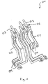
- Figure 1 shows an electrical functional component 01 with a plurality of conductor tracks 02, at the ends of which contact pins 03 are attached in an electrically conductive manner.
- the contact pins 03 are used to attach a Fig. 1 plug, not shown, on functional component 01.
- the conductor tracks 02 are produced by punching out a conductor plate, various connecting webs 04 initially remaining for reasons of assembly.
- the connecting webs 04 are removed after the functional component 01 is encapsulated with plastic, so that all conductor tracks 02 are electrically insulated from one another.
- An electrically conductive contact zone is present between the conductor tracks 02 and the contact pins 03, so that electrical current can be transmitted between the conductor tracks 02 and the contact pins 03 essentially without resistance.
- the electrical contact zone between the conductor tracks 02 and the contact pins 03 is realized by pressing the contact pins 03 into cylindrical recesses at the end of the conductor tracks 02, an annular, cold-pressure-welded transition zone being formed between the conductor tracks 02 and the contact pins 03 by the pressing of the contact pins 03 .
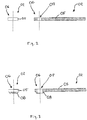
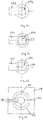
- FIG. 2 The conductor plate 05, from which the conductor tracks 02 are punched out, is first shown in cross section. At the end 06 of the conductor tracks 02, a recess 07 with a cylindrical cross section is made by means of a punching mandrel.
- Figure 3 represents the conductor track 02 after a further manufacturing step.
- the material of the conductor plate 05 is pulled through in the region of the recess 07 by means of a mandrel and the conductor plate 05 is cold-formed in the region of the recess 07 to form a protrusion 08.
- the conductor track 02 thus has a material thickening in the region of the recess 07, the thickness of which is greater than the thickness of the conductor plate 05 used.
- Figure 4 shows the conductor track 02 and the contact pin 03 immediately before being pressed into the recess 07.
- the contact pin 03 is produced by cutting wire sections to length, the cutting to length being carried out by tearing off the contact pins.
- a crack surface is therefore formed on each of the end faces 29, the crack surface in each case bordering on a material constriction 09 which is formed by tearing off the continuous wire.
- the outside diameter of the contact pin 03 is slightly larger, for example by a few tenths of a millimeter, than the inside diameter of the recess 07.
- the constriction 09 allows the contact pin 03 to be inserted and centered in the recess 07 without any problems before being pressed in.
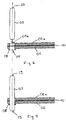
- Figure 5 shows the conductor track 02 and the contact pin 03 after pressing the contact pin 03 into the recess 07; it can be seen that the contact pin 03 projects with both ends beyond the end cross sections of the recess 07. In other words, this means that the contact pin 03 is pushed through the conductor track 02 in order to compensate for dimensional tolerances in the area of the material overlap between the inside diameter of the recess 07 and the outside diameter of the contact pin 03. Since the contact pin 03 is mirror-symmetrical with respect to its center and the two ends have the same shape, the contact pin 03 can be fed in and pressed in with both ends ahead.
- Figure 6 and Figure 7 schematically show a method for through-contacting two conductor tracks 02 and 02a by pressing in a contact pin 03.
- the two conductor tracks 02 and 02a are arranged one above the other in such a way that the two recesses 07 and 07a are aligned with one another.
- By pressing in the contact pin 03 the two ends 09 each projecting beyond the conductor tracks 02 and 02a, the conductor tracks are contacted with one another.
- An insulator layer 10 can be provided between the conductor tracks 02 and 02a.
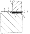
- Figure 8 shows the contact pin 03 and the conductor track 02 in enlarged section A according to Fig. 5 .
- an annular, cold-pressure-welded transition zone 11 is formed, which in Fig. 8 for easier understanding of the invention is only schematized and exemplified on an enlarged scale.
- an annular cold forming zone 12 which consists of the material of the contact pin 03
- an annular welding zone 13 in which the material of the contact pin 03 and the material of the conductor track 02 are integrally welded
- an annular cold forming zone 14 made of the material of the conductor track 02 arranged one behind the other.
- the cold forming zones 12 and 14 and the welding zone 13 arise when the contact pin 03 is pressed into the recess 07 of the conductor track 02 due to the material coverage between the outer circumference 15 of the contact pin 03 and the inner circumference 16 of the recess 07.
- the material coverage is dependent on the choice of material for the To select contact pin 03 and the conductor track 02 so that after pressing the contact pin 03 into the recess 07, a welding zone 13 is formed at least in some areas, in which the contact pin 03 is cold-welded to the conductor track 02. This can be easily checked by making micrographs.
- Fig. 8 illustrated geometry of the cold forming zones 12 and 14 and the welding zone 13 is only to be understood schematically, since the actual Ratios depend very much on the materials used.
- Figure 9 shows the end 06 of the conductor track 02 with the cylindrical recess 07 and the projection 08 in an enlarged cross section.
- Figure 10 shows the end 06 on the track 02 in a view from above. It can be seen that the material of the conductor track 02 encloses the recess 07 in a ring-shaped contact area 17.
- this ring-section-shaped contact area on the inner circumference 16 is not only plastically deformed, but also elastically expanded in the radial direction.
- This elastic expansion causes an elastic restoring force, by means of which the inner circumference 16 is pressed and prestressed against the outer circumference 15 after the contact pin 03 has been pressed in.
- This elastic prestressing of the ring-section-shaped contact region 17 allows creep and aging processes to be compensated for with regard to the electrical line quality, since the material of the conductor track 02 is pressed permanently against the material of the contact pin 03 by the elastic prestressing.
- Figure 11 shows an embodiment 02b of a conductor track.
- a recess 07b with a conical section which in turn also has a projection 08b reaches through.
- the opening angle of the conical recess 07b is in Fig. 11 exaggerated. In most cases, an opening angle of just a few degrees is sufficient to ensure the necessary tolerance compensation.
- Figure 12 shows the conductor track 02b in a view from above, the cross-sectional constriction of the recess 07b with the different diameters being recognized at the two end cross sections.
- Figure 13 shows a further example 02c of a conductor track, at the ends 06c of which a recess 07c is again made.
- the recess 07c also extends through the projection 08c.
- a conical chamfer 19 is attached to the upper end cross-section 18 of the recess 07c in order to facilitate the insertion and centering of the contact pin 03 before the pressing-in.
- Figure 14 shows the conductor track 02c with the chamfer 19 in a view from above.
- Figure 15 shows a further example 02d of a conductor track, on the cylindrical recesses 07d of which a radius 20 is attached in the area of the end cross section 18d, which in turn facilitates the insertion and centering of the contact pin 03 before the pressing.
- Figure 16 shows the conductor track 02d with the radius 20 in a view from above.
- Figure 17 shows a further example 02e of a conductor track with a cylindrical recess 07e, which has chamfers 19 at the end cross sections 21 and 22, respectively.
- the contact pin 03 can be pressed into the recess 07e either from below or from above.
- Figure 18 shows the conductor track 02e in a view from above.
- Figure 19 and Figure 20 show a further example 02f of a conductor track, the cylindrical recess 07f of which has radii 20 at the end cross sections 21 and 22, so that the contact pin 03 can be pressed into the conductor track either from above or from below.
- Figure 21 shows another example 02g of a conductor track with a prismatic recess 07g.
- the prismatic recess 07g has an essentially square cross section, the corners of which are rounded.
- the contact pin to be used in this case, which is pressed into the conductor track 02g, has a complementary shape in cross-section, again providing a suitable material covering in order to form the cold-press-welded transition zone when pressed in.
- Figure 22 and Figure 23 show examples 02h and 02i, which in turn have prismatic recesses 07h and 07i. Either a square chamfer 23 or a square radius 24 is attached to the end cross sections of the recesses 07h and 07i.
- Figure 24 shows a conductor track 25, the rectangular outer circumference of the conductor track 25 being understood only as an example.
- a recess 26 is provided in the conductor track 25, into which a contact pin 03 can be inserted.
- two relief slots 27 are additionally provided in the conductor track 25, which grip around the contact area 28 in sections.
- the relief slots 27 enable an elastic expansion of the annular contact area 28 in the area of the relief slots 27, so that the contact area 28 is elastically pre-tensioned after the contact pin 03 has been pressed in and elastically presses the inner circumference of the recess 26 against the outer circumference of the contact pin 03.
Description
Die Erfindung betrifft ein elektrisches Funktionsbauteil mit zumindest einer Leiterbahn, an der ein Kontaktstift elektrisch leitend angebracht ist, nach dem Oberbegriff des Anspruchs 1. Weiter betrifft die Erfindung ein Verfahren zur Herstellung eines elektrischen Funktionsbauteils.The invention relates to an electrical functional component with at least one conductor track, to which a contact pin is attached in an electrically conductive manner, according to the preamble of claim 1. The invention further relates to a method for producing an electrical functional component.
Gattungsgemäße elektrische Funktionsbauteile sind dadurch charakterisiert, dass am Funktionsbauteil zumindest eine elektrische leitende Leiterbahn vorgesehen ist. An dieser Leiterbahn ist dabei zumindest ein Kontaktstift angebracht. Der Kontaktstift hat dabei die Aufgabe, die Leiterbahn des Funktionsbauteils bevorzugt in lösbarer Weise mit einem funktionskomplementär ausgebildeten Kontaktelement zu kontaktieren. Bei dem funktionskomplementären Kontaktelement kann es sich beispielsweise um Steckelemente in einem Stecker oder einer Fassung handeln. In diesen Fällen ist das elektrische Funktionsbauteil selbst beispielsweise in der Art eines Steckers oder Leuchtmittels ausgebildet. Auch sind gattungsgemäße elektrische Funktionsbauteile bekannt, die in der Art von Leiterplatten ausgebildet sind. An diesen Leiterplatten dienen die Kontaktstifte der Kontaktierung der Leiterplatte, beispielsweise an Steckern oder Steckerleisten.Generic electrical functional components are characterized in that at least one electrically conductive conductor track is provided on the functional component. At least one contact pin is attached to this conductor track. The contact pin has the task of contacting the conductor track of the functional component preferably in a detachable manner with a functionally complementary contact element. The functionally complementary contact element can be, for example, plug elements in a plug or a socket. In these cases, the electrical functional component itself is designed, for example, in the manner of a plug or illuminant. Generic electrical functional components are also known which are designed in the manner of printed circuit boards. Serve on these circuit boards the contact pins of the contacting of the circuit board, for example on plugs or power strips.
Um die elektrische Funktion des Funktionsbauteils zu gewährleisten, ist es gattungsgemäß erforderlich, dass zwischen Leiterbahn und Kontaktstift eine Kontaktzone vorgesehen ist, die die Leiterbahn und den Kontaktstift elektrisch leitend miteinander verbindet. Aufgrund der unterschiedlichen Funktionen von Kontaktstift und Leiterbahn ist es also mit anderen Worten erforderlich, dass diese beiden Bauteile getrennt voneinander gefertigt werden und anschließend in einem Fügeprozess elektrisch leitend und mechanisch belastbar miteinander verbunden werden. Da jede Kontaktstelle einen zusätzlichen elektrischen Widerstand erzeugt, der maßgeblich durch die Einschnürung der stromführenden Flächen in den Mikrokontakten verursacht ist, ist ein sehr guter elektrischer Kontakt zwischen den Kontaktstiften und Leiterbahnen unbedingt erforderlich, um Verlustleistungen zu vermeiden. Außerdem stellt die Kontaktzone zwischen Leiterbahn und Kontaktstift eine potenzielle Fehlerquelle für die Funktion des Funktionsbauteils dar, wenn die Kontaktqualität der Kontaktzone ein bestimmtes Maß unterschreitet.In order to ensure the electrical function of the functional component, it is generally required that a contact zone is provided between the conductor track and the contact pin, which connects the conductor track and the contact pin in an electrically conductive manner. In other words, due to the different functions of the contact pin and the conductor track, it is necessary that these two components are manufactured separately from one another and then connected to one another in an electrically conductive and mechanically load-bearing manner in a joining process. Since each contact point creates an additional electrical resistance, which is largely caused by the constriction of the current-carrying surfaces in the micro-contacts, very good electrical contact between the contact pins and conductor tracks is absolutely necessary in order to avoid power losses. In addition, the contact zone between the conductor track and the contact pin represents a potential source of error for the function of the functional component if the contact quality of the contact zone falls below a certain level.
Neben der Kontaktart ist die wahre metallische Kontaktfläche für die Kontaktqualität von maßgeblicher Bedeutung. Hierbei muss zwischen der Flächenüberdeckung, das heißt der scheinbaren Kontaktfläche zwischen Leiterbahn und Kontaktstift einerseits, und der tatsächlich stromtragenden, wahren metallischen Kontaktfläche unterschieden werden, denn die tatsächlich elektrisch tragende, wahre Kontaktfläche ist bei gleichen geometrischen Verhältnissen wesentlich kleiner. Dies liegt daran, dass auch scheinbar ebene Metalloberflächen sich aufgrund ihrer Oberflächentopographie beziehungsweise Rauheit nicht vollflächig berühren, sondern nur in verhältnismäßig kleinen Bereichen. Je weiter die beiden Kontaktflächen gegeneinander gedrückt werden, umso stärker nähert sich die wahre, elektrisch tragende Kontaktfläche dem Maß der scheinbaren Kontaktfläche an, was durch entsprechende Verformungen der Oberflächenspitzen erreicht wird.In addition to the type of contact, the true metallic contact surface is of crucial importance for the contact quality. A distinction must be made here between the surface coverage, i.e. the apparent contact area between the conductor track and the contact pin, and the actually current-carrying, true metallic contact area, because the true electrical contact area, which is actually electrically carrying, is considerably smaller given the same geometric conditions. This is because even seemingly flat metal surfaces do not touch the entire surface due to their surface topography or roughness, but only in relatively small areas. The further the two contact surfaces are pressed against one another, the closer the true, electrically bearing contact surface approaches the dimension of the apparent contact surface on what is achieved by appropriate deformations of the surface tips.
Insbesondere in der Elektroenergietechnik ist es außerdem bekannt, dass Kontaktflächen über die Zeit altern und dabei der elektrische Widerstand über die Zeit zunimmt. Durch die altersbedingte Widerstandserhöhung können die Kontaktzonen sogar gänzlich zerstört werden. Dieser Mechanismus wird durch unterschiedliche, zeitgleich in den Kontaktzonen ablaufende Alterungsmechanismen (chemische Reaktionen, Elektromigration, Interdiffusion, Reibverschleiß und Kraftabbau) beeinflusst. Abhängig vom Belastungsstrom und den Umgebungsbedingungen kann einer oder können mehrere dieser Mechanismen die Alterung der Kontaktzone beschleunigen. Insbesondere bei thermisch hoch beanspruchten elektrischen Kontakten können aufgrund hoher Betriebstemperaturen der Kraftabbau und die chemischen Reaktionen durch Oxidation und Relaxation die Alterung entscheiden beschleunigen. Die Andruckkraft zwischen den Kontaktflächen kann aufgrund von dynamischen Erholungsprozessen, Kriechen oder Änderungen der mechanischen Eigenschaften des Leitermaterials innerhalb weniger Wochen stark abnehmen. Damit kann sich der Kontaktwiderstand bei geringen Verbindungskräften bezogen auf die Anfangswerte nach der Montage der Verbindung stark erhöhen und dadurch trotz Prüfung der Bauteile Funktionsfehler verursachen.In electrical energy technology in particular, it is also known that contact surfaces age over time and the electrical resistance increases over time. Due to the age-related increase in resistance, the contact zones can even be completely destroyed. This mechanism is influenced by different aging mechanisms (chemical reactions, electromigration, interdiffusion, friction wear and force reduction) that take place simultaneously in the contact zones. Depending on the load current and the environmental conditions, one or more of these mechanisms can accelerate the aging of the contact zone. Particularly in the case of electrical contacts that are subject to high thermal stress, the degradation of force and the chemical reactions through oxidation and relaxation can decisively accelerate aging due to high operating temperatures. The pressure force between the contact surfaces can decrease sharply within a few weeks due to dynamic recovery processes, creeping or changes in the mechanical properties of the conductor material. This means that the contact resistance can increase significantly with low connection forces, based on the initial values after the connection has been installed, and thus cause malfunctions in spite of checking the components.
Zur Herstellung der Kontaktzone zwischen Leiterbahn und Kontaktstift sind aus dem Stand der Technik verschiedene Fügetechniken bekannt, die zugleich für einen ausreichenden elektrischen Kontakt zwischen Leiterbahn und Kontaktstift sorgen und die mechanische Befestigung des Kontaktstifts an der Leiterbahn realisieren. Die am häufigsten eingesetzten Verbindungstechniken zur Herstellung einer Kontaktzone zwischen Leiterbahn und Kontaktstift stellen das Schrauben, das Schweißen und das Nieten dar. Weniger häufig wird auch eine Lötverbindung eingesetzt.Various joining techniques are known from the prior art for producing the contact zone between the conductor track and the contact pin, which at the same time ensure sufficient electrical contact between the conductor track and the contact pin and realize the mechanical attachment of the contact pin to the conductor track. The most commonly used connection techniques for establishing a contact zone between the conductor track and the contact pin are screwing, welding and riveting. Less frequently, a soldered connection is also used.
Bei einer Schraubverbindung erfolgt der Stromschluss nur sekundär und in relativ kleinem Maß über das verwendete schraubbare Verbindungselement. Primär erfolgt der Stromschluss dagegen über die durch die Schraubverbindung erzeugten Kontaktflächen, in denen das Material der Leiterbahn und das Material des Kontaktstifts durch Andruck des Schraubelements gegeneinander gedrückt werden. Für die Kontaktqualität spielen hierbei insbesondere die Rauheit der Bauteiloberflächen und die vorhandenen Oxidationsschichten an den Kontaktflächen eine Rolle. Die Kontaktqualität solcher Schraubverbindungen an gattungsgemäßen elektrischen Funktionsbauteilen ist deshalb relativ gering und weist eine hohe Streuung auf. Nachteilig an derartigen Schraubverbindungen ist es außerdem, dass relativ viele Einzelteile vorgesehen werden müssen, deren Montage aufwendig ist. Bei zyklischen mechanischen Belastungen ist außerdem ein nachträgliches Serviceintervall notwenig, um den notwendigen Andruck zwischen den Kontaktflächen zuverlässig aufrechtzuerhalten.In the case of a screw connection, the electrical connection is only secondary and to a relatively small extent via the screwable connecting element used. In contrast, the electrical connection occurs primarily via the contact surfaces generated by the screw connection, in which the material of the conductor track and the material of the contact pin are pressed against one another by pressing the screw element. The roughness of the component surfaces and the existing oxidation layers on the contact surfaces play a role in the contact quality. The contact quality of such screw connections on generic electrical functional components is therefore relatively low and has a high degree of scatter. It is also a disadvantage of such screw connections that a relatively large number of individual parts must be provided, the assembly of which is complex. In the case of cyclic mechanical loads, a subsequent service interval is also necessary to reliably maintain the necessary pressure between the contact surfaces.
Bei Einsatz von Schweißverfahren zur Kontaktierung zwischen Leiterbahn und Kontaktstift wird aufgrund des Stoffschlusses ein sehr geringer Verbindungswiderstand erreicht. Allerdings ist das Einsatzspektrum solcher Schweißverfahren zum Fügen des Kontaktstifts an der Leiterbahn relativ gering, da beschichtete und thermisch empfindliche Bauteile nicht oder nur sehr schwer geschweißt werden können. Insbesondere beim Fügen von thermisch empfindlichen Bauteilen, beispielsweise elektronischen Bauteilen, oder bei Baugruppen mit vormontierten Kunststoffteilen ist der Wärmeeintrag durch das Schweißen von entscheidendem Nachteil. Auch können Oberflächenbeschichtungen durch die Schweißung nachteilig beeinflusst werden. Weiterhin können auch die Bauteilauslegung und die daraus resultierende Bauteilgeometrie den Einsatz von Schweißen als Fügetechnik verhindern. Bei filigranen Bauteilen, beispielsweise sehr feinen Leiterbahnen, wird durch den Wärmeeintrag des Schweißens außerdem ein Wärmeverzug verursacht, der vielfach auch durch nachträgliches Richten der Bauteile nicht mehr korrigiert werden kann.When using welding processes to make contact between the conductor track and the contact pin, a very low connection resistance is achieved due to the material connection. However, the range of applications for such welding methods for joining the contact pin to the conductor track is relatively small, since coated and thermally sensitive components cannot be welded, or only with great difficulty. In particular when joining thermally sensitive components, for example electronic components, or in assemblies with preassembled plastic parts, the heat input from welding is a decisive disadvantage. Surface coatings can also be adversely affected by the welding. Furthermore, the component design and the resulting component geometry can prevent the use of welding as a joining technique. In the case of filigree components, for example very fine conductor tracks, the heat input from welding also causes heat distortion, which in many cases can no longer be corrected by subsequently straightening the components.
Bei der Verwendung von Nietverfahren zur Kontaktierung des Kontaktstifts mit der Leiterbahn können beispielsweise Kontaktstifte eingesetzt werden, an deren Schaft eine Kontaktniete angeformt ist. Diese Kontaktniete weist dabei einen Bund zur Abstützung im Randbereich einer Ausnehmung in der Leiterbahn auf. Außerdem ist die Kontaktniete mit einem Nietkopf ausgestattet, der auf der gegenüberliegenden Seite der Ausnehmung in der Leiterbahn umgelegt wird und dadurch einen Kraftschluss zwischen Kontaktstift und Leiterbahn realisiert. Dieser Kontaktschluss bewirkt eine axial gerichtete Andruckkraft zwischen der Stirnfläche des Bundes und der inneren Stirnfläche des Nietkopfes einerseits und den gegenüberliegenden Oberflächenbereichen der Leiterbahn andererseits. Eine radial wirkende Andruckkraft an der zylinderförmigen Umfangsfläche der Kontaktniete ist dagegen nicht oder nur in sehr geringem Maße vorhanden. Da keine radial wirkenden Kontaktkräfte in signifikantem Maße erzeugt werden können, ist die Kontaktqualität bei solchen Nietverbindungen relativ gering. Außerdem ist die Herstellung solcher Kontaktnieten am Kontaktstift aufwendig, da der Kontaktschaft, der Bund und der Nietkopfschaft regelmäßig nur durch spanende Fertigungsverfahren, insbesondere durch Drehen von Teilen, hergestellt werden können. Ein signifikanter Nachteil von Nietverbindungen ist ihre hohe Temperaturempfindlichkeit, da sich Nietverbindungen ab einer Umgebungstemperatur von circa 150 °C aufgrund der Materialrelaxation und dem damit verbundenen Kraftabbau lockern und die elektrische Kontaktqualität damit stark abfällt. Auch wird durch die Lockerung der Nietverbindung eine Spaltkorrosion begünstigt, was wiederum zum Ausfall des elektrischen Funktionsbauteils führen kann.When using riveting methods for contacting the contact pin with the conductor track, contact pins can be used, for example, on the shaft of which a contact rivet is formed. This contact rivet has a collar for support in the edge region of a recess in the conductor track. In addition, the contact rivet is equipped with a rivet head which is folded over on the opposite side of the recess in the conductor track and thereby realizes a frictional connection between the contact pin and the conductor track. This contact closure causes an axially directed pressing force between the end face of the collar and the inner end face of the rivet head on the one hand and the opposite surface areas of the conductor track on the other hand. In contrast, a radially acting pressure force on the cylindrical circumferential surface of the contact rivet is nonexistent or only to a very small extent. Since no radially acting contact forces can be generated to a significant degree, the contact quality with such riveted connections is relatively low. In addition, the production of such contact rivets on the contact pin is complex, since the contact shaft, the collar and the rivet head shaft can only be produced regularly by machining production processes, in particular by turning parts. A significant disadvantage of riveted joints is their high temperature sensitivity, since riveted joints loosen from an ambient temperature of around 150 ° C due to the material relaxation and the associated loss of force, and the electrical contact quality drops sharply. The loosening of the rivet connection also favors crevice corrosion, which in turn can lead to the failure of the electrical functional component.
Zur Herstellung des elektrischen Kontakts zwischen Kontaktstift und Leiterbahn können diese auch miteinander verlötet werden. Solche Lötverfahren haben aber den Nachteil, dass eine relativ aufwendige Bearbeitung notwendig ist. Außerdem führt die Zuführung des Lotwerkstoffes häufig zu chemischen Reaktionen der Kontaktpartner, die die Kontaktstelle altern lassen.To establish the electrical contact between the contact pin and the conductor track, these can also be soldered to one another. However, such soldering methods have the disadvantage that relatively complex processing is necessary. In addition, the supply of the solder material often leads to chemical reactions of the contact partners, which cause the contact point to age.
Die
Ausgehend von diesem Stand der Technik ist es Aufgabe der vorliegenden Erfindung, ein neues elektrisches Funktionsbauteil mit einer Kontaktzone zwischen einer Leiterbahn und einem Kontaktstift vorzuschlagen, mit dem die oben beschriebenen Nachteile der gattungsgemäßen Funktionsbauteile vermieden werden. Außerdem ist es Aufgabe der vorliegenden Erfindung, ein neues Verfahren zur Herstellung solcher Funktionsbauteile vorzuschlagen.Starting from this prior art, it is an object of the present invention to propose a new electrical functional component with a contact zone between a conductor track and a contact pin, with which the disadvantages of the generic functional components described above are avoided. In addition, it is an object of the present invention to propose a new method for producing such functional components.
Diese Aufgaben werden durch ein Funktionsbauteil beziehungsweise ein Verfahren nach der Lehre der beiden unabhängigen Hauptansprüche gelöst. Vorteilhafte Ausführungsformen der Erfindung sind Gegenstand der Unteransprüche.These tasks are solved by a functional component or a method according to the teaching of the two independent main claims. Advantageous embodiments of the invention are the subject of the dependent claims.
Das erfindungsgemäße Funktionsbauteil, wobei die elektrisch leitende Kontaktzone zwischen Leiterbahn und Kontaktstift in der Art einer ringförmigen, kaltpressgeschweißten Übergangszone ausgebildet ist, ist dadurch charakterisiert, dass die den Kontaktstift aufnehmende Ausnehmung einen konusabschnittsförmigen Querschnitt aufweist, wobei sich die Ausnehmung in Fügerichtung des Kontaktstifts verengt. Durch Einsatz eines geeigneten Fertigungsverfahrens, insbesondere des nachfolgend noch zu beschreibenden erfindungsgemäßen Verfahrens, werden/wird beim Fügen des Kontaktstifts an der Leiterbahn das Oberflächenmaterial der Leiterbahn und/oder das Oberflächenmaterial des Kontaktstifts in der Übergangszone kalt umgeformt, sodass sich dort in den Randschichten des Materials der Leiterbahn beziehungsweise des Materials des Kontaktstifts eine Kaltumformzone ausbildet. Der Fügedruck ist dabei so hoch zu wählen, dass an oder in zumindest einer Kaltumformzone zumindest eine kaltgeschweißte Schweißzone entsteht, in der der Kontaktstift und die Leiterbahn elektrisch leitend stoffschlüssig miteinander verbunden sind. Da die Kontaktzone ringförmig ausgebildet ist, kann die Ausbildung der Kaltumformzone und der Schweißzone in einfacher Weise dadurch erreicht werden, dass der Außenumfang des Kontaktstifts und der Innenumfang der Ausnehmung beziehungsweise Vertiefung eine materialmäßige Überdeckung aufweist. Diese Überdeckung sorgt beim Einpressen des Kontaktstifts in die Ausnehmung beziehungsweise Vertiefung dafür, dass die beiden Bauteile in ihren oberflächlichen Materialschichten mit hohem Druck gegeneinander gedrückt und aneinander vorbei bewegt werden. Die dabei auftretenden Verformungen im Kristallgitter der beteiligten Fügepartner sorgen für eine zumindest bereichsweise vorhandene stoffschlüssige Verbindung.The functional component according to the invention, the electrically conductive contact zone between the conductor track and the contact pin being designed in the manner of an annular, cold-pressure-welded transition zone, is characterized in that the recess receiving the contact pin has a conical section-shaped cross section, the recess narrowing in the joining direction of the contact pin. By using a suitable production method, in particular the method according to the invention to be described below, the surface material of the conductor path and / or the surface material of the contact pin are / are cold-formed in the transition zone when the contact pin is joined to the conductor track, so that there is in the peripheral layers of the material the conductor track or the material of the contact pin forms a cold forming zone. The joining pressure is to be selected so high that at least one cold-welded welding zone is created on or in at least one cold-forming zone, in which the contact pin and the conductor track are connected to one another in an electrically conductive manner. Since the contact zone is annular, the formation of the cold forming zone and the welding zone can be achieved in a simple manner in that the outer circumference of the contact pin and the inner circumference of the recess or recess have a material overlap. When the contact pin is pressed into the recess or depression, this overlap ensures that the two components in their superficial material layers are pressed against one another with high pressure and moved past one another. The deformations that occur in the crystal lattice of the joining partners involved ensure a cohesive connection, at least in some areas.
Der Toleranzausgleich wird im Hinblick auf die Materialüberdeckung zwischen Kontaktstift und Leiterbahn dadurch vereinfacht, dass der Kontaktstift an zumindest einem Ende eine Querschnittsverengung, nämlich eine konusabschnittsförmigen Querschnitt, aufweist. Durch den enger werdenden Querschnitt des Kontaktstifts in Einpressrichtung kann der Kontaktstift außerdem sehr leicht in der Ausnehmung beziehungsweise der Vertiefung angelegt und zentriert werden. Mit zunehmender Einpresstiefe ergibt sich eine so hohe Materialüberdeckung, dass dann durch entsprechende Kaltumformungen der erfindungsgemäße Effekt der Bildung einer kaltpressgeschweißten Übergangszone ausgebildet wird.The tolerance compensation is simplified with regard to the material coverage between the contact pin and the conductor track in that the contact pin has a cross-sectional constriction, namely a conical section-shaped cross section, at at least one end. Due to the narrowing cross section of the contact pin in the press-in direction, the contact pin can also be very easily placed and centered in the recess or depression. With increasing press-in depth, the material coverage is so high that the effect according to the invention of forming a cold-press-welded transition zone is then formed by appropriate cold forming.
Ob an beiden Fügepartnern jeweils Kaltumformzonen vorhanden sind und wie groß diese beiden Kaltumformzonen relativ zueinander ausfallen, ist insbesondere abhängig vom Kaltumformwiderstand der entsprechenden Materialien beziehungsweise Oberflächenbeschichtungen. Um eine hohe Kontaktqualität zu erreichen, ist es dabei anzustreben, dass beide Fügepartner in ihren oberflächlichen Materialschichten eine Kaltumformzone aufweisen, wobei diese Kaltumformzonen die dazwischen angeordnete Schweißzone schichtförmig umschließen.Whether there are cold forming zones on both joining partners and how large these two cold forming zones are relative to one another depends in particular on the cold forming resistance of the corresponding materials or surface coatings. In order to achieve a high contact quality, it is desirable that both joining partners have a cold-forming zone in their superficial material layers, these cold-forming zones enclosing the welding zone arranged in between in a layered manner.
Das notwendige Maß der Materialüberdeckung zwischen den beiden Fügepartnern kann durch einfache Versuche unter Anfertigung von Schliffbildern der Kontaktzone bestimmt werden. Die Materialüberdeckung darf dabei nur so groß sein, dass eine makroskopische Verformung der beiden Fügepartner durch den Fügeprozess ausgeschlossen ist. Umgekehrt muss die Materialüberdeckung so groß sein, dass sich durch das Einpressen des Kontaktstifts in die Ausnehmung beziehungsweise Vertiefung zumindest bereichsweise eine kaltgeschweißte Schweißzone mit stoffschlüssiger Verbindung zwischen den beiden Fügepartnern ausbildet. Durch Prüfung der Einpresskraft in der laufenden Fertigung bzw. Anfertigung von Schliffbildern und Prüfung der Auszugskraft in Form von Stichprobenprüfung kann dies in einfacher Weise kontrolliert werden.The necessary degree of material coverage between the two joining partners can be determined by simple tests using micrographs of the contact zone. The material coverage may only be so large that a macroscopic deformation of the two joining partners by the joining process is excluded. Conversely, the material coverage must be so large that a cold-welded welding zone with a cohesive connection between the two joining partners is formed, at least in regions, by pressing the contact pin into the recess or recess. This can be checked in a simple manner by checking the press-in force in the ongoing production or preparation of micrographs and testing the pull-out force in the form of random testing.
Das erfindungsgemäße Funktionsbauteil hat gegenüber dem vorbekannten Stand der Technik den Vorteil, dass eine mechanisch hoch belastbare Verbindung zwischen den beiden Fügepartnern einerseits und eine elektrische Kontaktzone mit hoher elektrischer Leitungsqualität in einem Schritt hergestellt werden können. Ein makroskopischer Wärmeeintrag in das Material tritt dabei nicht auf, sodass unerwünschte Verzugseffekte ausgeschlossen sind. Außerdem können Fügepartner mit fast beliebigen Materialeigenschaften mechanisch und elektrisch leitend gleichzeitig miteinander gefügt werden. Die kaltgeschweißte Kontaktzone unterliegt dabei keiner Spaltkorrosion und ein Abfall der Leitungsqualität in der Kontaktzone auch über einen längeren Zeitraum ist nahezu ausgeschlossen.The functional component according to the invention has the advantage over the known prior art that a mechanically highly resilient connection between the two joining partners on the one hand and an electrical contact zone with high electrical line quality can be produced in one step. A macroscopic heat input into the material does not occur, so that undesirable distortion effects are excluded. In addition, joining partners with almost any material properties can be joined together mechanically and electrically. The cold-welded contact zone is not subject to crevice corrosion and a drop in line quality in the contact zone over a longer period of time is almost impossible.
In welcher konstruktiven Weise die Leiterbahn ausgebildet ist, ist grundsätzlich beliebig, solange die Leiterbahn eine ausreichende mechanische Stabilität aufweist, um den Kontaktstift in die Ausnehmung beziehungsweise die Vertiefung einzupressen. Beispielsweise kann es sich bei der Leiterbahn auch um ein massives metallisches Bauteil handeln, wie es beispielsweise zur Herstellung von Steckkontakten an Leuchtmitteln bekannt ist. Im Hinblick auf die Vermeidung eines hohen Wäremeeintrages und der dadurch verursachten unerwünschten Verzugseffekte weist die Erfindung besonders große Vorteile auf, wenn die Leiterbahn in der Art eines Leiterblechs, insbesondere in der Art eines Stanzgitters, ausgebildet ist. An solchen Leiterblechen können hochfiligrane Leiterbahnen vorgesehen sein, die insbesondere durch Ausstanzen preisgünstig herstellbar sind. Durch geeignete Presswerkzeuge mit einer Vielzahl von Aufnahmen für die Kontaktstifte ist es möglich, ein solches Leiterblech in einfacher und kostengünstiger Weise gleichzeitig mit einer Vielzahl von Kontaktstiften auszustatten. Die Kaltumformung unter Bildung der Kaltschweißzone führt dabei außerdem dazu, dass die Kontaktstifte mechanisch hochfest mit dem Leiterblech verbunden werden und somit hohe maximale Ausziehkräfte erreichen.The design of the conductor track is basically as long as the conductor track has sufficient mechanical stability to press the contact pin into the recess or recess. For example, the conductor track can also be a solid metallic component, as is known, for example, for producing plug contacts on lamps. With a view to avoiding a high heat input and the undesirable distortion effects caused thereby, the invention has particularly great advantages if the conductor track is designed in the manner of a conductor plate, in particular in the manner of a lead frame. Highly filigree conductor tracks can be provided on such conductor plates, which can be produced inexpensively in particular by punching out. By means of suitable pressing tools with a large number of receptacles for the contact pins, it is possible to provide such a printed circuit board with a large number of contact pins in a simple and inexpensive manner at the same time. The cold forming to form the cold welding zone also means that the contact pins are mechanically connected to the printed circuit board with high strength and thus achieve high maximum extraction forces.
Die mechanische Festigkeit der Verbindung zwischen dem Kontaktstift und der Leiterbahn und die elektrische Leitungsqualität zwischen Kontaktstift und Leiterbahn wurden maßgeblich davon beeinflusst, wie groß die ringförmige, kaltpressgeschweißte Übergangszone ist. Der Durchmesser der Übergangszone ist dabei vielfach bauartbedingt vorgegeben, da beispielsweise die Breite von Leiterbahnen in Leiterblechen nicht beliebig vergrößerbar ist. Außerdem ist auch der Durchmesser der Stecckontakte vielfach vorgegeben. Insbesondere bei der Verwendung besonders dünner Leiterbahnen ist es deshalb von Vorteil, wenn im Bereich der Kontaktzone ein ringförmiger Überstand an der Leiterbahn vorgesehen ist, der eine Materialverdickung in der Leiterbahn bildet. Ist die Ausnehmung beziehungsweise Vertiefung im Bereich dieses Überstandes angeordnet, so kann dadurch die Höhe der ringförmigen, kaltpressgeschweißten Übergangszone vergrößert werden. Insbesondere ist auch eine Höhe der Übergangszone möglich, die größer als die Dicke der Leiterbahn selbst ist.The mechanical strength of the connection between the contact pin and the conductor track and the electrical line quality between the contact pin and the conductor track were significantly influenced by the size of the annular, cold-pressure-welded transition zone. The diameter of the transition zone is often predetermined due to the type of construction, since for example the width of conductor tracks in conductor plates cannot be increased arbitrarily. In addition, the diameter of the plug contacts is often specified. Particularly when using particularly thin conductor tracks, it is therefore advantageous if an annular protrusion is provided on the conductor track in the region of the contact zone, which protrudes to form a material thickening in the conductor track. If the recess or depression is arranged in the region of this protrusion, the height of the annular, cold-pressure-welded transition zone can thereby be increased. In particular, a height of the transition zone that is greater than the thickness of the conductor track itself is also possible.
Um beim Einpressen der Kontaktstifte in die Ausnehmung einer Leiterbahn einen sicheren Sitz mit hoher Leitungsqualität erreichen zu können, ohne überhohe Toleranzen im Hinblick auf die Durchmesserüberdeckung einhalten zu müssen, ist es besonders vorteilhaft, wenn der Kontaktstift die Leiterbahn in der Ausnehmung vollständig durchgreift und mit beiden Enden über die Leiterbahn zumindest ein Stück weit übersteht. Durch den beidseitigen Überstand des Kontaktstifts über die Leiterbahn ist es beim Einpressen möglich, dass zum Ausgleich von Toleranzen, insbesondere zum Ausgleich von Durchmessertoleranzen, die Durchstecktiefe des Kontaktstifts variiert wird. Insbesondere kann ein derartiger Toleranzausgleich dadurch vereinfacht werden, dass sich der Kontaktstift in Fügerichtung verjüngt beziehungsweise die Ausnehmung sich in Fügerichtung verengt (dazu siehe die Beschreibung weiter unten). Durch die Aufweitung des Kontaktstifts mit zunehmender Einpresstiefe beziehungsweise durch die Verjüngung der Ausnehmung mit zunehmender Einpresstiefe wird erreicht, dass die Materialüberdeckung mit zunehmender Einstecktiefe immer größer wird.In order to be able to achieve a secure fit with high cable quality when the contact pins are pressed into the recess in a conductor track, without excessive tolerances with regard to the diameter coverage Having to comply with it is particularly advantageous if the contact pin completely engages through the conductor track in the recess and protrudes at least a bit with both ends over the conductor track. Due to the protrusion of the contact pin on both sides of the conductor track, it is possible when pressing in that the insertion depth of the contact pin is varied in order to compensate for tolerances, in particular to compensate for diameter tolerances. In particular, such tolerance compensation can be simplified in that the contact pin tapers in the joining direction or the recess narrows in the joining direction (for this, see the description below). By widening the contact pin with increasing insertion depth or by tapering the recess with increasing insertion depth, it is achieved that the material coverage increases with increasing insertion depth.
Die erfindungsgemäße Kontaktierung durch Einpressen eines Kontaktstifts unter Bildung einer kaltpressgeschweißten Übergangszone ist insbesondere auch dann von Vorteil, wenn zwei Leiterbahnen durchkontaktiert werden sollen. Dazu kann dann in beiden Leiterbahnen jeweils eine Ausnehmung vorgesehen werden. Diese Ausnehmungen werden dann übereinander fluchtend angeordnet und der Kontaktstift unter Bildung jeweils einer kaltpressgeschweißten Übergangszone in jeder Ausnehmung durchgesteckt.The contacting according to the invention by pressing in a contact pin to form a cold-pressure-welded transition zone is also particularly advantageous when two conductor tracks are to be contacted. For this purpose, a recess can then be provided in each of the two conductor tracks. These recesses are then aligned one above the other and the contact pin is inserted in each recess to form a cold-welded transition zone.
Die Querschnittsänderung des Kontaktstifts, die zur Bildung einer erwünschten Querschnittsverengung erforderlich ist, kann selbstverständlich durch beliebige Fertigungsverfahren, beispielsweise durch spanabhebende Fertigung der Kontaktstifte, hergestellt werden. Diese Art der Herstellung ist allerdings relativ kostenaufwendig, da es sich bei den Kontaktstiften um Massenteile handelt. Bevorzugt ist es deshalb, wenn der Kontaktstift an zumindest einer Stirnseite eine Rissfläche aufweist und hinter der Stirnseite zumindest über einen kurzen Abschnitt hinweg eine Einschnürung aufweist. Solche Kontaktstifte können durch Anwendung von Reißverfahren an Endlosdrähten sehr kostengünstig hergestellt werden. Dabei kann der beispielsweise stark erwärmte Draht in der Reißvorrichtung in Richtung seiner Längsausstreckung so weit gezogen werden, dass er sich jeweils in einem definierten Abstand einschnürt und quer zur Einschnürung unter Bildung der Stirnseite des Kontaktstifts abreißt. Derartige Kontaktstifte können sehr kostengünstig hergestellt werden und weisen eine hohe Maßgenauigkeit im Hinblick auf den Außendurchmesser auf.The change in cross-section of the contact pin, which is required to form a desired cross-sectional constriction, can of course be produced by any manufacturing method, for example by machining the contact pins. However, this type of production is relatively expensive because the contact pins are mass parts. It is therefore preferred if the contact pin has a crack surface on at least one end face and has a constriction behind the end face at least over a short section. Such contact pins can be applied of tear processes on continuous wires can be produced very inexpensively. In this case, the wire, which is strongly heated, for example, can be pulled so far in the direction of its longitudinal extension in the tearing device that it constricts at a defined distance and tears off transversely to the constriction, forming the end face of the contact pin. Such contact pins can be produced very inexpensively and have high dimensional accuracy with regard to the outer diameter.
Weiterhin ist es besonders vorteilhaft, wenn der Querschnitt des Kontaktstifts bezüglich seiner Mitte spiegelsymmetrisch ausgebildet ist. Durch die spiegelsymmetrische Gestaltung des Kontaktstifts kann erreicht werden, dass der Kontaktstift wahlweise mit dem einen oder dem anderen Ende in die Ausnehmung beziehungsweise Vertiefung eingepresst werden kann. Bei der Zuführung der Kontaktstifte an die Fügevorrichtung ist es von großem Vorteil, dass die Kontaktstifte während der Zuführung nicht in einer Vorzugsrichtung ausgerichtet werden müssen. Stattdessen können für die Zuführung einfache Rütteltöpfe zum Einsatz kommen, die die Kontaktstifte in ihrer Längsrichtung ausrichten, ohne dass dabei Rücksicht auf eine Vorzugsrichtung des Kontaktstifts genommen werden muss.Furthermore, it is particularly advantageous if the cross section of the contact pin is mirror-symmetrical with respect to its center. The mirror-symmetrical design of the contact pin means that one or the other end of the contact pin can optionally be pressed into the recess or depression. When feeding the contact pins to the joining device, it is of great advantage that the contact pins do not have to be aligned in a preferred direction during the feeding. Instead, simple vibrating pots can be used for the feed, which align the contact pins in their longitudinal direction without having to take into account a preferred direction of the contact pin.
Im Hinblick auf die Langzeitstabilität der kaltpressgeschweißten Übergangszone ist es besonders vorteilhaft, wenn die Kontaktzone, in der der Kontaktstift eingepresst wird, an einem Ende der Leiterbahn angeordnet ist. An diesem Ende der Leiterbahn kann dann ein ringabschnittsförmiger Kontaktbereich vorgesehen werden, der die ringförmige, kaltpressgeschweißte Übergangszone allseitig umgreift. Beim Einpressen des Kontaktstifts in diesen ringabschnittsförmigen Kontaktbereich wird das Material der Leiterbahn dann aufgrund der Materialüberdeckung radial aufgeweitet und dabei nicht nur in der Kontaktzone plastisch umgeformt, sondern insgesamt elastisch aufgeweitet. Die daraus resultierenden elastischen Rückstellkräfte bewirken, dass der ringabschnittsförmige Kontaktabschnitt elastisch nach innen gepresst wird und die kaltpressgeschweißte Übergangszone auch über lange Zeiträume spaltfrei zusammenhält.With regard to the long-term stability of the cold-pressure-welded transition zone, it is particularly advantageous if the contact zone in which the contact pin is pressed in is arranged at one end of the conductor track. At this end of the conductor track, a ring-shaped contact area can then be provided, which encompasses the annular, cold-pressure-welded transition zone on all sides. When the contact pin is pressed into this ring-section-shaped contact area, the material of the conductor track is then radially expanded due to the material overlap and is not only plastically deformed in the contact zone, but is elastically expanded overall. The resulting elastic restoring forces cause the ring section-shaped contact section is elastically pressed inwards and the cold-welded transition zone holds together without gaps even over long periods of time.
Wie bereits erläutert, ist die Einhaltung eines exakt definierten Materialüberstandes zwischen dem Außenumfang des Kontaktstifts und dem Innenumfang der Ausnehmung beziehungsweise Vertiefung für die Ausbildung der erfindungsgemäßen kaltpressgeschweißten Übergangszone von großer Bedeutung. Um den Materialüberstand prozesssicher in hohen Stückzahlen einhalten zu können, ist es deshalb besonders vorteilhaft, wenn der Kontaktstift zumindest bereichsweise einen kalibrierten Außenumfang und/oder die Ausnehmung beziehungsweise die Vertiefung einen zumindest bereichsweise kalibrierten Innenumfang aufweisen/aufweist. Durch die Kalibrierung der Umfänge kann eine hohe Maßhaltigkeit gewährleistet werden, die das Einhalten feiner Toleranzen im Bereich des Materialüberstandes ermöglichen.As already explained, compliance with a precisely defined material protrusion between the outer circumference of the contact pin and the inner circumference of the recess or depression is of great importance for the formation of the cold-pressure-welded transition zone according to the invention. In order to be able to reliably maintain the material protrusion in large quantities in a process-safe manner, it is therefore particularly advantageous if the contact pin has / has a calibrated outer circumference at least in some areas and / or the recess or the recess has / has an at least partially calibrated inner circumference. By calibrating the circumference, a high degree of dimensional accuracy can be guaranteed, which enables the maintenance of fine tolerances in the area of the material overhang.
Soweit die verwendeten Materialien zur Herstellung des Kontaktstifts beziehungsweise der Leiterbahn es nur bedingt zulassen, dass eine kaltpressgeschweißte Übergangszone ausgebildet wird, können die Leiterbahn und/oder der Kontaktstift eine metallische Beschichtung aufweisen. Der Umformwiderstand des Beschichtungsmaterials ist dabei geringer zu wählen als der Umformwiderstand des darunter liegenden beschichteten Materials, um auf diese Weise die Ausbildung einer kaltpressgeschweißten Übergangszone zu vereinfachen, denn Materialien mit geringerem Umformwiderstand, beispielsweise Gold oder Silber, ermöglichen es, mit hoher Fügequalität eine kaltpressgeschweißte Übergangszone auszubilden.Insofar as the materials used to produce the contact pin or the conductor track only permit a cold-press-welded transition zone to be formed to a limited extent, the conductor track and / or the contact pin may have a metallic coating. The resistance to deformation of the coating material should be chosen lower than the resistance to deformation of the underlying coated material, in order to simplify the formation of a cold-pressure-welded transition zone, because materials with lower resistance to deformation, e.g. gold or silver, enable a cold-pressure-welded transition zone with high joining quality to train.
Die Querschnittsform des Kontaktstifts beziehungsweise die Querschnittsform der Ausnehmung beziehungsweise der Vertiefung und daraus resultierend die Querschnittsform der ringförmigen, kaltpressgeschweißten Übergangszone ist grundsätzlich beliebig. In den einfachsten Bauformen ist es vorgesehen, dass kreisrunde Kontaktstifte in kreisrunde Ausnehmungen beziehungsweise Vertiefungen eingepresst werden, sodass sich eine zylinderförmige Übergangszone ausbildet. Alternativ dazu kann der Kontaktstift aber auch jede beliebige prismatische Gestalt aufweisen, beispielsweise quadratisch oder vieleckig sein. Der Querschnitt der Ausnehmung beziehungsweise der Vertiefung sollte dabei einen entsprechenden prismatischen Aufbau aufweisen. Im Ergebnis kann damit dann eine kaltpressgeschweißte Übergangszone mit prismatischer Gestalt hergestellt werden.The cross-sectional shape of the contact pin or the cross-sectional shape of the recess or depression and, as a result, the cross-sectional shape of the annular, cold-pressure-welded transition zone is in principle arbitrary. In the simplest designs, it is provided that circular contact pins are circular Recesses or depressions are pressed in, so that a cylindrical transition zone is formed. Alternatively, the contact pin can also have any prismatic shape, for example square or polygonal. The cross section of the recess or depression should have a corresponding prismatic structure. As a result, a cold press welded transition zone with a prismatic shape can then be produced.
An welcher Art von elektrischem Funktionsbauteil die erfindungsgemäße ringförmige, kaltpressgeschweißte Übergangszone vorgesehen ist, ist grundsätzlich beliebig. Besonders vorteilhaft ist diese Art der Anbringung von Kontaktstiften an Leiterbahnen durch ein kaltumformendes Fügeverfahren bei Leiterplatten, Steckern oder Leuchtmitteln.The type of electrical functional component in which the annular, cold-pressure-welded transition zone according to the invention is provided is fundamentally arbitrary. This type of attachment of contact pins to conductor tracks by means of a cold-forming joining process for circuit boards, plugs or lamps is particularly advantageous.
Zur Herstellung des erfindungsgemäßen Funktionsbauteils kann ein Verfahren mit folgenden Verfahrensschritten eingesetzt werden:
- a) Zunächst wird in einer Leiterbahn eine Ausnehmung mit einem konusabschnittsförmigen Querschnitt hergestellt. Dies kann beispielsweise bei Verwendung einer Leiterplatte aus Blech durch Einsatz eines Stanzwerkzeuges geschehen, mit dem das Leiterblech durchgestanzt wird.
- b) Anschließend wird einer oder werden mehrere Kontaktstifte zugeführt, wobei der Außenumfang des Kontaktstifts zumindest abschnittsweise größer als der Innenumfang der konusabschnittsförmigen Ausnehmung ist. Das eine Ende des Kontaktstifts wird in die konusabschnittsförmige Ausnehmung eingeführt beziehungsweise angelegt.
- c) Befinden sich Kontaktstift und Ausnehmung beziehungsweise Vertiefung in der richtigen Relativlage, wird durch Einsatz eines geeigneten Werkzeuges, beispielsweise eines Pressstempels mit Vertiefungen, in denen die Kontaktstifte gehalten sind, der Kontaktstift in die konusabschnittsförmige Ausnehmung eingepresst. Aufgrund der Materialüberdeckung zwischen Kontaktstift einerseits und der Ausnehmung der Leiterbahn andererseits bildet sich beim Einpressen eine ringförmige, kaltpressgeschweißte Übergangszone. Diese Übergangszone beinhaltet eine Schweißzone, in der Kontaktstift und Leiterbahn elektrisch leitend miteinander verbunden sind.
- a) First, a recess with a conical section-shaped cross section is produced in a conductor track. This can be done, for example, when using a printed circuit board made of sheet metal by using a punching tool with which the printed circuit board is punched through.
- b) Then one or more contact pins are fed in, the outer circumference of the contact pin being at least in sections larger than the inner circumference of the cone-section-shaped recess. One end of the contact pin is inserted or put into the conical section-shaped recess.
- c) If the contact pin and recess or depression are in the correct relative position, the contact pin is pressed into the conical section-shaped recess by using a suitable tool, for example a press ram with depressions in which the contact pins are held. Because of the material coverage Between the contact pin on the one hand and the recess of the conductor track on the other hand, an annular, cold-press-welded transition zone is formed when pressed in. This transition zone contains a welding zone in which the contact pin and the conductor track are connected to one another in an electrically conductive manner.
Zur Herstellung der Ausnehmung in einem Leiterblech kann ein Stanzwerkzeug eingesetzt werden, mit dem das Leiterblech durchgelocht wird.To produce the recess in a printed circuit board, a punching tool can be used to perforate the printed circuit board.
Zur Herstellung eines ringförmigen Überstandes im Bereich der Ausnehmung eines Leiterblechs kann ein Dorn eingesetzt werden, mit dem das Material des Leiterblechs durchgezogen wird. Dadurch kann eine Höhe der Übergangszone erreicht werden, die größer ist als die Dicke des verwendeten Leiterblechs.A mandrel can be used to produce an annular protrusion in the area of the recess of a conductor plate, with which the material of the conductor plate is pulled. As a result, a height of the transition zone can be achieved which is greater than the thickness of the conductor plate used.
Um die Ausnehmung im Leiterblech auf einen eng tolerierten Durchmesser zu kalibrieren, kann ein Kalibrierdorn oder ein sonstiges Kalibrierwerkzeug in die Ausnehmung eingeführt und durchgesteckt werden.In order to calibrate the recess in the printed circuit board to a narrowly tolerated diameter, a calibration mandrel or another calibration tool can be inserted into the recess and pushed through.
Um zwei Leiterbahnen durchzukontaktieren, werden diese mit zueinander fluchtenden Ausnehmungen übereinander angeordnet und dann wird ein Kontaktstift durch beide Ausnehmungen gleichzeitig zumindest teilweise durchgreifend eingepresst.In order to make contact with two conductor tracks, these are arranged one above the other with recesses aligned with one another, and then a contact pin is pressed in at least partially through both recesses simultaneously.
Werden auf diese Weise mehrere Kontaktstifte gleichzeitig durch beide Leiterbahnen durchkontaktiert, so kann dadurch auch eine Befestigung der beiden Leiterbahnen relativ zueinander realisiert werden.If a plurality of contact pins are contacted through both conductor tracks at the same time in this way, the two conductor tracks can also be fastened relative to one another.
Besonders kostengünstig wird das erfindungsgemäße Verfahren, wenn zur Herstellung des Kontaktstifts ein endloses Drahtmaterial in Drahtabschnitte, insbesondere mit endseitigen Einschnürungen, gerissen wird.The method according to the invention becomes particularly cost-effective if an endless wire material is torn into wire sections, in particular with constrictions at the ends, in order to produce the contact pin.
Verschiedene Ausführungsformen der Erfindung sind in den Zeichnungen teilweise schematisch dargestellt und werden nachfolgend beispielhaft erläutert.Various embodiments of the invention are partially shown schematically in the drawings and are explained below by way of example.
Es zeigen:
- Fig. 1
- ein elektrisches Funktionsbauteil mit mehreren Leiterbahnen und Kontaktelementen in perspektivischer Ansicht;
- Fig. 2
- eine Leiterbahn des Funktionsbauteils gemäß
Fig. 1 vor der Anbringung eines Überstandes im Querschnitt und in seitlicher Ansicht; - Fig. 3
- die Leiterbahn gemäß
Fig. 2 nach Anbringen eines Überstandes und vor Anbringen eines Kontaktstifts im Querschnitt und in seitlicher Ansicht; - Fig. 4
- die Leiterbahn gemäß
Fig. 3 bei Anlegen eines Kontaktstifts vor dem Einpressen im Querschnitt und in seitlicher Ansicht; - Fig. 5
- die Leiterbahn mit dem Kontaktstift gemäß
Fig. 4 nach dem Einpressen im Querschnitt und in seitlicher Ansicht; - Fig. 6
- zwei Leiterbahnen beim Anlegen eines gemeinsamen Kontaktstifts vor dem Einpressen im Querschnitt;
- Fig. 7
- die Leiterbahnen mit dem Kontaktstift gemäß
Fig. 6 nach dem Einpressen im Querschnitt; - Fig. 8
- die Kontaktzone zwischen der Leiterbahn und dem Kontaktstift gemäß
Fig. 5 im vergrößerten Ausschnitt A; - Fig. 9
- eine Leiterbahn mit zylindrischer Ausnehmung und Überstand im Querschnitt;
- Fig. 10
- die Leiterbahn gemäß
Fig. 9 in Ansicht von oben; - Fig. 11
- eine zweite Leiterbahn mit konusabschnittsförmiger Ausnehmung im Querschnitt;
- Fig. 12
- die Leiterbahn gemäß
Fig. 11 in Ansicht von oben; - Fig. 13
- eine Leiterbahn mit zylindrischer Ausnehmung und einer Fase an einem der Endquerschnitte im Querschnitt;
- Fig. 14
- die Leiterbahn gemäß
Fig. 13 in Ansicht von oben; - Fig. 15
- eine weitere Leiterbahn mit zylindrischer Ausnehmung und einem Radius an einem Endquerschnitt im Querschnitt;
- Fig. 16
- die Leiterbahn gemäß
Fig. 15 im Querschnitt; - Fig. 17
- eine weitere Leiterbahn mit zylindrischer Ausnehmung und zwei Fasen an beiden Endquerschnitten im Querschnitt;
- Fig. 18
- die Leiterbahn gemäß
Fig. 17 in Ansicht von oben; - Fig. 19
- eine weitere Leiterbahn mit zylindrischer Ausnehmung und zwei Radien an beiden Endquerschnitten im Querschnitt;
- Fig. 20
- die Leiterbahn gemäß
Fig. 19 in Ansicht von oben; - Fig. 21
- eine Leiterbahn mit einer prismatischen, nämlich quadratförmigen, Ausnehmung in Ansicht von oben;
- Fig. 22
- eine Leiterbahn mit einer prismatischen, nämlich rechteckförmigen, Ausnehmung und einer Fase an den Endquerschnitten in Ansicht von oben;
- Fig. 23
- eine Leiterbahn mit prismatischer, nämlich rechteckförmiger, Ausnehmung mit einem Radius an den Endquerschnitten in Ansicht von oben; und
- Fig. 24
- einer quadratischen Leiterbahn mit zylindrischer Ausnehmung und kreisabschnittsförmigen Entlastungsöffnungen in Ansicht von oben.
- Fig. 1
- an electrical functional component with several conductor tracks and contact elements in a perspective view;
- Fig. 2
- a conductor track of the functional component according to
Fig. 1 before attaching a protrusion in cross-section and in a side view; - Fig. 3
- the conductor track according to
Fig. 2 after attaching a protrusion and before attaching a contact pin in cross-section and in a side view; - Fig. 4
- the conductor track according to
Fig. 3 when creating a contact pin before pressing in cross-section and in a side view; - Fig. 5
- the conductor track with the contact pin according to
Fig. 4 after pressing in cross-section and in a side view; - Fig. 6
- two conductor tracks when creating a common contact pin before pressing in cross section;
- Fig. 7
- the conductor tracks with the contact pin according to
Fig. 6 after pressing in cross section; - Fig. 8
- the contact zone between the conductor track and the contact pin according to
Fig. 5 in enlarged section A; - Fig. 9
- a conductor track with a cylindrical recess and protrusion in cross section;
- Fig. 10
- the conductor track according to
Fig. 9 in top view; - Fig. 11
- a second conductor track with a conical section-shaped recess in cross section;
- Fig. 12
- the conductor track according to
Fig. 11 in top view; - Fig. 13
- a conductor track with a cylindrical recess and a chamfer on one of the end cross sections in cross section;
- Fig. 14
- the conductor track according to
Fig. 13 in top view; - Fig. 15
- a further conductor track with a cylindrical recess and a radius at an end cross section in cross section;
- Fig. 16
- the conductor track according to
Fig. 15 in cross section; - Fig. 17
- another conductor track with a cylindrical recess and two chamfers on both end cross sections in cross section;
- Fig. 18
- the conductor track according to
Fig. 17 in top view; - Fig. 19
- another conductor track with a cylindrical recess and two radii at both end cross sections in cross section;
- Fig. 20
- the conductor track according to
Fig. 19 in top view; - Fig. 21
- a conductor track with a prismatic, namely square, recess in a view from above;
- Fig. 22
- a conductor track with a prismatic, namely rectangular, recess and a chamfer on the end cross sections in a view from above;
- Fig. 23
- a conductor track with a prismatic, namely rectangular, recess with a radius at the end cross sections in a view from above; and
- Fig. 24
- a square conductor track with a cylindrical recess and relief openings in the form of a circular section, viewed from above.
Die Leiterbahnen 02 sind durch Ausstanzen eines Leiterblechs hergestellt, wobei aus Montagegründen zunächst noch diverse Verbindungsstege 04 verbleiben. Die Verbindungsstege 04 werden nach dem Umspritzen des Funktionsbauteils 01 mit Kunststoff entfernt, sodass alle Leiterbahnen 02 elektrisch voneinander isoliert sind.The conductor tracks 02 are produced by punching out a conductor plate, various connecting
Zwischen den Leiterbahnen 02 und den Kontaktstiften 03 ist jeweils eine elektrisch leitende Kontaktzone vorhanden, sodass elektrischer Strom zwischen den Leiterbahnen 02 und den Kontaktstiften 03 im Wesentlichen widerstandsfrei übertragen werden kann. Die elektrische Kontaktzone zwischen den Leiterbahnen 02 und den Kontaktstiften 03 wird dabei durch Einpressen der Kontaktstifte 03 in zylindrische Ausnehmungen am Ende der Leiterbahnen 02 realisiert, wobei durch das Einpressen der Kontaktstifte 03 eine ringförmige, kaltpressgeschweißte Übergangszone zwischen den Leiterbahnen 02 und den Kontaktstiften 03 ausgebildet wird. Das Verfahren zur Herstellung der elektrisch leitenden Kontaktzone zwischen den Kontaktstiften 03 und den Leiterbahnen 02 soll nachfolgend anhand der Zeichnungen
In
Durch Kalibrierung des Außenumfangs 15 am Kontaktstift 03 beziehungsweise durch alternative beziehungsweise additive Kalibrierung des Innenumfangs 16 in der Ausnehmung 07 der Leiterbahn 02 kann eine sichere Prozesssteuerung bei der Ausbildung der Schweißzone 13 erreicht werden, die für eine hohe Kontaktqualität zwischen Kontaktstift 03 und Leiterbahn 02 sorgt. Durch Anbringung von Beschichtungen im Bereich des Außenumfangs 15 beziehungsweise des Innenumfangs 16 kann außerdem die Qualität des elektrischen Kontakts in der Schweißzone 13 erhöht werden.By calibrating the
Claims (14)
- An electrical functional component (01) having at least one electrically conductive conductor strip (02b) and at least one contact pin (03), said contact pin (03) being mounted on the conductor strip (02b) and being able to be contacted with a contact element complementary in function, in particular in a plug or a socket, and a contact zone being provided between the conductor strip (02b) and the contact pin (03), said contact zone electrically connecting the conductor strip (02b) and the contact pin (03) to each other, the contact zone being formed by pressing the contact pin (03) into a recess (07b) of the conductor strip (02b) and the electrically conductive contact zone being formed in the type of an annular cold-pressure-welded transition zone (11), the surface material of the conductor strip (02b) and/or the surface material of the contact pin (03) comprising at least one cold-working area (12, 14) in the transition zone (11), a welding zone (13) being provided at least in sections on or in at least one cold-working zone (12, 14), the contact pin (03) and the conductor strip (02b) being connected to each other in the welding zone (13) by material bonding in an electrically conductive manner,
characterised in that
the recess (07b) receiving the contact pin (03) comprises a cone-segment-shaped cross section, the recess (07b) narrowing in the joining direction of the contact pin (03). - The electrical functional component according to claim 1,
characterised in that
the conductor strip (02b) is formed by a conductive sheet (05), in particular a punched grid. - The electrical functional component according to claim 1 or 2,
characterised in that
the conductor strip (02b) comprises an annular protrusion (08b) in the area of the contact zone, said protrusion (08b) forming a material thickening in the conductor strip (02b). - The electrical functional component according to any one of the claims 1 to 3,
characterised in that
the contact pin (03) engages entirely through the conductor strip (02b) in a recess (07b) and at least partially protrudes over the conductor strip (02b) with both ends. - The electrical functional component according to any one of the claims 1 to 4,
characterised in that
the contact pin (03) comprises a cross-sectional reduction on at least one end, in particular a chamfer or a radius on at least one end cross section or a cone-segment-shaped cross section. - The electrical functional component according to claim 5,
characterised in that
the contact pin comprises a tear surface on at least one frontal side (29), the cross section of the contact pin being constricted at the frontal side (29). - The electrical functional component according to any one of the claims 1 to 6,
characterised in that
the contact pin (03) comprises an outer perimeter (15) calibrated at least in sections and/or that the recess (07b) comprises an inner perimeter (16) calibrated at least in sections. - The electrical functional component according to any one of the claims 1 to 7,
characterised in that
the conductor strip (02b) and/or the contact pin (03) comprise(s) a metallic coating. - The electrical functional component according to claim 8,
characterised in that
the resistance to deformation of the coating material is less than the resistance to deformation of the coated material. - The electrical functional component according to any one of the claims 1 to 9,
characterised in that
the functional component (01) is realised in the type of a printed circuit board or a plug or an illuminant. - A method for producing an electrical functional component (01), comprising the following method steps:a) producing at least one recess (07b) having a cone-segment-shaped cross section in an electrically conductive conductor strip (02b);b) supplying a contact pin (03), whose outer perimeter (15) is larger than the inner perimeter (16) of the cone-segment-shaped recess (07b) at least in sections, an end of the contact pin (03) being disposed at or inserted into the cone-segment-shaped recess (07b), the recess (07b) narrowing in the joining direction of the contact pin (03);c) pressing the contact pin (03) into the cone-segment-shaped recess (07b), an annular cold-pressure-welded transition zone (11) being formed by the cross-sectional overlap between the contact pin (03) on the one hand and the recess (07b) in the conductor strip (02b) on the other hand while the contact pin (03) is pressed in, said contact pin (03) and said conductor strip (02b) being electrically connected to each other in the welding zone (13) of the transition zone (11) by material bonding.
- The method according to claim 11,
characterised in that
a conductive sheet (05) is hole-punched in method step a) using a punching tool. - The method according to claim 12,
characterised in that
the hole-punched conductive sheet (05) is pervaded, in particular by means of a mandrel, resulting in the formation of an annular protrusion (08b). - The method according to any one of the claims 11 to 13,
characterised in that
a continuous wire material is torn into wire sections, in particular having constrictions at their ends, in order to produce the contact pin (03), tear surfaces being formed at the frontal sides (29) of the contact pin (03).
Applications Claiming Priority (2)
| Application Number | Priority Date | Filing Date | Title |
|---|---|---|---|
| DE102015100149.7A DE102015100149A1 (en) | 2015-01-08 | 2015-01-08 | Electrical functional component with contact pin and method for producing an electrical functional component |
| PCT/EP2015/079246 WO2016110369A1 (en) | 2015-01-08 | 2015-12-10 | Electrical functional component having a contact pin, and method for producing an electrical functional component |
Publications (2)
| Publication Number | Publication Date |
|---|---|
| EP3243246A1 EP3243246A1 (en) | 2017-11-15 |
| EP3243246B1 true EP3243246B1 (en) | 2020-04-29 |
Family
ID=55027699
Family Applications (1)
| Application Number | Title | Priority Date | Filing Date |
|---|---|---|---|
| EP15817113.2A Active EP3243246B1 (en) | 2015-01-08 | 2015-12-10 | Electrical functional component having a contact pin, and method for producing an electrical functional component |
Country Status (5)
| Country | Link |
|---|---|
| US (1) | US10700445B2 (en) |
| EP (1) | EP3243246B1 (en) |
| CN (1) | CN107112706B (en) |
| DE (1) | DE102015100149A1 (en) |
| WO (1) | WO2016110369A1 (en) |
Families Citing this family (5)
| Publication number | Priority date | Publication date | Assignee | Title |
|---|---|---|---|---|
| DE102015119785B4 (en) * | 2015-11-04 | 2020-03-26 | ept Holding GmbH & Co. KG | Hole contour for press-fit technology in a lead frame |
| DE102017109034B4 (en) | 2017-04-27 | 2021-11-11 | Te Connectivity Germany Gmbh | Plug connection, electrical connector and method for establishing an electrical connection |
| DE102017110696A1 (en) * | 2017-05-17 | 2018-11-22 | Hanon Systems | Busbar and method for contacting an electric motor |
| DE102018218001B4 (en) * | 2018-10-22 | 2021-09-30 | Schott Ag | Method for producing a connection pin for bushings, as well as connection pin |
| DE102019203166A1 (en) * | 2019-03-08 | 2020-09-10 | Zf Friedrichshafen Ag | Connection of a busbar to another live element |
Citations (1)
| Publication number | Priority date | Publication date | Assignee | Title |
|---|---|---|---|---|
| US3718750A (en) | 1971-10-12 | 1973-02-27 | Gen Motors Corp | Electrical connector |
Family Cites Families (18)
| Publication number | Priority date | Publication date | Assignee | Title |
|---|---|---|---|---|
| US3252204A (en) * | 1962-12-19 | 1966-05-24 | Gen Motors Corp | Method of mounting a connector member to a support member |
| US3805214A (en) * | 1972-08-22 | 1974-04-16 | Amp Inc | Resilient electrical contact |
| US5083928A (en) * | 1991-04-25 | 1992-01-28 | E. I. Du Pont De Nemours And Company | Electrical pin tips |
| SE510056C2 (en) * | 1997-08-07 | 1999-04-12 | Ssab Hardtech Ab | Ways to manufacture a hardened steel detail |
| GB2330336A (en) * | 1997-10-14 | 1999-04-21 | Alliedsignal Ltd | Energy absorbing device for a seat belt |
| DE10138458A1 (en) * | 2001-08-04 | 2003-02-27 | Siemens Ag | Electrical circuit with strip-shaped conductors |
| EP1720387A1 (en) * | 2005-05-03 | 2006-11-08 | Franz Broch | High current terminal with press fit portion |
| US8092129B2 (en) * | 2006-04-21 | 2012-01-10 | Hubbell Incorporated | Bonding washer |
| WO2010093971A1 (en) * | 2009-02-13 | 2010-08-19 | Once Innovations, Inc. | Light emitting diode assembly and methods |
| DE102009043176A1 (en) * | 2009-09-26 | 2011-04-21 | Amphenol-Tuchel Electronics Gmbh | Press-in connector for forming electrical and mechanical connecting arrangement between printed circuit board and e.g. metallic bus bar in hybrid drive of vehicle, has retaining section connecting printed circuit board with line element |
| DE102010001418A1 (en) * | 2010-02-01 | 2011-08-04 | Robert Bosch GmbH, 70469 | Sensor module i.e. low pressure sensor module, for examining exhaust gas in exhaust system of combustion engine in motor car, has housing region comprising recess that is filled with sealant i.e. adhesive sealant |
| JP5570383B2 (en) * | 2010-10-15 | 2014-08-13 | 株式会社神戸製鋼所 | Conductive connecting member, method of manufacturing conductive connecting member, and battery having conductive connecting member as electrode |
| KR102115861B1 (en) * | 2011-08-29 | 2020-05-27 | 가부시키가이샤 지에스 유아사 | Connection body, method for manufacturing connection body, power storage element and method for manufacturing power storage element |
| EP2658036B1 (en) * | 2011-10-06 | 2019-06-12 | Tyco Electronics Belgium EC BVBA | Electrical connection assembly |
| DE102011122371A1 (en) * | 2011-12-22 | 2013-06-27 | Kathrein-Werke Kg | Electrical connection device for producing a soldered connection |
| US9021682B2 (en) * | 2011-12-29 | 2015-05-05 | Taiwan Semiconductor Manufacturing Company, Ltd. | Apparatus for stud bump formation |
| DE102013111963A1 (en) | 2012-11-14 | 2014-05-15 | Walter Söhner GmbH & Co. KG | Plate element with deep drawing bore for press-fit contacts |
| DE102014208101A1 (en) | 2014-04-29 | 2015-10-29 | Robert Bosch Gmbh | Electrical connection arrangement for the electrical connection of printed circuit boards with each other by means of solder-free press-fitting |
-
2015
- 2015-01-08 DE DE102015100149.7A patent/DE102015100149A1/en not_active Withdrawn
- 2015-12-10 US US15/541,198 patent/US10700445B2/en active Active
- 2015-12-10 WO PCT/EP2015/079246 patent/WO2016110369A1/en active Application Filing
- 2015-12-10 CN CN201580072348.4A patent/CN107112706B/en active Active
- 2015-12-10 EP EP15817113.2A patent/EP3243246B1/en active Active
Patent Citations (1)
| Publication number | Priority date | Publication date | Assignee | Title |
|---|---|---|---|---|
| US3718750A (en) | 1971-10-12 | 1973-02-27 | Gen Motors Corp | Electrical connector |
Non-Patent Citations (7)
| Title |
|---|
| ANONYMOUS: "CuNi9Sn2 Werkstoff-Datenblätter", DEUTSCHES KUPFERINSTITUT, 2005, pages 1 - 11, XP055779261 |
| ANONYMOUS: "CuZn30 Werkstoff-Datenblätter", DEUTSCHES KUPFERINSTITUT, 2005, pages 1 - 12, XP055779265 |
| ANONYMOUS: "Diaphragm / piston pressure switches hex 27 with integrated connector", SUCO PROSPECT 0132 - 0137, pages 1 - 2 |
| ANONYMOUS: "Membran- / Kolbendruckschalter SW 27 mit integriertem Stecker", SUCO PROSPECT 0132 - 0137, pages 1 - 2 |
| ANONYMOUS: "Präzisionskontaktstifte für elektrische Steckverbinder", ELBIK GMBH, PRESSEMITTEILUNG - PRESSEBOX, 23 April 2006 (2006-04-23), pages 1 - 2, XP055779269, Retrieved from the Internet <URL:https://www.pressebox.de/inaktiv/elbik-gmbh/Praezisionskontaktstifte-fuer-elektrische-Steckverbinder/boxid/84445> |
| ROLAND H. KILGUS: "Metalltechnik Der Werkzeugbau9. neubearbeitete Auflage", 1986, VERLAG EUROPA-LEHRMITTEL, article "1.2 Scherschneiden", pages: 3, 8 - 9, XP055779252 |
| WOLFGANG BRANDT: "Kontaktstifte / thermisch gerissene Kontaktstifte für Stecker, Steckverbinder, Pfostenleisten usw.", 29 November 2013 (2013-11-29), pages 1 - 3, XP055779277, Retrieved from the Internet <URL:http://www.antriebstechnik.eu/kontaktstifte.htm> |
Also Published As
| Publication number | Publication date |
|---|---|
| CN107112706B (en) | 2020-07-10 |
| WO2016110369A1 (en) | 2016-07-14 |
| CN107112706A (en) | 2017-08-29 |
| US20170365936A1 (en) | 2017-12-21 |
| US10700445B2 (en) | 2020-06-30 |
| DE102015100149A1 (en) | 2016-07-14 |
| EP3243246A1 (en) | 2017-11-15 |
Similar Documents
| Publication | Publication Date | Title |
|---|---|---|
| EP3243246B1 (en) | Electrical functional component having a contact pin, and method for producing an electrical functional component | |
| EP3031564B1 (en) | Help element for pressing into a first work piece in a welding process between two workpieces not directly weldable | |
| EP1754285B1 (en) | Press-in contact | |
| EP1997187A1 (en) | Contact pin and method for its production | |
| DE102007014356A1 (en) | Pin for insertion into a receiving opening of a printed circuit board and method for inserting a pin in a receiving opening of a printed circuit board | |
| WO2006005291A1 (en) | Method for connecting at least one wire to a contact element | |
| DE102011122371A1 (en) | Electrical connection device for producing a soldered connection | |
| DE102013209407A1 (en) | Method for solderless electrical press-in contacting of electrically conductive press-fit pins in printed circuit boards | |
| EP2796017B1 (en) | Method for producing an electrical radiofrequency connection between two plate-shaped conductor track sections and an associated electrical radiofrequency connection | |
| EP3378128B1 (en) | Assembly with a contact element and an electrical cable and method for producing such an assembly | |
| DE102014208101A1 (en) | Electrical connection arrangement for the electrical connection of printed circuit boards with each other by means of solder-free press-fitting | |
| EP3022805A1 (en) | Contact device for establishing an electrical connection to a contact point of a printed circuit board | |
| EP2638988B1 (en) | System comprising a self-piercing rivet and workpieces, and method for joining said workpieces using said rivet | |
| DE102013100564B4 (en) | actuator | |
| WO2014076122A1 (en) | Plate element with a deep-drawn hole for press-in contacts | |
| DE102010039204A1 (en) | Electrical contact used for assembling e.g. gear wheel in gear box for vehicle, has flexible foil and insertion pin that are press-fitted into insertion interface which is made of conductive plastic material | |
| WO2015197265A1 (en) | Method for producing a chassis component | |
| EP1003243A2 (en) | Process for manufacturing an electrical connection to a metal sheet and mounting assembly | |
| EP1898496B1 (en) | Metal contact element for an electric contact assembly | |
| DE102019133891A1 (en) | Functional element | |
| EP3800749B1 (en) | Method of manufacturing an electrically conductive contact element, electrically conductive contact element and sleeve with an electrically conductive contact element | |
| DE102021113511B3 (en) | Resistance welding method and device for resistance welding | |
| EP3629420B1 (en) | Press joint | |
| EP3736920B1 (en) | Contact terminal and method of manufacturing same | |
| WO2018162629A1 (en) | Method for connecting a sandwich component |
Legal Events
| Date | Code | Title | Description |
|---|---|---|---|
| STAA | Information on the status of an ep patent application or granted ep patent |
Free format text: STATUS: THE INTERNATIONAL PUBLICATION HAS BEEN MADE |
|
| PUAI | Public reference made under article 153(3) epc to a published international application that has entered the european phase |
Free format text: ORIGINAL CODE: 0009012 |
|
| STAA | Information on the status of an ep patent application or granted ep patent |
Free format text: STATUS: REQUEST FOR EXAMINATION WAS MADE |
|
| 17P | Request for examination filed |
Effective date: 20170707 |
|
| AK | Designated contracting states |
Kind code of ref document: A1 Designated state(s): AL AT BE BG CH CY CZ DE DK EE ES FI FR GB GR HR HU IE IS IT LI LT LU LV MC MK MT NL NO PL PT RO RS SE SI SK SM TR |
|
| AX | Request for extension of the european patent |
Extension state: BA ME |
|
| DAV | Request for validation of the european patent (deleted) | ||
| DAX | Request for extension of the european patent (deleted) | ||
| STAA | Information on the status of an ep patent application or granted ep patent |
Free format text: STATUS: EXAMINATION IS IN PROGRESS |
|
| 17Q | First examination report despatched |
Effective date: 20190614 |
|
| GRAP | Despatch of communication of intention to grant a patent |
Free format text: ORIGINAL CODE: EPIDOSNIGR1 |
|
| STAA | Information on the status of an ep patent application or granted ep patent |
Free format text: STATUS: GRANT OF PATENT IS INTENDED |
|
| INTG | Intention to grant announced |
Effective date: 20191219 |
|
| GRAS | Grant fee paid |
Free format text: ORIGINAL CODE: EPIDOSNIGR3 |
|
| GRAA | (expected) grant |
Free format text: ORIGINAL CODE: 0009210 |
|
| STAA | Information on the status of an ep patent application or granted ep patent |
Free format text: STATUS: THE PATENT HAS BEEN GRANTED |
|
| AK | Designated contracting states |
Kind code of ref document: B1 Designated state(s): AL AT BE BG CH CY CZ DE DK EE ES FI FR GB GR HR HU IE IS IT LI LT LU LV MC MK MT NL NO PL PT RO RS SE SI SK SM TR |
|
| REG | Reference to a national code |
Ref country code: GB Ref legal event code: FG4D Free format text: NOT ENGLISH |
|
| REG | Reference to a national code |
Ref country code: CH Ref legal event code: EP |
|
| REG | Reference to a national code |
Ref country code: AT Ref legal event code: REF Ref document number: 1264710 Country of ref document: AT Kind code of ref document: T Effective date: 20200515 |
|
| REG | Reference to a national code |
Ref country code: DE Ref legal event code: R096 Ref document number: 502015012463 Country of ref document: DE |
|
| REG | Reference to a national code |
Ref country code: IE Ref legal event code: FG4D Free format text: LANGUAGE OF EP DOCUMENT: GERMAN |
|
| REG | Reference to a national code |
Ref country code: NL Ref legal event code: MP Effective date: 20200429 |
|
| REG | Reference to a national code |
Ref country code: LT Ref legal event code: MG4D |
|
| PG25 | Lapsed in a contracting state [announced via postgrant information from national office to epo] |
Ref country code: GR Free format text: LAPSE BECAUSE OF FAILURE TO SUBMIT A TRANSLATION OF THE DESCRIPTION OR TO PAY THE FEE WITHIN THE PRESCRIBED TIME-LIMIT Effective date: 20200730 Ref country code: LT Free format text: LAPSE BECAUSE OF FAILURE TO SUBMIT A TRANSLATION OF THE DESCRIPTION OR TO PAY THE FEE WITHIN THE PRESCRIBED TIME-LIMIT Effective date: 20200429 Ref country code: SE Free format text: LAPSE BECAUSE OF FAILURE TO SUBMIT A TRANSLATION OF THE DESCRIPTION OR TO PAY THE FEE WITHIN THE PRESCRIBED TIME-LIMIT Effective date: 20200429 Ref country code: NO Free format text: LAPSE BECAUSE OF FAILURE TO SUBMIT A TRANSLATION OF THE DESCRIPTION OR TO PAY THE FEE WITHIN THE PRESCRIBED TIME-LIMIT Effective date: 20200729 Ref country code: PT Free format text: LAPSE BECAUSE OF FAILURE TO SUBMIT A TRANSLATION OF THE DESCRIPTION OR TO PAY THE FEE WITHIN THE PRESCRIBED TIME-LIMIT Effective date: 20200831 Ref country code: FI Free format text: LAPSE BECAUSE OF FAILURE TO SUBMIT A TRANSLATION OF THE DESCRIPTION OR TO PAY THE FEE WITHIN THE PRESCRIBED TIME-LIMIT Effective date: 20200429 Ref country code: IS Free format text: LAPSE BECAUSE OF FAILURE TO SUBMIT A TRANSLATION OF THE DESCRIPTION OR TO PAY THE FEE WITHIN THE PRESCRIBED TIME-LIMIT Effective date: 20200829 |
|
| PG25 | Lapsed in a contracting state [announced via postgrant information from national office to epo] |
Ref country code: RS Free format text: LAPSE BECAUSE OF FAILURE TO SUBMIT A TRANSLATION OF THE DESCRIPTION OR TO PAY THE FEE WITHIN THE PRESCRIBED TIME-LIMIT Effective date: 20200429 Ref country code: LV Free format text: LAPSE BECAUSE OF FAILURE TO SUBMIT A TRANSLATION OF THE DESCRIPTION OR TO PAY THE FEE WITHIN THE PRESCRIBED TIME-LIMIT Effective date: 20200429 Ref country code: HR Free format text: LAPSE BECAUSE OF FAILURE TO SUBMIT A TRANSLATION OF THE DESCRIPTION OR TO PAY THE FEE WITHIN THE PRESCRIBED TIME-LIMIT Effective date: 20200429 Ref country code: BG Free format text: LAPSE BECAUSE OF FAILURE TO SUBMIT A TRANSLATION OF THE DESCRIPTION OR TO PAY THE FEE WITHIN THE PRESCRIBED TIME-LIMIT Effective date: 20200729 |
|
| PG25 | Lapsed in a contracting state [announced via postgrant information from national office to epo] |
Ref country code: AL Free format text: LAPSE BECAUSE OF FAILURE TO SUBMIT A TRANSLATION OF THE DESCRIPTION OR TO PAY THE FEE WITHIN THE PRESCRIBED TIME-LIMIT Effective date: 20200429 Ref country code: NL Free format text: LAPSE BECAUSE OF FAILURE TO SUBMIT A TRANSLATION OF THE DESCRIPTION OR TO PAY THE FEE WITHIN THE PRESCRIBED TIME-LIMIT Effective date: 20200429 |
|
| PG25 | Lapsed in a contracting state [announced via postgrant information from national office to epo] |
Ref country code: EE Free format text: LAPSE BECAUSE OF FAILURE TO SUBMIT A TRANSLATION OF THE DESCRIPTION OR TO PAY THE FEE WITHIN THE PRESCRIBED TIME-LIMIT Effective date: 20200429 Ref country code: SM Free format text: LAPSE BECAUSE OF FAILURE TO SUBMIT A TRANSLATION OF THE DESCRIPTION OR TO PAY THE FEE WITHIN THE PRESCRIBED TIME-LIMIT Effective date: 20200429 Ref country code: CZ Free format text: LAPSE BECAUSE OF FAILURE TO SUBMIT A TRANSLATION OF THE DESCRIPTION OR TO PAY THE FEE WITHIN THE PRESCRIBED TIME-LIMIT Effective date: 20200429 Ref country code: RO Free format text: LAPSE BECAUSE OF FAILURE TO SUBMIT A TRANSLATION OF THE DESCRIPTION OR TO PAY THE FEE WITHIN THE PRESCRIBED TIME-LIMIT Effective date: 20200429 Ref country code: IT Free format text: LAPSE BECAUSE OF FAILURE TO SUBMIT A TRANSLATION OF THE DESCRIPTION OR TO PAY THE FEE WITHIN THE PRESCRIBED TIME-LIMIT Effective date: 20200429 Ref country code: DK Free format text: LAPSE BECAUSE OF FAILURE TO SUBMIT A TRANSLATION OF THE DESCRIPTION OR TO PAY THE FEE WITHIN THE PRESCRIBED TIME-LIMIT Effective date: 20200429 Ref country code: ES Free format text: LAPSE BECAUSE OF FAILURE TO SUBMIT A TRANSLATION OF THE DESCRIPTION OR TO PAY THE FEE WITHIN THE PRESCRIBED TIME-LIMIT Effective date: 20200429 |
|
| REG | Reference to a national code |
Ref country code: DE Ref legal event code: R026 Ref document number: 502015012463 Country of ref document: DE |
|
| PLBI | Opposition filed |
Free format text: ORIGINAL CODE: 0009260 |
|
| PLAX | Notice of opposition and request to file observation + time limit sent |
Free format text: ORIGINAL CODE: EPIDOSNOBS2 |
|
| PG25 | Lapsed in a contracting state [announced via postgrant information from national office to epo] |
Ref country code: SK Free format text: LAPSE BECAUSE OF FAILURE TO SUBMIT A TRANSLATION OF THE DESCRIPTION OR TO PAY THE FEE WITHIN THE PRESCRIBED TIME-LIMIT Effective date: 20200429 Ref country code: PL Free format text: LAPSE BECAUSE OF FAILURE TO SUBMIT A TRANSLATION OF THE DESCRIPTION OR TO PAY THE FEE WITHIN THE PRESCRIBED TIME-LIMIT Effective date: 20200429 |
|
| 26 | Opposition filed |
Opponent name: EGON NESPER GMBH & CO. KG. Effective date: 20210129 |
|
| PG25 | Lapsed in a contracting state [announced via postgrant information from national office to epo] |
Ref country code: SI Free format text: LAPSE BECAUSE OF FAILURE TO SUBMIT A TRANSLATION OF THE DESCRIPTION OR TO PAY THE FEE WITHIN THE PRESCRIBED TIME-LIMIT Effective date: 20200429 |
|
| PLBB | Reply of patent proprietor to notice(s) of opposition received |
Free format text: ORIGINAL CODE: EPIDOSNOBS3 |
|
| REG | Reference to a national code |
Ref country code: CH Ref legal event code: PL |
|
| PG25 | Lapsed in a contracting state [announced via postgrant information from national office to epo] |
Ref country code: MC Free format text: LAPSE BECAUSE OF FAILURE TO SUBMIT A TRANSLATION OF THE DESCRIPTION OR TO PAY THE FEE WITHIN THE PRESCRIBED TIME-LIMIT Effective date: 20200429 |
|
| REG | Reference to a national code |
Ref country code: BE Ref legal event code: MM Effective date: 20201231 |
|
| PLAY | Examination report in opposition despatched + time limit |
Free format text: ORIGINAL CODE: EPIDOSNORE2 |
|
| PG25 | Lapsed in a contracting state [announced via postgrant information from national office to epo] |
Ref country code: LU Free format text: LAPSE BECAUSE OF NON-PAYMENT OF DUE FEES Effective date: 20201210 Ref country code: IE Free format text: LAPSE BECAUSE OF NON-PAYMENT OF DUE FEES Effective date: 20201210 |
|
| PLBC | Reply to examination report in opposition received |
Free format text: ORIGINAL CODE: EPIDOSNORE3 |
|
| PG25 | Lapsed in a contracting state [announced via postgrant information from national office to epo] |
Ref country code: LI Free format text: LAPSE BECAUSE OF NON-PAYMENT OF DUE FEES Effective date: 20201231 Ref country code: CH Free format text: LAPSE BECAUSE OF NON-PAYMENT OF DUE FEES Effective date: 20201231 |
|
| PG25 | Lapsed in a contracting state [announced via postgrant information from national office to epo] |
Ref country code: TR Free format text: LAPSE BECAUSE OF FAILURE TO SUBMIT A TRANSLATION OF THE DESCRIPTION OR TO PAY THE FEE WITHIN THE PRESCRIBED TIME-LIMIT Effective date: 20200429 Ref country code: MT Free format text: LAPSE BECAUSE OF FAILURE TO SUBMIT A TRANSLATION OF THE DESCRIPTION OR TO PAY THE FEE WITHIN THE PRESCRIBED TIME-LIMIT Effective date: 20200429 Ref country code: CY Free format text: LAPSE BECAUSE OF FAILURE TO SUBMIT A TRANSLATION OF THE DESCRIPTION OR TO PAY THE FEE WITHIN THE PRESCRIBED TIME-LIMIT Effective date: 20200429 |
|
| PG25 | Lapsed in a contracting state [announced via postgrant information from national office to epo] |
Ref country code: MK Free format text: LAPSE BECAUSE OF FAILURE TO SUBMIT A TRANSLATION OF THE DESCRIPTION OR TO PAY THE FEE WITHIN THE PRESCRIBED TIME-LIMIT Effective date: 20200429 |
|
| PG25 | Lapsed in a contracting state [announced via postgrant information from national office to epo] |
Ref country code: BE Free format text: LAPSE BECAUSE OF NON-PAYMENT OF DUE FEES Effective date: 20201231 |
|
| PLAY | Examination report in opposition despatched + time limit |
Free format text: ORIGINAL CODE: EPIDOSNORE2 |
|
| PLBC | Reply to examination report in opposition received |
Free format text: ORIGINAL CODE: EPIDOSNORE3 |
|
| PLAP | Information related to despatch of examination report in opposition + time limit deleted |
Free format text: ORIGINAL CODE: EPIDOSDORE2 |
|
| PLAT | Information related to reply to examination report in opposition deleted |
Free format text: ORIGINAL CODE: EPIDOSDORE3 |
|
| PGFP | Annual fee paid to national office [announced via postgrant information from national office to epo] |
Ref country code: DE Payment date: 20230220 Year of fee payment: 8 |
|
| PLAB | Opposition data, opponent's data or that of the opponent's representative modified |
Free format text: ORIGINAL CODE: 0009299OPPO |
|
| R26 | Opposition filed (corrected) |
Opponent name: EGON NESPER GMBH & CO. KG. Effective date: 20210129 |
|
| PGFP | Annual fee paid to national office [announced via postgrant information from national office to epo] |
Ref country code: GB Payment date: 20231220 Year of fee payment: 9 |
|
| PGFP | Annual fee paid to national office [announced via postgrant information from national office to epo] |
Ref country code: FR Payment date: 20231220 Year of fee payment: 9 Ref country code: AT Payment date: 20231214 Year of fee payment: 9 |