EP1898496B1 - Metal contact element for an electric contact assembly - Google Patents
Metal contact element for an electric contact assembly Download PDFInfo
- Publication number
- EP1898496B1 EP1898496B1 EP07112126A EP07112126A EP1898496B1 EP 1898496 B1 EP1898496 B1 EP 1898496B1 EP 07112126 A EP07112126 A EP 07112126A EP 07112126 A EP07112126 A EP 07112126A EP 1898496 B1 EP1898496 B1 EP 1898496B1
- Authority
- EP
- European Patent Office
- Prior art keywords
- limb
- electrical contact
- arrangement according
- shorter
- contact arrangement
- Prior art date
- Legal status (The legal status is an assumption and is not a legal conclusion. Google has not performed a legal analysis and makes no representation as to the accuracy of the status listed.)
- Not-in-force
Links
Images


Classifications
-
- H—ELECTRICITY
- H01—ELECTRIC ELEMENTS
- H01R—ELECTRICALLY-CONDUCTIVE CONNECTIONS; STRUCTURAL ASSOCIATIONS OF A PLURALITY OF MUTUALLY-INSULATED ELECTRICAL CONNECTING ELEMENTS; COUPLING DEVICES; CURRENT COLLECTORS
- H01R12/00—Structural associations of a plurality of mutually-insulated electrical connecting elements, specially adapted for printed circuits, e.g. printed circuit boards [PCB], flat or ribbon cables, or like generally planar structures, e.g. terminal strips, terminal blocks; Coupling devices specially adapted for printed circuits, flat or ribbon cables, or like generally planar structures; Terminals specially adapted for contact with, or insertion into, printed circuits, flat or ribbon cables, or like generally planar structures
- H01R12/50—Fixed connections
- H01R12/51—Fixed connections for rigid printed circuits or like structures
- H01R12/55—Fixed connections for rigid printed circuits or like structures characterised by the terminals
- H01R12/58—Fixed connections for rigid printed circuits or like structures characterised by the terminals terminals for insertion into holes
-
- H—ELECTRICITY
- H01—ELECTRIC ELEMENTS
- H01R—ELECTRICALLY-CONDUCTIVE CONNECTIONS; STRUCTURAL ASSOCIATIONS OF A PLURALITY OF MUTUALLY-INSULATED ELECTRICAL CONNECTING ELEMENTS; COUPLING DEVICES; CURRENT COLLECTORS
- H01R4/00—Electrically-conductive connections between two or more conductive members in direct contact, i.e. touching one another; Means for effecting or maintaining such contact; Electrically-conductive connections having two or more spaced connecting locations for conductors and using contact members penetrating insulation
- H01R4/06—Riveted connections
Definitions
- the invention is based on an electrical contact arrangement according to the preamble of patent claim 1.
- tin in this specification means a tin-containing alloy suitable for electrical contact purposes.
- the person skilled in the art selects a tin alloy suitable for the desired application from known alloys.
- US-A-5,282,758 is a metallic contact element having a Maisierabêt and with a mounting portion for connecting to a printed circuit board known
- the fastening portion has two different lengths of bendable legs, which extend substantially parallel to each other in the direction away from a contacting portion. The longer of the legs is designed such that it projects beyond the shorter of the legs with an end portion.
- This contact element is pressed with elastically compressed legs through a hole in a printed circuit board and held by a subsequent take place springing the legs of this.
- metal shavings which can cause shorts or shorts on the circuit board, can be produced by peeling during this press-fitting. As a result, the reliability of this contact arrangement is compromised.
- the object of the invention is to provide an electrical contact arrangement between a contact element and a printed circuit board, which is functionally reliable.
- a contact element is used, which is connected when passing through a hole in a printed circuit board with no or little application of force and then forms an undercut by means of a plastic deformation.
- This material Abschschabitch be avoided in the preparation of this contact arrangement and created a functionally reliable contact arrangement.
- the printed circuit board is significantly less stressed in the contact area. It is to be expected a high contact security with good long-term behavior. Furthermore, in principle, large holding forces are possible because the contacting of the mounting portion forms an undercut after the plastic deformation. Although several metals are suitable for cold welding, tin is preferred.
- contact element 1 is made of tinned sheet (in the example brass sheet) punched and has an upper Maisierabites 2, a lower mounting portion 3 and between two lateral projections 4.
- the Jardinierabêt 2 is for example a cross-sectionally approximately rectangular contact pin or a blade contact in the form of a tab.
- the attachment portion 3 has two downwardly projecting legs 5, 6 with different lengths. Starting from the projections 4, the two legs 5, 6 on their sides facing away from each other down to each other tapered wedge surfaces 7 and then parallel to each other outer surfaces 8, 9.
- the longer leg 5 protrudes with an end portion 10 on the shorter leg 6, wherein the end portion 10 is hook-shaped bent to the shorter leg 6 and has a downwardly directed tip 11. This tip 11 is arranged eccentrically to the median plane 12 of the longer leg 5 by the amount a.
- the shorter leg 6 has an oblique end face 13 facing the longer leg 5.
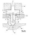
- Fig. 2a is the contact element 1 by means of a punch 14 which acts from above on the projections 4, has been inserted into a round hole 15 of a printed circuit board 16, wherein the pointed end portion 10 of the longer leg 5 a Introducer.
- the attachment portion 3 With the exception of its wedge surfaces 7, the attachment portion 3 has a cross section which is smaller than the diameter of the hole 15 on all sides.
- the hole 15 is formed by a tinned sleeve 17 which is inserted in the printed circuit board 16. The insertion process is almost powerless, because the legs 5, 6 with the exception of their wedge surfaces 7 without resistance can be inserted into the hole 15.
- a die 20 (forming tool) is pressed against the end portion 10 by a driving force, as indicated by the arrow 21.
- the longer leg 5 is bent to the left and partially bent until it finally abuts with its end face (hook surface) 22 against the end face 13 of the shorter leg 6 and this bends to the right and supported.
- the specially shaped die 20 supports this embossing or forming process.
- the embossment of the legs 5, 6 caused on the one hand, due to the eccentric load of the longer leg 5 and the specially shaped Gesenkgeometrie, a curling of the longer leg 5, on the other hand thereby the shorter leg 6 is displaced to the outside.
- Essential for the embossment is the expansion of the two legs 5, 6 in relation to the hole 15.
Landscapes
- Coupling Device And Connection With Printed Circuit (AREA)
- Multi-Conductor Connections (AREA)
Abstract
Description
Die Erfindung geht aus von einer elektrischen Kontaktanordnung nach der Gattung des Patentanspruchs 1.The invention is based on an electrical contact arrangement according to the preamble of patent claim 1.
Um Steckkontakte, z.B. Kontaktstifte, mit einer aus elektrisch isolierendem Material hergestellten Platine (auch Leiterplatte genannt) dauerhaft zu kontaktieren, wird Einpresstechnik eingesetzt. Ein runder, bolzenförmiger Befestigungsabschnitt des Kontaktelements wird in ein Leiterplattenloch gepresst, das durch eine in die Leiterplatte eingebrachte verzinnte Hülse gebildet ist. Die Einpresszone wird dabei plastisch und elastisch verformt, wodurch es an den Berührungsstellen zu einer dauerhaft festen Kaltverschweißung zwischen Metallteilen kommt. Beim Einpressen entstehen durch Abschälen Metallspäne, die Kurzschlüsse oder Nebenschlüsse (= hochohmige Kurzschlüsse) verursachen können. Außerdem kann durch die axiale Kraftbeaufschlagung während des Einpressprozesses die in die Leiterplatte eingebrachte verzinnte Hülse beschädigt werden, wodurch die Qualität der elektrischen Verbindung sofort oder erst nach langer Betriebszeit beeinträchtigt werden kann.In order to permanently contact plug-in contacts, eg contact pins, with a printed circuit board made of electrically insulating material (also called printed circuit board), press-fit technology is used. A round, bolt-shaped attachment portion of the contact element is pressed into a printed circuit board hole, which is formed by a tinned sleeve introduced into the circuit board. The press-in zone is plastically and elastically deformed, resulting in a permanently strong cold welding between metal parts at the points of contact. When pressed in, metal chips form due to peeling, which can cause short circuits or shunts (= high-resistance short circuits). In addition, by the axial application of force during the Einpressprozesses in the circuit board introduced tinned sleeve can be damaged, whereby the quality of the electrical connection can be affected immediately or only after a long period of operation.
Kaltverschweißung kann auch zwischen anderen Metallen auftreten, z. B. zwischen Gold-Gold und Kupfer-Kupfer. Wie auch Zinn, sind die zuletzt genannten Metalle im Zusammenhang mit der Herstellung von Leiterplatten bekannt. Der Ausdruck Zinn bedeutet in dieser Beschreibung eine Zinn enthaltende Legierung, die für elektrische Kontaktzwecke geeignet ist. Der Fachmann wählt eine für den gewünschten Anwendungsfall geeignete Zinnlegierung aus bekannten Legierungen aus.Cold welding can also occur between other metals, eg. B. between gold-gold and copper-copper. Like tin, the latter metals are known in connection with the production of printed circuit boards. The term tin in this specification means a tin-containing alloy suitable for electrical contact purposes. The person skilled in the art selects a tin alloy suitable for the desired application from known alloys.
Durch die
Aufgabe der Erfindung ist es, eine elektrische Kontaktanordnung zwischen einem Kontaktelement und einer Leiterplatte zu schaffen, die funktionssicher ist.The object of the invention is to provide an electrical contact arrangement between a contact element and a printed circuit board, which is functionally reliable.
Diese Aufgabe wird, ausgehend von einer elektrischen Kontaktanordnung entsprechend dem Oberbegriff des Anspruchs 1, durch die kennzeichnenden Merkmale des Anspruchs 1 gelöst.This object is achieved on the basis of an electrical contact arrangement according to the preamble of claim 1 by the characterizing features of claim 1.
Bei dieser Ausbildung der elektrischen Kontaktanordnung kommt ein Kontaktelement zur Anwendung, das beim Hindurchgreifen durch ein Loch einer Leiterplatte mit keiner oder geringer Kraftbeaufschlagung verbunden ist und danach mittels einer plastischen Umformung einen Hinterschnitt bildet. Damit werden Materialabschabungen bei der Herstellungen dieser Kontaktanordnung vermieden und eine funktionssichere Kontaktanordnung geschaffen.In this embodiment of the electrical contact arrangement, a contact element is used, which is connected when passing through a hole in a printed circuit board with no or little application of force and then forms an undercut by means of a plastic deformation. This material Abschschabungen be avoided in the preparation of this contact arrangement and created a functionally reliable contact arrangement.
Auch wird die Leiterplatte im Bereich der Kontaktierung deutlich weniger gestresst. Es ist eine hohe Kontaktsicherheit mit gutem Langzeitverhalten zu erwarten. Weiterhin sind prinzipiell große Haltekräfte möglich, da die Kontaktierzone des Befestigungsabschnitts nach der plastischen Umformung einen Hinterschnitt bildet. Wenn auch mehrere Metalle sich für Kaltverschweißungen eignen, wird Zinn bevorzugt.Also, the printed circuit board is significantly less stressed in the contact area. It is to be expected a high contact security with good long-term behavior. Furthermore, in principle, large holding forces are possible because the contacting of the mounting portion forms an undercut after the plastic deformation. Although several metals are suitable for cold welding, tin is preferred.
Weitere Vorteile und vorteilhafte Ausgestaltungen des Gegenstands der Erfindung sind der Beschreibung, der Zeichnung und den Ansprüchen entnehmbar.Further advantages and advantageous embodiments of the subject invention are the description, the drawings and claims removed.
Ein Ausführungsbeispiel des erfindungsgemäßen Kontaktelements ist in den Zeichnungen dargestellt und in der nachfolgenden Beschreibung näher erläutert. Die Figuren sind teilweise abgebrochen, schematisch und nicht maßstäblich. Es zeigen:
- Fig. 1
- die erfindungsgemäße elektrische Kontaktanordnung; und
- Fign. 2a, 2b
- ein in ein Leiterplattenloch eingesetztes Kontaktelement der Kontaktanordnung der
Fig. 1 vor dem Verprägen (Fig. 2a ) und nach dem Verprägen (Fig. 2b ).
- Fig. 1
- the electrical contact arrangement according to the invention; and
- FIGS. 2a, 2b
- an inserted into a PCB hole contact element of the contact arrangement of
Fig. 1 before embossing (Fig. 2a ) and after stamping (Fig. 2b ).
Das in
In
Nun wird von unten her ein Gesenk 20 (Umformwerkzeug) gegen den Endabschnitt 10 durch eine Antriebskraft gedrückt, wie durch den Pfeil 21 angedeutet ist. Dadurch wird der längere Schenkel 5 nach links gebogen und teilweise umgebogen, bis er schließlich mit seiner Endfläche (Hakenfläche) 22 gegen die Endfläche 13 des kürzeren Schenkels 6 stößt und diesen nach rechts umbiegt und abstützt. Das speziell geformte Gesenk 20 unterstützt diesen Prägevorgang oder Umformvorgang. Die Verprägung der Schenkel 5, 6 verursacht zum einen, bedingt durch die außermittige Belastung des längeren Schenkels 5 und die speziell geformte Gesenkgeometrie, ein Einrollen des längeren Schenkels 5, zum anderen wird hierdurch der kürzere Schenkel 6 nach außen verdrängt. Wesentlich für die Verprägung ist das Aufweiten der beiden Schenkel 5, 6 in Relation zum Loch 15. Hierdurch entsteht im Bereich des Loches 15 an der Leiterplattenunterseite ein Formschluss, der jede Relativbewegung zwischen dem Kontaktelement 1 und der Lochwand 18 verhindert. Dadurch wird, wie in
Alternativ oder zusätzlich zur außermittigen Anordnung der Spitze 11 bzw. des Endabschnitts 10 des längeren Schenkels 5 kann dieser auch auf seiner dem kürzeren Schenkel 6 zugewandten Seite eine in
Claims (9)
- Electrical contact arrangement having a printed circuit board (14) and having a metal contact element (1) which is connected to the latter and on which a contact-connection section (2) and a fastening section (3), which is intended to be connected to the printed circuit board (14), are formed, and the fastening section (3) has two limbs (5, 6) of different lengths which can be bent, extend essentially parallel to one another in the direction away from the contact-connection section (2) and engage through a hole (15) in the printed circuit board (14), wherein, after engaging through the hole (15), a longer limb (5) is designed in such a manner that, when its end section (10) which projects over a shorter limb (6) is subjected to compressive loading in the direction (21) of the contact-connection section (2), the longer limb (5) bends away from the shorter limb (6) and, with the end section (10), bends the shorter limb (6) away from the longer limb (5), characterized in that, after engaging through the hole (15), the two limbs (5, 6) of the contact element (1) are bent, in regions, in the direction away from one another so as to form a cold-welded connection (23) with a metal hole wall (18) of the hole (15) and the free ends of the two limbs (5, 6) then rest against one another.
- Electrical contact arrangement according to Claim 1, characterized in that, in the contact element (1), the end section (10) of the longer limb (5) laterally protrudes in the direction of the shorter limb (6), in particular laterally projects over the shorter limb (6).
- Electrical contact arrangement according to Claim 2, characterized in that the end section (10) of the longer limb (5) is bent in the form of a hook towards the shorter limb (6), in particular towards the end face (13) of the shorter limb (6).
- Electrical contact arrangement according to Claim 3, characterized in that the outermost end (11) of the end section (10) is arranged eccentrically with respect to the longer limb (5).
- Electrical contact arrangement according to Claim 4, characterized in that the longer limb (5) has a notch (25) on the side facing the shorter limb (6).
- Electrical contact arrangement according to Claim 5, characterized in that, on their ends facing the contact-connection region (2), the limbs (5, 6) each have, on their sides facing away from one another, wedge faces (7) which taper towards one another in the direction of the free limb ends.
- Electrical contact arrangement according to Claim 6, characterized in that the shorter limb (6) has an oblique end face (11) which faces the longer limb (5).
- Electrical contact arrangement according to Claim 7, characterized in that, on their ends facing the contact-connection region (2), the two limbs (5, 6) each have, on their sides facing away from one another, wedge faces (7) which taper towards one another in the direction of the free limb ends (10, 11) and are pressed into the metal hole wall (18) so as to form a further cold-welded connection (19).
- Electrical contact arrangement according to Claim 8, characterized in that the hole (15) in the printed circuit board (16) is formed by a metal sleeve (17), in particular a tin-plated sleeve.
Applications Claiming Priority (1)
| Application Number | Priority Date | Filing Date | Title |
|---|---|---|---|
| DE102006041978A DE102006041978A1 (en) | 2006-09-07 | 2006-09-07 | Metallic contact element for an electrical contact arrangement |
Publications (2)
| Publication Number | Publication Date |
|---|---|
| EP1898496A1 EP1898496A1 (en) | 2008-03-12 |
| EP1898496B1 true EP1898496B1 (en) | 2010-09-22 |
Family
ID=38786922
Family Applications (1)
| Application Number | Title | Priority Date | Filing Date |
|---|---|---|---|
| EP07112126A Not-in-force EP1898496B1 (en) | 2006-09-07 | 2007-07-10 | Metal contact element for an electric contact assembly |
Country Status (3)
| Country | Link |
|---|---|
| EP (1) | EP1898496B1 (en) |
| AT (1) | ATE482495T1 (en) |
| DE (2) | DE102006041978A1 (en) |
Families Citing this family (3)
| Publication number | Priority date | Publication date | Assignee | Title |
|---|---|---|---|---|
| DE102007014356A1 (en) | 2007-03-26 | 2008-10-02 | Robert Bosch Gmbh | Pin for insertion into a receiving opening of a printed circuit board and method for inserting a pin in a receiving opening of a printed circuit board |
| DE102011005497A1 (en) * | 2011-03-14 | 2012-09-20 | Continental Automotive Gmbh | Electrical plug connector e.g. fixing pin, for engine controller utilized for motor car, has connection section inserted into through-hole of circuit board without deformation and electrically interconnected with board in gastight manner |
| JP7195644B2 (en) * | 2020-10-02 | 2022-12-26 | 株式会社シンエイ・ハイテック | press fit terminal |
Family Cites Families (3)
| Publication number | Priority date | Publication date | Assignee | Title |
|---|---|---|---|---|
| NL129068C (en) * | 1900-01-01 | |||
| US5282758A (en) | 1988-11-11 | 1994-02-01 | Amp Incorporated | Electrical contact |
| FR2824427A1 (en) * | 2001-05-07 | 2002-11-08 | Cartier Technologies G | Connection terminal for printed circuit and system for its integration comprises cutout flat plate with cross-link, projecting and contact legs |
-
2006
- 2006-09-07 DE DE102006041978A patent/DE102006041978A1/en not_active Withdrawn
-
2007
- 2007-07-10 EP EP07112126A patent/EP1898496B1/en not_active Not-in-force
- 2007-07-10 DE DE502007005128T patent/DE502007005128D1/en active Active
- 2007-07-10 AT AT07112126T patent/ATE482495T1/en active
Also Published As
| Publication number | Publication date |
|---|---|
| ATE482495T1 (en) | 2010-10-15 |
| DE502007005128D1 (en) | 2010-11-04 |
| DE102006041978A1 (en) | 2008-03-27 |
| EP1898496A1 (en) | 2008-03-12 |
Similar Documents
| Publication | Publication Date | Title |
|---|---|---|
| EP2130418B1 (en) | Method for inserting a pin into a receiving opening in a circuit board | |
| EP1754285B1 (en) | Press-in contact | |
| EP1997187A1 (en) | Contact pin and method for its production | |
| EP0059462B1 (en) | Pressurized connection pin | |
| DE68923016T2 (en) | Electrical tail pin with compliant part. | |
| WO2011072643A1 (en) | Contact device for fastening to a circuit board, method for fastening a contact device to a circuit board, and circuit board | |
| DE102014208101A1 (en) | Electrical connection arrangement for the electrical connection of printed circuit boards with each other by means of solder-free press-fitting | |
| DE102013209407A1 (en) | Method for solderless electrical press-in contacting of electrically conductive press-fit pins in printed circuit boards | |
| EP3022805A1 (en) | Contact device for establishing an electrical connection to a contact point of a printed circuit board | |
| EP3243246B1 (en) | Electrical functional component having a contact pin, and method for producing an electrical functional component | |
| DE112009004576B4 (en) | A connector connection structure for electrically connecting a connector terminal to an electrode surface of a panel and light emitting device therewith | |
| EP3036796B1 (en) | Electrical contact arrangement for an electric motor and method for producing same | |
| EP1898496B1 (en) | Metal contact element for an electric contact assembly | |
| DE102005062709A1 (en) | Electrical connection | |
| EP3349307A1 (en) | Electrical press-in contact element | |
| DE102017125505A1 (en) | Socket for printed circuit boards | |
| EP2259380A1 (en) | Connection device and method for producing same | |
| DE102011051231B4 (en) | Terminal body, electrical connection terminal and method for producing a terminal body | |
| DE102020106194A1 (en) | Electrical connector and method of making an electrical connector | |
| WO2010076167A1 (en) | Plug connector for a blade contact | |
| EP4282034A1 (en) | Current connector for circuit boards | |
| EP2614559B1 (en) | Method for producing pin-shaped contact elements and contact element | |
| DE102020120086A1 (en) | FASTENING A FLAT CONDUCTOR IN AN ELECTRICAL ASSEMBLY | |
| WO2020228974A1 (en) | Wire-connecting element | |
| DE10130618B4 (en) | Method for equipping a carrier with a component and device for connecting the same |
Legal Events
| Date | Code | Title | Description |
|---|---|---|---|
| PUAI | Public reference made under article 153(3) epc to a published international application that has entered the european phase |
Free format text: ORIGINAL CODE: 0009012 |
|
| AK | Designated contracting states |
Kind code of ref document: A1 Designated state(s): AT BE BG CH CY CZ DE DK EE ES FI FR GB GR HU IE IS IT LI LT LU LV MC MT NL PL PT RO SE SI SK TR |
|
| AX | Request for extension of the european patent |
Extension state: AL BA HR MK YU |
|
| 17P | Request for examination filed |
Effective date: 20080912 |
|
| 17Q | First examination report despatched |
Effective date: 20081010 |
|
| AKX | Designation fees paid |
Designated state(s): AT BE BG CH CY CZ DE DK EE ES FI FR GB GR HU IE IS IT LI LT LU LV MC MT NL PL PT RO SE SI SK TR |
|
| GRAP | Despatch of communication of intention to grant a patent |
Free format text: ORIGINAL CODE: EPIDOSNIGR1 |
|
| GRAS | Grant fee paid |
Free format text: ORIGINAL CODE: EPIDOSNIGR3 |
|
| GRAA | (expected) grant |
Free format text: ORIGINAL CODE: 0009210 |
|
| AK | Designated contracting states |
Kind code of ref document: B1 Designated state(s): AT BE BG CH CY CZ DE DK EE ES FI FR GB GR HU IE IS IT LI LT LU LV MC MT NL PL PT RO SE SI SK TR |
|
| REG | Reference to a national code |
Ref country code: GB Ref legal event code: FG4D Free format text: NOT ENGLISH |
|
| REG | Reference to a national code |
Ref country code: CH Ref legal event code: EP |
|
| REG | Reference to a national code |
Ref country code: IE Ref legal event code: FG4D Free format text: LANGUAGE OF EP DOCUMENT: GERMAN |
|
| REF | Corresponds to: |
Ref document number: 502007005128 Country of ref document: DE Date of ref document: 20101104 Kind code of ref document: P |
|
| PG25 | Lapsed in a contracting state [announced via postgrant information from national office to epo] |
Ref country code: FI Free format text: LAPSE BECAUSE OF FAILURE TO SUBMIT A TRANSLATION OF THE DESCRIPTION OR TO PAY THE FEE WITHIN THE PRESCRIBED TIME-LIMIT Effective date: 20100922 Ref country code: LT Free format text: LAPSE BECAUSE OF FAILURE TO SUBMIT A TRANSLATION OF THE DESCRIPTION OR TO PAY THE FEE WITHIN THE PRESCRIBED TIME-LIMIT Effective date: 20100922 |
|
| REG | Reference to a national code |
Ref country code: NL Ref legal event code: VDEP Effective date: 20100922 |
|
| LTIE | Lt: invalidation of european patent or patent extension |
Effective date: 20100922 |
|
| PG25 | Lapsed in a contracting state [announced via postgrant information from national office to epo] |
Ref country code: SI Free format text: LAPSE BECAUSE OF FAILURE TO SUBMIT A TRANSLATION OF THE DESCRIPTION OR TO PAY THE FEE WITHIN THE PRESCRIBED TIME-LIMIT Effective date: 20100922 Ref country code: PL Free format text: LAPSE BECAUSE OF FAILURE TO SUBMIT A TRANSLATION OF THE DESCRIPTION OR TO PAY THE FEE WITHIN THE PRESCRIBED TIME-LIMIT Effective date: 20100922 |
|
| PG25 | Lapsed in a contracting state [announced via postgrant information from national office to epo] |
Ref country code: LV Free format text: LAPSE BECAUSE OF FAILURE TO SUBMIT A TRANSLATION OF THE DESCRIPTION OR TO PAY THE FEE WITHIN THE PRESCRIBED TIME-LIMIT Effective date: 20100922 Ref country code: SE Free format text: LAPSE BECAUSE OF FAILURE TO SUBMIT A TRANSLATION OF THE DESCRIPTION OR TO PAY THE FEE WITHIN THE PRESCRIBED TIME-LIMIT Effective date: 20100922 Ref country code: GR Free format text: LAPSE BECAUSE OF FAILURE TO SUBMIT A TRANSLATION OF THE DESCRIPTION OR TO PAY THE FEE WITHIN THE PRESCRIBED TIME-LIMIT Effective date: 20101223 |
|
| REG | Reference to a national code |
Ref country code: IE Ref legal event code: FD4D |
|
| PG25 | Lapsed in a contracting state [announced via postgrant information from national office to epo] |
Ref country code: IE Free format text: LAPSE BECAUSE OF FAILURE TO SUBMIT A TRANSLATION OF THE DESCRIPTION OR TO PAY THE FEE WITHIN THE PRESCRIBED TIME-LIMIT Effective date: 20100922 |
|
| PG25 | Lapsed in a contracting state [announced via postgrant information from national office to epo] |
Ref country code: NL Free format text: LAPSE BECAUSE OF FAILURE TO SUBMIT A TRANSLATION OF THE DESCRIPTION OR TO PAY THE FEE WITHIN THE PRESCRIBED TIME-LIMIT Effective date: 20100922 Ref country code: EE Free format text: LAPSE BECAUSE OF FAILURE TO SUBMIT A TRANSLATION OF THE DESCRIPTION OR TO PAY THE FEE WITHIN THE PRESCRIBED TIME-LIMIT Effective date: 20100922 Ref country code: IS Free format text: LAPSE BECAUSE OF FAILURE TO SUBMIT A TRANSLATION OF THE DESCRIPTION OR TO PAY THE FEE WITHIN THE PRESCRIBED TIME-LIMIT Effective date: 20110122 Ref country code: PT Free format text: LAPSE BECAUSE OF FAILURE TO SUBMIT A TRANSLATION OF THE DESCRIPTION OR TO PAY THE FEE WITHIN THE PRESCRIBED TIME-LIMIT Effective date: 20110124 Ref country code: RO Free format text: LAPSE BECAUSE OF FAILURE TO SUBMIT A TRANSLATION OF THE DESCRIPTION OR TO PAY THE FEE WITHIN THE PRESCRIBED TIME-LIMIT Effective date: 20100922 Ref country code: SK Free format text: LAPSE BECAUSE OF FAILURE TO SUBMIT A TRANSLATION OF THE DESCRIPTION OR TO PAY THE FEE WITHIN THE PRESCRIBED TIME-LIMIT Effective date: 20100922 |
|
| PG25 | Lapsed in a contracting state [announced via postgrant information from national office to epo] |
Ref country code: ES Free format text: LAPSE BECAUSE OF FAILURE TO SUBMIT A TRANSLATION OF THE DESCRIPTION OR TO PAY THE FEE WITHIN THE PRESCRIBED TIME-LIMIT Effective date: 20110102 |
|
| PLBE | No opposition filed within time limit |
Free format text: ORIGINAL CODE: 0009261 |
|
| STAA | Information on the status of an ep patent application or granted ep patent |
Free format text: STATUS: NO OPPOSITION FILED WITHIN TIME LIMIT |
|
| 26N | No opposition filed |
Effective date: 20110623 |
|
| PG25 | Lapsed in a contracting state [announced via postgrant information from national office to epo] |
Ref country code: DK Free format text: LAPSE BECAUSE OF FAILURE TO SUBMIT A TRANSLATION OF THE DESCRIPTION OR TO PAY THE FEE WITHIN THE PRESCRIBED TIME-LIMIT Effective date: 20100922 |
|
| REG | Reference to a national code |
Ref country code: DE Ref legal event code: R097 Ref document number: 502007005128 Country of ref document: DE Effective date: 20110623 |
|
| PG25 | Lapsed in a contracting state [announced via postgrant information from national office to epo] |
Ref country code: MT Free format text: LAPSE BECAUSE OF FAILURE TO SUBMIT A TRANSLATION OF THE DESCRIPTION OR TO PAY THE FEE WITHIN THE PRESCRIBED TIME-LIMIT Effective date: 20100922 |
|
| BERE | Be: lapsed |
Owner name: ROBERT BOSCH G.M.B.H. Effective date: 20110731 |
|
| PG25 | Lapsed in a contracting state [announced via postgrant information from national office to epo] |
Ref country code: MC Free format text: LAPSE BECAUSE OF NON-PAYMENT OF DUE FEES Effective date: 20110731 |
|
| REG | Reference to a national code |
Ref country code: CH Ref legal event code: PL |
|
| GBPC | Gb: european patent ceased through non-payment of renewal fee |
Effective date: 20110710 |
|
| PG25 | Lapsed in a contracting state [announced via postgrant information from national office to epo] |
Ref country code: BE Free format text: LAPSE BECAUSE OF NON-PAYMENT OF DUE FEES Effective date: 20110731 Ref country code: CH Free format text: LAPSE BECAUSE OF NON-PAYMENT OF DUE FEES Effective date: 20110731 Ref country code: LI Free format text: LAPSE BECAUSE OF NON-PAYMENT OF DUE FEES Effective date: 20110731 |
|
| PG25 | Lapsed in a contracting state [announced via postgrant information from national office to epo] |
Ref country code: GB Free format text: LAPSE BECAUSE OF NON-PAYMENT OF DUE FEES Effective date: 20110710 |
|
| PG25 | Lapsed in a contracting state [announced via postgrant information from national office to epo] |
Ref country code: LU Free format text: LAPSE BECAUSE OF NON-PAYMENT OF DUE FEES Effective date: 20110710 Ref country code: CY Free format text: LAPSE BECAUSE OF EXPIRATION OF PROTECTION Effective date: 20100922 |
|
| REG | Reference to a national code |
Ref country code: AT Ref legal event code: MM01 Ref document number: 482495 Country of ref document: AT Kind code of ref document: T Effective date: 20120731 |
|
| PG25 | Lapsed in a contracting state [announced via postgrant information from national office to epo] |
Ref country code: BG Free format text: LAPSE BECAUSE OF FAILURE TO SUBMIT A TRANSLATION OF THE DESCRIPTION OR TO PAY THE FEE WITHIN THE PRESCRIBED TIME-LIMIT Effective date: 20101222 Ref country code: TR Free format text: LAPSE BECAUSE OF FAILURE TO SUBMIT A TRANSLATION OF THE DESCRIPTION OR TO PAY THE FEE WITHIN THE PRESCRIBED TIME-LIMIT Effective date: 20100922 |
|
| PG25 | Lapsed in a contracting state [announced via postgrant information from national office to epo] |
Ref country code: HU Free format text: LAPSE BECAUSE OF FAILURE TO SUBMIT A TRANSLATION OF THE DESCRIPTION OR TO PAY THE FEE WITHIN THE PRESCRIBED TIME-LIMIT Effective date: 20100922 Ref country code: AT Free format text: LAPSE BECAUSE OF NON-PAYMENT OF DUE FEES Effective date: 20120731 |
|
| PGFP | Annual fee paid to national office [announced via postgrant information from national office to epo] |
Ref country code: FR Payment date: 20140724 Year of fee payment: 8 |
|
| PGFP | Annual fee paid to national office [announced via postgrant information from national office to epo] |
Ref country code: IT Payment date: 20140724 Year of fee payment: 8 |
|
| PG25 | Lapsed in a contracting state [announced via postgrant information from national office to epo] |
Ref country code: IT Free format text: LAPSE BECAUSE OF NON-PAYMENT OF DUE FEES Effective date: 20150710 |
|
| PGFP | Annual fee paid to national office [announced via postgrant information from national office to epo] |
Ref country code: CZ Payment date: 20160108 Year of fee payment: 9 |
|
| REG | Reference to a national code |
Ref country code: FR Ref legal event code: ST Effective date: 20160331 |
|
| PG25 | Lapsed in a contracting state [announced via postgrant information from national office to epo] |
Ref country code: FR Free format text: LAPSE BECAUSE OF NON-PAYMENT OF DUE FEES Effective date: 20150731 |
|
| PG25 | Lapsed in a contracting state [announced via postgrant information from national office to epo] |
Ref country code: CZ Free format text: LAPSE BECAUSE OF NON-PAYMENT OF DUE FEES Effective date: 20160710 |
|
| PGFP | Annual fee paid to national office [announced via postgrant information from national office to epo] |
Ref country code: DE Payment date: 20210924 Year of fee payment: 15 |
|
| REG | Reference to a national code |
Ref country code: DE Ref legal event code: R119 Ref document number: 502007005128 Country of ref document: DE |
|
| PG25 | Lapsed in a contracting state [announced via postgrant information from national office to epo] |
Ref country code: DE Free format text: LAPSE BECAUSE OF NON-PAYMENT OF DUE FEES Effective date: 20230201 |