EP3242288A1 - Data drive circuit and drive method therefor, and organic light emitting display - Google Patents
Data drive circuit and drive method therefor, and organic light emitting display Download PDFInfo
- Publication number
- EP3242288A1 EP3242288A1 EP15875110.7A EP15875110A EP3242288A1 EP 3242288 A1 EP3242288 A1 EP 3242288A1 EP 15875110 A EP15875110 A EP 15875110A EP 3242288 A1 EP3242288 A1 EP 3242288A1
- Authority
- EP
- European Patent Office
- Prior art keywords
- data
- line
- column
- drive circuit
- lines
- Prior art date
- Legal status (The legal status is an assumption and is not a legal conclusion. Google has not performed a legal analysis and makes no representation as to the accuracy of the status listed.)
- Ceased
Links
Images


Classifications
-
- G—PHYSICS
- G09—EDUCATION; CRYPTOGRAPHY; DISPLAY; ADVERTISING; SEALS
- G09G—ARRANGEMENTS OR CIRCUITS FOR CONTROL OF INDICATING DEVICES USING STATIC MEANS TO PRESENT VARIABLE INFORMATION
- G09G3/00—Control arrangements or circuits, of interest only in connection with visual indicators other than cathode-ray tubes
- G09G3/20—Control arrangements or circuits, of interest only in connection with visual indicators other than cathode-ray tubes for presentation of an assembly of a number of characters, e.g. a page, by composing the assembly by combination of individual elements arranged in a matrix no fixed position being assigned to or needed to be assigned to the individual characters or partial characters
- G09G3/22—Control arrangements or circuits, of interest only in connection with visual indicators other than cathode-ray tubes for presentation of an assembly of a number of characters, e.g. a page, by composing the assembly by combination of individual elements arranged in a matrix no fixed position being assigned to or needed to be assigned to the individual characters or partial characters using controlled light sources
- G09G3/30—Control arrangements or circuits, of interest only in connection with visual indicators other than cathode-ray tubes for presentation of an assembly of a number of characters, e.g. a page, by composing the assembly by combination of individual elements arranged in a matrix no fixed position being assigned to or needed to be assigned to the individual characters or partial characters using controlled light sources using electroluminescent panels
- G09G3/32—Control arrangements or circuits, of interest only in connection with visual indicators other than cathode-ray tubes for presentation of an assembly of a number of characters, e.g. a page, by composing the assembly by combination of individual elements arranged in a matrix no fixed position being assigned to or needed to be assigned to the individual characters or partial characters using controlled light sources using electroluminescent panels semiconductive, e.g. using light-emitting diodes [LED]
- G09G3/3208—Control arrangements or circuits, of interest only in connection with visual indicators other than cathode-ray tubes for presentation of an assembly of a number of characters, e.g. a page, by composing the assembly by combination of individual elements arranged in a matrix no fixed position being assigned to or needed to be assigned to the individual characters or partial characters using controlled light sources using electroluminescent panels semiconductive, e.g. using light-emitting diodes [LED] organic, e.g. using organic light-emitting diodes [OLED]
- G09G3/3275—Details of drivers for data electrodes
-
- G—PHYSICS
- G09—EDUCATION; CRYPTOGRAPHY; DISPLAY; ADVERTISING; SEALS
- G09G—ARRANGEMENTS OR CIRCUITS FOR CONTROL OF INDICATING DEVICES USING STATIC MEANS TO PRESENT VARIABLE INFORMATION
- G09G3/00—Control arrangements or circuits, of interest only in connection with visual indicators other than cathode-ray tubes
- G09G3/20—Control arrangements or circuits, of interest only in connection with visual indicators other than cathode-ray tubes for presentation of an assembly of a number of characters, e.g. a page, by composing the assembly by combination of individual elements arranged in a matrix no fixed position being assigned to or needed to be assigned to the individual characters or partial characters
- G09G3/22—Control arrangements or circuits, of interest only in connection with visual indicators other than cathode-ray tubes for presentation of an assembly of a number of characters, e.g. a page, by composing the assembly by combination of individual elements arranged in a matrix no fixed position being assigned to or needed to be assigned to the individual characters or partial characters using controlled light sources
- G09G3/30—Control arrangements or circuits, of interest only in connection with visual indicators other than cathode-ray tubes for presentation of an assembly of a number of characters, e.g. a page, by composing the assembly by combination of individual elements arranged in a matrix no fixed position being assigned to or needed to be assigned to the individual characters or partial characters using controlled light sources using electroluminescent panels
- G09G3/32—Control arrangements or circuits, of interest only in connection with visual indicators other than cathode-ray tubes for presentation of an assembly of a number of characters, e.g. a page, by composing the assembly by combination of individual elements arranged in a matrix no fixed position being assigned to or needed to be assigned to the individual characters or partial characters using controlled light sources using electroluminescent panels semiconductive, e.g. using light-emitting diodes [LED]
- G09G3/3208—Control arrangements or circuits, of interest only in connection with visual indicators other than cathode-ray tubes for presentation of an assembly of a number of characters, e.g. a page, by composing the assembly by combination of individual elements arranged in a matrix no fixed position being assigned to or needed to be assigned to the individual characters or partial characters using controlled light sources using electroluminescent panels semiconductive, e.g. using light-emitting diodes [LED] organic, e.g. using organic light-emitting diodes [OLED]
- G09G3/3225—Control arrangements or circuits, of interest only in connection with visual indicators other than cathode-ray tubes for presentation of an assembly of a number of characters, e.g. a page, by composing the assembly by combination of individual elements arranged in a matrix no fixed position being assigned to or needed to be assigned to the individual characters or partial characters using controlled light sources using electroluminescent panels semiconductive, e.g. using light-emitting diodes [LED] organic, e.g. using organic light-emitting diodes [OLED] using an active matrix
-
- G—PHYSICS
- G09—EDUCATION; CRYPTOGRAPHY; DISPLAY; ADVERTISING; SEALS
- G09G—ARRANGEMENTS OR CIRCUITS FOR CONTROL OF INDICATING DEVICES USING STATIC MEANS TO PRESENT VARIABLE INFORMATION
- G09G2230/00—Details of flat display driving waveforms
-
- G—PHYSICS
- G09—EDUCATION; CRYPTOGRAPHY; DISPLAY; ADVERTISING; SEALS
- G09G—ARRANGEMENTS OR CIRCUITS FOR CONTROL OF INDICATING DEVICES USING STATIC MEANS TO PRESENT VARIABLE INFORMATION
- G09G2310/00—Command of the display device
- G09G2310/02—Addressing, scanning or driving the display screen or processing steps related thereto
- G09G2310/0243—Details of the generation of driving signals
- G09G2310/0248—Precharge or discharge of column electrodes before or after applying exact column voltages
-
- G—PHYSICS
- G09—EDUCATION; CRYPTOGRAPHY; DISPLAY; ADVERTISING; SEALS
- G09G—ARRANGEMENTS OR CIRCUITS FOR CONTROL OF INDICATING DEVICES USING STATIC MEANS TO PRESENT VARIABLE INFORMATION
- G09G2310/00—Command of the display device
- G09G2310/02—Addressing, scanning or driving the display screen or processing steps related thereto
- G09G2310/0264—Details of driving circuits
- G09G2310/0297—Special arrangements with multiplexing or demultiplexing of display data in the drivers for data electrodes, in a pre-processing circuitry delivering display data to said drivers or in the matrix panel, e.g. multiplexing plural data signals to one D/A converter or demultiplexing the D/A converter output to multiple columns
-
- G—PHYSICS
- G09—EDUCATION; CRYPTOGRAPHY; DISPLAY; ADVERTISING; SEALS
- G09G—ARRANGEMENTS OR CIRCUITS FOR CONTROL OF INDICATING DEVICES USING STATIC MEANS TO PRESENT VARIABLE INFORMATION
- G09G2310/00—Command of the display device
- G09G2310/08—Details of timing specific for flat panels, other than clock recovery
-
- G—PHYSICS
- G09—EDUCATION; CRYPTOGRAPHY; DISPLAY; ADVERTISING; SEALS
- G09G—ARRANGEMENTS OR CIRCUITS FOR CONTROL OF INDICATING DEVICES USING STATIC MEANS TO PRESENT VARIABLE INFORMATION
- G09G2320/00—Control of display operating conditions
- G09G2320/02—Improving the quality of display appearance
- G09G2320/0252—Improving the response speed
-
- G—PHYSICS
- G09—EDUCATION; CRYPTOGRAPHY; DISPLAY; ADVERTISING; SEALS
- G09G—ARRANGEMENTS OR CIRCUITS FOR CONTROL OF INDICATING DEVICES USING STATIC MEANS TO PRESENT VARIABLE INFORMATION
- G09G2330/00—Aspects of power supply; Aspects of display protection and defect management
- G09G2330/02—Details of power systems and of start or stop of display operation
-
- G—PHYSICS
- G09—EDUCATION; CRYPTOGRAPHY; DISPLAY; ADVERTISING; SEALS
- G09G—ARRANGEMENTS OR CIRCUITS FOR CONTROL OF INDICATING DEVICES USING STATIC MEANS TO PRESENT VARIABLE INFORMATION
- G09G3/00—Control arrangements or circuits, of interest only in connection with visual indicators other than cathode-ray tubes
- G09G3/20—Control arrangements or circuits, of interest only in connection with visual indicators other than cathode-ray tubes for presentation of an assembly of a number of characters, e.g. a page, by composing the assembly by combination of individual elements arranged in a matrix no fixed position being assigned to or needed to be assigned to the individual characters or partial characters
- G09G3/22—Control arrangements or circuits, of interest only in connection with visual indicators other than cathode-ray tubes for presentation of an assembly of a number of characters, e.g. a page, by composing the assembly by combination of individual elements arranged in a matrix no fixed position being assigned to or needed to be assigned to the individual characters or partial characters using controlled light sources
- G09G3/30—Control arrangements or circuits, of interest only in connection with visual indicators other than cathode-ray tubes for presentation of an assembly of a number of characters, e.g. a page, by composing the assembly by combination of individual elements arranged in a matrix no fixed position being assigned to or needed to be assigned to the individual characters or partial characters using controlled light sources using electroluminescent panels
- G09G3/32—Control arrangements or circuits, of interest only in connection with visual indicators other than cathode-ray tubes for presentation of an assembly of a number of characters, e.g. a page, by composing the assembly by combination of individual elements arranged in a matrix no fixed position being assigned to or needed to be assigned to the individual characters or partial characters using controlled light sources using electroluminescent panels semiconductive, e.g. using light-emitting diodes [LED]
- G09G3/3208—Control arrangements or circuits, of interest only in connection with visual indicators other than cathode-ray tubes for presentation of an assembly of a number of characters, e.g. a page, by composing the assembly by combination of individual elements arranged in a matrix no fixed position being assigned to or needed to be assigned to the individual characters or partial characters using controlled light sources using electroluminescent panels semiconductive, e.g. using light-emitting diodes [LED] organic, e.g. using organic light-emitting diodes [OLED]
- G09G3/3266—Details of drivers for scan electrodes
Definitions
- AMOLED Active Matrix Organic Light Emitting Display
- OLED Organic Light Emitting Diode
- a large type Active Matrix Organic Light Emitting Display apparatus comprises a plurality of pixel units located in areas with crossed scan lines and data lines.
- a traditional Active Matrix Organic Light Emitting Display panel comprises a data driver 20, a scan driver 30 and pixel units 11, 12 ... nm.
- the data signal sent from the data driver 20 is provided by a drive chip, usually, one column of pixel units require one data signal, and m columns of pixel units require m data signals D1, D2 ... Dm.
- a drive chip usually, one column of pixel units require one data signal, and m columns of pixel units require m data signals D1, D2 ... Dm.
- the cost of a drive chip is high and is proportional to the area of the drive chip, more data signals would take more chip area and thus increase the cost of the drive chip. Therefore, many companies use data signal multiplexing (Mux/Demux) configurations to reduce the number of drive signals, so as to reduce the area of the drive chip and thus reduce the cost of the
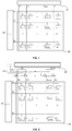
- FIG. 2 is a schematic diagram of an AMOLED panel that uses a data signal multiplexing configuration, which adds m P-type switch transistors and two other switch transistors to control signals of Sel_1 and Sel_2.
- the number of data signal lines of the data driver is reduced by half, from m to m/2.
- a switch transistor T1 in a data signal write cycle T1 of the first column of data line: within the time period t1, a switch transistor T1 is switched on, and a high level signal (5V) on a data signal line D1 is transmitted to a signal line D1' in the display area; within the time period t2, a switch transistor T2 is switched on, and the high level signal on the data signal line D1 is transmitted to a signal line D2' in the display area.
- a data signal write cycle T2 of the second column of data line within the time period t3, the switch transistor T1 is switched on, a low level on the data signal line D1 is transmitted to the signal line D1' in the display area, so that the pixel unit 21 is loaded with low level; at this time, the signal line D2' is in a suspended state, and because of existence of signal line stray capacitance, the signal line D2' would keep the high level status attained in the time period t1, so that the pixel unit 22 is loaded with high level.
- the switch transistor T2 is switched on to transmit the low level signal on the data signal line D1 to the signal line D2' in the display area, however, because the pixel unit 22 has already been loaded with high level in the time period t3, the pixel unit 22 cannot effectively receive a low level signal, as a result, the AMOLED panel shows a phenomenon of display abnormality.
- the drive chip area may be reduced, so that the production cost is reduced, there is still a problem of response delay which leads to display abnormality.
- the present invention intends to solve the problem that the existing data drive circuits of AMOLED have response delay which leads to display abnormality, by providing a data drive circuit and its drive method and application that can effectively improve the response properties of a display apparatus.
- the first transistor and second transistor connected to the same signal line have gate electrodes connected to different lines of the control lines.
- the power source has a voltage value lower than or equal to 0V.
- all of the first transistors are P-type transistors.
- all of the second transistors are field effect transistors with the same channel polarity.
- the second transistors are P-type field effect transistors.
- a drive method for the data drive circuit in accordance with the present invention comprises dividing the data signal write cycle of each column of data line into i time periods; sequentially setting each of the control lines to be low level in each of the time periods; in the first of the time periods, the second transistor connected to the control line set at low level is switched on, so that the signal line connected to this second transistor is connected to the power source, and the pixel units in the column corresponding to this signal line is initialized.
- the first transistor connected to the control line set at low level is switched on, so that the signal line connected to this first transistor is connected to the data line, and signal is written into the pixel units in the column corresponding to this signal line.
- the voltage for the initialization is lower than or equal to 0V.
- An organic light emitting display in accordance with the present invention comprises the above-mentioned data drive circuit.
- the data drive circuit in accordance with embodiments of the present invention is electrically connected to a data driver via data lines, and electrically connected to a scan driver via scan lines, wherein, each data line is connected to i columns of signal lines at an end away from the data driver, each row of the scan lines is electrically connected to a corresponding row of pixel units arranged in a display area, each column of the signal lines is electrically connected to a corresponding column of pixel units arranged in the display area; a first transistor is connected in a segment within each signal line between the data line and the display area, said data drive circuit further comprises control lines connected to the data driver; the i first transistors connected to the same data line respectively have gate electrodes electrically connected to different lines of the control lines; said data drive circuit further comprises a power source line and m(i-1)/i second transistors, namely m-m/i second transistors, connected to the power source line, the power source line is connected to a power source; the respective second transistors have source electrodes all electrically connected to the
- first unit when a first unit is described to be "connected" to a second unit, the first unit may be directly connected to the second unit, or may be indirectly connected to the second unit via one or more additional units. Furthermore, for the sake of clarity, some elements that are not necessary for fully understanding the present invention are omitted. Also, the same reference sign always refers to the same unit.
- the data drive circuit also comprises pixel units 11, 12, 13 ...
- each row of the scan lines S1, S2 ... Sn is electrically connected to a corresponding row of pixel units arranged in the display area 40, each column of the signal lines D1', D2' ...
- D(m-1)', Dm' is electrically connected to a corresponding column of pixel units arranged in the display area 40, that is to say, a number m column of signal line Dm' and a number n row of scan line Sn are connected to a pixel unit nm at Row n Column m.
- a first transistor T1, T2 ... T(m-1), Tm is respectively connected in a segment within each of the signal lines D1', D2' ... D(m-1)', Dm' between each of the data lines D1 ... D(m/2) and the display area 40, said data drive circuit further comprises 2 rows of control lines Sel_1, Sel_2 connected to the data driver 20.
- These first transistors T1, T2 ... T(m-1), Tm are preferably P-type transistors.
- the data drive circuit further comprises a power source line 50 and m/2 second transistors T2' ... Tm' connected to the power source line 50, the power source line 50 is connected to a power source Vref.
- the power source Vref has a voltage value lower than or equal to 0V, and preferable has a voltage of 0V in this embodiment.
- the respective second transistors T2' ... Tm' have source electrodes all electrically connected to the power source line 50, and gate electrodes electrically connected to the same line Sel_1 of the control lines.
- the first transistor T2, T4 ... T(m-2), Tm and the second transistor T2', T4' ... T(m-2)', Tm' connected to the same signal line D2', D4' ... D(m-2)', Dm' have their gate electrodes connected to different lines of the control lines, which are Sel_1, Sel_2 in this embodiment.
- the gate electrode of the second column of second transistor T2' is electrically connected to the control line Sel_1, while the gate electrode of the first transistor T2 in the same column is electrically connected to the control line Sel_2; ...the gate electrode of the number m column of second transistor Tm' is electrically connected to the control line Sel_1, while the gate electrode of the first transistor Tm in the same column is electrically connected to the control line Sel_2.
- All of the second transistors T2' ... Tm' are field effect transistors with the same channel polarity, and are preferably P-type field effect transistors in this embodiment.
- i time periods preferably 2 time periods (t1, t2) in this embodiment.
- the control line Sel_1 has low level
- the control line Sel_2 has high level
- the first column of first transistor T1 and the second column of second transistor T2' are switched on, while the second column of first transistor T2 is switched off
- the high level on the first column of data line D1 is transmitted to the first column of signal line D1' in the display area 40, and then the data signal on the signal line D1' is loaded onto the first column of pixel units 11, 21 ... n1
- the second column of signal line D2' is connected to the power source Vref, so that the second column of signal line D2' is initialized and the voltage loaded onto the second column of pixel units 12, 22 ... n2 is 0V.
- the control line Sel_2 has low level, the control line Sel_1 has high level, the second column of first transistor T2 is switched on, while the first column of first transistor T1 and the second column of second transistor T2' are switched off; the high level on the first column of data line D1 is transmitted to the second column of signal line D2' in the display area 40, and then the data signal on the signal line D2' is loaded onto the second column of pixel units 12, 22 ... n2.
- the first column of data line D1 transmits low level.
- the control line Sel_1 has low level
- the control line Sel_2 has high level
- the first column of first transistor T1 and the second column of second transistor T2' are switched on, while the second column of first transistor T2 is switched off
- the low level on the first column of data line D1 is transmitted to the first column of signal line D1' in the display area 40, and the first column of pixel units 11, 21 ... n1 are loaded with low level
- the second column of signal line D2' is connected to the power source Vref, so that the high level on the second column of pixel units 12, 22 ... n2 that is attained in the data signal write cycle T1 becomes initialized to 0V.
- the control line Sel_2 has low level, the control line Sel_1 has high level, the second column of first transistor T2 is switched on, while the first column of first transistor T1 and the second column of second transistor T2' are switched off; the first column of data line D1 transmits low level to the second column of signal line D2' in the display area 40, and because the voltage on the second column of pixel units 12, 22 ... n2 has been initialized to 0V within the time period t3, the second column of pixel units 12, 22 ... n2 are able to effectively receive the low level signal from the second column of signal line D2'.
- the organic light emitting display apparatus equipped with this data drive circuit is not subjected to stray capacitance in the pixel units or from a signal line, and thus it can respond timely without ghost shadow, so as to display images normally.
- This embodiment provides a data drive circuit, as shown in FIG. 7 , its particular circuit configuration is similar to that of Embodiment 1, and the only difference is that i is 3. That is to say, each column of data line has an end away from the data driver 20 that is connected to 3 columns of signal lines, and there are 3 rows of control lines and 2m/3 second transistors, wherein m is a non-zero natural number that is an integer multiple of 3.
- the first column of data line D1 has an end away from the data driver 20 that is connected to a first column of signal line D1', a second column of signal line D2' and a third column of signal line D3'
- the number m/3 column of data line D(m/3) has an end away from the data driver 20 that is connected to three signal lines of a number m-2 column of signal line D(m-2)', a number m-1 column of signal line D(m-1)' and a number m column of signal line Dm'.
- First transistors T1, T2 ... T(m-1), Tm are connected in a segment within the signal lines D1', D2' ... D(m-1)', Dm' between the data lines D1 ... D(m/3) and the display area 40, said data drive circuit further comprises 3 rows of control lines Sel_1, Sel_2, Sel_3 connected to the data driver 20.
- These first transistors T1, T2 ... T(m-1), Tm are preferably P-type transistors.
- the data drive circuit further comprises a power source line 50 and 2m/3 second transistors T2', T3' ...T(m-1)', Tm' connected to the power source line 50, the power source line 50 is connected to a power source Vref.
- the power source Vref has a voltage value lower than or equal to 0V, and preferable has a voltage of 0V in this embodiment.
- the latter two signal lines have a second transistor arranged between the respective signal line and the power source line 50.
- the data line D1 is connected to 3 signal lines D1', D2', D3', wherein the signal lines D2', D3' have a second transistor T2', T3' arranged between the respective signal line and the power source line 50; and so on, the data line D(m/3) is connected to 3 signal lines D(m-2)', D(m-1)', Dm', wherein the signal lines D(m-1)', Dm' have a second transistor T(m-1)', Tm' arranged between the respective signal line and the power source line 50.
- the respective second transistors T2', T3' ...T(m-1)', Tm' have source electrodes all electrically connected to the power source line 50, and gate electrodes electrically connected to the same line Sel_1 of the control lines.
- the second column of second transistor T2' has a source electrode electrically connected to the power source line 50, and a drain electrode connected to the second column of signal line D2' at a connection point between the second column of first transistor T2 and the display area 40.
- the first transistor T2, T3 ... T(m-1), Tm and the second transistor T2', T3' ...T(m-1)', Tm' connected to the same signal line D2', D3' ... D(m-1)', Dm' have their gate electrodes connected to different lines of the control lines.
- All of the second transistors T2' ... Tm' are field effect transistors with the same channel polarity, and are preferably P-type field effect transistors in this embodiment.
- the control line Sel_1 has low level, the control lines Sel_2 and Sel_3 have high level, the first column of first transistor T1, the second column of second transistor T2' and the third column of second transistor T3' are switched on, while the second column of first transistor T2 and the third column of first transistor T3 are switched off; the data signal on the first column of signal line D1' is loaded onto the first column of pixel units 11, 21 ... n1; the second column of signal line D2' and the third column of signal line D3' are connected to the power source Vref, so that the voltage on the second column of pixel units 12, 22 ... n2 and on the third column of pixel units 13, 23 ... n3 are initialized to 0V.
- the control line Sel_2 has low level, the control lines Sel_1 and Sel_3 have high level, the second column of first transistor T2 is switched on, while the first column of first transistor T1, the second column of second transistor T2', the third column of first transistor T3 and the third column of second transistor T3' are switched off; the electrical level on the first column of data line D1 is transmitted to the second column of signal line D2' in the display area 40, and then the data signal on the signal line D2' is loaded onto the second column of pixel units 12, 22 ... n2.
- the control line Sel_3 has low level, the control lines Sel_1 and Sel_2 have high level, the third column of first transistor T3 is switched on, while the first column of first transistor T1, the second column of first transistor T2, the second column of second transistor T2' and the third column of second transistor T3' are switched off; the data signal on the third column of signal line D3' is loaded onto the third column of pixel units 13, 23 ... n3.
- the pixel units in the column corresponding to each column of signal line are initialized, so as not to be subjected to stray capacitance in the pixel units or from a signal line, and thus can respond timely without ghost shadow, thereby ensuring normal displaying.
- the present invention also provides an organic light emitting display that comprises the above-mentioned data drive circuit. Its specific configurations are not repeatedly described herein. This organic light emitting display is not subjected to stray capacitance in the pixel units or from a signal line, and thus can respond timely without ghost shadow.
Landscapes
- Engineering & Computer Science (AREA)
- Physics & Mathematics (AREA)
- Computer Hardware Design (AREA)
- General Physics & Mathematics (AREA)
- Theoretical Computer Science (AREA)
- Control Of Indicators Other Than Cathode Ray Tubes (AREA)
- Control Of El Displays (AREA)
- Electroluminescent Light Sources (AREA)
Abstract
Description
- The present invention pertains to the display technical field, in particular, relates to a data drive circuit and drive method thereof, as well as an organic light emitting display.
- Flat panel displays have characteristics of fully planarization, light weight, thin and energy saving, and are an inexorable trend and research focus of development of image displayers. Among various types of flat panel displays, the Active Matrix Organic Light Emitting Display (AMOLED) utilizes self-emitting Organic Light Emitting Diode (OLED) to display images, which has short response time, consumes lower power to be driven, and has better brightness and color purity, therefore, the Organic Light Emitting Display devices has become a focus of the next-generation display devices.
- A large type Active Matrix Organic Light Emitting Display apparatus comprises a plurality of pixel units located in areas with crossed scan lines and data lines. As shown in
FIG. 1 , a traditional Active Matrix Organic Light Emitting Display panel comprises adata driver 20, ascan driver 30 andpixel units data driver 20 is provided by a drive chip, usually, one column of pixel units require one data signal, and m columns of pixel units require m data signals D1, D2 ... Dm. Because the cost of a drive chip is high and is proportional to the area of the drive chip, more data signals would take more chip area and thus increase the cost of the drive chip. Therefore, many companies use data signal multiplexing (Mux/Demux) configurations to reduce the number of drive signals, so as to reduce the area of the drive chip and thus reduce the cost of the drive chip. -
FIG. 2 is a schematic diagram of an AMOLED panel that uses a data signal multiplexing configuration, which adds m P-type switch transistors and two other switch transistors to control signals of Sel_1 and Sel_2. In this panel, the number of data signal lines of the data driver is reduced by half, from m to m/2. Experiments indicate that, under certain particular conditions, using an AMOLED panel with a data multiplexing configuration might have problems of display abnormality. - As shown in
FIG. 2 andFIG. 3 , in a data signal write cycle T1 of the first column of data line: within the time period t1, a switch transistor T1 is switched on, and a high level signal (5V) on a data signal line D1 is transmitted to a signal line D1' in the display area; within the time period t2, a switch transistor T2 is switched on, and the high level signal on the data signal line D1 is transmitted to a signal line D2' in the display area. In a data signal write cycle T2 of the second column of data line: within the time period t3, the switch transistor T1 is switched on, a low level on the data signal line D1 is transmitted to the signal line D1' in the display area, so that thepixel unit 21 is loaded with low level; at this time, the signal line D2' is in a suspended state, and because of existence of signal line stray capacitance, the signal line D2' would keep the high level status attained in the time period t1, so that thepixel unit 22 is loaded with high level. Within the time period t4, the switch transistor T2 is switched on to transmit the low level signal on the data signal line D1 to the signal line D2' in the display area, however, because thepixel unit 22 has already been loaded with high level in the time period t3, thepixel unit 22 cannot effectively receive a low level signal, as a result, the AMOLED panel shows a phenomenon of display abnormality. - In addition, technicians developed an AMOLED panel with another kind of data multiplexing configuration, as shown in
FIG. 4 , this panel adds m P-type switch transistors and three other switch transistors to control signals of Sel_1, Sel_2 and Sel_3. In this panel the number of data signal lines of thedata driver 20 is reduced by 2/3, from m to m/3. - As shown in
FIG. 4 andFIG. 5 , Sel_1, Sel_2 and Sel_3 are all cyclic signals, S1, S2 ... Sn are scan lines; Sel_1, Sel_2 and Sel_3 sequentially have low level signals in the time periods t1, t2 ... t3n, so as to sequentially switch on the switch transistors T1, T2 ... Tm and thus sequentially distribute the signals on the data driver signal lines D1 ... D(m/3) to the signal lines D1' ... Dm' in the display area. Like with the data drive circuit in shown inFIG. 2 , the AMOLED panel using the data drive circuit shown inFIG. 4 might also have certain problems of display abnormality. - Although in the data drive circuits in
FIG. 2 andFIG. 4 , the drive chip area may be reduced, so that the production cost is reduced, there is still a problem of response delay which leads to display abnormality. - Accordingly, the present invention intends to solve the problem that the existing data drive circuits of AMOLED have response delay which leads to display abnormality, by providing a data drive circuit and its drive method and application that can effectively improve the response properties of a display apparatus.
- In order to solve the above-mentioned technical problem, the present invention adopts the following technical scheme:
- A data drive circuit in accordance with the present invention is electrically connected to a data driver via m/i columns of data lines, and electrically connected to a scan driver via n rows of scan lines, wherein,
- each data line is connected to i columns of signal lines at an end away from the data driver, each row of the scan lines is electrically connected to a corresponding row of pixel units arranged in a display area, each column of the signal lines is electrically connected to a corresponding column of pixel units arranged in the display area;
- a first transistor is connected in a segment within each signal line between the data line and the display area, said data drive circuit further comprises i rows of control lines connected to the data driver;
- the i first transistors connected to the same data line respectively have gate electrodes electrically connected to different lines of the control lines;
- i is a natural number larger than or equal to 2, m is a non-zero natural number that is an integer multiple of i, n is a non-zero natural number;
- said data drive circuit further comprises a power source line and m-m/i second transistors connected to the power source line, the power source line is connected to a power source;
- the respective second transistors have source electrodes all electrically connected to the power source line, gate electrodes electrically connected to the same line of the control lines, and drain electrodes respectively electrically connected to different lines of the signal lines at a connection point between the first transistor and the display area.
- Preferably, the first transistor and second transistor connected to the same signal line have gate electrodes connected to different lines of the control lines.
- Preferably, the power source has a voltage value lower than or equal to 0V.
- Preferably, all of the first transistors are P-type transistors.
- Preferably, all of the second transistors are field effect transistors with the same channel polarity.
- More preferably, the second transistors are P-type field effect transistors.
- A drive method for the data drive circuit in accordance with the present invention comprises dividing the data signal write cycle of each column of data line into i time periods; sequentially setting each of the control lines to be low level in each of the time periods;
in the first of the time periods, the second transistor connected to the control line set at low level is switched on, so that the signal line connected to this second transistor is connected to the power source, and the pixel units in the column corresponding to this signal line is initialized. - Preferably, in each of the time periods, the first transistor connected to the control line set at low level is switched on, so that the signal line connected to this first transistor is connected to the data line, and signal is written into the pixel units in the column corresponding to this signal line.
- Preferably, the voltage for the initialization is lower than or equal to 0V.
- An organic light emitting display in accordance with the present invention comprises the above-mentioned data drive circuit.
- The technical schemes of the present invention have the following advantages as compared to the prior arts:
- The data drive circuit in accordance with embodiments of the present invention is electrically connected to a data driver via data lines, and electrically connected to a scan driver via scan lines, wherein, each data line is connected to i columns of signal lines at an end away from the data driver, each row of the scan lines is electrically connected to a corresponding row of pixel units arranged in a display area, each column of the signal lines is electrically connected to a corresponding column of pixel units arranged in the display area; a first transistor is connected in a segment within each signal line between the data line and the display area, said data drive circuit further comprises control lines connected to the data driver; the i first transistors connected to the same data line respectively have gate electrodes electrically connected to different lines of the control lines; said data drive circuit further comprises a power source line and m(i-1)/i second transistors, namely m-m/i second transistors, connected to the power source line, the power source line is connected to a power source; the respective second transistors have source electrodes all electrically connected to the power source line, drain electrodes respectively electrically connected to i-1 signal lines among the i signal lines connected to the same data line at a connection point between the first transistor and the display area, and gate electrodes electrically connected to the control line that is not connected to the drain electrode of the same second transistor. By connecting a compensation power source to the signal lines for initializing the pixel units, the influence of stray capacitance in the pixel units is alleviated, thereby effectively improving the response properties and display properties of an organic light emitting display apparatus equipped with this data drive circuit.
- In order to make the content of the present invention more easy to be understood clearly, hereinafter, detailed description of the present invention is further provided according to specific embodiments of the present invention with reference to the appended drawings, wherein,
-
FIG. 1 shows a data drive circuit of an organic light emitting display apparatus in prior art; -
FIG. 2 shows another data drive circuit of an organic light emitting display apparatus in prior art; -
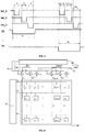
FIG. 3 is a control signal time sequence diagram of the data drive circuits shown inFIG. 2 andFIG. 6 ; -
FIG. 4 shows another data drive circuit of an organic light emitting display apparatus in prior art; -
FIG. 5 is a control signal time sequence diagram of the data drive circuits shown inFIG. 4 andFIG. 7 ; -
FIG. 6 shows a data drive circuit described inembodiment 1 of the present invention; -
FIG. 7 shows a data drive circuit described inembodiment 2 of the present invention. - In order to make the objective, technical scheme and advantages of the present invention more clear, hereinafter, detailed description of implementation ways of the embodiments of the present invention is given below, with reference to the appended drawings.
- Specific illustrative embodiments in accordance with the present invention are described below with reference to the appended drawings. Herein, when a first unit is described to be "connected" to a second unit, the first unit may be directly connected to the second unit, or may be indirectly connected to the second unit via one or more additional units. Furthermore, for the sake of clarity, some elements that are not necessary for fully understanding the present invention are omitted. Also, the same reference sign always refers to the same unit.
- This embodiment provides a data drive circuit, as shown in
FIG. 6 , the data drive circuit is electrically connected to adata driver 20 via m/i columns of data lines D1 ... D(m/2), and electrically connected to ascan driver 30 via n rows of scan lines S1, S2 ... Sn. In this embodiment, i has a value of 2. - The first column of data line D1 has an end away from the
data driver 20 that is connected to a first column of signal line D1' and a second column of signal line D2', likewise, the number j column of data line Dj has an end away from thedata driver 20 that is connected to a number 2j-1 column of signal line D(2j-1)' and a number 2j column of signal line D(2j)', j=1,2,3 ... m/2; the number m/2 column of data line D(m/2) has an end away from thedata driver 20 that is connected to two signal lines of a number m-1 column of signal line D(m-1)' and a number m column of signal line Dm'. The data drive circuit also comprisespixel units display area 40. In this embodiment, there are n rows, m columns of the pixel units arranged in thedisplay area 40, each row of the scan lines S1, S2 ... Sn is electrically connected to a corresponding row of pixel units arranged in thedisplay area 40, each column of the signal lines D1', D2' ... D(m-1)', Dm' is electrically connected to a corresponding column of pixel units arranged in thedisplay area 40, that is to say, a number m column of signal line Dm' and a number n row of scan line Sn are connected to a pixel unit nm at Row n Column m. - A first transistor T1, T2 ... T(m-1), Tm is respectively connected in a segment within each of the signal lines D1', D2' ... D(m-1)', Dm' between each of the data lines D1 ... D(m/2) and the
display area 40, said data drive circuit further comprises 2 rows of control lines Sel_1, Sel_2 connected to thedata driver 20. These first transistors T1, T2 ... T(m-1), Tm are preferably P-type transistors. - The gate electrodes of the two first transistors T1, T2 connected to the first column of data line D1 are respectively electrically connected to different lines Sel_1, Sel_2 of the control lines;
likewise, the gate electrodes of the two first transistors T(2j-1), T(2j) connected to the same data line Dj are respectively electrically connected to different lines Sel_1, Sel_2 of the control lines, j=1,2,3 ... m/2;
the gate electrodes of the two first transistors T(m-1), Tm connected to the number m/2 column of data line D(m/2) are respectively electrically connected to different lines Sel_1, Sel_2 of the control lines. - The data drive circuit further comprises a
power source line 50 and m/2 second transistors T2' ... Tm' connected to thepower source line 50, thepower source line 50 is connected to a power source Vref. The power source Vref has a voltage value lower than or equal to 0V, and preferable has a voltage of 0V in this embodiment. - The respective second transistors T2' ... Tm' have source electrodes all electrically connected to the
power source line 50, and gate electrodes electrically connected to the same line Sel_1 of the control lines. The drain electrode of the number j column of second transistor Tj' is electrically connected to the number j column of signal line Dj' at a connection point between the number j column of first transistor Tj and thedisplay area 40, j=2,4,6 ... m. That is to say, for example, the second column of second transistor T2' has a source electrode electrically connected to thepower source line 50, and a drain electrode connected to the second column of signal line D2' at a connection point between the second column of first transistor T2 and thedisplay area 40. - The first transistor T2, T4 ... T(m-2), Tm and the second transistor T2', T4' ... T(m-2)', Tm' connected to the same signal line D2', D4' ... D(m-2)', Dm' have their gate electrodes connected to different lines of the control lines, which are Sel_1, Sel_2 in this embodiment. Specifically, in this embodiment, the gate electrode of the second column of second transistor T2' is electrically connected to the control line Sel_1, while the gate electrode of the first transistor T2 in the same column is electrically connected to the control line Sel_2; ...the gate electrode of the number m column of second transistor Tm' is electrically connected to the control line Sel_1, while the gate electrode of the first transistor Tm in the same column is electrically connected to the control line Sel_2.
- All of the second transistors T2' ... Tm' are field effect transistors with the same channel polarity, and are preferably P-type field effect transistors in this embodiment.
- In other embodiments of the present invention, there can be m/i columns of data lines with i columns of signal lines connected to each column of data line, i rows of control lines, and m(i-1)/i second transistors, namely m-m/i second transistors, wherein i is a natural number larger than or equal to 2, m is a non-zero natural number that is an integer multiple of i. These other embodiments can all achieve the purpose of the present invention, and are embraced in the protection scope of the present invention.
- The drive method for the above-mentioned data drive circuit is that, dividing the data signal write cycle (Tj, j=1,2,3 ... n) of each column of data line into i time periods, preferably 2 time periods (t1, t2) in this embodiment. Taking the second row of pixel units as example, as shown in
FIG. 3 : - In a data signal write cycle T1 of the first column of data line D1, the first column of data line D1 transmits high level.
- Within the time period t1, the control line Sel_1 has low level, the control line Sel_2 has high level, the first column of first transistor T1 and the second column of second transistor T2' are switched on, while the second column of first transistor T2 is switched off; the high level on the first column of data line D1 is transmitted to the first column of signal line D1' in the
display area 40, and then the data signal on the signal line D1' is loaded onto the first column ofpixel units pixel units - Within the time period t2, the control line Sel_2 has low level, the control line Sel_1 has high level, the second column of first transistor T2 is switched on, while the first column of first transistor T1 and the second column of second transistor T2' are switched off; the high level on the first column of data line D1 is transmitted to the second column of signal line D2' in the
display area 40, and then the data signal on the signal line D2' is loaded onto the second column ofpixel units - In a data signal write cycle T2 of the second column of data line D2, the first column of data line D1 transmits low level.
- Within the time period t3, the control line Sel_1 has low level, the control line Sel_2 has high level, the first column of first transistor T1 and the second column of second transistor T2' are switched on, while the second column of first transistor T2 is switched off; the low level on the first column of data line D1 is transmitted to the first column of signal line D1' in the
display area 40, and the first column ofpixel units pixel units - Within the time period t4, the control line Sel_2 has low level, the control line Sel_1 has high level, the second column of first transistor T2 is switched on, while the first column of first transistor T1 and the second column of second transistor T2' are switched off; the first column of data line D1 transmits low level to the second column of signal line D2' in the
display area 40, and because the voltage on the second column ofpixel units pixel units - Therefore, the organic light emitting display apparatus equipped with this data drive circuit is not subjected to stray capacitance in the pixel units or from a signal line, and thus it can respond timely without ghost shadow, so as to display images normally.
- This embodiment provides a data drive circuit, as shown in
FIG. 7 , its particular circuit configuration is similar to that ofEmbodiment 1, and the only difference is that i is 3. That is to say, each column of data line has an end away from thedata driver 20 that is connected to 3 columns of signal lines, and there are 3 rows of control lines and 2m/3 second transistors, wherein m is a non-zero natural number that is an integer multiple of 3. - In particular, the first column of data line D1 has an end away from the
data driver 20 that is connected to a first column of signal line D1', a second column of signal line D2' and a third column of signal line D3', likewise, the number j column of data line Dj has an end away from thedata driver 20 that is connected to a number 3j-2 column of signal line D(3j-2)', a number 3j-1 column of signal line D(3j-1)' and a number 3j column of signal line D(3j'), j=1,2,3 ... m/3; the number m/3 column of data line D(m/3) has an end away from thedata driver 20 that is connected to three signal lines of a number m-2 column of signal line D(m-2)', a number m-1 column of signal line D(m-1)' and a number m column of signal line Dm'. - First transistors T1, T2 ... T(m-1), Tm are connected in a segment within the signal lines D1', D2' ... D(m-1)', Dm' between the data lines D1 ... D(m/3) and the
display area 40, said data drive circuit further comprises 3 rows of control lines Sel_1, Sel_2, Sel_3 connected to thedata driver 20. These first transistors T1, T2 ... T(m-1), Tm are preferably P-type transistors. - The gate electrodes of the three first transistors T1, T2, T3 connected to the first column of data line D1 are respectively electrically connected to different lines Sel_1, Sel_2, Sel_3 of the control lines;
likewise, the gate electrodes of the three first transistors T(3j-2), T(3j-1), T(3j) connected to the same data line Dj are respectively electrically connected to different lines Sel_1, Sel_2, Sel_3 of the control lines, j=1,2,3 ... m/3;
the gate electrodes of the three first transistors T(m-2), T(m-1), Tm connected to the number m/3 column of data line D(m/3) are respectively electrically connected to different lines Sel_1, Sel_2, Sel_3 of the control lines. - The data drive circuit further comprises a
power source line power source line 50, thepower source line 50 is connected to a power source Vref. The power source Vref has a voltage value lower than or equal to 0V, and preferable has a voltage of 0V in this embodiment. - That is to say, among the 3 signal lines connected to the end of each column of data line that is away from the
data driver 20, the latter two signal lines have a second transistor arranged between the respective signal line and thepower source line 50. For example, the data line D1 is connected to 3 signal lines D1', D2', D3', wherein the signal lines D2', D3' have a second transistor T2', T3' arranged between the respective signal line and thepower source line 50; and so on, the data line D(m/3) is connected to 3 signal lines D(m-2)', D(m-1)', Dm', wherein the signal lines D(m-1)', Dm' have a second transistor T(m-1)', Tm' arranged between the respective signal line and thepower source line 50. - In particular, the respective second transistors T2', T3' ...T(m-1)', Tm' have source electrodes all electrically connected to the
power source line 50, and gate electrodes electrically connected to the same line Sel_1 of the control lines. The drain electrode of the number j column of second transistor Tj' is electrically connected to the number j column of signal line Dj' at a connection point between the number j column of first transistor Tj and thedisplay area 40, j=2,3,5,6 ... m-1,m. That is to say, for example, the second column of second transistor T2' has a source electrode electrically connected to thepower source line 50, and a drain electrode connected to the second column of signal line D2' at a connection point between the second column of first transistor T2 and thedisplay area 40. - The first transistor T2, T3 ... T(m-1), Tm and the second transistor T2', T3' ...T(m-1)', Tm' connected to the same signal line D2', D3' ... D(m-1)', Dm' have their gate electrodes connected to different lines of the control lines.
- All of the second transistors T2' ... Tm' are field effect transistors with the same channel polarity, and are preferably P-type field effect transistors in this embodiment.
- In other embodiments of the present invention, there can be m/i columns of data lines with i columns of signal lines connected to each column of data line, i rows of control lines, and m(i-1)/i second transistors, namely m-m/i second transistors, wherein i is a natural number larger than or equal to 2, m is a non-zero natural number that is an integer multiple of i. These other embodiments can all achieve the purpose of the present invention, and are embraced in the protection scope of the present invention.
- The drive method for the above-mentioned data drive circuit is that, as shown in
FIG. 5 , dividing the data signal write cycle (Tj, j=1,2,3 ... n) of each column of data line into 3 time periods. - Within the time period t1, the control line Sel_1 has low level, the control lines Sel_2 and Sel_3 have high level, the first column of first transistor T1, the second column of second transistor T2' and the third column of second transistor T3' are switched on, while the second column of first transistor T2 and the third column of first transistor T3 are switched off;
the data signal on the first column of signal line D1' is loaded onto the first column ofpixel units pixel units pixel units - Within the time period t2, the control line Sel_2 has low level, the control lines Sel_1 and Sel_3 have high level, the second column of first transistor T2 is switched on, while the first column of first transistor T1, the second column of second transistor T2', the third column of first transistor T3 and the third column of second transistor T3' are switched off;
the electrical level on the first column of data line D1 is transmitted to the second column of signal line D2' in thedisplay area 40, and then the data signal on the signal line D2' is loaded onto the second column ofpixel units - Within the time period t3, the control line Sel_3 has low level, the control lines Sel_1 and Sel_2 have high level, the third column of first transistor T3 is switched on, while the first column of first transistor T1, the second column of first transistor T2, the second column of second transistor T2' and the third column of second transistor T3' are switched off; the data signal on the third column of signal line D3' is loaded onto the third column of
pixel units - Thereby, before the data signal write cycle of the next column of data line begins, the pixel units in the column corresponding to each column of signal line are initialized, so as not to be subjected to stray capacitance in the pixel units or from a signal line, and thus can respond timely without ghost shadow, thereby ensuring normal displaying.
- The present invention also provides an organic light emitting display that comprises the above-mentioned data drive circuit. Its specific configurations are not repeatedly described herein. This organic light emitting display is not subjected to stray capacitance in the pixel units or from a signal line, and thus can respond timely without ghost shadow.
- Apparently, the aforementioned embodiments are merely examples illustrated for clearly describing the present invention, rather than limiting the implementation ways thereof. For those skilled in the art, various changes and modifications in other different forms can be made on the basis of the aforementioned description. It is unnecessary and impossible to exhaustively list all the implementation ways herein. However, any obvious changes or modifications derived from the aforementioned description are intended to be embraced within the protection scope of the present invention.
Claims (10)
- A data drive circuit, electrically connected to a data driver via m/i columns of data lines, and electrically connected to a scan driver via n rows of scan lines, wherein,each data line is connected to i columns of signal lines at an end away from the data driver, each row of the scan lines is electrically connected to a corresponding row of pixel units arranged in a display area, each column of the signal lines is electrically connected to a corresponding column of pixel units arranged in the display area;a first transistor is connected in a segment within each signal line between the data line and the display area, said data drive circuit further comprises i rows of control lines connected to the data driver;the i first transistors connected to the same data line respectively have gate electrodes electrically connected to different lines of the control lines;i is a natural number larger than or equal to 2, m is a non-zero natural number that is an integer multiple of i, n is a non-zero natural number;characterized in that,said data drive circuit further comprises a power source line and m-m/i second transistors connected to the power source line, the power source line is connected to a power source;the respective second transistors have source electrodes all electrically connected to the power source line, gate electrodes electrically connected to the same line of the control lines, and drain electrodes respectively electrically connected to different lines of the signal lines at a connection point between the first transistor and the display area.
- The data drive circuit of Claim 1, characterized in that, the first transistor and second transistor connected to the same signal line have gate electrodes connected to different lines of the control lines.
- The data drive circuit of Claim 1, characterized in that, the power source has a voltage value lower than or equal to 0V.
- The data drive circuit of Claim 1, characterized in that, all of the first transistors are P-type transistors.
- The data drive circuit of any one of Claims 1-4, characterized in that, all of the second transistors are field effect transistors with the same channel polarity.
- The data drive circuit of Claim 5, characterized in that, the second transistors are P-type field effect transistors.
- A drive method for the data drive circuit of any one of Claims 1-6, characterized in that, dividing the data signal write cycle of each column of data line into i time periods; sequentially setting each of the control lines to be low level in each of the time periods;in the first of the time periods, the second transistor connected to the control line set at low level is switched on, so that the signal line connected to this second transistor is connected to the power source, and the pixel units in the column corresponding to this signal line is initialized.
- The drive method of Claim 7, characterized in that, in each of the time periods, the first transistor connected to the control line set at low level is switched on, so that the signal line connected to this first transistor is connected to the data line, and signal is written into the pixel units in the column corresponding to this signal line.
- The drive method of Claim 7, characterized in that, the voltage for the initialization is lower than or equal to 0V.
- An organic light emitting display, characterized in comprising the data drive circuit of any one of Claims 1-6.
Applications Claiming Priority (2)
| Application Number | Priority Date | Filing Date | Title |
|---|---|---|---|
| CN201410834484.XA CN105810143B (en) | 2014-12-29 | 2014-12-29 | A kind of data drive circuit and its driving method and organic light emitting display |
| PCT/CN2015/097996 WO2016107432A1 (en) | 2014-12-29 | 2015-12-21 | Data drive circuit and drive method therefor, and organic light emitting display |
Publications (2)
| Publication Number | Publication Date |
|---|---|
| EP3242288A1 true EP3242288A1 (en) | 2017-11-08 |
| EP3242288A4 EP3242288A4 (en) | 2018-06-13 |
Family
ID=56284222
Family Applications (1)
| Application Number | Title | Priority Date | Filing Date |
|---|---|---|---|
| EP15875110.7A Ceased EP3242288A4 (en) | 2014-12-29 | 2015-12-21 | Data drive circuit and drive method therefor, and organic light emitting display |
Country Status (7)
| Country | Link |
|---|---|
| US (1) | US20170372662A1 (en) |
| EP (1) | EP3242288A4 (en) |
| JP (1) | JP2018500606A (en) |
| KR (1) | KR20170100648A (en) |
| CN (1) | CN105810143B (en) |
| TW (1) | TWI570693B (en) |
| WO (1) | WO2016107432A1 (en) |
Families Citing this family (19)
| Publication number | Priority date | Publication date | Assignee | Title |
|---|---|---|---|---|
| CN108320704B (en) * | 2017-01-17 | 2020-12-25 | 上海和辉光电有限公司 | Display panel device |
| CN106940990B (en) * | 2017-04-24 | 2019-05-03 | 武汉华星光电技术有限公司 | Charging/discharging thereof and driving device, the display of display panel |
| JP6945877B2 (en) * | 2017-06-07 | 2021-10-06 | 深▲セン▼通鋭微電子技術有限公司 | Display device and image data correction method |
| TWI638216B (en) * | 2017-10-30 | 2018-10-11 | 友達光電股份有限公司 | Display device |
| KR102434029B1 (en) * | 2017-12-13 | 2022-08-18 | 엘지디스플레이 주식회사 | Display Device And Method Of Driving The Same |
| CN109785789B (en) * | 2018-04-18 | 2021-11-16 | 友达光电股份有限公司 | Multiplexer and display panel |
| CN110634451B (en) * | 2018-06-25 | 2023-04-11 | 矽创电子股份有限公司 | Driving method and driving circuit thereof |
| CN108986763A (en) * | 2018-09-20 | 2018-12-11 | 武汉华星光电半导体显示技术有限公司 | Display panel and its driving method |
| US10748466B2 (en) | 2018-09-20 | 2020-08-18 | Wuhan China Star Optoelectronics Semiconductor Display Technology Co., Ltd. | Display panel and method of driving the same |
| CN110189702B (en) * | 2019-06-28 | 2021-01-01 | 合肥视涯技术有限公司 | Organic light emitting display panel and driving method thereof |
| TWI706392B (en) * | 2019-07-25 | 2020-10-01 | 友達光電股份有限公司 | Display device and operating method thereof |
| US12217638B2 (en) * | 2021-07-02 | 2025-02-04 | Boe Technology Group Co., Ltd. | Display panel, display device, and method for driving display device |
| CN113889029B (en) * | 2021-09-29 | 2023-02-03 | 京东方科技集团股份有限公司 | A display panel, display device and data writing method |
| CN114120925B (en) * | 2021-11-29 | 2023-04-21 | 京东方科技集团股份有限公司 | Source electrode driving circuit and display device |
| CN114863873B (en) * | 2022-04-29 | 2023-07-21 | 武汉天马微电子有限公司 | Display panel and display device |
| CN114944138B (en) * | 2022-06-14 | 2023-07-25 | 合肥鑫晟光电科技有限公司 | Driving method, driving circuit and display device of display panel |
| CN115132127B (en) * | 2022-06-27 | 2025-07-25 | 京东方科技集团股份有限公司 | Display substrate and display device |
| CN116153251B (en) * | 2023-01-03 | 2024-07-05 | 武汉天马微电子有限公司 | Display panel, display panel driving method and display device |
| CN116704957A (en) * | 2023-06-27 | 2023-09-05 | 京东方科技集团股份有限公司 | A display substrate, its control method, and a display device |
Family Cites Families (20)
| Publication number | Priority date | Publication date | Assignee | Title |
|---|---|---|---|---|
| JP4191931B2 (en) * | 2001-09-04 | 2008-12-03 | 東芝松下ディスプレイテクノロジー株式会社 | Display device |
| KR100649243B1 (en) * | 2002-03-21 | 2006-11-24 | 삼성에스디아이 주식회사 | Organic electroluminescent display and driving method thereof |
| JP4610843B2 (en) * | 2002-06-20 | 2011-01-12 | カシオ計算機株式会社 | Display device and driving method of display device |
| TWI229313B (en) * | 2003-09-12 | 2005-03-11 | Au Optronics Corp | Display pixel circuit and driving method thereof |
| JP4203656B2 (en) * | 2004-01-16 | 2009-01-07 | カシオ計算機株式会社 | Display device and display panel driving method |
| JP2005331900A (en) * | 2004-06-30 | 2005-12-02 | Eastman Kodak Co | Display apparatus |
| US8199079B2 (en) * | 2004-08-25 | 2012-06-12 | Samsung Mobile Display Co., Ltd. | Demultiplexing circuit, light emitting display using the same, and driving method thereof |
| KR100602361B1 (en) * | 2004-09-22 | 2006-07-19 | 삼성에스디아이 주식회사 | Demultiplexer, light emitting display device using same and driving method thereof |
| KR100752289B1 (en) * | 2004-12-28 | 2007-08-29 | 세이코 엡슨 가부시키가이샤 | Unit circuit, method of controlling unit circuit, electronic device, and electronic apparatus |
| US8619007B2 (en) * | 2005-03-31 | 2013-12-31 | Lg Display Co., Ltd. | Electro-luminescence display device for implementing compact panel and driving method thereof |
| KR100796136B1 (en) * | 2006-09-13 | 2008-01-21 | 삼성에스디아이 주식회사 | Organic light emitting display device and driving method thereof |
| KR100897171B1 (en) * | 2007-07-27 | 2009-05-14 | 삼성모바일디스플레이주식회사 | Organic light emitting display |
| TWI373755B (en) * | 2007-10-30 | 2012-10-01 | Univ Nat Taiwan | Method for processing charging/discharging for updating data of array of pixels and circuit system for the same |
| JP2010281872A (en) * | 2009-06-02 | 2010-12-16 | Casio Computer Co Ltd | LIGHT EMITTING DEVICE, ITS DRIVE CONTROL METHOD, AND ELECTRONIC DEVICE |
| KR101082283B1 (en) * | 2009-09-02 | 2011-11-09 | 삼성모바일디스플레이주식회사 | Organic Light Emitting Display Device and Driving Method Thereof |
| TWI434258B (en) * | 2011-12-09 | 2014-04-11 | Au Optronics Corp | Data driving apparatus, corresponding operation method and corresponding display |
| KR102035718B1 (en) * | 2012-11-26 | 2019-10-24 | 삼성디스플레이 주식회사 | Organic Light Emitting Display Device and Driving Method Thereof |
| KR102055622B1 (en) * | 2013-01-10 | 2020-01-23 | 삼성디스플레이 주식회사 | Flat panel display device and method of driving a flat panel display device |
| KR102099311B1 (en) * | 2013-05-31 | 2020-04-10 | 삼성디스플레이 주식회사 | Display device |
| CN103927987B (en) * | 2014-04-02 | 2015-12-09 | 京东方科技集团股份有限公司 | Image element circuit and display device |
-
2014
- 2014-12-29 CN CN201410834484.XA patent/CN105810143B/en active Active
-
2015
- 2015-12-21 KR KR1020177021217A patent/KR20170100648A/en not_active Ceased
- 2015-12-21 EP EP15875110.7A patent/EP3242288A4/en not_active Ceased
- 2015-12-21 US US15/540,252 patent/US20170372662A1/en not_active Abandoned
- 2015-12-21 WO PCT/CN2015/097996 patent/WO2016107432A1/en not_active Ceased
- 2015-12-21 JP JP2017534769A patent/JP2018500606A/en active Pending
- 2015-12-28 TW TW104144033A patent/TWI570693B/en active
Also Published As
| Publication number | Publication date |
|---|---|
| TWI570693B (en) | 2017-02-11 |
| JP2018500606A (en) | 2018-01-11 |
| KR20170100648A (en) | 2017-09-04 |
| EP3242288A4 (en) | 2018-06-13 |
| CN105810143A (en) | 2016-07-27 |
| CN105810143B (en) | 2018-09-28 |
| WO2016107432A1 (en) | 2016-07-07 |
| TW201629939A (en) | 2016-08-16 |
| US20170372662A1 (en) | 2017-12-28 |
Similar Documents
| Publication | Publication Date | Title |
|---|---|---|
| US20170372662A1 (en) | Data drive circuit and drive method therefor, and organic light emitting display | |
| US20170061872A1 (en) | Pixel driving circuit, driving method for the same and display device | |
| CN104850270B (en) | Driving method, drive circuit, touch module, panel and the device of touch module | |
| US10290260B2 (en) | Pixel circuit having third drive circuit connected to first drive circuit and second drive circuit respectively, display panel and driving method | |
| US9262966B2 (en) | Pixel circuit, display panel and display apparatus | |
| US20170061890A1 (en) | Pixel driving circuit, driving method for display device | |
| US9984629B2 (en) | Pixel circuit and display device that sets a data line to a reference voltage to remove a residual data voltage | |
| EP2750123A1 (en) | Pixel circuit for organic light emitting display and driving method thereof, organic light emitting display | |
| EP3156994A1 (en) | Pixel driver circuit, driving method, array substrate, and display device | |
| CN109935210A (en) | Gate drivers and display device including the gate drivers | |
| US9437142B2 (en) | Pixel circuit and display apparatus | |
| CN105243996A (en) | AMOLED driving circuit structure adopting external compensation | |
| US20180329546A1 (en) | Touch display panel, a driving method thereof, and touch display device | |
| CN107833557B (en) | Displayer and its driving method | |
| US10235943B2 (en) | Display panel, method for controlling display panel and display device | |
| CN107092388A (en) | Touch control display apparatus and its driving method | |
| KR20160081241A (en) | Display device | |
| CN105448234A (en) | Pixel circuit, driving method thereof, and active matrix organic light emitting display | |
| CN102693696A (en) | Pixel circuit structure and method for driving pixel circuit structure | |
| CN103943066B (en) | A kind of image element circuit and driving method, display device | |
| CN206877300U (en) | Touch control display apparatus | |
| CN203760053U (en) | Pixel circuit and display device | |
| CN103988246A (en) | Double-sided display device and control method therefor | |
| US10621923B2 (en) | Scanning drive system of AMOLED display panel | |
| US10109235B2 (en) | Compensation circuit, AMOLED structure and display device |
Legal Events
| Date | Code | Title | Description |
|---|---|---|---|
| PUAI | Public reference made under article 153(3) epc to a published international application that has entered the european phase |
Free format text: ORIGINAL CODE: 0009012 |
|
| 17P | Request for examination filed |
Effective date: 20170704 |
|
| AK | Designated contracting states |
Kind code of ref document: A1 Designated state(s): AL AT BE BG CH CY CZ DE DK EE ES FI FR GB GR HR HU IE IS IT LI LT LU LV MC MK MT NL NO PL PT RO RS SE SI SK SM TR |
|
| AX | Request for extension of the european patent |
Extension state: BA ME |
|
| DAV | Request for validation of the european patent (deleted) | ||
| DAX | Request for extension of the european patent (deleted) | ||
| A4 | Supplementary search report drawn up and despatched |
Effective date: 20180516 |
|
| RIC1 | Information provided on ipc code assigned before grant |
Ipc: G09G 3/32 20160101AFI20180509BHEP |
|
| 17Q | First examination report despatched |
Effective date: 20190315 |
|
| REG | Reference to a national code |
Ref country code: DE Ref legal event code: R003 |
|
| STAA | Information on the status of an ep patent application or granted ep patent |
Free format text: STATUS: THE APPLICATION HAS BEEN REFUSED |
|
| 18R | Application refused |
Effective date: 20201212 |