EP3242074A1 - Lamp unit and vehicle lamp device using same - Google Patents
Lamp unit and vehicle lamp device using same Download PDFInfo
- Publication number
- EP3242074A1 EP3242074A1 EP15875664.3A EP15875664A EP3242074A1 EP 3242074 A1 EP3242074 A1 EP 3242074A1 EP 15875664 A EP15875664 A EP 15875664A EP 3242074 A1 EP3242074 A1 EP 3242074A1
- Authority
- EP
- European Patent Office
- Prior art keywords
- base assembly
- lamp unit
- protrusion
- lens
- contact
- Prior art date
- Legal status (The legal status is an assumption and is not a legal conclusion. Google has not performed a legal analysis and makes no representation as to the accuracy of the status listed.)
- Granted
Links
Images


Classifications
-
- F—MECHANICAL ENGINEERING; LIGHTING; HEATING; WEAPONS; BLASTING
- F21—LIGHTING
- F21S—NON-PORTABLE LIGHTING DEVICES; SYSTEMS THEREOF; VEHICLE LIGHTING DEVICES SPECIALLY ADAPTED FOR VEHICLE EXTERIORS
- F21S41/00—Illuminating devices specially adapted for vehicle exteriors, e.g. headlamps
- F21S41/20—Illuminating devices specially adapted for vehicle exteriors, e.g. headlamps characterised by refractors, transparent cover plates, light guides or filters
- F21S41/29—Attachment thereof
-
- F—MECHANICAL ENGINEERING; LIGHTING; HEATING; WEAPONS; BLASTING
- F21—LIGHTING
- F21S—NON-PORTABLE LIGHTING DEVICES; SYSTEMS THEREOF; VEHICLE LIGHTING DEVICES SPECIALLY ADAPTED FOR VEHICLE EXTERIORS
- F21S43/00—Signalling devices specially adapted for vehicle exteriors, e.g. brake lamps, direction indicator lights or reversing lights
- F21S43/10—Signalling devices specially adapted for vehicle exteriors, e.g. brake lamps, direction indicator lights or reversing lights characterised by the light source
- F21S43/13—Signalling devices specially adapted for vehicle exteriors, e.g. brake lamps, direction indicator lights or reversing lights characterised by the light source characterised by the type of light source
- F21S43/14—Light emitting diodes [LED]
-
- F—MECHANICAL ENGINEERING; LIGHTING; HEATING; WEAPONS; BLASTING
- F21—LIGHTING
- F21S—NON-PORTABLE LIGHTING DEVICES; SYSTEMS THEREOF; VEHICLE LIGHTING DEVICES SPECIALLY ADAPTED FOR VEHICLE EXTERIORS
- F21S43/00—Signalling devices specially adapted for vehicle exteriors, e.g. brake lamps, direction indicator lights or reversing lights
- F21S43/20—Signalling devices specially adapted for vehicle exteriors, e.g. brake lamps, direction indicator lights or reversing lights characterised by refractors, transparent cover plates, light guides or filters
- F21S43/26—Refractors, transparent cover plates, light guides or filters not provided in groups F21S43/235 - F21S43/255
-
- F—MECHANICAL ENGINEERING; LIGHTING; HEATING; WEAPONS; BLASTING
- F21—LIGHTING
- F21S—NON-PORTABLE LIGHTING DEVICES; SYSTEMS THEREOF; VEHICLE LIGHTING DEVICES SPECIALLY ADAPTED FOR VEHICLE EXTERIORS
- F21S43/00—Signalling devices specially adapted for vehicle exteriors, e.g. brake lamps, direction indicator lights or reversing lights
- F21S43/20—Signalling devices specially adapted for vehicle exteriors, e.g. brake lamps, direction indicator lights or reversing lights characterised by refractors, transparent cover plates, light guides or filters
- F21S43/27—Attachment thereof
-
- F—MECHANICAL ENGINEERING; LIGHTING; HEATING; WEAPONS; BLASTING
- F21—LIGHTING
- F21S—NON-PORTABLE LIGHTING DEVICES; SYSTEMS THEREOF; VEHICLE LIGHTING DEVICES SPECIALLY ADAPTED FOR VEHICLE EXTERIORS
- F21S45/00—Arrangements within vehicle lighting devices specially adapted for vehicle exteriors, for purposes other than emission or distribution of light
- F21S45/40—Cooling of lighting devices
- F21S45/47—Passive cooling, e.g. using fins, thermal conductive elements or openings
-
- F—MECHANICAL ENGINEERING; LIGHTING; HEATING; WEAPONS; BLASTING
- F21—LIGHTING
- F21V—FUNCTIONAL FEATURES OR DETAILS OF LIGHTING DEVICES OR SYSTEMS THEREOF; STRUCTURAL COMBINATIONS OF LIGHTING DEVICES WITH OTHER ARTICLES, NOT OTHERWISE PROVIDED FOR
- F21V17/00—Fastening of component parts of lighting devices, e.g. shades, globes, refractors, reflectors, filters, screens, grids or protective cages
- F21V17/06—Fastening of component parts of lighting devices, e.g. shades, globes, refractors, reflectors, filters, screens, grids or protective cages the fastening being onto or by the lampholder
-
- F—MECHANICAL ENGINEERING; LIGHTING; HEATING; WEAPONS; BLASTING
- F21—LIGHTING
- F21V—FUNCTIONAL FEATURES OR DETAILS OF LIGHTING DEVICES OR SYSTEMS THEREOF; STRUCTURAL COMBINATIONS OF LIGHTING DEVICES WITH OTHER ARTICLES, NOT OTHERWISE PROVIDED FOR
- F21V19/00—Fastening of light sources or lamp holders
- F21V19/001—Fastening of light sources or lamp holders the light sources being semiconductors devices, e.g. LEDs
-
- F—MECHANICAL ENGINEERING; LIGHTING; HEATING; WEAPONS; BLASTING
- F21—LIGHTING
- F21V—FUNCTIONAL FEATURES OR DETAILS OF LIGHTING DEVICES OR SYSTEMS THEREOF; STRUCTURAL COMBINATIONS OF LIGHTING DEVICES WITH OTHER ARTICLES, NOT OTHERWISE PROVIDED FOR
- F21V5/00—Refractors for light sources
- F21V5/04—Refractors for light sources of lens shape
-
- F—MECHANICAL ENGINEERING; LIGHTING; HEATING; WEAPONS; BLASTING
- F21—LIGHTING
- F21V—FUNCTIONAL FEATURES OR DETAILS OF LIGHTING DEVICES OR SYSTEMS THEREOF; STRUCTURAL COMBINATIONS OF LIGHTING DEVICES WITH OTHER ARTICLES, NOT OTHERWISE PROVIDED FOR
- F21V5/00—Refractors for light sources
- F21V5/04—Refractors for light sources of lens shape
- F21V5/048—Refractors for light sources of lens shape the lens being a simple lens adapted to cooperate with a point-like source for emitting mainly in one direction and having an axis coincident with the main light transmission direction, e.g. convergent or divergent lenses, plano-concave or plano-convex lenses
-
- G—PHYSICS
- G02—OPTICS
- G02B—OPTICAL ELEMENTS, SYSTEMS OR APPARATUS
- G02B19/00—Condensers, e.g. light collectors or similar non-imaging optics
- G02B19/0004—Condensers, e.g. light collectors or similar non-imaging optics characterised by the optical means employed
- G02B19/0009—Condensers, e.g. light collectors or similar non-imaging optics characterised by the optical means employed having refractive surfaces only
- G02B19/0014—Condensers, e.g. light collectors or similar non-imaging optics characterised by the optical means employed having refractive surfaces only at least one surface having optical power
-
- G—PHYSICS
- G02—OPTICS
- G02B—OPTICAL ELEMENTS, SYSTEMS OR APPARATUS
- G02B19/00—Condensers, e.g. light collectors or similar non-imaging optics
- G02B19/0033—Condensers, e.g. light collectors or similar non-imaging optics characterised by the use
- G02B19/0047—Condensers, e.g. light collectors or similar non-imaging optics characterised by the use for use with a light source
- G02B19/0061—Condensers, e.g. light collectors or similar non-imaging optics characterised by the use for use with a light source the light source comprising a LED
-
- F—MECHANICAL ENGINEERING; LIGHTING; HEATING; WEAPONS; BLASTING
- F21—LIGHTING
- F21V—FUNCTIONAL FEATURES OR DETAILS OF LIGHTING DEVICES OR SYSTEMS THEREOF; STRUCTURAL COMBINATIONS OF LIGHTING DEVICES WITH OTHER ARTICLES, NOT OTHERWISE PROVIDED FOR
- F21V17/00—Fastening of component parts of lighting devices, e.g. shades, globes, refractors, reflectors, filters, screens, grids or protective cages
- F21V17/10—Fastening of component parts of lighting devices, e.g. shades, globes, refractors, reflectors, filters, screens, grids or protective cages characterised by specific fastening means or way of fastening
- F21V17/16—Fastening of component parts of lighting devices, e.g. shades, globes, refractors, reflectors, filters, screens, grids or protective cages characterised by specific fastening means or way of fastening by deformation of parts; Snap action mounting
- F21V17/164—Fastening of component parts of lighting devices, e.g. shades, globes, refractors, reflectors, filters, screens, grids or protective cages characterised by specific fastening means or way of fastening by deformation of parts; Snap action mounting the parts being subjected to bending, e.g. snap joints
-
- F—MECHANICAL ENGINEERING; LIGHTING; HEATING; WEAPONS; BLASTING
- F21—LIGHTING
- F21V—FUNCTIONAL FEATURES OR DETAILS OF LIGHTING DEVICES OR SYSTEMS THEREOF; STRUCTURAL COMBINATIONS OF LIGHTING DEVICES WITH OTHER ARTICLES, NOT OTHERWISE PROVIDED FOR
- F21V3/00—Globes; Bowls; Cover glasses
-
- F—MECHANICAL ENGINEERING; LIGHTING; HEATING; WEAPONS; BLASTING
- F21—LIGHTING
- F21Y—INDEXING SCHEME ASSOCIATED WITH SUBCLASSES F21K, F21L, F21S and F21V, RELATING TO THE FORM OR THE KIND OF THE LIGHT SOURCES OR OF THE COLOUR OF THE LIGHT EMITTED
- F21Y2113/00—Combination of light sources
- F21Y2113/10—Combination of light sources of different colours
- F21Y2113/13—Combination of light sources of different colours comprising an assembly of point-like light sources
- F21Y2113/17—Combination of light sources of different colours comprising an assembly of point-like light sources forming a single encapsulated light source
-
- F—MECHANICAL ENGINEERING; LIGHTING; HEATING; WEAPONS; BLASTING
- F21—LIGHTING
- F21Y—INDEXING SCHEME ASSOCIATED WITH SUBCLASSES F21K, F21L, F21S and F21V, RELATING TO THE FORM OR THE KIND OF THE LIGHT SOURCES OR OF THE COLOUR OF THE LIGHT EMITTED
- F21Y2115/00—Light-generating elements of semiconductor light sources
- F21Y2115/10—Light-emitting diodes [LED]
Definitions
- the present invention relates to a lamp unit and a vehicle lamp device using the same, and more particularly, to a lamp unit in which a surface light source is formed and a vehicle lamp device using the same.
- a lamp is an apparatus configured to generate or adjust light for a specific purpose.
- An incandescent bulb, a fluorescent lamp, a neon lamp, or the like may be used as a light source of a lamp, and a light emitting diode (LED) has been recently used as the light source.
- LED light emitting diode
- LEDs are devices configured to change an electric signal into infrared rays or light using characteristics of a compound semiconductor, and do not use harmful materials such as mercury, and thus have fewer causes of environmental pollution unlike fluorescent lamps.
- a lifetime of an LED is longer than that of an incandescent bulb, a fluorescent lamp, or a neon lamp.
- the LED consumes low power and has excellent visibility due to a high color temperature and less glare when compared to the incandescent bulb, the fluorescent lamp, and the neon lamp.
- a lamp unit includes a light source module and a reflector configured to set a directional angle of light emitted from the light source module.
- the light source module may include at least one LED light source formed on a printed circuit board (PCB).
- the reflector may focus light emitted by an LED light source 1a to emit the light through an opening at a predetermined directional angle and may have a reflective surface at an inner side surface thereof.
- a lamp unit is a lamp configured to focus light emitted from a plurality of LED light sources to generate light, and a lamp in which an LED is used may be used for a backlight, a display device, an illumination lamp, a vehicle display lamp, a head lamp, or the like according to a use thereof.
- a lamp unit used in a vehicle is closely related to safe driving of the vehicle, it is very important for a driver of a vehicle adjacent to the driving vehicle to be able to clearly identify a light emitting state thereof.
- the lamp unit used in a vehicle has to secure a light quantity sufficient for a safe driving standard and secure an aesthetic function of an exterior of the vehicle.
- the present invention is directed to providing a lamp unit in which a surface light source can be realized with fewer light sources, and a vehicle lamp device using the same.
- the present invention is also directed to providing a lamp unit capable of being applied to a curved mounting object by a plurality of light sources being disposed on a flexible base plate, and a vehicle lamp device using the same.
- a lamp unit including an optical member, a base assembly disposed to be spaced a predetermined distance from the optical member with a space therebetween, a light source disposed on the base assembly, and a lens coupled to the base assembly to cover the light source, wherein the lens includes a first protrusion having a first contact surface in contact with one surface of the base assembly, and a second contact surface formed at a height different from that of the first contact surface to be in contact with the other surface of the base assembly and a second protrusion having a third contact surface disposed to be spaced apart from the first protrusion and configured to be in contact with the base assembly.
- the first protrusion may protrude from an edge of a lower surface of the lens toward the base assembly.
- the first contact surface may be in contact with an upper surface of the base assembly.
- the second contact surface may be in contact with a lower surface of the base assembly.
- the first contact surface may be formed as a stepped surface formed on the first protrusion and the second contact surface may be formed as a hooking surface of a hook formed on an end of the first protrusion.
- the first contact surface and the second contact surface may face the base assembly.
- the second contact surface may protrude from the end of the first protrusion in a radial direction of the lens.
- the second protrusion may protrude from an edge of a lower surface of the lens toward the base assembly.
- the third contact surface may be in contact with an upper surface of the base assembly.
- the third contact surface may be formed as a lower end surface of the second protrusion.
- the third contact surface may face the base assembly.
- An outermost side of the first protrusion may be continuous with an edge of a lower surface of the lens.
- An outermost side of the second protrusion may be continuous with an edge of the lower surface of the lens.
- At least two first protrusions identical to the first protrusion may be symmetrically disposed with respect to a center of the lens.
- At least two second protrusions identical to the second protrusion may be symmetrically disposed with respect to the center of the lens.
- a lower surface of the lens may be disposed to be spaced apart from an upper surface of the base assembly in a height direction thereof.
- a lower surface of the lens may be flat surface, and an upper surface of the lens may be a curved surface.
- the upper surface of the lens may include a groove corresponding to a center portion of a light emitting surface of the light source.
- a hole through which the first protrusion passes may be formed in the base assembly.
- the base assembly may include a heat sink and a substrate stacked on the heat sink.
- a first protrusion includes a first contact surface and a second contact surface configured to simultaneously grasp upper and lower surfaces of a base assembly, there is an advantageous effect in that a lens is prevented from being moved on or falling off of the substrate.
- a second protrusion is formed to be spaced apart from a first protrusion and includes a third contact surface configured to be in contact with a heat sink in a state in which the second protrusion passes through a substrate, there is an advantageous effect in that shaking of a lens on the substrate is prevented in a state in which the first protrusion fixes the lens.
- FIG. 1 is a view illustrating a lamp unit according to one exemplary embodiment of the present invention
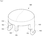
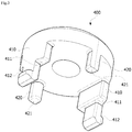
- FIGS. 2 and 3 are views illustrating a lens illustrated in FIG. 1
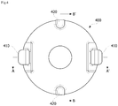
- FIG. 4 is a view illustrating a lower surface of a lens
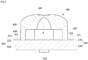
- FIG. 5 is a cross-sectional view taken along line A-A' of FIG. 4 and illustrates the lens mounted on a base assembly
- FIG. 6 is a cross-sectional view taken along line B-B' of FIG. 4 and illustrates the lens mounted on the base assembly.
- FIGS. 1 to 6 are views clearly illustrating main features for a clear conceptual understanding of the present invention, and thus various modifications are expected and the scope of the present invention is not limited to specific shapes illustrated in the drawings.
- the lamp unit may include an optical member 100, a base assembly 200, a light source 300, and a lens 400.
- the optical member 100 may be disposed to be spaced a predetermined distance from the base assembly 200 with a space therebetween, and a light mixing area may be formed in the space between the base assembly 200 the optical member 100.
- a surface light source may be formed with fewer light sources through light mixing.
- the optical member 100 may be disposed to be spaced about 10 mm or more from the base assembly 200.
- the lamp unit does not have uniform brightness and may have a hot spot phenomenon in which high brightness appears at an area at which the light source 300 is positioned, or a dark spot at which relatively low brightness appears may conversely appear.
- the optical member 100 is formed of at least one sheet and may selectively include a diffusion sheet, a prism sheet, a brightness enhancement sheet, and the like.
- the diffusion sheet diffuses light emitted by the light source 300
- the prism sheet guides the diffused light to a light emitting area
- the brightness enhancement sheet enhances brightness thereof.
- the diffusion sheet may be generally formed of an acrylic resin, but is not limited thereto.
- the diffusion sheet may be formed of a material such as polystyrene (PS), polymethyl methacrylate (PMMA), cyclic olefin copolymer (COC), polyethylene terephthalate (PET), a high permeability plastic such as a resin, or the like capable of performing a light diffusion function.
- the optical member 100 may have a concave-convex pattern on an upper surface thereof. This is to increase a diffusion effect thereof.
- the optical member 100 may have a surface having at least one among a concavely curved surface, a convexly curved surface, and a flat surface according to an outer shape of a cover member or a mounting object.
- the base assembly 200 may be formed to include a heat sink 210 and a substrate 220 stacked on the heat sink 210.
- the heat sink 210 serves to radiate heat generated by the light source 100 to the outside.
- the base assembly 200 may be a metal core printed circuit board (MCPCB) including the heat sink 210 and the substrate 220.
- MCPCB metal core printed circuit board
- the substrate 220 may selectively use a single layer PCB, a multilayer PCB, a ceramic substrate, an MCPCB, or the like.
- an entire portion of the substrate 220 may be made of the same material, or a part of the entire portion of the base assembly 200 may be made of different materials in some cases.
- the substrate 220 may include a supporting part which is in contact with the light source 300 and a connecting part which is not in contact with the light source 300 and, for example, the supporting part and the connecting part of the substrate 220 may be made of the same material.
- the supporting part and the connecting part may include circuit patterns, and a material of the substrate 220 may be a film having flexibility and insulation such as polyimide or epoxy (for example, FR-4).
- the supporting part and the connecting part of the substrate 220 may also be made of different materials.
- the supporting part may be a conductor, but the connecting part may be a nonconductor.
- the supporting part of the substrate 220 may be made of a hard material which does not bend to support the light source 100, but the connecting part of the substrate 220 may be made of a flexible material, and thus the base assembly 200 may also be manufactured to be applied to a curved mounting object.
- a circuit pattern for electrically connecting to the light source 100 is disposed on the circuit substrate 220, and a flexible and hard film may be disposed on one of upper and lower portions of the circuit pattern.
- the film may be one material selected from a photo solder resist (PSR), a polyimide, an epoxy (for example, FR-4), and the like or a combination thereof.
- the film disposed on the upper portion of the circuit pattern and the film disposed on the lower portion of the circuit pattern may be different.
- the substrate 220 may be bent by a flexible material being applied thereto, but may also be bent by changing a structure thereof.
- the light source 300 may be a top view type LED and may also be a side view type LED in some cases.
- the light source 100 may be an LED chip, and the LED chip may include a red LED chip, a blue LED chip, or an ultraviolet LED chip, or may include a package type including a combination of at least one or more of a red LED chip, a green LED chip, a blue LED chip, a yellow-green LED chip, and a white LED.
- the white LED may be realized by a blue LED coated with a yellow phosphor, by a blue LED simultaneously coated with a red phosphor and a green phosphor, or by a blue LED simultaneously coated with a yellow phosphor, a red phosphor, and a green phosphor.
- the light source 100 may be a vertical-type light emitting chip, for example, a red light emitting chip, but the embodiment is not limited thereto.
- the lens 400 may cover the light source 300 and may be coupled to the base assembly 200. At this time, the lens 400 may include first protrusions 410 and second protrusions 420.
- the first protrusion 410 may be formed to protrude from an edge of a lower surface 430 of the lens 400 toward the base assembly 200. Two first protrusions 410 may be symmetrically disposed with respect to the center of the lens 400. Such a first protrusion 410 may include a first contact surface 411 and a second contact surface 412.
- the first contact surface 411 is in contact with an upper surface of the base assembly 200 and serves to prevent the first protrusion 410 from being moved on the substrate 220.
- the first contact surface 411 may be formed as a stepped surface formed at a center portion of the first protrusion 410 and may be in contact with an upper surface of the heat sink 210 to face the base assembly 200. Accordingly, downward movement of the lens 400 due to an external force applied from an upper side of the lens 400 is prevented.
- the second contact surface 412 is in contact with a lower surface of the base assembly 200 and serves to prevent the first protrusion 410 from falling off of the substrate 220.
- the second contact surface 412 may be formed with a hooking surface of a hook formed on an end of the first protrusion 410. That is, the second contact surface 412 may be formed to protrude from the end of the first protrusion 410 in a radial direction of the lens 400. Such a second contact surface 412 may be in contact with a lower surface of the heat sink 210 to face the base assembly 200.
- the second contact surface 412 prevents the lens 400 from falling off of the substrate 220 due to an external force which pulls the lens 400 from above, or an external force or vibrations which push the lens 400 from below.
- the first protrusion 410 simultaneously grasps the upper and lower surfaces of the base assembly 200 using the first contact surface 411 and the second contact surface 412, a coupling property between the lens 400 and the base assembly 200 is improved.
- first holes 221 through which the first protrusions 410 pass may be formed in the substrate 220, and second holes 330 aligned with the first holes 221 may be formed in the heat sink 210 so that the first protrusions 410 pass therethrough.
- the second protrusion 420 may protrude toward the base assembly 200 from an edge of the lower surface 430 of the lens 400.
- the second protrusion 420 is disposed to be spaced a predetermined distance from the first protrusion 410, and two second protrusions 420 may be symmetrically disposed with respect to the center of the lens 400.
- Such a second protrusion 420 may include a third contact surface 421.
- the third contact surface 421 is in contact with the upper surface of the base assembly 200 and serves to prevent shaking of the lens 400 on the substrate 220.
- the third contact surface 421 may be formed as a lower end surface of the second protrusion 420, pass through the first hole 221 to face the base assembly 200, and be in contact with the upper surface of the heat sink 210. Accordingly, the third contact surface 421 serves to prevent the lens 400 from being shaken or moved due to vibrations in a state in which the lens 400 is primarily fixed by the first protrusion 410.
- the lower surface 430 of the lens 400 may be disposed to be spaced apart from the upper surface of the base assembly 200 in a height direction thereof.
- the lower surface 430 of the lens 400 may be a flat surface, and an upper surface of the lens 400 may be a curved surface.
- the lower surface 430 of the lens may be formed to include a groove corresponding to a center portion of a light emitting surface of the light source 300.
Landscapes
- Engineering & Computer Science (AREA)
- General Engineering & Computer Science (AREA)
- Physics & Mathematics (AREA)
- Optics & Photonics (AREA)
- General Physics & Mathematics (AREA)
- Microelectronics & Electronic Packaging (AREA)
- Non-Portable Lighting Devices Or Systems Thereof (AREA)
- Fastening Of Light Sources Or Lamp Holders (AREA)
- Lenses (AREA)
- Securing Globes, Refractors, Reflectors Or The Like (AREA)
- Planar Illumination Modules (AREA)
- Led Device Packages (AREA)
- Supplying Of Containers To The Packaging Station (AREA)
- Vehicle Body Suspensions (AREA)
- Arrangement Of Elements, Cooling, Sealing, Or The Like Of Lighting Devices (AREA)
Abstract
Description
- The present invention relates to a lamp unit and a vehicle lamp device using the same, and more particularly, to a lamp unit in which a surface light source is formed and a vehicle lamp device using the same.
- Generally, a lamp is an apparatus configured to generate or adjust light for a specific purpose.
- An incandescent bulb, a fluorescent lamp, a neon lamp, or the like may be used as a light source of a lamp, and a light emitting diode (LED) has been recently used as the light source.
- LEDs are devices configured to change an electric signal into infrared rays or light using characteristics of a compound semiconductor, and do not use harmful materials such as mercury, and thus have fewer causes of environmental pollution unlike fluorescent lamps.
- In addition, a lifetime of an LED is longer than that of an incandescent bulb, a fluorescent lamp, or a neon lamp. In addition, there are advantages in that the LED consumes low power and has excellent visibility due to a high color temperature and less glare when compared to the incandescent bulb, the fluorescent lamp, and the neon lamp.
- A lamp unit includes a light source module and a reflector configured to set a directional angle of light emitted from the light source module. Here, the light source module may include at least one LED light source formed on a printed circuit board (PCB).
- In addition, the reflector may focus light emitted by an LED light source 1a to emit the light through an opening at a predetermined directional angle and may have a reflective surface at an inner side surface thereof. Such a lamp unit is a lamp configured to focus light emitted from a plurality of LED light sources to generate light, and a lamp in which an LED is used may be used for a backlight, a display device, an illumination lamp, a vehicle display lamp, a head lamp, or the like according to a use thereof.
- Particularly, since a lamp unit used in a vehicle is closely related to safe driving of the vehicle, it is very important for a driver of a vehicle adjacent to the driving vehicle to be able to clearly identify a light emitting state thereof.
- Accordingly, the lamp unit used in a vehicle has to secure a light quantity sufficient for a safe driving standard and secure an aesthetic function of an exterior of the vehicle.
- The present invention is directed to providing a lamp unit in which a surface light source can be realized with fewer light sources, and a vehicle lamp device using the same.
- In addition, the present invention is also directed to providing a lamp unit capable of being applied to a curved mounting object by a plurality of light sources being disposed on a flexible base plate, and a vehicle lamp device using the same.
- The scope of the present invention is not limited to the above-described objects, and other unmentioned objects may be clearly understood by those skilled in the art from the following descriptions.
- According to an aspect of the present invention, there is provide a lamp unit including an optical member, a base assembly disposed to be spaced a predetermined distance from the optical member with a space therebetween, a light source disposed on the base assembly, and a lens coupled to the base assembly to cover the light source, wherein the lens includes a first protrusion having a first contact surface in contact with one surface of the base assembly, and a second contact surface formed at a height different from that of the first contact surface to be in contact with the other surface of the base assembly and a second protrusion having a third contact surface disposed to be spaced apart from the first protrusion and configured to be in contact with the base assembly.
- The first protrusion may protrude from an edge of a lower surface of the lens toward the base assembly.
- The first contact surface may be in contact with an upper surface of the base assembly.
- The second contact surface may be in contact with a lower surface of the base assembly.
- The first contact surface may be formed as a stepped surface formed on the first protrusion and the second contact surface may be formed as a hooking surface of a hook formed on an end of the first protrusion.
- The first contact surface and the second contact surface may face the base assembly.
- The second contact surface may protrude from the end of the first protrusion in a radial direction of the lens.
- The second protrusion may protrude from an edge of a lower surface of the lens toward the base assembly.
- The third contact surface may be in contact with an upper surface of the base assembly.
- The third contact surface may be formed as a lower end surface of the second protrusion.
- The third contact surface may face the base assembly.
- An outermost side of the first protrusion may be continuous with an edge of a lower surface of the lens.
- An outermost side of the second protrusion may be continuous with an edge of the lower surface of the lens.
- At least two first protrusions identical to the first protrusion may be symmetrically disposed with respect to a center of the lens.
- At least two second protrusions identical to the second protrusion may be symmetrically disposed with respect to the center of the lens.
- A lower surface of the lens may be disposed to be spaced apart from an upper surface of the base assembly in a height direction thereof.
- A lower surface of the lens may be flat surface, and an upper surface of the lens may be a curved surface.
- The upper surface of the lens may include a groove corresponding to a center portion of a light emitting surface of the light source.
- A hole through which the first protrusion passes may be formed in the base assembly.
- The base assembly may include a heat sink and a substrate stacked on the heat sink.
- According to another aspect of the present invention, there is provided a vehicle lamp device using the above-described lamp unit.
- According to one embodiment of the present invention, since a first protrusion includes a first contact surface and a second contact surface configured to simultaneously grasp upper and lower surfaces of a base assembly, there is an advantageous effect in that a lens is prevented from being moved on or falling off of the substrate.
- In addition, according to one embodiment of the present invention, since a second protrusion is formed to be spaced apart from a first protrusion and includes a third contact surface configured to be in contact with a heat sink in a state in which the second protrusion passes through a substrate, there is an advantageous effect in that shaking of a lens on the substrate is prevented in a state in which the first protrusion fixes the lens.
-
-
FIG. 1 is a view illustrating a lamp unit according to one exemplary embodiment of the present invention. -
FIGS. 2 and3 are views illustrating a lens illustrated inFIG. 1 . -
FIG. 4 is a view illustrating a lower surface of a lens. -
FIG. 5 is a cross-sectional view taken along line A-A' ofFIG. 4 and illustrates the lens mounted on a base assembly. -
FIG. 6 is a cross-sectional view taken along line B-B' ofFIG. 4 and illustrates the lens mounted on the base assembly. - Hereinafter, an exemplary embodiment of the present invention will be described in detail with reference to the accompanying drawings. Purposes, specific advantages, and novel features of the present invention will be made clear from exemplary embodiments and the following detailed description in connection with the accompanying drawings. Terms and words used in this specification and claims thereof are not to be interpreted as limited to commonly used meanings or meanings in dictionaries, and should be interpreted as having meanings and concepts which are consistent with the technological scope of the present invention based on the principle that the inventors have appropriately defined concepts of terms in order to describe the present invention in the best way. In the description of the present invention, when it is determined that detailed descriptions of related well-known functions unnecessarily obscure the gist of the present invention, the detailed descriptions will be omitted.
- It should be understood that, although the terms including ordinal numbers such as second, first, and the like may be used herein in reference to elements of the present invention, such elements are not to be construed as limited by these terms. These terms are only used to distinguish one element from another. For example, a second element could be termed a first element, and a first element could be termed a second element, without departing from the scope of the present invention.
-
FIG. 1 is a view illustrating a lamp unit according to one exemplary embodiment of the present invention, andFIGS. 2 and3 are views illustrating a lens illustrated inFIG. 1 . In addition,FIG. 4 is a view illustrating a lower surface of a lens,FIG. 5 is a cross-sectional view taken along line A-A' ofFIG. 4 and illustrates the lens mounted on a base assembly, andFIG. 6 is a cross-sectional view taken along line B-B' ofFIG. 4 and illustrates the lens mounted on the base assembly. -
FIGS. 1 to 6 are views clearly illustrating main features for a clear conceptual understanding of the present invention, and thus various modifications are expected and the scope of the present invention is not limited to specific shapes illustrated in the drawings. - Referring to
FIGS. 1 to 6 , the lamp unit according to one exemplary embodiment of the present invention may include anoptical member 100, abase assembly 200, alight source 300, and alens 400. - First, as illustrated in
FIG. 1 , theoptical member 100 may be disposed to be spaced a predetermined distance from thebase assembly 200 with a space therebetween, and a light mixing area may be formed in the space between thebase assembly 200 theoptical member 100. A surface light source may be formed with fewer light sources through light mixing. - Here, the
optical member 100 may be disposed to be spaced about 10 mm or more from thebase assembly 200. - When the distance between the
optical member 100 and thebase assembly 200 is about 10 mm or less, the lamp unit does not have uniform brightness and may have a hot spot phenomenon in which high brightness appears at an area at which thelight source 300 is positioned, or a dark spot at which relatively low brightness appears may conversely appear. - In addition, the
optical member 100 is formed of at least one sheet and may selectively include a diffusion sheet, a prism sheet, a brightness enhancement sheet, and the like. Here, the diffusion sheet diffuses light emitted by thelight source 300, the prism sheet guides the diffused light to a light emitting area, and the brightness enhancement sheet enhances brightness thereof. For example, the diffusion sheet may be generally formed of an acrylic resin, but is not limited thereto. In addition, the diffusion sheet may be formed of a material such as polystyrene (PS), polymethyl methacrylate (PMMA), cyclic olefin copolymer (COC), polyethylene terephthalate (PET), a high permeability plastic such as a resin, or the like capable of performing a light diffusion function. In addition, theoptical member 100 may have a concave-convex pattern on an upper surface thereof. This is to increase a diffusion effect thereof. - Meanwhile, the
optical member 100 may have a surface having at least one among a concavely curved surface, a convexly curved surface, and a flat surface according to an outer shape of a cover member or a mounting object. - The
base assembly 200 may be formed to include aheat sink 210 and asubstrate 220 stacked on theheat sink 210. - The
heat sink 210 serves to radiate heat generated by thelight source 100 to the outside. At this time, thebase assembly 200 may be a metal core printed circuit board (MCPCB) including theheat sink 210 and thesubstrate 220. - The
substrate 220 may selectively use a single layer PCB, a multilayer PCB, a ceramic substrate, an MCPCB, or the like. Here, an entire portion of thesubstrate 220 may be made of the same material, or a part of the entire portion of thebase assembly 200 may be made of different materials in some cases. - For example, the
substrate 220 may include a supporting part which is in contact with thelight source 300 and a connecting part which is not in contact with thelight source 300 and, for example, the supporting part and the connecting part of thesubstrate 220 may be made of the same material. Here, the supporting part and the connecting part may include circuit patterns, and a material of thesubstrate 220 may be a film having flexibility and insulation such as polyimide or epoxy (for example, FR-4). - In some cases, the supporting part and the connecting part of the
substrate 220 may also be made of different materials. For example, the supporting part may be a conductor, but the connecting part may be a nonconductor. In addition, the supporting part of thesubstrate 220 may be made of a hard material which does not bend to support thelight source 100, but the connecting part of thesubstrate 220 may be made of a flexible material, and thus thebase assembly 200 may also be manufactured to be applied to a curved mounting object. - In some cases, a circuit pattern for electrically connecting to the
light source 100 is disposed on thecircuit substrate 220, and a flexible and hard film may be disposed on one of upper and lower portions of the circuit pattern. For example, the film may be one material selected from a photo solder resist (PSR), a polyimide, an epoxy (for example, FR-4), and the like or a combination thereof. - In addition, when films are disposed on the upper and lower portions of the circuit pattern, the film disposed on the upper portion of the circuit pattern and the film disposed on the lower portion of the circuit pattern may be different. As described above, the
substrate 220 may be bent by a flexible material being applied thereto, but may also be bent by changing a structure thereof. - The
light source 300 may be a top view type LED and may also be a side view type LED in some cases. Here, thelight source 100 may be an LED chip, and the LED chip may include a red LED chip, a blue LED chip, or an ultraviolet LED chip, or may include a package type including a combination of at least one or more of a red LED chip, a green LED chip, a blue LED chip, a yellow-green LED chip, and a white LED. - In addition, the white LED may be realized by a blue LED coated with a yellow phosphor, by a blue LED simultaneously coated with a red phosphor and a green phosphor, or by a blue LED simultaneously coated with a yellow phosphor, a red phosphor, and a green phosphor.
- For example, when the lamp unit is applied as a rear light of a vehicle, the
light source 100 may be a vertical-type light emitting chip, for example, a red light emitting chip, but the embodiment is not limited thereto. - The
lens 400 may cover thelight source 300 and may be coupled to thebase assembly 200. At this time, thelens 400 may includefirst protrusions 410 andsecond protrusions 420. - The
first protrusion 410 may be formed to protrude from an edge of alower surface 430 of thelens 400 toward thebase assembly 200. Twofirst protrusions 410 may be symmetrically disposed with respect to the center of thelens 400. Such afirst protrusion 410 may include afirst contact surface 411 and asecond contact surface 412. - The
first contact surface 411 is in contact with an upper surface of thebase assembly 200 and serves to prevent thefirst protrusion 410 from being moved on thesubstrate 220. Specifically, as illustrated inFIG. 5 , thefirst contact surface 411 may be formed as a stepped surface formed at a center portion of thefirst protrusion 410 and may be in contact with an upper surface of theheat sink 210 to face thebase assembly 200. Accordingly, downward movement of thelens 400 due to an external force applied from an upper side of thelens 400 is prevented. - The
second contact surface 412 is in contact with a lower surface of thebase assembly 200 and serves to prevent thefirst protrusion 410 from falling off of thesubstrate 220. Specifically, as illustrated inFIG. 5 , thesecond contact surface 412 may be formed with a hooking surface of a hook formed on an end of thefirst protrusion 410. That is, thesecond contact surface 412 may be formed to protrude from the end of thefirst protrusion 410 in a radial direction of thelens 400. Such asecond contact surface 412 may be in contact with a lower surface of theheat sink 210 to face thebase assembly 200. - Accordingly, the
second contact surface 412 prevents thelens 400 from falling off of thesubstrate 220 due to an external force which pulls thelens 400 from above, or an external force or vibrations which push thelens 400 from below. - As described above, since the
first protrusion 410 simultaneously grasps the upper and lower surfaces of thebase assembly 200 using thefirst contact surface 411 and thesecond contact surface 412, a coupling property between thelens 400 and thebase assembly 200 is improved. - Meanwhile, as illustrated in
FIG. 5 ,first holes 221 through which thefirst protrusions 410 pass may be formed in thesubstrate 220, andsecond holes 330 aligned with thefirst holes 221 may be formed in theheat sink 210 so that thefirst protrusions 410 pass therethrough. - The
second protrusion 420 may protrude toward thebase assembly 200 from an edge of thelower surface 430 of thelens 400. Thesecond protrusion 420 is disposed to be spaced a predetermined distance from thefirst protrusion 410, and twosecond protrusions 420 may be symmetrically disposed with respect to the center of thelens 400. Such asecond protrusion 420 may include athird contact surface 421. - The
third contact surface 421 is in contact with the upper surface of thebase assembly 200 and serves to prevent shaking of thelens 400 on thesubstrate 220. Specifically, as illustrated inFIG. 6 , thethird contact surface 421 may be formed as a lower end surface of thesecond protrusion 420, pass through thefirst hole 221 to face thebase assembly 200, and be in contact with the upper surface of theheat sink 210. Accordingly, thethird contact surface 421 serves to prevent thelens 400 from being shaken or moved due to vibrations in a state in which thelens 400 is primarily fixed by thefirst protrusion 410. - Meanwhile, the
lower surface 430 of thelens 400 may be disposed to be spaced apart from the upper surface of thebase assembly 200 in a height direction thereof. In addition, thelower surface 430 of thelens 400 may be a flat surface, and an upper surface of thelens 400 may be a curved surface. In addition, thelower surface 430 of the lens may be formed to include a groove corresponding to a center portion of a light emitting surface of thelight source 300. - The lamp unit and the vehicle lamp device using the lamp unit according to one exemplary embodiment of the present invention have been specifically described above with respect the accompanying drawings.
- While the present invention has been particularly described with reference to exemplary embodiments, those skilled in the art should understand that various changes in form and details may be made without departing from the spirit and scope of the present invention. Therefore, the exemplary embodiments should be considered in a descriptive sense only and not for purposes of limitation. The scope of the present invention is defined not by the detailed description of the present invention but by the appended claims, and encompasses all modifications and equivalents that fall within the scope of the appended claims.
[Reference Numerals] 100: OPTICAL MEMBER 200: BASE ASSEMBLY 210: HEAT SINK 220: SUBSTRATE 300: LIGHT SOURCE 400: LENS 410: FIRST PROTRUSION 411: FIRST CONTACT SURFACE 412: SECOND CONTACT SURFACE 420: SECOND PROTRUSION 421: THIRD CONTACT SURFACE
Claims (21)
- A lamp unit comprising:an optical member;a base assembly disposed to be spaced a predetermined distance from the optical member with a space therebetween;a light source disposed on the base assembly; anda lens coupled to the base assembly to cover the light source,wherein the lens includes a first protrusion having a first contact surface in contact with one surface of the base assembly and a second contact surface formed at a height different from that of the first contact surface to be in contact with the other surface of the base assembly, and a second protrusion having a third contact surface disposed to be spaced apart from the first protrusion and configured to be in contact with the base assembly.
- The lamp unit of claim 1, wherein the first protrusion protrudes from an edge of a lower surface of the lens toward the base assembly.
- The lamp unit of claim 1, wherein the first contact surface is in contact with an upper surface of the base assembly.
- The lamp unit of claim 3, wherein the second contact surface is in contact with a lower surface of the base assembly.
- The lamp unit of claim 4, wherein:the first contact surface is formed as a stepped surface formed on the first protrusion; andthe second contact surface is formed as a hooking surface of a hook formed on an end of the first protrusion.
- The lamp unit of claim 5, wherein the first contact surface and the second contact surface face the base assembly.
- The lamp unit of claim 6, wherein the second contact surface protrudes from the end of the first protrusion in a radial direction of the lens.
- The lamp unit of claim 1, wherein the second protrusion protrudes from an edge of a lower surface of the lens toward the base assembly.
- The lamp unit of claim 1, wherein the third contact surface is in contact with an upper surface of the base assembly.
- The lamp unit of claim 9, wherein the third contact surface is formed as a lower end surface of the second protrusion.
- The lamp unit of claim 1, wherein the third contact surface faces the base assembly.
- The lamp unit of claim 1, wherein an outermost side of the first protrusion is continuous with an edge of a lower surface of the lens.
- The lamp unit of claim 12, wherein an outermost side of the second protrusion is continuous with an edge of the lower surface of the lens.
- The lamp unit of claim 1, wherein at least two first protrusions identical to the first protrusion are symmetrically disposed with respect to a center of the lens.
- The lamp unit of claim 14, wherein at least two second protrusions identical to the second protrusion are symmetrically disposed with respect to the center of the lens.
- The lamp unit of claim 1, wherein a lower surface of the lens is disposed to be spaced apart from an upper surface of the base assembly in a height direction thereof.
- The lamp unit of claim 1, wherein:a lower surface of the lens is a flat surface; andan upper surface of the lens is a curved surface.
- The lamp unit of claim 17, wherein the upper surface of the lens includes a groove corresponding to a center portion of a light emitting surface of the light source.
- The lamp unit of claim 1, wherein a hole through which the first protrusion passes is formed in the base assembly.
- The lamp unit of claim 1, wherein the base assembly includes a heat sink and a substrate stacked on the heat sink.
- A vehicle lamp device which uses the lamp unit of any one of claims 1 to 20.
Applications Claiming Priority (2)
| Application Number | Priority Date | Filing Date | Title |
|---|---|---|---|
| KR1020140192397A KR102423383B1 (en) | 2014-12-29 | 2014-12-29 | Lighting apparatus |
| PCT/KR2015/014396 WO2016108570A1 (en) | 2014-12-29 | 2015-12-29 | Lamp unit and vehicle lamp device using same |
Publications (3)
| Publication Number | Publication Date |
|---|---|
| EP3242074A1 true EP3242074A1 (en) | 2017-11-08 |
| EP3242074A4 EP3242074A4 (en) | 2018-09-12 |
| EP3242074B1 EP3242074B1 (en) | 2020-02-12 |
Family
ID=56284629
Family Applications (1)
| Application Number | Title | Priority Date | Filing Date |
|---|---|---|---|
| EP15875664.3A Active EP3242074B1 (en) | 2014-12-29 | 2015-12-29 | Lamp unit and vehicle lamp device using same |
Country Status (6)
| Country | Link |
|---|---|
| US (1) | US10260702B2 (en) |
| EP (1) | EP3242074B1 (en) |
| JP (1) | JP6725517B2 (en) |
| KR (1) | KR102423383B1 (en) |
| CN (1) | CN107208861A (en) |
| WO (1) | WO2016108570A1 (en) |
Families Citing this family (9)
| Publication number | Priority date | Publication date | Assignee | Title |
|---|---|---|---|---|
| ES2883643T3 (en) * | 2015-10-01 | 2021-12-09 | Emergency Tech Inc | Lighting element for a vehicle |
| WO2017152739A1 (en) * | 2016-03-07 | 2017-09-14 | 欧普照明股份有限公司 | Optical element, light source module and illumination device |
| JP2018181477A (en) * | 2017-04-06 | 2018-11-15 | スタンレー電気株式会社 | Light guide mounting structure |
| FR3071036B1 (en) * | 2017-09-12 | 2019-08-23 | Psa Automobiles Sa | OPTICAL MODULE FOR LIGHTING DEVICE AND / OR LIGHT SIGNALING DEVICE |
| KR102666833B1 (en) * | 2018-03-15 | 2024-05-20 | 서울반도체 주식회사 | Display apparatus, backlight unit, light emitting module and lens |
| EP4488986A3 (en) | 2018-03-15 | 2025-04-02 | Seoul Semiconductor Co., Ltd. | Light emitting module and lens |
| CN110030530A (en) * | 2019-04-19 | 2019-07-19 | 帝宝车灯制造(合肥)有限公司 | For weakening the device of car light center brightness |
| WO2022065030A1 (en) | 2020-09-24 | 2022-03-31 | 株式会社小糸製作所 | Vehicular lamp and vehicular lamp production method |
| CN220688808U (en) * | 2023-09-04 | 2024-03-29 | 漳州立达信光电子科技有限公司 | Screw-free PAR lamp |
Family Cites Families (17)
| Publication number | Priority date | Publication date | Assignee | Title |
|---|---|---|---|---|
| US6520669B1 (en) | 2000-06-19 | 2003-02-18 | Light Sciences Corporation | Flexible substrate mounted solid-state light sources for exterior vehicular lighting |
| GB0123815D0 (en) * | 2001-10-03 | 2001-11-21 | 3M Innovative Properties Co | Light-guide lights providing a substantially monochromatic beam |
| US20070230182A1 (en) * | 2006-03-28 | 2007-10-04 | Yun Tai | Led module |
| FR2901347B1 (en) * | 2006-05-22 | 2008-07-18 | Valeo Vision Sa | THERMAL DISSIPATING COMPONENT AND DIODE LIGHTING AND / OR SIGNALING DEVICE EQUIPPED WITH SUCH A COMPONENT |
| DE102007050893B4 (en) * | 2007-10-24 | 2011-06-01 | Continental Automotive Gmbh | Method for positioning and mounting a LED assembly and positioning body therefor |
| DE202007016530U1 (en) * | 2007-11-23 | 2008-02-07 | Reisen, Willy | Electric light |
| US20100067240A1 (en) * | 2008-09-16 | 2010-03-18 | John Selverian | Optical Cup For Lighting Module |
| DE102008061688C5 (en) | 2008-12-11 | 2016-12-29 | Automotive Lighting Reutlingen Gmbh | Attachment optics for a light source |
| US8083380B2 (en) * | 2009-04-17 | 2011-12-27 | Mig Technology Inc. | Integrated structure for optical refractor |
| KR101191398B1 (en) * | 2009-08-26 | 2012-10-15 | 에스엘 주식회사 | Lamp for vehicle |
| JP2011198473A (en) * | 2010-03-17 | 2011-10-06 | Igari Industry Co Ltd | Condensing optical element and device using the same |
| CN201661961U (en) * | 2010-03-24 | 2010-12-01 | 帝宝工业股份有限公司 | Vehicle LED lamp and lamp holder thereof |
| FR2970060B1 (en) * | 2010-11-08 | 2014-11-21 | Valeo Vision | DEVICE FOR LIGHTING AND / OR SIGNALING A MOTOR VEHICLE |
| JP5538307B2 (en) * | 2011-06-21 | 2014-07-02 | 本田技研工業株式会社 | Lamp body and vehicle lamp unit |
| DE112013003456T5 (en) * | 2012-03-05 | 2015-05-07 | Seoul Semiconductor Co., Ltd. | Illuminating lens for short-distance illumination |
| JP5964132B2 (en) * | 2012-05-23 | 2016-08-03 | 船井電機株式会社 | Display device |
| KR102024291B1 (en) * | 2012-12-18 | 2019-09-23 | 엘지이노텍 주식회사 | Lamp unit and vehicle lamp apparatus for using the same |
-
2014
- 2014-12-29 KR KR1020140192397A patent/KR102423383B1/en active Active
-
2015
- 2015-12-29 US US15/540,960 patent/US10260702B2/en active Active
- 2015-12-29 WO PCT/KR2015/014396 patent/WO2016108570A1/en not_active Ceased
- 2015-12-29 CN CN201580071816.6A patent/CN107208861A/en active Pending
- 2015-12-29 EP EP15875664.3A patent/EP3242074B1/en active Active
- 2015-12-29 JP JP2017535062A patent/JP6725517B2/en active Active
Also Published As
| Publication number | Publication date |
|---|---|
| JP6725517B2 (en) | 2020-07-22 |
| EP3242074A4 (en) | 2018-09-12 |
| US20170356628A1 (en) | 2017-12-14 |
| KR102423383B1 (en) | 2022-07-22 |
| US10260702B2 (en) | 2019-04-16 |
| CN107208861A (en) | 2017-09-26 |
| KR20160082835A (en) | 2016-07-11 |
| JP2018501623A (en) | 2018-01-18 |
| EP3242074B1 (en) | 2020-02-12 |
| WO2016108570A1 (en) | 2016-07-07 |
Similar Documents
| Publication | Publication Date | Title |
|---|---|---|
| EP3242074B1 (en) | Lamp unit and vehicle lamp device using same | |
| CN102130109B (en) | Light emitting device and light unit using the same | |
| US8847481B2 (en) | Lighting device comprising photoluminescent plate | |
| CN102484195B (en) | Light emitting device and light unit using the light emitting device | |
| EP2355194A2 (en) | Light emitting device package | |
| KR101655463B1 (en) | Light emitting device package and light unit having the same | |
| KR102804437B1 (en) | Lighting apparatus | |
| JP6956110B2 (en) | Lighting device | |
| KR20150075215A (en) | Led package for illumination | |
| EP2325557A1 (en) | Illumination device with heat dissipation structure | |
| CN105609624B (en) | Lens, light-emitting device package including lens, and lighting device including the package | |
| KR102400249B1 (en) | Light emitting module and display including the module | |
| US8333486B2 (en) | Illumination device with heat dissipation structure | |
| KR101315703B1 (en) | Lighting device | |
| EP2317209A1 (en) | Illumination device with heat dissipation structure | |
| KR102127448B1 (en) | Light Emitting Device package | |
| KR101997240B1 (en) | Lighting device | |
| KR101941513B1 (en) | Light Emitting module | |
| KR101977280B1 (en) | Light emtting device package | |
| KR102316037B1 (en) | Light emitting device | |
| KR102093344B1 (en) | Lighting device | |
| KR20120031807A (en) | Light emitting element array | |
| KR20150031699A (en) | Lighting device | |
| KR20110107638A (en) | Light emitting device package and lighting system | |
| KR20140097901A (en) | Light Emitting Device |
Legal Events
| Date | Code | Title | Description |
|---|---|---|---|
| STAA | Information on the status of an ep patent application or granted ep patent |
Free format text: STATUS: THE INTERNATIONAL PUBLICATION HAS BEEN MADE |
|
| PUAI | Public reference made under article 153(3) epc to a published international application that has entered the european phase |
Free format text: ORIGINAL CODE: 0009012 |
|
| STAA | Information on the status of an ep patent application or granted ep patent |
Free format text: STATUS: REQUEST FOR EXAMINATION WAS MADE |
|
| 17P | Request for examination filed |
Effective date: 20170629 |
|
| AK | Designated contracting states |
Kind code of ref document: A1 Designated state(s): AL AT BE BG CH CY CZ DE DK EE ES FI FR GB GR HR HU IE IS IT LI LT LU LV MC MK MT NL NO PL PT RO RS SE SI SK SM TR |
|
| AX | Request for extension of the european patent |
Extension state: BA ME |
|
| DAV | Request for validation of the european patent (deleted) | ||
| DAX | Request for extension of the european patent (deleted) | ||
| REG | Reference to a national code |
Ref country code: DE Ref legal event code: R079 Ref document number: 602015047093 Country of ref document: DE Free format text: PREVIOUS MAIN CLASS: F21S0008100000 Ipc: F21V0005040000 |
|
| A4 | Supplementary search report drawn up and despatched |
Effective date: 20180816 |
|
| RIC1 | Information provided on ipc code assigned before grant |
Ipc: F21S 43/14 20180101ALI20180809BHEP Ipc: F21V 17/16 20060101ALI20180809BHEP Ipc: F21S 43/27 20180101ALI20180809BHEP Ipc: F21V 5/04 20060101AFI20180809BHEP |
|
| GRAP | Despatch of communication of intention to grant a patent |
Free format text: ORIGINAL CODE: EPIDOSNIGR1 |
|
| STAA | Information on the status of an ep patent application or granted ep patent |
Free format text: STATUS: GRANT OF PATENT IS INTENDED |
|
| INTG | Intention to grant announced |
Effective date: 20190814 |
|
| GRAS | Grant fee paid |
Free format text: ORIGINAL CODE: EPIDOSNIGR3 |
|
| GRAA | (expected) grant |
Free format text: ORIGINAL CODE: 0009210 |
|
| STAA | Information on the status of an ep patent application or granted ep patent |
Free format text: STATUS: THE PATENT HAS BEEN GRANTED |
|
| AK | Designated contracting states |
Kind code of ref document: B1 Designated state(s): AL AT BE BG CH CY CZ DE DK EE ES FI FR GB GR HR HU IE IS IT LI LT LU LV MC MK MT NL NO PL PT RO RS SE SI SK SM TR |
|
| REG | Reference to a national code |
Ref country code: GB Ref legal event code: FG4D |
|
| REG | Reference to a national code |
Ref country code: CH Ref legal event code: EP |
|
| REG | Reference to a national code |
Ref country code: AT Ref legal event code: REF Ref document number: 1232575 Country of ref document: AT Kind code of ref document: T Effective date: 20200215 |
|
| REG | Reference to a national code |
Ref country code: DE Ref legal event code: R096 Ref document number: 602015047093 Country of ref document: DE |
|
| REG | Reference to a national code |
Ref country code: IE Ref legal event code: FG4D |
|
| REG | Reference to a national code |
Ref country code: NL Ref legal event code: FP |
|
| PG25 | Lapsed in a contracting state [announced via postgrant information from national office to epo] |
Ref country code: RS Free format text: LAPSE BECAUSE OF FAILURE TO SUBMIT A TRANSLATION OF THE DESCRIPTION OR TO PAY THE FEE WITHIN THE PRESCRIBED TIME-LIMIT Effective date: 20200212 Ref country code: NO Free format text: LAPSE BECAUSE OF FAILURE TO SUBMIT A TRANSLATION OF THE DESCRIPTION OR TO PAY THE FEE WITHIN THE PRESCRIBED TIME-LIMIT Effective date: 20200512 Ref country code: FI Free format text: LAPSE BECAUSE OF FAILURE TO SUBMIT A TRANSLATION OF THE DESCRIPTION OR TO PAY THE FEE WITHIN THE PRESCRIBED TIME-LIMIT Effective date: 20200212 |
|
| REG | Reference to a national code |
Ref country code: LT Ref legal event code: MG4D |
|
| PG25 | Lapsed in a contracting state [announced via postgrant information from national office to epo] |
Ref country code: BG Free format text: LAPSE BECAUSE OF FAILURE TO SUBMIT A TRANSLATION OF THE DESCRIPTION OR TO PAY THE FEE WITHIN THE PRESCRIBED TIME-LIMIT Effective date: 20200512 Ref country code: LV Free format text: LAPSE BECAUSE OF FAILURE TO SUBMIT A TRANSLATION OF THE DESCRIPTION OR TO PAY THE FEE WITHIN THE PRESCRIBED TIME-LIMIT Effective date: 20200212 Ref country code: IS Free format text: LAPSE BECAUSE OF FAILURE TO SUBMIT A TRANSLATION OF THE DESCRIPTION OR TO PAY THE FEE WITHIN THE PRESCRIBED TIME-LIMIT Effective date: 20200612 Ref country code: SE Free format text: LAPSE BECAUSE OF FAILURE TO SUBMIT A TRANSLATION OF THE DESCRIPTION OR TO PAY THE FEE WITHIN THE PRESCRIBED TIME-LIMIT Effective date: 20200212 Ref country code: HR Free format text: LAPSE BECAUSE OF FAILURE TO SUBMIT A TRANSLATION OF THE DESCRIPTION OR TO PAY THE FEE WITHIN THE PRESCRIBED TIME-LIMIT Effective date: 20200212 Ref country code: GR Free format text: LAPSE BECAUSE OF FAILURE TO SUBMIT A TRANSLATION OF THE DESCRIPTION OR TO PAY THE FEE WITHIN THE PRESCRIBED TIME-LIMIT Effective date: 20200513 |
|
| PG25 | Lapsed in a contracting state [announced via postgrant information from national office to epo] |
Ref country code: PT Free format text: LAPSE BECAUSE OF FAILURE TO SUBMIT A TRANSLATION OF THE DESCRIPTION OR TO PAY THE FEE WITHIN THE PRESCRIBED TIME-LIMIT Effective date: 20200705 Ref country code: SK Free format text: LAPSE BECAUSE OF FAILURE TO SUBMIT A TRANSLATION OF THE DESCRIPTION OR TO PAY THE FEE WITHIN THE PRESCRIBED TIME-LIMIT Effective date: 20200212 Ref country code: ES Free format text: LAPSE BECAUSE OF FAILURE TO SUBMIT A TRANSLATION OF THE DESCRIPTION OR TO PAY THE FEE WITHIN THE PRESCRIBED TIME-LIMIT Effective date: 20200212 Ref country code: CZ Free format text: LAPSE BECAUSE OF FAILURE TO SUBMIT A TRANSLATION OF THE DESCRIPTION OR TO PAY THE FEE WITHIN THE PRESCRIBED TIME-LIMIT Effective date: 20200212 Ref country code: RO Free format text: LAPSE BECAUSE OF FAILURE TO SUBMIT A TRANSLATION OF THE DESCRIPTION OR TO PAY THE FEE WITHIN THE PRESCRIBED TIME-LIMIT Effective date: 20200212 Ref country code: LT Free format text: LAPSE BECAUSE OF FAILURE TO SUBMIT A TRANSLATION OF THE DESCRIPTION OR TO PAY THE FEE WITHIN THE PRESCRIBED TIME-LIMIT Effective date: 20200212 Ref country code: DK Free format text: LAPSE BECAUSE OF FAILURE TO SUBMIT A TRANSLATION OF THE DESCRIPTION OR TO PAY THE FEE WITHIN THE PRESCRIBED TIME-LIMIT Effective date: 20200212 Ref country code: SM Free format text: LAPSE BECAUSE OF FAILURE TO SUBMIT A TRANSLATION OF THE DESCRIPTION OR TO PAY THE FEE WITHIN THE PRESCRIBED TIME-LIMIT Effective date: 20200212 Ref country code: EE Free format text: LAPSE BECAUSE OF FAILURE TO SUBMIT A TRANSLATION OF THE DESCRIPTION OR TO PAY THE FEE WITHIN THE PRESCRIBED TIME-LIMIT Effective date: 20200212 |
|
| REG | Reference to a national code |
Ref country code: DE Ref legal event code: R097 Ref document number: 602015047093 Country of ref document: DE |
|
| REG | Reference to a national code |
Ref country code: AT Ref legal event code: MK05 Ref document number: 1232575 Country of ref document: AT Kind code of ref document: T Effective date: 20200212 |
|
| PLBE | No opposition filed within time limit |
Free format text: ORIGINAL CODE: 0009261 |
|
| STAA | Information on the status of an ep patent application or granted ep patent |
Free format text: STATUS: NO OPPOSITION FILED WITHIN TIME LIMIT |
|
| 26N | No opposition filed |
Effective date: 20201113 |
|
| PG25 | Lapsed in a contracting state [announced via postgrant information from national office to epo] |
Ref country code: AT Free format text: LAPSE BECAUSE OF FAILURE TO SUBMIT A TRANSLATION OF THE DESCRIPTION OR TO PAY THE FEE WITHIN THE PRESCRIBED TIME-LIMIT Effective date: 20200212 Ref country code: IT Free format text: LAPSE BECAUSE OF FAILURE TO SUBMIT A TRANSLATION OF THE DESCRIPTION OR TO PAY THE FEE WITHIN THE PRESCRIBED TIME-LIMIT Effective date: 20200212 |
|
| PG25 | Lapsed in a contracting state [announced via postgrant information from national office to epo] |
Ref country code: PL Free format text: LAPSE BECAUSE OF FAILURE TO SUBMIT A TRANSLATION OF THE DESCRIPTION OR TO PAY THE FEE WITHIN THE PRESCRIBED TIME-LIMIT Effective date: 20200212 Ref country code: SI Free format text: LAPSE BECAUSE OF FAILURE TO SUBMIT A TRANSLATION OF THE DESCRIPTION OR TO PAY THE FEE WITHIN THE PRESCRIBED TIME-LIMIT Effective date: 20200212 |
|
| REG | Reference to a national code |
Ref country code: CH Ref legal event code: PL |
|
| PG25 | Lapsed in a contracting state [announced via postgrant information from national office to epo] |
Ref country code: MC Free format text: LAPSE BECAUSE OF FAILURE TO SUBMIT A TRANSLATION OF THE DESCRIPTION OR TO PAY THE FEE WITHIN THE PRESCRIBED TIME-LIMIT Effective date: 20200212 |
|
| REG | Reference to a national code |
Ref country code: BE Ref legal event code: MM Effective date: 20201231 |
|
| PG25 | Lapsed in a contracting state [announced via postgrant information from national office to epo] |
Ref country code: FR Free format text: LAPSE BECAUSE OF NON-PAYMENT OF DUE FEES Effective date: 20201231 Ref country code: LU Free format text: LAPSE BECAUSE OF NON-PAYMENT OF DUE FEES Effective date: 20201229 Ref country code: IE Free format text: LAPSE BECAUSE OF NON-PAYMENT OF DUE FEES Effective date: 20201229 |
|
| PG25 | Lapsed in a contracting state [announced via postgrant information from national office to epo] |
Ref country code: LI Free format text: LAPSE BECAUSE OF NON-PAYMENT OF DUE FEES Effective date: 20201231 Ref country code: CH Free format text: LAPSE BECAUSE OF NON-PAYMENT OF DUE FEES Effective date: 20201231 |
|
| PG25 | Lapsed in a contracting state [announced via postgrant information from national office to epo] |
Ref country code: TR Free format text: LAPSE BECAUSE OF FAILURE TO SUBMIT A TRANSLATION OF THE DESCRIPTION OR TO PAY THE FEE WITHIN THE PRESCRIBED TIME-LIMIT Effective date: 20200212 Ref country code: MT Free format text: LAPSE BECAUSE OF FAILURE TO SUBMIT A TRANSLATION OF THE DESCRIPTION OR TO PAY THE FEE WITHIN THE PRESCRIBED TIME-LIMIT Effective date: 20200212 Ref country code: CY Free format text: LAPSE BECAUSE OF FAILURE TO SUBMIT A TRANSLATION OF THE DESCRIPTION OR TO PAY THE FEE WITHIN THE PRESCRIBED TIME-LIMIT Effective date: 20200212 |
|
| PG25 | Lapsed in a contracting state [announced via postgrant information from national office to epo] |
Ref country code: MK Free format text: LAPSE BECAUSE OF FAILURE TO SUBMIT A TRANSLATION OF THE DESCRIPTION OR TO PAY THE FEE WITHIN THE PRESCRIBED TIME-LIMIT Effective date: 20200212 Ref country code: AL Free format text: LAPSE BECAUSE OF FAILURE TO SUBMIT A TRANSLATION OF THE DESCRIPTION OR TO PAY THE FEE WITHIN THE PRESCRIBED TIME-LIMIT Effective date: 20200212 |
|
| PG25 | Lapsed in a contracting state [announced via postgrant information from national office to epo] |
Ref country code: BE Free format text: LAPSE BECAUSE OF NON-PAYMENT OF DUE FEES Effective date: 20201231 |
|
| PGFP | Annual fee paid to national office [announced via postgrant information from national office to epo] |
Ref country code: NL Payment date: 20221122 Year of fee payment: 8 Ref country code: GB Payment date: 20221121 Year of fee payment: 8 Ref country code: DE Payment date: 20221121 Year of fee payment: 8 |
|
| REG | Reference to a national code |
Ref country code: DE Ref legal event code: R119 Ref document number: 602015047093 Country of ref document: DE |
|
| REG | Reference to a national code |
Ref country code: NL Ref legal event code: MM Effective date: 20240101 |
|
| GBPC | Gb: european patent ceased through non-payment of renewal fee |
Effective date: 20231229 |
|
| PG25 | Lapsed in a contracting state [announced via postgrant information from national office to epo] |
Ref country code: NL Free format text: LAPSE BECAUSE OF NON-PAYMENT OF DUE FEES Effective date: 20240101 |
|
| PG25 | Lapsed in a contracting state [announced via postgrant information from national office to epo] |
Ref country code: NL Free format text: LAPSE BECAUSE OF NON-PAYMENT OF DUE FEES Effective date: 20240101 |
|
| PG25 | Lapsed in a contracting state [announced via postgrant information from national office to epo] |
Ref country code: DE Free format text: LAPSE BECAUSE OF NON-PAYMENT OF DUE FEES Effective date: 20240702 |
|
| PG25 | Lapsed in a contracting state [announced via postgrant information from national office to epo] |
Ref country code: GB Free format text: LAPSE BECAUSE OF NON-PAYMENT OF DUE FEES Effective date: 20231229 |
|
| PG25 | Lapsed in a contracting state [announced via postgrant information from national office to epo] |
Ref country code: GB Free format text: LAPSE BECAUSE OF NON-PAYMENT OF DUE FEES Effective date: 20231229 Ref country code: DE Free format text: LAPSE BECAUSE OF NON-PAYMENT OF DUE FEES Effective date: 20240702 |