EP3240023A1 - Method and apparatus for semiconductor packaging - Google Patents
Method and apparatus for semiconductor packaging Download PDFInfo
- Publication number
- EP3240023A1 EP3240023A1 EP17167238.9A EP17167238A EP3240023A1 EP 3240023 A1 EP3240023 A1 EP 3240023A1 EP 17167238 A EP17167238 A EP 17167238A EP 3240023 A1 EP3240023 A1 EP 3240023A1
- Authority
- EP
- European Patent Office
- Prior art keywords
- passivation layer
- trenches
- layer
- pads
- die
- Prior art date
- Legal status (The legal status is an assumption and is not a legal conclusion. Google has not performed a legal analysis and makes no representation as to the accuracy of the status listed.)
- Withdrawn
Links
Images


Classifications
-
- H—ELECTRICITY
- H10—SEMICONDUCTOR DEVICES; ELECTRIC SOLID-STATE DEVICES NOT OTHERWISE PROVIDED FOR
- H10W—GENERIC PACKAGES, INTERCONNECTIONS, CONNECTORS OR OTHER CONSTRUCTIONAL DETAILS OF DEVICES COVERED BY CLASS H10
- H10W74/00—Encapsulations, e.g. protective coatings
- H10W74/10—Encapsulations, e.g. protective coatings characterised by their shape or disposition
- H10W74/131—Encapsulations, e.g. protective coatings characterised by their shape or disposition the semiconductor body being only partially enclosed
- H10W74/137—Encapsulations, e.g. protective coatings characterised by their shape or disposition the semiconductor body being only partially enclosed the encapsulations being directly on the semiconductor body
-
- H—ELECTRICITY
- H10—SEMICONDUCTOR DEVICES; ELECTRIC SOLID-STATE DEVICES NOT OTHERWISE PROVIDED FOR
- H10W—GENERIC PACKAGES, INTERCONNECTIONS, CONNECTORS OR OTHER CONSTRUCTIONAL DETAILS OF DEVICES COVERED BY CLASS H10
- H10W74/00—Encapsulations, e.g. protective coatings
- H10W74/10—Encapsulations, e.g. protective coatings characterised by their shape or disposition
-
- H—ELECTRICITY
- H10—SEMICONDUCTOR DEVICES; ELECTRIC SOLID-STATE DEVICES NOT OTHERWISE PROVIDED FOR
- H10W—GENERIC PACKAGES, INTERCONNECTIONS, CONNECTORS OR OTHER CONSTRUCTIONAL DETAILS OF DEVICES COVERED BY CLASS H10
- H10W20/00—Interconnections in chips, wafers or substrates
- H10W20/01—Manufacture or treatment
- H10W20/071—Manufacture or treatment of dielectric parts thereof
- H10W20/074—Manufacture or treatment of dielectric parts thereof of dielectric parts comprising thin functional dielectric layers, e.g. dielectric etch-stop, barrier, capping or liner layers
- H10W20/076—Manufacture or treatment of dielectric parts thereof of dielectric parts comprising thin functional dielectric layers, e.g. dielectric etch-stop, barrier, capping or liner layers in via holes or trenches
-
- H—ELECTRICITY
- H10—SEMICONDUCTOR DEVICES; ELECTRIC SOLID-STATE DEVICES NOT OTHERWISE PROVIDED FOR
- H10W—GENERIC PACKAGES, INTERCONNECTIONS, CONNECTORS OR OTHER CONSTRUCTIONAL DETAILS OF DEVICES COVERED BY CLASS H10
- H10W20/00—Interconnections in chips, wafers or substrates
- H10W20/01—Manufacture or treatment
- H10W20/071—Manufacture or treatment of dielectric parts thereof
- H10W20/081—Manufacture or treatment of dielectric parts thereof by forming openings in the dielectric parts
-
- H—ELECTRICITY
- H10—SEMICONDUCTOR DEVICES; ELECTRIC SOLID-STATE DEVICES NOT OTHERWISE PROVIDED FOR
- H10W—GENERIC PACKAGES, INTERCONNECTIONS, CONNECTORS OR OTHER CONSTRUCTIONAL DETAILS OF DEVICES COVERED BY CLASS H10
- H10W42/00—Arrangements for protection of devices
- H10W42/121—Arrangements for protection of devices protecting against mechanical damage
-
- H—ELECTRICITY
- H10—SEMICONDUCTOR DEVICES; ELECTRIC SOLID-STATE DEVICES NOT OTHERWISE PROVIDED FOR
- H10W—GENERIC PACKAGES, INTERCONNECTIONS, CONNECTORS OR OTHER CONSTRUCTIONAL DETAILS OF DEVICES COVERED BY CLASS H10
- H10W72/00—Interconnections or connectors in packages
-
- H—ELECTRICITY
- H10—SEMICONDUCTOR DEVICES; ELECTRIC SOLID-STATE DEVICES NOT OTHERWISE PROVIDED FOR
- H10W—GENERIC PACKAGES, INTERCONNECTIONS, CONNECTORS OR OTHER CONSTRUCTIONAL DETAILS OF DEVICES COVERED BY CLASS H10
- H10W72/00—Interconnections or connectors in packages
- H10W72/01—Manufacture or treatment
- H10W72/019—Manufacture or treatment of bond pads
-
- H—ELECTRICITY
- H10—SEMICONDUCTOR DEVICES; ELECTRIC SOLID-STATE DEVICES NOT OTHERWISE PROVIDED FOR
- H10W—GENERIC PACKAGES, INTERCONNECTIONS, CONNECTORS OR OTHER CONSTRUCTIONAL DETAILS OF DEVICES COVERED BY CLASS H10
- H10W74/00—Encapsulations, e.g. protective coatings
- H10W74/01—Manufacture or treatment
-
- H—ELECTRICITY
- H10—SEMICONDUCTOR DEVICES; ELECTRIC SOLID-STATE DEVICES NOT OTHERWISE PROVIDED FOR
- H10W—GENERIC PACKAGES, INTERCONNECTIONS, CONNECTORS OR OTHER CONSTRUCTIONAL DETAILS OF DEVICES COVERED BY CLASS H10
- H10W74/00—Encapsulations, e.g. protective coatings
- H10W74/10—Encapsulations, e.g. protective coatings characterised by their shape or disposition
- H10W74/111—Encapsulations, e.g. protective coatings characterised by their shape or disposition the semiconductor body being completely enclosed
- H10W74/127—Encapsulations, e.g. protective coatings characterised by their shape or disposition the semiconductor body being completely enclosed characterised by arrangements for sealing or adhesion
-
- H—ELECTRICITY
- H10—SEMICONDUCTOR DEVICES; ELECTRIC SOLID-STATE DEVICES NOT OTHERWISE PROVIDED FOR
- H10W—GENERIC PACKAGES, INTERCONNECTIONS, CONNECTORS OR OTHER CONSTRUCTIONAL DETAILS OF DEVICES COVERED BY CLASS H10
- H10W74/00—Encapsulations, e.g. protective coatings
- H10W74/10—Encapsulations, e.g. protective coatings characterised by their shape or disposition
- H10W74/131—Encapsulations, e.g. protective coatings characterised by their shape or disposition the semiconductor body being only partially enclosed
- H10W74/134—Encapsulations, e.g. protective coatings characterised by their shape or disposition the semiconductor body being only partially enclosed the encapsulations being in grooves in the semiconductor body
-
- H—ELECTRICITY
- H10—SEMICONDUCTOR DEVICES; ELECTRIC SOLID-STATE DEVICES NOT OTHERWISE PROVIDED FOR
- H10W—GENERIC PACKAGES, INTERCONNECTIONS, CONNECTORS OR OTHER CONSTRUCTIONAL DETAILS OF DEVICES COVERED BY CLASS H10
- H10W74/00—Encapsulations, e.g. protective coatings
- H10W74/10—Encapsulations, e.g. protective coatings characterised by their shape or disposition
- H10W74/131—Encapsulations, e.g. protective coatings characterised by their shape or disposition the semiconductor body being only partially enclosed
- H10W74/147—Encapsulations, e.g. protective coatings characterised by their shape or disposition the semiconductor body being only partially enclosed the encapsulations being multilayered
-
- H—ELECTRICITY
- H10—SEMICONDUCTOR DEVICES; ELECTRIC SOLID-STATE DEVICES NOT OTHERWISE PROVIDED FOR
- H10W—GENERIC PACKAGES, INTERCONNECTIONS, CONNECTORS OR OTHER CONSTRUCTIONAL DETAILS OF DEVICES COVERED BY CLASS H10
- H10W74/00—Encapsulations, e.g. protective coatings
- H10W74/40—Encapsulations, e.g. protective coatings characterised by their materials
- H10W74/43—Encapsulations, e.g. protective coatings characterised by their materials comprising oxides, nitrides or carbides, e.g. ceramics or glasses
-
- H—ELECTRICITY
- H10—SEMICONDUCTOR DEVICES; ELECTRIC SOLID-STATE DEVICES NOT OTHERWISE PROVIDED FOR
- H10W—GENERIC PACKAGES, INTERCONNECTIONS, CONNECTORS OR OTHER CONSTRUCTIONAL DETAILS OF DEVICES COVERED BY CLASS H10
- H10W74/00—Encapsulations, e.g. protective coatings
- H10W74/40—Encapsulations, e.g. protective coatings characterised by their materials
- H10W74/47—Encapsulations, e.g. protective coatings characterised by their materials comprising organic materials, e.g. plastics or resins
-
- H—ELECTRICITY
- H10—SEMICONDUCTOR DEVICES; ELECTRIC SOLID-STATE DEVICES NOT OTHERWISE PROVIDED FOR
- H10W—GENERIC PACKAGES, INTERCONNECTIONS, CONNECTORS OR OTHER CONSTRUCTIONAL DETAILS OF DEVICES COVERED BY CLASS H10
- H10W42/00—Arrangements for protection of devices
-
- H—ELECTRICITY
- H10—SEMICONDUCTOR DEVICES; ELECTRIC SOLID-STATE DEVICES NOT OTHERWISE PROVIDED FOR
- H10W—GENERIC PACKAGES, INTERCONNECTIONS, CONNECTORS OR OTHER CONSTRUCTIONAL DETAILS OF DEVICES COVERED BY CLASS H10
- H10W72/00—Interconnections or connectors in packages
- H10W72/90—Bond pads, in general
- H10W72/941—Dispositions of bond pads
- H10W72/944—Dispositions of multiple bond pads
- H10W72/9445—Top-view layouts, e.g. mirror arrays
Definitions
- the present invention relates to the field of semiconductor technology.
- Embodiments of the invention relate to integrated circuit package structures and manufacturing methods.
- Wafer level ball grid array package is an advanced packaging technology. Due to its ability to save volume and allow maximum engagement requirement, WLBGA has been widely used. However, the inventors have found that, in devices having small geometries, existing WLBGA technologies suffer from a number of drawbacks. These drawbacks can include cracking in a passivation layer overlying the pads due to stress caused by an organic polymer covering the device. As a result, the bonding pads can be exposed or eroded, leading to chip failures. This is a typical problem in the conventional chip package integration process.
- the device size is further reduced and the thermal budget is higher. Therefore, the film stress becomes relatively larger, and the problems described above can become more severe.
- a first aspect of the present invention provides a method of forming a package.
- the method includes providing a die.
- the die includes a substrate having a circuit, a first passivation layer on the substrate, a plurality of pads on the first passivation layer, and a second passivation layer disposed on the first passivation layer and covering the plurality of pads.
- the method also includes forming one or more trenches by etching the second passivation layer that overlies a portion of the first passivation layer on the outside of the plurality of pads, and forming an organic polymer overlying the die after the one or more trenches are formed, thereby forming the package.
- the present invention can reduce or suppress the cracking of the passivation layer overlying the bonding pads caused by stress in the package.
- the trenches at the edges of the bonding pads area can increase the contact area between the organic polymer and the passivation layer over the bonding pads.
- the adhesion of the organic polymer and stress distribution can be improved, reducing the stress between the polymer and the passivation layer. As a result, the reliability and yield of the package can be improved.
- the plurality of pads includes a first pad, which is adjacent to an edge of the substrate.
- the first pad is closer to said edge of the substrate than other pads.
- the one or more trenches are formed in the second passivation layer overlying a portion of the first passivation layer outside the first pad.
- the one or more trenches are located at a preset distance from a protruding portion of the second passivation layer overlying the first pad.
- the method also includes curing the organic polymer.
- the one or more trenches extend into the first passivation layer.
- the first passivation layer includes a first dielectric layer, a second dielectric layer, and the third dielectric layer, and the method also includes etching the first passivation layer using the second dielectric layer as an etch stop layer.
- each of the one or more trenches is an annular trench surrounding the circuit.
- the package includes at least two annular trenches.
- the die further includes a sealing structure around the circuit in the vicinity of the die edge, and the one or more trenches are located between the pad and the sealing structure.
- the first passivation layer includes a nitride layer and an oxide layer
- the second passivation layer includes a nitride layer and an oxide layer.
- a second aspect of the present invention provides a package, e. g. an integrated circuit package.
- the integrated circuit package includes a die.
- the die has a substrate having a circuit, a first passivation layer on the substrate, a plurality of pads on the first passivation layer, and a second passivation layer disposed on the first passivation layer and covering the plurality of pads.
- the package also includes one or more trenches in the second passivation layer that overlies a portion of the first passivation layer on the outside of the plurality of pads, and an organic polymer overlying the die and filling the one or more trenches is formed, thereby forming the package.
- the plurality of pads includes a first pad adjacent to an edge of the substrate.
- the first pad is closer to the edge of the substrate than other pads.
- the one or more trenches are formed in the second passivation layer overlying a portion of the first passivation layer outside the first pad.
- the one or more trenches are located at a preset distance from a protruding portion of the second passivation layer overlying the first pad.
- the first passivation layer includes a first dielectric layer, a second dielectric layer, and the third dielectric layer, and the one or more trenches extend through the first dielectric layer and stop at the second insulating dielectric layer.
- the one or more trenches extend into the first passivation layer.
- each of the one or more trenches is an annular trench surrounding the circuit.
- the package includes at least two annular trenches.
- the die further includes a sealing structure around the circuit in the vicinity of the die edge, and the one or more trenches are located between the pad and the sealing structure.
- the first passivation layer comprises a nitride layer and an oxide layer
- the second passivation layer comprises a nitride layer and an oxide layer
- any specific value is to be construed as merely illustrative, and not as a limitation. Accordingly, another exemplary embodiment may have different values. It should be also noted that like reference numerals and letters refer to similar items in the following figures, and thus once an item is defined in one figure, it need not be further discussed in subsequent figures.
- the ball grid array is covered with a passivation layer, which in turn is covered by organic polymers (for example, epoxy or polyimide).
- organic polymers for example, epoxy or polyimide.
- the inventors have discovered that, during thermal treatment, the organic polymer layer is contracted, dragging up the passivation layer.
- the bonding pads under the passivation layer are expanded due to heat treatment, pressing against the passivation layer.
- the inventors have identified that the stress on the passivation layer tends to concentrate near the step region or protruding region of the passivation layer at the edge of the pads.
- the thermal mismatch between the pads and the passivation layer can, in the passivation layer near the step region, cause fatigue, leading to cracking.
- Embodiments of the present invention provide methods and devices that address the problems described above.
- FIG. 1 is a simplified flowchart illustrating a method for manufacturing a package according to an embodiment of the present invention. The steps in this flowchart are further described below with reference to FIGS. 2-7 .
- FIG. 2 is a simplified cross-sectional diagram illustrating a view of a die according to an embodiment of the present invention.
- a die 200 includes a substrate 201, which may be a silicon substrate having a circuit or other semiconductor material substrates. Here, for clarity, the circuit is not shown in FIG. 2 .
- Die 200 further includes a first passivation layer 202 on the substrate 201.
- the first passivation layer 202 may include a stack of nitride layer 212 and oxide layer 222.
- the first passivation layer 202 may include a plurality of nitride layer 212 (e.g., SiN) and oxide layer 222 (e.g., formed from TEOS, tetraethoxysilane).
- the first passivation layer 202 may be formed by an oxide layer 222, a nitride layer 212, and an oxide layer 222 forming a three-layer stack.
- the thickness of the nitride layer 212 may be about 750 Angstroms (A), and the thickness of the oxide layer 222 may be about 4000 ⁇ .
- Die 200 can also include a plurality of bonding pads 203 on the first passivation layer 202. It is noted that FIG. 2 merely schematically shows a pad 203 as an example. Those skilled in the art will readily understand that a plurality of pads 203 may be distributed on the first passivation layer 202. In an embodiment, pad 203 may be an aluminum (Al) pad, and the thickness of pad 203 can be, for example, about 14.5 nm.
- Die 200 can further include a second passivation layer 204 overlying the first passivation layer 202 and covering the plurality of pads 203.
- the second passivation layer 204 may include a stack of an oxide layer 214 and nitride layer 224.
- Oxide layer 214 may be an oxide formed from TEOS, and a nitride layer 224 is typically silicon nitride, SiN, for example.
- the thickness of the oxide layer 214 may be about 4000 angstroms, and the thickness of the nitride layer 224 may be about 6000 angstroms.
- the die 200 may also include a sealing structure 205 surrounding the circuit in the vicinity of the die edge, e.g., a seal ring.
- the second passivation layer is etched to form trenches, which are located on the first passivation layer outside the plurality of die pads.
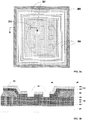
- FIG. 3A is a top view of die including the trenches
- FIG. 3B is a cross-sectional view along the line A-A' in FIG. 3A according to an embodiment of the present invention.
- a plurality of pads may include a first pad 213, which is adjacent to a first edge of the substrate.
- Trenches 301 are formed in the second passivation layer 204 between the first pad 213 and the edge of the substrate.
- the trenches are formed outside the outmost pads of the die, i.e., between the outmost dies and the edge of the die.
- the groove or trenches 301 may be annular grooves or trenches around the circuit, shown in FIG. 3A . In some embodiments, there may be a single annular trench. In other embodiments, there may be at least two annular grooves or trenches 301, so that the interfacial area can be further increased between a subsequently formed organic polymer and the die surface. Further, in the case where the die includes a sealing structure 205, grooves 301 are formed between the pads 203 and the sealing structure 205.
- grooves or trenches 301 are formed on the first passivation layer 202 outside of all pads 213. In other words, the etching of the second passivation layer is stopped on the first passivation layer. It is noted that the terms groove and trench are used interchangeably in this description.
- dotted line 302 separates the second passivation layer into two regions. The first region, to the right of dotted line 302, the second passivation layer is disposed over the pads and is higher than the second region to the left of dotted line 302 which does not overlie the pads.
- the trenches 301 are disposed at a certain distance away from dotted line 302.
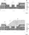
- FIG. 4 is a cross-sectional view illustrating a trench formation according to another embodiment of the present invention.
- groove or grooves 301 may be extended into the first passivation layer 202.
- the first passivation layer 202 may be a laminated layer including a first dielectric layer (e.g., an oxide layer 222), a second dielectric layer (e.g., nitride layer 212) and a third dielectric layer (e.g., the oxide layer 222).
- Different dielectric layers in the first passivation layer can be used as an etch stop layer during the etching of the second passivation layer.
- the depth of etching can be selected such that grooves or trenches 301 can extend into the first passivation layer 202 at various depths, to further increase the interfacial area of the subsequently formed organic polymer in the die surface.
- organic polymer 501 is formed to cover the die and extend into the trenches to thereby form the package.
- Organic polymer 501 maybe, for example, a polyimide or an epoxy resin.
- organic polymer 501 fills trenches 301. Thereafter, organic polymer 501 may undergo a curing treatment (e.g., thermal dehydration treatment).
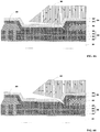
- FIGS. 6A and 6B are cross-sectional view diagrams illustrating a curing process of the organic polymer according to a conventional process.
- the organic polymer 501 is shown to contract during a curing treatment.
- the shrinkage of organic polymer 501 causes stress on the second passivation layer 204, leading to deformation and/or a peeling edge.
- pads 203 under the second passivation layer 203 may expand due to thermal expansion, so as to press the second passivation layer 204. This can lead to cracking in second passivation layer 204 in the vicinity of the stepped region near the pas 203.
- FIG. 6B is a cross-section view diagram illustrating a conventional die package undergoing an unbiased highly accelerated stress test (uHAST). Under the high temperature and high humidity test condition, the cracks can further increase, which can ultimately cause pads 203 to be exposed, and become susceptible to corrosion, resulting in chip failures.
- uHAST highly accelerated stress test
- FIG. 7 is a cross-section view diagram illustrating a curing process of a die package according to an embodiment of the present invention.
- part of organic polymer 501 is extended into trenches 301.
- the contact area between the organic polymer and the die is increased, leading to enhanced adhesion and better stress distribution.
- the stress on the second passivation layer caused by the shrinkage or contraction of the organic polymer can be reduced or avoided. It is less likely that pads 203 are exposed to cause corrosion and failure. The reliability and yield of the package can be improved.
- the present invention also provides a package as illustrated in FIG. 5 .
- the package includes a die, which includes a substrate 201 having a circuit, a first passivation layer 202 on the substrate, a plurality of pads 203 on the first passivation layer, and a second passivation layer 204 disposed on the first passivation layer and covering the plurality of pads.
- the package also includes one or more trenches 301 in a portion of the second passivation layer that overlies a portion of the first passivation layer on the outside of the plurality of pads.
- the package also includes an organic polymer overlying the die and filling the trenches.
- the first passivation layer 202 may include a stack of one or more nitride layers 212 and one or more oxide layers 222
- the second passivation layer 204 may include one or more nitride layers 224 and one or more oxide layers 214.
- trenches 301 can extend into the first passivation layer 202.
- the first passivation layer 202 may include a first dielectric layer, a second dielectric layer stack, and a third dielectric layer.
- trenches 301 can stop at the first, second, or third dielectric layer.
- the second passivation layer stops at the second dielectric layer.
- the plurality of pads may include a pad 203 adjacent to a first edge of the substrate or die.
- pad 203 is the outermost pad of the plurality of pads.
- Trench 301 is formed in the second passivation layer closest to the outer edge of the substrate.
- the edge region of the pad array is susceptible to stress buildup, because of the rising step of the second passivation layer over the pads.
- one or more trenches 301 may be annular grooves. In some embodiments, there are two or more annular trenches or grooves.
- the package may also include sealing structures, e. g., a seal ring 205 in the vicinity of the die edge around the circuit, and trenches 301 can be located between the pads 203 and the seal structure 205.
Landscapes
- Engineering & Computer Science (AREA)
- Structures Or Materials For Encapsulating Or Coating Semiconductor Devices Or Solid State Devices (AREA)
- Manufacturing & Machinery (AREA)
- Chemical & Material Sciences (AREA)
- Ceramic Engineering (AREA)
- Internal Circuitry In Semiconductor Integrated Circuit Devices (AREA)
Abstract
Description
- This application claims priority to
Chinese patent application No. 201610263531.9, filed on April 26, 2016 - The present invention relates to the field of semiconductor technology. Embodiments of the invention relate to integrated circuit package structures and manufacturing methods.
- Wafer level ball grid array package (WLBGA) is an advanced packaging technology. Due to its ability to save volume and allow maximum engagement requirement, WLBGA has been widely used. However, the inventors have found that, in devices having small geometries, existing WLBGA technologies suffer from a number of drawbacks. These drawbacks can include cracking in a passivation layer overlying the pads due to stress caused by an organic polymer covering the device. As a result, the bonding pads can be exposed or eroded, leading to chip failures. This is a typical problem in the conventional chip package integration process.
- Further, in more advanced packaging technologies, the device size is further reduced and the thermal budget is higher. Therefore, the film stress becomes relatively larger, and the problems described above can become more severe.
- Therefore, there is an urgent need for a packaging technology that is capable of alleviating the problem of the passivation layer cracking.
- It is an object of the present invention to provide a packaging technology that is capable of alleviating the problem of the passivation layer cracking.
- A first aspect of the present invention provides a method of forming a package. The method includes providing a die. The die includes a substrate having a circuit, a first passivation layer on the substrate, a plurality of pads on the first passivation layer, and a second passivation layer disposed on the first passivation layer and covering the plurality of pads. The method also includes forming one or more trenches by etching the second passivation layer that overlies a portion of the first passivation layer on the outside of the plurality of pads, and forming an organic polymer overlying the die after the one or more trenches are formed, thereby forming the package.
- By the present invention can reduce or suppress the cracking of the passivation layer overlying the bonding pads caused by stress in the package. The trenches at the edges of the bonding pads area can increase the contact area between the organic polymer and the passivation layer over the bonding pads. The adhesion of the organic polymer and stress distribution can be improved, reducing the stress between the polymer and the passivation layer. As a result, the reliability and yield of the package can be improved.
- Preferably, the plurality of pads includes a first pad, which is adjacent to an edge of the substrate. The first pad is closer to said edge of the substrate than other pads. The one or more trenches are formed in the second passivation layer overlying a portion of the first passivation layer outside the first pad.
- Preferably, the one or more trenches are located at a preset distance from a protruding portion of the second passivation layer overlying the first pad.
- Preferably, the method also includes curing the organic polymer.
- Preferably, the one or more trenches extend into the first passivation layer.
- Preferably, the first passivation layer includes a first dielectric layer, a second dielectric layer, and the third dielectric layer, and the method also includes etching the first passivation layer using the second dielectric layer as an etch stop layer.
- Preferably, each of the one or more trenches is an annular trench surrounding the circuit.
- Preferably, the package includes at least two annular trenches.
- Preferably, the die further includes a sealing structure around the circuit in the vicinity of the die edge, and the one or more trenches are located between the pad and the sealing structure.
- Preferably, the first passivation layer includes a nitride layer and an oxide layer, and the second passivation layer includes a nitride layer and an oxide layer.
- A second aspect of the present invention provides a package, e. g. an integrated circuit package. The integrated circuit package includes a die. The die has a substrate having a circuit, a first passivation layer on the substrate, a plurality of pads on the first passivation layer, and a second passivation layer disposed on the first passivation layer and covering the plurality of pads. The package also includes one or more trenches in the second passivation layer that overlies a portion of the first passivation layer on the outside of the plurality of pads, and an organic polymer overlying the die and filling the one or more trenches is formed, thereby forming the package.
- Preferably, the plurality of pads includes a first pad adjacent to an edge of the substrate. The first pad is closer to the edge of the substrate than other pads. The one or more trenches are formed in the second passivation layer overlying a portion of the first passivation layer outside the first pad.
- Preferably, the one or more trenches are located at a preset distance from a protruding portion of the second passivation layer overlying the first pad.
- Preferably, the first passivation layer includes a first dielectric layer, a second dielectric layer, and the third dielectric layer, and the one or more trenches extend through the first dielectric layer and stop at the second insulating dielectric layer.
- Preferably, the one or more trenches extend into the first passivation layer.
- Preferably, each of the one or more trenches is an annular trench surrounding the circuit.
- Preferably, the package includes at least two annular trenches.
- Preferably, the die further includes a sealing structure around the circuit in the vicinity of the die edge, and the one or more trenches are located between the pad and the sealing structure.
- Preferably, the first passivation layer comprises a nitride layer and an oxide layer, and the second passivation layer comprises a nitride layer and an oxide layer.
- The following description, together with the accompanying drawings, will provide further understanding of the nature and advantages of the claimed invention.
-
-
FIG. 1 is a simplified flowchart illustrating a method for manufacturing a package according to an embodiment of the present invention. -
FIG. 2 is a simplified cross-sectional diagram illustrating a view of a die according to an embodiment of the present invention. -
FIG. 3A is a top view of a die including the trenches, andFIG. 3B is a cross-sectional view along the line A-A' inFIG. 3A according to an embodiment of the present invention. -
FIG. 4 is a cross-sectional view illustrating a trench formation according to another embodiment of the present invention. -
FIG. 5 is a cross-sectional view illustrating polymer filling the trenches according to an embodiment of the present invention. -
FIGS. 6A and 6B are cross-sectional view diagrams illustrating a curing process of the organic polymer according to a conventional process. -
FIG. 7 is a cross-section view diagram illustrating a curing process of a die package according to an embodiment of the present invention. - The drawings of various exemplary embodiments of the present invention will be described in detail. It should be noted that, unless otherwise specified, the relative arrangement set forth in these embodiments, components and steps, the numerical expressions, and values do not limit the present invention. At the same time, it should be appreciated that, for ease of description, the dimensions of the various parts are not illustrated in the drawings according to the actual proportional relationship.
- The following description of exemplary embodiments is merely illustrative of the present invention and in no way intends to impose any restrictions on its use or application. Techniques, methods, and equipment known to someone of ordinary skill in the relevant art may not be discussed in detail, but in appropriate cases, the techniques, methods and equipment should be considered as part of the specification.
- In all the examples shown and discussed, any specific value is to be construed as merely illustrative, and not as a limitation. Accordingly, another exemplary embodiment may have different values. It should be also noted that like reference numerals and letters refer to similar items in the following figures, and thus once an item is defined in one figure, it need not be further discussed in subsequent figures.
- In the package of semiconductor dies, the ball grid array is covered with a passivation layer, which in turn is covered by organic polymers (for example, epoxy or polyimide). The inventors have discovered that, during thermal treatment, the organic polymer layer is contracted, dragging up the passivation layer. On the other hand, the bonding pads under the passivation layer are expanded due to heat treatment, pressing against the passivation layer. Further, the inventors have identified that the stress on the passivation layer tends to concentrate near the step region or protruding region of the passivation layer at the edge of the pads. The thermal mismatch between the pads and the passivation layer can, in the passivation layer near the step region, cause fatigue, leading to cracking. Moreover, subsequent stability tests, for example, the unbiased highly accelerated stress test (uHAST), can further increase the cracking of the passivation layer. The cracks in the passivation layer can ultimately cause the bonding pads to be exposed. Embodiments of the present invention provide methods and devices that address the problems described above.
-
FIG. 1 is a simplified flowchart illustrating a method for manufacturing a package according to an embodiment of the present invention. The steps in this flowchart are further described below with reference toFIGS. 2-7 . - As shown in
FIG. 1 , instep 101, the method includes providing a die.FIG. 2 is a simplified cross-sectional diagram illustrating a view of a die according to an embodiment of the present invention. As shown inFIG. 2 , adie 200 includes asubstrate 201, which may be a silicon substrate having a circuit or other semiconductor material substrates. Here, for clarity, the circuit is not shown inFIG. 2 .Die 200 further includes afirst passivation layer 202 on thesubstrate 201. In one embodiment, thefirst passivation layer 202 may include a stack ofnitride layer 212 andoxide layer 222. For example, thefirst passivation layer 202 may include a plurality of nitride layer 212 (e.g., SiN) and oxide layer 222 (e.g., formed from TEOS, tetraethoxysilane). In another embodiment, thefirst passivation layer 202 may be formed by anoxide layer 222, anitride layer 212, and anoxide layer 222 forming a three-layer stack. As a non-limiting example, the thickness of thenitride layer 212 may be about 750 Angstroms (A), and the thickness of theoxide layer 222 may be about 4000 Å. - Die 200 can also include a plurality of
bonding pads 203 on thefirst passivation layer 202. It is noted thatFIG. 2 merely schematically shows apad 203 as an example. Those skilled in the art will readily understand that a plurality ofpads 203 may be distributed on thefirst passivation layer 202. In an embodiment,pad 203 may be an aluminum (Al) pad, and the thickness ofpad 203 can be, for example, about 14.5 nm. - Die 200 can further include a
second passivation layer 204 overlying thefirst passivation layer 202 and covering the plurality ofpads 203. Thesecond passivation layer 204 may include a stack of anoxide layer 214 andnitride layer 224.Oxide layer 214 may be an oxide formed from TEOS, and anitride layer 224 is typically silicon nitride, SiN, for example. As a non-limiting example, the thickness of theoxide layer 214 may be about 4000 angstroms, and the thickness of thenitride layer 224 may be about 6000 angstroms. In an embodiment, thedie 200 may also include a sealingstructure 205 surrounding the circuit in the vicinity of the die edge, e.g., a seal ring. - Returning to
FIG. 1 , instep 103, the second passivation layer is etched to form trenches, which are located on the first passivation layer outside the plurality of die pads.FIG. 3A is a top view of die including the trenches, andFIG. 3B is a cross-sectional view along the line A-A' inFIG. 3A according to an embodiment of the present invention. As shown inFIG. 3A , a plurality of pads may include afirst pad 213, which is adjacent to a first edge of the substrate.Trenches 301 are formed in thesecond passivation layer 204 between thefirst pad 213 and the edge of the substrate. As shown, the trenches are formed outside the outmost pads of the die, i.e., between the outmost dies and the edge of the die. - In an embodiment, the groove or
trenches 301 may be annular grooves or trenches around the circuit, shown inFIG. 3A . In some embodiments, there may be a single annular trench. In other embodiments, there may be at least two annular grooves ortrenches 301, so that the interfacial area can be further increased between a subsequently formed organic polymer and the die surface. Further, in the case where the die includes a sealingstructure 205,grooves 301 are formed between thepads 203 and the sealingstructure 205. - As shown in
FIG. 3B , grooves ortrenches 301 are formed on thefirst passivation layer 202 outside of allpads 213. In other words, the etching of the second passivation layer is stopped on the first passivation layer. It is noted that the terms groove and trench are used interchangeably in this description. InFIG. 3B , dottedline 302 separates the second passivation layer into two regions. The first region, to the right ofdotted line 302, the second passivation layer is disposed over the pads and is higher than the second region to the left ofdotted line 302 which does not overlie the pads. In an embodiment, thetrenches 301 are disposed at a certain distance away from dottedline 302. -
FIG. 4 is a cross-sectional view illustrating a trench formation according to another embodiment of the present invention. As shown inFIG. 4 , groove orgrooves 301 may be extended into thefirst passivation layer 202. In one implementation, thefirst passivation layer 202 may be a laminated layer including a first dielectric layer (e.g., an oxide layer 222), a second dielectric layer (e.g., nitride layer 212) and a third dielectric layer (e.g., the oxide layer 222). Different dielectric layers in the first passivation layer can be used as an etch stop layer during the etching of the second passivation layer. The depth of etching can be selected such that grooves ortrenches 301 can extend into thefirst passivation layer 202 at various depths, to further increase the interfacial area of the subsequently formed organic polymer in the die surface. - Referring to
FIG. 1 again, instep 105,. As shown inFIG. 5 anorganic polymer 501 is formed to cover the die and extend into the trenches to thereby form the package.Organic polymer 501 maybe, for example, a polyimide or an epoxy resin. In some embodiments,organic polymer 501 fillstrenches 301. Thereafter,organic polymer 501 may undergo a curing treatment (e.g., thermal dehydration treatment). -
FIGS. 6A and 6B are cross-sectional view diagrams illustrating a curing process of the organic polymer according to a conventional process. InFIG. 6A , theorganic polymer 501 is shown to contract during a curing treatment. The shrinkage oforganic polymer 501 causes stress on thesecond passivation layer 204, leading to deformation and/or a peeling edge.. Further,pads 203 under thesecond passivation layer 203 may expand due to thermal expansion, so as to press thesecond passivation layer 204. This can lead to cracking insecond passivation layer 204 in the vicinity of the stepped region near thepas 203.FIG. 6B is a cross-section view diagram illustrating a conventional die package undergoing an unbiased highly accelerated stress test (uHAST). Under the high temperature and high humidity test condition, the cracks can further increase, which can ultimately causepads 203 to be exposed, and become susceptible to corrosion, resulting in chip failures. -
FIG. 7 is a cross-section view diagram illustrating a curing process of a die package according to an embodiment of the present invention. As shown inFIG. 7 , part oforganic polymer 501 is extended intotrenches 301. As a result, the contact area between the organic polymer and the die is increased, leading to enhanced adhesion and better stress distribution. Under this condition, the stress on the second passivation layer caused by the shrinkage or contraction of the organic polymer can be reduced or avoided. It is less likely thatpads 203 are exposed to cause corrosion and failure. The reliability and yield of the package can be improved. - According to some embodiments, the present invention also provides a package as illustrated in
FIG. 5 . As shown inFIG. 5 , the package includes a die, which includes asubstrate 201 having a circuit, afirst passivation layer 202 on the substrate, a plurality ofpads 203 on the first passivation layer, and asecond passivation layer 204 disposed on the first passivation layer and covering the plurality of pads. The package also includes one ormore trenches 301 in a portion of the second passivation layer that overlies a portion of the first passivation layer on the outside of the plurality of pads. The package also includes an organic polymer overlying the die and filling the trenches. A portion of the second passivation layer overlying the pads protrudes above the other portion of the second passivation layer not covering pads. In some embodiments, thefirst passivation layer 202 may include a stack of one ormore nitride layers 212 and one ormore oxide layers 222, and thesecond passivation layer 204 may include one ormore nitride layers 224 and one or more oxide layers 214. - In some embodiments,
trenches 301 can extend into thefirst passivation layer 202. In some embodiments, thefirst passivation layer 202 may include a first dielectric layer, a second dielectric layer stack, and a third dielectric layer. In this case,trenches 301 can stop at the first, second, or third dielectric layer. In a particular embodiment, the second passivation layer stops at the second dielectric layer. - In one embodiment, as shown in
FIG. 3A , the plurality of pads may include apad 203 adjacent to a first edge of the substrate or die. In other words, pad 203 is the outermost pad of the plurality of pads.Trench 301 is formed in the second passivation layer closest to the outer edge of the substrate. As described above, the edge region of the pad array is susceptible to stress buildup, because of the rising step of the second passivation layer over the pads. In addition, one ormore trenches 301 may be annular grooves. In some embodiments, there are two or more annular trenches or grooves. In one embodiment, the package may also include sealing structures, e. g., aseal ring 205 in the vicinity of the die edge around the circuit, andtrenches 301 can be located between thepads 203 and theseal structure 205. - Thus, a device package structure and a manufacturing method have been described in detail. Some of the features of the preferred embodiments of the present invention could be used to advantage without the corresponding use of other features.
Claims (15)
- A method of forming a package, comprising:providing a die, the die comprising:a substrate having a circuit;a first passivation layer on the substrate;a plurality of pads on the first passivation layer; anda second passivation layer disposed on the first passivation layer and covering the plurality of pads;forming one or more trenches by etching the second passivation layer that overlies a portion of the first passivation layer on the outside of the plurality of pads; andforming an organic polymer overlying the die after the one or more trenches are formed, thereby forming the package.
- The method according to claim 1,
wherein the plurality of pads comprises a first pad, the first pad being adjacent to an edge of the substrate, the first pad being closer to said edge of the substrate than other pads;
wherein the one or more trenches are formed in the second passivation layer overlying a portion of the first passivation layer outside the first pad. - The method according to claim 2,
wherein the one or more trenches are located at a preset distance from a protruding portion of the second passivation layer overlying the first pad. - The method according to any one of the claims 1-3, further comprising:curing the organic polymer.
- The method of any one of the claims 1-4,
wherein the one or more trenches extend into the first passivation layer; and/or
wherein the first passivation layer comprises a first dielectric layer, a second dielectric layer, and the third dielectric layer, and wherein the method further comprises etching the first passivation layer using the second dielectric layer as an etch stop layer. - The method according to any one of the claims 1-5,
wherein each of the one or more trenches is an annular trench surrounding the circuit; and
wherein preferably: the one or two trenches comprise at least two annular trenches. - The method according to any one of the claims 1-6,
wherein said die further comprises a sealing structure around the circuit in the vicinity of the die edge, and the one or more trenches are located between the pad and the sealing structure; and/or
wherein the first passivation layer comprises a nitride layer and an oxide layer, and the second passivation layer comprises a nitride layer and an oxide layer. - A package, comprising:a die, wherein the die comprises: a substrate having a circuit; a first passivation layer on the substrate; a plurality of pads on the first passivation layer; and a second passivation layer disposed on the first passivation layer and covering the plurality of pads;one or more trenches in the second passivation layer that overlies a portion of the first passivation layer on the outside of the plurality of pads; andan organic polymer overlying the die and filling the one or more trenches, thereby forming the package.
- The package according to claim 8,
wherein the plurality of pads comprises a first pad, the first pad being adjacent to an edge of the substrate, the first pad being closer to said edge of the substrate than other pads;
wherein the one or more trenches are formed in the second passivation layer overlying a portion of the first passivation layer outside the first pad. - The package according to claim 9, wherein the one or more trenches are located at a preset distance from a protruding portion of the second passivation layer overlying the first pad.
- The package of any one of the claims 8-10, wherein the first passivation layer comprises a first dielectric layer, a second dielectric layer, and the third dielectric layer, and the one or more trenches extend through the first dielectric layer and stop at the second insulating dielectric layer.
- The package of any one of the claims 8-11,
wherein the one or more trenches extend into the first passivation layer. - The package of any one of the claims 8-12,
wherein each of the one or more trenches is an annular trench surrounding the circuit; and
wherein preferably: the one or two trenches comprise at least two annular trenches. - The package of any one of the claims 8-13,
wherein the die further comprises a sealing structure around the circuit in the vicinity of the die edge, and the one or more trenches are located between the pad and the sealing structure. - The package of any one of the claims 8-14,
wherein the first passivation layer comprises a nitride layer and an oxide layer, and the second passivation layer comprises a nitride layer and an oxide layer.
Applications Claiming Priority (1)
| Application Number | Priority Date | Filing Date | Title |
|---|---|---|---|
| CN201610263531.9A CN107316817B (en) | 2016-04-26 | 2016-04-26 | Package and method of making the same |
Publications (1)
| Publication Number | Publication Date |
|---|---|
| EP3240023A1 true EP3240023A1 (en) | 2017-11-01 |
Family
ID=58671371
Family Applications (1)
| Application Number | Title | Priority Date | Filing Date |
|---|---|---|---|
| EP17167238.9A Withdrawn EP3240023A1 (en) | 2016-04-26 | 2017-04-20 | Method and apparatus for semiconductor packaging |
Country Status (3)
| Country | Link |
|---|---|
| US (1) | US10636719B2 (en) |
| EP (1) | EP3240023A1 (en) |
| CN (1) | CN107316817B (en) |
Families Citing this family (8)
| Publication number | Priority date | Publication date | Assignee | Title |
|---|---|---|---|---|
| CN109920772B (en) * | 2017-12-12 | 2021-07-13 | 中芯国际集成电路制造(上海)有限公司 | Package structure and method for forming the same |
| CN110838471B (en) * | 2018-08-16 | 2025-01-14 | 飞锃半导体(上海)有限公司 | Chip edge structure and manufacturing method |
| JP7149907B2 (en) * | 2019-09-04 | 2022-10-07 | 三菱電機株式会社 | Semiconductor devices and semiconductor elements |
| CN113130413B (en) * | 2019-12-30 | 2024-09-06 | 联华电子股份有限公司 | Semiconductor element packaging structure and manufacturing method thereof |
| KR102949944B1 (en) | 2021-04-28 | 2026-04-07 | 삼성전자주식회사 | Semiconductor packages |
| CN219180514U (en) * | 2021-11-26 | 2023-06-13 | 意法半导体股份有限公司 | Semiconductor Devices and Electronic Devices |
| CN116504748A (en) * | 2022-01-25 | 2023-07-28 | 意法半导体有限公司 | Thick bond pad structure for wire bond stress reduction |
| CN117116888B (en) * | 2023-01-16 | 2025-01-17 | 荣耀终端有限公司 | Semiconductor packaging structure and preparation method thereof, and electronic device |
Citations (8)
| Publication number | Priority date | Publication date | Assignee | Title |
|---|---|---|---|---|
| US6492247B1 (en) * | 2000-11-21 | 2002-12-10 | International Business Machines Corporation | Method for eliminating crack damage induced by delaminating gate conductor interfaces in integrated circuits |
| US20050167824A1 (en) * | 2004-01-30 | 2005-08-04 | Chartered Semiconductor Manufacturing Ltd. | Integrated circuit with protective moat |
| US20080277765A1 (en) * | 2007-05-10 | 2008-11-13 | International Business Machines Corporation | Inhibiting damage from dicing and chip packaging interaction failures in back end of line structures |
| US20090032909A1 (en) * | 2007-08-03 | 2009-02-05 | Brofman Peter J | Semiconductor chips with crack stop regions for reducing crack propagation from chip edges/corners |
| US20090115024A1 (en) * | 2007-11-01 | 2009-05-07 | Jeng Shin-Puu | Seal ring structure with improved cracking protection and reduced problems |
| US20100006984A1 (en) * | 2007-03-30 | 2010-01-14 | Fujitsu Microelectronics Limited | Semiconductor device |
| US20110006389A1 (en) * | 2009-07-08 | 2011-01-13 | Lsi Corporation | Suppressing fractures in diced integrated circuits |
| US20140116760A1 (en) * | 2012-10-25 | 2014-05-01 | United Microelectronics Corp. | Bond pad structure and method of manufacturing the same |
Family Cites Families (11)
| Publication number | Priority date | Publication date | Assignee | Title |
|---|---|---|---|---|
| TW396454B (en) * | 1997-06-24 | 2000-07-01 | Matsushita Electrics Corporati | Semiconductor device and method for fabricating the same |
| US6297554B1 (en) * | 2000-03-10 | 2001-10-02 | United Microelectronics Corp. | Dual damascene interconnect structure with reduced parasitic capacitance |
| US20050026397A1 (en) * | 2003-07-28 | 2005-02-03 | International Business Machines Corporation | Crack stop for low k dielectrics |
| TWI229438B (en) * | 2004-01-30 | 2005-03-11 | Advanced Semiconductor Eng | Substrate for packaging IC device and method for manufacturing the same |
| US20080182398A1 (en) * | 2007-01-30 | 2008-07-31 | Carpenter Burton J | Varied Solder Mask Opening Diameters Within a Ball Grid Array Substrate |
| US9466666B2 (en) * | 2012-05-03 | 2016-10-11 | Analog Devices Global | Localized strain relief for an integrated circuit |
| US20130337615A1 (en) * | 2012-05-25 | 2013-12-19 | Applied Materials, Inc. | Polymer hot-wire chemical vapor deposition in chip scale packaging |
| US9425121B2 (en) * | 2013-09-11 | 2016-08-23 | Taiwan Semiconductor Manufacturing Company, Ltd. | Integrated fan-out structure with guiding trenches in buffer layer |
| CN104091793B (en) * | 2014-07-18 | 2016-09-21 | 华进半导体封装先导技术研发中心有限公司 | Improve micro bump and the manufacture method of reliability |
| JP6033522B1 (en) * | 2014-12-18 | 2016-11-30 | 三菱電機株式会社 | Insulated circuit board, power module and power unit |
| JP2016131179A (en) * | 2015-01-13 | 2016-07-21 | ソニー株式会社 | SEMICONDUCTOR DEVICE, SEMICONDUCTOR DEVICE MANUFACTURING METHOD, SOLID-STATE IMAGING ELEMENT, IMAGING DEVICE, AND ELECTRONIC DEVICE |
-
2016
- 2016-04-26 CN CN201610263531.9A patent/CN107316817B/en active Active
-
2017
- 2017-04-10 US US15/483,836 patent/US10636719B2/en active Active
- 2017-04-20 EP EP17167238.9A patent/EP3240023A1/en not_active Withdrawn
Patent Citations (8)
| Publication number | Priority date | Publication date | Assignee | Title |
|---|---|---|---|---|
| US6492247B1 (en) * | 2000-11-21 | 2002-12-10 | International Business Machines Corporation | Method for eliminating crack damage induced by delaminating gate conductor interfaces in integrated circuits |
| US20050167824A1 (en) * | 2004-01-30 | 2005-08-04 | Chartered Semiconductor Manufacturing Ltd. | Integrated circuit with protective moat |
| US20100006984A1 (en) * | 2007-03-30 | 2010-01-14 | Fujitsu Microelectronics Limited | Semiconductor device |
| US20080277765A1 (en) * | 2007-05-10 | 2008-11-13 | International Business Machines Corporation | Inhibiting damage from dicing and chip packaging interaction failures in back end of line structures |
| US20090032909A1 (en) * | 2007-08-03 | 2009-02-05 | Brofman Peter J | Semiconductor chips with crack stop regions for reducing crack propagation from chip edges/corners |
| US20090115024A1 (en) * | 2007-11-01 | 2009-05-07 | Jeng Shin-Puu | Seal ring structure with improved cracking protection and reduced problems |
| US20110006389A1 (en) * | 2009-07-08 | 2011-01-13 | Lsi Corporation | Suppressing fractures in diced integrated circuits |
| US20140116760A1 (en) * | 2012-10-25 | 2014-05-01 | United Microelectronics Corp. | Bond pad structure and method of manufacturing the same |
Also Published As
| Publication number | Publication date |
|---|---|
| US10636719B2 (en) | 2020-04-28 |
| US20170309536A1 (en) | 2017-10-26 |
| CN107316817A (en) | 2017-11-03 |
| CN107316817B (en) | 2020-08-25 |
Similar Documents
| Publication | Publication Date | Title |
|---|---|---|
| US10636719B2 (en) | Semiconductor packaging with reduced cracking defects | |
| US11081462B2 (en) | Method for manufacturing a bonding structure | |
| US9287221B2 (en) | Method for forming crack stop structure | |
| EP3154085A1 (en) | Semiconductor package structure and method for forming the same | |
| KR20160052330A (en) | Semiconductor device and method for manufacturing semiconductor device | |
| JP4360881B2 (en) | Semiconductor device including multilayer wiring and manufacturing method thereof | |
| US20140015136A1 (en) | Ic device including package structure and method of forming the same | |
| US10068825B2 (en) | Semiconductor device | |
| US8803297B2 (en) | Semiconductor device including a stress relief layer and method of manufacturing | |
| JP2014033053A (en) | Semiconductor device and method for manufacturing the same | |
| US10930541B2 (en) | Method of forming a chip arrangement, chip arrangement, method of forming a chip package, and chip package | |
| US20040124546A1 (en) | Reliable integrated circuit and package | |
| US11069627B2 (en) | Scribe seals and methods of making | |
| CN105977226A (en) | Seal ring and method for preventing chip from being damaged during cutting | |
| TW201810557A (en) | Chip size single-sided stress release wafer size package structure and manufacturing method thereof | |
| CN109920772B (en) | Package structure and method for forming the same | |
| US7488993B2 (en) | Semiconductor device and method of manufacturing the same | |
| US10892239B1 (en) | Bond pad reliability of semiconductor devices | |
| US12094758B2 (en) | Semiconductor structure and method for manufacturing the same | |
| US9806034B1 (en) | Semiconductor device with protected sidewalls and methods of manufacturing thereof | |
| JP4361517B2 (en) | Semiconductor device and manufacturing method thereof | |
| US10665547B2 (en) | Semiconductor device and method of manufacturing thereof | |
| KR20090128133A (en) | Manufacturing Method of Semiconductor Device | |
| CN108666277A (en) | Encapsulating structure and forming method thereof | |
| CN105575914B (en) | Semiconductor device |
Legal Events
| Date | Code | Title | Description |
|---|---|---|---|
| PUAI | Public reference made under article 153(3) epc to a published international application that has entered the european phase |
Free format text: ORIGINAL CODE: 0009012 |
|
| STAA | Information on the status of an ep patent application or granted ep patent |
Free format text: STATUS: THE APPLICATION HAS BEEN PUBLISHED |
|
| AK | Designated contracting states |
Kind code of ref document: A1 Designated state(s): AL AT BE BG CH CY CZ DE DK EE ES FI FR GB GR HR HU IE IS IT LI LT LU LV MC MK MT NL NO PL PT RO RS SE SI SK SM TR |
|
| AX | Request for extension of the european patent |
Extension state: BA ME |
|
| STAA | Information on the status of an ep patent application or granted ep patent |
Free format text: STATUS: REQUEST FOR EXAMINATION WAS MADE |
|
| 17P | Request for examination filed |
Effective date: 20180427 |
|
| RBV | Designated contracting states (corrected) |
Designated state(s): AL AT BE BG CH CY CZ DE DK EE ES FI FR GB GR HR HU IE IS IT LI LT LU LV MC MK MT NL NO PL PT RO RS SE SI SK SM TR |
|
| RAP1 | Party data changed (applicant data changed or rights of an application transferred) |
Owner name: SEMICONDUCTOR MANUFACTURING INTERNATIONAL (SHANGHA Owner name: SEMICONDUCTOR MANUFACTURING INTERNATIONAL (BEIJING |
|
| STAA | Information on the status of an ep patent application or granted ep patent |
Free format text: STATUS: EXAMINATION IS IN PROGRESS |
|
| 17Q | First examination report despatched |
Effective date: 20190829 |
|
| STAA | Information on the status of an ep patent application or granted ep patent |
Free format text: STATUS: THE APPLICATION IS DEEMED TO BE WITHDRAWN |
|
| 18D | Application deemed to be withdrawn |
Effective date: 20200109 |