EP3237943B1 - Oxidation and moisture barrier layers for wire grid polarizer - Google Patents
Oxidation and moisture barrier layers for wire grid polarizer Download PDFInfo
- Publication number
- EP3237943B1 EP3237943B1 EP16773995.2A EP16773995A EP3237943B1 EP 3237943 B1 EP3237943 B1 EP 3237943B1 EP 16773995 A EP16773995 A EP 16773995A EP 3237943 B1 EP3237943 B1 EP 3237943B1
- Authority
- EP
- European Patent Office
- Prior art keywords
- ribs
- barrier
- conformal
- coating
- layer
- Prior art date
- Legal status (The legal status is an assumption and is not a legal conclusion. Google has not performed a legal analysis and makes no representation as to the accuracy of the status listed.)
- Active
Links
- 230000004888 barrier function Effects 0.000 title claims description 16
- 238000007254 oxidation reaction Methods 0.000 title description 11
- 230000003647 oxidation Effects 0.000 title description 10
- 238000000576 coating method Methods 0.000 claims description 145
- 239000011248 coating agent Substances 0.000 claims description 140
- 239000000463 material Substances 0.000 claims description 53
- 229910052710 silicon Inorganic materials 0.000 claims description 27
- XLYOFNOQVPJJNP-UHFFFAOYSA-N water Substances O XLYOFNOQVPJJNP-UHFFFAOYSA-N 0.000 claims description 27
- XUIMIQQOPSSXEZ-UHFFFAOYSA-N Silicon Chemical compound [Si] XUIMIQQOPSSXEZ-UHFFFAOYSA-N 0.000 claims description 26
- 239000010703 silicon Substances 0.000 claims description 26
- 239000000126 substance Substances 0.000 claims description 20
- VYPSYNLAJGMNEJ-UHFFFAOYSA-N Silicium dioxide Chemical compound O=[Si]=O VYPSYNLAJGMNEJ-UHFFFAOYSA-N 0.000 claims description 19
- BLRPTPMANUNPDV-UHFFFAOYSA-N Silane Chemical compound [SiH4] BLRPTPMANUNPDV-UHFFFAOYSA-N 0.000 claims description 18
- 229910000077 silane Inorganic materials 0.000 claims description 18
- 239000000758 substrate Substances 0.000 claims description 16
- 238000007740 vapor deposition Methods 0.000 claims description 16
- 229910052732 germanium Inorganic materials 0.000 claims description 15
- GNPVGFCGXDBREM-UHFFFAOYSA-N germanium atom Chemical compound [Ge] GNPVGFCGXDBREM-UHFFFAOYSA-N 0.000 claims description 15
- 125000003118 aryl group Chemical group 0.000 claims description 14
- UEZVMMHDMIWARA-UHFFFAOYSA-M phosphonate Chemical compound [O-]P(=O)=O UEZVMMHDMIWARA-UHFFFAOYSA-M 0.000 claims description 14
- 125000000217 alkyl group Chemical group 0.000 claims description 13
- TWNQGVIAIRXVLR-UHFFFAOYSA-N oxo(oxoalumanyloxy)alumane Chemical compound O=[Al]O[Al]=O TWNQGVIAIRXVLR-UHFFFAOYSA-N 0.000 claims description 13
- 125000001165 hydrophobic group Chemical group 0.000 claims description 11
- 238000000034 method Methods 0.000 claims description 11
- 229910052814 silicon oxide Inorganic materials 0.000 claims description 9
- 229910052581 Si3N4 Inorganic materials 0.000 claims description 8
- 229910000449 hafnium oxide Inorganic materials 0.000 claims description 8
- WIHZLLGSGQNAGK-UHFFFAOYSA-N hafnium(4+);oxygen(2-) Chemical compound [O-2].[O-2].[Hf+4] WIHZLLGSGQNAGK-UHFFFAOYSA-N 0.000 claims description 8
- 238000004519 manufacturing process Methods 0.000 claims description 8
- RVTZCBVAJQQJTK-UHFFFAOYSA-N oxygen(2-);zirconium(4+) Chemical compound [O-2].[O-2].[Zr+4] RVTZCBVAJQQJTK-UHFFFAOYSA-N 0.000 claims description 8
- HQVNEWCFYHHQES-UHFFFAOYSA-N silicon nitride Chemical compound N12[Si]34N5[Si]62N3[Si]51N64 HQVNEWCFYHHQES-UHFFFAOYSA-N 0.000 claims description 8
- 229910001928 zirconium oxide Inorganic materials 0.000 claims description 8
- HBMJWWWQQXIZIP-UHFFFAOYSA-N silicon carbide Chemical compound [Si+]#[C-] HBMJWWWQQXIZIP-UHFFFAOYSA-N 0.000 claims description 7
- 229910010271 silicon carbide Inorganic materials 0.000 claims description 7
- 229910052729 chemical element Inorganic materials 0.000 claims description 6
- 229910001404 rare earth metal oxide Inorganic materials 0.000 claims description 6
- 239000010410 layer Substances 0.000 description 78
- 230000010287 polarization Effects 0.000 description 19
- 125000004432 carbon atom Chemical group C* 0.000 description 16
- OKTJSMMVPCPJKN-UHFFFAOYSA-N Carbon Chemical compound [C] OKTJSMMVPCPJKN-UHFFFAOYSA-N 0.000 description 15
- 230000009286 beneficial effect Effects 0.000 description 14
- 229910052799 carbon Inorganic materials 0.000 description 14
- 238000005260 corrosion Methods 0.000 description 13
- 230000007797 corrosion Effects 0.000 description 13
- 229910052782 aluminium Inorganic materials 0.000 description 10
- XAGFODPZIPBFFR-UHFFFAOYSA-N aluminium Chemical compound [Al] XAGFODPZIPBFFR-UHFFFAOYSA-N 0.000 description 10
- 238000007689 inspection Methods 0.000 description 10
- NINIDFKCEFEMDL-UHFFFAOYSA-N Sulfur Chemical compound [S] NINIDFKCEFEMDL-UHFFFAOYSA-N 0.000 description 8
- 239000011253 protective coating Substances 0.000 description 8
- 229910052717 sulfur Inorganic materials 0.000 description 8
- 239000011593 sulfur Substances 0.000 description 8
- 125000004429 atom Chemical group 0.000 description 6
- 230000015556 catabolic process Effects 0.000 description 6
- 239000007864 aqueous solution Substances 0.000 description 5
- 238000000231 atomic layer deposition Methods 0.000 description 5
- 230000008901 benefit Effects 0.000 description 5
- 238000004140 cleaning Methods 0.000 description 5
- 238000006731 degradation reaction Methods 0.000 description 5
- 239000000428 dust Substances 0.000 description 5
- 239000010408 film Substances 0.000 description 5
- BHEPBYXIRTUNPN-UHFFFAOYSA-N hydridophosphorus(.) (triplet) Chemical compound [PH] BHEPBYXIRTUNPN-UHFFFAOYSA-N 0.000 description 5
- 229910052751 metal Inorganic materials 0.000 description 5
- 239000002184 metal Substances 0.000 description 5
- 210000002381 plasma Anatomy 0.000 description 5
- 239000000377 silicon dioxide Substances 0.000 description 5
- 235000012239 silicon dioxide Nutrition 0.000 description 5
- 238000007654 immersion Methods 0.000 description 4
- 239000007788 liquid Substances 0.000 description 4
- 230000002411 adverse Effects 0.000 description 3
- 150000001721 carbon Chemical group 0.000 description 3
- 239000003086 colorant Substances 0.000 description 3
- 230000007547 defect Effects 0.000 description 3
- 230000001419 dependent effect Effects 0.000 description 3
- 239000007789 gas Substances 0.000 description 3
- 229910044991 metal oxide Inorganic materials 0.000 description 3
- 150000004706 metal oxides Chemical class 0.000 description 3
- 239000004065 semiconductor Substances 0.000 description 3
- 239000002356 single layer Substances 0.000 description 3
- 238000001429 visible spectrum Methods 0.000 description 3
- IJGRMHOSHXDMSA-UHFFFAOYSA-N Atomic nitrogen Chemical compound N#N IJGRMHOSHXDMSA-UHFFFAOYSA-N 0.000 description 2
- RTZKZFJDLAIYFH-UHFFFAOYSA-N Diethyl ether Chemical compound CCOCC RTZKZFJDLAIYFH-UHFFFAOYSA-N 0.000 description 2
- CBENFWSGALASAD-UHFFFAOYSA-N Ozone Chemical compound [O-][O+]=O CBENFWSGALASAD-UHFFFAOYSA-N 0.000 description 2
- 230000009471 action Effects 0.000 description 2
- 230000008033 biological extinction Effects 0.000 description 2
- 230000005540 biological transmission Effects 0.000 description 2
- 229920002678 cellulose Polymers 0.000 description 2
- 238000005229 chemical vapour deposition Methods 0.000 description 2
- 230000007423 decrease Effects 0.000 description 2
- 238000000151 deposition Methods 0.000 description 2
- 230000002542 deteriorative effect Effects 0.000 description 2
- ZUOUZKKEUPVFJK-UHFFFAOYSA-N diphenyl Chemical compound C1=CC=CC=C1C1=CC=CC=C1 ZUOUZKKEUPVFJK-UHFFFAOYSA-N 0.000 description 2
- USIUVYZYUHIAEV-UHFFFAOYSA-N diphenyl ether Chemical compound C=1C=CC=CC=1OC1=CC=CC=C1 USIUVYZYUHIAEV-UHFFFAOYSA-N 0.000 description 2
- DMBHHRLKUKUOEG-UHFFFAOYSA-N diphenylamine Chemical compound C=1C=CC=CC=1NC1=CC=CC=C1 DMBHHRLKUKUOEG-UHFFFAOYSA-N 0.000 description 2
- 238000002438 flame photometric detection Methods 0.000 description 2
- -1 for example Chemical group 0.000 description 2
- 239000011521 glass Substances 0.000 description 2
- 125000004404 heteroalkyl group Chemical group 0.000 description 2
- 125000001072 heteroaryl group Chemical group 0.000 description 2
- 125000005842 heteroatom Chemical group 0.000 description 2
- 150000002430 hydrocarbons Chemical group 0.000 description 2
- 150000002484 inorganic compounds Chemical class 0.000 description 2
- 229910010272 inorganic material Inorganic materials 0.000 description 2
- 239000004973 liquid crystal related substance Substances 0.000 description 2
- 238000004518 low pressure chemical vapour deposition Methods 0.000 description 2
- 230000005291 magnetic effect Effects 0.000 description 2
- 230000003287 optical effect Effects 0.000 description 2
- 239000002245 particle Substances 0.000 description 2
- 238000005240 physical vapour deposition Methods 0.000 description 2
- 229920006254 polymer film Polymers 0.000 description 2
- 239000007787 solid Substances 0.000 description 2
- 125000001424 substituent group Chemical group 0.000 description 2
- 125000000547 substituted alkyl group Chemical group 0.000 description 2
- 125000003107 substituted aryl group Chemical group 0.000 description 2
- 239000012780 transparent material Substances 0.000 description 2
- 229910052684 Cerium Inorganic materials 0.000 description 1
- 229910052692 Dysprosium Inorganic materials 0.000 description 1
- 229910052691 Erbium Inorganic materials 0.000 description 1
- VGGSQFUCUMXWEO-UHFFFAOYSA-N Ethene Chemical group C=C VGGSQFUCUMXWEO-UHFFFAOYSA-N 0.000 description 1
- 239000005977 Ethylene Chemical group 0.000 description 1
- 229910052693 Europium Inorganic materials 0.000 description 1
- PXGOKWXKJXAPGV-UHFFFAOYSA-N Fluorine Chemical compound FF PXGOKWXKJXAPGV-UHFFFAOYSA-N 0.000 description 1
- 229910052688 Gadolinium Inorganic materials 0.000 description 1
- 229910052689 Holmium Inorganic materials 0.000 description 1
- 229910052765 Lutetium Inorganic materials 0.000 description 1
- BCXBKOQDEOJNRH-UHFFFAOYSA-N NOP(O)=O Chemical class NOP(O)=O BCXBKOQDEOJNRH-UHFFFAOYSA-N 0.000 description 1
- 229910052779 Neodymium Inorganic materials 0.000 description 1
- 229910003849 O-Si Inorganic materials 0.000 description 1
- 229910003872 O—Si Inorganic materials 0.000 description 1
- 229910052777 Praseodymium Inorganic materials 0.000 description 1
- 229910052773 Promethium Inorganic materials 0.000 description 1
- 229910052772 Samarium Inorganic materials 0.000 description 1
- 229910052771 Terbium Inorganic materials 0.000 description 1
- 229910052775 Thulium Inorganic materials 0.000 description 1
- 229910052769 Ytterbium Inorganic materials 0.000 description 1
- 230000001154 acute effect Effects 0.000 description 1
- 125000005428 anthryl group Chemical group [H]C1=C([H])C([H])=C2C([H])=C3C(*)=C([H])C([H])=C([H])C3=C([H])C2=C1[H] 0.000 description 1
- QVGXLLKOCUKJST-UHFFFAOYSA-N atomic oxygen Chemical compound [O] QVGXLLKOCUKJST-UHFFFAOYSA-N 0.000 description 1
- RWCCWEUUXYIKHB-UHFFFAOYSA-N benzophenone Chemical compound C=1C=CC=CC=1C(=O)C1=CC=CC=C1 RWCCWEUUXYIKHB-UHFFFAOYSA-N 0.000 description 1
- 239000012965 benzophenone Substances 0.000 description 1
- 235000010290 biphenyl Nutrition 0.000 description 1
- 239000004305 biphenyl Substances 0.000 description 1
- ZMIGMASIKSOYAM-UHFFFAOYSA-N cerium Chemical compound [Ce][Ce][Ce][Ce][Ce][Ce][Ce][Ce][Ce][Ce][Ce][Ce][Ce][Ce][Ce][Ce][Ce][Ce][Ce][Ce][Ce][Ce][Ce][Ce][Ce][Ce][Ce][Ce][Ce][Ce][Ce][Ce][Ce][Ce][Ce][Ce][Ce][Ce] ZMIGMASIKSOYAM-UHFFFAOYSA-N 0.000 description 1
- 230000008859 change Effects 0.000 description 1
- 239000011247 coating layer Substances 0.000 description 1
- 239000002131 composite material Substances 0.000 description 1
- 239000002178 crystalline material Substances 0.000 description 1
- 125000004122 cyclic group Chemical group 0.000 description 1
- 125000000753 cycloalkyl group Chemical group 0.000 description 1
- 125000000113 cyclohexyl group Chemical group [H]C1([H])C([H])([H])C([H])([H])C([H])(*)C([H])([H])C1([H])[H] 0.000 description 1
- 125000001511 cyclopentyl group Chemical group [H]C1([H])C([H])([H])C([H])([H])C([H])(*)C1([H])[H] 0.000 description 1
- 230000003247 decreasing effect Effects 0.000 description 1
- 125000002704 decyl group Chemical group [H]C([H])([H])C([H])([H])C([H])([H])C([H])([H])C([H])([H])C([H])([H])C([H])([H])C([H])([H])C([H])([H])C([H])([H])* 0.000 description 1
- 230000008021 deposition Effects 0.000 description 1
- 230000001627 detrimental effect Effects 0.000 description 1
- 239000003989 dielectric material Substances 0.000 description 1
- 238000009792 diffusion process Methods 0.000 description 1
- 238000007598 dipping method Methods 0.000 description 1
- KBQHZAAAGSGFKK-UHFFFAOYSA-N dysprosium atom Chemical compound [Dy] KBQHZAAAGSGFKK-UHFFFAOYSA-N 0.000 description 1
- 238000001017 electron-beam sputter deposition Methods 0.000 description 1
- 238000000313 electron-beam-induced deposition Methods 0.000 description 1
- UYAHIZSMUZPPFV-UHFFFAOYSA-N erbium Chemical compound [Er] UYAHIZSMUZPPFV-UHFFFAOYSA-N 0.000 description 1
- 125000001495 ethyl group Chemical group [H]C([H])([H])C([H])([H])* 0.000 description 1
- OGPBJKLSAFTDLK-UHFFFAOYSA-N europium atom Chemical compound [Eu] OGPBJKLSAFTDLK-UHFFFAOYSA-N 0.000 description 1
- 230000005293 ferrimagnetic effect Effects 0.000 description 1
- 230000005294 ferromagnetic effect Effects 0.000 description 1
- 229910052731 fluorine Inorganic materials 0.000 description 1
- 239000011737 fluorine Substances 0.000 description 1
- UIWYJDYFSGRHKR-UHFFFAOYSA-N gadolinium atom Chemical compound [Gd] UIWYJDYFSGRHKR-UHFFFAOYSA-N 0.000 description 1
- YBMRDBCBODYGJE-UHFFFAOYSA-N germanium oxide Inorganic materials O=[Ge]=O YBMRDBCBODYGJE-UHFFFAOYSA-N 0.000 description 1
- 229910052736 halogen Inorganic materials 0.000 description 1
- 150000002367 halogens Chemical group 0.000 description 1
- 239000000383 hazardous chemical Substances 0.000 description 1
- 231100000206 health hazard Toxicity 0.000 description 1
- KJZYNXUDTRRSPN-UHFFFAOYSA-N holmium atom Chemical compound [Ho] KJZYNXUDTRRSPN-UHFFFAOYSA-N 0.000 description 1
- 230000002209 hydrophobic effect Effects 0.000 description 1
- 230000005661 hydrophobic surface Effects 0.000 description 1
- 125000002887 hydroxy group Chemical group [H]O* 0.000 description 1
- 238000002329 infrared spectrum Methods 0.000 description 1
- 230000003993 interaction Effects 0.000 description 1
- 125000000959 isobutyl group Chemical group [H]C([H])([H])C([H])(C([H])([H])[H])C([H])([H])* 0.000 description 1
- 125000001449 isopropyl group Chemical group [H]C([H])([H])C([H])(*)C([H])([H])[H] 0.000 description 1
- 229910052746 lanthanum Inorganic materials 0.000 description 1
- FZLIPJUXYLNCLC-UHFFFAOYSA-N lanthanum atom Chemical compound [La] FZLIPJUXYLNCLC-UHFFFAOYSA-N 0.000 description 1
- OHSVLFRHMCKCQY-UHFFFAOYSA-N lutetium atom Chemical compound [Lu] OHSVLFRHMCKCQY-UHFFFAOYSA-N 0.000 description 1
- 238000005297 material degradation process Methods 0.000 description 1
- 150000002739 metals Chemical class 0.000 description 1
- 125000000956 methoxy group Chemical group [H]C([H])([H])O* 0.000 description 1
- 125000002496 methyl group Chemical group [H]C([H])([H])* 0.000 description 1
- 125000000325 methylidene group Chemical group [H]C([H])=* 0.000 description 1
- 239000000203 mixture Substances 0.000 description 1
- 125000004108 n-butyl group Chemical group [H]C([H])([H])C([H])([H])C([H])([H])C([H])([H])* 0.000 description 1
- 125000004123 n-propyl group Chemical group [H]C([H])([H])C([H])([H])C([H])([H])* 0.000 description 1
- 125000001624 naphthyl group Chemical group 0.000 description 1
- QEFYFXOXNSNQGX-UHFFFAOYSA-N neodymium atom Chemical compound [Nd] QEFYFXOXNSNQGX-UHFFFAOYSA-N 0.000 description 1
- 229910052757 nitrogen Inorganic materials 0.000 description 1
- 125000002347 octyl group Chemical group [H]C([*])([H])C([H])([H])C([H])([H])C([H])([H])C([H])([H])C([H])([H])C([H])([H])C([H])([H])[H] 0.000 description 1
- 230000001590 oxidative effect Effects 0.000 description 1
- PVADDRMAFCOOPC-UHFFFAOYSA-N oxogermanium Chemical compound [Ge]=O PVADDRMAFCOOPC-UHFFFAOYSA-N 0.000 description 1
- 229910052760 oxygen Inorganic materials 0.000 description 1
- 239000001301 oxygen Substances 0.000 description 1
- 230000000737 periodic effect Effects 0.000 description 1
- 125000005561 phenanthryl group Chemical group 0.000 description 1
- 125000001997 phenyl group Chemical group [H]C1=C([H])C([H])=C(*)C([H])=C1[H] 0.000 description 1
- PTMHPRAIXMAOOB-UHFFFAOYSA-L phosphoramidate Chemical compound NP([O-])([O-])=O PTMHPRAIXMAOOB-UHFFFAOYSA-L 0.000 description 1
- 229910052698 phosphorus Inorganic materials 0.000 description 1
- 238000000623 plasma-assisted chemical vapour deposition Methods 0.000 description 1
- PUDIUYLPXJFUGB-UHFFFAOYSA-N praseodymium atom Chemical compound [Pr] PUDIUYLPXJFUGB-UHFFFAOYSA-N 0.000 description 1
- VQMWBBYLQSCNPO-UHFFFAOYSA-N promethium atom Chemical compound [Pm] VQMWBBYLQSCNPO-UHFFFAOYSA-N 0.000 description 1
- 230000001681 protective effect Effects 0.000 description 1
- 239000011241 protective layer Substances 0.000 description 1
- 230000006798 recombination Effects 0.000 description 1
- 238000005215 recombination Methods 0.000 description 1
- 230000009467 reduction Effects 0.000 description 1
- 230000008439 repair process Effects 0.000 description 1
- KZUNJOHGWZRPMI-UHFFFAOYSA-N samarium atom Chemical compound [Sm] KZUNJOHGWZRPMI-UHFFFAOYSA-N 0.000 description 1
- 229930195734 saturated hydrocarbon Natural products 0.000 description 1
- 229910052706 scandium Inorganic materials 0.000 description 1
- SIXSYDAISGFNSX-UHFFFAOYSA-N scandium atom Chemical compound [Sc] SIXSYDAISGFNSX-UHFFFAOYSA-N 0.000 description 1
- 239000002195 soluble material Substances 0.000 description 1
- 239000002904 solvent Substances 0.000 description 1
- 230000003075 superhydrophobic effect Effects 0.000 description 1
- GZCRRIHWUXGPOV-UHFFFAOYSA-N terbium atom Chemical compound [Tb] GZCRRIHWUXGPOV-UHFFFAOYSA-N 0.000 description 1
- 125000000999 tert-butyl group Chemical group [H]C([H])([H])C(*)(C([H])([H])[H])C([H])([H])[H] 0.000 description 1
- 238000002207 thermal evaporation Methods 0.000 description 1
- 239000010409 thin film Substances 0.000 description 1
- 230000005641 tunneling Effects 0.000 description 1
- 238000002211 ultraviolet spectrum Methods 0.000 description 1
- 239000002699 waste material Substances 0.000 description 1
- 238000005303 weighing Methods 0.000 description 1
- NAWDYIZEMPQZHO-UHFFFAOYSA-N ytterbium Chemical compound [Yb] NAWDYIZEMPQZHO-UHFFFAOYSA-N 0.000 description 1
- 229910052727 yttrium Inorganic materials 0.000 description 1
- VWQVUPCCIRVNHF-UHFFFAOYSA-N yttrium atom Chemical compound [Y] VWQVUPCCIRVNHF-UHFFFAOYSA-N 0.000 description 1
Images


Classifications
-
- B—PERFORMING OPERATIONS; TRANSPORTING
- B05—SPRAYING OR ATOMISING IN GENERAL; APPLYING FLUENT MATERIALS TO SURFACES, IN GENERAL
- B05D—PROCESSES FOR APPLYING FLUENT MATERIALS TO SURFACES, IN GENERAL
- B05D5/00—Processes for applying liquids or other fluent materials to surfaces to obtain special surface effects, finishes or structures
- B05D5/08—Processes for applying liquids or other fluent materials to surfaces to obtain special surface effects, finishes or structures to obtain an anti-friction or anti-adhesive surface
-
- C—CHEMISTRY; METALLURGY
- C09—DYES; PAINTS; POLISHES; NATURAL RESINS; ADHESIVES; COMPOSITIONS NOT OTHERWISE PROVIDED FOR; APPLICATIONS OF MATERIALS NOT OTHERWISE PROVIDED FOR
- C09D—COATING COMPOSITIONS, e.g. PAINTS, VARNISHES OR LACQUERS; FILLING PASTES; CHEMICAL PAINT OR INK REMOVERS; INKS; CORRECTING FLUIDS; WOODSTAINS; PASTES OR SOLIDS FOR COLOURING OR PRINTING; USE OF MATERIALS THEREFOR
- C09D5/00—Coating compositions, e.g. paints, varnishes or lacquers, characterised by their physical nature or the effects produced; Filling pastes
- C09D5/08—Anti-corrosive paints
- C09D5/082—Anti-corrosive paints characterised by the anti-corrosive pigment
- C09D5/084—Inorganic compounds
-
- C—CHEMISTRY; METALLURGY
- C23—COATING METALLIC MATERIAL; COATING MATERIAL WITH METALLIC MATERIAL; CHEMICAL SURFACE TREATMENT; DIFFUSION TREATMENT OF METALLIC MATERIAL; COATING BY VACUUM EVAPORATION, BY SPUTTERING, BY ION IMPLANTATION OR BY CHEMICAL VAPOUR DEPOSITION, IN GENERAL; INHIBITING CORROSION OF METALLIC MATERIAL OR INCRUSTATION IN GENERAL
- C23C—COATING METALLIC MATERIAL; COATING MATERIAL WITH METALLIC MATERIAL; SURFACE TREATMENT OF METALLIC MATERIAL BY DIFFUSION INTO THE SURFACE, BY CHEMICAL CONVERSION OR SUBSTITUTION; COATING BY VACUUM EVAPORATION, BY SPUTTERING, BY ION IMPLANTATION OR BY CHEMICAL VAPOUR DEPOSITION, IN GENERAL
- C23C16/00—Chemical coating by decomposition of gaseous compounds, without leaving reaction products of surface material in the coating, i.e. chemical vapour deposition [CVD] processes
- C23C16/22—Chemical coating by decomposition of gaseous compounds, without leaving reaction products of surface material in the coating, i.e. chemical vapour deposition [CVD] processes characterised by the deposition of inorganic material, other than metallic material
- C23C16/30—Deposition of compounds, mixtures or solid solutions, e.g. borides, carbides, nitrides
- C23C16/32—Carbides
- C23C16/325—Silicon carbide
-
- C—CHEMISTRY; METALLURGY
- C23—COATING METALLIC MATERIAL; COATING MATERIAL WITH METALLIC MATERIAL; CHEMICAL SURFACE TREATMENT; DIFFUSION TREATMENT OF METALLIC MATERIAL; COATING BY VACUUM EVAPORATION, BY SPUTTERING, BY ION IMPLANTATION OR BY CHEMICAL VAPOUR DEPOSITION, IN GENERAL; INHIBITING CORROSION OF METALLIC MATERIAL OR INCRUSTATION IN GENERAL
- C23C—COATING METALLIC MATERIAL; COATING MATERIAL WITH METALLIC MATERIAL; SURFACE TREATMENT OF METALLIC MATERIAL BY DIFFUSION INTO THE SURFACE, BY CHEMICAL CONVERSION OR SUBSTITUTION; COATING BY VACUUM EVAPORATION, BY SPUTTERING, BY ION IMPLANTATION OR BY CHEMICAL VAPOUR DEPOSITION, IN GENERAL
- C23C16/00—Chemical coating by decomposition of gaseous compounds, without leaving reaction products of surface material in the coating, i.e. chemical vapour deposition [CVD] processes
- C23C16/22—Chemical coating by decomposition of gaseous compounds, without leaving reaction products of surface material in the coating, i.e. chemical vapour deposition [CVD] processes characterised by the deposition of inorganic material, other than metallic material
- C23C16/30—Deposition of compounds, mixtures or solid solutions, e.g. borides, carbides, nitrides
- C23C16/40—Oxides
- C23C16/401—Oxides containing silicon
-
- C—CHEMISTRY; METALLURGY
- C23—COATING METALLIC MATERIAL; COATING MATERIAL WITH METALLIC MATERIAL; CHEMICAL SURFACE TREATMENT; DIFFUSION TREATMENT OF METALLIC MATERIAL; COATING BY VACUUM EVAPORATION, BY SPUTTERING, BY ION IMPLANTATION OR BY CHEMICAL VAPOUR DEPOSITION, IN GENERAL; INHIBITING CORROSION OF METALLIC MATERIAL OR INCRUSTATION IN GENERAL
- C23C—COATING METALLIC MATERIAL; COATING MATERIAL WITH METALLIC MATERIAL; SURFACE TREATMENT OF METALLIC MATERIAL BY DIFFUSION INTO THE SURFACE, BY CHEMICAL CONVERSION OR SUBSTITUTION; COATING BY VACUUM EVAPORATION, BY SPUTTERING, BY ION IMPLANTATION OR BY CHEMICAL VAPOUR DEPOSITION, IN GENERAL
- C23C16/00—Chemical coating by decomposition of gaseous compounds, without leaving reaction products of surface material in the coating, i.e. chemical vapour deposition [CVD] processes
- C23C16/22—Chemical coating by decomposition of gaseous compounds, without leaving reaction products of surface material in the coating, i.e. chemical vapour deposition [CVD] processes characterised by the deposition of inorganic material, other than metallic material
- C23C16/30—Deposition of compounds, mixtures or solid solutions, e.g. borides, carbides, nitrides
- C23C16/40—Oxides
- C23C16/405—Oxides of refractory metals or yttrium
-
- G—PHYSICS
- G02—OPTICS
- G02B—OPTICAL ELEMENTS, SYSTEMS OR APPARATUS
- G02B1/00—Optical elements characterised by the material of which they are made; Optical coatings for optical elements
- G02B1/04—Optical elements characterised by the material of which they are made; Optical coatings for optical elements made of organic materials, e.g. plastics
-
- G—PHYSICS
- G02—OPTICS
- G02B—OPTICAL ELEMENTS, SYSTEMS OR APPARATUS
- G02B1/00—Optical elements characterised by the material of which they are made; Optical coatings for optical elements
- G02B1/10—Optical coatings produced by application to, or surface treatment of, optical elements
- G02B1/14—Protective coatings, e.g. hard coatings
-
- G—PHYSICS
- G02—OPTICS
- G02B—OPTICAL ELEMENTS, SYSTEMS OR APPARATUS
- G02B5/00—Optical elements other than lenses
- G02B5/30—Polarising elements
- G02B5/3025—Polarisers, i.e. arrangements capable of producing a definite output polarisation state from an unpolarised input state
- G02B5/3058—Polarisers, i.e. arrangements capable of producing a definite output polarisation state from an unpolarised input state comprising electrically conductive elements, e.g. wire grids, conductive particles
-
- B—PERFORMING OPERATIONS; TRANSPORTING
- B05—SPRAYING OR ATOMISING IN GENERAL; APPLYING FLUENT MATERIALS TO SURFACES, IN GENERAL
- B05D—PROCESSES FOR APPLYING FLUENT MATERIALS TO SURFACES, IN GENERAL
- B05D1/00—Processes for applying liquids or other fluent materials
- B05D1/60—Deposition of organic layers from vapour phase
-
- B—PERFORMING OPERATIONS; TRANSPORTING
- B05—SPRAYING OR ATOMISING IN GENERAL; APPLYING FLUENT MATERIALS TO SURFACES, IN GENERAL
- B05D—PROCESSES FOR APPLYING FLUENT MATERIALS TO SURFACES, IN GENERAL
- B05D2350/00—Pretreatment of the substrate
- B05D2350/60—Adding a layer before coating
- B05D2350/63—Adding a layer before coating ceramic layer
-
- C—CHEMISTRY; METALLURGY
- C23—COATING METALLIC MATERIAL; COATING MATERIAL WITH METALLIC MATERIAL; CHEMICAL SURFACE TREATMENT; DIFFUSION TREATMENT OF METALLIC MATERIAL; COATING BY VACUUM EVAPORATION, BY SPUTTERING, BY ION IMPLANTATION OR BY CHEMICAL VAPOUR DEPOSITION, IN GENERAL; INHIBITING CORROSION OF METALLIC MATERIAL OR INCRUSTATION IN GENERAL
- C23C—COATING METALLIC MATERIAL; COATING MATERIAL WITH METALLIC MATERIAL; SURFACE TREATMENT OF METALLIC MATERIAL BY DIFFUSION INTO THE SURFACE, BY CHEMICAL CONVERSION OR SUBSTITUTION; COATING BY VACUUM EVAPORATION, BY SPUTTERING, BY ION IMPLANTATION OR BY CHEMICAL VAPOUR DEPOSITION, IN GENERAL
- C23C16/00—Chemical coating by decomposition of gaseous compounds, without leaving reaction products of surface material in the coating, i.e. chemical vapour deposition [CVD] processes
- C23C16/22—Chemical coating by decomposition of gaseous compounds, without leaving reaction products of surface material in the coating, i.e. chemical vapour deposition [CVD] processes characterised by the deposition of inorganic material, other than metallic material
- C23C16/30—Deposition of compounds, mixtures or solid solutions, e.g. borides, carbides, nitrides
- C23C16/308—Oxynitrides
-
- C—CHEMISTRY; METALLURGY
- C23—COATING METALLIC MATERIAL; COATING MATERIAL WITH METALLIC MATERIAL; CHEMICAL SURFACE TREATMENT; DIFFUSION TREATMENT OF METALLIC MATERIAL; COATING BY VACUUM EVAPORATION, BY SPUTTERING, BY ION IMPLANTATION OR BY CHEMICAL VAPOUR DEPOSITION, IN GENERAL; INHIBITING CORROSION OF METALLIC MATERIAL OR INCRUSTATION IN GENERAL
- C23C—COATING METALLIC MATERIAL; COATING MATERIAL WITH METALLIC MATERIAL; SURFACE TREATMENT OF METALLIC MATERIAL BY DIFFUSION INTO THE SURFACE, BY CHEMICAL CONVERSION OR SUBSTITUTION; COATING BY VACUUM EVAPORATION, BY SPUTTERING, BY ION IMPLANTATION OR BY CHEMICAL VAPOUR DEPOSITION, IN GENERAL
- C23C16/00—Chemical coating by decomposition of gaseous compounds, without leaving reaction products of surface material in the coating, i.e. chemical vapour deposition [CVD] processes
- C23C16/22—Chemical coating by decomposition of gaseous compounds, without leaving reaction products of surface material in the coating, i.e. chemical vapour deposition [CVD] processes characterised by the deposition of inorganic material, other than metallic material
- C23C16/30—Deposition of compounds, mixtures or solid solutions, e.g. borides, carbides, nitrides
- C23C16/34—Nitrides
- C23C16/345—Silicon nitride
-
- C—CHEMISTRY; METALLURGY
- C23—COATING METALLIC MATERIAL; COATING MATERIAL WITH METALLIC MATERIAL; CHEMICAL SURFACE TREATMENT; DIFFUSION TREATMENT OF METALLIC MATERIAL; COATING BY VACUUM EVAPORATION, BY SPUTTERING, BY ION IMPLANTATION OR BY CHEMICAL VAPOUR DEPOSITION, IN GENERAL; INHIBITING CORROSION OF METALLIC MATERIAL OR INCRUSTATION IN GENERAL
- C23C—COATING METALLIC MATERIAL; COATING MATERIAL WITH METALLIC MATERIAL; SURFACE TREATMENT OF METALLIC MATERIAL BY DIFFUSION INTO THE SURFACE, BY CHEMICAL CONVERSION OR SUBSTITUTION; COATING BY VACUUM EVAPORATION, BY SPUTTERING, BY ION IMPLANTATION OR BY CHEMICAL VAPOUR DEPOSITION, IN GENERAL
- C23C16/00—Chemical coating by decomposition of gaseous compounds, without leaving reaction products of surface material in the coating, i.e. chemical vapour deposition [CVD] processes
- C23C16/22—Chemical coating by decomposition of gaseous compounds, without leaving reaction products of surface material in the coating, i.e. chemical vapour deposition [CVD] processes characterised by the deposition of inorganic material, other than metallic material
- C23C16/30—Deposition of compounds, mixtures or solid solutions, e.g. borides, carbides, nitrides
- C23C16/40—Oxides
- C23C16/403—Oxides of aluminium, magnesium or beryllium
-
- C—CHEMISTRY; METALLURGY
- C23—COATING METALLIC MATERIAL; COATING MATERIAL WITH METALLIC MATERIAL; CHEMICAL SURFACE TREATMENT; DIFFUSION TREATMENT OF METALLIC MATERIAL; COATING BY VACUUM EVAPORATION, BY SPUTTERING, BY ION IMPLANTATION OR BY CHEMICAL VAPOUR DEPOSITION, IN GENERAL; INHIBITING CORROSION OF METALLIC MATERIAL OR INCRUSTATION IN GENERAL
- C23C—COATING METALLIC MATERIAL; COATING MATERIAL WITH METALLIC MATERIAL; SURFACE TREATMENT OF METALLIC MATERIAL BY DIFFUSION INTO THE SURFACE, BY CHEMICAL CONVERSION OR SUBSTITUTION; COATING BY VACUUM EVAPORATION, BY SPUTTERING, BY ION IMPLANTATION OR BY CHEMICAL VAPOUR DEPOSITION, IN GENERAL
- C23C16/00—Chemical coating by decomposition of gaseous compounds, without leaving reaction products of surface material in the coating, i.e. chemical vapour deposition [CVD] processes
- C23C16/44—Chemical coating by decomposition of gaseous compounds, without leaving reaction products of surface material in the coating, i.e. chemical vapour deposition [CVD] processes characterised by the method of coating
- C23C16/455—Chemical coating by decomposition of gaseous compounds, without leaving reaction products of surface material in the coating, i.e. chemical vapour deposition [CVD] processes characterised by the method of coating characterised by the method used for introducing gases into reaction chamber or for modifying gas flows in reaction chamber
- C23C16/45523—Pulsed gas flow or change of composition over time
- C23C16/45525—Atomic layer deposition [ALD]
- C23C16/45555—Atomic layer deposition [ALD] applied in non-semiconductor technology
Description
- The present application is related generally to wire grid polarizers.
- Wire grid polarizers (WGPs or WGP for singular) can be used to divide light into two different polarization states. One polarization state can pass through the WGP and the other can be absorbed or reflected. The effectiveness or performance of WGPs is based on a very high percent transmission of one polarization (sometimes called Tp) and minimal transmission of an opposite polarization (sometimes called Ts). It can be beneficial to have high contrast (Tp/Ts). The percent reflection of the opposite polarization (Rs) can also be an important indicator of polarizer performance.
- Ribs or wires of WGPs, especially for polarization of visible or ultraviolet light, can have small, delicate ribs with nanometer-sized pitch, wire-width, and wire-height. WGPs are used in systems (e.g. computer projectors, semiconductor inspection tools, etc.) that require high performance. Small defects in the WGP, such as dust, corroded ribs, and collapsed ribs can significantly degrade system performance (e.g. distorted image from a computer projector). Oxidation can degrade performance by adversely affecting contrast or Rs. Therefore, it can be important to protect the ribs from corrosion, oxidation, mechanical damage, and dust.
- Water can condense or drop only onto limited portions of a WGP. Because the water can be in one channel but not in an adjacent channel, forces in the water can cause ribs to topple over, thus damaging the WGP.
- WGP performance can also degrade by corrosion. Water can condense onto the WGP and wick into narrow channels between ribs due to capillary action. The water can then corrode the ribs. Corroded regions can have reduced contrast, changed Rs, or can fail to polarize at all.
- Oxidization of the ribs can also degrade WGP performance. For example, as an aluminum wire forms a natural oxide over time, the underlying, substantially-pure aluminum is consumed, thus reducing the size of the substantially-pure aluminum wire and changing polarization characteristics of the WGP.
- Protective coatings have been applied by dipping the WGP in an aqueous solution containing the coating. The coating can adhere to the ribs, then the WGP can be removed from the aqueous solution. Amino phosphonates, as described in
U.S. Patent Number 6,785,050 , have commonly been applied in this manner. Application of protective coatings by this method has been reasonably successful for some wire materials, such as for example aluminum and silicon, but may be insufficient for WGP protection in extreme environments. Silicon is used in selectively-absorptive WGPs to absorb one polarization of light, and thus reduce Rs. The performance of such silicon-containing WGPs can degrade over time as shown by gradually-increasing Rs. - Protective coatings can adversely affect polarizer performance. For example, the coating can cause a reduction of Tp. Thicker coatings may be needed for to provide sufficient oxidation or corrosion protection, but thinner coatings may be preferred in order to minimize performance degradation by the coating.
-
EP 1970194EP A1 -
US2007/053113 A1 discloses magnetic tunnel junctions that include ferromagnetic (or ferrimagnetic) materials and a bilayer tunnel barrier structure that includes a layer of a rare earth oxide. The bilayer also includes a layer of crystalline material, such as MgO or Mg-ZnO. If MgO is used, then it is preferably (100) oriented. The magnetic tunnel junctions so formed enjoy high tunneling magnetoresistance, e.g., much greater than 100% at room temperature. - It has been recognized that it would be advantageous to (1) protect wire grid polarizers (WGPs or WGP for singular) from oxidation, corrosion, and dust; (2) protect wire grid polarizers from damage due to tensile forces in a liquid on the wire grid polarizer; and (3) reduce wire grid polarizer performance degradation over time.
- The present invention is directed to various embodiments of WGPs with protective coatings, and methods of making WGPs with protective coatings, that satisfy these needs. Each embodiment may satisfy one, some, or all of these needs.
- In a first aspect of the present invention there is provided a wire grid polarizer (WGP) comprising:
- ribs located over a surface of a transparent substrate, wherein the ribs are elongated and arranged in an array;
- gaps between at least a portion of the ribs; and
- a conformal-coating located over the ribs, wherein the conformal-coating includes a barrier layer, the barrier layer including at least one of aluminum oxide, silicon oxide, silicon nitride, silicon oxynitride, silicon carbide, hafnium oxide, zirconium oxide, and a rare earth oxide.
- In a further aspect of the present invention there is provided a method of making a wire-grid polarizer, the method comprising:
- obtaining an array of ribs located over a surface of a transparent substrate, the ribs being elongated with gaps between at least a portion of the ribs; and
- applying a barrier layer of a conformal-coating over the ribs by vapor deposition, the barrier layer including at least one of aluminum oxide, silicon oxide, silicon nitride, silicon oxynitride, silicon carbide, hafnium oxide, and zirconium oxide.
-
-
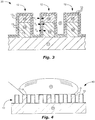
FIGs. 1-3 are schematic cross-sectional side views ofWGPs coating 13 located overribs 12, in accordance with embodiments of the present invention. The conformal-coating 13 inFIG. 1 includes a single layer - a distal conformal-coating 13d. The conformal-coating 13 inFIG. 2 includes two layers - a proximal conformal-coating 13p and a distal conformal-coating 13d. The conformal-coating 13 inFIG. 3 includes three layers - a proximal conformal-coating 13p, a middle conformal-coating 13m, and a distal conformal-coating 13d. -
FIG. 4 is a schematic cross-sectional side view of a WGP 40 with a conformal-coating 13, including a hydrophobic-layer, designed to keepwater 41, on a surface of theribs 12, in a Cassie-Baxter state, in accordance with an embodiment of the present invention. -
FIG. 5 is a schematic cross-sectional side view of aWGP 10 with array ofribs 12 located over a surface of atransparent substrate 11, in accordance with an embodiment of the present invention. Each of theribs 12 can includedifferent regions coating 55 with one chemistry can adhere to oneregion 15 and a conformal-coating 54 with a different chemistry can adhere to adifferent region 14. -
FIG. 6 is a schematic perspective-view of a WGP in accordance with an embodiment of the present invention. -
FIG. 7 is a graphical plot of the relationship between wavelength and reflectance of one polarization (Rs) in: (1) a WGP that includes germanium, in accordance with an embodiment of the present invention; and (2) WGPs that include silicon, in accordance with the prior-art. -
FIGs. 8-9 are schematic views ofimage projectors WGPs 84, in accordance with embodiments of the present invention. -
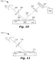
FIG. 10 shows an integrated circuit (IC)inspection tool 100 including a WGP 104, in accordance with embodiments of the present invention. -
FIG. 11 shows a flat panel display (FPD)manufacturing tool 110 including a WGP 114, in accordance with an embodiment of the present invention. - As used herein, "alkyl" refers to a branched, unbranched, or cyclic saturated hydrocarbon group. Alkyls include, but are not limited to, methyl, ethyl, n-propyl, isopropyl, n-butyl, isobutyl, t-butyl, octyl, and decyl, for example, as well as cycloalkyl groups such as cyclopentyl, and cyclohexyl, for example. The "alkyl" can typically be relatively small to facilitate vapor deposition, if overall atomic weight of the molecule is considered, such as for example ≤ 2 carbon atoms in one aspect, ≤ 3 carbon atoms in another aspect, ≤ 5 carbon atoms in another aspect, or ≤ 10 carbon atoms in another aspect. As used herein, "substituted alkyl" refers to an alkyl substituted with one or more substituent groups. The term "heteroalkyl" refers to an alkyl in which at least one carbon atom is replaced with a heteroatom. If not otherwise indicated, the term "alkyl" includes unsubstituted alkyl, substituted alkyl, and heteroalkyl.
- As used herein, "aryl" refers to a group containing a single aromatic ring or multiple aromatic rings that are fused together, directly linked, or indirectly linked (such that the different aromatic rings are bound to a common group such as a methylene or ethylene moiety). Aryl groups include, for example, phenyl, naphthyl, anthryl, phenanthryl, biphenyl, diphenylether, diphenylamine, and benzophenone. The term "substituted aryl" refers to an aryl group comprising one or more substituent groups. The term "heteroaryl" refers to an aryl group in which at least one carbon atom is replaced with a heteroatom. If not otherwise indicated, the term "aryl" includes unsubstituted aryl, substituted aryl, and heteroaryl.
- As used herein, the phrase "bond to the ribs" or similar phrases (e.g. "Z is a bond to the ribs") can mean a direct bond between the chemical and the ribs or a bond to an intermediate layer which is bonded directly, or through other layer(s) to the ribs. Thus, these layer(s) can be other conformal-coating(s).
- As used herein, the term "carbon chain" means a chain of carbon atoms linked together, including at least three carbon atoms in a row (e.g. -C-C-C-, - C=C-C-, etc.). The term carbon chain can include at least five carbon atoms in a row in one aspect, at least ten carbon atoms in a row in another aspect, or at least fifteen carbon atoms in a row in another aspect. The term carbon chain can also include ether linkages (C-O-C moieties). The term carbon chain includes single, double, and triple carbon to carbon bonds. The carbon atoms can be attached to any element or molecule.
- The term "elongated" means that a length L (see
FIG. 6 ) of theribs 12 is substantially greater than rib width W12 or rib thickness T12 (seeFIG. 1 ). For example, WGPs for ultraviolet or visible light can often have a rib width W12 between 20 and 100 nanometers and rib thickness T12 between 50 and 500 nanometers; and rib length L of about 1 millimeter to 20 centimeters or more, depending on the application. Thus,elongated ribs 12 can have a length L that is many times (even thousands of times) larger than rib width W12 or rib thickness T12. - As used herein, the term "gap" means a space, opening, or divide, separating one rib from another rib. The gap can be filled with a vacuum, gas, liquid, or solid, unless otherwise specified.
- As used herein, the unit "sccm" means cubic centimeters per minute at 0 °C and 1 atmosphere pressure.
- As used herein, the term "substrate" includes a base material, such as for example a glass wafer. The term "substrate" includes a single material, and also includes multiple materials (e.g. layered, composite, or the like), such as for example a glass wafer with at least one thin film on a surface of the wafer used together as the base material.
- Many materials used in optical structures absorb some light, reflect some light, and transmit some light. The following definitions are intended to distinguish between materials or structures that are primarily absorptive, primarily reflective, or primarily transparent. Each material can be primarily absorptive, primarily reflective, or primarily transparent in a specific wavelength of interest (e.g. all or a portion of the ultraviolet, visible, or infrared spectrums of light) and can have a different property in a different wavelength of interest.
- 1. As used herein, the term "absorptive" means substantially absorptive of light in the wavelength of interest.
- a. Whether a material is "absorptive" is relative to other materials used in the polarizer. Thus, an absorptive structure will absorb substantially more than a reflective or a transparent structure.
- b. Whether a material is "absorptive" is dependent on the wavelength of interest. A material can be absorptive in one wavelength range but not in another.
- c. In one aspect, an absorptive structure can absorb greater than 40% and reflect less than 60% of light in the wavelength of interest (assuming the absorptive structure is an optically thick film - i.e. greater than the skin depth thickness).
- d. In another aspect, an absorptive material can have a high extinction coefficient (k), relative to a transparent material, such as for example greater than 0.01 in one aspect or greater than 1.0 in another aspect.
- e. Absorptive ribs can be used for selectively absorbing one polarization of light.
- 2. As used herein, the term "reflective" means substantially reflective of light in the wavelength of interest.
- a. Whether a material is "reflective" is relative to other materials used in the polarizer. Thus, a reflective structure will reflect substantially more than an absorptive or a transparent structure.
- b. Whether a material is "reflective" is dependent on the wavelength of interest. A material can be reflective in one wavelength range but not in another. Some wavelength ranges can effectively utilize highly reflective materials. At other wavelength ranges, especially lower wavelengths where material degradation is more likely to occur, the choice of materials may be more limited and an optical designer may need to accept materials with a lower reflectance than desired.
- c. In one aspect, a reflective structure can reflect greater than 80% and absorb less than 20% of light in the wavelength of interest (assuming the reflective structure is an optically thick film - i.e. greater than the skin depth thickness).
- d. Metals are often used as reflective materials.
- e. Reflective wires can be used for separating one polarization of light from an opposite polarization of light.
- 3. As used herein, the term "transparent" means substantially transparent to light in the wavelength of interest.
- a. Whether a material is "transparent" is relative to other materials used in the polarizer. Thus, a transparent structure will transmit substantially more than an absorptive or a reflective structure.
- b. Whether a material is "transparent" is dependent on the wavelength of interest. A material can be transparent in one wavelength range but not in another.
- c. In one aspect, a transparent structure can transmit greater than 90% and absorb less than 10% of light at the wavelength of interest or wavelength range of use, ignoring Fresnel reflection losses.
- d. In another aspect, a transparent structure can have an extinction coefficient (k) of less than 0.01, less than 0.001, or less than 0.0001 in another aspect, at the wavelength of interest or wavelength range of use.
- 4. As used in these definitions, the term "material" refers to the overall material of a particular structure. Thus, a structure that is "absorptive" is made of a material that as a whole is substantially absorptive, even though the material may include some reflective or transparent components. Thus for example, a rib made of a sufficient amount of absorptive material so that it substantially absorbs light is an absorptive rib even though the rib may include some reflective or transparent material embedded therein.
- As illustrated in
FIGs. 1-6 , wire grid polarizers (WGPs or WGP for singular) 10, 20, 30, 40, 50, and 60 are shown comprisingribs 12 located over a surface of atransparent substrate 11. Theribs 12 can be elongated and arranged in a substantially parallel array. In some embodiments, theribs 12 can have a small pitch P (seeFIG. 1 ), such as for example a pitch P of less than 200 nanometers in one aspect or less than 150 nanometers in another aspect. - There can be gaps G between at least a portion of the ribs 12 (i.e. a gap G between a
rib 12 and an adjacent rib 12). The gaps G can be filled with air in one aspect, a liquid in another aspect, a transparent, solid, dielectric material in another aspect, or combinations thereof. - As shown in
FIGs. 1-5 , a conformal-coating 13 can be located over theribs 12. The conformal-coating 13 can also be located over an exposed surface of the substrate 11 ("exposed surface" meaning a surface of the substrate not covered with ribs 12). Use of a conformal-coating 13 can be beneficial because by following a contour of theribs 12 and an exposed surface of thesubstrate 11, conformal-coating thickness Tp, Tm, and Td, can be minimized, thus reducing any detrimental effect of the conformal-coating(s) 13 on WGP performance. The conformal-coating 13 can cover an exposed surface of theribs 12. The conformal-coating 13 can include a barrier-layer, a hydrophobic-layer, or both. The barrier-layer can include an oxidation-barrier, a moisture-barrier, or both. - The conformal-
coating 13 can include a single layer (FIG. 1 ) or multiple, different layers (seeFIGs. 2-3 ) across all or substantially all of theribs 12. The conformal-coating 13 can include at least one of: a proximal conformal-coating 13p, a middle conformal-coating 13m, and a distal conformal-coating 13d. It can be important to have sufficient thickness Tp, Tm, and Td for each of theselayers coating 13, in order to provide sufficient protection to theribs 12 and/or to provide a base for an upper layer of the conformal-coating 13. Thus, one or more of the proximal conformal-coating 13p, the middle conformal-coating 13m, and the distal conformal-coating 13d can have a thickness Tp, Tm, or Td that is at least 0.1 in one aspect, at least 0.5 nanometers in another aspect, or at least 1 nanometer in another aspect. - It can be important to have a sufficiently small thickness Tp, Tm, and Td for each of these
layers coating 13, in order to avoid or minimize degradation of WGP performance caused by the conformal-coating 13. Thus, one or more of the proximal conformal-coating 13p, the middle conformal-coating 13m, and the distal conformal-coating 13d can have a thickness Tp, Tm, or Td that is less than 2 nanometers in one aspect, less than 3 nanometers in another aspect, less than 5 nanometers in another aspect, less than 10 nanometers in another aspect, less than 15 nanometers in another aspect, or less than 20 nanometers in another aspect. - These thickness values can be a minimum thickness or a maximum thickness at any location of the conformal-
coating 13, or simply a thickness at a location of the conformal-coating 13. Each layer of the conformal-coating 13 can be a monolayer. - Alternatively, as shown in
FIG. 5 , a conformal-coating 55 with one chemistry can adhere to oneregion 15 and a conformal-coating 54 with a different chemistry can adhere to adifferent region 14. The chemistry of multiple, different, conformal-coatings can be selected such that different regions of the WGP, with different chemistries, can be protected. - The conformal-
coating 13 can include a hydrophobic-layer. The hydrophobic-layer can include a phosphonate conformal-coating, which can include:
ribs 12, such as but not limited to -CI, -OR6, -OCOR6, or -OH. Each R6 can independently be an alkyl group, an aryl group, or combinations thereof. - The hydrophobic-layer can alternatively or in addition include a silane conformal-coating, which can include chemical formula (1), chemical formula (2), or combinations thereof:

- Each R3 can be independently selected from the group consisting of: a silane-reactive-group, -H, R1, and R6. R6 was defined above. Each silane-reactive-group can be independently selected from the group consisting of: -CI, - OR6, -OCOR6, -N(R6)2, and -OH.
- R3 and/or R5 can be a small group, such as for example -OCH3, to allow easier vapor-deposition. Benefits of vapor-deposition are described below.
- The hydrophobic-layer can alternatively or in addition include a sulfur conformal-coating, which can include:

- As shown in
FIGs. 1-3 , eachrib 12 can includedifferent regions rib 15 and a lower-rib 14. The lower-rib 14 can be sandwiched between the upper-rib 15 and thesubstrate 11. At least one of these (lower-rib 14 or upper-rib 15) can be reflective (e.g. aluminum for visible light) and can be called a wire. At least one of these (lower-rib 14 or upper-rib 15) can be absorptive or transparent and can be called a rod. For example, for a selectively-absorptive WGP, with light incident from therib 12 side, the rod can be absorptive and can be the upper-rib 15, and the wire can be the lower-rib 14. SeeUS 7,961,393 which is incorporated by reference herein. - It can be difficult to protect both the rod and the wire, because protective chemistry that adheres well for one might not adhere well to the other. At least two of the silane conformal-coating, the phosphonate conformal-coating, and the sulfur conformal-coating can be applied to the
ribs 12. One of these can preferentially adhere to the rod and the other can preferentially adhere to the wire, thus providing effective protection to both. Money can be saved by using the phosphonate chemistry and the silane chemistry instead of just the silane conformal-coating because the phosphonate chemistry is presently less expensive than the silane chemistry. Thus, by combining the silane with the phosphonate, less of the expensive silane chemistry is needed. For example, the rod can be the upper-rib 15, can be made of silicon, and the silane conformal-coating 55 can preferentially adhere to the silicon upper-rib 15; and the wire can be the lower-rib 15, can be made of aluminum, and the phosphonate conformal-coating 54 can preferentially adhere to the aluminum lower-rib 15. - X can be a bond to the rod. For example, X can be -O-Si. T and/or Z can be a bond to the wire. For example, T and/or Z can be -O-Metal, where Metal is a metal atom. Thus, the silane conformal-coating can preferentially attach to one material (e.g. silicon) and the phosphonate conformal-coating or the sulfur conformal-coating can preferentially attach to another material (e.g. a metal) to provide protection to
multiple rib 12 materials. - It can be beneficial if the chemicals in the hydrophobic-layer include molecules that each has multiple bonds T, Z, and/or X to the
ribs 12. By each molecule forming multiple bonds X, more of the underlying surface (e.g. rib 12, proximal conformal-coating 13p, or middle conformal-coating 13m) can be bound and thus unavailable for bonding or interaction with undesirable chemicals, such as water for example. Also, multiple bonds to the surface can improve resiliency of the hydrophobic-layer because it can be less likely for multiple bonds Z/X/T to fail than for a single bond Z/X/T to fail. - Thus, R1 can be:


- For example, for g=2, the phosphonate conformal-coating, and moiety (3), the resulting chemical formula can be:

- Another way for molecules in the hydrophobic-layer to form multiple bonds Z, and/or X to the
ribs 12 is for R5 to be Z and/or for R3 to be X. This can be accomplished if, in the phosphonate chemistry as applied, R5 is a phosphonate-reactive-group and/or if, in the silane chemistry as applied, R3 is a silane-reactive-group. - The hydrophobic group can be or can include a carbon chain in one aspect and can include at least one halogen bonded to a carbon in another aspect. The carbon chain can include a perfluorinated group including at least 1 carbon atom in one aspect or at least 3 carbon atoms in another aspect. The perfluorinated group can include less than 20 carbon atoms in another aspect, less than 30 carbon atoms in another aspect, or less than 40 carbon atoms in another aspect. It can be beneficial for the perfluorinated group to have at least 4 carbon atoms to provide a hydrophobic chain. It can be beneficial for the perfluorinated group to not be too long or have too many carbon atoms in order to maintain a high enough vapor pressure to allow vapor-deposition.
- For example, the carbon chain of R1 can include CF3(CF2)n. Due to the high electronegativity of fluorine, it can be beneficial to have a hydrocarbon chain to separate the perfluorinated group from the phosphorous or sulfur. Thus, the carbon chain of R1 can include CF3(CF2)n(CH2)m, where n can be an integer within the boundaries of 0 ≤ n ≤ 20 in one aspect or 4 ≤ n ≤ 10 in another aspect, and m can be an integer within the boundaries of 0 ≤ m ≤ 5 in one aspect or 2 ≤ m ≤ 5 in another aspect.
- In order to allow vapor-deposition, it can be important for some or all of the conformal-coating chemistry to have a relatively lower molecular weight, but it can also be important for the carbon chain to be long enough to provide sufficient hydrophobicity. Thus, each molecule in the phosphonate conformal-coating (excluding the bond to the ribs Z), each molecule in the silane conformal-coating (excluding the bond to the ribs X), and/or each molecule in the sulfur conformal-coating (excluding the bond to the ribs T), can have a molecular weight of at least 100 grams per mole in one aspect, at least 150 grams per mole in another aspect, or at least 400 grams per mole in another aspect, and less than 600 grams per mole in one aspect, less than 1000 grams per mole in another aspect, or less than 1500 grams per mole in another aspect.
- In the hydrophobic-layer, it can be important to have a strong bond between silicon (Si) and R1, between phosphorous (P) and R1, and/or between sulfur (S) and R1, to avoid the R1 group breaking away from Si, P, or S. Thus, the bond between silicon (Si) and R1 can be a silicon to carbon bond (Si-C); the bond between phosphorous (P) and R1 can be a phosphorous to carbon bond (P-C); and/or the bond between sulfur (S) and R1 can be a sulfur to carbon bond (S-C).
- The hydrophobic-layer located on the
ribs 12 can provide a hydrophobic surface, which can be a superhydrophobic surface, depending on the chemistry and the structure of the ribs, such as pitch P and rib width W12. As shown inFIG. 4 , the WGP and conformal-coating 13 can include a hydrophobic-layer and can be capable of keepingwater 41, on a surface of theribs 12, in a Cassie-Baxter state. Having water on theWGP 10 in a Cassie-Baxter state can be beneficial because thewater 41 does not substantially enter or remain in the gaps G, thus avoiding or reducing corrosion on sides of theribs 12 and avoiding or reducing toppling of theribs 12 due to water's tensile forces. Also, if thewater 41 is in a Cassie-Baxter state, the water can more easily roll off the surface of the WGP, often carrying dust particles with it. A water contact angle A can be greater than 110° in one aspect, greater than 120° in another aspect, greater than 130° in another aspect, or greater than 140° in another aspect. - As described above, at least one of the lower-
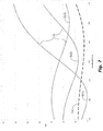
rib 14 or upper-rib 15 can be reflective (e.g. aluminum for visible light) and can be called a wire and at least one can be absorptive or transparent and can be called a rod. The rod can be made of silicon, an absorptive material for visible light. Silicon-containing, selectively-absorptive WGPs have been used in image projectors. Selectively-absorptive WGPs can substantially allow one polarization (e.g. p-polarized light) to pass through and can absorb an opposite polarization (e.g. s-polarized light). In an image projector, the p-polarized light can be used for forming the image. Ghosting of the projected image can be reduced by the WGP absorbing the s-polarized light. Some image projectors separate light into three different light beams. One of these light beams can have a wavelength of about 450 nm, another can have a wavelength of about 550 nm, and the third can have a wavelength of about 650 nm. In order to optimize polarization of each light beam, different WGP designs can be used for each different light beam. - Graphical silicon-plots Si in
FIG. 7 show the relationship between wavelength and reflectance of one polarization (e.g. reflectance of s-polarization Rs) of a selectively-absorptive WGP that includes silicon. The first silicon-plot Si(1) is for with a WGP having a silicon thickness selected for optimal (low) Rs at around 450 nanometers. The second silicon-plot Si(2) is for with a WGP having a silicon thickness selected for optimal (low) Rs at around 550 nanometers. The third silicon-plot Si(3) is for with a WGP having a silicon thickness selected for optimal (low) Rs at around 650 nanometers. It would be simpler, and manufacturing errors could be avoided, if less than three different WGP designs were required. - Also shown in
FIG. 7 is a graphical germanium-plot Ge of the relationship between wavelength and reflectance of one polarization (e.g. s-polarization) of a selectively-absorptive WGP that includes germanium. The WGP that includes germanium has better Rs across 2/3 of wavelengths from 400-700 nm. Thus, use of a WGP that includes germanium can provide a benefit of improved Rs from about 500-700 nm. Another possible benefit is that, due to the flatness of the germanium-plot Ge, one WGP design can be used for at least two of the light beams (e.g. 550 and 650). - Another disadvantage of a selectively-absorptive WGP that includes silicon is that Rs tends to increase (worsen) over time, which can result in gradually deteriorating image-projection quality over time. Selectively-absorptive WGPs that include germanium, however, show the opposite --- Rs decreases (improves) over time, thus avoiding deteriorating image-projection quality over time. Due to the reasonably good initial Rs across the entire visible spectrum, and decreasing Rs over time, a single selectively-absorptive WGP that includes germanium can be used across the entire visible spectrum.
- In one embodiment, a rod in a selectively-absorptive WGP can include at germanium. For example, the rod can include at least 20 mass percent germanium in one aspect, at least 50 mass percent germanium in another aspect, at least 80 mass percent germanium in another aspect, or at least 95 mass percent germanium in another aspect.
- A difficulty of using germanium, however, is that it has a soluble oxide (about 4.5 g/L at 25°C). WGP performance can decrease if the polarizer, with an exterior of the
rib 12 including germanium / germanium oxide, is immersed into an aqueous solution. Such aqueous solution can be for applying a protective coating (e.g. amino phosphonate as taught inU.S. Patent Number 6,785,050 which is incorporated herein by reference). Such protective coatings can be important to avoid corrosion of the WGP. - Other desirable WGP materials can have the same problem as germanium and their performance can degrade by immersing in an aqueous solution. WGPs made with such water-soluble materials can also benefit from anhydrous-immersion and / or vapor-deposition for applying the conformal-coating(s) 13. For example, an anhydrous method can be helpful if a material of an exterior of the
ribs 12 has solubility in water of at least 0.015 grams per liter at 25°C in one aspect, at least 0.02 grams per liter at 25°C in another aspect, at least 0.05 grams per liter at 25°C in another aspect, at least 0.5 grams per liter at 25°C in another aspect, at least 1 gram per liter at 25°C in another aspect, at least 2 grams per liter at 25°C in another aspect, or at least 4 grams per liter at 25°C in another aspect. - Thus, at least for WGPs with materials that are soluble in water, it can be beneficial to have an anhydrous method for applying protective coatings, such as anhydrous-immersion or vapor-deposition. Non-limiting examples of vapor-deposition methods include chemical vapor-deposition (CVD), low-pressure CVD (LPCVD), plasma-enhanced CVD, physical vapor-deposition (PVD), atomic layer deposition (ALD), thermoreactive diffusion, electron-beam deposition, sputtering, and thermal evaporation. Anhydrous-immersion can include submersion of the WGP in an anhydrous, liquid bath. A solvent that will not dissolve
rib 12 materials can be selected. Vapor-deposition can be preferred over immersion because of reduced process-waste disposal problems, reduced health hazards, reduced or no undesirable residue from rinsing, and vapor-deposition can be done with standard semiconductor processing equipment. - The oxidation-barrier and the moisture-barrier described below can be applied by ALD. Some embodiments of the hydrophobic-layer have a sufficiently-high vapor pressure and can be applied by vapor-deposition.
- The conformal-
coating 13 can include a barrier-layer. The barrier-layer can include an oxidation-barrier, a moisture-barrier, or both. The barrier-layer can include a metal oxide, or layers of different metal oxides. - Oxidation of
WGP ribs 12 can degrade performance of the WGP, by adversely affecting contrast or Rs. An oxidation-barrier can reduce oxidation of theribs 12, and thus reduce or avoid such WGP performance degradation. The term "oxidation-barrier" means a first material capable of reducing the ingress of oxygen into a second material, which may cause the second material to oxidize. An oxidation barrier can be placed on theribs 12 to protect theribs 12 from oxidation. Non-limiting examples of chemicals that can be used as an oxidation-barrier include: aluminum oxide, silicon oxide, silicon nitride, silicon oxynitride, silicon carbide, or combinations thereof. - WGP corrosion can degrade WGP performance. For example, water can condense onto the WGP and wick into narrow channels between ribs due to capillary action. The water can then corrode the ribs. Corroded regions can have reduced contrast, changed Rs, or can fail to polarize at all. A moisture-barrier can resist corrosion. A moisture-barrier can protect the
ribs 12 from water or other corrosion. Examples of chemicals that can be used as a moisture-barrier include: hafnium oxide, zirconium oxide, or combinations thereof. - The barrier-layer can include rare earth oxides, for example, oxides of scandium, yttrium, lanthanum, cerium, praseodymium, neodymium, promethium, samarium, europium, gadolinium, terbium, dysprosium, holmium, erbium, thulium, ytterbium, and lutetium. These rare earth oxides can be at least part of the oxidation-barrier, the moisture-barrier, or both.
- The barrier-layer can be distinct from the
ribs 12, meaning (1) there can be a boundary line or layer between theribs 12 and the barrier-layer; or (2) there can be some difference of material of the barrier-layer relative to a material of theribs 12. For example, a native aluminum oxide can form at a surface ofaluminum ribs 12. A layer of aluminum oxide (oxidation-barrier) can then be applied to the ribs (e.g. by ALD). This added layer of aluminum oxide can be important, because a thickness and / or density of the native aluminum oxide can be insufficient for protecting a core of the ribs 12 (e.g. substantially pure aluminum) from oxidizing. In this example, although the oxidation-barrier (Al2O3) has the same material composition as a surface (Al2O3) of theribs 12, the oxidation-barrier can still be distinct due to (1) a boundary layer between the oxidation-barrier and theribs 12 and / or (2) a difference in material properties, such as an increased density of the oxidation-barrier relative to the native aluminum oxide. - A silicon dioxide conformal-coating can be located between the silane conformal-coating and the
ribs 12. The silicon dioxide conformal-coating can help the silane conformal-coating 14 bond to theribs 12. The silicon dioxide conformal-coating can be the proximal conformal-coating 13p or the middle conformal-coating 13m, or an additional layer of the conformal-coating 13 located between the middle conformal-coating 13m and the distal conformal-coating 13d. - The oxidation-barrier can be less effective at resisting corrosion. The moisture-barrier and / or hydrophobic-layer can be less effective at resisting oxidation. Thus, it can be beneficial to combine both an oxidation-barrier with a moisture-barrier and / or hydrophobic-layer.
- Although the moisture-barrier can resist corrosion, it can eventually break down. Thus, it can be beneficial to minimize exposure of the moisture-barrier to water. A hydrophobic-layer can minimize or prevent condensed water on the WGP from attacking the moisture-barrier, thus extending the life of the moisture-barrier and the WGP. If the hydrophobic-layer perfectly covers the
ribs 12, and never breaks down, then a moisture-barrier might not be needed. But, due to imperfections in manufacturing, there can be locations on theribs 12 that are not covered, or less densely covered, by the hydrophobic-layer. The moisture-barrier can provide protection to these locations. Also, the hydrophobic-layer can break down over time. The moisture-barrier can provide protection after such breakdown. Therefore, it can be beneficial to combine both a moisture-barrier and a hydrophobic-layer. - If the hydrophobic-layer keeps water on the
ribs 12 in a Cassie-Baxter state, thenrib 12 damage, which could otherwise be caused by tensile forces in water in the gaps G, can be avoided. Also, the water can roll off the surface of the WGP, often carrying dust particles with it, in a self-cleaning fashion. These are added benefits of the hydrophobic-layer that might not be provided by the oxidation-barrier or the moisture-barrier. - Thus, it can be beneficial for improved WGP protection and/or for improved adhesion of an upper-layer of the conformal-
coating 13, for the conformal-coating 13 to have multiple layers, which can include at least two of: an oxidation-barrier, a moisture-barrier, a silicon dioxide conformal-coating, and a hydrophobic-layer. This added protection, however, is not free. Each additional layer in the conformal-coating 13 can increase WGP cost, especially if more than one tool is required to apply the multiple layers of the conformal-coating 13. Thus, a determination of the number of layers in the conformal-coatings 13 can be made by weighing cost against desired protection. -
WGP 10 inFIG. 1 includes a conformal-coating 13 with one layer: a distal conformal-coating 13d. The distal conformal-coating 13d can be the oxidation-barrier, the moisture-barrier, or the hydrophobic-layer. -
WGP 20 inFIG. 2 includes a conformal-coating 13 with two layers: a proximal conformal-coating 13p located closer to theribs 12 andsubstrate 11 and a distal conformal-coating 13d located over the proximal conformal-coating 13p. The proximal conformal-coating 13p and the distal conformal-coating 13d can comprise oxidation-barrier(s), moisture-barrier(s), and / or hydrophobic-layer(s). -
WGP 30 inFIG. 3 includes a conformal-coating 13 with three layers: the proximal conformal-coating 13p, the distal conformal-coating 13d, and a middle conformal-coating 13m located between the proximal conformal-coating 13p and the distal conformal-coating 13d. The proximal conformal-coating 13p, the middle conformal-coating 13m, and the distal conformal-coating 13d can comprise oxidation-barrier(s), moisture-barrier(s), and / or hydrophobic-layer(s). Although not shown in the figures, there can be more than three layers in the conformal-coating 13. - It can be beneficial to use the moisture-barrier over the oxidation-barrier (i.e. the oxidation-barrier is proximal and the moisture-barrier is distal or middle), thus the moisture-barrier can provide corrosion protection to the oxidation-barrier. The oxidation-barrier can provide a good substrate for deposition of the moisture-barrier, resulting in a less porous moisture-barrier. Thus, the same moisture protection may be obtained by a relatively thinner moisture-barrier. This can be important because the moisture-barrier can degrade WGP performance, but such degradation can be minimized by reduced moisture-barrier thickness. Furthermore, the moisture-barrier can provide an improved surface for attachment of the hydrophobic-layer (if used).
- It can be beneficial for the hydrophobic-layer to be located over the barrier-layer (i.e. the hydrophobic-layer can be the distal conformal-coating 13d) in order to best keep moisture from entering the gaps G and to minimize or eliminate moisture exposure of the underlying layer(s) in the conformal-coating 13 (e.g. the proximal conformal-
coating 13p and also possibly the middle conformal-coating 13m). - The WGPs described herein can be used in an image projector.
Image projector 80, as shown inFIG. 8 , can comprise alight source 81, color-splittingoptics 82, color-combiningoptics 88, aprojection lens system 85, one or more spatiallight modulators 87, and one ormore WGPs 84. - The
light source 81 can emit a beam oflight 83, which can initially be unpolarized. The color-splittingoptics 82 can be located to receive at least part of the beam oflight 83 and can split the beam of light 83 into multiple, differently-colored light beams (colored beams) 83c. The colored beams 83c can be primary colors. - Color-combining
optics 88 can be located to receive and can recombine at least some of the colored beams 83c into a combined beam orfinal beam 83f. Color-combiningoptics 88 are sometimes called X-Cubes, X-Cube prisms, X-prisms, light recombination prisms, or cross dichroic prisms. Color-combiningoptics 88 are used in computer projectors for combining different colors of light into a single image to be projected. X-Cubes are typically made of four right angle prisms, with dichroic coatings, that are cemented together to form a cube. - The
projection lens system 85 can be located to receive the combinedbeam 83f and can project acolored image 83i onto ascreen 86. Although other projection lens systems can be used, exemplaryprojection lens systems 85 are described inU.S. Patent Numbers 6,585,378 and6,447,120 , which are hereby incorporated herein by reference in their entirety. - One spatial
light modulator 87 can be located to receive, in each light path between the color-splittingoptics 82 and the color-combiningoptics 88, one of the colored beams 83c. Each spatiallight modulator 87 can have a plurality of pixels. Each pixel can receive a signal. The signal can be an electronic signal. Depending on whether or not each pixel receives the signal, the pixel can rotate a polarization of, or transmit or reflect without causing a change in polarization of, incident light. The spatial light modulator(s) 87 can be a liquid crystal device / display (LCD) and can be transmissive, reflective, or transflective. - Each
WGP 84, according to one of the WGP designs described herein, can be located in one of the colored beams 83c prior to entering the spatiallight modulator 87, after exiting the spatiallight modulator 87, or both. The WGP(s) 84 help form thecolored image 83i by transmitting, reflecting, or absorbing light of each pixel depending on the type ofWGP 84 and whether each pixel received the signal. - Another type of
image projector 90 is shown inFIG. 9 , and can comprise alight source 91, aprojection lens system 85, a spatiallight modulator 87, and aWGP 84. Thelight source 91 can sequentially emit multiple, differently-colored light beams (colored beams) 93. The colored beams 93 can be primary colors. Theprojection lens system 85 can be located to receive the colored beams 93 and can project acolored image 83i onto ascreen 86. Theprojection lens system 85, spatiallight modulator 87,WGP 84,colored image 83i, andscreen 86 were described above. - The spatial
light modulator 87 can be located to receive, in a light path between thelight source 91 and theprojection lens system 85, the colored beams 93. TheWGP 84 can be located in the colored beams 93 prior to entering the spatiallight modulator 87 and after exiting the spatiallight modulator 87. - Integrated circuits (ICs or IC) can be made of semiconductor material and can include nanometer-sized features. ICs can be used in various electronic devices (e.g. computer, motion sensor, etc.). Defects in the IC can cause the electronic device to fail. Thus, inspection of the IC can be important for avoiding failure of the electronic device, while in use by the consumer. Such inspection can be difficult due to the small feature-size of IC components. Light, with small wavelengths (e.g. ultraviolet), can be used to inspect small feature-size components. It can be difficult to have sufficient contrast between these small feature-size components and defects or their surroundings. Use of polarized light can improve integrated circuit (IC) inspection contrast. It can be difficult to polarize the small wavelengths of light (e.g. ultraviolet/UV) used for IC inspection. Polarizers that can polarize such small wavelengths, and that can withstand exposure to high-energy wavelengths of light, may be needed.
- The WGPs described herein can polarize small wavelengths of light (e.g. UV) and can be made of materials sufficiently durable to withstand exposure to such light. An
IC inspection tool 100 is shown inFIG. 10 , comprising alight source 101 and astage 102 for holding anIC wafer 103. Thelight source 101 can be located to emit an incident light-beam 105 (e.g. visible, ultraviolet, or x-ray) onto theIC wafer 103. The incident light-beam 105 can be directed to thewafer 103 by optics (e.g. mirrors). The incident light-beam 105 can have an acute angle ofincidence 109 with a face of thewafer 103. To improve inspection contrast, a WGP 104 (according to an embodiment described herein) can be located in, and can polarize, the incident light-beam 105. - A detector 107 (e.g. CCD) can be located to receive an output light-
beam 106 from theIC wafer 103. Anelectronic circuit 108 can be configured to receive and analyze a signal from the detector 107 (the signal based on the output light-beam 106 received by the detector 107). To improve inspection contrast, a WGP 104 (according to an embodiment described herein) can be located in, and can polarize, the output light-beam 106. - The WGPs described herein can be used in the manufacture of flat panel displays (FPDs for plural or FPD for singular). FPDs can include an aligned polymer film and liquid crystal. An
FPD manufacturing tool 110 is shown inFIG. 11 , comprising alight source 111, astage 112 for holding anFPD 113, and a WGP 114 (according to an embodiment described herein). Thelight source 111 can emitultraviolet light 115. TheWGP 114 can be located between thelight source 111 and thestage 112 and can polarize theultraviolet light 115. Exposing theFPD 113 to polarized ultraviolet light 115 can align the polymer film. SeeUS Patents 8,797,643 and8,654,289 , both incorporated herein by reference. Exposing theFPD 113 to polarized ultraviolet light 115 can help repair theFPD 113. SeeUS Patent 7,697,108 , which is incorporated herein by reference. - A method of making a WGP can include some or all of the following steps. The steps can be performed in the order shown, or alternate order:
- 1. Obtaining
ribs 12 located over a surface of atransparent substrate 11. Theribs 12 and thetransparent substrate 11 can have properties as described above. There can be gaps G between at least a portion of theribs 12. SeeFIG. 6 . - 2. Exposing the WGP to ultraviolet light and/or ozone:
- a. This step may be done before applying one or more of the following: a proximal conformal-
coating 13p, a middle conformal-coating 13m, and a distal conformal-coating 13d. - b. Exposing the WGP to ultraviolet light and ozone can be done sequentially or simultaneously.
- c. A duration of this step can be less than two minutes in one aspect or less than 20 minutes in another aspect.
- a. This step may be done before applying one or more of the following: a proximal conformal-
- 3. Applying a proximal conformal-
coating 13p. SeeFIGs. 2-3 . - 4. Applying a middle conformal-
coating 13m. SeeFIG. 3 . - 5. Plasma cleaning the WGP.
- a. Plasma cleaning can generate more reactive groups on the surface (i.e. surface of the
ribs 12, proximal conformal-coating 13p, or middle conformal-coating 13m), thus improving bonding of the distal conformal-coating 13d. - b. Non-limiting examples of plasmas include O2, H2, Ar, and N2.
- c. Plasma cleaning can be performed at various temperatures, such as for example between 140 °C and 200 °C.
- d. One plasma, used for cleaning the WGP, included O2 (flow
rate 15 sccm) and H2 (flowrate 10 sccm) at a power of 400 W for 5 minutes at a temperature of 160 °C.
- a. Plasma cleaning can generate more reactive groups on the surface (i.e. surface of the
- 6. Exposing the WGP to a gas.
- a. The gas can include water vapor. The water vapor can have a pressure of less than 100 Torr.
- b. This step can increase the number of hydroxyl groups on the underlying surface (
e.g. ribs 12, proximal conformal-coating 13p, or middle conformal-coating 13m), which can improve bonding of phosphonate of the hydrophobic-layer. - c. Duration, pressure, and temperature of this step may need to be carefully limited, depending on the rib structure and the nature of the underlying surface, in order to avoid corrosion.
- 7. Applying a distal conformal-
coating 13d. - 8. Baking the WGP. Baking can improve bonding of the hydrophobic-layer.
- a. Baking temperature examples: The WGP can be baked at greater than between 100 °C in one aspect, greater than 130 °C in another aspect, or greater than 150 °C in another aspect; and less than 300 °C in one aspect, less than 320 °C in another aspect, or less than 400 °C in another aspect.
- b. Baking time examples: The WGP can be baked for at least 5 minutes, at least 10 minutes in another aspect; and less than 60 minutes in one aspect or less than 90 minutes in another aspect.
- c. Baking at 150 °C for 15 minutes has been successful.
- One, two, or every layer of the conformal coating (the proximal conformal-
coating 13p, the middle conformal-coating 13m, and/or the distal conformal-coating 13d) can have one or more of the following characteristics: - 1. can cover the underlying layer, e.g. an exposed surface of the
ribs 12, the proximal conformal-coating 13p, or middle conformal-coating 13p; - 2. can be applied by atomic layer deposition, vapor-deposition, or other anhydrous deposition method;
- 3. can be applied at an elevated temperature, such as for example at least 300°C in one aspect, at least 350°C in another aspect, at least 400°C in another aspect; and less than 500°C in one aspect or less than 600°C in another aspect;
- 4. can include a metal oxide;
- 5. can include hafnium oxide, zirconium oxide, aluminum oxide, silicon oxide, silicon nitride, silicon oxynitride, a rare earth oxide, or combinations thereof.
- 6. can be applied by exposing the WGP to a chemical, the chemical including Si(R1)d(R2)e(R3)g, (R1)iPO(R4)j(R5)k, or combinations thereof, where:
- a. d is 1, 2, or 3, e is 1, 2, or 3, g is 0, 1, or 2, and d+e+g = 4;
- b. i is 1 or 2, j is 1 or 2, k is 0 or 1, and i+j+k = 3;
- c. each R1 is independently a hydrophobic group;
- d. R2 is a silane-reactive-group;
- e. each silane-reactive-group is independently selected from: -CI, -OR6, - OCOR6, -N(R6)2, and -OH;
- f. R4 is a phosphonate-reactive-group;
- g. each phosphonate-reactive-group is independently selected from: -Cl, -OR6, -OCOR6, and -OH; and
- h. each R6 is independently an alkyl group, an aryl group, or combinations thereof.
- The hydrophobic group, the phosphonate-reactive-group, the silane-reactive-group, R6, R3, and R5 can have the properties as described above. The silane chemical and the phosphonate chemical can be applied sequentially or simultaneously.
Claims (15)
- A wire grid polarizer (WGP) comprising:ribs located over a surface of a transparent substrate, wherein the ribs are elongated and arranged in an array;gaps between at least a portion of the ribs; anda conformal-coating located over the ribs, wherein the conformal-coating includes a barrier layer, the barrier layer including at least one of aluminum oxide, silicon oxide, silicon nitride, silicon oxynitride, silicon carbide, hafnium oxide, zirconium oxide, and a rare earth oxide.
- The WGP of claim 1, wherein the barrier-layer is distinct from the ribs.
- The WGP of claim 1, wherein a material of an exterior surface of the ribs has solubility in water of at least 0.015 grams per liter at 25°C.
- The WGP of claim 1, wherein a material of an exterior surface of the ribs includes germanium.
- The WGP of claim 1, wherein:the barrier-layer comprises two layers of different materials, including an oxidation-barrier and a moisture-barrier;the oxidation-barrier includes aluminum oxide, silicon oxide, silicon nitride, silicon oxynitride, silicon carbide, or combinations thereof;the moisture-barrier includes hafnium oxide, zirconium oxide, or combinations thereof; andthe oxidation-barrier is located between the moisture-barrier and the ribs.
- The WGP of claim 5, wherein the oxidation-barrier has a thickness of less than 5 nanometers and the moisture-barrier has a thickness of less than 5 nanometers.
- The WGP of claim 1, wherein:the conformal-coating further comprises a hydrophobic-layer located over the ribs;the barrier-layer is located between the hydrophobic-layer and the ribs; andthe hydrophobic-layer includes a phosphonate conformal-coating, wherein the phosphonate conformal-coating includes:

- The WGP of claim 7, wherein R5 is a phosphonate-reactive-group, R1, R6, or Z, and the phosphonate-reactive-group is -Cl, -OR6, -OCOR6, or -OH, R6 can independently be an alkyl group, an aryl group, or combinations thereof.
- The WGP of claim 7, wherein the hydrophobic-layer further comprises a silane conformal-coating and the silane conformal-coating includes chemical formula (1), chemical formula (2), or combinations thereof:
 r is a positive integer;X is a bond to the ribs;each R3 independently is a silane-reactive-group, -H, R1, R6, or X;each silane-reactive-group independently is -Cl, -OR6, -OCOR6, -N(R6)2, or -OH; andeach R6 independently is an alkyl group, an aryl group, or combinations thereof.
 - The WGP of claim 9, wherein each of the ribs includes a rod and a wire, the wire is reflective, the rod is absorptive, X is a bond to the rod, and Z is a bond to the wire.
- The WGP of claim 1, wherein:the conformal-coating further comprises a hydrophobic-layer located over the ribs;the barrier-layer is located between the hydrophobic-layer and the ribs; andthe hydrophobic-layer includes a silane conformal-coating and the silane conformal-coating includes chemical formula (1), chemical formula (2), or combinations thereof:

- A method of making a wire-grid polarizer, the method comprising:obtaining an array of ribs located over a surface of a transparent substrate, the ribs being elongated with gaps between at least a portion of the ribs; andapplying a barrier layer of a conformal-coating over the ribs by vapor deposition, the barrier layer including at least one of aluminum oxide, silicon oxide, silicon nitride, silicon oxynitride, silicon carbide, hafnium oxide, and zirconium oxide.
- The method of claim 12, further comprising applying a hydrophobic-layer of the conformal-coating by vapor deposition after applying the barrier layer, applying the hydrophobic-layer includes exposing the WGP to a chemical, the chemical including (R1)iPO(R4)j(R5)k, where:i is 1 or 2, j is 1 or 2, k is 0 or 1, and i+j+k = 3;each R1 independently is a hydrophobic group;R4 is a phosphonate-reactive-group;each phosphonate-reactive-group independently is -Cl, -OR6, -OCOR6, or - OH; andeach R6 independently is an alkyl group, an aryl group, or combinations thereof.
- The method of claim 12, further comprising applying a hydrophobic-layer of the conformal-coating by vapor deposition after applying the barrier layer, applying the hydrophobic-layer includes exposing the WGP to a chemical, the chemical including Si(R1)d(R2)e(R3)g, where:d is 1, 2, or 3, e is 1, 2, or 3, g is 0, 1, or 2, and d+e+g = 4;each R1 independently is a hydrophobic group;R2 is a silane-reactive-group;each silane-reactive-group independently is -Cl, -OR6, -OCOR6, -N(R6)2, or - OH; andeach R3 is any chemical element or group.
- The method of claim 12, wherein:applying the barrier layer includes applying an oxidation-barrier then applying a moisture-barrier;the oxidation-barrier includes aluminum oxide, silicon oxide, silicon nitride, silicon oxynitride, silicon carbide, or combinations thereof; andthe moisture-barrier includes hafnium oxide, zirconium oxide, or combinations thereof.
Applications Claiming Priority (8)
| Application Number | Priority Date | Filing Date | Title |
|---|---|---|---|
| US201562142854P | 2015-04-03 | 2015-04-03 | |
| US201562190188P | 2015-07-08 | 2015-07-08 | |
| US201562209024P | 2015-08-24 | 2015-08-24 | |
| US201562216782P | 2015-09-10 | 2015-09-10 | |
| US201562242883P | 2015-10-16 | 2015-10-16 | |
| US201562265773P | 2015-12-10 | 2015-12-10 | |
| US15/078,495 US10054717B2 (en) | 2015-04-03 | 2016-03-23 | Oxidation and moisture barrier layers for wire grid polarizer |
| PCT/US2016/024713 WO2016160803A1 (en) | 2015-04-03 | 2016-03-29 | Oxidation and moisture barrier layers for wire grid polarizer |
Publications (3)
| Publication Number | Publication Date |
|---|---|
| EP3237943A1 EP3237943A1 (en) | 2017-11-01 |
| EP3237943A4 EP3237943A4 (en) | 2018-07-04 |
| EP3237943B1 true EP3237943B1 (en) | 2021-01-13 |
Family
ID=57007562
Family Applications (1)
| Application Number | Title | Priority Date | Filing Date |
|---|---|---|---|
| EP16773995.2A Active EP3237943B1 (en) | 2015-04-03 | 2016-03-29 | Oxidation and moisture barrier layers for wire grid polarizer |
Country Status (6)
| Country | Link |
|---|---|
| US (1) | US10054717B2 (en) |
| EP (1) | EP3237943B1 (en) |
| JP (4) | JP7059497B2 (en) |
| KR (1) | KR20170134422A (en) |
| CN (2) | CN111766656A (en) |
| WO (1) | WO2016160803A1 (en) |
Families Citing this family (11)
| Publication number | Priority date | Publication date | Assignee | Title |
|---|---|---|---|---|
| KR102422109B1 (en) | 2015-01-08 | 2022-07-19 | 삼성디스플레이 주식회사 | Liquid crystal display and manufacturing method thereof |
| US10534120B2 (en) | 2015-04-03 | 2020-01-14 | Moxtek, Inc. | Wire grid polarizer with protected wires |
| US20160291227A1 (en) * | 2015-04-03 | 2016-10-06 | Moxtek, Inc. | Wire Grid Polarizer with Water-Soluble Materials |
| US10444410B2 (en) | 2016-08-16 | 2019-10-15 | Moxtek, Inc. | Overcoat wire grid polarizer having conformal coat layer with oxidation barrier and moisture barrier |
| CN109804281A (en) * | 2016-11-22 | 2019-05-24 | 莫克斯泰克公司 | Outer painting wire-grid polarizer |
| CN107102394B (en) * | 2017-07-03 | 2020-05-22 | 京东方科技集团股份有限公司 | Wire grid polarizer, manufacturing method thereof and display panel |
| JP2019061125A (en) * | 2017-09-27 | 2019-04-18 | デクセリアルズ株式会社 | Polarizer, manufacturing method for the same and optical equipment |
| JP6678630B2 (en) * | 2017-09-28 | 2020-04-08 | デクセリアルズ株式会社 | Polarizing plate and optical device having the same |
| US10852464B2 (en) * | 2018-03-01 | 2020-12-01 | Moxtek, Inc. | High-contrast polarizer |
| JP7333168B2 (en) * | 2018-11-19 | 2023-08-24 | デクセリアルズ株式会社 | POLARIZING ELEMENT, POLARIZING ELEMENT MANUFACTURING METHOD, AND OPTICAL DEVICE |
| US11746418B2 (en) * | 2018-12-03 | 2023-09-05 | Moxtek, Inc. | Chemical vapor deposition of thick inorganic coating on a polarizer |
Family Cites Families (65)
| Publication number | Priority date | Publication date | Assignee | Title |
|---|---|---|---|---|
| US3630790A (en) | 1969-05-13 | 1971-12-28 | Dow Chemical Co | Method of protection of metal surfaces from corrosion |
| US5045347A (en) | 1986-11-07 | 1991-09-03 | Hoechst Aktiengesellschaft | Reclaimable polyester film having adhesion-promoting coating |
| US4705725A (en) | 1986-11-28 | 1987-11-10 | E. I. Du Pont De Nemours And Company | Substrates with sterically-protected, stable, covalently-bonded organo-silane films |
| US4759611A (en) | 1986-12-19 | 1988-07-26 | Polaroid Corporation, Patent Department | Liquid crystal display having silylated light polarizers |
| DE4313130C1 (en) | 1993-04-22 | 1994-05-26 | Goldschmidt Ag Th | Silanes and organosilicon hydrides prodn. - by redn. of corresp. silicon halides with non-pyrophoric storage magnesium hydride in THF etc., with continuous removal of halide deposits |
| DE19539789A1 (en) * | 1995-10-26 | 1997-04-30 | Merck Patent Gmbh | Means and methods for producing water-repellent coatings on optical substrates |
| JP3520775B2 (en) | 1998-09-08 | 2004-04-19 | ソニーケミカル株式会社 | Low adhesion paint |
| US6447120B2 (en) | 1999-07-28 | 2002-09-10 | Moxtex | Image projection system with a polarizing beam splitter |
| US6585378B2 (en) | 2001-03-20 | 2003-07-01 | Eastman Kodak Company | Digital cinema projector |
| MXPA04007398A (en) | 2002-02-05 | 2005-06-20 | Gencell Corp | Silane coated metallic fuel cell components and methods of manufacture. |
| EP2031425A1 (en) | 2002-02-12 | 2009-03-04 | OC Oerlikon Balzers AG | Optical component comprising submicron hollow spaces |
| US6785050B2 (en) * | 2002-05-09 | 2004-08-31 | Moxtek, Inc. | Corrosion resistant wire-grid polarizer and method of fabrication |
| US7404878B2 (en) | 2003-03-31 | 2008-07-29 | Chlorine Engineers Corp., Ltd. | Gas diffusion electrode assembly, bonding method for gas diffusion electrodes, and electrolyzer comprising gas diffusion electrodes |
| US7189479B2 (en) * | 2003-08-21 | 2007-03-13 | 3M Innovative Properties Company | Phototool coating |
| US7961393B2 (en) | 2004-12-06 | 2011-06-14 | Moxtek, Inc. | Selectively absorptive wire-grid polarizer |
| US7674927B2 (en) | 2005-05-23 | 2010-03-09 | Innovation Chemical Technologies, Ltd | Fluorinated organic silicon coating material |
| KR100720454B1 (en) | 2005-06-14 | 2007-05-22 | 엘지.필립스 엘시디 주식회사 | Liquid Crystal Display Device, and method of fabricating the same |
| US7345855B2 (en) * | 2005-09-07 | 2008-03-18 | International Business Machines Corporation | Tunnel barriers based on rare earth element oxides |
| KR101135381B1 (en) | 2005-12-20 | 2012-04-17 | 엘지디스플레이 주식회사 | Repair method for Flat display panel |
| JP5029366B2 (en) * | 2006-01-06 | 2012-09-19 | コニカミノルタホールディングス株式会社 | Moisture-proof cellulose ester film, polarizing plate protective film, and polarizing plate |
| US20070242352A1 (en) | 2006-04-13 | 2007-10-18 | Macmaster Steven William | Wire-grid polarizers, methods of fabrication thereof and their use in transmissive displays |
| US7854864B2 (en) | 2006-04-28 | 2010-12-21 | Konica Minolta Opto, Inc. | Method for manufacturing an optical film having a convexoconcave structure |
| US20080015298A1 (en) | 2006-07-17 | 2008-01-17 | Mingna Xiong | Superhydrophobic coating composition and coated articles obtained therefrom |
| US20080131709A1 (en) | 2006-09-28 | 2008-06-05 | Aculon Inc. | Composite structure with organophosphonate adherent layer and method of preparing |
| SG10201502808UA (en) | 2006-10-12 | 2015-05-28 | Cambrios Technologies Corp | Nanowire-Based Transparent Conductors And Applications Thereof |
| TWI439740B (en) | 2006-11-17 | 2014-06-01 | Dainippon Printing Co Ltd | Optical film, polarizing plate and image display device |
| KR101281164B1 (en) | 2006-11-21 | 2013-07-02 | 삼성디스플레이 주식회사 | Wire grid type polarizer and method for manufacturing the same |
| US20080245273A1 (en) | 2007-04-05 | 2008-10-09 | Jouko Vyorkka | Hydrophobic coatings |
| CN101334497B (en) | 2007-06-28 | 2015-11-25 | 第一毛织株式会社 | Polarized light splitting device and manufacture method thereof and equipment and comprise its display |
| JP5219715B2 (en) | 2007-09-28 | 2013-06-26 | 富士フイルム株式会社 | Surface modifier for magnetic powder, magnetic coating containing the same, and magnetic recording medium |
| CN101399205A (en) * | 2007-09-28 | 2009-04-01 | 力晶半导体股份有限公司 | Method for making flash memory |
| JP5315681B2 (en) | 2007-12-12 | 2013-10-16 | Tdk株式会社 | Hard coat composition, object having hard coat layer, and method for producing the same |
| US20090231702A1 (en) | 2008-03-17 | 2009-09-17 | Qihong Wu | Optical films and methods of making the same |
| EP2264492B1 (en) | 2008-04-08 | 2014-07-02 | Asahi Glass Company, Limited | Manufacturing method for a wire grid polarizer |
| EP2286980A4 (en) * | 2008-06-05 | 2011-07-13 | Asahi Glass Co Ltd | Mold for nanoimprinting, process for producing the same, and processes for producing molded resin having fine rugged structure on surface and for producing wire-grid polarizer |
| JP5459210B2 (en) * | 2008-07-10 | 2014-04-02 | 旭硝子株式会社 | Wire grid polarizer and method of manufacturing the same |
| KR101383930B1 (en) | 2008-12-24 | 2014-04-10 | 엘지디스플레이 주식회사 | Light irradiation apparatus |
| US20110200826A1 (en) | 2009-07-23 | 2011-08-18 | E. I. Du Pont De Nemours And Company | Articles containing fluorinated hybrid compositions |
| US20110189382A1 (en) | 2009-07-23 | 2011-08-04 | E. I. Du Pont De Nemours And Company | Method of preparing fluorinated hybrid compositions |
| US20110186790A1 (en) | 2009-07-23 | 2011-08-04 | E. I. Du Pont De Nemours And Company | Fluorinated hybrid compositions |
| KR101932899B1 (en) | 2009-10-27 | 2018-12-26 | 실코텍 코포레이션 | Chemical vapor deposition coating, article, and method |
| CN101819125B (en) * | 2010-03-24 | 2012-05-23 | 江苏大学 | Method for designing stable superhydrophobic surface of grating structure |
| JP2011248284A (en) | 2010-05-31 | 2011-12-08 | Sony Chemical & Information Device Corp | Polarizing plate and method of manufacturing the same |
| JP2012002972A (en) * | 2010-06-16 | 2012-01-05 | Seiko Epson Corp | Polarization element and method for manufacturing the same, liquid crystal device, and electronic device |
| JP2012058397A (en) * | 2010-09-07 | 2012-03-22 | Asahi Glass Co Ltd | Wire grid polarizer, manufacturing method therefor and liquid crystal display device |
| JP5682437B2 (en) * | 2010-09-07 | 2015-03-11 | ソニー株式会社 | Solid-state imaging device, solid-state imaging device, imaging apparatus, and polarizing element manufacturing method |
| US8913321B2 (en) | 2010-09-21 | 2014-12-16 | Moxtek, Inc. | Fine pitch grid polarizer |
| US8611007B2 (en) * | 2010-09-21 | 2013-12-17 | Moxtek, Inc. | Fine pitch wire grid polarizer |
| JP5244889B2 (en) | 2010-10-28 | 2013-07-24 | 富士フイルム株式会社 | 3D image printing photographic paper, 3D image printed material, and 3D image providing method |
| JP5760388B2 (en) * | 2010-11-01 | 2015-08-12 | セイコーエプソン株式会社 | Polarizing element and manufacturing method thereof, projector, liquid crystal device, electronic device |
| US20150077851A1 (en) | 2010-12-30 | 2015-03-19 | Moxtek, Inc. | Multi-layer absorptive wire grid polarizer |
| KR20140006840A (en) * | 2011-02-22 | 2014-01-16 | 아사히 가라스 가부시키가이샤 | Fine structure form and liquid-crystal display device comprising fine structure form |
| US20120219801A1 (en) | 2011-02-25 | 2012-08-30 | Yu-Hui Huang | Hydrophobic and lipophobic coating material |
| JP6051562B2 (en) * | 2011-04-28 | 2016-12-27 | セントラル硝子株式会社 | Chemical solution for forming water-repellent protective film |
| TWI611920B (en) | 2012-01-27 | 2018-01-21 | 第一毛織股份有限公司 | Laminate for window sheet, window sheet comprising the same and display apparatus comprising the same |
| EP2872574A1 (en) | 2012-07-13 | 2015-05-20 | President and Fellows of Harvard College | Slips surface based on metal-containing compound |
| JP6100492B2 (en) | 2012-09-05 | 2017-03-22 | デクセリアルズ株式会社 | Polarizing element, projector, and manufacturing method of polarizing element |
| JP6268692B2 (en) * | 2012-09-14 | 2018-01-31 | 大日本印刷株式会社 | Optical laminate, polarizing plate, and image display device |
| JP2014077972A (en) * | 2012-09-18 | 2014-05-01 | Ricoh Co Ltd | Optical filter, image capturing device having the same, and manufacturing method for optical filter |
| JP2014085516A (en) * | 2012-10-24 | 2014-05-12 | Asahi Kasei E-Materials Corp | Wire grid polarizing plate and method of manufacturing the same |
| JP2014209558A (en) * | 2013-03-27 | 2014-11-06 | 東京エレクトロン株式会社 | Method and device for forming silicon oxide film |
| US9666766B2 (en) | 2013-08-21 | 2017-05-30 | Pacific Light Technologies Corp. | Quantum dots having a nanocrystalline core, a nanocrystalline shell surrounding the core, and an insulator coating for the shell |
| KR20150029817A (en) | 2013-09-10 | 2015-03-19 | 삼성디스플레이 주식회사 | Polarizer plate, display apparatus having the same and method of manufacturing polarizer plate |
| US9703028B2 (en) * | 2015-04-03 | 2017-07-11 | Moxtek, Inc. | Wire grid polarizer with phosphonate protective coating |
| US20160291227A1 (en) * | 2015-04-03 | 2016-10-06 | Moxtek, Inc. | Wire Grid Polarizer with Water-Soluble Materials |
-
2016
- 2016-03-23 US US15/078,495 patent/US10054717B2/en active Active
- 2016-03-29 CN CN202010697586.7A patent/CN111766656A/en active Pending
- 2016-03-29 CN CN201680018879.XA patent/CN107533172B/en active Active
- 2016-03-29 KR KR1020177027671A patent/KR20170134422A/en not_active Application Discontinuation
- 2016-03-29 EP EP16773995.2A patent/EP3237943B1/en active Active
- 2016-03-29 JP JP2017538195A patent/JP7059497B2/en active Active
- 2016-03-29 WO PCT/US2016/024713 patent/WO2016160803A1/en active Application Filing
-
2020
- 2020-05-20 JP JP2020088222A patent/JP7088497B2/en active Active
-
2022
- 2022-01-13 JP JP2022003989A patent/JP2022044664A/en active Pending
- 2022-05-31 JP JP2022089259A patent/JP2022107723A/en active Pending
Non-Patent Citations (1)
| Title |
|---|
| None * |
Also Published As
| Publication number | Publication date |
|---|---|
| JP2022107723A (en) | 2022-07-22 |
| JP7059497B2 (en) | 2022-04-26 |
| CN111766656A (en) | 2020-10-13 |
| JP2022044664A (en) | 2022-03-17 |
| CN107533172B (en) | 2020-08-14 |
| JP2020122991A (en) | 2020-08-13 |
| US20160291208A1 (en) | 2016-10-06 |
| EP3237943A1 (en) | 2017-11-01 |
| JP2018511816A (en) | 2018-04-26 |
| EP3237943A4 (en) | 2018-07-04 |
| JP7088497B2 (en) | 2022-06-21 |
| KR20170134422A (en) | 2017-12-06 |
| CN107533172A (en) | 2018-01-02 |
| US10054717B2 (en) | 2018-08-21 |
| WO2016160803A1 (en) | 2016-10-06 |
Similar Documents
| Publication | Publication Date | Title |
|---|---|---|
| US11513272B2 (en) | Wire grid polarizer with silane protective coating | |
| EP3237943B1 (en) | Oxidation and moisture barrier layers for wire grid polarizer | |
| US10025015B2 (en) | Wire grid polarizer with phosphonate protective coating | |
| US10534120B2 (en) | Wire grid polarizer with protected wires | |
| US10302832B2 (en) | Embedded wire grid polarizer with high reflectivity on both sides | |
| US10656309B2 (en) | Overcoat wire grid polarizer having overcoat layer spanning air-filled channels | |
| US20190346608A1 (en) | Durable, High Performance Wire Grid Polarizer | |
| US20160289458A1 (en) | Hydrophobic Phosphonate and Silane Chemistry | |
| WO2016160786A1 (en) | Wire grid polarizer with silane protective coating | |
| WO2016160795A1 (en) | Wire grid polarizer with phosphonate protective coating | |
| WO2016160784A1 (en) | Wire grid polarizer with water-soluble materials | |
| EP3545344A1 (en) | Overcoat wire grid polarizer | |
| CN112639547B (en) | Durable high performance wire grid polarizer | |
| JP7200510B2 (en) | Orientation method and photo-alignment device | |
| JP2005258028A (en) | Optical component and projection type display apparatus |
Legal Events
| Date | Code | Title | Description |
|---|---|---|---|
| STAA | Information on the status of an ep patent application or granted ep patent |
Free format text: STATUS: THE INTERNATIONAL PUBLICATION HAS BEEN MADE |
|
| PUAI | Public reference made under article 153(3) epc to a published international application that has entered the european phase |
Free format text: ORIGINAL CODE: 0009012 |
|
| STAA | Information on the status of an ep patent application or granted ep patent |
Free format text: STATUS: REQUEST FOR EXAMINATION WAS MADE |
|
| 17P | Request for examination filed |
Effective date: 20170725 |
|
| AK | Designated contracting states |
Kind code of ref document: A1 Designated state(s): AL AT BE BG CH CY CZ DE DK EE ES FI FR GB GR HR HU IE IS IT LI LT LU LV MC MK MT NL NO PL PT RO RS SE SI SK SM TR |
|
| AX | Request for extension of the european patent |
Extension state: BA ME |
|
| RIN1 | Information on inventor provided before grant (corrected) |
Inventor name: LINFORD, MATT Inventor name: WANGENSTEEN, TED Inventor name: DIWAN, ANUBHAV Inventor name: NIELSON, STEW Inventor name: LANE, FRED Inventor name: MATTHEW C. GEORGE |
|
| RIN1 | Information on inventor provided before grant (corrected) |
Inventor name: LANE, FRED Inventor name: MATTHEW C. GEORGE Inventor name: LINFORD, MATT Inventor name: NIELSON, STEW Inventor name: DIWAN, ANUBHAV Inventor name: WANGENSTEEN, TED |
|
| A4 | Supplementary search report drawn up and despatched |
Effective date: 20180606 |
|
| RIC1 | Information provided on ipc code assigned before grant |
Ipc: G02B 5/26 20060101ALI20180530BHEP Ipc: G02B 5/30 20060101AFI20180530BHEP |
|
| DAV | Request for validation of the european patent (deleted) | ||
| DAX | Request for extension of the european patent (deleted) | ||
| STAA | Information on the status of an ep patent application or granted ep patent |
Free format text: STATUS: EXAMINATION IS IN PROGRESS |
|
| 17Q | First examination report despatched |
Effective date: 20190130 |
|
| GRAP | Despatch of communication of intention to grant a patent |
Free format text: ORIGINAL CODE: EPIDOSNIGR1 |
|
| STAA | Information on the status of an ep patent application or granted ep patent |
Free format text: STATUS: GRANT OF PATENT IS INTENDED |
|
| INTG | Intention to grant announced |
Effective date: 20200902 |
|
| GRAS | Grant fee paid |
Free format text: ORIGINAL CODE: EPIDOSNIGR3 |
|
| GRAA | (expected) grant |
Free format text: ORIGINAL CODE: 0009210 |
|
| STAA | Information on the status of an ep patent application or granted ep patent |
Free format text: STATUS: THE PATENT HAS BEEN GRANTED |
|
| AK | Designated contracting states |
Kind code of ref document: B1 Designated state(s): AL AT BE BG CH CY CZ DE DK EE ES FI FR GB GR HR HU IE IS IT LI LT LU LV MC MK MT NL NO PL PT RO RS SE SI SK SM TR |
|
| REG | Reference to a national code |
Ref country code: GB Ref legal event code: FG4D |
|
| REG | Reference to a national code |
Ref country code: CH Ref legal event code: EP |
|
| REG | Reference to a national code |
Ref country code: DE Ref legal event code: R096 Ref document number: 602016051426 Country of ref document: DE |
|
| REG | Reference to a national code |
Ref country code: IE Ref legal event code: FG4D |
|
| REG | Reference to a national code |
Ref country code: AT Ref legal event code: REF Ref document number: 1354990 Country of ref document: AT Kind code of ref document: T Effective date: 20210215 |
|
| REG | Reference to a national code |
Ref country code: AT Ref legal event code: MK05 Ref document number: 1354990 Country of ref document: AT Kind code of ref document: T Effective date: 20210113 |
|
| REG | Reference to a national code |
Ref country code: NL Ref legal event code: MP Effective date: 20210113 |
|
| REG | Reference to a national code |
Ref country code: LT Ref legal event code: MG9D |
|
| PG25 | Lapsed in a contracting state [announced via postgrant information from national office to epo] |
Ref country code: HR Free format text: LAPSE BECAUSE OF FAILURE TO SUBMIT A TRANSLATION OF THE DESCRIPTION OR TO PAY THE FEE WITHIN THE PRESCRIBED TIME-LIMIT Effective date: 20210113 Ref country code: GR Free format text: LAPSE BECAUSE OF FAILURE TO SUBMIT A TRANSLATION OF THE DESCRIPTION OR TO PAY THE FEE WITHIN THE PRESCRIBED TIME-LIMIT Effective date: 20210414 Ref country code: FI Free format text: LAPSE BECAUSE OF FAILURE TO SUBMIT A TRANSLATION OF THE DESCRIPTION OR TO PAY THE FEE WITHIN THE PRESCRIBED TIME-LIMIT Effective date: 20210113 Ref country code: PT Free format text: LAPSE BECAUSE OF FAILURE TO SUBMIT A TRANSLATION OF THE DESCRIPTION OR TO PAY THE FEE WITHIN THE PRESCRIBED TIME-LIMIT Effective date: 20210513 Ref country code: NO Free format text: LAPSE BECAUSE OF FAILURE TO SUBMIT A TRANSLATION OF THE DESCRIPTION OR TO PAY THE FEE WITHIN THE PRESCRIBED TIME-LIMIT Effective date: 20210413 Ref country code: LT Free format text: LAPSE BECAUSE OF FAILURE TO SUBMIT A TRANSLATION OF THE DESCRIPTION OR TO PAY THE FEE WITHIN THE PRESCRIBED TIME-LIMIT Effective date: 20210113 Ref country code: BG Free format text: LAPSE BECAUSE OF FAILURE TO SUBMIT A TRANSLATION OF THE DESCRIPTION OR TO PAY THE FEE WITHIN THE PRESCRIBED TIME-LIMIT Effective date: 20210413 |
|
| PG25 | Lapsed in a contracting state [announced via postgrant information from national office to epo] |
Ref country code: AT Free format text: LAPSE BECAUSE OF FAILURE TO SUBMIT A TRANSLATION OF THE DESCRIPTION OR TO PAY THE FEE WITHIN THE PRESCRIBED TIME-LIMIT Effective date: 20210113 Ref country code: RS Free format text: LAPSE BECAUSE OF FAILURE TO SUBMIT A TRANSLATION OF THE DESCRIPTION OR TO PAY THE FEE WITHIN THE PRESCRIBED TIME-LIMIT Effective date: 20210113 Ref country code: LV Free format text: LAPSE BECAUSE OF FAILURE TO SUBMIT A TRANSLATION OF THE DESCRIPTION OR TO PAY THE FEE WITHIN THE PRESCRIBED TIME-LIMIT Effective date: 20210113 Ref country code: PL Free format text: LAPSE BECAUSE OF FAILURE TO SUBMIT A TRANSLATION OF THE DESCRIPTION OR TO PAY THE FEE WITHIN THE PRESCRIBED TIME-LIMIT Effective date: 20210113 Ref country code: SE Free format text: LAPSE BECAUSE OF FAILURE TO SUBMIT A TRANSLATION OF THE DESCRIPTION OR TO PAY THE FEE WITHIN THE PRESCRIBED TIME-LIMIT Effective date: 20210113 |
|
| PG25 | Lapsed in a contracting state [announced via postgrant information from national office to epo] |
Ref country code: IS Free format text: LAPSE BECAUSE OF FAILURE TO SUBMIT A TRANSLATION OF THE DESCRIPTION OR TO PAY THE FEE WITHIN THE PRESCRIBED TIME-LIMIT Effective date: 20210513 |
|
| REG | Reference to a national code |
Ref country code: DE Ref legal event code: R097 Ref document number: 602016051426 Country of ref document: DE |
|
| PG25 | Lapsed in a contracting state [announced via postgrant information from national office to epo] |
Ref country code: SM Free format text: LAPSE BECAUSE OF FAILURE TO SUBMIT A TRANSLATION OF THE DESCRIPTION OR TO PAY THE FEE WITHIN THE PRESCRIBED TIME-LIMIT Effective date: 20210113 Ref country code: CZ Free format text: LAPSE BECAUSE OF FAILURE TO SUBMIT A TRANSLATION OF THE DESCRIPTION OR TO PAY THE FEE WITHIN THE PRESCRIBED TIME-LIMIT Effective date: 20210113 Ref country code: EE Free format text: LAPSE BECAUSE OF FAILURE TO SUBMIT A TRANSLATION OF THE DESCRIPTION OR TO PAY THE FEE WITHIN THE PRESCRIBED TIME-LIMIT Effective date: 20210113 Ref country code: MC Free format text: LAPSE BECAUSE OF FAILURE TO SUBMIT A TRANSLATION OF THE DESCRIPTION OR TO PAY THE FEE WITHIN THE PRESCRIBED TIME-LIMIT Effective date: 20210113 |
|
| REG | Reference to a national code |
Ref country code: CH Ref legal event code: PL |
|
| PLBE | No opposition filed within time limit |
Free format text: ORIGINAL CODE: 0009261 |
|
| STAA | Information on the status of an ep patent application or granted ep patent |
Free format text: STATUS: NO OPPOSITION FILED WITHIN TIME LIMIT |
|
| PG25 | Lapsed in a contracting state [announced via postgrant information from national office to epo] |
Ref country code: DK Free format text: LAPSE BECAUSE OF FAILURE TO SUBMIT A TRANSLATION OF THE DESCRIPTION OR TO PAY THE FEE WITHIN THE PRESCRIBED TIME-LIMIT Effective date: 20210113 Ref country code: SK Free format text: LAPSE BECAUSE OF FAILURE TO SUBMIT A TRANSLATION OF THE DESCRIPTION OR TO PAY THE FEE WITHIN THE PRESCRIBED TIME-LIMIT Effective date: 20210113 Ref country code: RO Free format text: LAPSE BECAUSE OF FAILURE TO SUBMIT A TRANSLATION OF THE DESCRIPTION OR TO PAY THE FEE WITHIN THE PRESCRIBED TIME-LIMIT Effective date: 20210113 |
|
| REG | Reference to a national code |
Ref country code: BE Ref legal event code: MM Effective date: 20210331 |
|
| 26N | No opposition filed |
Effective date: 20211014 |
|
| PG25 | Lapsed in a contracting state [announced via postgrant information from national office to epo] |
Ref country code: CH Free format text: LAPSE BECAUSE OF NON-PAYMENT OF DUE FEES Effective date: 20210331 Ref country code: AL Free format text: LAPSE BECAUSE OF FAILURE TO SUBMIT A TRANSLATION OF THE DESCRIPTION OR TO PAY THE FEE WITHIN THE PRESCRIBED TIME-LIMIT Effective date: 20210113 Ref country code: LI Free format text: LAPSE BECAUSE OF NON-PAYMENT OF DUE FEES Effective date: 20210331 Ref country code: LU Free format text: LAPSE BECAUSE OF NON-PAYMENT OF DUE FEES Effective date: 20210329 Ref country code: ES Free format text: LAPSE BECAUSE OF FAILURE TO SUBMIT A TRANSLATION OF THE DESCRIPTION OR TO PAY THE FEE WITHIN THE PRESCRIBED TIME-LIMIT Effective date: 20210113 Ref country code: IE Free format text: LAPSE BECAUSE OF NON-PAYMENT OF DUE FEES Effective date: 20210329 Ref country code: FR Free format text: LAPSE BECAUSE OF NON-PAYMENT OF DUE FEES Effective date: 20210331 |
|
| PG25 | Lapsed in a contracting state [announced via postgrant information from national office to epo] |
Ref country code: SI Free format text: LAPSE BECAUSE OF FAILURE TO SUBMIT A TRANSLATION OF THE DESCRIPTION OR TO PAY THE FEE WITHIN THE PRESCRIBED TIME-LIMIT Effective date: 20210113 |
|
| PG25 | Lapsed in a contracting state [announced via postgrant information from national office to epo] |
Ref country code: IT Free format text: LAPSE BECAUSE OF FAILURE TO SUBMIT A TRANSLATION OF THE DESCRIPTION OR TO PAY THE FEE WITHIN THE PRESCRIBED TIME-LIMIT Effective date: 20210113 |
|
| PG25 | Lapsed in a contracting state [announced via postgrant information from national office to epo] |
Ref country code: IS Free format text: LAPSE BECAUSE OF FAILURE TO SUBMIT A TRANSLATION OF THE DESCRIPTION OR TO PAY THE FEE WITHIN THE PRESCRIBED TIME-LIMIT Effective date: 20210513 |
|
| PG25 | Lapsed in a contracting state [announced via postgrant information from national office to epo] |
Ref country code: BE Free format text: LAPSE BECAUSE OF NON-PAYMENT OF DUE FEES Effective date: 20210331 |
|
| PG25 | Lapsed in a contracting state [announced via postgrant information from national office to epo] |
Ref country code: HU Free format text: LAPSE BECAUSE OF FAILURE TO SUBMIT A TRANSLATION OF THE DESCRIPTION OR TO PAY THE FEE WITHIN THE PRESCRIBED TIME-LIMIT; INVALID AB INITIO Effective date: 20160329 |
|
| PGFP | Annual fee paid to national office [announced via postgrant information from national office to epo] |
Ref country code: GB Payment date: 20230317 Year of fee payment: 8 Ref country code: DE Payment date: 20220620 Year of fee payment: 8 |
|
| PG25 | Lapsed in a contracting state [announced via postgrant information from national office to epo] |
Ref country code: NL Free format text: LAPSE BECAUSE OF NON-PAYMENT OF DUE FEES Effective date: 20210113 Ref country code: CY Free format text: LAPSE BECAUSE OF FAILURE TO SUBMIT A TRANSLATION OF THE DESCRIPTION OR TO PAY THE FEE WITHIN THE PRESCRIBED TIME-LIMIT Effective date: 20210113 |
|
| PG25 | Lapsed in a contracting state [announced via postgrant information from national office to epo] |
Ref country code: MK Free format text: LAPSE BECAUSE OF FAILURE TO SUBMIT A TRANSLATION OF THE DESCRIPTION OR TO PAY THE FEE WITHIN THE PRESCRIBED TIME-LIMIT Effective date: 20210113 |
|
| PGFP | Annual fee paid to national office [announced via postgrant information from national office to epo] |
Ref country code: DE Payment date: 20240320 Year of fee payment: 9 Ref country code: GB Payment date: 20240315 Year of fee payment: 9 |