EP3231001B1 - Elektrostatisches doppelprisma - Google Patents
Elektrostatisches doppelprisma Download PDFInfo
- Publication number
- EP3231001B1 EP3231001B1 EP14818927.7A EP14818927A EP3231001B1 EP 3231001 B1 EP3231001 B1 EP 3231001B1 EP 14818927 A EP14818927 A EP 14818927A EP 3231001 B1 EP3231001 B1 EP 3231001B1
- Authority
- EP
- European Patent Office
- Prior art keywords
- layer
- conductive layer
- biprism
- inner electrode
- electrostatic
- Prior art date
- Legal status (The legal status is an assumption and is not a legal conclusion. Google has not performed a legal analysis and makes no representation as to the accuracy of the status listed.)
- Active
Links
Images

Classifications
-
- H—ELECTRICITY
- H01—ELECTRIC ELEMENTS
- H01J—ELECTRIC DISCHARGE TUBES OR DISCHARGE LAMPS
- H01J37/00—Discharge tubes with provision for introducing objects or material to be exposed to the discharge, e.g. for the purpose of examination or processing thereof
- H01J37/02—Details
- H01J37/04—Arrangements of electrodes and associated parts for generating or controlling the discharge, e.g. electron-optical arrangement or ion-optical arrangement
-
- H—ELECTRICITY
- H01—ELECTRIC ELEMENTS
- H01J—ELECTRIC DISCHARGE TUBES OR DISCHARGE LAMPS
- H01J2237/00—Discharge tubes exposing object to beam, e.g. for analysis treatment, etching, imaging
- H01J2237/15—Means for deflecting or directing discharge
- H01J2237/151—Electrostatic means
- H01J2237/1514—Prisms
-
- H—ELECTRICITY
- H01—ELECTRIC ELEMENTS
- H01J—ELECTRIC DISCHARGE TUBES OR DISCHARGE LAMPS
- H01J2237/00—Discharge tubes exposing object to beam, e.g. for analysis treatment, etching, imaging
- H01J2237/26—Electron or ion microscopes
- H01J2237/2614—Holography or phase contrast, phase related imaging in general, e.g. phase plates
Definitions
- the invention relates to an electrostatic biprism comprising a multilayer with a freestanding electrode, being preferably a multi-biprism, the method for preparing said electrostatic biprism and the use of said biprism within an electron beam device.
- the invention further relates to a microscope, an interferometer or an electron beam device comprising said electrostatic biprism.
- Electron holography is holography with electron waves which allows to perform interference of an electron beam to recover the phase shift difference between the splitted beams.
- electron holography an electron beam is split with an electron biprism in two separate beams, one of them is modulated by an object, and the other one is kept unmodulated, where after these two separate beams are superimposed on a screen to form an interference pattern, the so called electron hologram.
- electron holography is performed using a Möllenstedt-type electron biprism mounted in an electron microscope.
- the electron biprism works as a beam splitter for electrons and is construed of two earth electrodes facing each other and of a very thin wire electrode (filament) between them. Because the biprism is in the path of the electron beam and shadow part of the electron beam, the diameter of the filament is required to be as small as possible.
- a quartz wire covered with metal or a platinum wire has often been used as a filament, but both need very careful handling and the diameter of the wire is restricted to visible size for being set by hand.
- an ion beam thinning technique for comparatively thick platinum wire to obtain the wire of the desired diameter down to 0.15 ⁇ m has been proposed.
- JP 2010-225533 A discloses a technology for forming tensioned fine aerial wiring, where the aerial wiring is formed by being irradiated with a first charged particle beam which is converged upon an area to which a material gas is supplied and the aerial wiring formed by being irradiated with the first charged particle beam is tensioned by being irradiated with a second charged particle beam.
- the objective of the present invention thus is to provide an electrostatic biprism which overcomes at least one of the above mentioned disadvantages.
- the invention provides an electrostatic biprism according to claim 1 and a respective method of producing it according to claim 10, the electrostatic biprism comprising a first conductive layer arranged on a second non-conductive layer, whereby at least one area of said first conductive layer forming the inner electrode is electrically isolated from two adjacent areas of said first conductive layer, whereby said inner electrode is formed as a freestanding electrode.
- the core aspect of the invention is the finding that the inner electrode of a biprism can be provided as freestanding electrode of a thin layer of conductive material optionally coated with a metallic layer.
- the biprism allow a precise and homogenous scattering/deflection since there is no underlying layer which might lead to additional scattering.
- the electrostatic biprism of the invention can be produced by any microelectronic and nanoelectronic fabrication method. Accordingly, the biprism can be produced use the well-known semiconductor fabrication procedures allowing to establish precise nano-scaled structures with defined layer composition and layer thickness.
- the width/cross section of the inner electrode can be less than 100 nm allowing electron holography with higher resolution and sensibility. Furthermore this aspect will allow to deflect the electron beam for low applied voltage which rather should reduce the perturbation of the electron beam.
- the fabrication procedures of the present invention allow to generate all kind of structures and forms.
- the form restriction of filaments as wires with a defined diameter is not any more given.
- the filament of the prior art biprism has a circular cross section, whereas the biprism of the invention could be generated with alternative formed cross sections.
- the biprisms of the prior art with a circular cross section possess an aspect ratio (i.e. the ratio between width and height) of 1:1.
- the aspect ratio of the inner electrode of the biprism according the invention can be tuned with an aspect ratio of 1:10 (width : height) or even more. It has to be noted that not only the diameter of the inner electrode but also the aspect ratio is a key factor for determining the interference wide and the contrast of the interference pattern.
- a given set of freestanding half biprisms of the invention can be used to creating a vortex electron beam.
- the inner filamentous electrode is surrounded by two parallel arranged earth electrodes.
- the form of the space between the inner electrode and the earth electrodes can be freely chosen allowing novel arrangements with improved prismatic properties.
- the biprism of the invention can be easily formed as multiprism or even as a 3-dimensional (3-D) device whereby several biprismatic structures are placed on above the other.
- said 3-D device is an X-biprism, whereby two electron biprisms are located one above the other and normal to each other.
- the biprism of the invention can be constructed as single-piece devices including the function of the biprism and the respective holder.
- the biprism of the invention allow to produce mechanically stable and extremely small electrodes without design limitations.
- the electrostatic biprism of the invention can be used to scatter or deflect any charged particle ranging from elementary particles, electrons, monoatomic ions to polyatomic ions. Most preferably, the electrostatic biprism is used for an electron beam and accordingly represents an electron biprism.
- the first conductive layer of the electrostatic biprism is a crystalline layer.
- a crystalline material possesses higher stability compared to the respective amorphous material.
- the conductive layer exhibits improved material stability.
- the crystalline layer can be a polycrystalline layer or a monocrystalline layer, whereby a monocrystalline layer is preferred.
- the first conductive layer is a layer of monocrystalline silicon.
- the monocrystalline silicon (synonymous to "single-crystal silicon”) is silicon in which the crystal lattice of the entire solid is essentially continuous, unbroken to its edges, and free of any grain boundaries.
- Monocrystalline silicon can be prepared intrinsic, consisting only of exceedingly pure silicon, or doped, containing very small quantities of other elements added to change its semiconducting properties.
- a doped monocrystalline silicon layer as first conductive layer is most preferred.
- the thickness of said first conductive layer of the electrostatic biprism is between 10 nm and 1 mm, preferably between 0.1 ⁇ m and 10 ⁇ m and more preferably between 0.5 and 2 ⁇ m. It has to be noted that the thickness of the first conductive layer defines the height of the inner electrode of the electrostatic biprism.
- the thickness of the second non-conductive layer of the electrostatic biprism is between 1 nm and 100 ⁇ m, preferably between 25 nm and 500 nm and more preferably between 50 and 200 nm. Since the function of the second non-conductive layer is to act as a carrier insulator layer for the first conductive layer, its thickness is given by the minimal stability required for the supportive function.
- the second non-conductive layer is arranged on a third substrate layer, i.e. the support layer.
- the substrate layer further add to the stability of the biprism and allow the formation of more complex structures, due to the partial or section wise removal of said substrate layer.
- said support layer has a thickness of between 1 nm and 10 mm, preferably of between 100 nm and 5 mm and more preferably of between 500 ⁇ m and 1 mm.
- the first conductive layer comprises a form that can be produced to suit any form.
- forms include a spiral, a circle, co-centric-circles and a rectangle.
- the most preferred form is the rectangular form mimicking the filamentous structure of the inner electrode.
- said form defines the subarea of the first conductive layer that forms the inner electrode. Accordingly, it is the form of the inner electrode that is shaped as a spiral, a circle, co-centric-circles and a rectangle.
- the area of the conductive layer forming the inner electrode has to be electrically isolated from the adjacent areas of the conductive layer, thereby representing the earth electrodes.
- the electrical isolation between the two areas is given by inserting a non-conductive material between the two areas. According to the invention, this electrical isolation is given by physical separation of these two areas of the first conductive layer, leaving a gap or space between them.
- said physical separation between the area forming the inner electrode and the two adjacent areas is expanded by a recess of the inner electrode and/or the adjacent area.
- the recess defines the gap between the inner electrode and the adjacent earth electrodes.
- it is the inner electrode that exhibits the recess. Since the inner electrode is surrounded by two adjacent areas it typically exhibits two recesses, which are preferably of identical dimension.
- the inner electrode preferably has an H-like form with the broader area as electrical junction and a smaller area representing the inner electrode.
- these two areas of the conductive layers possess two different gaps between them; a small gap in the peripheral parts of the areas and a larger centrally located gap built by the above stated recess in said central part of the areas.
- the recess of the inner electrode and/or the adjacent area can be of any suitable form.
- Preferred forms include but are not limited to rectangular, trapezoid, triangular or circular.
- a rectangular shaped recess is used for the biprism, whereby the inner electrode but not the adjacent areas exhibit the recess.
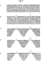
- the form of said rectangular recess is defined by a length L4, a width L1 and a breadth L2 of the remaining first conductive layer (see Figure 1 ).
- the biprism of the invention allows to produce inner electrodes with a width of less than 500 nm and even up to 50 nm.
- the inner electrode has a width of 50 nm and a length of between 1 and 5 mm, preferably between 2 and 3 mm and most preferably of 2.5 mm.
- the inner electrode of the biprism possess an aspect ratio (i.e. the ratio between width and height) of less than 1:1, preferably of less than 1:5 and more preferably of less than 1:10.
- the aspect ratio is between 1:2 and 1:20, preferably between 1:5 and 1:15 and more preferably between 1:8 and 1:12.
- the aspect ratio is a key factor for determining the interference wide and the contrast of the interference pattern.
- the supportive layer exhibits at least one cavity, preferably leaving the area forming the inner electrode uncovered from the support layer.
- the earth electrode can function as a counter electrode for two adjacent inner electrodes so that the following order of areas is given: EE-IE-EE-IE-EE-IE-EE...
- the inner electrodes and the earth electrodes are preferably lined in parallel.
- the individual biprisms can be of identical form and/or dimensions, whereby the inner electrodes and the adjacent earth cathodes are preferably all lined in parallel.
- the individual biprisms possess different shapes or forms thereby enabling different paths for the electron beam. This allows the possibility that the different paths which are available to the electron beam can be exposed to the electromagnetic field with different amplitude, frequency and/or phase shift.
- the electrostatic biprism of the invention can be produced by any microelectronic and nano-electronic fabrication method and typically by a method that is used for the production of semiconductor devices.
- semiconductor device fabrication the various processing steps fall into four general categories: deposition, removal, patterning, and modification of electrical properties.
- Deposition is any process that grows, coats, or otherwise transfers a material onto a base layer.
- Available technologies include physical vapour deposition (PVD), chemical vapour deposition (CVD), electrochemical deposition (ECD), molecular beam epitaxy (MBE) and more recently, atomic layer deposition (ALD) among others.
- Removal is any process that removes material from layered material; examples include etch processes (either wet or dry) and chemical-mechanical planarization (CMP).
- etch processes either wet or dry
- CMP chemical-mechanical planarization
- Patterning is the shaping or altering of deposited materials, and is generally referred to as optical lithography or electron beam lithography.
- the base layer is coated with a chemical called a photoresist; then, a machine called a stepper focuses, aligns, and moves a mask, exposing select portions of the base layer below to short wavelength light; the exposed regions are washed away by a developer solution. After etching or other processing, the remaining photoresist is removed by plasma ashing.
- Modification of electrical properties has historically entailed doping transistor sources and drains (originally by diffusion furnaces and later by ion implantation). These doping processes are followed by furnace annealing or, in advanced devices, by rapid thermal annealing (RTA); annealing serves to activate the implanted dopants. Modification of electrical properties now also extends to the reduction of a material's dielectric constant in low-k insulators via exposure to ultraviolet light in UV processing (UVP).
- UV processing ultraviolet light in UV processing
- the metal layer as optional element of the biprism of the invention can be made from any conductive metal.
- the metal layer on top of the conductive layer facilitates the electrical contact between the biprism and the external hardware.
- the conductive metal comprises not only pure metals but also doped metals and alloys.
- the metal layer consists of a metal selected from the group consisting of Al, AISi, Pt, Au and Ni.
- the first conductive layer of the biprism can be made from any conductive material, including but not limited to metals, superconductors, semiconductors, nonmetallic conductors such as graphite and conductive polymers.
- the first conductivity layer has a conductivity of 10 -6 S ⁇ m -1 or more, preferably of 10 -2 S ⁇ m -1 or more and more preferably of 10 S ⁇ m -1 or more.
- the conductive layer consists of a metal or a semiconductor, whereby silicon (Si), an aluminium alloy or platinum (Pt) are more preferred.
- the aluminium alloy preferably consists of a material selected from the group consisting of AlCuMg, AlCuSiMn, AlMgSi, AlZnMg, AlZnMgCu, AISi, AlSiMg, AlSiCu, AIMg, AlMgSi, AlCuTi, AlCuTiMg, whereby AISi is of further preference. More preferably, a hypereutectic AISi alloy is used. For the AISi alloys it is known that increasing the Si content results in an increase of the strength of hypoeutectic alloys and a decrease of the strength of hypereutectic alloys.
- the second non-conductive layer of the biprism of the invention can be made from any non-conductive, i.e., insulator material.
- An insulator material is a material whose internal electric charges do not flow freely, and therefore make it very hard to conduct an electric current under the influence of an electric field.
- the non-conductive material is a metal oxide or metal nitride.
- said second non-conductive layer consists of a material selected from the group consisting of SiO 2 , Si 3 N 4 , and HfO 2 , whereby SiO 2 is the most preferred material.
- the support layer can be made of any material that is suitable for nanofabrication. Preferably it consists of a material selected from the group consisting of mono- or polycrystalline silicon, GaAs, GaN, Al 2 O 3 , Pt and Al.
- the invention provides a method of producing an electrostatic biprism comprising the following steps:
- a silicon-on-sapphire (SOS) substrate is used in step a.
- SiO 2 -based SOI wafers can be produced by several methods:
- the method of producing the electrostatic biprism according to claim 10 comprises the following steps:
- the method of producing the electrostatic biprism according to claim 10 comprises the following steps:
- the substrate as provided in step a) is preferably mono crystalline to benefit of slopes in the back side cavity, whereas a poly-crystalline substrate is more cost-efficient.
- the electrostatic biprism can be used for any application which requires a beam splitter or an electrostatic deflection of charged particles. These charged particles could be molecules, atoms or even elementary particles.
- the electrostatic biprism is used as an electronic biprism within an electron beam device, which typically comprises an electron gun (consisting of a cathode, grid, and anode) which is used to generate and accelerate the primary beam, an electromagnetic optical focusing and/or deflection system and a target for the electron beam.
- an electron beam device typically comprises an electron gun (consisting of a cathode, grid, and anode) which is used to generate and accelerate the primary beam, an electromagnetic optical focusing and/or deflection system and a target for the electron beam.
- the electrostatic biprism can be used for every application for which a deflection or scattering of charged particles is required.
- the respective electron beam device is used for electron holography, filtering energy, transmission electron microscopy, generation of vortex electron beams, aberration corrections or phase plate.
- the electron biprism of the invention can be used for a scanning transmission electron microscope (STEM) or a transmission electron microscope (TEM).
- STEM scanning transmission electron microscope
- TEM transmission electron microscope
- the invention provides an electron beam device comprising an electron biprism according to the invention.
- the invention provides a microscope or interferometer comprising an electron biprism according to the invention.
- Electrostatic biprism in the context of the present invention is a device that allows a scattering or deflection of a beam of charged particles such as ions of molecules or atoms or elementary particles to generate two different beams of particles.
- the electrostatic biprism is denominated as an electron biprism.
- the inner electrode is the central electrode of an electrostatic biprism that in interaction with the two adjacent earth/ground electrodes builds an electromagnetic field for deflection or scattering of the charged particles.
- the freestanding electrode is the area of the conductive layer which has no underlying non-conductive layer and also no underlying support layer.
- the freestanding electrode is only attached by its two ends to the peripheral conductive layer, whereas alongside the inner electrode (optionally coated with a metal layer) it stands free from any material, especially from the second non-conductive layer. It has to be pronounced that the freestanding electrode still can be coated by the metal layer.
- the freestanding electrode mimics the filament of the prior art electron biprism.
- a "conductive layer” which is synonymous to an electronically conductive layer, encompasses any conductive material, including but not limited to metals, superconductors, semiconductors, nonmetallic conductors such as graphite and conductive polymers.
- a conductive layer it has a conductivity ⁇ which is 10 -6 S ⁇ m -1 or more.
- the "non-conductive layer” is a layer with electrically non-conductive or insulating properties. Hence it represents a material whose internal electric charges do not flow freely, and therefore make it very hard to conduct an electric current under the influence of an electric field. As such it has a resistance p of at least 10 4 ⁇ ⁇ m.
- a silicon-on-insulator (SOI) substrate is provided, with a silicon bottom layer, a thin SiO 2 layer (so called SiO 2 box) and a top silicon layer, whereby the thickness of the top silicon layer corresponds to the targeted height of the biprism plus the thickness of the layer that is lost because of oxidative fabrication steps.
- the thickness of said layer can be increased by an additional epitaxy step or conversely decreased in thickness by an additional oxidation step with subsequent oxide etching process.
- alignment patterns are etched into the surface of the top Si layer to ensure a correct front to back side alignment.
- the top Si layer is etched down to the buried SiO 2 layer to create the biprismatic structures and oxidised thereafter.
- back side cavities are created by chemical Si etching resulting in slopes that depend upon the choice of crystallographic orientation of the Si substrate. Slope for ⁇ 100> orientation is equal to 54°7. If back side cavity is etched using DRIE the resulting slope is very close to 90°.
- a thin metallic layer can be deposited on the surface of the Si top layer to facilitate the electrical contact between the biprism and the external hardware.
- the starting material would be a Si substrate layer.
- the non-conductive layer is generated on top of the Si substrate layer.
- deposition of a polycrystalline silicon layer on top of the non-conductive SiO 2 layer is performed by epitaxy or by low pressure chemical vapour deposition (LPCVD) to generate the first conductive layer.
- LPCVD low pressure chemical vapour deposition
- the resulting SOI substrate can be further processed as described in Example 1. Although the final device exhibits reduced mechanical stability, this process benefits from lower production costs.
Landscapes
- Chemical & Material Sciences (AREA)
- Analytical Chemistry (AREA)
- Crystals, And After-Treatments Of Crystals (AREA)
- Micromachines (AREA)
Claims (15)
- Elektrostatisches Doppelprisma, welches ein Streuen oder Ablenken eines Strahls geladener Partikel ermöglicht, um zwei verschiedene Partikelstrahlen zu erzeugen, mit einer ersten, leitfähigen Schicht, vorzugsweise einer mono- oder polykristallinen Schicht, die auf einer zweiten, nicht-leitfähigen Schicht angeordnet ist, welche auf einer Trägerschicht angeordnet ist, wobei mindestens ein Bereich der ersten, leitfähigen Schicht, welcher eine innere Elektrode als eine Mittelelektrode des elektrostatischen Doppelprismas bildet, von zwei benachbarten Bereichen der ersten, leitfähigen Schicht elektrisch isoliert ist, wobei die Trägerschicht einen Hohlraum unter der inneren Elektrode aufweist, die als eine freistehende Elektrode ohne darunter befindliche nicht-leitfähige Schicht und ohne darunter befindliche Trägerschicht und mit Spalten zwischen der inneren Elektrode und den beiden benachbarten Bereichen der ersten, leitfähigen Schicht ausgebildet ist.
- Elektrostatisches Doppelprisma nach Anspruch 1, bei welchem die Dicke der ersten, leitfähigen Schicht, welche die Höhe der inneren Elektrode des elektrostatischen Doppelprismas definiert, zwischen 10 nm und 1 mm, vorzugsweise zwischen 0,1 µm und 10 µm und stärker bevorzugt zwischen 0.5 und 2 µm beträgt,
und/oder
die Dicke der zweiten, nicht-leitfähigen Schicht zwischen 1 nm und 100 µm, vorzugsweise zwischen 25 nm und 500 nm und stärker bevorzugt zwischen 50 und 200 nm beträgt. - Elektrostatisches Doppelprisma nach einem der vorhergehenden Ansprüche, bei welchem die Trägerschicht eine Dicke zwischen 1 nm und 10 nm, vorzugsweise 100 nm und 5 mm und stärker bevorzugt zwischen 500 µm und 1 mm aufweist.
- Elektrostatisches Doppelprisma nach einem der vorhergehenden Ansprüche, bei welchem der Bereich der ersten, leitfähigen Schicht eine Form aufweist, die aus der Gruppe bestehend aus einer Spirale, einem Kreis, konzentrischen Kreisen und einem Rechteck gewählt ist.
- Elektrostatisches Doppelprisma nach einem der vorhergehenden Ansprüche, bei welchem der Spalt zwischen dem Bereich, welcher die innere Elektrode bildet, und den beiden benachbarten Elektroden durch eine Ausnehmung in der inneren Elektrode und/oder den benachbarten Bereichen erweitert ist,
wobei die Ausnehmung vorzugsweise rechteckig, dreieckig oder kreisförmig mit einer Seitenlänge L4 innerhalb der ersten, leitfähigen Schicht, einer Seitenweite L1 innerhalb der ersten, leitfähigen Schicht und einer Seitenbreite L2 der verbleibenden ersten, leitfähigen Schicht der freistehenden Elektrode aufweist. - Elektrostatisches Doppelprisma nach Anspruch 5, bei welchem ein Seitenverhältnis zwischen der Breite L2 und einer Höhe L3 der freistehenden inneren Elektrode kleiner als 1:1, vorzugsweise kleiner als 1:5, stärker bevorzugt kleiner als 1:10 ist.
oder
das elektrostatische Doppelprisma eines oder mehrere der folgenden Merkmale aufweist:(a) die Länge L4 liegt in einem Bereich zwischen 1 nm und 10 mm, vorzugsweise zwischen 1 µm und 1 mm und meist bevorzugt zwischen 1 µm und 100 µm;(b) die Weite L1 liegt in einem Bereich zwischen 1 nm und 10 µm, vorzugsweise zwischen 10 nm und 1 µm und meist bevorzugt zwischen 50 nm und 500 nm;(c) die Breite L2 der verbleibenden ersten, leitfähigen Schicht liegt in einem Bereich zwischen 1 nm und 100 µm, vorzugsweise zwischen 10 nm und 10 µm und meist bevorzugt zwischen 50 nm und 500 nm. - Elektrostatisches Doppelprisma nach einem der vorhergehenden Ansprüche, bei welchem die Substratschicht mindestens einen Hohlraum aufweist.
- Elektrostatisches Doppelprisma nach einem der vorhergehenden Ansprüche, bei welchem das elektrostatische Doppelprisma 2 bis 1000 Bereiche einer inneren Elektrode aufweist, die von zwei benachbarten Bereichen der ersten, leitfähigen Schicht elektrisch isoliert sind, vorzugsweise 2 bis 100 Bereiche, stärker bevorzugt 2 bis 10 Bereiche und meist bevorzugt 2 bis 5 Bereiche.
- Elektrostatisches Doppelprisma nach einem der vorhergehenden Ansprüche, bei welchem das elektrostatische Doppelprisma eines oder mehrere der folgenden Merkmale aufweist:(a) eine Metallschicht, die vorzugsweise aus einem Metall besteht, das aus der Gruppe bestehend aus Al, AISi, Pt, Au und Ni gewählt ist, ist auf der ersten, leitfähigen Schicht aufgebracht;(b) die erste, leitfähige Schicht besteht aus einem Material, das aus der Gruppe bestehend aus Si, AISi und Pt gewählt ist;(c) die zweite, nicht-leitfähige Schicht besteht aus einem Material, das aus der Gruppe bestehend aus SiO2, Si3N4 und HfO2 gewählt ist;(d) die Trägerschicht besteht aus einem Material, das aus der Gruppe bestehend aus mono- oder polykristallinem Silizium, GaAs, GaN, Al2O3, Pt und AI gewählt ist.
- Verfahren zur Herstellung eines elektrostatischen Doppelprismas nach Anspruch 1, mit den folgenden Schritten:(a) Vorsehen einer Schicht aus einem leitfähigen Material, welches auf einer auf einer Trägerschicht befindlichen Schicht aus einem nicht leitfähigen Material aufgebracht wird;(b) Durchführen eines Photo-/Elektronenstrahllithografievorgangs, optional in Kombination mit Ätz- und/oder Oxidationsschritten, um mindestens einen Bereich der ersten, leitfähigen Schicht, der eine innere Elektrode bildet, als eine Mittelelektrode des elektrostatischen Doppelprismas vorzusehen, die von zwei benachbarten Bereichen der ersten, leitfähigen Schicht elektrisch isoliert ist, wobei die Trägerschicht einen Hohlraum unter der inneren Elektrode aufweist, die als eine freistehende Elektrode ohne darunter befindliche nicht-leitfähige Schicht und ohne darunter befindliche Trägerschicht und mit Spalten zwischen der inneren Elektrode und den beiden benachbarten Bereichen der ersten, leitfähigen Schicht ausgebildet ist.
- Verfahren zur Herstellung eines elektrostatischen Doppelprismas nach Anspruch 10, mit den folgenden Schritten:(a) Vorsehen eines Silicon-On-Insulator-Subsrats (SOI), wobei das Silizium vorzugsweise aus monokristallinem Silizium und der Isolator vorzugsweise aus SiO2 besteht;(b) Ätzen von Ausrichtungsmarken in die Oberseite der aus Silizium bestehenden oberen Schicht;(c) Ätzen des den Bereich der inneren Elektrode umgebenden Ausnehmungsbereichs in die aus Silizium bestehende obere Schicht bis hinunter zur vergrabenen Isolatorschicht, welche vorzugsweise eine SiO2-Schicht ist;(d) Oxidieren des Elements, um eine SiO2-Schicht auf der aus Silizium bestehenden oberen Schicht zu bilden;(e) Ätzen mindestens eines Rückseitenhohlraums in eine Substratschicht durch chemisches Si-Ätzen oder Deep Reactive Ion Etching (DRIE);(f) Durchführen von isotropem Oxidätzen mittels nassem oder dampfförmigem HF zum Entfernen von erreichbaren Oxidschichten, um den Bereich der inneren Elektrode und die vergrabene Isolatorschicht zwischen diesem Bereich und dem Rückseitenhohlraum freizulegen;(g) optionales Aufbringen einer Metallschicht auf der Oberfläche der aus Silizium bestehenden oberen Schicht.
- Verfahren zur Herstellung eines elektrostatischen Doppelprismas nach Anspruch 10, mit den folgenden Schritten:(a) Vorsehen einer mono- oder polykristalline Siliziumsubstratschicht;(b) Oxidieren der Oberseite der Siliziumsubstratschicht zur Bildung einer SiO2-Schicht als die zweite, nicht leitfähige Schicht;(c) Aufbringen einer polykristallinen Siliziumschicht auf der nicht leitfähigen SiO2-Schicht durch Epitaxie oder durch chemische Niederdruck-Gasphasenabscheidung (LPCVD), um die erste, leitfähige Schicht zu bilden;(d) Ätzen von Ausrichtungsmarken in die Oberseite der aus Silizium bestehenden oberen Schicht;(e) Ätzen des den Bereich der inneren Elektrode umgebenden Ausnehmungsbereichs in die aus Silizium bestehende obere Schicht bis hinunter zur vergrabenen SiO2-Isolatorschicht;(f) Oxidieren des Elements, um eine SiO2-Schicht auf der aus Silizium bestehenden oberen Schicht zu bilden;(g) Ätzen mindestens eines Rückseitenhohlraums in eine Substratschicht durch chemisches Si-Ätzen oder Deep Reactive Ion Etching (DRIE);(h) Durchführen von isotropem Oxidätzen mittels nassem oder dampfförmigem HF zum Entfernen von erreichbaren Oxidschichten, um den Bereich der inneren Elektrode und die vergrabene Isolatorschicht zwischen diesem Bereich und dem Rückseitenhohlraum freizulegen;(i) optionales Aufbringen einer Metallschicht auf der Oberfläche der aus Silizium bestehenden oberen Schicht.
- Verwendung des elektrostatischen Doppelprismas nach Anspruch 1 als eine Elektronenstrahlvorrichtung für die Elektronenholografie, das Filtern von Energie, die Transmissionselektronenmikroskopie, das Erzeugen von Vortexelektronenstrahlen, Aberrationskorrekturen oder als Phasenplatte.
- Elektronenstrahlvorrichtung mit einem elektrostatischen Doppelprisma nach Anspruch 1.
- Mikroskop oder Interferometer mit einem elektrostatischen Doppelprisma nach Anspruch 1 oder einer Elektronenstrahlvorrichtung nach Anspruch 14.
Applications Claiming Priority (1)
| Application Number | Priority Date | Filing Date | Title |
|---|---|---|---|
| PCT/EP2014/077393 WO2016091314A1 (en) | 2014-12-11 | 2014-12-11 | Electrostatic biprism |
Publications (2)
| Publication Number | Publication Date |
|---|---|
| EP3231001A1 EP3231001A1 (de) | 2017-10-18 |
| EP3231001B1 true EP3231001B1 (de) | 2020-02-05 |
Family
ID=52146461
Family Applications (1)
| Application Number | Title | Priority Date | Filing Date |
|---|---|---|---|
| EP14818927.7A Active EP3231001B1 (de) | 2014-12-11 | 2014-12-11 | Elektrostatisches doppelprisma |
Country Status (2)
| Country | Link |
|---|---|
| EP (1) | EP3231001B1 (de) |
| WO (1) | WO2016091314A1 (de) |
Family Cites Families (3)
| Publication number | Priority date | Publication date | Assignee | Title |
|---|---|---|---|---|
| DE10206703A1 (de) * | 2002-02-18 | 2003-08-28 | Max Planck Gesellschaft | Phasenplatte für die Elektronenmikroskopie und elektronenmikroskopische Bildgebung |
| JP5335508B2 (ja) * | 2009-03-25 | 2013-11-06 | 一般財団法人ファインセラミックスセンター | 緊張化した空中配線の形成方法、荷電粒子線プリズムとその製造方法、荷電粒子線の干渉縞を用いた観察方法、電子顕微鏡および電子顕微鏡における干渉縞の形成方法 |
| KR101455743B1 (ko) * | 2013-07-03 | 2014-11-03 | 서울대학교산학협력단 | 저항 변화를 기반으로 한 나노 스케일의 전자기계적 구조의 스위치 소자 |
-
2014
- 2014-12-11 EP EP14818927.7A patent/EP3231001B1/de active Active
- 2014-12-11 WO PCT/EP2014/077393 patent/WO2016091314A1/en not_active Ceased
Non-Patent Citations (1)
| Title |
|---|
| None * |
Also Published As
| Publication number | Publication date |
|---|---|
| EP3231001A1 (de) | 2017-10-18 |
| WO2016091314A1 (en) | 2016-06-16 |
Similar Documents
| Publication | Publication Date | Title |
|---|---|---|
| US10734525B2 (en) | Gate-all-around transistor with spacer support and methods of forming same | |
| EP0511360B1 (de) | Elektronenquelle und herstellungsverfahren | |
| US10170581B2 (en) | FinFET with reduced parasitic capacitance | |
| KR101857915B1 (ko) | 상호접속 구조물 및 상호접속 구조물의 형성 방법 | |
| US20040195612A1 (en) | Method of creating deep trench capacitor using a p+ metal electrode | |
| US20200144498A1 (en) | Bottom electrode for semiconductor memory device | |
| US10461196B2 (en) | Control of length in gate region during processing of VFET structures | |
| US20200119203A1 (en) | Gate All-Around Device | |
| US12402542B2 (en) | Josephson transistor | |
| US20200295256A1 (en) | Replacement bottom electrode structure process to form misalignment tolerate mram with high yield | |
| US10056329B1 (en) | Programmable buried antifuse | |
| KR20240158286A (ko) | 후면 전원 공급을 위한 하이브리드 유전체 방식의 스킵-레벨 tsv | |
| US20120168711A1 (en) | Narrow-Waist Nanowire Transistor with Wide Aspect Ratio Ends | |
| US20240072041A1 (en) | Integration of Nanosheets with Bottom Dielectric Isolation and Ideal Diode | |
| JP2005508571A (ja) | カーボン含有アンチヒューズ材料を使用した金属対金属アンチヒューズ | |
| WO2022001592A1 (zh) | 半导体结构及其制作方法 | |
| TW200931621A (en) | Semiconductor structure comprising an electrically conductive feature and method of forming a semiconductor structure | |
| US10658494B2 (en) | Transistors and methods of forming transistors using vertical nanowires | |
| US10109722B2 (en) | Etch-resistant spacer formation on gate structure | |
| Killge et al. | Copper-based TSV: Interposer | |
| EP3231001A1 (de) | Elektrostatisches doppelprisma | |
| CN204905205U (zh) | 集成真空微电子结构 | |
| TW202131396A (zh) | 半導體裝置及其形成方法 | |
| TW202109624A (zh) | 積體電路的製作方法 | |
| TW514995B (en) | Semiconductor device and method for fabricating a semiconductor device |
Legal Events
| Date | Code | Title | Description |
|---|---|---|---|
| STAA | Information on the status of an ep patent application or granted ep patent |
Free format text: STATUS: THE INTERNATIONAL PUBLICATION HAS BEEN MADE |
|
| PUAI | Public reference made under article 153(3) epc to a published international application that has entered the european phase |
Free format text: ORIGINAL CODE: 0009012 |
|
| STAA | Information on the status of an ep patent application or granted ep patent |
Free format text: STATUS: REQUEST FOR EXAMINATION WAS MADE |
|
| 17P | Request for examination filed |
Effective date: 20170711 |
|
| AK | Designated contracting states |
Kind code of ref document: A1 Designated state(s): AL AT BE BG CH CY CZ DE DK EE ES FI FR GB GR HR HU IE IS IT LI LT LU LV MC MK MT NL NO PL PT RO RS SE SI SK SM TR |
|
| AX | Request for extension of the european patent |
Extension state: BA ME |
|
| RIN1 | Information on inventor provided before grant (corrected) |
Inventor name: DUNIN-BORKOWSKI, RAFAL EDWARD Inventor name: COOPER, DAVID Inventor name: DUCHAMP, MARTIAL Inventor name: GIRARD, OLIVIER |
|
| DAX | Request for extension of the european patent (deleted) | ||
| GRAP | Despatch of communication of intention to grant a patent |
Free format text: ORIGINAL CODE: EPIDOSNIGR1 |
|
| STAA | Information on the status of an ep patent application or granted ep patent |
Free format text: STATUS: GRANT OF PATENT IS INTENDED |
|
| INTG | Intention to grant announced |
Effective date: 20180730 |
|
| GRAJ | Information related to disapproval of communication of intention to grant by the applicant or resumption of examination proceedings by the epo deleted |
Free format text: ORIGINAL CODE: EPIDOSDIGR1 |
|
| STAA | Information on the status of an ep patent application or granted ep patent |
Free format text: STATUS: REQUEST FOR EXAMINATION WAS MADE |
|
| INTC | Intention to grant announced (deleted) | ||
| GRAP | Despatch of communication of intention to grant a patent |
Free format text: ORIGINAL CODE: EPIDOSNIGR1 |
|
| STAA | Information on the status of an ep patent application or granted ep patent |
Free format text: STATUS: GRANT OF PATENT IS INTENDED |
|
| INTG | Intention to grant announced |
Effective date: 20190104 |
|
| GRAJ | Information related to disapproval of communication of intention to grant by the applicant or resumption of examination proceedings by the epo deleted |
Free format text: ORIGINAL CODE: EPIDOSDIGR1 |
|
| STAA | Information on the status of an ep patent application or granted ep patent |
Free format text: STATUS: REQUEST FOR EXAMINATION WAS MADE |
|
| INTC | Intention to grant announced (deleted) | ||
| GRAP | Despatch of communication of intention to grant a patent |
Free format text: ORIGINAL CODE: EPIDOSNIGR1 |
|
| STAA | Information on the status of an ep patent application or granted ep patent |
Free format text: STATUS: GRANT OF PATENT IS INTENDED |
|
| INTG | Intention to grant announced |
Effective date: 20190627 |
|
| GRAS | Grant fee paid |
Free format text: ORIGINAL CODE: EPIDOSNIGR3 |
|
| GRAA | (expected) grant |
Free format text: ORIGINAL CODE: 0009210 |
|
| STAA | Information on the status of an ep patent application or granted ep patent |
Free format text: STATUS: THE PATENT HAS BEEN GRANTED |
|
| AK | Designated contracting states |
Kind code of ref document: B1 Designated state(s): AL AT BE BG CH CY CZ DE DK EE ES FI FR GB GR HR HU IE IS IT LI LT LU LV MC MK MT NL NO PL PT RO RS SE SI SK SM TR |
|
| REG | Reference to a national code |
Ref country code: GB Ref legal event code: FG4D |
|
| REG | Reference to a national code |
Ref country code: AT Ref legal event code: REF Ref document number: 1230464 Country of ref document: AT Kind code of ref document: T Effective date: 20200215 |
|
| REG | Reference to a national code |
Ref country code: DE Ref legal event code: R096 Ref document number: 602014060654 Country of ref document: DE |
|
| REG | Reference to a national code |
Ref country code: IE Ref legal event code: FG4D |
|
| REG | Reference to a national code |
Ref country code: CH Ref legal event code: EP |
|
| REG | Reference to a national code |
Ref country code: NL Ref legal event code: FP |
|
| PG25 | Lapsed in a contracting state [announced via postgrant information from national office to epo] |
Ref country code: RS Free format text: LAPSE BECAUSE OF FAILURE TO SUBMIT A TRANSLATION OF THE DESCRIPTION OR TO PAY THE FEE WITHIN THE PRESCRIBED TIME-LIMIT Effective date: 20200205 Ref country code: NO Free format text: LAPSE BECAUSE OF FAILURE TO SUBMIT A TRANSLATION OF THE DESCRIPTION OR TO PAY THE FEE WITHIN THE PRESCRIBED TIME-LIMIT Effective date: 20200505 Ref country code: PT Free format text: LAPSE BECAUSE OF FAILURE TO SUBMIT A TRANSLATION OF THE DESCRIPTION OR TO PAY THE FEE WITHIN THE PRESCRIBED TIME-LIMIT Effective date: 20200628 Ref country code: FI Free format text: LAPSE BECAUSE OF FAILURE TO SUBMIT A TRANSLATION OF THE DESCRIPTION OR TO PAY THE FEE WITHIN THE PRESCRIBED TIME-LIMIT Effective date: 20200205 |
|
| REG | Reference to a national code |
Ref country code: LT Ref legal event code: MG4D |
|
| PG25 | Lapsed in a contracting state [announced via postgrant information from national office to epo] |
Ref country code: HR Free format text: LAPSE BECAUSE OF FAILURE TO SUBMIT A TRANSLATION OF THE DESCRIPTION OR TO PAY THE FEE WITHIN THE PRESCRIBED TIME-LIMIT Effective date: 20200205 Ref country code: IS Free format text: LAPSE BECAUSE OF FAILURE TO SUBMIT A TRANSLATION OF THE DESCRIPTION OR TO PAY THE FEE WITHIN THE PRESCRIBED TIME-LIMIT Effective date: 20200605 Ref country code: SE Free format text: LAPSE BECAUSE OF FAILURE TO SUBMIT A TRANSLATION OF THE DESCRIPTION OR TO PAY THE FEE WITHIN THE PRESCRIBED TIME-LIMIT Effective date: 20200205 Ref country code: LV Free format text: LAPSE BECAUSE OF FAILURE TO SUBMIT A TRANSLATION OF THE DESCRIPTION OR TO PAY THE FEE WITHIN THE PRESCRIBED TIME-LIMIT Effective date: 20200205 Ref country code: GR Free format text: LAPSE BECAUSE OF FAILURE TO SUBMIT A TRANSLATION OF THE DESCRIPTION OR TO PAY THE FEE WITHIN THE PRESCRIBED TIME-LIMIT Effective date: 20200506 Ref country code: BG Free format text: LAPSE BECAUSE OF FAILURE TO SUBMIT A TRANSLATION OF THE DESCRIPTION OR TO PAY THE FEE WITHIN THE PRESCRIBED TIME-LIMIT Effective date: 20200505 |
|
| PG25 | Lapsed in a contracting state [announced via postgrant information from national office to epo] |
Ref country code: SM Free format text: LAPSE BECAUSE OF FAILURE TO SUBMIT A TRANSLATION OF THE DESCRIPTION OR TO PAY THE FEE WITHIN THE PRESCRIBED TIME-LIMIT Effective date: 20200205 Ref country code: SK Free format text: LAPSE BECAUSE OF FAILURE TO SUBMIT A TRANSLATION OF THE DESCRIPTION OR TO PAY THE FEE WITHIN THE PRESCRIBED TIME-LIMIT Effective date: 20200205 Ref country code: RO Free format text: LAPSE BECAUSE OF FAILURE TO SUBMIT A TRANSLATION OF THE DESCRIPTION OR TO PAY THE FEE WITHIN THE PRESCRIBED TIME-LIMIT Effective date: 20200205 Ref country code: CZ Free format text: LAPSE BECAUSE OF FAILURE TO SUBMIT A TRANSLATION OF THE DESCRIPTION OR TO PAY THE FEE WITHIN THE PRESCRIBED TIME-LIMIT Effective date: 20200205 Ref country code: LT Free format text: LAPSE BECAUSE OF FAILURE TO SUBMIT A TRANSLATION OF THE DESCRIPTION OR TO PAY THE FEE WITHIN THE PRESCRIBED TIME-LIMIT Effective date: 20200205 Ref country code: ES Free format text: LAPSE BECAUSE OF FAILURE TO SUBMIT A TRANSLATION OF THE DESCRIPTION OR TO PAY THE FEE WITHIN THE PRESCRIBED TIME-LIMIT Effective date: 20200205 Ref country code: EE Free format text: LAPSE BECAUSE OF FAILURE TO SUBMIT A TRANSLATION OF THE DESCRIPTION OR TO PAY THE FEE WITHIN THE PRESCRIBED TIME-LIMIT Effective date: 20200205 Ref country code: DK Free format text: LAPSE BECAUSE OF FAILURE TO SUBMIT A TRANSLATION OF THE DESCRIPTION OR TO PAY THE FEE WITHIN THE PRESCRIBED TIME-LIMIT Effective date: 20200205 |
|
| REG | Reference to a national code |
Ref country code: DE Ref legal event code: R097 Ref document number: 602014060654 Country of ref document: DE |
|
| REG | Reference to a national code |
Ref country code: AT Ref legal event code: MK05 Ref document number: 1230464 Country of ref document: AT Kind code of ref document: T Effective date: 20200205 |
|
| PLBE | No opposition filed within time limit |
Free format text: ORIGINAL CODE: 0009261 |
|
| STAA | Information on the status of an ep patent application or granted ep patent |
Free format text: STATUS: NO OPPOSITION FILED WITHIN TIME LIMIT |
|
| 26N | No opposition filed |
Effective date: 20201106 |
|
| PG25 | Lapsed in a contracting state [announced via postgrant information from national office to epo] |
Ref country code: AT Free format text: LAPSE BECAUSE OF FAILURE TO SUBMIT A TRANSLATION OF THE DESCRIPTION OR TO PAY THE FEE WITHIN THE PRESCRIBED TIME-LIMIT Effective date: 20200205 Ref country code: IT Free format text: LAPSE BECAUSE OF FAILURE TO SUBMIT A TRANSLATION OF THE DESCRIPTION OR TO PAY THE FEE WITHIN THE PRESCRIBED TIME-LIMIT Effective date: 20200205 |
|
| PG25 | Lapsed in a contracting state [announced via postgrant information from national office to epo] |
Ref country code: SI Free format text: LAPSE BECAUSE OF FAILURE TO SUBMIT A TRANSLATION OF THE DESCRIPTION OR TO PAY THE FEE WITHIN THE PRESCRIBED TIME-LIMIT Effective date: 20200205 Ref country code: PL Free format text: LAPSE BECAUSE OF FAILURE TO SUBMIT A TRANSLATION OF THE DESCRIPTION OR TO PAY THE FEE WITHIN THE PRESCRIBED TIME-LIMIT Effective date: 20200205 |
|
| PG25 | Lapsed in a contracting state [announced via postgrant information from national office to epo] |
Ref country code: MC Free format text: LAPSE BECAUSE OF FAILURE TO SUBMIT A TRANSLATION OF THE DESCRIPTION OR TO PAY THE FEE WITHIN THE PRESCRIBED TIME-LIMIT Effective date: 20200205 |
|
| PG25 | Lapsed in a contracting state [announced via postgrant information from national office to epo] |
Ref country code: IE Free format text: LAPSE BECAUSE OF NON-PAYMENT OF DUE FEES Effective date: 20201211 Ref country code: LU Free format text: LAPSE BECAUSE OF NON-PAYMENT OF DUE FEES Effective date: 20201211 |
|
| PG25 | Lapsed in a contracting state [announced via postgrant information from national office to epo] |
Ref country code: TR Free format text: LAPSE BECAUSE OF FAILURE TO SUBMIT A TRANSLATION OF THE DESCRIPTION OR TO PAY THE FEE WITHIN THE PRESCRIBED TIME-LIMIT Effective date: 20200205 Ref country code: MT Free format text: LAPSE BECAUSE OF FAILURE TO SUBMIT A TRANSLATION OF THE DESCRIPTION OR TO PAY THE FEE WITHIN THE PRESCRIBED TIME-LIMIT Effective date: 20200205 Ref country code: CY Free format text: LAPSE BECAUSE OF FAILURE TO SUBMIT A TRANSLATION OF THE DESCRIPTION OR TO PAY THE FEE WITHIN THE PRESCRIBED TIME-LIMIT Effective date: 20200205 |
|
| PG25 | Lapsed in a contracting state [announced via postgrant information from national office to epo] |
Ref country code: MK Free format text: LAPSE BECAUSE OF FAILURE TO SUBMIT A TRANSLATION OF THE DESCRIPTION OR TO PAY THE FEE WITHIN THE PRESCRIBED TIME-LIMIT Effective date: 20200205 Ref country code: AL Free format text: LAPSE BECAUSE OF FAILURE TO SUBMIT A TRANSLATION OF THE DESCRIPTION OR TO PAY THE FEE WITHIN THE PRESCRIBED TIME-LIMIT Effective date: 20200205 |
|
| P01 | Opt-out of the competence of the unified patent court (upc) registered |
Effective date: 20230523 |
|
| PGFP | Annual fee paid to national office [announced via postgrant information from national office to epo] |
Ref country code: GB Payment date: 20231220 Year of fee payment: 10 |
|
| PGFP | Annual fee paid to national office [announced via postgrant information from national office to epo] |
Ref country code: NL Payment date: 20231219 Year of fee payment: 10 Ref country code: FR Payment date: 20231219 Year of fee payment: 10 |
|
| PGFP | Annual fee paid to national office [announced via postgrant information from national office to epo] |
Ref country code: BE Payment date: 20231218 Year of fee payment: 10 |
|
| PGFP | Annual fee paid to national office [announced via postgrant information from national office to epo] |
Ref country code: DE Payment date: 20231222 Year of fee payment: 10 Ref country code: CH Payment date: 20240110 Year of fee payment: 10 |
|
| REG | Reference to a national code |
Ref country code: DE Ref legal event code: R119 Ref document number: 602014060654 Country of ref document: DE |
|
| REG | Reference to a national code |
Ref country code: CH Ref legal event code: PL |
|
| REG | Reference to a national code |
Ref country code: NL Ref legal event code: MM Effective date: 20250101 |
|
| GBPC | Gb: european patent ceased through non-payment of renewal fee |
Effective date: 20241211 |
|
| PG25 | Lapsed in a contracting state [announced via postgrant information from national office to epo] |
Ref country code: NL Free format text: LAPSE BECAUSE OF NON-PAYMENT OF DUE FEES Effective date: 20250101 |
|
| REG | Reference to a national code |
Ref country code: BE Ref legal event code: MM Effective date: 20241231 |
|
| PG25 | Lapsed in a contracting state [announced via postgrant information from national office to epo] |
Ref country code: DE Free format text: LAPSE BECAUSE OF NON-PAYMENT OF DUE FEES Effective date: 20250701 |
|
| PG25 | Lapsed in a contracting state [announced via postgrant information from national office to epo] |
Ref country code: GB Free format text: LAPSE BECAUSE OF NON-PAYMENT OF DUE FEES Effective date: 20241211 Ref country code: BE Free format text: LAPSE BECAUSE OF NON-PAYMENT OF DUE FEES Effective date: 20241231 |
|
| PG25 | Lapsed in a contracting state [announced via postgrant information from national office to epo] |
Ref country code: FR Free format text: LAPSE BECAUSE OF NON-PAYMENT OF DUE FEES Effective date: 20241231 |
|
| PG25 | Lapsed in a contracting state [announced via postgrant information from national office to epo] |
Ref country code: CH Free format text: LAPSE BECAUSE OF NON-PAYMENT OF DUE FEES Effective date: 20241231 |