EP3229363B1 - Power converter - Google Patents
Power converter Download PDFInfo
- Publication number
- EP3229363B1 EP3229363B1 EP17159260.3A EP17159260A EP3229363B1 EP 3229363 B1 EP3229363 B1 EP 3229363B1 EP 17159260 A EP17159260 A EP 17159260A EP 3229363 B1 EP3229363 B1 EP 3229363B1
- Authority
- EP
- European Patent Office
- Prior art keywords
- power
- power converter
- converter according
- nodes
- electrode
- Prior art date
- Legal status (The legal status is an assumption and is not a legal conclusion. Google has not performed a legal analysis and makes no representation as to the accuracy of the status listed.)
- Active
Links
Images


Classifications
-
- H—ELECTRICITY
- H02—GENERATION; CONVERSION OR DISTRIBUTION OF ELECTRIC POWER
- H02M—APPARATUS FOR CONVERSION BETWEEN AC AND AC, BETWEEN AC AND DC, OR BETWEEN DC AND DC, AND FOR USE WITH MAINS OR SIMILAR POWER SUPPLY SYSTEMS; CONVERSION OF DC OR AC INPUT POWER INTO SURGE OUTPUT POWER; CONTROL OR REGULATION THEREOF
- H02M1/00—Details of apparatus for conversion
- H02M1/12—Arrangements for reducing harmonics from ac input or output
- H02M1/126—Arrangements for reducing harmonics from ac input or output using passive filters
-
- H—ELECTRICITY
- H02—GENERATION; CONVERSION OR DISTRIBUTION OF ELECTRIC POWER
- H02M—APPARATUS FOR CONVERSION BETWEEN AC AND AC, BETWEEN AC AND DC, OR BETWEEN DC AND DC, AND FOR USE WITH MAINS OR SIMILAR POWER SUPPLY SYSTEMS; CONVERSION OF DC OR AC INPUT POWER INTO SURGE OUTPUT POWER; CONTROL OR REGULATION THEREOF
- H02M1/00—Details of apparatus for conversion
- H02M1/12—Arrangements for reducing harmonics from ac input or output
-
- H—ELECTRICITY
- H02—GENERATION; CONVERSION OR DISTRIBUTION OF ELECTRIC POWER
- H02M—APPARATUS FOR CONVERSION BETWEEN AC AND AC, BETWEEN AC AND DC, OR BETWEEN DC AND DC, AND FOR USE WITH MAINS OR SIMILAR POWER SUPPLY SYSTEMS; CONVERSION OF DC OR AC INPUT POWER INTO SURGE OUTPUT POWER; CONTROL OR REGULATION THEREOF
- H02M3/00—Conversion of dc power input into dc power output
- H02M3/02—Conversion of dc power input into dc power output without intermediate conversion into ac
- H02M3/04—Conversion of dc power input into dc power output without intermediate conversion into ac by static converters
- H02M3/10—Conversion of dc power input into dc power output without intermediate conversion into ac by static converters using discharge tubes with control electrode or semiconductor devices with control electrode
- H02M3/145—Conversion of dc power input into dc power output without intermediate conversion into ac by static converters using discharge tubes with control electrode or semiconductor devices with control electrode using devices of a triode or transistor type requiring continuous application of a control signal
- H02M3/155—Conversion of dc power input into dc power output without intermediate conversion into ac by static converters using discharge tubes with control electrode or semiconductor devices with control electrode using devices of a triode or transistor type requiring continuous application of a control signal using semiconductor devices only
-
- H—ELECTRICITY
- H02—GENERATION; CONVERSION OR DISTRIBUTION OF ELECTRIC POWER
- H02M—APPARATUS FOR CONVERSION BETWEEN AC AND AC, BETWEEN AC AND DC, OR BETWEEN DC AND DC, AND FOR USE WITH MAINS OR SIMILAR POWER SUPPLY SYSTEMS; CONVERSION OF DC OR AC INPUT POWER INTO SURGE OUTPUT POWER; CONTROL OR REGULATION THEREOF
- H02M7/00—Conversion of ac power input into dc power output; Conversion of dc power input into ac power output
- H02M7/003—Constructional details, e.g. physical layout, assembly, wiring or busbar connections
-
- H—ELECTRICITY
- H02—GENERATION; CONVERSION OR DISTRIBUTION OF ELECTRIC POWER
- H02M—APPARATUS FOR CONVERSION BETWEEN AC AND AC, BETWEEN AC AND DC, OR BETWEEN DC AND DC, AND FOR USE WITH MAINS OR SIMILAR POWER SUPPLY SYSTEMS; CONVERSION OF DC OR AC INPUT POWER INTO SURGE OUTPUT POWER; CONTROL OR REGULATION THEREOF
- H02M7/00—Conversion of ac power input into dc power output; Conversion of dc power input into ac power output
- H02M7/42—Conversion of dc power input into ac power output without possibility of reversal
- H02M7/44—Conversion of dc power input into ac power output without possibility of reversal by static converters
- H02M7/48—Conversion of dc power input into ac power output without possibility of reversal by static converters using discharge tubes with control electrode or semiconductor devices with control electrode
- H02M7/53—Conversion of dc power input into ac power output without possibility of reversal by static converters using discharge tubes with control electrode or semiconductor devices with control electrode using devices of a triode or transistor type requiring continuous application of a control signal
- H02M7/537—Conversion of dc power input into ac power output without possibility of reversal by static converters using discharge tubes with control electrode or semiconductor devices with control electrode using devices of a triode or transistor type requiring continuous application of a control signal using semiconductor devices only, e.g. single switched pulse inverters
- H02M7/5387—Conversion of dc power input into ac power output without possibility of reversal by static converters using discharge tubes with control electrode or semiconductor devices with control electrode using devices of a triode or transistor type requiring continuous application of a control signal using semiconductor devices only, e.g. single switched pulse inverters in a bridge configuration
-
- H—ELECTRICITY
- H02—GENERATION; CONVERSION OR DISTRIBUTION OF ELECTRIC POWER
- H02M—APPARATUS FOR CONVERSION BETWEEN AC AND AC, BETWEEN AC AND DC, OR BETWEEN DC AND DC, AND FOR USE WITH MAINS OR SIMILAR POWER SUPPLY SYSTEMS; CONVERSION OF DC OR AC INPUT POWER INTO SURGE OUTPUT POWER; CONTROL OR REGULATION THEREOF
- H02M1/00—Details of apparatus for conversion
- H02M1/12—Arrangements for reducing harmonics from ac input or output
- H02M1/123—Suppression of common mode voltage or current
Definitions
- the present invention relates to a power converter.
- a power converter (system interconnection inverter) is used to convert DC power, generated in a photovoltaic power system or the like, into AC power and supply it to a power system.
- This power converter includes: a boosting converter configured to boost a DC voltage; and an inverter configured to convert the direct current into alternating current.
- common mode voltage neutral point potential
- a single-phase inverter has an H bridge configuration employing a switching element, and is subjected to 3-level PWM control, for example. Due to this control, common mode voltage is fluctuated. The fluctuation of the common mode voltage causes leakage current flowing to a ground (earth) and high-frequency noise. The high-frequency noise is reduced by inserting a common mode choke coil between a pair of output terminals of a DC power supply and a pair of input terminals of a boosting circuit (see Japanese Patent Laying-Open No. 2011-147238 ).
- a power converter according to the preamble of claim 1 is known from DE 10 2013 100246 A1 .
- a conventional common mode choke coil can reduce noise in a low frequency region such as a switching frequency.
- the noise reduction effect is low in a high frequency region such as a ringing frequency and a frequency of a harmonic wave thereof.
- the present invention aims to provide a power converter that provides a sufficient noise reduction effect in a high frequency region.
- a power converter according to a first aspect of the present invention comprises:
- the power converter further includes a plurality of capacitors each including a first electrode and a second electrode, the first electrode being connected to a corresponding one of the plurality of nodes, the second electrode being connected to the ground conductor.
- the plurality of inductors are each inserted between the corresponding one of the plurality of external terminals and the corresponding one of the plurality of nodes are inductively coupled with the other inductor inserted between the ground conductor and the earth terminal to construct a common mode choke coil having not less than three phases.
- the noise reduction effect can be increased.
- the plurality of external terminals are connected to a DC power supply, and the power conversion circuit is configured to receive DC power from the plurality of nodes, convert the DC power into AC power and output the AC power.
- the common mode noise leaking from the power converter to the DC power supply can be reduced.
- the plurality of external terminals are connected to a power system, and the power conversion circuit is configured to receive DC power, convert the DC power into AC power, and output the converted AC power from the plurality of nodes to the power system.
- the common mode noise leaking from the power converter to the power system can be reduced.
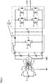
- Fig. 1 shows an equivalent circuit diagram of the power converter according to the first embodiment.
- the power converter according to the first embodiment includes external terminals T1, T2, an earth terminal TE, a common mode choke coil 18, and a power conversion circuit 10.
- Power conversion circuit 10 includes a boosting converter 20 and an inverter 30, and is configured to receive DC power, convert the DC power into AC power, and output the AC power.
- External terminals T1 and T2 are connected to positive electrode and negative electrode of a DC power supply 50 via a positive line 51 and a negative line 52.
- Earth terminal TE is connected (grounded) to the ground via an earth line 53, and is fixed to the same potential as that of the earth.
- DC power supply 50 a solar panel, a fuel cell, or the like is used, for example.
- External terminals T1 and T2 are connected to nodes N1 and N2 of power conversion circuit 10 via common mode choke coil 18.
- One electrode (first electrode) of a capacitor 11 is connected to node N1.
- One electrode (first electrode) of a capacitor 12 is connected to node N2.
- the other electrode (second electrode) of capacitor 11 is connected to the other electrode (second electrode) of capacitor 12.
- a point via which the second electrode of capacitor 11 and the second electrode of capacitor 12 are connected to each other will be referred to as an interconnection point P1.
- Interconnection point P1 is connected to a ground conductor of power conversion circuit 10.
- a potential of the ground conductor serves as a reference potential (ground potential) of the power conversion circuit.
- a metal housing or the like is used as the ground conductor.
- Capacitors, such as capacitors 11, 12, connected between a signal line (power supply line) and the ground conductor is commonly referred to as "Y capacitor". In the present specification, a capacitor connected between the signal line (power supply line) and the ground conductor is referred to as "Y capacitor".
- Common mode choke coil 18 includes three inductors 15, 16, 17.
- Inductor 15 is inserted between external terminal T1 and node N1.
- Inductor 16 is inserted between external terminal T2 and node N2.
- Inductor 17 is connected between interconnection point P1 and earth terminal TE.
- Common mode choke coil 18 is connected such that magnetic fluxes generated by common mode noise current flowing from power conversion circuit 10 to external terminals T1, T2 and earth terminal TE are intensified with one another.
- Boosting converter 20 includes a reactor 21, a free wheel diode 22, and a switching element 23. Diode 24 is connected to switching element 23 in parallel. An output of boosting converter 20 is sent to inverter 30. A smoothing capacitor 40 is connected to a DC line at the output side of boosting converter 20.
- Inverter 30 includes four switching elements 31, 32, 33, 34 connected to configure H bridge, for example.
- An interconnection point between switching elements 31 and 32 serves as a node N3 for outputting single-phase AC power
- an interconnection point between switching elements 33 and 34 serves as a node N4 for outputting single-phase AC power.
- switching elements 23, 31, 32, 33, 34 power semiconductor elements are used, for example.
- Each of the power semiconductor elements is generally in contact with a ground conductor such as a housing in order to dissipate heat generated by an operation thereof, and the ground conductor is used as a heat sink. Therefore, due to electromagnetic coupling between each of switching elements 23, 31, 32, 33, 34 and the ground conductor, noise generated in response to a switching operation is more likely to be propagated to the ground conductor.
- FIG. 2A and Fig. 2B shows a connection configuration among external terminals T1, T2, earth terminal TE, power conversion circuit 10, and DC power supply 50 in the power converter used in the experiment.
- Nodes N1, N2 of power conversion circuit 10 are directly connected to external terminals T1, T2, respectively.
- Interconnection point P1 between Y capacitors 11 and 12 is directly connected to earth terminal TE.
- External terminals T1 and T2 are connected to the positive electrode and negative electrode of DC power supply 50 via positive line 51 and negative line 52, respectively.
- Earth terminal TE is grounded by earth line 53.
- the level of noise generated from positive line 51, negative line 52, and earth line 53 was measured using a measuring instrument 55.
- noise level measured with two lines i.e., positive line 51 and negative line 52
- noise level measured with three lines i.e., positive line 51, negative line 52, and earth line 53
- the noise level measured by the method of Fig. 2B is lower than the noise level measured by the method of Fig. 2A ; however, in a high frequency region of not less than 1 MHz, there was found no large difference therebetween.
- Fig. 3B shows an equivalent circuit diagram of the power converter according to the comparative example.
- interconnection point P1 of Y capacitors 11, 12 is directly connected to earth terminal TE, not via common mode choke coil 18.
- An inductor not used among the three inductors of common mode choke coil 18 is in an open state.
- the other configurations are the same as those of the power converter according to the first embodiment.
- Fig. 3A shows a result of measurement of the noise levels of the power converters according to the first embodiment ( Fig. 1 ) and the comparative example ( Fig. 3B ).
- the horizontal axis represents the frequency based on "MHz" as a unit and the vertical axis represents the noise level based on "dB ⁇ V" as a unit.
- a thick solid line a1 in Fig. 3A represents the level of noise leaking from external terminal T2 of the power converter according to the first embodiment into negative line 52
- a thin solid line a2 represents the level of noise leaking from external terminal T2 of the power converter according to the comparative example into negative line 52.
- the noise levels at 1.2 MHz and 25 MHz are decreased as compared with the configuration of the comparative example. Particularly, the decrease of the noise level around the frequency of 25 MHz is remarkable.
- the decrease of the noise level is attained by inserting three-phase common mode choke coil 18 in positive line 51, negative line 52, and earth line 53.
- an impedance from nodes N1, N2 of power conversion circuit 10 to the ground point becomes high. Accordingly, leakage current flowing to earth line 53 can be reduced.
- a direct current flowing through inductor 15 inserted in positive line 51 is opposite in direction to a direct current flowing through inductor 16 inserted in negative line 52. Magnetic fluxes generated by these direct currents serve to cancel each other, whereby magnetic cores of inductors 15, 16 are unlikely to be saturated.
- Y capacitors 11, 12 are not necessarily provided. Y capacitors 11, 12 can be omitted.
- inductor 17 connects the ground conductor to earth terminal TE.
- Fig. 4 shows an equivalent circuit diagram of the power converter according to the second embodiment.
- three-phase common mode choke coil 18 is constituted of inductors 15, 16, 17 ( Fig. 1 ).
- inductors 15, 16, 17 are constituted of individual coils and are not inductively coupled with one another. Electromagnetic properties of three inductors 15, 16, 17 are the same.
- FIG. 5A and Fig. 5B electric properties of inductors 15, 16, 17 will be described.
- a two-terminal pair circuit shown in Fig. 5B was constructed using inductor 15, and a transmission property S21 was measured.
- Fig. 5A shows a result of measurement of transmission property S21.
- the horizontal axis represents the frequency based on "MHz" as a unit and the vertical axis represents transmission property S21 based on "dB" as a unit.
- S21 is smaller, insertion loss is larger.
- insertion loss exhibits the maximum value.
- Fig. 6B shows an equivalent circuit diagram of the power converter according to the comparative example.
- interconnection point P1 between Y capacitors 11, 12 is directly connected to earth terminal TE, not via an inductor.
- the other configurations are the same as those of the power converter ( Fig. 4 ) according to the second embodiment.
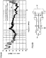
- Fig. 6A shows a result of measurement of the noise level in the power converter according to each of the second embodiment and the comparative example.
- the horizontal axis represents the frequency based on "MHz" as a unit and the vertical axis represents the noise level based on "dB ⁇ V" as a unit.
- a thick solid line bl in Fig. 6A represents the level of noise leaking from external terminal T2 of the power converter according to the second embodiment into negative line 52
- a thin solid line b2 represents the level of noise leaking from external terminal T2 of the power converter according to the comparative example into negative line 52.
- the noise level of the power converter according to the second embodiment is lower than the noise level of the power converter according to the comparative example.
- the decrease of the noise level is attained by inserting inductor 17 into earth line 53. Inductor 17 exhibits the maximum value at 20 MHz.
- the noise level can be reduced by inserting inductor 17 in earth line 53 ( Fig. 4 ).
- inductor 17 in earth line 53 ( Fig. 4 ).
- individual inductors with high versatility can be used, thereby achieving cost reduction.
- a degree of freedom in layout positions of inductors 15, 16, 17 ( Fig. 3 ) becomes high.
- Y capacitors 11, 12 may not be provided.
- inductor 17 inserted between the ground conductor and earth terminal TE serves to suppress the noise generated in the ground conductor from leaking to earth line 53.
- three-phase common mode choke coil 18 is inserted at the input side of power conversion circuit 10 in the first embodiment
- three-phase common mode choke coil 18 is provided at the output side of power conversion circuit 10 in the third embodiment. It should be noted that three-phase common mode choke coils 18 may be inserted both at the input side and the output side.
- Fig. 7 shows an equivalent circuit diagram of the power converter according to the third embodiment.
- a power system 70 is connected to external terminals T3, T4 at the output side of the power converter.
- Earth terminal TE is grounded.
- Two inductors 62 and a capacitor 61 are disposed between nodes N3, N4 at the output side of power conversion circuit 10 and the output node of inverter 30. Two inductors 62 are inserted in respective two output lines of inverter 30. Capacitor 61 connects the two output lines to each other. The capacitor for connecting two signal lines (power supply lines) to each other is commonly referred to as "X capacitor”. X capacitor 61 reduces differential mode noise.
- Inductor 15 is inserted between node N3 and external terminal T3, and inductor 16 is inserted between node N4 and external terminal T4.
- One electrode (first electrode) of a Y capacitor 63 is connected to node N3, and one electrode (first electrode) of a Y capacitor 64 is connected to node N4.
- the other electrode (second electrode) of Y capacitor 63 is connected to the other electrode (second electrode) of Y capacitor 64.
- Inductor 17 is connected between earth terminal TE and interconnection point P2 between Y capacitor 63 and Y capacitor 64.
- Three-phase common mode choke coil 18 is constituted of inductors 15, 16, 17. Furthermore, interconnection point P2 is connected to the ground conductor.
- the level of the common mode noise leaking from external terminals T3, T4 into power system 70 can be reduced. It should be noted that as with the first embodiment shown in Fig. 1 , Y capacitors 63, 64 may not be provided.
- Fig. 8 shows an equivalent circuit diagram of the power converter according to the fourth embodiment. While three-phase common mode choke coil 18 is constituted of inductors 15, 16, 17 ( Fig. 7 ) in the third embodiment, the three inductors, i.e., inductors 15, 16, 17 are independent from one another in the fourth embodiment.
- Fig. 9 shows an equivalent circuit diagram of the power converter according to the fifth embodiment. While the power converter is connected to single-phase power system 70 in the third embodiment, the power converter is connected to a three-phase power system 70 in the fifth embodiment.
- inverter 30 ( Fig. 7 ) of the third embodiment has two switching element pairs
- inverter 30 includes three switching element pairs for U, V, and W phases, and three nodes NU, NV, NW at the output side in the fifth embodiment.
- inverter 30 includes external terminals TU, TV, TW for U, V, and W phases and earth terminal TE. Electrodes (first electrodes) of Y capacitors 19U, 19V, 19W are connected to nodes NU, NV, NW. The other electrodes (second electrodes) of Y capacitors 19U, 19V, 19W are connected to one another.
- a four-phase common mode choke coil 18 is inserted in three power supply lines and an earth line.
- the three power supply lines connect nodes NU, NV, NW to external terminals TU, TV, TW, respectively.
- the earth line connects an interconnection point P3 between the second electrodes of Y capacitors 19U, 19V, 19W to earth terminal TE. Interconnection point P3 is connected to the ground conductor.
- the level of the common mode noise leaking from external terminals TU, TV, TW into power system 70 can be reduced. It should be noted that as with the third embodiment shown in Fig. 7 , Y capacitors 19U, 19V, 19W may not be provided.
Description
- The present invention relates to a power converter.
- A power converter (system interconnection inverter) is used to convert DC power, generated in a photovoltaic power system or the like, into AC power and supply it to a power system. This power converter includes: a boosting converter configured to boost a DC voltage; and an inverter configured to convert the direct current into alternating current. Upon switching of a switching element of the boosting converter, the inverter, or the like, common mode voltage (neutral point potential) is fluctuated.
- A single-phase inverter has an H bridge configuration employing a switching element, and is subjected to 3-level PWM control, for example. Due to this control, common mode voltage is fluctuated. The fluctuation of the common mode voltage causes leakage current flowing to a ground (earth) and high-frequency noise. The high-frequency noise is reduced by inserting a common mode choke coil between a pair of output terminals of a DC power supply and a pair of input terminals of a boosting circuit (see Japanese Patent Laying-Open No.
2011-147238 - A power converter according to the preamble of
claim 1 is known fromDE 10 2013 100246 A1 . - Upon of switching of the switching element of the boosting converter or the inverter, ringing occurs. A conventional common mode choke coil can reduce noise in a low frequency region such as a switching frequency. However, according to various experiments conducted by the inventor of the present application, it was found that the noise reduction effect is low in a high frequency region such as a ringing frequency and a frequency of a harmonic wave thereof.
- The present invention aims to provide a power converter that provides a sufficient noise reduction effect in a high frequency region.
- A power converter according to a first aspect of the present invention comprises:
- a plurality of external terminals;
- an earth terminal connected to a ground;
- a power conversion circuit including a plurality of nodes, each of the plurality of nodes being connected to a corresponding one of the plurality of external terminals, the power conversion circuit being configured to perform power conversion by switching received power;
- a ground conductor;
- a plurality of inductors, each of the plurality of inductors being inserted between a corresponding one of the plurality of external terminals and a corresponding one of the plurality of nodes; and another inductor inserted between the ground conductor and the earth terminal.
- By connecting the inductors to not only the external terminals but also the earth terminal, a noise reduction effect in a high frequency region can be increased.
- Preferably, the power converter further includes a plurality of capacitors each including a first electrode and a second electrode, the first electrode being connected to a corresponding one of the plurality of nodes, the second electrode being connected to the ground conductor.
- Common mode noise appearing in the plurality of nodes flows to the ground conductor via the capacitors.
- Preferably, the plurality of inductors are each inserted between the corresponding one of the plurality of external terminals and the corresponding one of the plurality of nodes are inductively coupled with the other inductor inserted between the ground conductor and the earth terminal to construct a common mode choke coil having not less than three phases.
- By using the common mode choke coil, the noise reduction effect can be increased.
- Preferably, the plurality of external terminals are connected to a DC power supply, and
the power conversion circuit is configured to receive DC power from the plurality of nodes, convert the DC power into AC power and output the AC power. - The common mode noise leaking from the power converter to the DC power supply can be reduced.
- Preferably, the plurality of external terminals are connected to a power system, and
the power conversion circuit is configured to receive DC power, convert the DC power into AC power, and output the converted AC power from the plurality of nodes to the power system. - The common mode noise leaking from the power converter to the power system can be reduced.
- By connecting the inductors to not only the external terminals but also the earth terminal, a noise reduction effect in a high frequency region can be increased.
- The foregoing and other aims, features, aspects and advantages of the present invention will become more apparent from the following detailed description of the present invention when taken in conjunction with the accompanying drawings.
- Embodiments of the invention will now be described, by way of example only, and with reference to the accompanying drawings, in which:
-
Fig. 1 is an equivalent circuit diagram of a power converter according to a first embodiment. - Each of
Fig. 2A and Fig. 2B is an equivalent circuit diagram showing a connection configuration among an external terminal, an earth terminal, and a power conversion circuit of a power converter used in an experiment. -
Fig. 3A is a graph showing a result of measurement of a noise level of the power converter according to each of the first embodiment and a comparative example.Fig. 3B is an equivalent circuit diagram of the power converter according to the comparative example. -
Fig. 4 is an equivalent circuit diagram of a power converter according to a second embodiment. -
Fig. 5A is a graph showing a result of measurement of a transmission property S21 of an inductor used in the power converter according to the second embodiment, andFig. 5B is an equivalent circuit diagram of a two-terminal pair circuit when measuring the transmission property of the inductor. -
Fig. 6A is a graph showing a result of measurement of the noise level of the power converter according to each of the second embodiment and a comparative example, andFig. 6B is an equivalent circuit diagram of the power converter according to the comparative example. -
Fig. 7 is an equivalent circuit diagram of a power converter according to a third embodiment. -
Fig. 8 is an equivalent circuit diagram of a power converter according to a fourth embodiment. -
Fig. 9 is an equivalent circuit diagram of a power converter according to a fifth embodiment. - With reference to
Fig. 1 andFig. 2 , the following describes a power converter according to a first embodiment. -
Fig. 1 shows an equivalent circuit diagram of the power converter according to the first embodiment. The power converter according to the first embodiment includes external terminals T1, T2, an earth terminal TE, a commonmode choke coil 18, and apower conversion circuit 10.Power conversion circuit 10 includes aboosting converter 20 and aninverter 30, and is configured to receive DC power, convert the DC power into AC power, and output the AC power. - External terminals T1 and T2 are connected to positive electrode and negative electrode of a
DC power supply 50 via apositive line 51 and anegative line 52. Earth terminal TE is connected (grounded) to the ground via anearth line 53, and is fixed to the same potential as that of the earth. ForDC power supply 50, a solar panel, a fuel cell, or the like is used, for example. External terminals T1 and T2 are connected to nodes N1 and N2 ofpower conversion circuit 10 via commonmode choke coil 18. - One electrode (first electrode) of a
capacitor 11 is connected to node N1. One electrode (first electrode) of acapacitor 12 is connected to node N2. The other electrode (second electrode) ofcapacitor 11 is connected to the other electrode (second electrode) ofcapacitor 12. A point via which the second electrode ofcapacitor 11 and the second electrode ofcapacitor 12 are connected to each other will be referred to as an interconnection point P1. Interconnection point P1 is connected to a ground conductor ofpower conversion circuit 10. A potential of the ground conductor serves as a reference potential (ground potential) of the power conversion circuit. Generally, a metal housing or the like is used as the ground conductor. Capacitors, such ascapacitors - Common
mode choke coil 18 includes threeinductors mode choke coil 18, ferrite can be used, for example.Inductor 15 is inserted between external terminal T1 and node N1.Inductor 16 is inserted between external terminal T2 and node N2.Inductor 17 is connected between interconnection point P1 and earth terminal TE. Commonmode choke coil 18 is connected such that magnetic fluxes generated by common mode noise current flowing frompower conversion circuit 10 to external terminals T1, T2 and earth terminal TE are intensified with one another. - Boosting
converter 20 includes areactor 21, afree wheel diode 22, and a switchingelement 23.Diode 24 is connected to switchingelement 23 in parallel. An output of boostingconverter 20 is sent toinverter 30. A smoothingcapacitor 40 is connected to a DC line at the output side of boostingconverter 20. -
Inverter 30 includes four switchingelements elements elements - For switching
elements elements - Next, with reference to
Fig. 2A and Fig. 2B , in the power converter according to the first embodiment, the following describes an experiment, based on a result of which three-phase commonmode choke coil 18 is employed. - Each of
Fig. 2A and Fig. 2B shows a connection configuration among external terminals T1, T2, earth terminal TE,power conversion circuit 10, andDC power supply 50 in the power converter used in the experiment. Nodes N1, N2 ofpower conversion circuit 10 are directly connected to external terminals T1, T2, respectively. Interconnection point P1 betweenY capacitors DC power supply 50 viapositive line 51 andnegative line 52, respectively. Earth terminal TE is grounded byearth line 53. - By actually operating the power converter, the level of noise generated from
positive line 51,negative line 52, andearth line 53 was measured using a measuringinstrument 55. - Comparison is made between noise level measured with two lines, i.e.,
positive line 51 andnegative line 52, being interposed by a probe as shown inFig. 2A and noise level measured with three lines, i.e.,positive line 51,negative line 52, andearth line 53, being interposed by a probe as shown inFig. 2B . In a low frequency region of about 100 kHz, the noise level measured by the method ofFig. 2B is lower than the noise level measured by the method ofFig. 2A ; however, in a high frequency region of not less than 1 MHz, there was found no large difference therebetween. - From the result of the experiment shown in
Fig. 2A and Fig. 2B , the following knowledge is obtained. - In the low frequency region of about 100 kHz, it is considered that the noise current flowing through
positive line 51 andnegative line 52 and the noise current flowing throughearth line 53 are opposite in phase (differential mode). On the other hand, in the high frequency region of not less than 1 MHz, it is considered that the noise current flowing throughpositive line 51 andnegative line 52 and the noise current flowing throughearth line 53 are substantially the same in phase (common mode). Therefore, by inserting a three-phase common mode choke coil in the three lines, i.e.,positive line 51,negative line 52, andearth line 53, it is considered possible to reduce the common mode noise in the high frequency region of not less than 1 MHz. - Next, with reference to
Fig. 3A and Fig. 3B , the following describes an excellent effect of the power converter according to the first embodiment. The level of noise generated frompositive line 51,negative line 52, andearth line 53 was measured during an operation of the power converter according to each of the first embodiment and a comparative example. -
Fig. 3B shows an equivalent circuit diagram of the power converter according to the comparative example. In the power converter according to the comparative example, interconnection point P1 ofY capacitors mode choke coil 18. An inductor not used among the three inductors of commonmode choke coil 18 is in an open state. The other configurations are the same as those of the power converter according to the first embodiment. -
Fig. 3A shows a result of measurement of the noise levels of the power converters according to the first embodiment (Fig. 1 ) and the comparative example (Fig. 3B ). The horizontal axis represents the frequency based on "MHz" as a unit and the vertical axis represents the noise level based on "dBµV" as a unit. A thick solid line a1 inFig. 3A represents the level of noise leaking from external terminal T2 of the power converter according to the first embodiment intonegative line 52, and a thin solid line a2 represents the level of noise leaking from external terminal T2 of the power converter according to the comparative example intonegative line 52. - Around a frequency of about 1.2 MHz and 25 MHz, it is understood that noise that is based on ringing resulting from switching has occurred. By employing the configuration of the first embodiment, the noise levels at 1.2 MHz and 25 MHz are decreased as compared with the configuration of the comparative example. Particularly, the decrease of the noise level around the frequency of 25 MHz is remarkable. The decrease of the noise level is attained by inserting three-phase common
mode choke coil 18 inpositive line 51,negative line 52, andearth line 53. - Furthermore, in the first embodiment, an impedance from nodes N1, N2 of
power conversion circuit 10 to the ground point becomes high. Accordingly, leakage current flowing toearth line 53 can be reduced. A direct current flowing throughinductor 15 inserted inpositive line 51 is opposite in direction to a direct current flowing throughinductor 16 inserted innegative line 52. Magnetic fluxes generated by these direct currents serve to cancel each other, whereby magnetic cores ofinductors - In the embodiment shown in
Fig. 1 ,Y capacitors Y capacitors Y capacitors inductor 17 connects the ground conductor to earth terminal TE. By inserting commonmode choke coil 18, the noise propagated from switchingelements positive line 51,negative line 52, andearth line 53. - Next, with reference to
Fig. 4 to Fig. 6A andFig. 6B , the following describes a power converter according to a second embodiment. A difference from the first embodiment will be described and common configurations will not be described. -
Fig. 4 shows an equivalent circuit diagram of the power converter according to the second embodiment. In the first embodiment, three-phase commonmode choke coil 18 is constituted ofinductors Fig. 1 ). In the second embodiment shown inFig. 4 ,inductors inductors - With reference to
Fig. 5A and Fig. 5B , electric properties ofinductors Fig. 5B was constructed usinginductor 15, and a transmission property S21 was measured. -
Fig. 5A shows a result of measurement of transmission property S21. The horizontal axis represents the frequency based on "MHz" as a unit and the vertical axis represents transmission property S21 based on "dB" as a unit. As S21 is smaller, insertion loss is larger. At a frequency of about 20 MHz, insertion loss exhibits the maximum value. - Next, with reference to
Fig. 6A and Fig. 6B , the following describes an excellent effect in the power converter according to the second embodiment. During the operation of each of the power converters according to the second embodiment and a comparative example, the level of noise leaking from external terminal T2 tonegative line 52 was measured. -
Fig. 6B shows an equivalent circuit diagram of the power converter according to the comparative example. In the power converter according to the comparative example, interconnection point P1 betweenY capacitors Fig. 4 ) according to the second embodiment. -
Fig. 6A shows a result of measurement of the noise level in the power converter according to each of the second embodiment and the comparative example. The horizontal axis represents the frequency based on "MHz" as a unit and the vertical axis represents the noise level based on "dBµV" as a unit. A thick solid line bl inFig. 6A represents the level of noise leaking from external terminal T2 of the power converter according to the second embodiment intonegative line 52, and a thin solid line b2 represents the level of noise leaking from external terminal T2 of the power converter according to the comparative example intonegative line 52. - Around a frequency of 20 MHz, it is understood that the noise level of the power converter according to the second embodiment is lower than the noise level of the power converter according to the comparative example. The decrease of the noise level is attained by inserting
inductor 17 intoearth line 53.Inductor 17 exhibits the maximum value at 20 MHz. - As in the second embodiment, the noise level can be reduced by inserting
inductor 17 in earth line 53 (Fig. 4 ). As compared with a case of using three-phase common mode choke coil 18 (Fig. 1 ) of the first embodiment, individual inductors with high versatility can be used, thereby achieving cost reduction. Further, a degree of freedom in layout positions ofinductors Fig. 3 ) becomes high. - Also in the second embodiment, as with the first embodiment shown in
Fig. 1 ,Y capacitors Y capacitors inductor 17 inserted between the ground conductor and earth terminal TE serves to suppress the noise generated in the ground conductor from leaking toearth line 53. - Next, the following describes a power converter according to a third embodiment with reference to
Fig. 7 . Hereinafter, a difference from the first embodiment will be described and common configurations will not be described. While three-phase commonmode choke coil 18 is inserted at the input side ofpower conversion circuit 10 in the first embodiment, three-phase commonmode choke coil 18 is provided at the output side ofpower conversion circuit 10 in the third embodiment. It should be noted that three-phase common mode choke coils 18 may be inserted both at the input side and the output side. -
Fig. 7 shows an equivalent circuit diagram of the power converter according to the third embodiment. Apower system 70 is connected to external terminals T3, T4 at the output side of the power converter. Earth terminal TE is grounded. - Two
inductors 62 and acapacitor 61 are disposed between nodes N3, N4 at the output side ofpower conversion circuit 10 and the output node ofinverter 30. Twoinductors 62 are inserted in respective two output lines ofinverter 30.Capacitor 61 connects the two output lines to each other. The capacitor for connecting two signal lines (power supply lines) to each other is commonly referred to as "X capacitor".X capacitor 61 reduces differential mode noise. -
Inductor 15 is inserted between node N3 and external terminal T3, andinductor 16 is inserted between node N4 and external terminal T4. One electrode (first electrode) of aY capacitor 63 is connected to node N3, and one electrode (first electrode) of aY capacitor 64 is connected to node N4. The other electrode (second electrode) ofY capacitor 63 is connected to the other electrode (second electrode) ofY capacitor 64.Inductor 17 is connected between earth terminal TE and interconnection point P2 betweenY capacitor 63 andY capacitor 64. Three-phase commonmode choke coil 18 is constituted ofinductors - Also in the third embodiment, by inserting three-phase common
mode choke coil 18, the level of the common mode noise leaking from external terminals T3, T4 intopower system 70 can be reduced. It should be noted that as with the first embodiment shown inFig. 1 ,Y capacitors - Next, with reference to
Fig. 8 , the following describes a power converter according to a fourth embodiment. Hereinafter, a difference from the third embodiment (Fig. 7 ) will be described and common configurations will not be described. -
Fig. 8 shows an equivalent circuit diagram of the power converter according to the fourth embodiment. While three-phase commonmode choke coil 18 is constituted ofinductors Fig. 7 ) in the third embodiment, the three inductors, i.e.,inductors - In the fourth embodiment, as with the power converter according to the second embodiment shown in
Fig. 4 , common mode noise can be suppressed from leaking from external terminals T3, T4 topower system 70. It should be noted that as with the third embodiment shown inFig. 7 ,Y capacitors - Next, the following describes a power converter according to a fifth embodiment with reference to
Fig. 9 . Hereinafter, a difference from the third embodiment (Fig. 7 ) will be described and common configurations will not be described. -
Fig. 9 shows an equivalent circuit diagram of the power converter according to the fifth embodiment. While the power converter is connected to single-phase power system 70 in the third embodiment, the power converter is connected to a three-phase power system 70 in the fifth embodiment. - Although inverter 30 (
Fig. 7 ) of the third embodiment has two switching element pairs,inverter 30 includes three switching element pairs for U, V, and W phases, and three nodes NU, NV, NW at the output side in the fifth embodiment. Correspondingly,inverter 30 includes external terminals TU, TV, TW for U, V, and W phases and earth terminal TE. Electrodes (first electrodes) ofY capacitors Y capacitors - A four-phase common
mode choke coil 18 is inserted in three power supply lines and an earth line. The three power supply lines connect nodes NU, NV, NW to external terminals TU, TV, TW, respectively. The earth line connects an interconnection point P3 between the second electrodes ofY capacitors - Also in the fifth embodiment, as with the third embodiment shown in
Fig. 7 , the level of the common mode noise leaking from external terminals TU, TV, TW intopower system 70 can be reduced. It should be noted that as with the third embodiment shown inFig. 7 ,Y capacitors - Each of the above-described embodiments is exemplary and portions of configurations in different embodiments can be replaced or combined. The same function and effect provided by the same configuration among a plurality of embodiments are not described for each of the embodiments. Moreover, the present invention is not limited to the embodiments described above. For example, it is obvious for one having ordinary skill in the art to make various modifications, improvements, combinations, and the like.
- Although the present invention has been described and illustrated in detail, it is clearly understood that the same is by way of illustration and example only and is not to be taken by way of limitation, the scope of the present invention being interpreted by the terms of the appended claims.
Claims (5)
- A power converter comprising:a plurality of external terminals (T1, T2);an earth terminal (TE) connected to a ground;a power conversion circuit (10) including a plurality of nodes (N1, N2), each of the plurality of nodes being connected to a corresponding one of the plurality of external terminals, the power conversion circuit being configured to perform power conversion by switching received power;a ground conductor;a plurality of inductors (15, 16), each of the plurality of inductors being inserted between a corresponding one of the plurality of external terminals and a corresponding one of the plurality of nodes; characterized by another inductor (17) inserted between the ground conductor and the earth terminal.
- The power converter according to claim 1, further comprising a plurality of capacitors (11, 12) each including a first electrode and a second electrode, the first electrode being connected to a corresponding one of the plurality of nodes, the second electrode being connected to the ground conductor.
- The power converter according to claim 1 or 2, wherein the plurality of inductors (15, 16) each inserted between the corresponding one of the plurality of external terminals and the corresponding one of the plurality of nodes are inductively coupled with the another inductor (17) inserted between the ground conductor and the earth terminal to construct a common mode choke coil (18) having not less than three phases.
- The power converter according to any one of claims 1 to 3, wherein
the plurality of external terminals are connected to a DC power supply (50), and
the power conversion circuit is configured to:receive DC power from the plurality of nodes;convert the DC power into AC power; andoutput the AC power. - The power converter according to any one of claims 1 to 3, wherein
the plurality of external terminals are connected to a power system, and
the power conversion circuit is configured to:receive DC power;convert the DC power into AC power; andoutput the converted AC power from the plurality of nodes to the power system.
Applications Claiming Priority (1)
| Application Number | Priority Date | Filing Date | Title |
|---|---|---|---|
| JP2016074140A JP6451681B2 (en) | 2016-04-01 | 2016-04-01 | Power converter |
Publications (2)
| Publication Number | Publication Date |
|---|---|
| EP3229363A1 EP3229363A1 (en) | 2017-10-11 |
| EP3229363B1 true EP3229363B1 (en) | 2018-11-28 |
Family
ID=58228043
Family Applications (1)
| Application Number | Title | Priority Date | Filing Date |
|---|---|---|---|
| EP17159260.3A Active EP3229363B1 (en) | 2016-04-01 | 2017-03-03 | Power converter |
Country Status (4)
| Country | Link |
|---|---|
| US (1) | US9887641B2 (en) |
| EP (1) | EP3229363B1 (en) |
| JP (1) | JP6451681B2 (en) |
| CN (1) | CN107404218B (en) |
Families Citing this family (8)
| Publication number | Priority date | Publication date | Assignee | Title |
|---|---|---|---|---|
| EP3322063B1 (en) * | 2016-11-15 | 2022-04-13 | MARICI Holdings The Netherlands B.V. | A multi-channel inverter for a photovoltaic apparatus |
| JP6832775B2 (en) * | 2017-03-30 | 2021-02-24 | 本田技研工業株式会社 | Engine generator |
| WO2020061902A1 (en) * | 2018-09-27 | 2020-04-02 | Abb Schweiz Ag | Apparatus for conversion between ac power and dc power |
| WO2020061905A1 (en) * | 2018-09-27 | 2020-04-02 | Abb Schweiz Ag | Apparatus for conversion between ac power and dc power |
| WO2020208825A1 (en) * | 2019-04-12 | 2020-10-15 | 三菱電機株式会社 | Power conversion device and air conditioner |
| JP7331946B2 (en) * | 2019-12-17 | 2023-08-23 | 株式会社村田製作所 | electronic circuit |
| US11356011B2 (en) * | 2019-12-19 | 2022-06-07 | University Of Florida Research Foundation, Incorporated | Common mode (CM) electromagnetic interference (EMI) filters for reducing radiated EMI in power converters |
| CN111884500B (en) * | 2020-08-03 | 2022-02-22 | 中车青岛四方车辆研究所有限公司 | Method for suppressing common-mode conducted interference of vehicle-mounted charger |
Family Cites Families (18)
| Publication number | Priority date | Publication date | Assignee | Title |
|---|---|---|---|---|
| JPS6059978A (en) * | 1983-09-12 | 1985-04-06 | Toshiba Corp | Air conditioner |
| US5241217A (en) * | 1991-11-07 | 1993-08-31 | Premier Power, Inc. | UPS with input commutation between AC and DC sources of power |
| JP2001268890A (en) * | 2000-03-16 | 2001-09-28 | Hitachi Ltd | Power converter system |
| JP3778131B2 (en) * | 2002-05-28 | 2006-05-24 | 株式会社日立製作所 | Power conversion system and filter used therefor |
| US6906933B2 (en) * | 2002-11-01 | 2005-06-14 | Powerware Corporation | Power supply apparatus and methods with power-factor correcting bypass mode |
| JP2005287157A (en) * | 2004-03-29 | 2005-10-13 | Mitsubishi Electric Corp | Noise filter and air conditioner |
| CN100365903C (en) * | 2004-11-19 | 2008-01-30 | 艾默生网络能源有限公司 | Single-phase AC inputting electromagnetic interference killer circuit |
| JP4930575B2 (en) * | 2009-11-09 | 2012-05-16 | 三菱電機株式会社 | Noise suppression device, air conditioner |
| JP5468394B2 (en) | 2010-01-13 | 2014-04-09 | 株式会社東芝 | Grid interconnection inverter |
| JP2013162628A (en) | 2012-02-06 | 2013-08-19 | Meidensha Corp | Power generating system, and ground leakage current suppression method of power generating system |
| JP5941376B2 (en) * | 2012-08-29 | 2016-06-29 | 京セラ株式会社 | Power generation control device and power supply system |
| DE102012109638A1 (en) | 2012-10-10 | 2014-05-15 | Sma Solar Technology Ag | Multi-string inverter with input-side EMC filter |
| DE102013100246A1 (en) * | 2013-01-11 | 2014-07-17 | Refusol Gmbh | Current sensor and radio noise filter arrangement for use in transformerless photovoltaic inverter of e.g. power plant, has throttles provided with windings whose winding wire is connected around primary conductors by through-holes |
| US8964432B2 (en) * | 2013-01-29 | 2015-02-24 | The Boeing Company | Apparatus and method for controlling circulating current in an inverter system |
| CN203537229U (en) * | 2013-07-12 | 2014-04-09 | 温岭万顺机电制造有限公司 | EMC common-mode filter circuit applied to electric welding machine |
| US9533638B2 (en) | 2013-07-18 | 2017-01-03 | The Boeing Company | Aircraft universal power converter |
| JP6178178B2 (en) * | 2013-09-09 | 2017-08-09 | 株式会社東芝 | Noise filter |
| JP6191542B2 (en) * | 2014-05-21 | 2017-09-06 | 株式会社デンソー | Power converter |
-
2016
- 2016-04-01 JP JP2016074140A patent/JP6451681B2/en active Active
-
2017
- 2017-03-03 EP EP17159260.3A patent/EP3229363B1/en active Active
- 2017-03-23 US US15/467,565 patent/US9887641B2/en active Active
- 2017-03-30 CN CN201710203778.6A patent/CN107404218B/en active Active
Non-Patent Citations (1)
| Title |
|---|
| None * |
Also Published As
| Publication number | Publication date |
|---|---|
| CN107404218B (en) | 2020-11-17 |
| JP2017188976A (en) | 2017-10-12 |
| US9887641B2 (en) | 2018-02-06 |
| US20170288575A1 (en) | 2017-10-05 |
| CN107404218A (en) | 2017-11-28 |
| EP3229363A1 (en) | 2017-10-11 |
| JP6451681B2 (en) | 2019-01-16 |
Similar Documents
| Publication | Publication Date | Title |
|---|---|---|
| EP3229363B1 (en) | Power converter | |
| US10256739B2 (en) | Multiunit power conversion system | |
| EP3696831B1 (en) | Planar transformer, power source switching circuit and adapter | |
| JP6207751B2 (en) | Power converter | |
| CN110323940B (en) | DC converter, DC converter module and connecting method thereof | |
| EP3734825B1 (en) | Power supply multi-tapped autotransformer | |
| JP2000201044A (en) | Common mode noise reducing device | |
| US9653202B2 (en) | Power converter and device integrating inductors in parallel of the same | |
| US10263537B2 (en) | DC/AC power conversion apparatus having switchable current paths | |
| JP5279381B2 (en) | Power converter | |
| US10090753B1 (en) | Power conversion device and power conversion system | |
| JP5386980B2 (en) | Noise filter | |
| US20220270816A1 (en) | Transformer and switching power supply apparatus for reducing common mode noise due to line-to-ground capacitances | |
| CN213519516U (en) | Three-phase magnetic assembly and integrated core | |
| JP2001197665A (en) | Input line filter | |
| JP4592479B2 (en) | Transformer | |
| JP2008289240A (en) | Active filter device and power conversion equipment | |
| WO2019102937A1 (en) | Noise filter circuit and power supply circuit | |
| US11114932B1 (en) | Method and apparatus for reduction of ripple current | |
| JP2005117218A (en) | Noise suppressing circuit | |
| JP2008079487A (en) | Ac power supply | |
| WO2021106081A1 (en) | Power converter | |
| JP2023179128A (en) | Power output circuit and contactless power feeding system | |
| JP2021191187A (en) | Power conversion device and operation method thereof | |
| JP2022112367A (en) | Choke coil, electrical equipment |
Legal Events
| Date | Code | Title | Description |
|---|---|---|---|
| PUAI | Public reference made under article 153(3) epc to a published international application that has entered the european phase |
Free format text: ORIGINAL CODE: 0009012 |
|
| STAA | Information on the status of an ep patent application or granted ep patent |
Free format text: STATUS: REQUEST FOR EXAMINATION WAS MADE |
|
| 17P | Request for examination filed |
Effective date: 20170630 |
|
| AK | Designated contracting states |
Kind code of ref document: A1 Designated state(s): AL AT BE BG CH CY CZ DE DK EE ES FI FR GB GR HR HU IE IS IT LI LT LU LV MC MK MT NL NO PL PT RO RS SE SI SK SM TR |
|
| AX | Request for extension of the european patent |
Extension state: BA ME |
|
| GRAP | Despatch of communication of intention to grant a patent |
Free format text: ORIGINAL CODE: EPIDOSNIGR1 |
|
| STAA | Information on the status of an ep patent application or granted ep patent |
Free format text: STATUS: GRANT OF PATENT IS INTENDED |
|
| RIC1 | Information provided on ipc code assigned before grant |
Ipc: H02M 7/48 20070101AFI20180524BHEP Ipc: H02M 1/14 20060101ALI20180524BHEP |
|
| INTG | Intention to grant announced |
Effective date: 20180608 |
|
| RIN1 | Information on inventor provided before grant (corrected) |
Inventor name: KITADA, HIROSHI |
|
| GRAS | Grant fee paid |
Free format text: ORIGINAL CODE: EPIDOSNIGR3 |
|
| GRAA | (expected) grant |
Free format text: ORIGINAL CODE: 0009210 |
|
| STAA | Information on the status of an ep patent application or granted ep patent |
Free format text: STATUS: THE PATENT HAS BEEN GRANTED |
|
| AK | Designated contracting states |
Kind code of ref document: B1 Designated state(s): AL AT BE BG CH CY CZ DE DK EE ES FI FR GB GR HR HU IE IS IT LI LT LU LV MC MK MT NL NO PL PT RO RS SE SI SK SM TR |
|
| REG | Reference to a national code |
Ref country code: CH Ref legal event code: EP |
|
| REG | Reference to a national code |
Ref country code: AT Ref legal event code: REF Ref document number: 1071417 Country of ref document: AT Kind code of ref document: T Effective date: 20181215 |
|
| REG | Reference to a national code |
Ref country code: DE Ref legal event code: R096 Ref document number: 602017001031 Country of ref document: DE |
|
| REG | Reference to a national code |
Ref country code: IE Ref legal event code: FG4D |
|
| REG | Reference to a national code |
Ref country code: NL Ref legal event code: MP Effective date: 20181128 |
|
| REG | Reference to a national code |
Ref country code: LT Ref legal event code: MG4D |
|
| REG | Reference to a national code |
Ref country code: AT Ref legal event code: MK05 Ref document number: 1071417 Country of ref document: AT Kind code of ref document: T Effective date: 20181128 |
|
| PG25 | Lapsed in a contracting state [announced via postgrant information from national office to epo] |
Ref country code: BG Free format text: LAPSE BECAUSE OF FAILURE TO SUBMIT A TRANSLATION OF THE DESCRIPTION OR TO PAY THE FEE WITHIN THE PRESCRIBED TIME-LIMIT Effective date: 20190228 Ref country code: NO Free format text: LAPSE BECAUSE OF FAILURE TO SUBMIT A TRANSLATION OF THE DESCRIPTION OR TO PAY THE FEE WITHIN THE PRESCRIBED TIME-LIMIT Effective date: 20190228 Ref country code: LT Free format text: LAPSE BECAUSE OF FAILURE TO SUBMIT A TRANSLATION OF THE DESCRIPTION OR TO PAY THE FEE WITHIN THE PRESCRIBED TIME-LIMIT Effective date: 20181128 Ref country code: HR Free format text: LAPSE BECAUSE OF FAILURE TO SUBMIT A TRANSLATION OF THE DESCRIPTION OR TO PAY THE FEE WITHIN THE PRESCRIBED TIME-LIMIT Effective date: 20181128 Ref country code: AT Free format text: LAPSE BECAUSE OF FAILURE TO SUBMIT A TRANSLATION OF THE DESCRIPTION OR TO PAY THE FEE WITHIN THE PRESCRIBED TIME-LIMIT Effective date: 20181128 Ref country code: IS Free format text: LAPSE BECAUSE OF FAILURE TO SUBMIT A TRANSLATION OF THE DESCRIPTION OR TO PAY THE FEE WITHIN THE PRESCRIBED TIME-LIMIT Effective date: 20190328 Ref country code: LV Free format text: LAPSE BECAUSE OF FAILURE TO SUBMIT A TRANSLATION OF THE DESCRIPTION OR TO PAY THE FEE WITHIN THE PRESCRIBED TIME-LIMIT Effective date: 20181128 Ref country code: FI Free format text: LAPSE BECAUSE OF FAILURE TO SUBMIT A TRANSLATION OF THE DESCRIPTION OR TO PAY THE FEE WITHIN THE PRESCRIBED TIME-LIMIT Effective date: 20181128 |
|
| PG25 | Lapsed in a contracting state [announced via postgrant information from national office to epo] |
Ref country code: GR Free format text: LAPSE BECAUSE OF FAILURE TO SUBMIT A TRANSLATION OF THE DESCRIPTION OR TO PAY THE FEE WITHIN THE PRESCRIBED TIME-LIMIT Effective date: 20190301 Ref country code: AL Free format text: LAPSE BECAUSE OF FAILURE TO SUBMIT A TRANSLATION OF THE DESCRIPTION OR TO PAY THE FEE WITHIN THE PRESCRIBED TIME-LIMIT Effective date: 20181128 Ref country code: SE Free format text: LAPSE BECAUSE OF FAILURE TO SUBMIT A TRANSLATION OF THE DESCRIPTION OR TO PAY THE FEE WITHIN THE PRESCRIBED TIME-LIMIT Effective date: 20181128 Ref country code: RS Free format text: LAPSE BECAUSE OF FAILURE TO SUBMIT A TRANSLATION OF THE DESCRIPTION OR TO PAY THE FEE WITHIN THE PRESCRIBED TIME-LIMIT Effective date: 20181128 Ref country code: PT Free format text: LAPSE BECAUSE OF FAILURE TO SUBMIT A TRANSLATION OF THE DESCRIPTION OR TO PAY THE FEE WITHIN THE PRESCRIBED TIME-LIMIT Effective date: 20190328 |
|
| PG25 | Lapsed in a contracting state [announced via postgrant information from national office to epo] |
Ref country code: NL Free format text: LAPSE BECAUSE OF FAILURE TO SUBMIT A TRANSLATION OF THE DESCRIPTION OR TO PAY THE FEE WITHIN THE PRESCRIBED TIME-LIMIT Effective date: 20181128 |
|
| PG25 | Lapsed in a contracting state [announced via postgrant information from national office to epo] |
Ref country code: IT Free format text: LAPSE BECAUSE OF FAILURE TO SUBMIT A TRANSLATION OF THE DESCRIPTION OR TO PAY THE FEE WITHIN THE PRESCRIBED TIME-LIMIT Effective date: 20181128 Ref country code: PL Free format text: LAPSE BECAUSE OF FAILURE TO SUBMIT A TRANSLATION OF THE DESCRIPTION OR TO PAY THE FEE WITHIN THE PRESCRIBED TIME-LIMIT Effective date: 20181128 Ref country code: DK Free format text: LAPSE BECAUSE OF FAILURE TO SUBMIT A TRANSLATION OF THE DESCRIPTION OR TO PAY THE FEE WITHIN THE PRESCRIBED TIME-LIMIT Effective date: 20181128 Ref country code: ES Free format text: LAPSE BECAUSE OF FAILURE TO SUBMIT A TRANSLATION OF THE DESCRIPTION OR TO PAY THE FEE WITHIN THE PRESCRIBED TIME-LIMIT Effective date: 20181128 Ref country code: CZ Free format text: LAPSE BECAUSE OF FAILURE TO SUBMIT A TRANSLATION OF THE DESCRIPTION OR TO PAY THE FEE WITHIN THE PRESCRIBED TIME-LIMIT Effective date: 20181128 |
|
| REG | Reference to a national code |
Ref country code: DE Ref legal event code: R097 Ref document number: 602017001031 Country of ref document: DE |
|
| PG25 | Lapsed in a contracting state [announced via postgrant information from national office to epo] |
Ref country code: RO Free format text: LAPSE BECAUSE OF FAILURE TO SUBMIT A TRANSLATION OF THE DESCRIPTION OR TO PAY THE FEE WITHIN THE PRESCRIBED TIME-LIMIT Effective date: 20181128 Ref country code: SK Free format text: LAPSE BECAUSE OF FAILURE TO SUBMIT A TRANSLATION OF THE DESCRIPTION OR TO PAY THE FEE WITHIN THE PRESCRIBED TIME-LIMIT Effective date: 20181128 Ref country code: SM Free format text: LAPSE BECAUSE OF FAILURE TO SUBMIT A TRANSLATION OF THE DESCRIPTION OR TO PAY THE FEE WITHIN THE PRESCRIBED TIME-LIMIT Effective date: 20181128 Ref country code: EE Free format text: LAPSE BECAUSE OF FAILURE TO SUBMIT A TRANSLATION OF THE DESCRIPTION OR TO PAY THE FEE WITHIN THE PRESCRIBED TIME-LIMIT Effective date: 20181128 |
|
| PLBE | No opposition filed within time limit |
Free format text: ORIGINAL CODE: 0009261 |
|
| STAA | Information on the status of an ep patent application or granted ep patent |
Free format text: STATUS: NO OPPOSITION FILED WITHIN TIME LIMIT |
|
| PG25 | Lapsed in a contracting state [announced via postgrant information from national office to epo] |
Ref country code: MC Free format text: LAPSE BECAUSE OF FAILURE TO SUBMIT A TRANSLATION OF THE DESCRIPTION OR TO PAY THE FEE WITHIN THE PRESCRIBED TIME-LIMIT Effective date: 20181128 Ref country code: SI Free format text: LAPSE BECAUSE OF FAILURE TO SUBMIT A TRANSLATION OF THE DESCRIPTION OR TO PAY THE FEE WITHIN THE PRESCRIBED TIME-LIMIT Effective date: 20181128 |
|
| 26N | No opposition filed |
Effective date: 20190829 |
|
| PG25 | Lapsed in a contracting state [announced via postgrant information from national office to epo] |
Ref country code: LU Free format text: LAPSE BECAUSE OF NON-PAYMENT OF DUE FEES Effective date: 20190303 |
|
| REG | Reference to a national code |
Ref country code: BE Ref legal event code: MM Effective date: 20190331 |
|
| PG25 | Lapsed in a contracting state [announced via postgrant information from national office to epo] |
Ref country code: IE Free format text: LAPSE BECAUSE OF NON-PAYMENT OF DUE FEES Effective date: 20190303 |
|
| PG25 | Lapsed in a contracting state [announced via postgrant information from national office to epo] |
Ref country code: BE Free format text: LAPSE BECAUSE OF NON-PAYMENT OF DUE FEES Effective date: 20190331 Ref country code: FR Free format text: LAPSE BECAUSE OF NON-PAYMENT OF DUE FEES Effective date: 20190331 |
|
| PG25 | Lapsed in a contracting state [announced via postgrant information from national office to epo] |
Ref country code: TR Free format text: LAPSE BECAUSE OF FAILURE TO SUBMIT A TRANSLATION OF THE DESCRIPTION OR TO PAY THE FEE WITHIN THE PRESCRIBED TIME-LIMIT Effective date: 20181128 |
|
| PG25 | Lapsed in a contracting state [announced via postgrant information from national office to epo] |
Ref country code: MT Free format text: LAPSE BECAUSE OF NON-PAYMENT OF DUE FEES Effective date: 20190303 |
|
| REG | Reference to a national code |
Ref country code: CH Ref legal event code: PL |
|
| PG25 | Lapsed in a contracting state [announced via postgrant information from national office to epo] |
Ref country code: LI Free format text: LAPSE BECAUSE OF NON-PAYMENT OF DUE FEES Effective date: 20200331 Ref country code: CH Free format text: LAPSE BECAUSE OF NON-PAYMENT OF DUE FEES Effective date: 20200331 |
|
| PG25 | Lapsed in a contracting state [announced via postgrant information from national office to epo] |
Ref country code: CY Free format text: LAPSE BECAUSE OF FAILURE TO SUBMIT A TRANSLATION OF THE DESCRIPTION OR TO PAY THE FEE WITHIN THE PRESCRIBED TIME-LIMIT Effective date: 20181128 |
|
| PG25 | Lapsed in a contracting state [announced via postgrant information from national office to epo] |
Ref country code: HU Free format text: LAPSE BECAUSE OF FAILURE TO SUBMIT A TRANSLATION OF THE DESCRIPTION OR TO PAY THE FEE WITHIN THE PRESCRIBED TIME-LIMIT; INVALID AB INITIO Effective date: 20170303 |
|
| GBPC | Gb: european patent ceased through non-payment of renewal fee |
Effective date: 20210303 |
|
| PG25 | Lapsed in a contracting state [announced via postgrant information from national office to epo] |
Ref country code: GB Free format text: LAPSE BECAUSE OF NON-PAYMENT OF DUE FEES Effective date: 20210303 |
|
| PG25 | Lapsed in a contracting state [announced via postgrant information from national office to epo] |
Ref country code: MK Free format text: LAPSE BECAUSE OF FAILURE TO SUBMIT A TRANSLATION OF THE DESCRIPTION OR TO PAY THE FEE WITHIN THE PRESCRIBED TIME-LIMIT Effective date: 20181128 |
|
| PGFP | Annual fee paid to national office [announced via postgrant information from national office to epo] |
Ref country code: DE Payment date: 20230321 Year of fee payment: 7 |