EP3229271A1 - Semiconductor device and liquid discharge head substrate - Google Patents
Semiconductor device and liquid discharge head substrate Download PDFInfo
- Publication number
- EP3229271A1 EP3229271A1 EP17162692.2A EP17162692A EP3229271A1 EP 3229271 A1 EP3229271 A1 EP 3229271A1 EP 17162692 A EP17162692 A EP 17162692A EP 3229271 A1 EP3229271 A1 EP 3229271A1
- Authority
- EP
- European Patent Office
- Prior art keywords
- transistor
- terminal
- voltage
- insulating film
- primary terminal
- Prior art date
- Legal status (The legal status is an assumption and is not a legal conclusion. Google has not performed a legal analysis and makes no representation as to the accuracy of the status listed.)
- Granted
Links
Images


Classifications
-
- B—PERFORMING OPERATIONS; TRANSPORTING
- B41—PRINTING; LINING MACHINES; TYPEWRITERS; STAMPS
- B41J—TYPEWRITERS; SELECTIVE PRINTING MECHANISMS, i.e. MECHANISMS PRINTING OTHERWISE THAN FROM A FORME; CORRECTION OF TYPOGRAPHICAL ERRORS
- B41J2/00—Typewriters or selective printing mechanisms characterised by the printing or marking process for which they are designed
- B41J2/005—Typewriters or selective printing mechanisms characterised by the printing or marking process for which they are designed characterised by bringing liquid or particles selectively into contact with a printing material
- B41J2/01—Ink jet
- B41J2/135—Nozzles
- B41J2/14—Structure thereof only for on-demand ink jet heads
-
- H—ELECTRICITY
- H10—SEMICONDUCTOR DEVICES; ELECTRIC SOLID-STATE DEVICES NOT OTHERWISE PROVIDED FOR
- H10P—GENERIC PROCESSES OR APPARATUS FOR THE MANUFACTURE OR TREATMENT OF DEVICES COVERED BY CLASS H10
- H10P74/00—Testing or measuring during manufacture or treatment of wafers, substrates or devices
-
- H—ELECTRICITY
- H10—SEMICONDUCTOR DEVICES; ELECTRIC SOLID-STATE DEVICES NOT OTHERWISE PROVIDED FOR
- H10D—INORGANIC ELECTRIC SEMICONDUCTOR DEVICES
- H10D89/00—Aspects of integrated devices not covered by groups H10D84/00 - H10D88/00
- H10D89/60—Integrated devices comprising arrangements for electrical or thermal protection, e.g. protection circuits against electrostatic discharge [ESD]
- H10D89/601—Integrated devices comprising arrangements for electrical or thermal protection, e.g. protection circuits against electrostatic discharge [ESD] for devices having insulated gate electrodes, e.g. for IGFETs or IGBTs
- H10D89/811—Integrated devices comprising arrangements for electrical or thermal protection, e.g. protection circuits against electrostatic discharge [ESD] for devices having insulated gate electrodes, e.g. for IGFETs or IGBTs using FETs as protective elements
-
- H—ELECTRICITY
- H10—SEMICONDUCTOR DEVICES; ELECTRIC SOLID-STATE DEVICES NOT OTHERWISE PROVIDED FOR
- H10D—INORGANIC ELECTRIC SEMICONDUCTOR DEVICES
- H10D48/00—Individual devices not covered by groups H10D1/00 - H10D44/00
- H10D48/30—Devices controlled by electric currents or voltages
-
- B—PERFORMING OPERATIONS; TRANSPORTING
- B41—PRINTING; LINING MACHINES; TYPEWRITERS; STAMPS
- B41J—TYPEWRITERS; SELECTIVE PRINTING MECHANISMS, i.e. MECHANISMS PRINTING OTHERWISE THAN FROM A FORME; CORRECTION OF TYPOGRAPHICAL ERRORS
- B41J2/00—Typewriters or selective printing mechanisms characterised by the printing or marking process for which they are designed
- B41J2/005—Typewriters or selective printing mechanisms characterised by the printing or marking process for which they are designed characterised by bringing liquid or particles selectively into contact with a printing material
- B41J2/01—Ink jet
- B41J2/015—Ink jet characterised by the jet generation process
- B41J2/04—Ink jet characterised by the jet generation process generating single droplets or particles on demand
- B41J2/045—Ink jet characterised by the jet generation process generating single droplets or particles on demand by pressure, e.g. electromechanical transducers
- B41J2/04501—Control methods or devices therefor, e.g. driver circuits, control circuits
- B41J2/04511—Control methods or devices therefor, e.g. driver circuits, control circuits for electrostatic discharge protection
-
- B—PERFORMING OPERATIONS; TRANSPORTING
- B41—PRINTING; LINING MACHINES; TYPEWRITERS; STAMPS
- B41J—TYPEWRITERS; SELECTIVE PRINTING MECHANISMS, i.e. MECHANISMS PRINTING OTHERWISE THAN FROM A FORME; CORRECTION OF TYPOGRAPHICAL ERRORS
- B41J2/00—Typewriters or selective printing mechanisms characterised by the printing or marking process for which they are designed
- B41J2/005—Typewriters or selective printing mechanisms characterised by the printing or marking process for which they are designed characterised by bringing liquid or particles selectively into contact with a printing material
- B41J2/01—Ink jet
- B41J2/015—Ink jet characterised by the jet generation process
- B41J2/04—Ink jet characterised by the jet generation process generating single droplets or particles on demand
- B41J2/045—Ink jet characterised by the jet generation process generating single droplets or particles on demand by pressure, e.g. electromechanical transducers
- B41J2/04501—Control methods or devices therefor, e.g. driver circuits, control circuits
- B41J2/04541—Specific driving circuit
-
- B—PERFORMING OPERATIONS; TRANSPORTING
- B41—PRINTING; LINING MACHINES; TYPEWRITERS; STAMPS
- B41J—TYPEWRITERS; SELECTIVE PRINTING MECHANISMS, i.e. MECHANISMS PRINTING OTHERWISE THAN FROM A FORME; CORRECTION OF TYPOGRAPHICAL ERRORS
- B41J2/00—Typewriters or selective printing mechanisms characterised by the printing or marking process for which they are designed
- B41J2/005—Typewriters or selective printing mechanisms characterised by the printing or marking process for which they are designed characterised by bringing liquid or particles selectively into contact with a printing material
- B41J2/01—Ink jet
- B41J2/015—Ink jet characterised by the jet generation process
- B41J2/04—Ink jet characterised by the jet generation process generating single droplets or particles on demand
- B41J2/045—Ink jet characterised by the jet generation process generating single droplets or particles on demand by pressure, e.g. electromechanical transducers
- B41J2/04501—Control methods or devices therefor, e.g. driver circuits, control circuits
- B41J2/0458—Control methods or devices therefor, e.g. driver circuits, control circuits controlling heads based on heating elements forming bubbles
-
- B—PERFORMING OPERATIONS; TRANSPORTING
- B41—PRINTING; LINING MACHINES; TYPEWRITERS; STAMPS
- B41J—TYPEWRITERS; SELECTIVE PRINTING MECHANISMS, i.e. MECHANISMS PRINTING OTHERWISE THAN FROM A FORME; CORRECTION OF TYPOGRAPHICAL ERRORS
- B41J2/00—Typewriters or selective printing mechanisms characterised by the printing or marking process for which they are designed
- B41J2/005—Typewriters or selective printing mechanisms characterised by the printing or marking process for which they are designed characterised by bringing liquid or particles selectively into contact with a printing material
- B41J2/01—Ink jet
- B41J2/135—Nozzles
- B41J2/14—Structure thereof only for on-demand ink jet heads
- B41J2/14016—Structure of bubble jet print heads
- B41J2/14072—Electrical connections, e.g. details on electrodes, connecting the chip to the outside...
-
- H—ELECTRICITY
- H02—GENERATION; CONVERSION OR DISTRIBUTION OF ELECTRIC POWER
- H02H—EMERGENCY PROTECTIVE CIRCUIT ARRANGEMENTS
- H02H9/00—Emergency protective circuit arrangements for limiting excess current or voltage without disconnection
- H02H9/04—Emergency protective circuit arrangements for limiting excess current or voltage without disconnection responsive to excess voltage
- H02H9/045—Emergency protective circuit arrangements for limiting excess current or voltage without disconnection responsive to excess voltage adapted to a particular application and not provided for elsewhere
-
- H—ELECTRICITY
- H10—SEMICONDUCTOR DEVICES; ELECTRIC SOLID-STATE DEVICES NOT OTHERWISE PROVIDED FOR
- H10D—INORGANIC ELECTRIC SEMICONDUCTOR DEVICES
- H10D84/00—Integrated devices formed in or on semiconductor substrates that comprise only semiconducting layers, e.g. on Si wafers or on GaAs-on-Si wafers
- H10D84/01—Manufacture or treatment
- H10D84/0123—Integrating together multiple components covered by H10D12/00 or H10D30/00, e.g. integrating multiple IGBTs
- H10D84/0126—Integrating together multiple components covered by H10D12/00 or H10D30/00, e.g. integrating multiple IGBTs the components including insulated gates, e.g. IGFETs
-
- H—ELECTRICITY
- H10—SEMICONDUCTOR DEVICES; ELECTRIC SOLID-STATE DEVICES NOT OTHERWISE PROVIDED FOR
- H10D—INORGANIC ELECTRIC SEMICONDUCTOR DEVICES
- H10D84/00—Integrated devices formed in or on semiconductor substrates that comprise only semiconducting layers, e.g. on Si wafers or on GaAs-on-Si wafers
- H10D84/80—Integrated devices formed in or on semiconductor substrates that comprise only semiconducting layers, e.g. on Si wafers or on GaAs-on-Si wafers characterised by the integration of at least one component covered by groups H10D12/00 or H10D30/00, e.g. integration of IGFETs
- H10D84/82—Integrated devices formed in or on semiconductor substrates that comprise only semiconducting layers, e.g. on Si wafers or on GaAs-on-Si wafers characterised by the integration of at least one component covered by groups H10D12/00 or H10D30/00, e.g. integration of IGFETs of only field-effect components
- H10D84/83—Integrated devices formed in or on semiconductor substrates that comprise only semiconducting layers, e.g. on Si wafers or on GaAs-on-Si wafers characterised by the integration of at least one component covered by groups H10D12/00 or H10D30/00, e.g. integration of IGFETs of only field-effect components of only insulated-gate FETs [IGFET]
-
- H—ELECTRICITY
- H10—SEMICONDUCTOR DEVICES; ELECTRIC SOLID-STATE DEVICES NOT OTHERWISE PROVIDED FOR
- H10D—INORGANIC ELECTRIC SEMICONDUCTOR DEVICES
- H10D89/00—Aspects of integrated devices not covered by groups H10D84/00 - H10D88/00
- H10D89/60—Integrated devices comprising arrangements for electrical or thermal protection, e.g. protection circuits against electrostatic discharge [ESD]
- H10D89/601—Integrated devices comprising arrangements for electrical or thermal protection, e.g. protection circuits against electrostatic discharge [ESD] for devices having insulated gate electrodes, e.g. for IGFETs or IGBTs
- H10D89/811—Integrated devices comprising arrangements for electrical or thermal protection, e.g. protection circuits against electrostatic discharge [ESD] for devices having insulated gate electrodes, e.g. for IGFETs or IGBTs using FETs as protective elements
- H10D89/817—FETs in a Darlington configuration
-
- H—ELECTRICITY
- H10—SEMICONDUCTOR DEVICES; ELECTRIC SOLID-STATE DEVICES NOT OTHERWISE PROVIDED FOR
- H10D—INORGANIC ELECTRIC SEMICONDUCTOR DEVICES
- H10D89/00—Aspects of integrated devices not covered by groups H10D84/00 - H10D88/00
- H10D89/60—Integrated devices comprising arrangements for electrical or thermal protection, e.g. protection circuits against electrostatic discharge [ESD]
- H10D89/601—Integrated devices comprising arrangements for electrical or thermal protection, e.g. protection circuits against electrostatic discharge [ESD] for devices having insulated gate electrodes, e.g. for IGFETs or IGBTs
- H10D89/811—Integrated devices comprising arrangements for electrical or thermal protection, e.g. protection circuits against electrostatic discharge [ESD] for devices having insulated gate electrodes, e.g. for IGFETs or IGBTs using FETs as protective elements
- H10D89/819—Bias arrangements for gate electrodes of FETs, e.g. RC networks or voltage partitioning circuits
-
- H—ELECTRICITY
- H10—SEMICONDUCTOR DEVICES; ELECTRIC SOLID-STATE DEVICES NOT OTHERWISE PROVIDED FOR
- H10D—INORGANIC ELECTRIC SEMICONDUCTOR DEVICES
- H10D89/00—Aspects of integrated devices not covered by groups H10D84/00 - H10D88/00
- H10D89/60—Integrated devices comprising arrangements for electrical or thermal protection, e.g. protection circuits against electrostatic discharge [ESD]
- H10D89/601—Integrated devices comprising arrangements for electrical or thermal protection, e.g. protection circuits against electrostatic discharge [ESD] for devices having insulated gate electrodes, e.g. for IGFETs or IGBTs
- H10D89/911—Integrated devices comprising arrangements for electrical or thermal protection, e.g. protection circuits against electrostatic discharge [ESD] for devices having insulated gate electrodes, e.g. for IGFETs or IGBTs using passive elements as protective elements
-
- H—ELECTRICITY
- H10—SEMICONDUCTOR DEVICES; ELECTRIC SOLID-STATE DEVICES NOT OTHERWISE PROVIDED FOR
- H10D—INORGANIC ELECTRIC SEMICONDUCTOR DEVICES
- H10D89/00—Aspects of integrated devices not covered by groups H10D84/00 - H10D88/00
- H10D89/60—Integrated devices comprising arrangements for electrical or thermal protection, e.g. protection circuits against electrostatic discharge [ESD]
- H10D89/601—Integrated devices comprising arrangements for electrical or thermal protection, e.g. protection circuits against electrostatic discharge [ESD] for devices having insulated gate electrodes, e.g. for IGFETs or IGBTs
- H10D89/921—Integrated devices comprising arrangements for electrical or thermal protection, e.g. protection circuits against electrostatic discharge [ESD] for devices having insulated gate electrodes, e.g. for IGFETs or IGBTs characterised by the configuration of the interconnections connecting the protective arrangements, e.g. ESD buses
-
- H—ELECTRICITY
- H10—SEMICONDUCTOR DEVICES; ELECTRIC SOLID-STATE DEVICES NOT OTHERWISE PROVIDED FOR
- H10D—INORGANIC ELECTRIC SEMICONDUCTOR DEVICES
- H10D89/00—Aspects of integrated devices not covered by groups H10D84/00 - H10D88/00
- H10D89/60—Integrated devices comprising arrangements for electrical or thermal protection, e.g. protection circuits against electrostatic discharge [ESD]
- H10D89/601—Integrated devices comprising arrangements for electrical or thermal protection, e.g. protection circuits against electrostatic discharge [ESD] for devices having insulated gate electrodes, e.g. for IGFETs or IGBTs
- H10D89/931—Integrated devices comprising arrangements for electrical or thermal protection, e.g. protection circuits against electrostatic discharge [ESD] for devices having insulated gate electrodes, e.g. for IGFETs or IGBTs characterised by the dispositions of the protective arrangements
-
- B—PERFORMING OPERATIONS; TRANSPORTING
- B41—PRINTING; LINING MACHINES; TYPEWRITERS; STAMPS
- B41J—TYPEWRITERS; SELECTIVE PRINTING MECHANISMS, i.e. MECHANISMS PRINTING OTHERWISE THAN FROM A FORME; CORRECTION OF TYPOGRAPHICAL ERRORS
- B41J2202/00—Embodiments of or processes related to ink-jet or thermal heads
- B41J2202/01—Embodiments of or processes related to ink-jet heads
- B41J2202/13—Heads having an integrated circuit
-
- H—ELECTRICITY
- H10—SEMICONDUCTOR DEVICES; ELECTRIC SOLID-STATE DEVICES NOT OTHERWISE PROVIDED FOR
- H10D—INORGANIC ELECTRIC SEMICONDUCTOR DEVICES
- H10D30/00—Field-effect transistors [FET]
- H10D30/60—Insulated-gate field-effect transistors [IGFET]
- H10D30/64—Double-diffused metal-oxide semiconductor [DMOS] FETs
- H10D30/65—Lateral DMOS [LDMOS] FETs
-
- H—ELECTRICITY
- H10—SEMICONDUCTOR DEVICES; ELECTRIC SOLID-STATE DEVICES NOT OTHERWISE PROVIDED FOR
- H10W—GENERIC PACKAGES, INTERCONNECTIONS, CONNECTORS OR OTHER CONSTRUCTIONAL DETAILS OF DEVICES COVERED BY CLASS H10
- H10W10/00—Isolation regions in semiconductor bodies between components of integrated devices
- H10W10/01—Manufacture or treatment
- H10W10/011—Manufacture or treatment of isolation regions comprising dielectric materials
- H10W10/012—Manufacture or treatment of isolation regions comprising dielectric materials using local oxidation of silicon [LOCOS]
-
- H—ELECTRICITY
- H10—SEMICONDUCTOR DEVICES; ELECTRIC SOLID-STATE DEVICES NOT OTHERWISE PROVIDED FOR
- H10W—GENERIC PACKAGES, INTERCONNECTIONS, CONNECTORS OR OTHER CONSTRUCTIONAL DETAILS OF DEVICES COVERED BY CLASS H10
- H10W10/00—Isolation regions in semiconductor bodies between components of integrated devices
- H10W10/10—Isolation regions comprising dielectric materials
- H10W10/13—Isolation regions comprising dielectric materials formed using local oxidation of silicon [LOCOS], e.g. sealed interface localised oxidation [SILO] or side-wall mask isolation [SWAMI]
Definitions
- the present invention relates to a semiconductor device and a liquid discharge head substrate.
- Japanese Patent Laid-Open No. 10-209292 discloses a protection circuit for protecting an element from ESD (Electro-Static Discharge: ESD) in a semiconductor device.
- the protection circuit in Japanese Patent Laid-Open No. 10-209292 includes a transistor M2 which connects a voltage line and a ground line. If a surge voltage is generated in the voltage line, the transistor M2 is turned on, and a current flows from the voltage line to the ground line, discharging the surge voltage in the voltage line.
- Japanese Patent Laid-Open No. 10-20929292 discloses that an internal circuit is protected from ESD as a result.
- capacitive coupling for transmitting the voltage fluctuations to the gate of the transistor M1 may be lacking if only a gate-drain parasitic capacitance of a MOS is used as a capacitive element in the protection circuit.
- a gate-source capacitance of the transistor M1 cannot be charged, and thus it may be impossible to sufficiently secure a gate-source voltage Vgs for turning on the transistor M1. As a result, the function of the protection circuit may be degraded.
- Japanese Patent Laid-Open No. 10-209292 discloses additional use of the capacitive element. However, it does not disclose the concrete structure of the capacitive element. In order to use it for a high-voltage terminal, the high breakdown voltage of the capacitive element is required.
- an oxide film capacitance obtained by thickening a gate oxide film or a pn-junction capacitance utilizing a pn-junction can be used as the capacitive element in the protection circuit.
- a process of forming a thick oxide film is needed, increasing the number of steps in the process.
- the pn-junction capacitance is poor in area efficiency, increasing cost.
- the present invention provides a technique advantageous in appropriately protecting an internal circuit from ESD in a semiconductor device.
- the present invention in its first aspect provides a semiconductor device as specified in claims 1 to 9.
- the present invention in its second aspect provide a liquid discharge head substrate as specified in claims 10 to 14.
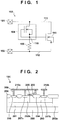
- Fig. 1 is a circuit diagram showing the circuit arrangement of a semiconductor device 100 according to a first embodiment of the present invention.
- the semiconductor device 100 forms a protection circuit for protecting an internal circuit from Electro-Static Discharge (ESD).
- the semiconductor device 100 includes a transistor 103, a transistor 104, and a resistive element 105.
- One primary terminal (drain) of the transistor 103 and one primary terminal (drain) of the transistor 104 are connected to a voltage line 111.
- the other primary terminal (source) of the transistor 103 and one terminal of the resistive element 105 is connected to a voltage line 112.
- the control terminal (gate) of the transistor 103, the control terminal (gate) and the other primary terminal (source) of the transistor 104, and the other terminal of the resistive element 105 are connected to each other so as to form one node 110.
- a high voltage V H is supplied from a terminal 101 to the voltage line 111, and a ground potential is supplied from a terminal 102 to the voltage line 112.
- DMOS Double-Diffused MOS transistors each serving as a high-voltage tolerant element having a higher breakdown voltage than an ordinary transistor are used for the transistor 103 and the transistor 104.
- Fig. 2 shows the sectional structure of the transistor 104 surrounded by a dotted line in Fig. 1 .
- a buried layer 201 serving as an n-type semiconductor region and a well region 202a serving as a p-type semiconductor region are arranged in a p-type semiconductor region 200.
- the semiconductor region 200 may be, for example, a p-type semiconductor substrate of silicon or the like, or a p-type well region formed on a substrate. In this embodiment, a p-type semiconductor substrate of silicon is used for the semiconductor region 200.
- a well region 202b serving as a p-type semiconductor region and a well region 203 serving as an n-type semiconductor region are arranged on the buried layer 201.
- a gate electrode 206 is arranged above the well region 202b and the well region 203 through a gate insulating film 205.
- the gate electrode 206 includes portions arranged on the well region 202b, the well region 203, and a field insulating film 204, respectively. Accordingly, the substantial gate insulating film thickness of a portion contacting the well region 203 on the gate insulating film 205 and the field insulating film 204 is thicker than the gate insulating film thickness of a portion contacting the well regions 202b and 203 only on the gate insulating film 205.
- the gate insulating film 205 may use, for example, silicon oxide, silicon nitride, silicon oxynitride, or the like.
- the gate electrode 206 may be formed by using, for example, polysilicon.
- Diffusion regions 207a and 207b are n-type high-concentration diffusion regions.
- a diffusion region 208 is a p-type high-concentration diffusion region.
- the diffusion regions 207a, 207b, and 208 form respective electrodes (terminals) of a source, a drain, and a back gate, respectively as will be described later.
- the gate electrode 206 and the diffusion regions 207a, 207b, and 208 are electrically connected to wirings 210a and 210b, respectively, via contact portions 209.
- a metal or the like is used for the contact portions 209 and the wirings 210a and 210b.
- the field insulating films 204 each having a LOCOS (LOCal Oxidation of Silicon) structure are arranged between the respective electrodes and between the elements such as the transistors or the like.
- Each field insulating film 204 may have an STI (Shallow Trench Isolation) structure.
- the conductivity types of semiconductors described above including the conductivity types of semiconductors to be described later may be opposite from each other.
- the gate electrode 206 is arranged above the well region 202b and the well region 203 adjacent to each other through the gate insulating film 205. A region in which the well region 202b and the gate electrode 206 overlap becomes a channel region.
- the transistor 104 is an LDMOS (Laterally Diffused MOS) transistor that is a lateral DMOS with the channel region being formed along the surface of the semiconductor substrate, as shown in Fig. 2 .
- the diffusion region 207a forms a source electrode (source region), and the diffusion region 208 forms a back gate electrode. As shown in Figs. 1 and 2 , the source electrode and the gate electrode 206 of the transistor 104 are short-circuited.
- the well region 203 functions as an electric field relaxation region in the drain region and extends below the gate electrode 206.
- the diffusion region 207b formed in the well region 203 forms a drain electrode (drain region).
- the n-type well region 203 is lower in impurity concentration than the diffusion region 207b having the same n conductivity type.
- the field insulating film 204 is arranged on the well region 203.
- the drain side of the gate electrode 206 has a structure which extends on the field insulating film 204, that is, a so-called LOCOS offset structure.
- the transistor 103 may also have the same arrangement as the transistor 104. However, it differs in arrangement of the wirings 210a and 210b, and the gate electrode 206 and the source electrode are not short-circuited.
- the gate insulating film 205 and the field insulating films 204 may be formed by the same material.
- the gate insulating film 205 and the field insulating films 204 may be formed in different processes. However, their structures include insulating films formed by the same material and having portions different in thickness.
- Pn-junction parasitic capacitances C ds1 exist between the well region 202b and the well region 203, and between the well region 202b and the buried layer 201.
- a parasitic capacitance C gd1 exists between the well region 203 and the gate electrode 206.
- a parasitic capacitance C gs1 exists between the well region 202b and the gate electrode 206.
- the operation of the semiconductor device 100 shown in Fig. 1 will now be described.
- a state before a high surge voltage is applied, by ESD, from the terminal 101 to the voltage line 111 at high speed will be considered.
- the parasitic capacitances C gd1 and C ds1 of the transistor 104 do not transmit a low-frequency signal, and thus the gate potential of the transistor 103 becomes a ground potential of 0 V. Consequently, the transistor 103 is turned off, and no current flows between the source and drain of the transistor 103.
- a case will now be considered in which the high surge voltage is applied, by ESD, from the terminal 101 to the voltage line 111 at high speed.
- the parasitic capacitances C gd1 and C ds1 of the transistor 104 exist in series to a parasitic capacitance C gs2 which exists between the source electrode and the gate electrode of the transistor 103, and these capacitances undergo capacitive coupling and work as coupling capacitances.
- a parasitic capacitance C gd2 which exists between the gate electrode and the drain electrode of the transistor 103 also exists in parallel to the parasitic capacitances C gd1 and C ds1 of the transistor 104, and thus these capacitances undergo capacitive coupling and work as coupling capacitances.
- the parasitic capacitances C gd1 , C ds1 , and C gd2 charge the gate-source parasitic capacitance C gs2 of the transistor 103 and turns on the transistor 103. That is, when the surge voltage is applied to the drain of the transistor 104, a potential change in the drain of the transistor 104 is transmitted to the gate electrode of the transistor 103 by capacitive coupling between the node 110 and the drain of the transistor 104. As a result, the transistor 103 is turned on, and a surge current flows through the terminal 102 via the voltage line 112, preventing the surge current from flowing through the internal circuit.
- Each of the parasitic capacitances C gd1 , C gs1 , and C ds1 has voltage dependence. Therefore, if a surge voltage V sur to be applied is high, a depletion layer of each parasitic capacitance C ds1 becomes thick, and the parasitic capacitance C gd1 loses its effect. When the surge voltage rises, however, the voltage dependence of each parasitic capacitance C ds1 is weak. Therefore, the depletion layer of each parasitic capacitance C ds1 is thin, and the parasitic capacitance C gd1 has its effect.
- V gs C ds 1 + C gd 1 + C gd 2 C ds 1 + C gd 1 + C gd 2 + C gs 2 ⁇ V sur
- the respective values of the parasitic capacitances C gd1 , C gs1 , C gd2 , and C gs2 are decided such that the surge current can flow sufficiently. More specifically, the respective values of the parasitic capacitances C gd1 , C gs1 , C gd2 , and C gs2 can be decided by deciding the gate lengths and the gate widths of the transistors 103 and 104 appropriately. Then, the time during which the transistor 103 is ON is adjusted by selecting the resistive value of the resistive element 105 appropriately.
- a capacitance required for the semiconductor device 100 is implemented by a parasitic capacitance, eliminating the need to add a capacitive element or the like.
- a high breakdown voltage is required of a capacitance element used for a protection circuit to which a high voltage like ESD is applied.
- a MOS capacitance, a pn-junction capacitance utilizing a p-n junction, or the like can be used as the capacitive element of the protection circuit.
- the MOS capacitance is used as the capacitive element, an insulating film thicker than other transistors included in the internal circuit or the like needs to be formed in order to make a breakdown voltage higher than those of the other transistors.
- This requires, for example, an additional step of forming the thick insulating film in addition to a step of forming the gate insulating film of a transistor, incurring the possibility of increasing the number of steps in a manufacturing process.
- the pn-junction capacitance is poor in area efficiency, making it difficult to downsize the semiconductor device.
- the semiconductor device 100 described in this embodiment functions as a capacitance by innovating the connection of the transistor 103. It is therefore possible to arrange a capacitive element having a large capacitive value without adding the capacitive element. As a result, an increase in the number of steps in the manufacturing process can be suppressed, and further the area efficiency can also be improved.
- Fig. 3 is a circuit diagram showing the circuit arrangement of a semiconductor device 300 according to a second embodiment of the present invention.
- the semiconductor device 300 includes a capacitance element Ca which forms an anti-fuse element, and transistors 103 and 104 and a resistive element 105 each having the same arrangement as the above-described semiconductor device 100 as a protection circuit which protects the anti-fuse element.
- the semiconductor device 300 also includes a transistor MD1, a transistor MP1, a transistor MN1, and a resistive element Rp.
- Fig. 3 shows a state before information is written in the anti-fuse element, in other words, before the capacitance element Ca is broken.
- the transistor MP1 is a p-type MOS transistor, and the transistor MN1 is an n-type MOS transistor.
- the transistors MP1 and MN1 use ordinary MOS transistors, and are lower in breakdown voltage than DMOS transistors used for the transistors 103 and 104. In other words, the transistors 103 and 104 are higher in breakdown voltage than the transistors MP1 and MN1.
- the transistor MD1 is a DMOS transistor like the transistors 103 and 104, and higher in breakdown voltage than the transistors MP1 and MN1, a detail of which will be described later.
- the back gate and one primary terminal (source) of the transistor MP1 are connected to a logic power supply voltage V DD .
- the back gate and one primary terminal (source) of the transistor MN1 are connected to a voltage line 112.
- the logic power supply voltage V DD is lower in potential than a high voltage V H supplied to a terminal 101.
- the voltage line 112 is connected to a terminal 102 and a ground potential as described above.
- a control signal Sig is input to the control electrode (gate) of the transistor MP1 and the control electrode (gate) of the transistor MN1.
- the other primary terminal (drain) of the transistor MP1 and the other primary terminal (drain) of the transistor MN1 are connected to each other, and form an inverter circuit serving as a driving unit by the transistor MP1 and the transistor MN1.
- a control signal Vg serving as an output signal of the inverter circuit (driving unit) is input to the control electrode (gate) of the transistor MD1 which controls the write in the anti-fuse element.
- the back gate and one primary electrode (source) of the transistor MD1 are connected to the voltage line 112.
- the other primary terminal (drain) of the transistor MD1 is connected to one terminal of the capacitance element Ca which forms the anti-fuse element.
- the other terminal of the capacitance element Ca is connected to a voltage line 111.
- the high voltage V H applied when the information is written in the anti-fuse element is supplied from the terminal 101 to the voltage line 111.
- One terminal of the resistive element Rp is connected to the drain of the transistor MD1 and one terminal of the capacitance element Ca so as to form one node.
- the other terminal of the resistive element Rp is connected to the voltage line 111.
- Fig. 4 shows the sectional structure of the capacitance element Ca and the transistor MD1 surrounded by a dotted line shown in Fig. 3 .
- a well region 301 serving as a p-type semiconductor region, and well regions 302a and 302b each serving as an n-type semiconductor region are arranged on a p-type semiconductor region 310.
- a p-type semiconductor substrate of silicon is used for the semiconductor region 310.
- the well region 301 has a common impurity concentration with a p-type well region of the transistor MN1 which forms a logic circuit of the driving unit.
- Each of the well regions 302a and 302b has a common impurity concentration with an n-type well region of the transistor MP1 which forms a logic circuit of the driving unit. Note that the impurity concentrations of the well regions 302a and 302b need to be set with respect to the impurity concentration of the semiconductor region 310 such that a breakdown voltage between the semiconductor region 310, and the well regions 302a and 302b becomes higher than the high voltage V H .
- a field insulating film 303 has a LOCOS structure.
- a gate insulating film 304 of the transistor MD1 uses, for example, silicon oxide, and is formed simultaneously with a step of forming the gate insulating films of the transistors MP1 and MN1 each forming the logic circuit of the driving unit.
- the capacitance element Ca which forms the anti-fuse element has a MOS structure, and the gate insulating film 304 which forms this capacitance element Ca is also formed simultaneously with the gate insulating films of the transistors MD1, MP1, and MN1.
- a gate electrode 305a is the gate electrode of the transistor MD1, and a gate electrode 305b is an electrode which forms the other terminal of the capacitance element Ca serving as the anti-fuse element.
- the gate electrodes 305a and 305b are formed by using, for example, polysilicon.
- Diffusion regions 306a to 306c are n-type high-concentration diffusion regions.
- a diffusion region 307 is a p-type high-concentration diffusion region.
- the gate electrodes 305a and 305b, and the diffusion regions 306a to 306c and 307 can be formed in the same step as a step of forming the gate electrodes of the transistors MP1 and MN1 each forming the logic circuit of the driving unit, and a step of forming the respective diffusion regions.
- the gate electrodes 305a and 305b, and the diffusion regions 306a to 306c and 307 form their respective electrodes (terminals) as will be described later, and are electrically connected to wirings 309a to 309d via contact portions 308.
- a metal or the like is used for the contact portions 308 and the wirings 309a to 309d.
- manufacturing methods and the structures thereof are not limited as long as they are electrically connected to the respective electrodes.
- the gate electrode 305a is arranged above the well region 301 and the well region 302a adjacent to each other through the gate insulating film 304. A region in which the well region 301 and the gate electrode 305a overlap becomes a channel region.
- the transistor MD1 is an LDMOS transistor that is a lateral DMOS with the channel region being formed along the surface of the semiconductor substrate.
- the high-concentration n-type diffusion region 306a forms a source electrode (source region), and the diffusion region 307 forms a back gate electrode.
- the well region 302a functions as an electric field relaxation region in the drain region and extends below the gate electrode 305a.
- the n-type well region 302a is lower in impurity concentration than the diffusion region 306b having the same n conductivity type.
- the diffusion region 306b formed in the well region 302a forms a drain electrode (drain region).
- the field insulating film 303 is arranged on the well region 302a.
- the drain side of the gate electrode 305a has a structure which extends on the field insulating film 303, that is, a so-called LOCOS offset structure. This makes it possible to secure a gate-drain breakdown voltage even if the transistor MD1 is in an OFF state, that is, a state in which the potential of the gate electrode 305a is a ground potential, and the voltage of the drain electrode rises to the high voltage V H .
- the transistor MD1 has the same arrangement as the transistors 103 and 104.
- the capacitance element Ca which forms the anti-fuse element will now be described.
- the capacitance element Ca has a MOS structure in which the gate insulating film 304 arranged on the n-type well region 302b is sandwiched by the gate electrode 305b and a lower electrode formed by the n-type diffusion region 306c.
- the diffusion region 306c is formed only in an opening portion of the contact portion 308 for connecting the wiring 309c.
- the diffusion region 306c may be formed in an entire region which overlaps the gate electrode 305b through the gate insulating film 304. Further, in the arrangement shown in Fig. 4 , the diffusion region 306c is connected to the drain of the transistor MD1.
- the present invention is not limited to this.
- the gate electrode 305b is connected to the drain of the transistor MD1, and the high voltage V H may be supplied to the diffusion region 306c via the wiring 309d (voltage line 111).
- the electrodes of the capacitance element Ca are formed by the n-type well region 302b and the gate electrode 305b.
- an arrangement is also possible in which the p-type well region is used.
- the wiring 309a is connected to the back gate electrode and the source electrode of the transistor MD1 via the contact portions 308, and the ground potential is supplied.
- the wiring 309b is connected to the gate electrode 305a of the transistor MD1 via the contact portion 308 and receives the control signal Vg serving as the output signal of the inverter circuit of the driving unit shown in Fig. 3 .
- the wiring 309c is connected, via the contact portions 308, to the drain electrode of the transistor MD1 and the diffusion region 306c serving as the lower electrode of the anti-fuse element.
- the wiring 309d is connected to the gate electrode 305b of the capacitance element Ca via the contact portion 308, and the high voltage V H is supplied at the time of the write.
- the gate insulating films of the transistors MP1 and MN1, the gate insulating film 304 of the capacitance element Ca, and the gate insulating film 304 of the transistor MD1 may be formed in the same step.
- the capacitance element Ca and the transistors MD1, MP1, and MN1 can be formed without needing a plurality of gate insulating film thicknesses, and the number of steps in a manufacturing process is not increased.
- a gate insulating film 205 may be formed simultaneously when the gate insulating films of the capacitance element Ca and the transistors MD1, MP1, and MN1 are formed.
- the respective gate insulating film thicknesses of the capacitance element Ca and the transistors 103, 104, MD1, MP1, and MN1 are the same, the number of steps need not be increased in the manufacturing process.
- the capacitance element Ca and the transistors 103, 104, MD1, MP1, and MN1 the well regions and the diffusion regions having the same impurity concentration can be formed in the same step such as ion implantation.
- the transistors having the different breakdown voltages between the transistors MP1 and MN1, and the transistors 103, 104, and MD1 can be formed while suppressing an increase in the number of steps in the manufacturing process.
- control signal Vg is supplied from the inverter circuit of the driving unit by inputting a Low-level signal to the control signal Sig, turning on the transistor MD1. Consequently, a current flows through the resistive element Rp and the transistor MD1.
- a resistance Rd be the ON resistance of the transistor MD1
- a method of reading out the information written in the anti-fuse element includes, for example, a method of measuring a change in the impedance of the anti-fuse element or the like.
- the semiconductor device 300 of Fig. 3 does not include a protection circuit having the same arrangement as the semiconductor device 100 shown in Fig. 1 .
- a high surge voltage is applied, by ESD, from the terminal 101 to the voltage line 111 at high speed, a high surge voltage V sur is applied to one terminal of the capacitance element Ca at high speed.
- a voltage V b be a voltage at the other terminal of the capacitance element Ca, the voltage V b delays more than the surge voltage V sur , generating a voltage.
- the voltage V b delays because a filter is formed by a capacitance which parasites on the resistive element Rp.
- This capacitance may be a parasitic capacitance generated not only by the resistive element Rp but also by the wirings, the transistor MD1, or the like. If the voltage V b delays more than the surge voltage V sur , making a potential difference between the two terminals of the capacitance element Ca equal to or higher than a voltage which breaks the capacitance element Ca, the gate insulating film 304 of the capacitance element Ca undergoes the insulation breakdown. That is, the information may be written in the anti-fuse element by ESD.
- the capacitance element Ca which forms the anti-fuse element is used by applying the high voltage V H and causing the insulation breakdown of the gate insulating films 304. Therefore, it is formed by a low-voltage tolerant element. If a protection circuit using a transistor having the same breakdown voltage as the transistors MP1 and MN1 is used, the protection circuit is broken when the surge voltage is applied. Consequently, the protection circuit does not operate and in addition, the capacitance element Ca is broken. Thus, a low-voltage tolerant protection circuit has no effect. Therefore, as described in this embodiment, a high-voltage tolerant protection circuit using the DMOS transistors like the transistors 103 and 104 is needed.
- the capacitance element Ca is used by applying the high voltage V H and causing a breakdown, and thus the protection circuit should not operate for a DC voltage, but needs to operate only for an AC signal. Accordingly, the protection circuit of the anti-fuse element has a high breakdown voltage, and a circuit which operates for the high-speed surge voltage is required.
- a protection circuit formed by the semiconductor device 100 shown in Fig. 1 embedded in the semiconductor device 300 has a high breakdown voltage and operates only for the high-speed surge voltage, having an effect as the protection circuit of the anti-fuse element.
- Fig. 6 is a circuit diagram showing the circuit arrangement of a liquid discharge head substrate 600 according to a third embodiment of the present invention.
- the liquid discharge head substrate 600 includes a heating element 601, a transistor 602, a control circuit 603, and the same circuit arrangement as the semiconductor device 300 of the second embodiment described above.
- the heating element 601 gives energy by heating a liquid serving as a printing material and discharges the liquid from an orifice.
- the heating element 601 may be a heat generating member which gives energy to the liquid by heating.
- a piezoelectric element which gives energy to the liquid serving as the printing material by deformation may be used instead of the heating element 601.
- Fig. 6 is a circuit diagram showing the circuit arrangement of a liquid discharge head substrate 600 according to a third embodiment of the present invention.
- the liquid discharge head substrate 600 includes a heating element 601, a transistor 602, a control circuit 603, and the same circuit arrangement as the semiconductor device 300 of the second embodiment described above.
- the heating element 601 gives energy by heating a liquid
- the heating element 601 is illustrated as a resistive element which gives thermal energy to the liquid.
- the transistor 602 is configured to drive the heating element 601.
- the control circuit 603 controls liquid discharge by controlling the transistor 602.
- One terminal of the heating element 601 is connected to a high voltage V H like a voltage line 111, and the other terminal is connected to the primary terminal (drain) of the transistor 602.
- the other primary terminal (source) of the transistor 602 is connected to a voltage line 112, and a ground potential is supplied.
- the control terminal (gate) of the transistor 602 is connected to the control circuit 603.
- the control circuit 603 is connected to a logic power supply voltage V DD .
- Other elements which form the circuit may be the same as in the second embodiment described above.
- the transistor 602 is connected to the high voltage V H like transistors 103, 104, and MD1, and thus a DMOS transistor having a higher breakdown voltage than transistors MP1 and MN1 is used.
- the transistor 602 may be an LDMOS transistor.
- the transistor 602 may have a LOCOS offset structure.
- a circuit included in the control circuit 603 is connected to the common logic power supply voltage V DD with the transistors MP1 and MN1, and thus may use an ordinary transistor. Therefore, each of the transistors 103, 104, MD1, and 602 can have a higher breakdown voltage than a transistor included in the control circuit 603.
- the source and the back gate of the transistor MP1 and the control circuit 603 are connected to the common logic power supply voltage V DD . Accordingly, all the gate insulating films of the transistors MP1 and MN1, and the transistor which forms the control circuit 603 can be formed in the same step. Further, all the transistors 103 and 104 which form a protection circuit, the transistor MD1 which controls write in an anti-fuse element, and the transistor 602 configured to drive the heating element 601 may use LDMOS transistors. In this case, the gate insulating films of the transistors 103, 104, MD1, and 602 and a capacitance element Ca can be formed in the same step as the gate insulating films of the transistors MP1 and MN1, as described above.
- the gate insulating films of the transistors 103, 104, MD1, 602, MP1, and MN1 and the capacitance element Ca can have the same thickness.
- the transistors MP1 and MN1, and the capacitance element Ca well regions and diffusion regions each having the common impurity concentration can be used. It becomes possible, by using the arrangement described in this embodiment, to mount the anti-fuse element and the protection circuit of the anti-fuse element on the liquid discharge head substrate while suppressing an increase in the number of steps in a manufacturing process.
- a semiconductor device comprises: a first transistor that includes a first primary terminal, a second primary terminal and a first control terminal; a second transistor that includes a third primary terminal, a fourth primary terminal and a second control terminal; and a resistive element.
- the first and third primary terminal are connected to a first voltage line.
- the second primary terminal and one terminal of the resistive element are connected to a second voltage line.
- the first and second control terminal, the fourth primary terminal and the other terminal of the resistive element are connected to a node.
- a potential change in the third primary terminal is transmitted to the first control terminal by capacitive coupling between the third primary terminal and the node, turning on the first transistor.
Landscapes
- Semiconductor Integrated Circuits (AREA)
- Metal-Oxide And Bipolar Metal-Oxide Semiconductor Integrated Circuits (AREA)
- Particle Formation And Scattering Control In Inkjet Printers (AREA)
Abstract
Description
- The present invention relates to a semiconductor device and a liquid discharge head substrate.
- Japanese Patent Laid-Open No.
10-209292 10-209292 10-209292 - In a protection circuit of Japanese Patent Laid-Open No.
10-209292 - As described in Japanese Patent Laid-Open No.
10-209292 - Japanese Patent Laid-Open No.
10-209292 - As described above, in the technique disclosed in Japanese Patent Laid-Open No.
10-209292 - The present invention provides a technique advantageous in appropriately protecting an internal circuit from ESD in a semiconductor device.
- The present invention in its first aspect provides a semiconductor device as specified in claims 1 to 9.
- The present invention in its second aspect provide a liquid discharge head substrate as specified in claims 10 to 14.
- Further features of the present invention will become apparent from the following description of exemplary embodiments (with reference to the attached drawings).
-
-
Fig. 1 is a circuit diagram showing the circuit arrangement of a semiconductor device according to an embodiment of the present invention; -
Fig. 2 is a view showing the sectional structure of the semiconductor device inFig. 1 ; -
Fig. 3 is a circuit diagram showing the circuit arrangement of a semiconductor device according to an embodiment of the present invention; -
Fig. 4 is a view showing the sectional structure of the semiconductor device inFig. 3 ; -
Fig. 5 is a graph showing the waveforms of voltages applied to the two terminals of an anti-fuse element inFig. 3 ; and -
Fig. 6 is a circuit diagram showing the circuit arrangement of a liquid discharge head substrate according to an embodiment of the present invention. - Practical embodiments of a semiconductor device of the present invention will be described below with reference to the accompanying drawings. Note that in a description and the drawings below, common reference numerals denote common arrangements throughout the plurality of drawings. Therefore, the common arrangements will be described by referring to the plurality of drawings mutually, and descriptions of the arrangements denoted by the common reference numerals will be omitted as needed.
- The structure of a semiconductor device according to an embodiment of the present invention will be described with reference to
Figs. 1 and 2. Fig. 1 is a circuit diagram showing the circuit arrangement of asemiconductor device 100 according to a first embodiment of the present invention. Thesemiconductor device 100 forms a protection circuit for protecting an internal circuit from Electro-Static Discharge (ESD). Thesemiconductor device 100 includes atransistor 103, atransistor 104, and aresistive element 105. One primary terminal (drain) of thetransistor 103 and one primary terminal (drain) of thetransistor 104 are connected to avoltage line 111. The other primary terminal (source) of thetransistor 103 and one terminal of theresistive element 105 is connected to avoltage line 112. The control terminal (gate) of thetransistor 103, the control terminal (gate) and the other primary terminal (source) of thetransistor 104, and the other terminal of theresistive element 105 are connected to each other so as to form onenode 110. A high voltage VH is supplied from aterminal 101 to thevoltage line 111, and a ground potential is supplied from aterminal 102 to thevoltage line 112. DMOS (Double-Diffused MOS) transistors each serving as a high-voltage tolerant element having a higher breakdown voltage than an ordinary transistor are used for thetransistor 103 and thetransistor 104. -
Fig. 2 shows the sectional structure of thetransistor 104 surrounded by a dotted line inFig. 1 . A buriedlayer 201 serving as an n-type semiconductor region and awell region 202a serving as a p-type semiconductor region are arranged in a p-type semiconductor region 200. Thesemiconductor region 200 may be, for example, a p-type semiconductor substrate of silicon or the like, or a p-type well region formed on a substrate. In this embodiment, a p-type semiconductor substrate of silicon is used for thesemiconductor region 200. A wellregion 202b serving as a p-type semiconductor region and awell region 203 serving as an n-type semiconductor region are arranged on the buriedlayer 201. Agate electrode 206 is arranged above thewell region 202b and thewell region 203 through agate insulating film 205. Thegate electrode 206 includes portions arranged on thewell region 202b, thewell region 203, and afield insulating film 204, respectively. Accordingly, the substantial gate insulating film thickness of a portion contacting thewell region 203 on thegate insulating film 205 and the fieldinsulating film 204 is thicker than the gate insulating film thickness of a portion contacting thewell regions gate insulating film 205. Thegate insulating film 205 may use, for example, silicon oxide, silicon nitride, silicon oxynitride, or the like. Thegate electrode 206 may be formed by using, for example, polysilicon.Diffusion regions diffusion region 208 is a p-type high-concentration diffusion region. Thediffusion regions gate electrode 206 and thediffusion regions wirings contact portions 209. For example, a metal or the like is used for thecontact portions 209 and thewirings field insulating films 204 each having a LOCOS (LOCal Oxidation of Silicon) structure are arranged between the respective electrodes and between the elements such as the transistors or the like. Eachfield insulating film 204 may have an STI (Shallow Trench Isolation) structure. The conductivity types of semiconductors described above including the conductivity types of semiconductors to be described later may be opposite from each other. - The arrangement of the
transistor 104 will now be described. Thegate electrode 206 is arranged above thewell region 202b and thewell region 203 adjacent to each other through thegate insulating film 205. A region in which thewell region 202b and thegate electrode 206 overlap becomes a channel region. In this embodiment, thetransistor 104 is an LDMOS (Laterally Diffused MOS) transistor that is a lateral DMOS with the channel region being formed along the surface of the semiconductor substrate, as shown inFig. 2 . Thediffusion region 207a forms a source electrode (source region), and thediffusion region 208 forms a back gate electrode. As shown inFigs. 1 and 2 , the source electrode and thegate electrode 206 of thetransistor 104 are short-circuited. Thewell region 203 functions as an electric field relaxation region in the drain region and extends below thegate electrode 206. Thediffusion region 207b formed in thewell region 203 forms a drain electrode (drain region). The n-type well region 203 is lower in impurity concentration than thediffusion region 207b having the same n conductivity type. Thefield insulating film 204 is arranged on thewell region 203. The drain side of thegate electrode 206 has a structure which extends on thefield insulating film 204, that is, a so-called LOCOS offset structure. This makes it possible to secure a gate-drain breakdown voltage even if thetransistor 104 is in an OFF state, that is, a state in which the gate electrode and the source electrode are short-circuited, and the voltage of the drain electrode rises to the high voltage VH. Thetransistor 103 may also have the same arrangement as thetransistor 104. However, it differs in arrangement of the wirings 210a and 210b, and thegate electrode 206 and the source electrode are not short-circuited. Thegate insulating film 205 and thefield insulating films 204 may be formed by the same material. Thegate insulating film 205 and thefield insulating films 204 may be formed in different processes. However, their structures include insulating films formed by the same material and having portions different in thickness. - Parasitic capacitances which exist in the
transistor 104 will now be described. Pn-junction parasitic capacitances Cds1 exist between thewell region 202b and thewell region 203, and between thewell region 202b and the buriedlayer 201. A parasitic capacitance Cgd1 exists between thewell region 203 and thegate electrode 206. A parasitic capacitance Cgs1 exists between thewell region 202b and thegate electrode 206. - The operation of the
semiconductor device 100 shown inFig. 1 will now be described. A state before a high surge voltage is applied, by ESD, from the terminal 101 to thevoltage line 111 at high speed will be considered. The parasitic capacitances Cgd1 and Cds1 of thetransistor 104 do not transmit a low-frequency signal, and thus the gate potential of thetransistor 103 becomes a ground potential of 0 V. Consequently, thetransistor 103 is turned off, and no current flows between the source and drain of thetransistor 103. A case will now be considered in which the high surge voltage is applied, by ESD, from the terminal 101 to thevoltage line 111 at high speed. The parasitic capacitances Cgd1 and Cds1 of thetransistor 104 exist in series to a parasitic capacitance Cgs2 which exists between the source electrode and the gate electrode of thetransistor 103, and these capacitances undergo capacitive coupling and work as coupling capacitances. A parasitic capacitance Cgd2 which exists between the gate electrode and the drain electrode of thetransistor 103 also exists in parallel to the parasitic capacitances Cgd1 and Cds1 of thetransistor 104, and thus these capacitances undergo capacitive coupling and work as coupling capacitances. Therefore, the parasitic capacitances Cgd1, Cds1, and Cgd2 charge the gate-source parasitic capacitance Cgs2 of thetransistor 103 and turns on thetransistor 103. That is, when the surge voltage is applied to the drain of thetransistor 104, a potential change in the drain of thetransistor 104 is transmitted to the gate electrode of thetransistor 103 by capacitive coupling between thenode 110 and the drain of thetransistor 104. As a result, thetransistor 103 is turned on, and a surge current flows through the terminal 102 via thevoltage line 112, preventing the surge current from flowing through the internal circuit. Each of the parasitic capacitances Cgd1, Cgs1, and Cds1 has voltage dependence. Therefore, if a surge voltage Vsur to be applied is high, a depletion layer of each parasitic capacitance Cds1 becomes thick, and the parasitic capacitance Cgd1 loses its effect. When the surge voltage rises, however, the voltage dependence of each parasitic capacitance Cds1 is weak. Therefore, the depletion layer of each parasitic capacitance Cds1 is thin, and the parasitic capacitance Cgd1 has its effect. Note that the value of a gate-source voltage Vgs of thetransistor 103 can be given by:
- It is possible to increase the gate-source voltage Vgs of the
transistor 103 by making the parasitic capacitances Cgd1 and Cds1 of thetransistor 104 larger than that of equation (1). It becomes possible to turn on thetransistor 103 more reliably and pass the surge current sufficiently by increasing the gate-source voltage Vgs of thetransistor 103. A time during which thetransistor 103 is ON is decided by a time constant τ = (Cgd1 + Cgd2 + Cds1) x R by the parasitic capacitance Cgd2 of thetransistor 103, the parasitic capacitances Cgd1 and Cds1 of thetransistor 104, and the resistive value of theresistive element 105. Therefore, first, the respective values of the parasitic capacitances Cgd1, Cgs1, Cgd2, and Cgs2 are decided such that the surge current can flow sufficiently. More specifically, the respective values of the parasitic capacitances Cgd1, Cgs1, Cgd2, and Cgs2 can be decided by deciding the gate lengths and the gate widths of thetransistors transistor 103 is ON is adjusted by selecting the resistive value of theresistive element 105 appropriately. - As described above, it is possible to turn on the
transistor 103 sufficiently by implementing the capacitance of the protection circuit for protecting the internal circuit from ESD by using the DMOS transistor which connects the gate electrode and the source electrode in thesemiconductor device 100. A capacitance required for thesemiconductor device 100 is implemented by a parasitic capacitance, eliminating the need to add a capacitive element or the like. A high breakdown voltage is required of a capacitance element used for a protection circuit to which a high voltage like ESD is applied. For example, a MOS capacitance, a pn-junction capacitance utilizing a p-n junction, or the like can be used as the capacitive element of the protection circuit. If the MOS capacitance is used as the capacitive element, an insulating film thicker than other transistors included in the internal circuit or the like needs to be formed in order to make a breakdown voltage higher than those of the other transistors. This requires, for example, an additional step of forming the thick insulating film in addition to a step of forming the gate insulating film of a transistor, incurring the possibility of increasing the number of steps in a manufacturing process. The pn-junction capacitance is poor in area efficiency, making it difficult to downsize the semiconductor device. In contrast, thesemiconductor device 100 described in this embodiment functions as a capacitance by innovating the connection of thetransistor 103. It is therefore possible to arrange a capacitive element having a large capacitive value without adding the capacitive element. As a result, an increase in the number of steps in the manufacturing process can be suppressed, and further the area efficiency can also be improved. - The structure of a semiconductor device according to an embodiment of the present invention will be described with reference to
Figs. 3 and 4. Fig. 3 is a circuit diagram showing the circuit arrangement of asemiconductor device 300 according to a second embodiment of the present invention. Thesemiconductor device 300 includes a capacitance element Ca which forms an anti-fuse element, andtransistors resistive element 105 each having the same arrangement as the above-describedsemiconductor device 100 as a protection circuit which protects the anti-fuse element. Thesemiconductor device 300 also includes a transistor MD1, a transistor MP1, a transistor MN1, and a resistive element Rp.Fig. 3 shows a state before information is written in the anti-fuse element, in other words, before the capacitance element Ca is broken. - The transistor MP1 is a p-type MOS transistor, and the transistor MN1 is an n-type MOS transistor. The transistors MP1 and MN1 use ordinary MOS transistors, and are lower in breakdown voltage than DMOS transistors used for the
transistors transistors transistors voltage line 112. The logic power supply voltage VDD is lower in potential than a high voltage VH supplied to a terminal 101. Thevoltage line 112 is connected to a terminal 102 and a ground potential as described above. A control signal Sig is input to the control electrode (gate) of the transistor MP1 and the control electrode (gate) of the transistor MN1. The other primary terminal (drain) of the transistor MP1 and the other primary terminal (drain) of the transistor MN1 are connected to each other, and form an inverter circuit serving as a driving unit by the transistor MP1 and the transistor MN1. A control signal Vg serving as an output signal of the inverter circuit (driving unit) is input to the control electrode (gate) of the transistor MD1 which controls the write in the anti-fuse element. The back gate and one primary electrode (source) of the transistor MD1 are connected to thevoltage line 112. The other primary terminal (drain) of the transistor MD1 is connected to one terminal of the capacitance element Ca which forms the anti-fuse element. The other terminal of the capacitance element Ca is connected to avoltage line 111. The high voltage VH applied when the information is written in the anti-fuse element is supplied from the terminal 101 to thevoltage line 111. One terminal of the resistive element Rp is connected to the drain of the transistor MD1 and one terminal of the capacitance element Ca so as to form one node. The other terminal of the resistive element Rp is connected to thevoltage line 111. - Then,
Fig. 4 shows the sectional structure of the capacitance element Ca and the transistor MD1 surrounded by a dotted line shown inFig. 3 . Awell region 301 serving as a p-type semiconductor region, and wellregions type semiconductor region 310. In this embodiment, like thesemiconductor region 200 of the first embodiment described above, a p-type semiconductor substrate of silicon is used for thesemiconductor region 310. Thewell region 301 has a common impurity concentration with a p-type well region of the transistor MN1 which forms a logic circuit of the driving unit. Each of thewell regions well regions semiconductor region 310 such that a breakdown voltage between thesemiconductor region 310, and thewell regions field insulating film 303 has a LOCOS structure. Agate insulating film 304 of the transistor MD1 uses, for example, silicon oxide, and is formed simultaneously with a step of forming the gate insulating films of the transistors MP1 and MN1 each forming the logic circuit of the driving unit. The capacitance element Ca which forms the anti-fuse element has a MOS structure, and thegate insulating film 304 which forms this capacitance element Ca is also formed simultaneously with the gate insulating films of the transistors MD1, MP1, and MN1. Agate electrode 305a is the gate electrode of the transistor MD1, and agate electrode 305b is an electrode which forms the other terminal of the capacitance element Ca serving as the anti-fuse element. Thegate electrodes Diffusion regions 306a to 306c are n-type high-concentration diffusion regions. Adiffusion region 307 is a p-type high-concentration diffusion region. Thegate electrodes diffusion regions 306a to 306c and 307 can be formed in the same step as a step of forming the gate electrodes of the transistors MP1 and MN1 each forming the logic circuit of the driving unit, and a step of forming the respective diffusion regions. Thegate electrodes diffusion regions 306a to 306c and 307 form their respective electrodes (terminals) as will be described later, and are electrically connected towirings 309a to 309d viacontact portions 308. For example, a metal or the like is used for thecontact portions 308 and thewirings 309a to 309d. However, manufacturing methods and the structures thereof are not limited as long as they are electrically connected to the respective electrodes. - The arrangement of the transistor MD1 will now be described. The
gate electrode 305a is arranged above thewell region 301 and thewell region 302a adjacent to each other through thegate insulating film 304. A region in which thewell region 301 and thegate electrode 305a overlap becomes a channel region. In this embodiment, like thetransistors type diffusion region 306a forms a source electrode (source region), and thediffusion region 307 forms a back gate electrode. Thewell region 302a functions as an electric field relaxation region in the drain region and extends below thegate electrode 305a. The n-type well region 302a is lower in impurity concentration than thediffusion region 306b having the same n conductivity type. Thediffusion region 306b formed in thewell region 302a forms a drain electrode (drain region). Thefield insulating film 303 is arranged on thewell region 302a. The drain side of thegate electrode 305a has a structure which extends on thefield insulating film 303, that is, a so-called LOCOS offset structure. This makes it possible to secure a gate-drain breakdown voltage even if the transistor MD1 is in an OFF state, that is, a state in which the potential of thegate electrode 305a is a ground potential, and the voltage of the drain electrode rises to the high voltage VH. As described above, the transistor MD1 has the same arrangement as thetransistors - The capacitance element Ca which forms the anti-fuse element will now be described. The capacitance element Ca has a MOS structure in which the
gate insulating film 304 arranged on the n-type well region 302b is sandwiched by thegate electrode 305b and a lower electrode formed by the n-type diffusion region 306c. In the arrangement shown inFig. 4 , thediffusion region 306c is formed only in an opening portion of thecontact portion 308 for connecting thewiring 309c. However, thediffusion region 306c may be formed in an entire region which overlaps thegate electrode 305b through thegate insulating film 304. Further, in the arrangement shown inFig. 4 , thediffusion region 306c is connected to the drain of the transistor MD1. However, the present invention is not limited to this. For example, thegate electrode 305b is connected to the drain of the transistor MD1, and the high voltage VH may be supplied to thediffusion region 306c via thewiring 309d (voltage line 111). Furthermore, in the arrangement shown inFig. 4 , the electrodes of the capacitance element Ca are formed by the n-type well region 302b and thegate electrode 305b. However, an arrangement is also possible in which the p-type well region is used. - A connection state of each electrode will now be described. The
wiring 309a is connected to the back gate electrode and the source electrode of the transistor MD1 via thecontact portions 308, and the ground potential is supplied. Thewiring 309b is connected to thegate electrode 305a of the transistor MD1 via thecontact portion 308 and receives the control signal Vg serving as the output signal of the inverter circuit of the driving unit shown inFig. 3 . Thewiring 309c is connected, via thecontact portions 308, to the drain electrode of the transistor MD1 and thediffusion region 306c serving as the lower electrode of the anti-fuse element. Thewiring 309d is connected to thegate electrode 305b of the capacitance element Ca via thecontact portion 308, and the high voltage VH is supplied at the time of the write. - As described above, the gate insulating films of the transistors MP1 and MN1, the
gate insulating film 304 of the capacitance element Ca, and thegate insulating film 304 of the transistor MD1 may be formed in the same step. By forming the gate insulating films in the same step, the capacitance element Ca and the transistors MD1, MP1, and MN1 can be formed without needing a plurality of gate insulating film thicknesses, and the number of steps in a manufacturing process is not increased. As for thetransistors gate insulating film 205 may be formed simultaneously when the gate insulating films of the capacitance element Ca and the transistors MD1, MP1, and MN1 are formed. Consequently, since the respective gate insulating film thicknesses of the capacitance element Ca and thetransistors transistors transistors - An operation when the information is written in the anti-fuse element will now be described. When the information is written in the anti-fuse element, first, the control signal Vg is supplied from the inverter circuit of the driving unit by inputting a Low-level signal to the control signal Sig, turning on the transistor MD1. Consequently, a current flows through the resistive element Rp and the transistor MD1. Note that letting a resistance Rd be the ON resistance of the transistor MD1, a value of a voltage Vca applied to the two terminals of the capacitance element Ca can be given by:

gate insulating film 304 of the capacitance element Ca. A method of reading out the information written in the anti-fuse element includes, for example, a method of measuring a change in the impedance of the anti-fuse element or the like. - An operation when a surge voltage is applied to the
semiconductor device 300 will now be described with reference toFig. 5 . First, a case will be considered in which thesemiconductor device 300 ofFig. 3 does not include a protection circuit having the same arrangement as thesemiconductor device 100 shown inFig. 1 . When a high surge voltage is applied, by ESD, from the terminal 101 to thevoltage line 111 at high speed, a high surge voltage Vsur is applied to one terminal of the capacitance element Ca at high speed. Letting a voltage Vb be a voltage at the other terminal of the capacitance element Ca, the voltage Vb delays more than the surge voltage Vsur, generating a voltage. The voltage Vb delays because a filter is formed by a capacitance which parasites on the resistive element Rp. This capacitance may be a parasitic capacitance generated not only by the resistive element Rp but also by the wirings, the transistor MD1, or the like. If the voltage Vb delays more than the surge voltage Vsur, making a potential difference between the two terminals of the capacitance element Ca equal to or higher than a voltage which breaks the capacitance element Ca, thegate insulating film 304 of the capacitance element Ca undergoes the insulation breakdown. That is, the information may be written in the anti-fuse element by ESD. - Meanwhile, if the high surge voltage Vsur is applied, by ESD, to the
voltage line 111 of thesemiconductor device 300 shown inFig. 3 at high speed, parasitic capacitances Cgd1 and Cds1 of thetransistor 104, and a parasitic capacitance Cgd2 of thetransistor 103 undergo capacitive coupling and work as coupling capacitances. Therefore, a gate-source parasitic capacitance Cgs2 of thetransistor 103 is charged, turning on thetransistor 103. As a result, a surge current flows through thevoltage line 112 of thetransistor 103, preventing the surge current from flowing through an internal circuit. This makes it possible to prevent the information from being written in the capacitance element Ca which forms the anti-fuse element. - The capacitance element Ca which forms the anti-fuse element is used by applying the high voltage VH and causing the insulation breakdown of the
gate insulating films 304. Therefore, it is formed by a low-voltage tolerant element. If a protection circuit using a transistor having the same breakdown voltage as the transistors MP1 and MN1 is used, the protection circuit is broken when the surge voltage is applied. Consequently, the protection circuit does not operate and in addition, the capacitance element Ca is broken. Thus, a low-voltage tolerant protection circuit has no effect. Therefore, as described in this embodiment, a high-voltage tolerant protection circuit using the DMOS transistors like thetransistors semiconductor device 100 shown inFig. 1 embedded in thesemiconductor device 300 has a high breakdown voltage and operates only for the high-speed surge voltage, having an effect as the protection circuit of the anti-fuse element. - As described above, it is possible, by using the
semiconductor device 300 described in this embodiment, to prevent an erroneous write by ESD in the capacitance element Ca which forms the anti-fuse element. - The structure of a liquid discharge head substrate according to an embodiment of the present invention will be described with reference to
Fig. 6. Fig. 6 is a circuit diagram showing the circuit arrangement of a liquiddischarge head substrate 600 according to a third embodiment of the present invention. The liquiddischarge head substrate 600 includes aheating element 601, atransistor 602, acontrol circuit 603, and the same circuit arrangement as thesemiconductor device 300 of the second embodiment described above. Theheating element 601 gives energy by heating a liquid serving as a printing material and discharges the liquid from an orifice. Theheating element 601 may be a heat generating member which gives energy to the liquid by heating. Further, a piezoelectric element which gives energy to the liquid serving as the printing material by deformation may be used instead of theheating element 601. InFig. 6 , theheating element 601 is illustrated as a resistive element which gives thermal energy to the liquid. Thetransistor 602 is configured to drive theheating element 601. Thecontrol circuit 603 controls liquid discharge by controlling thetransistor 602. One terminal of theheating element 601 is connected to a high voltage VH like avoltage line 111, and the other terminal is connected to the primary terminal (drain) of thetransistor 602. The other primary terminal (source) of thetransistor 602 is connected to avoltage line 112, and a ground potential is supplied. The control terminal (gate) of thetransistor 602 is connected to thecontrol circuit 603. Thecontrol circuit 603 is connected to a logic power supply voltage VDD. Other elements which form the circuit may be the same as in the second embodiment described above. - The
transistor 602 is connected to the high voltage VH liketransistors transistors transistor 602 may be an LDMOS transistor. Further, like thetransistors transistor 602 may have a LOCOS offset structure. - Meanwhile, a circuit included in the
control circuit 603 is connected to the common logic power supply voltage VDD with the transistors MP1 and MN1, and thus may use an ordinary transistor. Therefore, each of thetransistors control circuit 603. - As described above, the source and the back gate of the transistor MP1 and the
control circuit 603 are connected to the common logic power supply voltage VDD. Accordingly, all the gate insulating films of the transistors MP1 and MN1, and the transistor which forms thecontrol circuit 603 can be formed in the same step. Further, all thetransistors transistor 602 configured to drive theheating element 601 may use LDMOS transistors. In this case, the gate insulating films of thetransistors transistors transistors - The three embodiments according to the present invention have been exemplified above. However, the present invention is not limited to these embodiments. The above-described embodiments can appropriately be modified and combined without departing from the scope of the present invention.
- While the present invention has been described with reference to exemplary embodiments, it is to be understood that the invention is not limited to the disclosed exemplary embodiments. The scope of the following claims is to be accorded the broadest interpretation so as to encompass all such modifications and equivalent structures and functions.
- A semiconductor device is provided. The device comprises: a first transistor that includes a first primary terminal, a second primary terminal and a first control terminal; a second transistor that includes a third primary terminal, a fourth primary terminal and a second control terminal; and a resistive element. The first and third primary terminal are connected to a first voltage line. The second primary terminal and one terminal of the resistive element are connected to a second voltage line. The first and second control terminal, the fourth primary terminal and the other terminal of the resistive element are connected to a node. A potential change in the third primary terminal is transmitted to the first control terminal by capacitive coupling between the third primary terminal and the node, turning on the first transistor.
Claims (14)
- A semiconductor device (100) comprising:a first transistor (103) that includes a first primary terminal, a second primary terminal, and a first control terminal;a second transistor (104) that includes a third primary terminal, a fourth primary terminal, and a second control terminal; anda first resistive element (105),wherein the first primary terminal and the third primary terminal are connected to a first voltage line (111),the second primary terminal and one terminal of the first resistive element (105) are connected to a second voltage line (112),the first control terminal, the second control terminal, the fourth primary terminal, and the other terminal of the first resistive element (105) are connected to each other so as to form one node (110),a potential change in the third primary terminal is transmitted to the first control terminal via capacitive coupling between the third primary terminal and the one node (110), anda transmitted potential change turns on the first transistor (103).
- The device according to claim 1, wherein each of the first transistor and the second transistor comprises a DMOS (Double-Diffused MOS) transistor or an LDMOS (Laterally Diffused MOS) transistor, or each of the first transistor and the second transistor has a LOCOS offset structure.
- The device according to claim 1 or 2, wherein each of the first transistor and the second transistor includes
a first semiconductor region of a first conductivity type arranged in a semiconductor substrate,
a second semiconductor region of a second conductivity type arranged adjacent to the first semiconductor region in the semiconductor substrate,
a source region of the second conductivity type arranged in the first semiconductor region,
a drain region of the second conductivity type arranged in the second semiconductor region,
a gate electrode which includes a first portion arranged above the first semiconductor region, and a second portion and a third portion arranged above the second semiconductor region, and
an insulating film that includes a fourth portion arranged between the first portion and the first semiconductor region and having a first thickness, a fifth portion arranged between the second portion and the second semiconductor region and having the first thickness, and a sixth portion arranged between the third portion and the second semiconductor region and having a second thickness thicker than the first thickness. - The device according to any one of claims 1 to 3, further comprising:a capacitive element which includes a first terminal connected to the first voltage line and a second terminal;a third transistor which includes a fifth primary terminal connected to the second terminal, a sixth primary terminal connected to the second voltage line, and a third control terminal; anda driving unit formed by at least one transistor which includes a fourth transistor and configured to cause an insulation breakdown of the capacitive element by supplying a control signal to the third control terminal.
- The device according to claim 4, wherein the first transistor and the second transistor are higher in breakdown voltage than the fourth transistor.
- The device according to claim 4 or 5, wherein the third transistor is higher in breakdown voltage than the fourth transistor.
- The device according to any one of claims 4 to 6, wherein the third transistor comprises a DMOS transistor or an LDMOS transistor, or the third transistor has a LOCOS offset structure.
- The device according to any one of claims 4 to 7, wherein the capacitive element has a MOS structure, and
a gate insulating film of the first transistor, a gate insulating film of the second transistor, a gate insulating film of the third transistor, a gate insulating film of the fourth transistor, and an insulating film that forms the capacitive element are equal to each other in thickness. - The device according to any one of claims 4 to 8, further comprising a second resistive element connected between the first voltage line and the second terminal.
- A liquid discharge head substrate comprising:a semiconductor device according to any one of claims 1 to 3;a heating element configured to heat a liquid; anda fifth transistor configured to drive the heating element.
- A liquid discharge head substrate comprising:a semiconductor device according to any one of claims 4 to 9;a heating element configured to heat a liquid; anda fifth transistor configured to drive the heating element
- The substrate according to claim 11, wherein the fifth transistor is higher in breakdown voltage than the fourth transistor.
- The substrate according to claim 11 or 12, wherein the fourth transistor and the fifth transistor are equal to each other in gate insulating film thickness.
- The substrate according to any one of claims 11 to 13, wherein the fifth transistor comprises a DMOS transistor or an LDMOS transistor, or the fifth transistor has a LOCOS offset structure.
Applications Claiming Priority (1)
| Application Number | Priority Date | Filing Date | Title |
|---|---|---|---|
| JP2016077579A JP6664261B2 (en) | 2016-04-07 | 2016-04-07 | Semiconductor device and substrate for liquid ejection head |
Publications (2)
| Publication Number | Publication Date |
|---|---|
| EP3229271A1 true EP3229271A1 (en) | 2017-10-11 |
| EP3229271B1 EP3229271B1 (en) | 2022-05-11 |
Family
ID=58448357
Family Applications (1)
| Application Number | Title | Priority Date | Filing Date |
|---|---|---|---|
| EP17162692.2A Active EP3229271B1 (en) | 2016-04-07 | 2017-03-24 | Semiconductor device and liquid discharge head substrate |
Country Status (6)
| Country | Link |
|---|---|
| US (1) | US10040283B2 (en) |
| EP (1) | EP3229271B1 (en) |
| JP (1) | JP6664261B2 (en) |
| KR (1) | KR20170115448A (en) |
| CN (1) | CN107275326B (en) |
| RU (1) | RU2679650C2 (en) |
Families Citing this family (7)
| Publication number | Priority date | Publication date | Assignee | Title |
|---|---|---|---|---|
| KR102227666B1 (en) * | 2017-05-31 | 2021-03-12 | 주식회사 키 파운드리 | High Voltage Semiconductor Device |
| JP6971877B2 (en) * | 2018-02-20 | 2021-11-24 | ルネサスエレクトロニクス株式会社 | Semiconductor device |
| TWI654733B (en) * | 2018-06-04 | 2019-03-21 | 茂達電子股份有限公司 | Electrostatic discharge protection circuit |
| JP7614892B2 (en) * | 2021-03-11 | 2025-01-16 | キヤノン株式会社 | Semiconductor device, liquid ejection head, and liquid ejection device |
| CN115871338B (en) * | 2021-09-30 | 2026-03-13 | 群创光电股份有限公司 | Heater device with memory unit and its operation method |
| CN119028943B (en) * | 2023-05-18 | 2025-10-03 | 长鑫存储技术有限公司 | Antifuse structure, antifuse array, operation method thereof, and memory |
| CN117594592A (en) * | 2023-12-20 | 2024-02-23 | 芯联先锋集成电路制造(绍兴)有限公司 | Semiconductor integrated chip and manufacturing method thereof |
Citations (4)
| Publication number | Priority date | Publication date | Assignee | Title |
|---|---|---|---|---|
| JPH10209292A (en) | 1996-12-31 | 1998-08-07 | Sgs Thomson Microelectron Srl | Protection circuit |
| WO2008155729A1 (en) * | 2007-06-21 | 2008-12-24 | Nxp B.V. | Esd protection circuit |
| US7910950B1 (en) * | 2006-04-13 | 2011-03-22 | National Semiconductor Corporation | High voltage ESD LDMOS-SCR with gate reference voltage |
| US20140078223A1 (en) * | 2012-09-18 | 2014-03-20 | Canon Kabushiki Kaisha | Printhead substrate and printing apparatus |
Family Cites Families (10)
| Publication number | Priority date | Publication date | Assignee | Title |
|---|---|---|---|---|
| JP2638571B2 (en) * | 1995-06-22 | 1997-08-06 | 日本電気株式会社 | Input protection device for semiconductor devices |
| JPH1165088A (en) | 1997-08-19 | 1999-03-05 | Canon Inc | Substrates for device manufacturing |
| JP2008130994A (en) * | 2006-11-24 | 2008-06-05 | Toshiba Corp | ESD protection circuit |
| JP2009071261A (en) * | 2007-08-20 | 2009-04-02 | Toshiba Corp | Semiconductor device |
| DE102008001368A1 (en) * | 2008-04-24 | 2009-10-29 | Robert Bosch Gmbh | Electrostatic discharge protective circuit for protecting series circuit, has electrostatic discharge transistor that is controlled by single transistor which is controlled by inverter with inverted potential of center tap |
| KR20100041096A (en) * | 2008-10-13 | 2010-04-22 | 주식회사 동부하이텍 | Method of fabricating semiconductor memory |
| US20100232081A1 (en) | 2009-03-12 | 2010-09-16 | Advanced Analogic Technologies, Inc. | Method and Apparatus for Over-voltage Protection With Breakdown-Voltage Tracking Sense Element |
| JP6077836B2 (en) | 2012-11-20 | 2017-02-08 | キヤノン株式会社 | Semiconductor device, liquid discharge head, liquid discharge cartridge, and liquid discharge apparatus |
| US9608107B2 (en) * | 2014-02-27 | 2017-03-28 | Vanguard International Semiconductor Corporation | Method and apparatus for MOS device with doped region |
| JP6450169B2 (en) | 2014-04-02 | 2019-01-09 | キヤノン株式会社 | Semiconductor device, liquid discharge head, liquid discharge cartridge, and liquid discharge apparatus |
-
2016
- 2016-04-07 JP JP2016077579A patent/JP6664261B2/en active Active
-
2017
- 2017-03-16 US US15/460,408 patent/US10040283B2/en active Active
- 2017-03-24 EP EP17162692.2A patent/EP3229271B1/en active Active
- 2017-04-06 RU RU2017111580A patent/RU2679650C2/en active
- 2017-04-06 KR KR1020170044588A patent/KR20170115448A/en not_active Ceased
- 2017-04-07 CN CN201710222193.9A patent/CN107275326B/en active Active
Patent Citations (4)
| Publication number | Priority date | Publication date | Assignee | Title |
|---|---|---|---|---|
| JPH10209292A (en) | 1996-12-31 | 1998-08-07 | Sgs Thomson Microelectron Srl | Protection circuit |
| US7910950B1 (en) * | 2006-04-13 | 2011-03-22 | National Semiconductor Corporation | High voltage ESD LDMOS-SCR with gate reference voltage |
| WO2008155729A1 (en) * | 2007-06-21 | 2008-12-24 | Nxp B.V. | Esd protection circuit |
| US20140078223A1 (en) * | 2012-09-18 | 2014-03-20 | Canon Kabushiki Kaisha | Printhead substrate and printing apparatus |
Non-Patent Citations (2)
| Title |
|---|
| JAE-YOUNG PARK ET AL: "Design of a Latchup-Free ESD Power Clamp for Smart Power ICs", JSTS:JOURNAL OF SEMICONDUCTOR TECHNOLOGY AND SCIENCE, vol. 8, no. 3, 30 September 2008 (2008-09-30), pages 227 - 231, XP055394598, ISSN: 1598-1657, DOI: 10.5573/JSTS.2008.8.3.227 * |
| SPONTON L ET AL: "ESD protection structures for BCD5 smart power technologies", MICROELECTRONICS AND RELIABILITY, ELSEVIER SCIENCE LTD, GB, vol. 41, no. 9-10, 1 January 2001 (2001-01-01), pages 1683 - 1687, XP002257145, ISSN: 0026-2714, DOI: 10.1016/S0026-2714(01)00188-3 * |
Also Published As
| Publication number | Publication date |
|---|---|
| RU2017111580A (en) | 2018-10-08 |
| KR20170115448A (en) | 2017-10-17 |
| CN107275326A (en) | 2017-10-20 |
| CN107275326B (en) | 2022-02-11 |
| US10040283B2 (en) | 2018-08-07 |
| US20170291415A1 (en) | 2017-10-12 |
| BR102017006334A2 (en) | 2017-10-10 |
| JP6664261B2 (en) | 2020-03-13 |
| RU2017111580A3 (en) | 2018-10-08 |
| JP2017188606A (en) | 2017-10-12 |
| RU2679650C2 (en) | 2019-02-12 |
| EP3229271B1 (en) | 2022-05-11 |
Similar Documents
| Publication | Publication Date | Title |
|---|---|---|
| EP3229271B1 (en) | Semiconductor device and liquid discharge head substrate | |
| JPH0558583B2 (en) | ||
| US6351362B1 (en) | Protection circuit for an LCD controller IC | |
| CN1326243C (en) | Semiconductor device | |
| JPS641067B2 (en) | ||
| US10014287B2 (en) | Semiconductor device | |
| KR100387189B1 (en) | Semiconductor device on insulator and its protection circuit | |
| US20030043517A1 (en) | Electro-static discharge protecting circuit | |
| KR100732952B1 (en) | Semiconductor device | |
| CN101236965B (en) | Semiconductor integrated circuit device | |
| US8519451B2 (en) | Semiconductor device | |
| JP2006245093A (en) | High-voltage device and high-voltage device for electrostatic protection circuit | |
| JP3082720B2 (en) | Protection circuit for semiconductor integrated circuit | |
| JP2737629B2 (en) | Semiconductor device having output circuit of CMOS configuration | |
| KR101279186B1 (en) | Semiconductor device | |
| JP2011119415A (en) | Semiconductor integrated device | |
| JP3431127B2 (en) | Electronic device and electronic switch device | |
| JP2008235625A (en) | Semiconductor integrated circuit | |
| JP2650276B2 (en) | Semiconductor integrated circuit device | |
| US6388289B1 (en) | Semiconductor device having electrostatic discharge protection circuit | |
| BR102017006334B1 (en) | SEMICONDUCTOR DEVICE AND SUBSTRATE FOR LIQUID DISCHARGE HEAD | |
| JP4174836B2 (en) | Semiconductor device | |
| JPH10125802A (en) | Semiconductor circuit device including protective elements | |
| JP2003338555A (en) | Electronic switch device and manufacturing method thereof | |
| JP2023138318A (en) | ESD protection circuit and semiconductor device |
Legal Events
| Date | Code | Title | Description |
|---|---|---|---|
| PUAI | Public reference made under article 153(3) epc to a published international application that has entered the european phase |
Free format text: ORIGINAL CODE: 0009012 |
|
| STAA | Information on the status of an ep patent application or granted ep patent |
Free format text: STATUS: THE APPLICATION HAS BEEN PUBLISHED |
|
| AK | Designated contracting states |
Kind code of ref document: A1 Designated state(s): AL AT BE BG CH CY CZ DE DK EE ES FI FR GB GR HR HU IE IS IT LI LT LU LV MC MK MT NL NO PL PT RO RS SE SI SK SM TR |
|
| AX | Request for extension of the european patent |
Extension state: BA ME |
|
| STAA | Information on the status of an ep patent application or granted ep patent |
Free format text: STATUS: REQUEST FOR EXAMINATION WAS MADE |
|
| 17P | Request for examination filed |
Effective date: 20180411 |
|
| RBV | Designated contracting states (corrected) |
Designated state(s): AL AT BE BG CH CY CZ DE DK EE ES FI FR GB GR HR HU IE IS IT LI LT LU LV MC MK MT NL NO PL PT RO RS SE SI SK SM TR |
|
| STAA | Information on the status of an ep patent application or granted ep patent |
Free format text: STATUS: EXAMINATION IS IN PROGRESS |
|
| 17Q | First examination report despatched |
Effective date: 20200317 |
|
| REG | Reference to a national code |
Ref country code: DE Ref legal event code: R079 Ref document number: 602017057231 Country of ref document: DE Free format text: PREVIOUS MAIN CLASS: H01L0027020000 Ipc: B41J0002045000 |
|
| GRAP | Despatch of communication of intention to grant a patent |
Free format text: ORIGINAL CODE: EPIDOSNIGR1 |
|
| STAA | Information on the status of an ep patent application or granted ep patent |
Free format text: STATUS: GRANT OF PATENT IS INTENDED |
|
| RIC1 | Information provided on ipc code assigned before grant |
Ipc: H01L 27/02 20060101ALI20210930BHEP Ipc: B41J 2/14 20060101ALI20210930BHEP Ipc: B41J 2/045 20060101AFI20210930BHEP |
|
| INTG | Intention to grant announced |
Effective date: 20211022 |
|
| GRAS | Grant fee paid |
Free format text: ORIGINAL CODE: EPIDOSNIGR3 |
|
| GRAA | (expected) grant |
Free format text: ORIGINAL CODE: 0009210 |
|
| STAA | Information on the status of an ep patent application or granted ep patent |
Free format text: STATUS: THE PATENT HAS BEEN GRANTED |
|
| AK | Designated contracting states |
Kind code of ref document: B1 Designated state(s): AL AT BE BG CH CY CZ DE DK EE ES FI FR GB GR HR HU IE IS IT LI LT LU LV MC MK MT NL NO PL PT RO RS SE SI SK SM TR |
|
| REG | Reference to a national code |
Ref country code: GB Ref legal event code: FG4D |
|
| REG | Reference to a national code |
Ref country code: CH Ref legal event code: EP |
|
| REG | Reference to a national code |
Ref country code: AT Ref legal event code: REF Ref document number: 1491068 Country of ref document: AT Kind code of ref document: T Effective date: 20220515 |
|
| REG | Reference to a national code |
Ref country code: DE Ref legal event code: R096 Ref document number: 602017057231 Country of ref document: DE |
|
| REG | Reference to a national code |
Ref country code: IE Ref legal event code: FG4D |
|
| REG | Reference to a national code |
Ref country code: LT Ref legal event code: MG9D |
|
| REG | Reference to a national code |
Ref country code: NL Ref legal event code: MP Effective date: 20220511 |
|
| REG | Reference to a national code |
Ref country code: AT Ref legal event code: MK05 Ref document number: 1491068 Country of ref document: AT Kind code of ref document: T Effective date: 20220511 |
|
| PG25 | Lapsed in a contracting state [announced via postgrant information from national office to epo] |
Ref country code: SE Free format text: LAPSE BECAUSE OF FAILURE TO SUBMIT A TRANSLATION OF THE DESCRIPTION OR TO PAY THE FEE WITHIN THE PRESCRIBED TIME-LIMIT Effective date: 20220511 Ref country code: PT Free format text: LAPSE BECAUSE OF FAILURE TO SUBMIT A TRANSLATION OF THE DESCRIPTION OR TO PAY THE FEE WITHIN THE PRESCRIBED TIME-LIMIT Effective date: 20220912 Ref country code: NO Free format text: LAPSE BECAUSE OF FAILURE TO SUBMIT A TRANSLATION OF THE DESCRIPTION OR TO PAY THE FEE WITHIN THE PRESCRIBED TIME-LIMIT Effective date: 20220811 Ref country code: NL Free format text: LAPSE BECAUSE OF FAILURE TO SUBMIT A TRANSLATION OF THE DESCRIPTION OR TO PAY THE FEE WITHIN THE PRESCRIBED TIME-LIMIT Effective date: 20220511 Ref country code: LT Free format text: LAPSE BECAUSE OF FAILURE TO SUBMIT A TRANSLATION OF THE DESCRIPTION OR TO PAY THE FEE WITHIN THE PRESCRIBED TIME-LIMIT Effective date: 20220511 Ref country code: HR Free format text: LAPSE BECAUSE OF FAILURE TO SUBMIT A TRANSLATION OF THE DESCRIPTION OR TO PAY THE FEE WITHIN THE PRESCRIBED TIME-LIMIT Effective date: 20220511 Ref country code: GR Free format text: LAPSE BECAUSE OF FAILURE TO SUBMIT A TRANSLATION OF THE DESCRIPTION OR TO PAY THE FEE WITHIN THE PRESCRIBED TIME-LIMIT Effective date: 20220812 Ref country code: FI Free format text: LAPSE BECAUSE OF FAILURE TO SUBMIT A TRANSLATION OF THE DESCRIPTION OR TO PAY THE FEE WITHIN THE PRESCRIBED TIME-LIMIT Effective date: 20220511 Ref country code: BG Free format text: LAPSE BECAUSE OF FAILURE TO SUBMIT A TRANSLATION OF THE DESCRIPTION OR TO PAY THE FEE WITHIN THE PRESCRIBED TIME-LIMIT Effective date: 20220811 Ref country code: AT Free format text: LAPSE BECAUSE OF FAILURE TO SUBMIT A TRANSLATION OF THE DESCRIPTION OR TO PAY THE FEE WITHIN THE PRESCRIBED TIME-LIMIT Effective date: 20220511 |
|
| PG25 | Lapsed in a contracting state [announced via postgrant information from national office to epo] |
Ref country code: RS Free format text: LAPSE BECAUSE OF FAILURE TO SUBMIT A TRANSLATION OF THE DESCRIPTION OR TO PAY THE FEE WITHIN THE PRESCRIBED TIME-LIMIT Effective date: 20220511 Ref country code: PL Free format text: LAPSE BECAUSE OF FAILURE TO SUBMIT A TRANSLATION OF THE DESCRIPTION OR TO PAY THE FEE WITHIN THE PRESCRIBED TIME-LIMIT Effective date: 20220511 Ref country code: LV Free format text: LAPSE BECAUSE OF FAILURE TO SUBMIT A TRANSLATION OF THE DESCRIPTION OR TO PAY THE FEE WITHIN THE PRESCRIBED TIME-LIMIT Effective date: 20220511 Ref country code: IS Free format text: LAPSE BECAUSE OF FAILURE TO SUBMIT A TRANSLATION OF THE DESCRIPTION OR TO PAY THE FEE WITHIN THE PRESCRIBED TIME-LIMIT Effective date: 20220911 |
|
| PG25 | Lapsed in a contracting state [announced via postgrant information from national office to epo] |
Ref country code: SM Free format text: LAPSE BECAUSE OF FAILURE TO SUBMIT A TRANSLATION OF THE DESCRIPTION OR TO PAY THE FEE WITHIN THE PRESCRIBED TIME-LIMIT Effective date: 20220511 Ref country code: SK Free format text: LAPSE BECAUSE OF FAILURE TO SUBMIT A TRANSLATION OF THE DESCRIPTION OR TO PAY THE FEE WITHIN THE PRESCRIBED TIME-LIMIT Effective date: 20220511 Ref country code: RO Free format text: LAPSE BECAUSE OF FAILURE TO SUBMIT A TRANSLATION OF THE DESCRIPTION OR TO PAY THE FEE WITHIN THE PRESCRIBED TIME-LIMIT Effective date: 20220511 Ref country code: ES Free format text: LAPSE BECAUSE OF FAILURE TO SUBMIT A TRANSLATION OF THE DESCRIPTION OR TO PAY THE FEE WITHIN THE PRESCRIBED TIME-LIMIT Effective date: 20220511 Ref country code: EE Free format text: LAPSE BECAUSE OF FAILURE TO SUBMIT A TRANSLATION OF THE DESCRIPTION OR TO PAY THE FEE WITHIN THE PRESCRIBED TIME-LIMIT Effective date: 20220511 Ref country code: DK Free format text: LAPSE BECAUSE OF FAILURE TO SUBMIT A TRANSLATION OF THE DESCRIPTION OR TO PAY THE FEE WITHIN THE PRESCRIBED TIME-LIMIT Effective date: 20220511 Ref country code: CZ Free format text: LAPSE BECAUSE OF FAILURE TO SUBMIT A TRANSLATION OF THE DESCRIPTION OR TO PAY THE FEE WITHIN THE PRESCRIBED TIME-LIMIT Effective date: 20220511 |
|
| REG | Reference to a national code |
Ref country code: DE Ref legal event code: R097 Ref document number: 602017057231 Country of ref document: DE |
|
| PLBE | No opposition filed within time limit |
Free format text: ORIGINAL CODE: 0009261 |
|
| STAA | Information on the status of an ep patent application or granted ep patent |
Free format text: STATUS: NO OPPOSITION FILED WITHIN TIME LIMIT |
|
| PG25 | Lapsed in a contracting state [announced via postgrant information from national office to epo] |
Ref country code: AL Free format text: LAPSE BECAUSE OF FAILURE TO SUBMIT A TRANSLATION OF THE DESCRIPTION OR TO PAY THE FEE WITHIN THE PRESCRIBED TIME-LIMIT Effective date: 20220511 |
|
| 26N | No opposition filed |
Effective date: 20230214 |
|
| PG25 | Lapsed in a contracting state [announced via postgrant information from national office to epo] |
Ref country code: SI Free format text: LAPSE BECAUSE OF FAILURE TO SUBMIT A TRANSLATION OF THE DESCRIPTION OR TO PAY THE FEE WITHIN THE PRESCRIBED TIME-LIMIT Effective date: 20220511 |
|
| PG25 | Lapsed in a contracting state [announced via postgrant information from national office to epo] |
Ref country code: MC Free format text: LAPSE BECAUSE OF FAILURE TO SUBMIT A TRANSLATION OF THE DESCRIPTION OR TO PAY THE FEE WITHIN THE PRESCRIBED TIME-LIMIT Effective date: 20220511 |
|
| REG | Reference to a national code |
Ref country code: CH Ref legal event code: PL |
|
| GBPC | Gb: european patent ceased through non-payment of renewal fee |
Effective date: 20230324 |
|
| REG | Reference to a national code |
Ref country code: BE Ref legal event code: MM Effective date: 20230331 |
|
| PG25 | Lapsed in a contracting state [announced via postgrant information from national office to epo] |
Ref country code: LU Free format text: LAPSE BECAUSE OF NON-PAYMENT OF DUE FEES Effective date: 20230324 |
|
| REG | Reference to a national code |
Ref country code: IE Ref legal event code: MM4A |
|
| PG25 | Lapsed in a contracting state [announced via postgrant information from national office to epo] |
Ref country code: GB Free format text: LAPSE BECAUSE OF NON-PAYMENT OF DUE FEES Effective date: 20230324 |
|
| PG25 | Lapsed in a contracting state [announced via postgrant information from national office to epo] |
Ref country code: LI Free format text: LAPSE BECAUSE OF NON-PAYMENT OF DUE FEES Effective date: 20230331 Ref country code: IT Free format text: LAPSE BECAUSE OF FAILURE TO SUBMIT A TRANSLATION OF THE DESCRIPTION OR TO PAY THE FEE WITHIN THE PRESCRIBED TIME-LIMIT Effective date: 20220511 Ref country code: IE Free format text: LAPSE BECAUSE OF NON-PAYMENT OF DUE FEES Effective date: 20230324 Ref country code: GB Free format text: LAPSE BECAUSE OF NON-PAYMENT OF DUE FEES Effective date: 20230324 Ref country code: FR Free format text: LAPSE BECAUSE OF NON-PAYMENT OF DUE FEES Effective date: 20230331 Ref country code: CH Free format text: LAPSE BECAUSE OF NON-PAYMENT OF DUE FEES Effective date: 20230331 |
|
| PG25 | Lapsed in a contracting state [announced via postgrant information from national office to epo] |
Ref country code: BE Free format text: LAPSE BECAUSE OF NON-PAYMENT OF DUE FEES Effective date: 20230331 |
|
| PG25 | Lapsed in a contracting state [announced via postgrant information from national office to epo] |
Ref country code: BG Free format text: LAPSE BECAUSE OF FAILURE TO SUBMIT A TRANSLATION OF THE DESCRIPTION OR TO PAY THE FEE WITHIN THE PRESCRIBED TIME-LIMIT Effective date: 20220511 |
|
| PG25 | Lapsed in a contracting state [announced via postgrant information from national office to epo] |
Ref country code: BG Free format text: LAPSE BECAUSE OF FAILURE TO SUBMIT A TRANSLATION OF THE DESCRIPTION OR TO PAY THE FEE WITHIN THE PRESCRIBED TIME-LIMIT Effective date: 20220511 |
|
| PGFP | Annual fee paid to national office [announced via postgrant information from national office to epo] |
Ref country code: DE Payment date: 20250218 Year of fee payment: 9 |
|
| PG25 | Lapsed in a contracting state [announced via postgrant information from national office to epo] |
Ref country code: CY Free format text: LAPSE BECAUSE OF FAILURE TO SUBMIT A TRANSLATION OF THE DESCRIPTION OR TO PAY THE FEE WITHIN THE PRESCRIBED TIME-LIMIT; INVALID AB INITIO Effective date: 20170324 |
|
| PG25 | Lapsed in a contracting state [announced via postgrant information from national office to epo] |
Ref country code: HU Free format text: LAPSE BECAUSE OF FAILURE TO SUBMIT A TRANSLATION OF THE DESCRIPTION OR TO PAY THE FEE WITHIN THE PRESCRIBED TIME-LIMIT; INVALID AB INITIO Effective date: 20170324 |
|
| PG25 | Lapsed in a contracting state [announced via postgrant information from national office to epo] |
Ref country code: TR Free format text: LAPSE BECAUSE OF FAILURE TO SUBMIT A TRANSLATION OF THE DESCRIPTION OR TO PAY THE FEE WITHIN THE PRESCRIBED TIME-LIMIT Effective date: 20220511 |