EP3226318A1 - Thermally-activated sensitized phosphorescent organic electroluminescent device - Google Patents
Thermally-activated sensitized phosphorescent organic electroluminescent device Download PDFInfo
- Publication number
- EP3226318A1 EP3226318A1 EP15879731.6A EP15879731A EP3226318A1 EP 3226318 A1 EP3226318 A1 EP 3226318A1 EP 15879731 A EP15879731 A EP 15879731A EP 3226318 A1 EP3226318 A1 EP 3226318A1
- Authority
- EP
- European Patent Office
- Prior art keywords
- thermally activated
- phenyl
- substituted
- groups
- alkyl
- Prior art date
- Legal status (The legal status is an assumption and is not a legal conclusion. Google has not performed a legal analysis and makes no representation as to the accuracy of the status listed.)
- Granted
Links
- 0 CC(*CC=C1)*1C(C=CCC1)=C1C=*(*)CCC1=CC2C=*(C)C*CC2CC1=C[C@@](C=C(*(*)[C@@]1CCC(C)CCC1)C=*1)C1=C Chemical compound CC(*CC=C1)*1C(C=CCC1)=C1C=*(*)CCC1=CC2C=*(C)C*CC2CC1=C[C@@](C=C(*(*)[C@@]1CCC(C)CCC1)C=*1)C1=C 0.000 description 3
- HXWWMGJBPGRWRS-CMDGGOBGSA-N CC(C)(C)C(OC(/C=C/c(cc1C(C)(C)CC2)cc3c1N2CCC3(C)C)=C1)=CC1=C(C#N)C#N Chemical compound CC(C)(C)C(OC(/C=C/c(cc1C(C)(C)CC2)cc3c1N2CCC3(C)C)=C1)=CC1=C(C#N)C#N HXWWMGJBPGRWRS-CMDGGOBGSA-N 0.000 description 1
- RLLSTHULTAGXKS-UHFFFAOYSA-N C[n]1c(c2c(cc3)c(cccc4)c4[n]2C)c3c2ccccc12 Chemical compound C[n]1c(c2c(cc3)c(cccc4)c4[n]2C)c3c2ccccc12 RLLSTHULTAGXKS-UHFFFAOYSA-N 0.000 description 1
- SDFLTYHTFPTIGX-UHFFFAOYSA-N C[n]1c2ccccc2c2c1cccc2 Chemical compound C[n]1c2ccccc2c2c1cccc2 SDFLTYHTFPTIGX-UHFFFAOYSA-N 0.000 description 1
- BFZKBKJHXQLUFC-UHFFFAOYSA-N Cc(cc1)cc2c1[n](C)c1c3[n](C)c4ccccc4c3ccc21 Chemical compound Cc(cc1)cc2c1[n](C)c1c3[n](C)c4ccccc4c3ccc21 BFZKBKJHXQLUFC-UHFFFAOYSA-N 0.000 description 1
- OGGKVJMNFFSDEV-UHFFFAOYSA-N Cc1cc(N(c2ccccc2)c(cc2)ccc2-c(cc2)ccc2N(c2ccccc2)c2cccc(C)c2)ccc1 Chemical compound Cc1cc(N(c2ccccc2)c(cc2)ccc2-c(cc2)ccc2N(c2ccccc2)c2cccc(C)c2)ccc1 OGGKVJMNFFSDEV-UHFFFAOYSA-N 0.000 description 1
- NMZDXXLMLLEYHJ-UHFFFAOYSA-N Cc1ccc2[n](C)c(c3c(cc4)c5cc(C)ccc5[n]3C)c4c2c1 Chemical compound Cc1ccc2[n](C)c(c3c(cc4)c5cc(C)ccc5[n]3C)c4c2c1 NMZDXXLMLLEYHJ-UHFFFAOYSA-N 0.000 description 1
- GMYCTLAMROUHJF-UHFFFAOYSA-N c(cc1)cc2c1Oc(cccc1)c1N2c(cc1)ccc1-c1nnc(-c(cc2)ccc2N2c(cccc3)c3Oc3c2cccc3)[o]1 Chemical compound c(cc1)cc2c1Oc(cccc1)c1N2c(cc1)ccc1-c1nnc(-c(cc2)ccc2N2c(cccc3)c3Oc3c2cccc3)[o]1 GMYCTLAMROUHJF-UHFFFAOYSA-N 0.000 description 1
- IFXRQZSQIIOXRN-UHFFFAOYSA-N c(cc1)ccc1-c(c1n[s]nc11)ccc1-c(cc1)ccc1N(c1ccccc1)c1ccccc1 Chemical compound c(cc1)ccc1-c(c1n[s]nc11)ccc1-c(cc1)ccc1N(c1ccccc1)c1ccccc1 IFXRQZSQIIOXRN-UHFFFAOYSA-N 0.000 description 1
- BKWVNXPZFIACTJ-UHFFFAOYSA-N c(cc1)ccc1-c1nnc(-c(cc2)ccc2N2c(cccc3)c3Oc3c2cccc3)[o]1 Chemical compound c(cc1)ccc1-c1nnc(-c(cc2)ccc2N2c(cccc3)c3Oc3c2cccc3)[o]1 BKWVNXPZFIACTJ-UHFFFAOYSA-N 0.000 description 1
Images
Classifications
-
- C—CHEMISTRY; METALLURGY
- C09—DYES; PAINTS; POLISHES; NATURAL RESINS; ADHESIVES; COMPOSITIONS NOT OTHERWISE PROVIDED FOR; APPLICATIONS OF MATERIALS NOT OTHERWISE PROVIDED FOR
- C09K—MATERIALS FOR MISCELLANEOUS APPLICATIONS, NOT PROVIDED FOR ELSEWHERE
- C09K11/00—Luminescent materials, e.g. electroluminescent or chemiluminescent
- C09K11/06—Luminescent materials, e.g. electroluminescent or chemiluminescent containing organic luminescent materials
-
- H—ELECTRICITY
- H10—SEMICONDUCTOR DEVICES; ELECTRIC SOLID-STATE DEVICES NOT OTHERWISE PROVIDED FOR
- H10K—ORGANIC ELECTRIC SOLID-STATE DEVICES
- H10K50/00—Organic light-emitting devices
-
- H—ELECTRICITY
- H10—SEMICONDUCTOR DEVICES; ELECTRIC SOLID-STATE DEVICES NOT OTHERWISE PROVIDED FOR
- H10K—ORGANIC ELECTRIC SOLID-STATE DEVICES
- H10K50/00—Organic light-emitting devices
- H10K50/10—OLEDs or polymer light-emitting diodes [PLED]
- H10K50/11—OLEDs or polymer light-emitting diodes [PLED] characterised by the electroluminescent [EL] layers
-
- H—ELECTRICITY
- H10—SEMICONDUCTOR DEVICES; ELECTRIC SOLID-STATE DEVICES NOT OTHERWISE PROVIDED FOR
- H10K—ORGANIC ELECTRIC SOLID-STATE DEVICES
- H10K50/00—Organic light-emitting devices
- H10K50/10—OLEDs or polymer light-emitting diodes [PLED]
- H10K50/11—OLEDs or polymer light-emitting diodes [PLED] characterised by the electroluminescent [EL] layers
- H10K50/12—OLEDs or polymer light-emitting diodes [PLED] characterised by the electroluminescent [EL] layers comprising dopants
- H10K50/121—OLEDs or polymer light-emitting diodes [PLED] characterised by the electroluminescent [EL] layers comprising dopants for assisting energy transfer, e.g. sensitization
-
- H—ELECTRICITY
- H10—SEMICONDUCTOR DEVICES; ELECTRIC SOLID-STATE DEVICES NOT OTHERWISE PROVIDED FOR
- H10K—ORGANIC ELECTRIC SOLID-STATE DEVICES
- H10K85/00—Organic materials used in the body or electrodes of devices covered by this subclass
- H10K85/60—Organic compounds having low molecular weight
- H10K85/615—Polycyclic condensed aromatic hydrocarbons, e.g. anthracene
- H10K85/626—Polycyclic condensed aromatic hydrocarbons, e.g. anthracene containing more than one polycyclic condensed aromatic rings, e.g. bis-anthracene
-
- H—ELECTRICITY
- H10—SEMICONDUCTOR DEVICES; ELECTRIC SOLID-STATE DEVICES NOT OTHERWISE PROVIDED FOR
- H10K—ORGANIC ELECTRIC SOLID-STATE DEVICES
- H10K85/00—Organic materials used in the body or electrodes of devices covered by this subclass
- H10K85/60—Organic compounds having low molecular weight
- H10K85/631—Amine compounds having at least two aryl rest on at least one amine-nitrogen atom, e.g. triphenylamine
- H10K85/633—Amine compounds having at least two aryl rest on at least one amine-nitrogen atom, e.g. triphenylamine comprising polycyclic condensed aromatic hydrocarbons as substituents on the nitrogen atom
-
- H—ELECTRICITY
- H10—SEMICONDUCTOR DEVICES; ELECTRIC SOLID-STATE DEVICES NOT OTHERWISE PROVIDED FOR
- H10K—ORGANIC ELECTRIC SOLID-STATE DEVICES
- H10K85/00—Organic materials used in the body or electrodes of devices covered by this subclass
- H10K85/60—Organic compounds having low molecular weight
- H10K85/631—Amine compounds having at least two aryl rest on at least one amine-nitrogen atom, e.g. triphenylamine
- H10K85/636—Amine compounds having at least two aryl rest on at least one amine-nitrogen atom, e.g. triphenylamine comprising heteroaromatic hydrocarbons as substituents on the nitrogen atom
-
- H—ELECTRICITY
- H10—SEMICONDUCTOR DEVICES; ELECTRIC SOLID-STATE DEVICES NOT OTHERWISE PROVIDED FOR
- H10K—ORGANIC ELECTRIC SOLID-STATE DEVICES
- H10K85/00—Organic materials used in the body or electrodes of devices covered by this subclass
- H10K85/60—Organic compounds having low molecular weight
- H10K85/649—Aromatic compounds comprising a hetero atom
- H10K85/657—Polycyclic condensed heteroaromatic hydrocarbons
-
- H—ELECTRICITY
- H10—SEMICONDUCTOR DEVICES; ELECTRIC SOLID-STATE DEVICES NOT OTHERWISE PROVIDED FOR
- H10K—ORGANIC ELECTRIC SOLID-STATE DEVICES
- H10K85/00—Organic materials used in the body or electrodes of devices covered by this subclass
- H10K85/60—Organic compounds having low molecular weight
- H10K85/649—Aromatic compounds comprising a hetero atom
- H10K85/657—Polycyclic condensed heteroaromatic hydrocarbons
- H10K85/6572—Polycyclic condensed heteroaromatic hydrocarbons comprising only nitrogen in the heteroaromatic polycondensed ring system, e.g. phenanthroline or carbazole
-
- C—CHEMISTRY; METALLURGY
- C09—DYES; PAINTS; POLISHES; NATURAL RESINS; ADHESIVES; COMPOSITIONS NOT OTHERWISE PROVIDED FOR; APPLICATIONS OF MATERIALS NOT OTHERWISE PROVIDED FOR
- C09K—MATERIALS FOR MISCELLANEOUS APPLICATIONS, NOT PROVIDED FOR ELSEWHERE
- C09K2211/00—Chemical nature of organic luminescent or tenebrescent compounds
- C09K2211/10—Non-macromolecular compounds
- C09K2211/1003—Carbocyclic compounds
- C09K2211/1007—Non-condensed systems
-
- C—CHEMISTRY; METALLURGY
- C09—DYES; PAINTS; POLISHES; NATURAL RESINS; ADHESIVES; COMPOSITIONS NOT OTHERWISE PROVIDED FOR; APPLICATIONS OF MATERIALS NOT OTHERWISE PROVIDED FOR
- C09K—MATERIALS FOR MISCELLANEOUS APPLICATIONS, NOT PROVIDED FOR ELSEWHERE
- C09K2211/00—Chemical nature of organic luminescent or tenebrescent compounds
- C09K2211/10—Non-macromolecular compounds
- C09K2211/1003—Carbocyclic compounds
- C09K2211/1011—Condensed systems
-
- C—CHEMISTRY; METALLURGY
- C09—DYES; PAINTS; POLISHES; NATURAL RESINS; ADHESIVES; COMPOSITIONS NOT OTHERWISE PROVIDED FOR; APPLICATIONS OF MATERIALS NOT OTHERWISE PROVIDED FOR
- C09K—MATERIALS FOR MISCELLANEOUS APPLICATIONS, NOT PROVIDED FOR ELSEWHERE
- C09K2211/00—Chemical nature of organic luminescent or tenebrescent compounds
- C09K2211/10—Non-macromolecular compounds
- C09K2211/1003—Carbocyclic compounds
- C09K2211/1014—Carbocyclic compounds bridged by heteroatoms, e.g. N, P, Si or B
-
- C—CHEMISTRY; METALLURGY
- C09—DYES; PAINTS; POLISHES; NATURAL RESINS; ADHESIVES; COMPOSITIONS NOT OTHERWISE PROVIDED FOR; APPLICATIONS OF MATERIALS NOT OTHERWISE PROVIDED FOR
- C09K—MATERIALS FOR MISCELLANEOUS APPLICATIONS, NOT PROVIDED FOR ELSEWHERE
- C09K2211/00—Chemical nature of organic luminescent or tenebrescent compounds
- C09K2211/10—Non-macromolecular compounds
- C09K2211/1018—Heterocyclic compounds
-
- C—CHEMISTRY; METALLURGY
- C09—DYES; PAINTS; POLISHES; NATURAL RESINS; ADHESIVES; COMPOSITIONS NOT OTHERWISE PROVIDED FOR; APPLICATIONS OF MATERIALS NOT OTHERWISE PROVIDED FOR
- C09K—MATERIALS FOR MISCELLANEOUS APPLICATIONS, NOT PROVIDED FOR ELSEWHERE
- C09K2211/00—Chemical nature of organic luminescent or tenebrescent compounds
- C09K2211/10—Non-macromolecular compounds
- C09K2211/1018—Heterocyclic compounds
- C09K2211/1025—Heterocyclic compounds characterised by ligands
- C09K2211/1029—Heterocyclic compounds characterised by ligands containing one nitrogen atom as the heteroatom
-
- C—CHEMISTRY; METALLURGY
- C09—DYES; PAINTS; POLISHES; NATURAL RESINS; ADHESIVES; COMPOSITIONS NOT OTHERWISE PROVIDED FOR; APPLICATIONS OF MATERIALS NOT OTHERWISE PROVIDED FOR
- C09K—MATERIALS FOR MISCELLANEOUS APPLICATIONS, NOT PROVIDED FOR ELSEWHERE
- C09K2211/00—Chemical nature of organic luminescent or tenebrescent compounds
- C09K2211/10—Non-macromolecular compounds
- C09K2211/1018—Heterocyclic compounds
- C09K2211/1025—Heterocyclic compounds characterised by ligands
- C09K2211/1029—Heterocyclic compounds characterised by ligands containing one nitrogen atom as the heteroatom
- C09K2211/1033—Heterocyclic compounds characterised by ligands containing one nitrogen atom as the heteroatom with oxygen
-
- H—ELECTRICITY
- H10—SEMICONDUCTOR DEVICES; ELECTRIC SOLID-STATE DEVICES NOT OTHERWISE PROVIDED FOR
- H10K—ORGANIC ELECTRIC SOLID-STATE DEVICES
- H10K2101/00—Properties of the organic materials covered by group H10K85/00
- H10K2101/10—Triplet emission
-
- H—ELECTRICITY
- H10—SEMICONDUCTOR DEVICES; ELECTRIC SOLID-STATE DEVICES NOT OTHERWISE PROVIDED FOR
- H10K—ORGANIC ELECTRIC SOLID-STATE DEVICES
- H10K2101/00—Properties of the organic materials covered by group H10K85/00
- H10K2101/20—Delayed fluorescence emission
-
- H—ELECTRICITY
- H10—SEMICONDUCTOR DEVICES; ELECTRIC SOLID-STATE DEVICES NOT OTHERWISE PROVIDED FOR
- H10K—ORGANIC ELECTRIC SOLID-STATE DEVICES
- H10K2101/00—Properties of the organic materials covered by group H10K85/00
- H10K2101/30—Highest occupied molecular orbital [HOMO], lowest unoccupied molecular orbital [LUMO] or Fermi energy values
-
- H—ELECTRICITY
- H10—SEMICONDUCTOR DEVICES; ELECTRIC SOLID-STATE DEVICES NOT OTHERWISE PROVIDED FOR
- H10K—ORGANIC ELECTRIC SOLID-STATE DEVICES
- H10K2101/00—Properties of the organic materials covered by group H10K85/00
- H10K2101/40—Interrelation of parameters between multiple constituent active layers or sublayers, e.g. HOMO values in adjacent layers
-
- H—ELECTRICITY
- H10—SEMICONDUCTOR DEVICES; ELECTRIC SOLID-STATE DEVICES NOT OTHERWISE PROVIDED FOR
- H10K—ORGANIC ELECTRIC SOLID-STATE DEVICES
- H10K2101/00—Properties of the organic materials covered by group H10K85/00
- H10K2101/90—Multiple hosts in the emissive layer
-
- H—ELECTRICITY
- H10—SEMICONDUCTOR DEVICES; ELECTRIC SOLID-STATE DEVICES NOT OTHERWISE PROVIDED FOR
- H10K—ORGANIC ELECTRIC SOLID-STATE DEVICES
- H10K50/00—Organic light-emitting devices
- H10K50/10—OLEDs or polymer light-emitting diodes [PLED]
- H10K50/11—OLEDs or polymer light-emitting diodes [PLED] characterised by the electroluminescent [EL] layers
- H10K50/12—OLEDs or polymer light-emitting diodes [PLED] characterised by the electroluminescent [EL] layers comprising dopants
-
- H—ELECTRICITY
- H10—SEMICONDUCTOR DEVICES; ELECTRIC SOLID-STATE DEVICES NOT OTHERWISE PROVIDED FOR
- H10K—ORGANIC ELECTRIC SOLID-STATE DEVICES
- H10K50/00—Organic light-emitting devices
- H10K50/10—OLEDs or polymer light-emitting diodes [PLED]
- H10K50/14—Carrier transporting layers
- H10K50/15—Hole transporting layers
-
- H—ELECTRICITY
- H10—SEMICONDUCTOR DEVICES; ELECTRIC SOLID-STATE DEVICES NOT OTHERWISE PROVIDED FOR
- H10K—ORGANIC ELECTRIC SOLID-STATE DEVICES
- H10K85/00—Organic materials used in the body or electrodes of devices covered by this subclass
- H10K85/60—Organic compounds having low molecular weight
- H10K85/615—Polycyclic condensed aromatic hydrocarbons, e.g. anthracene
- H10K85/624—Polycyclic condensed aromatic hydrocarbons, e.g. anthracene containing six or more rings
Definitions
- the present invention relates to the field of organic electroluminescence devices, and particularly to a thermally activated and sensitized phosphorescence organic electroluminescence device.
- the luminescent layers of organic electroluminescence devices are generally formed by a host material doped by a dye.
- the conventional double host luminescent layers are formed by two hosts doped by a dye (fluorescence or phosphorescence).
- the host materials of such double host luminescent layers do not have thermally delayed fluorescence effect, and the dye does not have thermally delayed fluorescence characteristics either.
- organic electroluminescence devices In the conditions of electric excitation, organic electroluminescence devices generate 25% of singlet state excitons and 75% of triplet state excitons.
- the conventional fluorescence materials can only utilize the 25% of the singlet state excitons due to spin forbidding, so the external quantum efficiency is limited to merely below 5%. Nearly all of the triplet state excitons can only be lost in the form of heat. In order to improve the efficiency of organic electroluminescence devices, the triplet state excitons must be sufficiently utilized.
- Adachi et, al. of Kyushu University proposed a new approach to achieve high efficiency fluorescence OLED: thermally activated delayed fluorescence (TADF) materials.
- TADF thermally activated delayed fluorescence
- the energy gap between singlet state and triplet state ( ⁇ E ST ) of this type of materials is very small, and the triplet state excitons, which cannot emit light, can be upconverted to singlet state excitons, which can emit light, under the effect of environmental heat.
- TADF thermally activated delayed fluorescence
- the thermally activated and sensitized luminescence mechanism utilizes a thermally activated delayed fluorescence material as the host and a phosphorescence material as the dye, and can achieve devices of high efficiency, low voltage and long life. That is because in the conventional thermally delayed fluorescence, the energy conversion and the luminescence are within the same single material, while regarding the thermally activated and sensitized devices, the energy conversion and the luminescence are conducted by different materials. That can ensure the sufficient utilization of the triplet state energy, lift the efficiency, reduce the problem of roll-off under high luminance, and prolong the device life.
- Fig. 1 after electrons and holes undergo langevin recombination in an organic molecule, due to the difference in the electron spin symmetry modes, two excited state forms, a single excited state and a triplet excited state, are generated.
- the energy transfer comprises long range Forster transfer mode and short range Dexter transfer mode.
- the trap-assisted mode is by the electrons and the holes directly recombining on the guest luminophor into excitons and in turn exciting the guest luminophor to emit light.
- the energy transfer from the triplet state of the host to the triplet state of the guest can only be via the short range Dexter energy transfer, and in order to reduce the distance between the host and the guest and promote the complete transfer of energy, a high doping concentration of the phosphorescence is required (15-20wt%). That will result in high cost, and will cause the degrading of the device efficiency.
- the organic electroluminescence devices of the prior art are formed by a host material doped by a dye, which has high cost, and will cause the degrading of the device efficiency.
- the present invention discloses a thermally activated and sensitized phosphorescence organic electroluminescence device, comprising a luminescent layer, wherein the host material of the luminescent layer consists of two materials, wherein one of the two materials is a hole transport material, the other is an electron transport material, and at least one of the two materials is a thermally activated delayed fluorescence material; and the host material is doped by a phosphorescent dye, and a proportion of the phosphorescent dye in the luminescent layer is ⁇ 15wt%, and the triplet state energy level of the CT excited state of the thermally activated delayed fluorescence material is higher than the triplet state energy level of the n- ⁇ excited state by 0 to 0.3; or, the triplet state energy level of the CT excited state of the thermally activated delayed fluorescence material is higher than the triplet state energy level of the n- ⁇ excited state, wherein the difference is above 1.0eV, and, a difference between the second triplet state energy level of its n-
- the proportion of the phosphorescent dye in the luminescent layer is 2wt%-10wt%, more preferably 2wt%-3wt%.
- the thermally activated delayed fluorescence material is a material that has charge transfer transition, and the thermally activated delayed fluorescence material has both a donor group unit and an acceptor group unit therein, the donor group unit is a donor group or a group that is formed by linking two or more donor groups; the acceptor group unit is an acceptor group or a group that is formed by linking two or more acceptor groups; the donor group is selected from indolocarbazolyl; carbazolyl; bicarbazolyl; trianilino; phenoxazinyl; indolocarbazolyl that is substituted by one or more groups of C 1-6 alkyl, methoxy, ethoxy or phenyl; carbazolyl that is substituted by one or more groups of C 1-6 alkyl, methoxy, ethoxy or phenyl; bicarbazolyl that is substituted by one or more groups of C 1-6 alkyl, methoxy, ethoxy or phenyl;
- one or two of the donor group units and one or two of the acceptor group units individually link to the linking group to form the thermally activated delayed fluorescence material, or one or two of the acceptor group units and one or two of the donor group units directly link to form the thermally activated delayed fluorescence material.
- the linking group is selected from spirofluorenyl, phenyl, biphenyl, spirofluorenyl that is substituted by at least one of C 1-6 alkyl or phenyl, phenyl that is substituted by at least one of C 1-6 alkyl or phenyl, and biphenyl that is substituted by at least one of C 1-6 alkyl or phenyl.
- the donor group is selected from the following groups:
- the acceptor group is selected from the following groups:
- the thermally activated delayed fluorescence material is a compound that has the following structures:
- both of the two materials that the host material consists of are thermally activated delayed fluorescence materials.
- one of the two materials that the host material consists of is a thermally activated delayed fluorescence material, and the other is a regulating host material, wherein a triplet state energy level of the thermally activated delayed fluorescence material and a triplet state energy level of the regulating host material in the host material are equal.
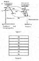
- the organic electroluminescence device of the present invention comprises an anode 02, a hole transport layer 05, a luminescent layer 06, an electron transport layer 07 and a cathode 03, which are successively deposited on a substrate 01 and are laminated.
- the thermally activated and sensitized organic electroluminescence device of the present invention comprises a luminescent layer, wherein the host material of the luminescent layer is a mixture of two materials, wherein one of the two materials is a hole transport material, the other is an electron transport material, and at least one of the two materials is a thermally activated delayed fluorescence material; and the host material is doped by a phosphorescent dye, and the doping concentration of the phosphorescent dye in the host material is ⁇ 15wt%, preferably 2wt%-10wt%, more preferably 2wt%-3wt%.
- the triplet state energy level of the CT excited state of the thermally activated delayed fluorescence material is higher than the triplet state energy level of the n- ⁇ excited state by 0 to 0.3; or, the triplet state energy level of the CT excited state of the thermally activated delayed fluorescence material is higher than the triplet state energy level of the n- ⁇ excited state, wherein the difference is above 1.0eV, and, a difference between the second triplet state energy level of its n- ⁇ excited state and the first singlet state energy level of its CT excited state is-0.1 to 0.1eV.
- one of the host materials of the luminescent layer is a hole transport material
- the other is an electron transport material
- at least one of the two materials is a thermally activated delayed fluorescence material.
- the energy of the triplet state excitons of the host material is transferred to the singlet state by reverse intersystem crossing, and then transferred to the triplet state of the phosphorescence material by long range Forster energy transfer, which improves the energy transfer relation between the host and guest luminophor, to reduce the doping proportion ( ⁇ 15%), save the cost, effectively suppress attenuation, and prolong the life.
- the energy conversion and the luminescence are not in the same material, and thus the performance of the device is better.
- the thermally activated delayed fluorescence material is a material whose triplet state energy level of the CT excited state is higher than the triplet state energy level of the n- ⁇ excited state with a difference between 0-0.3eV; or, the thermally activated delayed fluorescence material is a material whose triplet state energy level of the CT excited state is higher than the triplet state energy level of the n- ⁇ excited state with a difference above 1.0eV and whose difference between the second triplet state energy level of the n- ⁇ excited state and the first singlet state energy level of the CT excited state is -0.1 to 0.1eV.
- the thermally activated delayed fluorescence material of the present invention is a material whose difference between the triplet state of the CT excited state and the triplet state energy level of the n- ⁇ excited state is very small (0-0.3eV), or a material whose above difference is very large ( ⁇ 1.0eV) but whose second triplet state of the n- ⁇ excited state is slightly smaller than or slightly higher than the first singlet state of the CT excited state (with a difference of (0-0.1eV).
- All of the materials that the present invention selects have a donor group and an acceptor group that are separated spatially, thereby resulting in the spatial separation of the HOMO and LUMO energy levels and reducing overlap integral, and thus the difference between the energy level differences between the singlet states and the triplet states of the CT states of the materials is very small. Additionally, the energy level differences between the singlet states and the triplet states of the chosen phenanthroimidazolyl, naphthathiazolyl, benzothiazolyl or anthryl are above 1.0eV, which can meet the requirements on the second material.
- the thermally activated delayed fluorescence material in the present invention is a material that has charge transfer transition, and the thermally activated delayed fluorescence material has both a donor group unit and an acceptor group unit therein, wherein, the donor group unit is a donor group or a group that is formed by linking two or more donor groups; and the acceptor group unit is an acceptor group or a group that is formed by linking two or more acceptor groups.
- the structure of the host material may be donor-connection-acceptor, donor-acceptor-donor, and so on.
- the donor group is selected from indolocarbazolyl; carbazolyl; bicarbazolyl; trianilino; phenoxazinyl; indolocarbazolyl that is substituted by one or more groups of C 1-6 alkyl, methoxy, ethoxy or phenyl; carbazolyl that is substituted by one or more groups of C 1-6 alkyl, methoxy, ethoxy or phenyl; dibenzofuranyl that is substituted by one or more groups of C 1-6 alkyl, methoxy, ethoxy or phenyl; trianilino that is substituted by one or more groups of C 1-6 alkyl, methoxy, ethoxy or phenyl; or phenoxazinyl that is substituted by one or more groups of C 1-6 alkyl, methoxy, ethoxy or phenyl; and the acceptor group is selected from naphthyl; anthryl; phenanthryl
- the linking group is preferably selected from spirofluorenyl; phenyl; biphenyl; spirofluorenyl that is substituted by at least one of C 1-6 alkyl or phenyl; phenyl that is substituted by at least one of C 1-6 alkyl or phenyl; or biphenyl that is substituted by at least one of C 1-6 alkyl or phenyl.
- the donor group is preferably selected from the following structures:
- the acceptor group is preferably selected from the following structures:
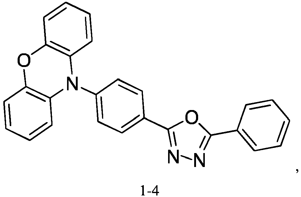
- the thermally activated delayed fluorescence material is selected from the compounds having the following structures: 1-1 ( Chem. Commun., 2012, 48, 9580-9582 ) 1-2 ( Angew. Chem. Int. Ed., 2012, 51, 11311-11315 ) 1-3 ( Chem. Commun. 2012, 48, 11392-11394 ) 1-4 ( J. Mater. Chem. C, 2013, 1, 4599-4604 ) 1-5 ( J. Mater. Chem. C, 2013, 1, 4599-4604 ) 1-6 ( Phys. Chem. Chem.
- the synthesis of the 1-4 can refer to that of the 1-7.
- Substance detection data Mass spectrometry data: ESI-MS m/z: 717 [M + H] + , elementary analysis C 44 H 32 N 2 O 4 S 2 , C: 73.72, H: 4.50, N: 3.91.
- the synthesis of the compound 2-2 can refer to that of 2-1, wherein the method is basically the same as that of the compound 2-1, and the difference is that the 2-1a is replaced by bicarbazole.
- the synthesis of the 2-9 can refer to that of 2-7, wherein the difference is using a different donor group, by replacing phenoxazine with carbazole.
- 4.65g of 2-8a, 3.0g of carbazole, 0.5g of CuI, 0.5g of phenanthroline and 5.2g of potassium carbonate are added into a 100ml round bottom flask, and 60ml of DMF is added.
- the reaction is performed under a nitrogen atmosphere by heating to reflux for 48 hours. Subsequently the reaction liquid is poured into water, and is subject to vacuum filtration under reduced pressure to obtain a solid, The solid is separated by using a chromatographic column to obtain the 2-9, with a yield of 50%.
- the synthesis of the compound 3-4 can refer to the compound 3-3, wherein the steps are basically the same, and the difference is that the acceptor group is benzothiazole substituted by thiophene.
- the synthesis of the compound 3-5 can refer to the compound 3-3, wherein the steps are basically the same, and the difference is that the acceptor group is naphthathiazole substituted by thiophene.
- the two materials that the host material consists of of the present invention may both be a thermally activated delayed fluorescence material, and the energy transfer process is as shown by Fig. 4 : the first TADF host and the second TADF host individually transfer the triplet state energy to the singlet state by reverse intersystem crossing, and then transfer all of the energy to the triplet state of the phosphorescent dye by Forster, thereby reducing the distance between the host and the guest, to utilize the energy of the host with a high efficiency and reduce the consumption of the phosphorescence materials, and effectively solving the problem of roll-off, to improve the stability of the device.
- one of the two materials is a thermally activated delayed fluorescence material (the TADF host), and the other is a regulating host material (regulating host).
- One of them is an electron transport material, and the other is a hole transport material.
- the energy transfer principle is as shown by Fig. 5 : the common triplet state energy of the TADF host and the regulating host is transferred to the singlet state by reverse intersystem crossing, and then transfer all of the energy to the triplet state of the phosphorescent dye by Forster, thereby reducing the distance between the host and the guest, to utilize the energy of the host with a high efficiency and reduce the consumption of the phosphorescence materials, and effectively solving the problem of roll-off, to improve the stability of the device.
- the anode may employ an inorganic material or an organic conductive polymer.
- the inorganic material may generally employ metal oxides such as indium tin oxide (ITO), zinc oxide (ZnO), and indium zinc oxide (IZO) or metals of high work functions such as gold, copper and silver, preferably ITO.
- the organic conductive polymer is preferably one of polythiophene/polyvinyl sodium benzenesulfonate (hereafter referred to as simply PEDOT/PSS) and polyaniline (hereafter referred to as simply PANI).
- the cathode generally employs metals of low work function such as lithium, magnesium, calcium, strontium, aluminum and indium or their alloys with copper, gold or silver, or an electrode layer that is formed by the alternating of a metal and a metal fluoride.
- the cathode is preferably laminated LiF layer and Al layer (the LiF layer is on the outer side).
- the material of the hole transport layer may be selected from lower molecular weight materials of the arylamine type and the branched polymer type, preferably NPB.
- the material of the electron transport layer may employ an organic metal complex (such as Alq 3 , Gaq 3 , BAlq or Ga (Saph-q)) or other materials that are commonly used for electron transport layer, such as aromatic condensed ring type (such as pentacene and perylene) or o-phenanthroline type (such as Bphen and BCP) compounds.
- organic metal complex such as Alq 3 , Gaq 3 , BAlq or Ga (Saph-q)
- other materials that are commonly used for electron transport layer such as aromatic condensed ring type (such as pentacene and perylene) or o-phenanthroline type (such as Bphen and BCP) compounds.
- the organic electroluminescence device of the present invention may also be provided with a hole injection layer 04 (which may be omitted) between the anode and the hole transport layer.
- the material of the hole injection layer may employ, for example, 4,4',4"-tris(3-methylphenylaniline)triphenylamine) doped F4TCNQ or copper phthalocyanine (CuPc), or may be a metal oxide, such as molybdenum oxide and rhenium oxide.
- the thicknesses of the layers may employ the conventional thicknesses of the layers in the art.
- the present invention further provides the preparation method of the organic electroluminescence device, which comprises successively depositing on the substrate 01 the anode 02, the hole transport layer 05, the luminescent layer 06, the electron transport layer 07 and the cathode 03, which are laminated, and packaging.
- the substrate may be glass or a flexible base sheet.
- the flexible base sheet may employ a polyester type or polyimide type compound material or a thin sheet metal.
- the laminating and the packaging may employ any suitable method that is known by a person skilled in the art.
- thermoly activated delayed fluorescence materials that have different doping concentrations of thermally activated delayed fluorescence materials are prepared, and those devices have the structure as shown by Fig. 3 .
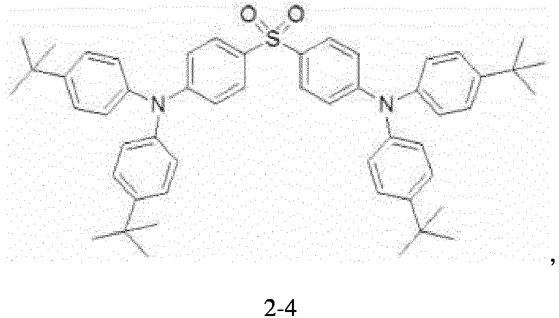
- the host materials of the luminescent layers thermally activated delayed fluorescence materials Host1 (1-9), thermally activated delayed fluorescence materials Host2 (2-4), the phosphorescent dye doping the host materials (Ir(ppy) 3 ).
- the thermally activated delayed fluorescence materials Host2 (2-4) are electron transport materials
- the thermally activated delayed fluorescence materials Host1 (1-9) are hole transport materials
- the structure of the device of this Example is as follows:
- the percentages in the parentheses preceding the phosphorescent dye indicate different doping concentrations, and in this Example and below, the doping concentrations are all in wt%.
- the particular preparation method of the organic electroluminescence device is as follows:
- An organic electroluminescence device is prepared by using the method the same as that of Example 1, and the structure of the device is as follows:
- the host material of the luminescent layer is CBP:BAlq, and the phosphorescent dye is the same as that of Example 1.
- An organic electroluminescence device is prepared by using the method the same as that of Example 1, and the structure of the device is as follows:
- the host materials of the luminescent layers (thermally activated delayed fluorescence materials Host1 (1-9), thermally activated delayed fluorescence materials Host2 (2-4)), and the phosphorescent dye is the same as that of Example 1.
- Example 1 Device Luminescent Layer Composition Luminescence Efficiency (cd/A) Luminance (cd/m 2 ) External Quantum Efficiency (%) Life T90 (hrs)
- Example 1 host material thermoally activated delayed fluorescence material Host 1 (1-9) (39wt%), thermally activated delayed fluorescence material Host 2 (2-4) 44.5 5000 12.5 390 (59wt%):phosphorescent dye (2wt%) host material (thermally activated delayed fluorescence material Host 1 (1-9) (38wt%), thermally activated delayed 46.0 5000 13.3 421 fluorescence material Host 2 (2-4) (59wt%):phosphorescent dye (3wt%) host material (thermally activated delayed fluorescence material Host 1 (1-9) (36%), thermally activated delayed fluorescence material Ho
- thermoly activated delayed fluorescence materials that have different doping concentrations of thermally activated delayed fluorescence materials are prepared, and those devices have the structure as shown by Fig. 3 .
- the host materials of the luminescent layers thermally activated delayed fluorescence materials Host 3 (1-10), regulating host material (CBP), the phosphorescent dye doping the host materials Ir(piq) 3 .
- the thermally activated delayed fluorescence materials Host 3 (1-10) are electron transport materials, and the regulating host material CBP is a hole transport material, wherein their triplet state energy levels are the same): the structure of the device of this Example is as follows:
- the percentages in the parentheses preceding the phosphorescent dye indicate different doping concentrations, and in this Example and below, the doping concentrations are all in wt%.
- An organic electroluminescence device is prepared by using the method the same as that of Example 1, and the structure of the device is as follows:
- the host materials of the luminescent layers (thermally activated delayed fluorescence materials Host 3 (1-10)), regulating host material CBP, and the phosphorescent dye is the same as that of Example 2.
- Example 2 The performances of the organic electroluminescence devices of Example 2 and Comparative Example 3 are as shown by Table 2: Table 2 Device Luminescent Layer Composition Luminescence Efficiency (cd/A) Luminance (cd/m 2 ) External Quantum Efficiency (%) Life T90 (hrs)
- Example 2 host material thermoally 48.6 5000 18.0 457 activated delayed fluorescence material Host 3 (1-10) (59%), regulating host material CBP (39%):phosphorescent dye (2%) host material (thermally activated delayed fluorescence material Host 3 (1-10) (59%), regulating host material CBP 53.5 5000 19.3 490 (38%):phosphorescent dye (3%) host material (thermally activated delayed fluorescence material Host 3 (1-10) (54%), regulating host material CBP 45.1 5000 17.4 423 (36%):phosphorescent dye (10%) host material (thermally activated delayed fluorescence material Host 3 (1-10) (52%), regulating host material CBP 42.5 5000 16.9 410 (34%):phosphorescent
- an organic electroluminescence device is prepared by using the method the same as that of Example 1, and the structure of the luminescence device is as follows:
- OLED3 host material thermally activated delayed fluorescence material 1-1, regulating host material niBr:phosphorescent dye 45.1 5000 13.4 385
- OLED4 host material thermally activated delayed fluorescence material 1-10, regulating host material CBP:phosphorescent dye 57.2 5000 17.6
- OLED5 host material thermally activated delayed fluorescence material 3-10, regulating host material TCTA:phosphorescent dye 51.0 5000 15.7 497
- OLED6 host material thermalally activated delayed fluorescence material 2-5, regulating host material mCP:phosphorescent dye:phosphorescent dye 46.2 5000 14.2 387
- OLED7 host material thermalally activated delayed fluorescence material 1-1, thermally activated delayed fluorescence material 3-1):phosphorescent dye 54.6 5000 16.
Landscapes
- Chemical & Material Sciences (AREA)
- Physics & Mathematics (AREA)
- Engineering & Computer Science (AREA)
- Materials Engineering (AREA)
- Spectroscopy & Molecular Physics (AREA)
- Optics & Photonics (AREA)
- Organic Chemistry (AREA)
- Electroluminescent Light Sources (AREA)
Abstract
Description
- The present invention relates to the field of organic electroluminescence devices, and particularly to a thermally activated and sensitized phosphorescence organic electroluminescence device.
- Presently, in the prior art, the luminescent layers of organic electroluminescence devices are generally formed by a host material doped by a dye. The conventional double host luminescent layers are formed by two hosts doped by a dye (fluorescence or phosphorescence). The host materials of such double host luminescent layers do not have thermally delayed fluorescence effect, and the dye does not have thermally delayed fluorescence characteristics either.
- In the conditions of electric excitation, organic electroluminescence devices generate 25% of singlet state excitons and 75% of triplet state excitons. The conventional fluorescence materials can only utilize the 25% of the singlet state excitons due to spin forbidding, so the external quantum efficiency is limited to merely below 5%. Nearly all of the triplet state excitons can only be lost in the form of heat. In order to improve the efficiency of organic electroluminescence devices, the triplet state excitons must be sufficiently utilized.
- In order to utilize the triplet state excitons, researchers have proposed many methods. What is the most significant is the utilization of phosphorescence materials. Because heavy atoms are introduced into phosphorescence materials, which results in spin-orbit coupling effect, the 75% of triplet state excitons can be sufficiently utilized, thereby achieving 100% of internal quantum efficiency. However, because phosphorescence materials use rare heavy metals, the raw materials are expensive, which is adverse to reduce the product cost. If fluorescence devices can well utilize the triplet state excitons, the problem will be solved satisfactorily. Researchers proposed generating the singlet state in fluorescence devices by using triplet state quenching to improve the efficiency of the fluorescence devices, but the maximum external quantum efficiency that the method can theoretically reach is merely 62.5%, which is far below that of phosphorescence materials. Therefore, to seek a new technique to sufficiently utilize the triplet state energy level of fluorescence materials to improve the luminescence efficiency is highly necessary.
- Adachi et, al. of Kyushu University proposed a new approach to achieve high efficiency fluorescence OLED: thermally activated delayed fluorescence (TADF) materials. The energy gap between singlet state and triplet state (ΔEST) of this type of materials is very small, and the triplet state excitons, which cannot emit light, can be upconverted to singlet state excitons, which can emit light, under the effect of environmental heat. However, when this type of materials directly serve as the luminescent layer, the devices have a long way to go before practical utilization, with efficiency not high enough, short life, and severe roll-off.
- The thermally activated and sensitized luminescence mechanism utilizes a thermally activated delayed fluorescence material as the host and a phosphorescence material as the dye, and can achieve devices of high efficiency, low voltage and long life. That is because in the conventional thermally delayed fluorescence, the energy conversion and the luminescence are within the same single material, while regarding the thermally activated and sensitized devices, the energy conversion and the luminescence are conducted by different materials. That can ensure the sufficient utilization of the triplet state energy, lift the efficiency, reduce the problem of roll-off under high luminance, and prolong the device life.
- As shown by
Fig. 1 , after electrons and holes undergo langevin recombination in an organic molecule, due to the difference in the electron spin symmetry modes, two excited state forms, a single excited state and a triplet excited state, are generated. In the host and guest luminophor system of phosphorescence devices, there are two luminescence mechanisms, energy transfer and trap-assisted mode. The energy transfer comprises long range Forster transfer mode and short range Dexter transfer mode. The trap-assisted mode is by the electrons and the holes directly recombining on the guest luminophor into excitons and in turn exciting the guest luminophor to emit light. In the conventional phosphorescence doping systems, the energy transfer from the triplet state of the host to the triplet state of the guest can only be via the short range Dexter energy transfer, and in order to reduce the distance between the host and the guest and promote the complete transfer of energy, a high doping concentration of the phosphorescence is required (15-20wt%). That will result in high cost, and will cause the degrading of the device efficiency. - The organic electroluminescence devices of the prior art are formed by a host material doped by a dye, which has high cost, and will cause the degrading of the device efficiency.
- The present invention discloses a thermally activated and sensitized phosphorescence organic electroluminescence device, comprising a luminescent layer, wherein the host material of the luminescent layer consists of two materials, wherein one of the two materials is a hole transport material, the other is an electron transport material, and at least one of the two materials is a thermally activated delayed fluorescence material; and the host material is doped by a phosphorescent dye, and a proportion of the phosphorescent dye in the luminescent layer is <15wt%, and
the triplet state energy level of the CT excited state of the thermally activated delayed fluorescence material is higher than the triplet state energy level of the n-π excited state by 0 to 0.3; or, the triplet state energy level of the CT excited state of the thermally activated delayed fluorescence material is higher than the triplet state energy level of the n-π excited state, wherein the difference is above 1.0eV, and, a difference between the second triplet state energy level of its n-π excited state and the first singlet state energy level of its CT excited state is-0.1 to 0.1eV. - Preferably, the proportion of the phosphorescent dye in the luminescent layer is 2wt%-10wt%, more preferably 2wt%-3wt%.
- Preferably, the thermally activated delayed fluorescence material is a material that has charge transfer transition, and the thermally activated delayed fluorescence material has both a donor group unit and an acceptor group unit therein,
the donor group unit is a donor group or a group that is formed by linking two or more donor groups;
the acceptor group unit is an acceptor group or a group that is formed by linking two or more acceptor groups;
the donor group is selected from indolocarbazolyl; carbazolyl; bicarbazolyl; trianilino; phenoxazinyl; indolocarbazolyl that is substituted by one or more groups of C1-6 alkyl, methoxy, ethoxy or phenyl; carbazolyl that is substituted by one or more groups of C1-6 alkyl, methoxy, ethoxy or phenyl; bicarbazolyl that is substituted by one or more groups of C1-6 alkyl, methoxy, ethoxy or phenyl; trianilino that is substituted by one or more groups of C1-6 alkyl, methoxy, ethoxy or phenyl; or phenoxazinyl that is substituted by one or more groups of C1-6 alkyl, methoxy, ethoxy or phenyl; and
the acceptor group is selected from naphthyl; anthryl; phenanthryl; pyrenyl; triazinyl; benzimidazolyl; cyano; pyridinyl; sulfonyl; phenanthroimidazolyl; naphthathiazolyl; benzothiazolyl; oxadiazolyl; naphthyl that is substituted by one or more groups of C1-6 alkyl, methoxy, ethoxy, phenyl or pyridinyl; anthryl that is substituted by one or more groups of C1-6 alkyl, methoxy, ethoxy, phenyl or pyridinyl, phenanthryl that is substituted by one or more groups of C1-6 alkyl, methoxy, ethoxy, phenyl or pyridinyl; pyrenyl that is substituted by one or more groups of C1-6 alkyl, methoxy, ethoxy, phenyl or pyridinyl; triazinyl that is substituted by one or more groups of C1-6 alkyl, methoxy, ethoxy, phenyl or pyridinyl; benzimidazolyl that is substituted by one or more groups of C1-6 alkyl, methoxy, ethoxy, phenyl or pyridinyl; pyridinyl that is substituted by one or more groups of C1-6 alkyl, methoxy, ethoxy, phenyl or pyridinyl; sulfonyl that is substituted by one or more groups of C1-6 alkyl, methoxy, ethoxy, phenyl or pyridinyl; phenanthroimidazolyl that is substituted by one or more groups of C1-6 alkyl, methoxy, ethoxy, phenyl or pyridinyl; naphthathiazolyl that is substituted by one or more groups of C1-6 alkyl, methoxy, ethoxy, phenyl or pyridinyl; benzothiazolyl that is substituted by one or more groups of C1-6 alkyl, methoxy, ethoxy, phenyl or pyridinyl; and oxadiazolyl that is substituted by one or more groups of C1-6 alkyl, methoxy, ethoxy, phenyl or pyridinyl;
wherein, one or more of the donor group unit and one or more of the acceptor group unit directly link to form the thermally activated delayed fluorescence material; or, one or more of the donor group unit and one or more of the acceptor group unit individually link to a linking group to form the thermally activated delayed fluorescence material, wherein the linking group is a group that has a steric hindrance. - Preferably, one or two of the donor group units and one or two of the acceptor group units individually link to the linking group to form the thermally activated delayed fluorescence material, or one or two of the acceptor group units and one or two of the donor group units directly link to form the thermally activated delayed fluorescence material.
- Preferably, the linking group is selected from spirofluorenyl, phenyl, biphenyl, spirofluorenyl that is substituted by at least one of C1-6 alkyl or phenyl, phenyl that is substituted by at least one of C1-6 alkyl or phenyl, and biphenyl that is substituted by at least one of C1-6 alkyl or phenyl.
- Preferably, the donor group is selected from the following groups:




- Preferably, the acceptor group is selected from the following groups:


- Preferably, the thermally activated delayed fluorescence material is a compound that has the following structures:






- As an embodiment, both of the two materials that the host material consists of are thermally activated delayed fluorescence materials.
- Preferably, one of the two materials that the host material consists of is a thermally activated delayed fluorescence material, and the other is a regulating host material, wherein a triplet state energy level of the thermally activated delayed fluorescence material and a triplet state energy level of the regulating host material in the host material are equal.
- The advantages of the present invention are:
- In the thermally activated and sensitized phosphorescence device of the present invention, one of the host materials of the luminescent layer is a hole transport material, the other is an electron transport material, and at least one of the two materials is a thermally activated delayed fluorescence material. In this manner, the triplet state excitons are transferred to the singlet state, which is conducted mainly by long range Forster energy transfer, to reduce the doping proportion (<3%), save the cost, effectively suppress attenuation, and prolong the life. Additionally, the energy conversion and the luminescence are not in the same material, and thus the performance of the device is better.
-
-
Fig. 1 is the schematic diagram of the energy transfer of a conventional OLED luminescent layer phosphorescence system. -
Fig. 2 is the schematic diagram of the structure of the organic electroluminescence device of the present invention. -
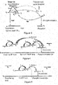
Fig. 3 is the schematic diagram of the energy transfer of the OLED luminescent layer thermally activated and sensitized phosphorescence system of the present invention. -
Fig. 4 is the schematic diagram of the energy transfer of the OLED luminescent layer of the present invention whose host materials are two TADF materials. -
Fig. 5 is the schematic diagram of the energy transfer of the OLED luminescent layer of the present invention whose host materials are a TADF material and a regulating host material. - The present invention will be further illustrated below by referring to the drawings and the special examples, to enable a person skilled in the art to better understand and implement the present invention, but the examples are not taken as limiting the present invention.
- As shown by
Fig. 2 , the organic electroluminescence device of the present invention comprises ananode 02, ahole transport layer 05, aluminescent layer 06, anelectron transport layer 07 and acathode 03, which are successively deposited on asubstrate 01 and are laminated. - The thermally activated and sensitized organic electroluminescence device of the present invention comprises a luminescent layer, wherein the host material of the luminescent layer is a mixture of two materials, wherein one of the two materials is a hole transport material, the other is an electron transport material, and at least one of the two materials is a thermally activated delayed fluorescence material; and the host material is doped by a phosphorescent dye, and the doping concentration of the phosphorescent dye in the host material is <15wt%, preferably 2wt%-10wt%, more preferably 2wt%-3wt%.
- The triplet state energy level of the CT excited state of the thermally activated delayed fluorescence material is higher than the triplet state energy level of the n-π excited state by 0 to 0.3; or, the triplet state energy level of the CT excited state of the thermally activated delayed fluorescence material is higher than the triplet state energy level of the n-π excited state, wherein the difference is above 1.0eV, and, a difference between the second triplet state energy level of its n-π excited state and the first singlet state energy level of its CT excited state is-0.1 to 0.1eV.
- As shown by
Fig. 3 , in the thermally activated and sensitized phosphorescence device of the present invention, one of the host materials of the luminescent layer is a hole transport material, the other is an electron transport material, and at least one of the two materials is a thermally activated delayed fluorescence material. In this manner, the energy of the triplet state excitons of the host material is transferred to the singlet state by reverse intersystem crossing, and then transferred to the triplet state of the phosphorescence material by long range Forster energy transfer, which improves the energy transfer relation between the host and guest luminophor, to reduce the doping proportion (<15%), save the cost, effectively suppress attenuation, and prolong the life. Additionally, the energy conversion and the luminescence are not in the same material, and thus the performance of the device is better. - In the present invention, preferably, the thermally activated delayed fluorescence material is a material whose triplet state energy level of the CT excited state is higher than the triplet state energy level of the n-π excited state with a difference between 0-0.3eV; or, the thermally activated delayed fluorescence material is a material whose triplet state energy level of the CT excited state is higher than the triplet state energy level of the n-π excited state with a difference above 1.0eV and whose difference between the second triplet state energy level of the n-π excited state and the first singlet state energy level of the CT excited state is -0.1 to 0.1eV.
- The thermally activated delayed fluorescence material of the present invention is a material whose difference between the triplet state of the CT excited state and the triplet state energy level of the n-π excited state is very small (0-0.3eV), or a material whose above difference is very large (≥ 1.0eV) but whose second triplet state of the n-π excited state is slightly smaller than or slightly higher than the first singlet state of the CT excited state (with a difference of (0-0.1eV). All of the materials that the present invention selects have a donor group and an acceptor group that are separated spatially, thereby resulting in the spatial separation of the HOMO and LUMO energy levels and reducing overlap integral, and thus the difference between the energy level differences between the singlet states and the triplet states of the CT states of the materials is very small. Additionally, the energy level differences between the singlet states and the triplet states of the chosen phenanthroimidazolyl, naphthathiazolyl, benzothiazolyl or anthryl are above 1.0eV, which can meet the requirements on the second material.
- The thermally activated delayed fluorescence material in the present invention is a material that has charge transfer transition, and the thermally activated delayed fluorescence material has both a donor group unit and an acceptor group unit therein, wherein, the donor group unit is a donor group or a group that is formed by linking two or more donor groups; and the acceptor group unit is an acceptor group or a group that is formed by linking two or more acceptor groups. Specially, the structure of the host material may be donor-connection-acceptor, donor-acceptor-donor, and so on.
- The donor group is selected from indolocarbazolyl; carbazolyl; bicarbazolyl; trianilino; phenoxazinyl; indolocarbazolyl that is substituted by one or more groups of C1-6 alkyl, methoxy, ethoxy or phenyl; carbazolyl that is substituted by one or more groups of C1-6 alkyl, methoxy, ethoxy or phenyl; dibenzofuranyl that is substituted by one or more groups of C1-6 alkyl, methoxy, ethoxy or phenyl; trianilino that is substituted by one or more groups of C1-6 alkyl, methoxy, ethoxy or phenyl; or phenoxazinyl that is substituted by one or more groups of C1-6 alkyl, methoxy, ethoxy or phenyl; and
the acceptor group is selected from naphthyl; anthryl; phenanthryl; pyrenyl; triazinyl; benzimidazolyl; cyano; pyridinyl; sulfonyl; phenanthroimidazolyl; naphthathiazolyl; benzothiazolyl; oxadiazolyl; naphthyl that is substituted by one or more groups of C1-6 alkyl, methoxy, ethoxy, phenyl or pyridinyl; anthryl that is substituted by one or more groups of C1-6 alkyl, methoxy, ethoxy, phenyl or pyridinyl; phenanthryl that is substituted by one or more groups of C1-6 alkyl, methoxy, ethoxy, phenyl or pyridinyl; pyrenyl that is substituted by one or more groups of C1-6 alkyl, methoxy, ethoxy, phenyl or pyridinyl; triazinyl that is substituted by one or more groups of C1-6 alkyl, methoxy, ethoxy, phenyl or pyridinyl; benzimidazolyl that is substituted by one or more groups of C1-6 alkyl, methoxy, ethoxy, phenyl or pyridinyl; pyridinyl that is substituted by one or more groups of C1-6 alkyl, methoxy, ethoxy, phenyl or pyridinyl; sulfonyl that is substituted by one or more groups of C1-6 alkyl, methoxy, ethoxy, phenyl or pyridinyl; phenanthroimidazolyl that is substituted by one or more groups of C1-6 alkyl, methoxy, ethoxy, phenyl or pyridinyl; naphthathiazolyl that is substituted by one or more groups of C1-6 alkyl, methoxy, ethoxy, phenyl or pyridinyl; benzothiazolyl that is substituted by one or more groups of C1-6 alkyl, methoxy, ethoxy, phenyl or pyridinyl; or oxadiazolyl that is substituted by one or more groups of C1-6 alkyl, methoxy, ethoxy, phenyl or pyridinyl;
wherein, one or more of the donor group units and one or more of the acceptor group units directly link to form the thermally activated delayed fluorescence material; or, one or more of the donor group units and one or more of the acceptor group units individually link to a linking group to form the thermally activated delayed fluorescence material, wherein the linking group is a group that has a steric hindrance. - The linking group is preferably selected from spirofluorenyl; phenyl; biphenyl; spirofluorenyl that is substituted by at least one of C1-6 alkyl or phenyl; phenyl that is substituted by at least one of C1-6 alkyl or phenyl; or biphenyl that is substituted by at least one of C1-6 alkyl or phenyl.
- The donor group is preferably selected from the following structures:


- The acceptor group is preferably selected from the following structures:


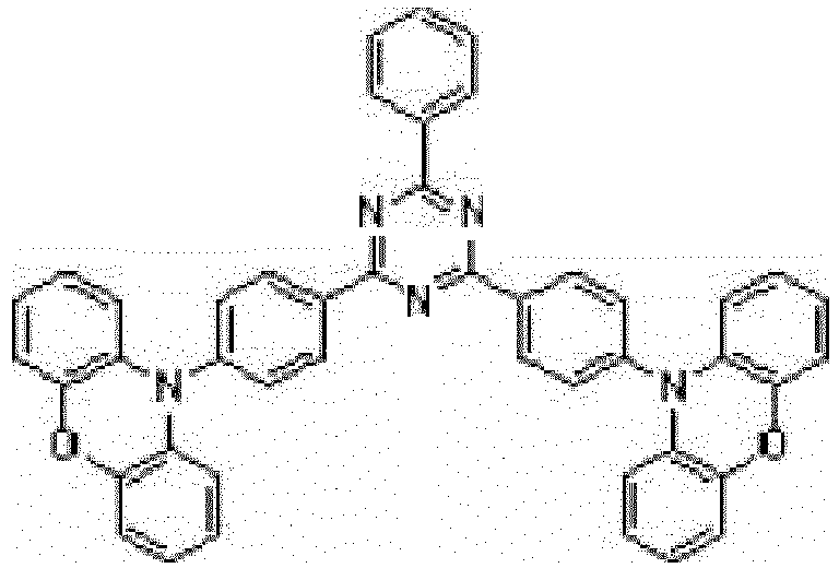
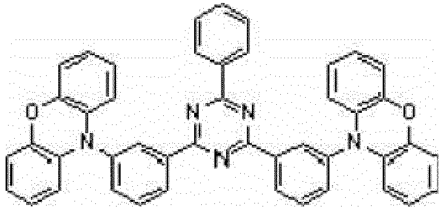
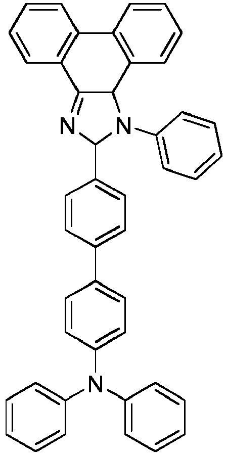
- Particularly, the thermally activated delayed fluorescence material is selected from the compounds having the following structures:
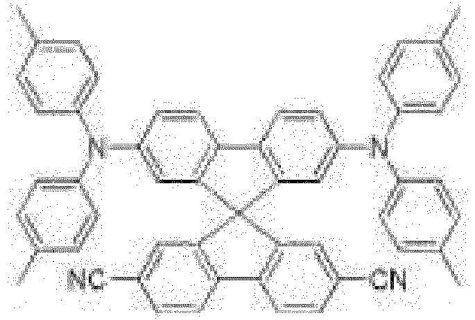
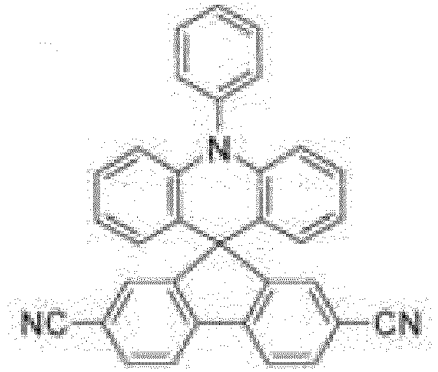


Gaussian 03/TD-DFT)
Gaussian 03/TD-DFT)
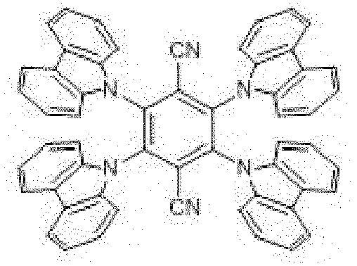


Gaussian 03/TD-DFT)
Gaussian 03/TD-DFT)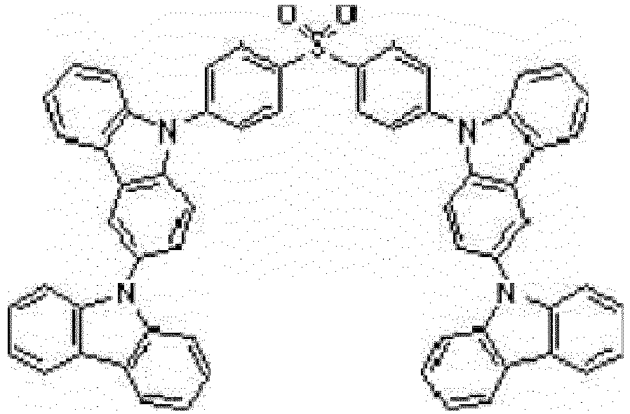
Gaussian 03/TD-DFT)


Gaussian 03/TD-DFT)
Gaussian 03/TD-DFT)
Gaussian 03/TD-DFT)

Gaussian 03/TD-DFT)




Gaussian 03/TD-DFT)
Gaussian 03/TD-DFT)
Gaussian 03/TD-DFT)


- The syntheses of the relative compounds in the present application:
-

- 3.34g of carbazole, 3.22g of 3,6-dibromocarbazole, 0.5g of CuI, 0.5g phenanthroline and 5.2g of potassium carbonate are added into a 100ml round bottom flask, and 60ml of DMF is added. The reaction is performed under a nitrogen atmosphere by heating to reflux for 48 hours. Subsequently the reaction liquid is poured into water, and is subject to vacuum filtration under reduced pressure to obtain a solid. The solid is separated by using a chromatographic column to obtain the 1-7a, with a yield of 30%.
Mass spectrometry data: ESI-MS m/z: 498 [M+H]+, elementary analysis: C36H23N3: C: 86.90, H: 4.66, N: 8.44. - 3.11g of tribromobenzene, 2.48g of p-methylbenzenethiol, 6g of potassium carbonate, and 1g of copper iodide are added into a 100ml round bottom flask, and 50ml of DMF is added. The mixture is heated at 100°C under a nitrogen atmosphere for 24 hours. Subsequently the reaction liquid is poured into water, and is subject to vacuum filtration under reduced pressure to obtain a solid. The solid is separated by using a chromatographic column to obtain the 1-7b, with a yield of 60%.
Mass spectrometry data: ESI-MS m/z: 401 [M+H]+, elementary analysis: C20H17BrS, C: 59.85, H: 4.27. - In an ice water bath, 30ml of the 1-7b is slowly dropped into a dichloromethane solution in 1g of mCPBA, the mixture is maintained in the ice water bath till the addition ends, and subsequently the reaction is performed for 12h. The solid is separated by using a chromatographic column to obtain the 1-7c, with a yield of 99%.
Mass spectrometry data: ESI-MS m/z: 465 [M+H]+, elementary analysis: C20H17BrO4S2, C: 86.90, H: 4.66, N: 8.44. - 4.97g of 1-7a, 4.63g of 1-7b, 0.5g of CuI, 0.5g of phenanthroline and 5.2g of potassium carbonate are added into a 100ml round bottom flask, and 60ml of DMF is added. The reaction is performed under a nitrogen atmosphere by heating to reflux for 48 hours. Subsequently the reaction liquid is poured into water, and is subject to vacuum filtration under reduced pressure to obtain a solid. The solid is separated by using a chromatographic column to obtain the 1-7, with a yield of 60%.
Mass spectrometry data: ESI-MS m/z: 882 [M+H]+, elementary analysis: C56H39N3O4S2, C 76.25, H 4.46, N 4.76. - The synthesis of the 1-4 can refer to that of the 1-7. Substance detection data: Mass spectrometry data: ESI-MS m/z: 717 [M+H]+, elementary analysis C44H32N2O4S2, C: 73.72, H: 4.50, N: 3.91.
-

- 4.52g of 1-8a, 3g of 1-8b and 0.05g of tetrakis(triphenylphosphine)palladium, and 5.4g of potassium carbonate are added into a round bottom flask, and then 30ml of toluene, 20ml of water and 5ml of ethanol are added. The reaction is performed at 85°C for 48h. When the reaction ends, the mixture is extracted by using dichloromethane to obtain an organic layer, and then the organic layer is separated by using a chromatographic column to obtain the 1-8, with a yield of 65%.
Mass spectrometry data: ESI-MS m/z: 640 [M+H]+, elementary analysis: C45H29N5, C: 84.48, H: 4.57, N: 10.95. -
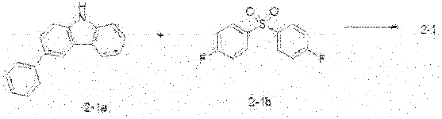
- 2.43g of 2-1a is added into an ultra-dry solution (30ml) of 0.24g of NaH, and is stirred at room temperature for 30 min. Then a DMF solution of 2.54g of 2-1b is dropped into the above solution, heated to 100°C, and stirred for 1 hour. After being cooled, the mixture is poured into water, and the solid is filtered, and separated by using a chromatographic column, to obtain 2-1.
Mass spectrometry data: ESI-MS m/z: 701 [M+H]+, elementary analysis: C48H32N2O2S, C: 82.26, H: 4.60, N: 4.0. - The synthesis of the compound 2-2 can refer to that of 2-1, wherein the method is basically the same as that of the compound 2-1, and the difference is that the 2-1a is replaced by bicarbazole.
Mass spectrometry data: ESI-MS m/z: 879 [M+H]+, elementary analysis: C60H38N4O2S, C: 81.98, H: 4.36, N: 6.37. -

- 2.25g of 2,4-dichloro-6-phenyl triazine, 2g of m-bromophenylboronic acid, 0.05g of tetrakis(triphenylphosphine)palladium, and 5.4g of potassium carbonate are added into a round bottom flask, and then 30ml of toluene, 20ml of water and 5ml of ethanol are added. The reaction is performed at 85°C for 48h. When the reaction ends, the mixture is extracted by using dichloromethane to obtain an organic layer, and then the organic layer is separated by using a chromatographic column to obtain the 2-7a, with a yield of 58%.
Mass spectrometry data: ESI-MS m/z: 466 [M+H]+, elementary analysis: C21H13Br2N3, C: 53.99, H: 2.80, N: 8.99. - 4.65g of 2-7a, 3.66g of phenoxazine, 0.5g of CuI, 0.5g of phenanthroline and 5.2g of potassium carbonate are added into a 100ml round bottom flask, and 60ml of DMF is added. The reaction is performed under a nitrogen atmosphere by heating to reflux for 48 hours. Subsequently the reaction liquid is poured into water, and is subject to vacuum filtration under reduced pressure to obtain a solid, The solid is separated by using a chromatographic column to obtain the 2-7, with a yield of 48%.
Mass spectrometry data: ESI-MS m/z: 672 [M+H]+, elementary analysis: C45H29N5O2, C: 80.46, H: 4.35, N: 4.76. - 2.25g of 2,4-dichloro-6-phenyl triazine, 2g of p-bromophenylboronic acid, 0.05g of tetrakis(triphenylphosphine)palladium, and 5.4g of potassium carbonate are added into a round bottom flask, and then 30ml of toluene, 20ml of water and 5ml of ethanol are added. The reaction is performed at 85°C for 48h. When the reaction ends, the mixture is extracted by using dichloromethane to obtain an organic layer, and then the organic layer is separated by using a chromatographic column to obtain the 2-8a, with a yield of 55%.
Mass spectrometry data: ESI-MS m/z: 466 [M+H]+, elementary analysis: C21H13Br2N3, C: 53.99, H: 2.80, N: 8.99. - 4.65g of 2-8a, 3.66g of phenoxazine, 0.5g of CuI, 0.5g of phenanthroline and 5.2g of potassium carbonate are added into a 100ml round bottom flask, and 60ml of DMF is added. The reaction is performed under a nitrogen atmosphere by heating to reflux for 48 hours. Subsequently the reaction liquid is poured into water, and is subject to vacuum filtration under reduced pressure to obtain a solid, The solid is separated by using a chromatographic column to obtain the 2-8, with a yield of 56%.
Mass spectrometry data: ESI-MS m/z: 640 [M+H]+, elementary analysis: C45H29N5, C: 84.48, H: 4.57, N: 10.95. - The synthesis of the 2-9 can refer to that of 2-7, wherein the difference is using a different donor group, by replacing phenoxazine with carbazole. 4.65g of 2-8a, 3.0g of carbazole, 0.5g of CuI, 0.5g of phenanthroline and 5.2g of potassium carbonate are added into a 100ml round bottom flask, and 60ml of DMF is added. The reaction is performed under a nitrogen atmosphere by heating to reflux for 48 hours. Subsequently the reaction liquid is poured into water, and is subject to vacuum filtration under reduced pressure to obtain a solid, The solid is separated by using a chromatographic column to obtain the 2-9, with a yield of 50%.
Mass spectrometry data: ESI-MS m/z: 640 [M+H]+, elementary analysis: C45H29N5, C: 84.48, H: 4.57, N: 10.95. -

- 3.32g of phenylindolocarbazole, 2.67g 2-chloro-4,6-diphenyl triazine, 0.5g of CuI, 0.5g of phenanthroline and 5.2g of potassium carbonate are added into a 100ml round bottom flask, and 60ml of DMF is added. The reaction is performed under a nitrogen atmosphere by heating to reflux for 48 hours. Subsequently the reaction liquid is poured into water, and is subject to vacuum filtration under reduced pressure to obtain a solid. The solid is separated by using a chromatographic column to obtain the 2-7, with a yield of 48%.
Mass spectrometry data: ESI-MS m/z: 564 [M+H]+, elementary analysis: C39H25N5, C: 83.10, H: 4.47, N: 12.43. -

- 3ml of pyridine is added into a mixed solution of o-phenylene diamine (0.6 g) and thionyl chloride (5ml), stirred at 60°C for 10 hours, extracted by using dichloromethane, and then washed by using a large amount of water to obtain a solid.
Mass spectrometry data: ESI-MS m/z: 205. - 2.25g of 3-3a, 2g of phenylboronic acid, 0.05g of tetrakis(triphenylphosphine)palladium, and 5.4g of potassium carbonate are added into a round bottom flask, and then 30ml of toluene, 20ml of water and 5ml of ethanol are added. The reaction is performed at 85°C for 48h. When the reaction ends, the mixture is extracted by using dichloromethane to obtain an organic layer, and then the organic layer is separated by using a chromatographic column to obtain the 3-3a, with a yield of 58%.
Mass spectrometry data: ESI-MS m/z: 246 [M+H]+. - 2.46g of 3-3b, 2.39g of 4-boric acid triphenylamine, 0.05g of tetrakis(triphenylphosphine)palladium, and 5.4g of potassium carbonate are added into a round bottom flask, and then 30ml of toluene, 20ml of water and 5ml of ethanol are added. The reaction is performed at 85°C for 48h, When the reaction ends, the mixture is extracted by using dichloromethane to obtain an organic layer, and then the organic layer is separated by using a chromatographic column to obtain the 3-3, with a yield of 58%.
Mass spectrometry data: ESI-MS m/z: 456 [M+H]+, elementary analysis: C30H21N3S, C: 79.09, H: 4.65, N: 9.22. - The synthesis of the compound 3-4 can refer to the compound 3-3, wherein the steps are basically the same, and the difference is that the acceptor group is benzothiazole substituted by thiophene.
Mass spectrometry data: ESI-MS m/z: 462 [M+H]+, elementary analysis: C28H19N3S2: C: 72.86, H: 4.15, N: 9.10. - The synthesis of the compound 3-5 can refer to the compound 3-3, wherein the steps are basically the same, and the difference is that the acceptor group is naphthathiazole substituted by thiophene.
Mass spectrometry data: ESI-MS m/z: 512 [M+H]+, elementary analysis: C32H21N3S2: C: 75.12, H: 4.15, N: 8.21. - The two materials that the host material consists of of the present invention may both be a thermally activated delayed fluorescence material, and the energy transfer process is as shown by
Fig. 4 : the first TADF host and the second TADF host individually transfer the triplet state energy to the singlet state by reverse intersystem crossing, and then transfer all of the energy to the triplet state of the phosphorescent dye by Forster, thereby reducing the distance between the host and the guest, to utilize the energy of the host with a high efficiency and reduce the consumption of the phosphorescence materials, and effectively solving the problem of roll-off, to improve the stability of the device. - Alternatively, one of the two materials is a thermally activated delayed fluorescence material (the TADF host), and the other is a regulating host material (regulating host). One of them is an electron transport material, and the other is a hole transport material. The energy transfer principle is as shown by
Fig. 5 : the common triplet state energy of the TADF host and the regulating host is transferred to the singlet state by reverse intersystem crossing, and then transfer all of the energy to the triplet state of the phosphorescent dye by Forster, thereby reducing the distance between the host and the guest, to utilize the energy of the host with a high efficiency and reduce the consumption of the phosphorescence materials, and effectively solving the problem of roll-off, to improve the stability of the device. - The embodiments of the organic luminescence display device of the present invention: The anode may employ an inorganic material or an organic conductive polymer. The inorganic material may generally employ metal oxides such as indium tin oxide (ITO), zinc oxide (ZnO), and indium zinc oxide (IZO) or metals of high work functions such as gold, copper and silver, preferably ITO. The organic conductive polymer is preferably one of polythiophene/polyvinyl sodium benzenesulfonate (hereafter referred to as simply PEDOT/PSS) and polyaniline (hereafter referred to as simply PANI).
- The cathode generally employs metals of low work function such as lithium, magnesium, calcium, strontium, aluminum and indium or their alloys with copper, gold or silver, or an electrode layer that is formed by the alternating of a metal and a metal fluoride. In the present invention the cathode is preferably laminated LiF layer and Al layer (the LiF layer is on the outer side).
- The material of the hole transport layer may be selected from lower molecular weight materials of the arylamine type and the branched polymer type, preferably NPB.
- The material of the electron transport layer may employ an organic metal complex (such as Alq3, Gaq3, BAlq or Ga (Saph-q)) or other materials that are commonly used for electron transport layer, such as aromatic condensed ring type (such as pentacene and perylene) or o-phenanthroline type (such as Bphen and BCP) compounds.
- The organic electroluminescence device of the present invention may also be provided with a hole injection layer 04 (which may be omitted) between the anode and the hole transport layer. The material of the hole injection layer may employ, for example, 4,4',4"-tris(3-methylphenylaniline)triphenylamine) doped F4TCNQ or copper phthalocyanine (CuPc), or may be a metal oxide, such as molybdenum oxide and rhenium oxide.
- The thicknesses of the layers may employ the conventional thicknesses of the layers in the art.
- The present invention further provides the preparation method of the organic electroluminescence device, which comprises successively depositing on the
substrate 01 theanode 02, thehole transport layer 05, theluminescent layer 06, theelectron transport layer 07 and thecathode 03, which are laminated, and packaging. - The substrate may be glass or a flexible base sheet. The flexible base sheet may employ a polyester type or polyimide type compound material or a thin sheet metal. The laminating and the packaging may employ any suitable method that is known by a person skilled in the art.
- For convenience, the abbreviations and full names of some organic materials that are involved in the description are listed as follows:
Abbreviation Full name Structural formula Alq3 tris(8-hydroxylquinoline)a luminum 
BAlq di(2-methyl-8-quinolinyl)-4-phenylphenolaluminum (III) 
BCP 2,9-dimethyl-4,7-diphenyl-1,10-o-phenanthroline 
Bphen 4,7-diphenyl-1,10-o-phena nthroline 
C545T 10-(2-benzothiazole)-1,1,7 ,7,-tetramethyl-2,3,6,7-tetr ahydro-1H,5H,11H-benzo[ 1]pyran[6,7,8-ij]quinolizin e 
CBP 4,4'-N,N'-dicarbazole-biph enyl 
CPF 9,9-di(4-dicarbazole-phen yl)fluorine 
m-MTDATA 4,4',4"-tris(3-methylpheny laniline)triphenylamine 
NPB N,N'-di-(1-naphthyl)-N,N' -diphenyl-1,1'-biphenyl-4, 4'-diamine 
PBD 2-(4-tertbutylphenyl)-5-(4-biphenyl)-1,3,4-oxadiazol 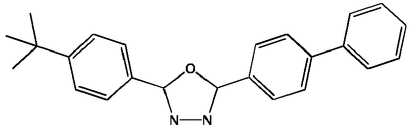
Pentacene pentacene 
TPD N,N'-diphenyl-N,N'-bis(m-methylphenyl)-1,1'-biphen yl-4,4'-diamine 
perylene perylene 
DCJTB 4-4-dicyanomethylene-2-t ertbutyl-6-(1,1,7,7-tetrame thyl-julolidine-9-ethenyl)-4H-pyran 
DCM 4-dicyanomethylene-2-met hyl-6-(p-dimethylaminosty renyl)-4H-pyran 
Rubrene 5,6,11,12-tetraphenyltetrac ene 
DCM-1 4-(dimercaptomethylene)-2-methyl-6-(p-dimethylam inostyrenyl)-4H-pyrane 
DMQA N,N'-dimethylquinacridon e 
F4TCNQ 2,3,5,6-tetrafluoro-7,7',8,8 '-tetracyanodimethyl-p-be nzoquinone 
niBr N-2,6-dibromophenyl-1,8-naphthalimide 
TCTA 4,4',4"-tris(carbazol-9-yl)t rianiline 
mCP 1,3-dicarbazol-9-ylbenzen e 
Ir(ppy)3 tris(2-phenylpyridine) iridium(III) 
Ir(piq)3 tris(1-phenyl-isoquinoline) iridium(III) 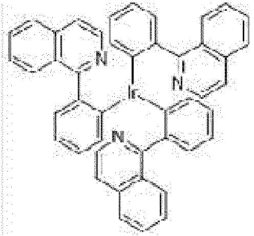
- The present invention is further illustrated below by the Examples.
- In this Example luminescence devices that have different doping concentrations of thermally activated delayed fluorescence materials are prepared, and those devices have the structure as shown by
Fig. 3 . The host materials of the luminescent layers (thermally activated delayed fluorescence materials Host1 (1-9), thermally activated delayed fluorescence materials Host2 (2-4), the phosphorescent dye doping the host materials (Ir(ppy)3). The thermally activated delayed fluorescence materials Host2 (2-4) are electron transport materials, and the thermally activated delayed fluorescence materials Host1 (1-9) are hole transport materials): - The structure of the device of this Example is as follows:
- ITO (150nm)/NPB (40nm)/host material: (2%, 3%, 10%, 14%) phosphorescent dye (30nm)/Alq3 (20nm)/LiF (0.5nm)/Al (150nm)
- In that, the percentages in the parentheses preceding the phosphorescent dye indicate different doping concentrations, and in this Example and below, the doping concentrations are all in wt%.
- The particular preparation method of the organic electroluminescence device is as follows:
- Firstly, washing a glass substrate by using a detergent and deionized water, drying it in an infrared lamp, and sputtering a layer of anode material on the glass, with the film thickness of 150nm;
- then, placing the glass substrate having an anode into a vacuum cavity, vacuumizing to 1×10⁻⁴ Pa, and continually coating by vaporization NPB on the anode layer film as the hole transport layer, with the film forming speed of 0.1nm/s and the vaporization coating film thickness of 40nm;
- coating by vaporization the luminescent layer on the hole transport layer, by the approach of double source co-vaporization, by adjusting the film forming speed by using a film thickness monitor according to the mass percentage between the host material and the phosphorescent dye, with the vaporization coating film thickness of 30nm;
- continually coating by vaporization a layer of Alq3 material on the luminescent layer as the electron transport layer, with the vaporization coating speed of 0.1nm/s and the total vaporization coating film thickness of 20nm; and
- finally coating by vaporization successively a LiF layer and an Al layer on the luminescent layer as the cathode layer of the device, wherein the vaporization coating speed of the LiF layer is 0.01-0.02nm/s and the thickness is 0.5nm, and the vaporization coating speed of the Al layer is 1.0nm/s and the thickness is 150nm.
- An organic electroluminescence device is prepared by using the method the same as that of Example 1, and the structure of the device is as follows:
- ITO (150nm)/NPB (40nm)/host material: (15%) phosphorescent dye (30nm)/Alq3 (20nm)/LiF (0.5nm)/Al (150nm)
- The host material of the luminescent layer is CBP:BAlq, and the phosphorescent dye is the same as that of Example 1.
- An organic electroluminescence device is prepared by using the method the same as that of Example 1, and the structure of the device is as follows:
- ITO (150nm)/NPB (40nm)/host material: (15%, 20%) phosphorescent dye (30nm)/Alq3 (20nm)/LiF (0.5nm)/Al (150nm)
- The host materials of the luminescent layers (thermally activated delayed fluorescence materials Host1 (1-9), thermally activated delayed fluorescence materials Host2 (2-4)), and the phosphorescent dye is the same as that of Example 1.
- The performances of the organic electroluminescence devices of Example 1 and Comparative Example 1 are presented in Table 1, and the percentages of the luminescent layer compositions in the table indicate the mass percentages of the components in the luminescent layers:
Table 1 Device Luminescent Layer Composition Luminescence Efficiency (cd/A) Luminance (cd/m2) External Quantum Efficiency (%) Life T90 (hrs) Example 1 host material (thermally activated delayed fluorescence material Host 1 (1-9) (39wt%), thermally activated delayed fluorescence material Host 2 (2-4) 44.5 5000 12.5 390 (59wt%):phosphorescent dye (2wt%) host material (thermally activated delayed fluorescence material Host 1 (1-9) (38wt%), thermally activated delayed 46.0 5000 13.3 421 fluorescence material Host 2 (2-4) (59wt%):phosphorescent dye (3wt%) host material (thermally activated delayed fluorescence material Host 1 (1-9) (36%), thermally activated delayed fluorescence material Host 2 38.4 5000 11.4 378 (2-4) (54%):phosphorescent dye (10 %) host material (thermally activated delayed fluorescence material Host 1 (1-9) (34%), thermally activated delayed fluorescence material Host 2 35.1 5000 10.1 370 (2-4) (52%)):phosphorescent dye (14 %) Comparative Example 1 host material (CBP (34%):BAlq 28.0 5000 8.0 289 (51%)):phosphorescent dye (15 %) Comparative Example 2 host material (thermally activated delayed fluorescence material Host 1 (1-9) (34%), thermally activated delayed fluorescence material Host 2 32.7 5000 9.7 345 (2-4) (51%):phosphorescent dye (15 %) host material (thermally activated delayed fluorescence material Host 1 (1-9) (32%), thermally activated delayed fluorescence material Host 2 29 5000 6.4 296 (2-4) (48%):phosphorescent dye (20 %) - It can be seen from Table 1 that, when the host material employs the mixture of an electron transport material and a hole transport material, and they both employ a TADF material, the luminescence efficiencies of the double thermally activated delayed fluorescence host materials are obviously increased compared with the efficiency of the single host material, and the lives are also obviously increased compared with the lives of the traditional double host devices.
- In addition, when the doping concentrations of the phosphorescent dyes are less than 15%, their luminescence efficiencies are all higher than the efficiencies when the doping concentrations are > 15%, the lives are also increased, and the big amount of the consumption of the expensive phosphorescent dye is eliminated.
- In this Example luminescence devices that have different doping concentrations of thermally activated delayed fluorescence materials are prepared, and those devices have the structure as shown by
Fig. 3 . The host materials of the luminescent layers (thermally activated delayed fluorescence materials Host 3 (1-10), regulating host material (CBP), the phosphorescent dye doping the host materials Ir(piq)3. The thermally activated delayed fluorescence materials Host 3 (1-10) are electron transport materials, and the regulating host material CBP is a hole transport material, wherein their triplet state energy levels are the same): the structure of the device of this Example is as follows: - ITO (150nm)/NPB (40nm)/host material: (2%, 3%, 10%, 14%) phosphorescent dye (30nm)/Alq3 (20nm)/LiF (0.5nm)/Al (150nm)
- In that, the percentages in the parentheses preceding the phosphorescent dye indicate different doping concentrations, and in this Example and below, the doping concentrations are all in wt%.
- An organic electroluminescence device is prepared by using the method the same as that of Example 1, and the structure of the device is as follows:
- ITO (150nm)/NPB (40nm)/host material: (15%, 20%) phosphorescent dye (30nm)/Alq3 (20nm)/LiF (0.5nm)/Al (150nm)
- The host materials of the luminescent layers (thermally activated delayed fluorescence materials Host 3 (1-10)), regulating host material CBP, and the phosphorescent dye is the same as that of Example 2.
- The performances of the organic electroluminescence devices of Example 2 and Comparative Example 3 are as shown by Table 2:
Table 2 Device Luminescent Layer Composition Luminescence Efficiency (cd/A) Luminance (cd/m2) External Quantum Efficiency (%) Life T90 (hrs) Example 2 host material (thermally 48.6 5000 18.0 457 activated delayed fluorescence material Host 3 (1-10) (59%), regulating host material CBP (39%):phosphorescent dye (2%) host material (thermally activated delayed fluorescence material Host 3 (1-10) (59%), regulating host material CBP 53.5 5000 19.3 490 (38%):phosphorescent dye (3%) host material (thermally activated delayed fluorescence material Host 3 (1-10) (54%), regulating host material CBP 45.1 5000 17.4 423 (36%):phosphorescent dye (10%) host material (thermally activated delayed fluorescence material Host 3 (1-10) (52%), regulating host material CBP 42.5 5000 16.9 410 (34%):phosphorescent dye (14%) Comparative Example 3 host material (thermally activated delayed fluorescence material Host 3 (1-10) (51%), regulating host material CBP 41.7 5000 16.8 407 (34%):phosphorescent dye (15%) host material (thermally activated delayed fluorescence material Host 3 (1-10) (48%), regulating host material CBP 39.2 5000 13.5 389 (32%):phosphorescent dye (20%) - It can be seen from Table 2 that, when the doping concentrations of the phosphorescent dyes are less than 15%, their luminescence efficiencies are all higher than the efficiencies when the doping concentrations are > 15%, the lives are also increased, and the big amount of the consumption of the expensive phosphorescent dye is eliminated.
- In order to test the influence of the host materials of the present invention on the performance of the organic electroluminescence device, in this Example an organic electroluminescence device is prepared by using the method the same as that of Example 1, and the structure of the luminescence device is as follows:
- ITO (150nm)/NPB (40nm)/host material (the mass ratio of the two host materials is 1:1): 3% phosphorescent dye (Ir(ppy)3) (30nm)/Bphen (20nm)/LiF (0.5nm)/Al (150nm).
- The performance of the organic electroluminescence device is presented in Table 3:
Table 3 Device Luminescent Layer Structure Luminescence Efficiency (cd/A) Luminance (cd/m2) External Quantum Efficiency (%) Life T90 (hrs) OLED3 host material (thermally activated delayed fluorescence material 1-1, regulating host material niBr):phosphorescent dye 45.1 5000 13.4 385 OLED4 host material (thermally activated delayed fluorescence material 1-10, regulating host material CBP):phosphorescent dye 57.2 5000 17.6 510 OLED5 host material (thermally activated delayed fluorescence material 3-10, regulating host material TCTA):phosphorescent dye 51.0 5000 15.7 497 OLED6 host material (thermally activated delayed fluorescence material 2-5, regulating host material mCP:phosphorescent dye:phosphorescent dye 46.2 5000 14.2 387 OLED7 host material (thermally activated delayed fluorescence material 1-1, thermally activated delayed fluorescence material 3-1):phosphorescent dye 54.6 5000 16.8 459 OLED8 host material (thermally activated delayed fluorescence material 1-2, thermally activated delayed fluorescence material 2-4):phosphorescent dye 63.4 5000 19.5 513 OLED9 host material (thermally activated delayed fluorescence material 1-9, thermally activated delayed fluorescence material 3-4):phosphorescent 48.7 5000 16.4 335 dye OLED10 host material (thermally activated delayed fluorescence material 1-14, thermally activated delayed fluorescence material 3-7):phosphorescent dye 38.9 5000 14.7 412 - The above examples are merely preferred examples that are presented to fully illustrate the present invention, and the protection scope of the present invention is not limited thereto. The equivalent substitutions or alternations that are made by a person skilled in the art on the basis of the present invention all fall within the protection scope of the present invention. The protection scope of the present invention is limited by the claims.
Claims (11)
- A thermally activated and sensitized phosphorescence organic electroluminescence device, comprising a luminescent layer, wherein, a host material of the luminescent layer consists of two materials, wherein one of the two materials is a hole transport material, the other is an electron transport material, and at least one of the two materials is a thermally activated delayed fluorescence material; and the host material is doped by a phosphorescent dye, and a proportion of the phosphorescent dye in the luminescent layer is <15wt%, and
the triplet state energy level of the CT excited state of the thermally activated delayed fluorescence material is higher than the triplet state energy level of the n-π excited state by 0 to 0.3; or, the triplet state energy level of the CT excited state of the thermally activated delayed fluorescence material is higher than the triplet state energy level of the n-π excited state, wherein the difference is above 1.0eV, and, a difference between the second triplet state energy level of its n-π excited state and the first singlet state energy level of its CT excited state is-0.1 to 0.1eV. - The thermally activated and sensitized phosphorescence organic electroluminescence device according to claim 1, wherein, the proportion of the phosphorescent dye in the luminescent layer is 2wt%-10wt%.
- The thermally activated and sensitized phosphorescence organic electroluminescence device according to claim 1, wherein, the proportion of the phosphorescent dye in the luminescent layer is 2wt%-3wt%.
- The thermally activated and sensitized phosphorescence organic electroluminescence device according to claim 1, wherein, the thermally activated delayed fluorescence material is a material that has charge transfer transition, and the thermally activated delayed fluorescence material has both a donor group unit and an acceptor group unit therein,
the donor group unit is a donor group or a group that is formed by linking two or more donor groups;
the acceptor group unit is an acceptor group or a group that is formed by linking two or more acceptor groups;
the donor group is selected from indolocarbazolyl; carbazolyl; bicarbazolyl; trianilino; phenoxazinyl; indolocarbazolyl that is substituted by one or more groups of C1-6 alkyl, methoxy, ethoxy or phenyl; carbazolyl that is substituted by one or more groups of C1-6 alkyl, methoxy, ethoxy or phenyl; bicarbazolyl that is substituted by one or more groups of C1-6 alkyl, methoxy, ethoxy or phenyl; trianilino that is substituted by one or more groups of C1-6 alkyl, methoxy, ethoxy or phenyl; or phenoxazinyl that is substituted by one or more groups of C1-6 alkyl, methoxy, ethoxy or phenyl; and
the acceptor group is selected from naphthyl; anthryl; phenanthryl; pyrenyl; triazinyl; benzimidazolyl; cyano; pyridinyl; sulfonyl; phenanthroimidazolyl; naphthathiazolyl; benzothiazolyl; oxadiazolyl; naphthyl that is substituted by one or more groups of C1-6 alkyl, methoxy, ethoxy, phenyl or pyridinyl; anthryl that is substituted by one or more groups of C1-6 alkyl, methoxy, ethoxy, phenyl or pyridinyl; phenanthryl that is substituted by one or more groups of C1-6 alkyl, methoxy, ethoxy, phenyl or pyridinyl; pyrenyl that is substituted by one or more groups of C1-6 alkyl, methoxy, ethoxy, phenyl or pyridinyl; triazinyl that is substituted by one or more groups of C1-6 alkyl, methoxy, ethoxy, phenyl or pyridinyl; benzimidazolyl that is substituted by one or more groups of C1-6 alkyl, methoxy, ethoxy, phenyl or pyridinyl; pyridinyl that is substituted by one or more groups of C1-6 alkyl, methoxy, ethoxy, phenyl or pyridinyl; sulfonyl that is substituted by one or more groups of C1-6 alkyl, methoxy, ethoxy, phenyl or pyridinyl; phenanthroimidazolyl that is substituted by one or more groups of C1-6 alkyl, methoxy, ethoxy, phenyl or pyridinyl; naphthathiazolyl that is substituted by one or more groups of C1-6 alkyl, methoxy, ethoxy, phenyl or pyridinyl; benzothiazolyl that is substituted by one or more groups of C1-6 alkyl, methoxy, ethoxy, phenyl or pyridinyl; and oxadiazolyl that is substituted by one or more groups of C1-6 alkyl, methoxy, ethoxy, phenyl or pyridinyl;
wherein, one or more of the donor group unit and one or more of the acceptor group unit directly link to form the thermally activated delayed fluorescence material; or, one or more of the donor group unit and one or more of the acceptor group unit individually link to a linking group to form the thermally activated delayed fluorescence material, wherein the linking group is a group that has a steric hindrance. - The thermally activated and sensitized phosphorescence organic electroluminescence device according to claim 4, wherein, one or two of the donor group units and one or two of the acceptor group units individually link to the linking group to form the thermally activated delayed fluorescence material, or one or two of the acceptor group units and one or two of the donor group units directly link to form the thermally activated delayed fluorescence material.
- The thermally activated and sensitized phosphorescence organic electroluminescence device according to claim 4, wherein, the linking group is selected from spirofluorenyl; phenyl; biphenyl; spirofluorenyl that is substituted by at least one of C1-6 alkyl or phenyl; phenyl that is substituted by at least one of C1-6 alkyl or phenyl; and biphenyl that is substituted by at least one of C1-6 alkyl or phenyl.
- The thermally activated and sensitized phosphorescence organic electroluminescence device according to claim 4, wherein, the donor group is selected from the following groups:


- The thermally activated and sensitized phosphorescence organic electroluminescence device according to claim 4, wherein, the acceptor group is selected from the following groups:

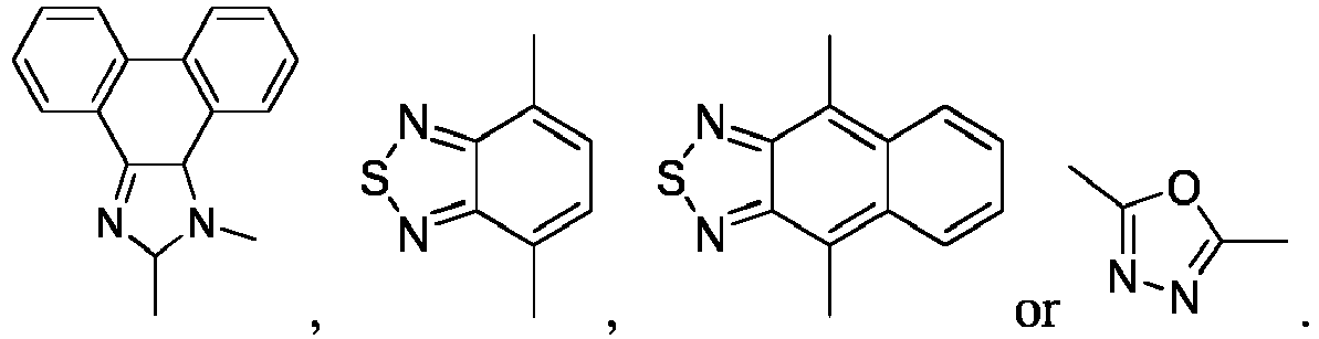
- The thermally activated and sensitized phosphorescence organic electroluminescence device according to claim 4, wherein, the thermally activated delayed fluorescence material is a compound that has the following structures:


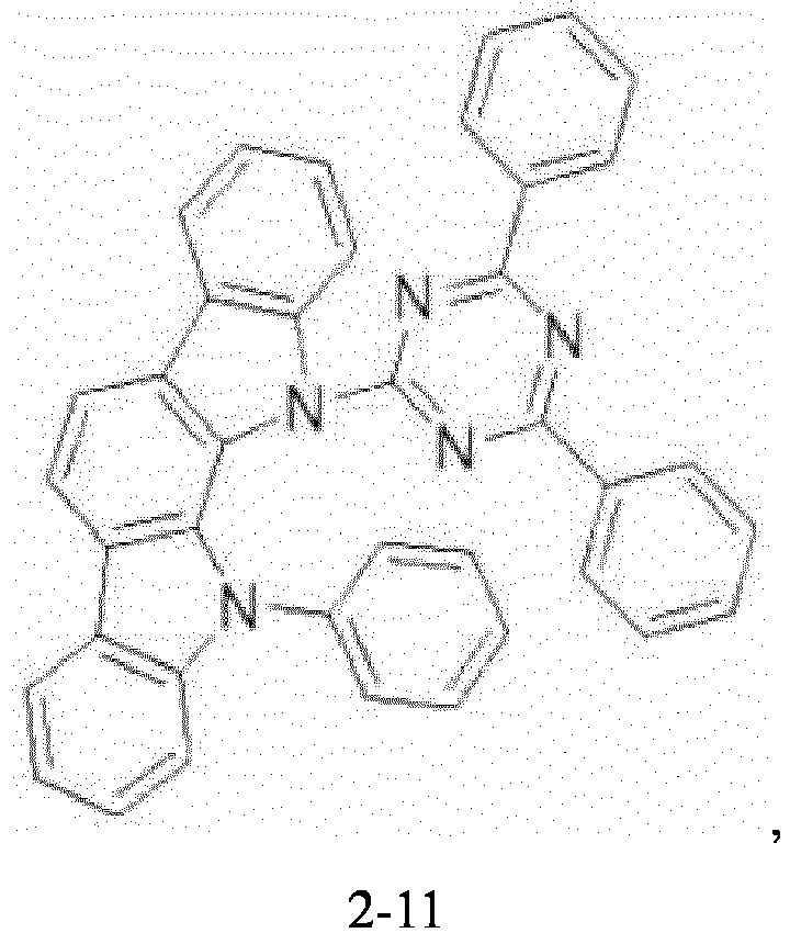


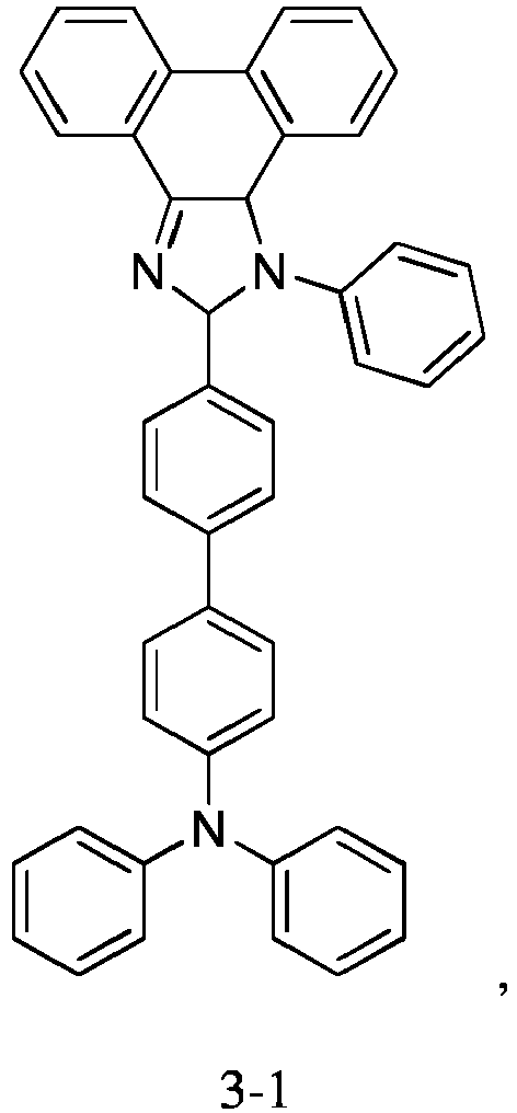


- The thermally activated and sensitized phosphorescence organic electroluminescence device according to any one of claims 1-9, wherein, both of the two materials that the host material consists of are thermally activated delayed fluorescence materials.
- The thermally activated and sensitized phosphorescence organic electroluminescence device according to any one of claims 1-9, wherein, one of the two materials that the host material consists of is a thermally activated delayed fluorescence material, and the other is a regulating host material, wherein a triplet state energy level of the thermally activated delayed fluorescence material and a triplet state energy level of the regulating host material in the host material are equal.
Applications Claiming Priority (2)
| Application Number | Priority Date | Filing Date | Title |
|---|---|---|---|
| CN201510037898.4A CN105895810B (en) | 2015-01-26 | 2015-01-26 | A kind of thermal activation sensitized phosphorescence organic electroluminescence device |
| PCT/CN2015/097529 WO2016119533A1 (en) | 2015-01-26 | 2015-12-16 | Thermally-activated sensitized phosphorescent organic electroluminescent device |
Publications (3)
| Publication Number | Publication Date |
|---|---|
| EP3226318A1 true EP3226318A1 (en) | 2017-10-04 |
| EP3226318A4 EP3226318A4 (en) | 2018-01-03 |
| EP3226318B1 EP3226318B1 (en) | 2019-04-17 |
Family
ID=56542357
Family Applications (1)
| Application Number | Title | Priority Date | Filing Date |
|---|---|---|---|
| EP15879731.6A Active EP3226318B1 (en) | 2015-01-26 | 2015-12-16 | Thermally-activated sensitized phosphorescent organic electroluminescent device |
Country Status (7)
| Country | Link |
|---|---|
| US (1) | US20180013073A1 (en) |
| EP (1) | EP3226318B1 (en) |
| JP (1) | JP6503088B2 (en) |
| KR (1) | KR101930187B1 (en) |
| CN (1) | CN105895810B (en) |
| TW (1) | TWI650403B (en) |
| WO (1) | WO2016119533A1 (en) |
Cited By (4)
| Publication number | Priority date | Publication date | Assignee | Title |
|---|---|---|---|---|
| CN109088008A (en) * | 2018-08-23 | 2018-12-25 | 京东方科技集团股份有限公司 | A kind of organic luminescent device and display panel |
| EP3565018A1 (en) * | 2018-05-04 | 2019-11-06 | cynora GmbH | Organic electroluminescent device emitting blue light |
| US11145827B2 (en) | 2015-08-07 | 2021-10-12 | Semiconductor Energy Laboratory Co., Ltd. | Light-emitting element, display device, electronic device, and lighting device |
| WO2022058502A1 (en) * | 2020-09-18 | 2022-03-24 | Cynora Gmbh | Organic electroluminescent device |
Families Citing this family (32)
| Publication number | Priority date | Publication date | Assignee | Title |
|---|---|---|---|---|
| KR101803537B1 (en) * | 2012-02-09 | 2017-11-30 | 가부시키가이샤 한도오따이 에네루기 켄큐쇼 | Light-emitting element |
| WO2016051309A1 (en) * | 2014-09-30 | 2016-04-07 | Semiconductor Energy Laboratory Co., Ltd. | Light-emitting element, display device, electronic device, and lighting device |
| US10700288B2 (en) * | 2015-07-24 | 2020-06-30 | Semiconductor Energy Laboratory Co., Ltd. | Light-emitting element, light-emitting device, electronic device, lighting device, and lighting system |
| CN107785492B (en) * | 2016-08-29 | 2020-01-10 | 昆山工研院新型平板显示技术中心有限公司 | Organic light emitting display device and display apparatus |
| CN108011047B (en) * | 2016-10-27 | 2020-03-10 | 昆山工研院新型平板显示技术中心有限公司 | Red light organic electroluminescent device |
| CN106410053B (en) * | 2016-10-31 | 2019-01-18 | 昆山工研院新型平板显示技术中心有限公司 | A kind of white light organic electroluminescent device |
| CN108011040B (en) * | 2016-10-31 | 2020-07-17 | 昆山工研院新型平板显示技术中心有限公司 | Green light organic electroluminescent device |
| KR102498770B1 (en) * | 2016-12-27 | 2023-02-10 | 닛테츠 케미컬 앤드 머티리얼 가부시키가이샤 | Materials for organic electroluminescent devices and organic electroluminescent devices |
| CN108264479B (en) * | 2016-12-30 | 2023-10-27 | 昆山国显光电有限公司 | An organic electroluminescent device |
| CN108264478B (en) * | 2016-12-30 | 2020-09-22 | 昆山国显光电有限公司 | Carrier transport material, carrier transport layer and organic light-emitting device |
| CN106816541A (en) * | 2017-01-11 | 2017-06-09 | 瑞声科技(南京)有限公司 | Phosphorescent blue oled device |
| CN109422735A (en) * | 2017-08-21 | 2019-03-05 | 邱天隆 | Carbazole derivative material and organic light-emitting diode element using same |
| CN109671850A (en) * | 2017-10-16 | 2019-04-23 | 北京鼎材科技有限公司 | A kind of organic electroluminescence device |
| CN109935723A (en) * | 2017-12-18 | 2019-06-25 | 北京鼎材科技有限公司 | A kind of organic electroluminescence device |
| CN111263986B (en) * | 2017-12-21 | 2023-04-04 | 广州华睿光电材料有限公司 | Printing ink containing thermally activated delayed fluorescence material and application thereof |
| CN110034234B (en) * | 2018-01-11 | 2023-09-05 | 北京鼎材科技有限公司 | A white light organic electroluminescent device |
| JP2021120964A (en) * | 2018-03-19 | 2021-08-19 | 出光興産株式会社 | Organic electroluminescent element and electronic apparatus |
| KR102637792B1 (en) | 2018-03-22 | 2024-02-19 | 삼성디스플레이 주식회사 | Organic light emitting device and electronic device including the same |
| TW201942327A (en) * | 2018-03-29 | 2019-11-01 | 國立大學法人九州大學 | Phosphorescent substance and phosphorescent element |
| CN111372918B (en) | 2018-07-27 | 2023-09-05 | 出光兴产株式会社 | Compound, material for organic electroluminescent element, organic electroluminescent element, and electronic device |
| KR102804493B1 (en) | 2019-04-30 | 2025-05-09 | 삼성디스플레이 주식회사 | Organic light emitting device |
| CN111987228B (en) * | 2019-05-22 | 2025-09-19 | 三星显示有限公司 | Blue light organic electroluminescent device |
| CN110335954B (en) * | 2019-07-15 | 2020-10-27 | 吉林大学 | An efficient and stable white light organic electroluminescent device and preparation method thereof |
| CN110190200B (en) * | 2019-07-15 | 2020-07-14 | 吉林大学 | Efficient pure white light organic electroluminescent device with high color rendering index and preparation method thereof |
| US11683983B2 (en) * | 2019-10-18 | 2023-06-20 | Lg Display Co., Ltd. | Organic light emitting diode and organic light emitting device including the same |
| KR102805277B1 (en) | 2020-04-16 | 2025-05-12 | 삼성전자주식회사 | Organic light emitting device |
| KR20220034512A (en) * | 2020-09-11 | 2022-03-18 | 엘지디스플레이 주식회사 | Organic compound, and Organic light emitting diode and Organic light emitting device including the same |
| CN112054129B (en) | 2020-09-15 | 2024-04-09 | 京东方科技集团股份有限公司 | Light emitting device and display device |
| KR20220085924A (en) | 2020-12-15 | 2022-06-23 | 삼성디스플레이 주식회사 | Light emitting device and electronic apparatus comprising same |
| CN113321677B (en) * | 2021-06-30 | 2023-05-05 | 京东方科技集团股份有限公司 | Thermal-activation delay fluorescent material, organic light-emitting device and display device |
| US20230363276A1 (en) * | 2022-05-09 | 2023-11-09 | Universal Display Corporation | Organic electroluminescent materials and devices |
| CN115605036A (en) * | 2022-09-15 | 2023-01-13 | 京东方科技集团股份有限公司(Cn) | Light emitting device, display panel, manufacturing method of display panel and display device |
Family Cites Families (7)
| Publication number | Priority date | Publication date | Assignee | Title |
|---|---|---|---|---|
| KR101803537B1 (en) * | 2012-02-09 | 2017-11-30 | 가부시키가이샤 한도오따이 에네루기 켄큐쇼 | Light-emitting element |
| WO2014002629A1 (en) * | 2012-06-28 | 2014-01-03 | 新日鉄住金化学株式会社 | Organic electroluminescence element and material for organic electroluminescence element |
| JP6215842B2 (en) * | 2012-12-28 | 2017-10-18 | 出光興産株式会社 | Organic electroluminescence device |
| WO2014157610A1 (en) * | 2013-03-29 | 2014-10-02 | コニカミノルタ株式会社 | Organic electroluminescent element, lighting device, display device, light-emitting thin film and composition for organic electroluminescent element, and light-emitting method |
| JP6344382B2 (en) * | 2013-04-05 | 2018-06-20 | コニカミノルタ株式会社 | Luminescent layer forming coating liquid, organic electroluminescence element, method for producing the same, and illumination / display device |
| CN105102582B (en) * | 2013-04-08 | 2018-10-12 | 默克专利有限公司 | Organic Electroluminescent Devices |
| EP3005433B1 (en) * | 2013-06-06 | 2023-02-22 | Merck Patent GmbH | Organic electroluminescent device |
-
2015
- 2015-01-26 CN CN201510037898.4A patent/CN105895810B/en active Active
- 2015-12-15 TW TW104142048A patent/TWI650403B/en active
- 2015-12-16 EP EP15879731.6A patent/EP3226318B1/en active Active
- 2015-12-16 WO PCT/CN2015/097529 patent/WO2016119533A1/en not_active Ceased
- 2015-12-16 KR KR1020177018924A patent/KR101930187B1/en active Active
- 2015-12-16 JP JP2017553295A patent/JP6503088B2/en active Active
- 2015-12-16 US US15/544,859 patent/US20180013073A1/en not_active Abandoned
Cited By (16)
| Publication number | Priority date | Publication date | Assignee | Title |
|---|---|---|---|---|
| US11145827B2 (en) | 2015-08-07 | 2021-10-12 | Semiconductor Energy Laboratory Co., Ltd. | Light-emitting element, display device, electronic device, and lighting device |
| US12365835B2 (en) | 2015-08-07 | 2025-07-22 | Semiconductor Energy Laboratory Co., Ltd. | Light-emitting element, display device, electronic device, and lighting device |
| US11770969B2 (en) | 2015-08-07 | 2023-09-26 | Semiconductor Energy Laboratory Co., Ltd. | Light-emitting element, display device, electronic device, and lighting device |
| KR102761523B1 (en) | 2018-05-04 | 2025-02-04 | 삼성디스플레이 주식회사 | Organic Electroluminescent Device Emitting Blue Light |
| US11165035B2 (en) | 2018-05-04 | 2021-11-02 | Cynora Gmbh | Organic electroluminescent device emitting blue light |
| KR20190127581A (en) * | 2018-05-04 | 2019-11-13 | 시노라 게엠베하 | Organic Electroluminescent Device Emitting Blue Light |
| EP3565018A1 (en) * | 2018-05-04 | 2019-11-06 | cynora GmbH | Organic electroluminescent device emitting blue light |
| US11245083B2 (en) | 2018-08-23 | 2022-02-08 | Chengdu Boe Optoelectronics Technology Co., Ltd. | Organic light-emitting device and display panel |
| CN109088008A (en) * | 2018-08-23 | 2018-12-25 | 京东方科技集团股份有限公司 | A kind of organic luminescent device and display panel |
| WO2022058502A1 (en) * | 2020-09-18 | 2022-03-24 | Cynora Gmbh | Organic electroluminescent device |
| WO2022058513A1 (en) * | 2020-09-18 | 2022-03-24 | Cynora Gmbh | Organic electroluminescent device |
| WO2022058504A1 (en) * | 2020-09-18 | 2022-03-24 | Cynora Gmbh | Organic electroluminescent device |
| KR20230068397A (en) * | 2020-09-18 | 2023-05-17 | 삼성디스플레이 주식회사 | organic electroluminescent device |
| KR20230077725A (en) * | 2020-09-18 | 2023-06-01 | 삼성디스플레이 주식회사 | organic electroluminescent device |
| KR102899247B1 (en) | 2020-09-18 | 2025-12-11 | 삼성디스플레이 주식회사 | organic electroluminescent devices |
| KR102902399B1 (en) | 2020-09-18 | 2025-12-19 | 삼성디스플레이 주식회사 | organic electroluminescent devices |
Also Published As
| Publication number | Publication date |
|---|---|
| JP6503088B2 (en) | 2019-04-17 |
| CN105895810A (en) | 2016-08-24 |
| TWI650403B (en) | 2019-02-11 |
| EP3226318B1 (en) | 2019-04-17 |
| US20180013073A1 (en) | 2018-01-11 |
| TW201627471A (en) | 2016-08-01 |
| KR20170094332A (en) | 2017-08-17 |
| EP3226318A4 (en) | 2018-01-03 |
| CN105895810B (en) | 2018-11-30 |
| JP2018501668A (en) | 2018-01-18 |
| KR101930187B1 (en) | 2019-03-14 |
| WO2016119533A1 (en) | 2016-08-04 |
Similar Documents
| Publication | Publication Date | Title |
|---|---|---|
| EP3226318B1 (en) | Thermally-activated sensitized phosphorescent organic electroluminescent device | |
| EP3226320B1 (en) | Organic electroluminescent device | |
| KR101930146B1 (en) | Organic electroluminescent device and method for manufacture thereof | |
| KR102810836B1 (en) | Organic electroluminescent devices, display devices, and lighting devices | |
| CN112079767B (en) | Aromatic amine compound and organic electroluminescent device comprising same | |
| CN110892541A (en) | Light-emitting element, display including the same, lighting device, and sensor | |
| JP7589548B2 (en) | Light-emitting element material containing pyrromethene boron complex, light-emitting element, display device, and lighting device | |
| TWI766086B (en) | Compound, light-emitting element using the same, display device, and lighting device | |
| WO2012090806A1 (en) | Light emitting element material and light emitting element | |
| JP6628110B2 (en) | Organic light emitting device | |
| CN109790132A (en) | Compound and organic electroluminescent device with benzoxazole ring structure | |
| KR102664158B1 (en) | Organic compounds, organic light emitting diode and organic light emitting device haivng the compounds | |
| TWI843910B (en) | Compound, organic thin film light-emitting element, display device and lighting device | |
| JP6867460B2 (en) | Organic compounds, organic light emitting diodes containing them, and organic light emitting devices | |
| CN106898709B (en) | A red phosphorescent organic electroluminescent device | |
| CN113056471A (en) | Compound and organic light emitting diode comprising same | |
| CN115340544A (en) | Organic compound taking triazine derivative as core and organic electroluminescent device comprising organic compound | |
| CN113056468A (en) | Compound and organic light emitting device including the same | |
| CN112250667B (en) | Organic compound, application thereof and organic electroluminescent device using same | |
| WO2014007022A1 (en) | Light emitting element material and light emitting element | |
| KR20210000262A (en) | Heterocyclic compound and organic light emitting device comprising same | |
| KR20210000261A (en) | Heterocyclic compound and organic light emitting device comprising same | |
| KR20200099965A (en) | Heterocyclic compound and organic light emitting device comprising same |
Legal Events
| Date | Code | Title | Description |
|---|---|---|---|
| STAA | Information on the status of an ep patent application or granted ep patent |
Free format text: STATUS: THE INTERNATIONAL PUBLICATION HAS BEEN MADE |
|
| PUAI | Public reference made under article 153(3) epc to a published international application that has entered the european phase |
Free format text: ORIGINAL CODE: 0009012 |
|
| STAA | Information on the status of an ep patent application or granted ep patent |
Free format text: STATUS: REQUEST FOR EXAMINATION WAS MADE |
|
| 17P | Request for examination filed |
Effective date: 20170627 |
|
| AK | Designated contracting states |
Kind code of ref document: A1 Designated state(s): AL AT BE BG CH CY CZ DE DK EE ES FI FR GB GR HR HU IE IS IT LI LT LU LV MC MK MT NL NO PL PT RO RS SE SI SK SM TR |
|
| AX | Request for extension of the european patent |
Extension state: BA ME |
|
| A4 | Supplementary search report drawn up and despatched |
Effective date: 20171201 |
|
| RIC1 | Information provided on ipc code assigned before grant |
Ipc: H01L 51/50 20060101ALI20171128BHEP Ipc: H01L 51/54 20060101AFI20171128BHEP |
|
| DAV | Request for validation of the european patent (deleted) | ||
| DAX | Request for extension of the european patent (deleted) | ||
| REG | Reference to a national code |
Ref country code: DE Ref legal event code: R079 Ref document number: 602015028679 Country of ref document: DE Free format text: PREVIOUS MAIN CLASS: H01L0051500000 Ipc: H01L0051540000 |
|
| RIC1 | Information provided on ipc code assigned before grant |
Ipc: H01L 51/54 20060101AFI20181010BHEP Ipc: C09K 11/06 20060101ALI20181010BHEP Ipc: H01L 51/50 20060101ALI20181010BHEP |
|
| GRAP | Despatch of communication of intention to grant a patent |
Free format text: ORIGINAL CODE: EPIDOSNIGR1 |
|
| STAA | Information on the status of an ep patent application or granted ep patent |
Free format text: STATUS: GRANT OF PATENT IS INTENDED |
|
| INTG | Intention to grant announced |
Effective date: 20181122 |
|
| GRAS | Grant fee paid |
Free format text: ORIGINAL CODE: EPIDOSNIGR3 |
|
| GRAA | (expected) grant |
Free format text: ORIGINAL CODE: 0009210 |
|
| STAA | Information on the status of an ep patent application or granted ep patent |
Free format text: STATUS: THE PATENT HAS BEEN GRANTED |
|
| AK | Designated contracting states |
Kind code of ref document: B1 Designated state(s): AL AT BE BG CH CY CZ DE DK EE ES FI FR GB GR HR HU IE IS IT LI LT LU LV MC MK MT NL NO PL PT RO RS SE SI SK SM TR |
|
| REG | Reference to a national code |
Ref country code: GB Ref legal event code: FG4D |
|
| REG | Reference to a national code |
Ref country code: CH Ref legal event code: EP |
|
| REG | Reference to a national code |
Ref country code: DE Ref legal event code: R096 Ref document number: 602015028679 Country of ref document: DE |
|
| REG | Reference to a national code |
Ref country code: AT Ref legal event code: REF Ref document number: 1122535 Country of ref document: AT Kind code of ref document: T Effective date: 20190515 Ref country code: IE Ref legal event code: FG4D |
|
| REG | Reference to a national code |
Ref country code: NL Ref legal event code: MP Effective date: 20190417 |
|
| REG | Reference to a national code |
Ref country code: LT Ref legal event code: MG4D |
|
| PG25 | Lapsed in a contracting state [announced via postgrant information from national office to epo] |
Ref country code: NL Free format text: LAPSE BECAUSE OF FAILURE TO SUBMIT A TRANSLATION OF THE DESCRIPTION OR TO PAY THE FEE WITHIN THE PRESCRIBED TIME-LIMIT Effective date: 20190417 |
|
| PG25 | Lapsed in a contracting state [announced via postgrant information from national office to epo] |
Ref country code: AL Free format text: LAPSE BECAUSE OF FAILURE TO SUBMIT A TRANSLATION OF THE DESCRIPTION OR TO PAY THE FEE WITHIN THE PRESCRIBED TIME-LIMIT Effective date: 20190417 Ref country code: PT Free format text: LAPSE BECAUSE OF FAILURE TO SUBMIT A TRANSLATION OF THE DESCRIPTION OR TO PAY THE FEE WITHIN THE PRESCRIBED TIME-LIMIT Effective date: 20190817 Ref country code: FI Free format text: LAPSE BECAUSE OF FAILURE TO SUBMIT A TRANSLATION OF THE DESCRIPTION OR TO PAY THE FEE WITHIN THE PRESCRIBED TIME-LIMIT Effective date: 20190417 Ref country code: LT Free format text: LAPSE BECAUSE OF FAILURE TO SUBMIT A TRANSLATION OF THE DESCRIPTION OR TO PAY THE FEE WITHIN THE PRESCRIBED TIME-LIMIT Effective date: 20190417 Ref country code: HR Free format text: LAPSE BECAUSE OF FAILURE TO SUBMIT A TRANSLATION OF THE DESCRIPTION OR TO PAY THE FEE WITHIN THE PRESCRIBED TIME-LIMIT Effective date: 20190417 Ref country code: SE Free format text: LAPSE BECAUSE OF FAILURE TO SUBMIT A TRANSLATION OF THE DESCRIPTION OR TO PAY THE FEE WITHIN THE PRESCRIBED TIME-LIMIT Effective date: 20190417 Ref country code: NO Free format text: LAPSE BECAUSE OF FAILURE TO SUBMIT A TRANSLATION OF THE DESCRIPTION OR TO PAY THE FEE WITHIN THE PRESCRIBED TIME-LIMIT Effective date: 20190717 |
|
| PG25 | Lapsed in a contracting state [announced via postgrant information from national office to epo] |
Ref country code: LV Free format text: LAPSE BECAUSE OF FAILURE TO SUBMIT A TRANSLATION OF THE DESCRIPTION OR TO PAY THE FEE WITHIN THE PRESCRIBED TIME-LIMIT Effective date: 20190417 Ref country code: PL Free format text: LAPSE BECAUSE OF FAILURE TO SUBMIT A TRANSLATION OF THE DESCRIPTION OR TO PAY THE FEE WITHIN THE PRESCRIBED TIME-LIMIT Effective date: 20190417 Ref country code: BG Free format text: LAPSE BECAUSE OF FAILURE TO SUBMIT A TRANSLATION OF THE DESCRIPTION OR TO PAY THE FEE WITHIN THE PRESCRIBED TIME-LIMIT Effective date: 20190717 Ref country code: GR Free format text: LAPSE BECAUSE OF FAILURE TO SUBMIT A TRANSLATION OF THE DESCRIPTION OR TO PAY THE FEE WITHIN THE PRESCRIBED TIME-LIMIT Effective date: 20190718 Ref country code: RS Free format text: LAPSE BECAUSE OF FAILURE TO SUBMIT A TRANSLATION OF THE DESCRIPTION OR TO PAY THE FEE WITHIN THE PRESCRIBED TIME-LIMIT Effective date: 20190417 |
|
| REG | Reference to a national code |
Ref country code: AT Ref legal event code: MK05 Ref document number: 1122535 Country of ref document: AT Kind code of ref document: T Effective date: 20190417 |
|
| PG25 | Lapsed in a contracting state [announced via postgrant information from national office to epo] |
Ref country code: IS Free format text: LAPSE BECAUSE OF FAILURE TO SUBMIT A TRANSLATION OF THE DESCRIPTION OR TO PAY THE FEE WITHIN THE PRESCRIBED TIME-LIMIT Effective date: 20190817 |
|
| REG | Reference to a national code |
Ref country code: DE Ref legal event code: R097 Ref document number: 602015028679 Country of ref document: DE |
|
| PG25 | Lapsed in a contracting state [announced via postgrant information from national office to epo] |
Ref country code: RO Free format text: LAPSE BECAUSE OF FAILURE TO SUBMIT A TRANSLATION OF THE DESCRIPTION OR TO PAY THE FEE WITHIN THE PRESCRIBED TIME-LIMIT Effective date: 20190417 Ref country code: CZ Free format text: LAPSE BECAUSE OF FAILURE TO SUBMIT A TRANSLATION OF THE DESCRIPTION OR TO PAY THE FEE WITHIN THE PRESCRIBED TIME-LIMIT Effective date: 20190417 Ref country code: AT Free format text: LAPSE BECAUSE OF FAILURE TO SUBMIT A TRANSLATION OF THE DESCRIPTION OR TO PAY THE FEE WITHIN THE PRESCRIBED TIME-LIMIT Effective date: 20190417 Ref country code: EE Free format text: LAPSE BECAUSE OF FAILURE TO SUBMIT A TRANSLATION OF THE DESCRIPTION OR TO PAY THE FEE WITHIN THE PRESCRIBED TIME-LIMIT Effective date: 20190417 Ref country code: DK Free format text: LAPSE BECAUSE OF FAILURE TO SUBMIT A TRANSLATION OF THE DESCRIPTION OR TO PAY THE FEE WITHIN THE PRESCRIBED TIME-LIMIT Effective date: 20190417 Ref country code: SK Free format text: LAPSE BECAUSE OF FAILURE TO SUBMIT A TRANSLATION OF THE DESCRIPTION OR TO PAY THE FEE WITHIN THE PRESCRIBED TIME-LIMIT Effective date: 20190417 |
|
| PLBE | No opposition filed within time limit |
Free format text: ORIGINAL CODE: 0009261 |
|
| STAA | Information on the status of an ep patent application or granted ep patent |
Free format text: STATUS: NO OPPOSITION FILED WITHIN TIME LIMIT |
|
| PG25 | Lapsed in a contracting state [announced via postgrant information from national office to epo] |
Ref country code: IT Free format text: LAPSE BECAUSE OF FAILURE TO SUBMIT A TRANSLATION OF THE DESCRIPTION OR TO PAY THE FEE WITHIN THE PRESCRIBED TIME-LIMIT Effective date: 20190417 Ref country code: SM Free format text: LAPSE BECAUSE OF FAILURE TO SUBMIT A TRANSLATION OF THE DESCRIPTION OR TO PAY THE FEE WITHIN THE PRESCRIBED TIME-LIMIT Effective date: 20190417 |
|
| 26N | No opposition filed |
Effective date: 20200120 |
|
| PG25 | Lapsed in a contracting state [announced via postgrant information from national office to epo] |
Ref country code: TR Free format text: LAPSE BECAUSE OF FAILURE TO SUBMIT A TRANSLATION OF THE DESCRIPTION OR TO PAY THE FEE WITHIN THE PRESCRIBED TIME-LIMIT Effective date: 20190417 |
|
| PG25 | Lapsed in a contracting state [announced via postgrant information from national office to epo] |
Ref country code: SI Free format text: LAPSE BECAUSE OF FAILURE TO SUBMIT A TRANSLATION OF THE DESCRIPTION OR TO PAY THE FEE WITHIN THE PRESCRIBED TIME-LIMIT Effective date: 20190417 |
|
| REG | Reference to a national code |
Ref country code: CH Ref legal event code: PL |
|
| REG | Reference to a national code |
Ref country code: BE Ref legal event code: MM Effective date: 20191231 |
|
| PG25 | Lapsed in a contracting state [announced via postgrant information from national office to epo] |
Ref country code: MC Free format text: LAPSE BECAUSE OF FAILURE TO SUBMIT A TRANSLATION OF THE DESCRIPTION OR TO PAY THE FEE WITHIN THE PRESCRIBED TIME-LIMIT Effective date: 20190417 |
|
| PG25 | Lapsed in a contracting state [announced via postgrant information from national office to epo] |
Ref country code: IE Free format text: LAPSE BECAUSE OF NON-PAYMENT OF DUE FEES Effective date: 20191216 Ref country code: LU Free format text: LAPSE BECAUSE OF NON-PAYMENT OF DUE FEES Effective date: 20191216 Ref country code: ES Free format text: LAPSE BECAUSE OF FAILURE TO SUBMIT A TRANSLATION OF THE DESCRIPTION OR TO PAY THE FEE WITHIN THE PRESCRIBED TIME-LIMIT Effective date: 20190417 |
|
| PG25 | Lapsed in a contracting state [announced via postgrant information from national office to epo] |
Ref country code: CH Free format text: LAPSE BECAUSE OF NON-PAYMENT OF DUE FEES Effective date: 20191231 Ref country code: LI Free format text: LAPSE BECAUSE OF NON-PAYMENT OF DUE FEES Effective date: 20191231 Ref country code: BE Free format text: LAPSE BECAUSE OF NON-PAYMENT OF DUE FEES Effective date: 20191231 |
|
| PG25 | Lapsed in a contracting state [announced via postgrant information from national office to epo] |
Ref country code: CY Free format text: LAPSE BECAUSE OF FAILURE TO SUBMIT A TRANSLATION OF THE DESCRIPTION OR TO PAY THE FEE WITHIN THE PRESCRIBED TIME-LIMIT Effective date: 20190417 |
|
| PG25 | Lapsed in a contracting state [announced via postgrant information from national office to epo] |
Ref country code: MT Free format text: LAPSE BECAUSE OF FAILURE TO SUBMIT A TRANSLATION OF THE DESCRIPTION OR TO PAY THE FEE WITHIN THE PRESCRIBED TIME-LIMIT Effective date: 20190417 Ref country code: HU Free format text: LAPSE BECAUSE OF FAILURE TO SUBMIT A TRANSLATION OF THE DESCRIPTION OR TO PAY THE FEE WITHIN THE PRESCRIBED TIME-LIMIT; INVALID AB INITIO Effective date: 20151216 |
|
| PG25 | Lapsed in a contracting state [announced via postgrant information from national office to epo] |
Ref country code: MK Free format text: LAPSE BECAUSE OF FAILURE TO SUBMIT A TRANSLATION OF THE DESCRIPTION OR TO PAY THE FEE WITHIN THE PRESCRIBED TIME-LIMIT Effective date: 20190417 |
|
| REG | Reference to a national code |
Ref country code: DE Ref legal event code: R079 Ref document number: 602015028679 Country of ref document: DE Free format text: PREVIOUS MAIN CLASS: H01L0051540000 Ipc: H10K0085000000 |
|
| P01 | Opt-out of the competence of the unified patent court (upc) registered |
Effective date: 20230526 |
|
| PGFP | Annual fee paid to national office [announced via postgrant information from national office to epo] |
Ref country code: GB Payment date: 20251229 Year of fee payment: 11 |
|
| PGFP | Annual fee paid to national office [announced via postgrant information from national office to epo] |
Ref country code: FR Payment date: 20251230 Year of fee payment: 11 |
|
| PGFP | Annual fee paid to national office [announced via postgrant information from national office to epo] |
Ref country code: DE Payment date: 20251231 Year of fee payment: 11 |