EP3226304A1 - Semiconductor devices with an enhanced resistivity region and methods of fabrication therefor - Google Patents
Semiconductor devices with an enhanced resistivity region and methods of fabrication therefor Download PDFInfo
- Publication number
- EP3226304A1 EP3226304A1 EP16204531.4A EP16204531A EP3226304A1 EP 3226304 A1 EP3226304 A1 EP 3226304A1 EP 16204531 A EP16204531 A EP 16204531A EP 3226304 A1 EP3226304 A1 EP 3226304A1
- Authority
- EP
- European Patent Office
- Prior art keywords
- layer
- semiconductor
- region
- semiconductor layer
- gallium nitride
- Prior art date
- Legal status (The legal status is an assumption and is not a legal conclusion. Google has not performed a legal analysis and makes no representation as to the accuracy of the status listed.)
- Granted
Links
Images



Classifications
-
- H—ELECTRICITY
- H10—SEMICONDUCTOR DEVICES; ELECTRIC SOLID-STATE DEVICES NOT OTHERWISE PROVIDED FOR
- H10D—INORGANIC ELECTRIC SEMICONDUCTOR DEVICES
- H10D62/00—Semiconductor bodies, or regions thereof, of devices having potential barriers
- H10D62/80—Semiconductor bodies, or regions thereof, of devices having potential barriers characterised by the materials
- H10D62/85—Semiconductor bodies, or regions thereof, of devices having potential barriers characterised by the materials being Group III-V materials, e.g. GaAs
- H10D62/8503—Nitride Group III-V materials, e.g. AlN or GaN
-
- H—ELECTRICITY
- H10—SEMICONDUCTOR DEVICES; ELECTRIC SOLID-STATE DEVICES NOT OTHERWISE PROVIDED FOR
- H10D—INORGANIC ELECTRIC SEMICONDUCTOR DEVICES
- H10D30/00—Field-effect transistors [FET]
- H10D30/40—FETs having zero-dimensional [0D], one-dimensional [1D] or two-dimensional [2D] charge carrier gas channels
- H10D30/47—FETs having zero-dimensional [0D], one-dimensional [1D] or two-dimensional [2D] charge carrier gas channels having two-dimensional [2D] charge carrier gas channels, e.g. nanoribbon FETs or high electron mobility transistors [HEMT]
- H10D30/471—High electron mobility transistors [HEMT] or high hole mobility transistors [HHMT]
- H10D30/475—High electron mobility transistors [HEMT] or high hole mobility transistors [HHMT] having wider bandgap layer formed on top of lower bandgap active layer, e.g. undoped barrier HEMTs such as i-AlGaN/GaN HEMTs
- H10D30/4755—High electron mobility transistors [HEMT] or high hole mobility transistors [HHMT] having wider bandgap layer formed on top of lower bandgap active layer, e.g. undoped barrier HEMTs such as i-AlGaN/GaN HEMTs having wide bandgap charge-carrier supplying layers, e.g. modulation doped HEMTs such as n-AlGaAs/GaAs HEMTs
-
- H—ELECTRICITY
- H10—SEMICONDUCTOR DEVICES; ELECTRIC SOLID-STATE DEVICES NOT OTHERWISE PROVIDED FOR
- H10D—INORGANIC ELECTRIC SEMICONDUCTOR DEVICES
- H10D30/00—Field-effect transistors [FET]
- H10D30/60—Insulated-gate field-effect transistors [IGFET]
-
- H—ELECTRICITY
- H10—SEMICONDUCTOR DEVICES; ELECTRIC SOLID-STATE DEVICES NOT OTHERWISE PROVIDED FOR
- H10D—INORGANIC ELECTRIC SEMICONDUCTOR DEVICES
- H10D30/00—Field-effect transistors [FET]
- H10D30/01—Manufacture or treatment
- H10D30/015—Manufacture or treatment of FETs having heterojunction interface channels or heterojunction gate electrodes, e.g. HEMT
-
- H—ELECTRICITY
- H10—SEMICONDUCTOR DEVICES; ELECTRIC SOLID-STATE DEVICES NOT OTHERWISE PROVIDED FOR
- H10D—INORGANIC ELECTRIC SEMICONDUCTOR DEVICES
- H10D30/00—Field-effect transistors [FET]
- H10D30/01—Manufacture or treatment
- H10D30/021—Manufacture or treatment of FETs having insulated gates [IGFET]
-
- H—ELECTRICITY
- H10—SEMICONDUCTOR DEVICES; ELECTRIC SOLID-STATE DEVICES NOT OTHERWISE PROVIDED FOR
- H10D—INORGANIC ELECTRIC SEMICONDUCTOR DEVICES
- H10D30/00—Field-effect transistors [FET]
- H10D30/40—FETs having zero-dimensional [0D], one-dimensional [1D] or two-dimensional [2D] charge carrier gas channels
- H10D30/47—FETs having zero-dimensional [0D], one-dimensional [1D] or two-dimensional [2D] charge carrier gas channels having two-dimensional [2D] charge carrier gas channels, e.g. nanoribbon FETs or high electron mobility transistors [HEMT]
- H10D30/471—High electron mobility transistors [HEMT] or high hole mobility transistors [HHMT]
- H10D30/475—High electron mobility transistors [HEMT] or high hole mobility transistors [HHMT] having wider bandgap layer formed on top of lower bandgap active layer, e.g. undoped barrier HEMTs such as i-AlGaN/GaN HEMTs
-
- H—ELECTRICITY
- H10—SEMICONDUCTOR DEVICES; ELECTRIC SOLID-STATE DEVICES NOT OTHERWISE PROVIDED FOR
- H10D—INORGANIC ELECTRIC SEMICONDUCTOR DEVICES
- H10D62/00—Semiconductor bodies, or regions thereof, of devices having potential barriers
- H10D62/10—Shapes, relative sizes or dispositions of the regions of the semiconductor bodies; Shapes of the semiconductor bodies
- H10D62/102—Constructional design considerations for preventing surface leakage or controlling electric field concentration
-
- H—ELECTRICITY
- H10—SEMICONDUCTOR DEVICES; ELECTRIC SOLID-STATE DEVICES NOT OTHERWISE PROVIDED FOR
- H10D—INORGANIC ELECTRIC SEMICONDUCTOR DEVICES
- H10D62/00—Semiconductor bodies, or regions thereof, of devices having potential barriers
- H10D62/10—Shapes, relative sizes or dispositions of the regions of the semiconductor bodies; Shapes of the semiconductor bodies
- H10D62/124—Shapes, relative sizes or dispositions of the regions of semiconductor bodies or of junctions between the regions
-
- H—ELECTRICITY
- H10—SEMICONDUCTOR DEVICES; ELECTRIC SOLID-STATE DEVICES NOT OTHERWISE PROVIDED FOR
- H10D—INORGANIC ELECTRIC SEMICONDUCTOR DEVICES
- H10D62/00—Semiconductor bodies, or regions thereof, of devices having potential barriers
- H10D62/10—Shapes, relative sizes or dispositions of the regions of the semiconductor bodies; Shapes of the semiconductor bodies
- H10D62/17—Semiconductor regions connected to electrodes not carrying current to be rectified, amplified or switched, e.g. channel regions
- H10D62/213—Channel regions of field-effect devices
-
- H—ELECTRICITY
- H10—SEMICONDUCTOR DEVICES; ELECTRIC SOLID-STATE DEVICES NOT OTHERWISE PROVIDED FOR
- H10D—INORGANIC ELECTRIC SEMICONDUCTOR DEVICES
- H10D62/00—Semiconductor bodies, or regions thereof, of devices having potential barriers
- H10D62/50—Physical imperfections
- H10D62/53—Physical imperfections the imperfections being within the semiconductor body
-
- H—ELECTRICITY
- H10—SEMICONDUCTOR DEVICES; ELECTRIC SOLID-STATE DEVICES NOT OTHERWISE PROVIDED FOR
- H10D—INORGANIC ELECTRIC SEMICONDUCTOR DEVICES
- H10D62/00—Semiconductor bodies, or regions thereof, of devices having potential barriers
- H10D62/80—Semiconductor bodies, or regions thereof, of devices having potential barriers characterised by the materials
- H10D62/82—Heterojunctions
- H10D62/824—Heterojunctions comprising only Group III-V materials heterojunctions, e.g. GaN/AlGaN heterojunctions
-
- H—ELECTRICITY
- H10—SEMICONDUCTOR DEVICES; ELECTRIC SOLID-STATE DEVICES NOT OTHERWISE PROVIDED FOR
- H10D—INORGANIC ELECTRIC SEMICONDUCTOR DEVICES
- H10D62/00—Semiconductor bodies, or regions thereof, of devices having potential barriers
- H10D62/80—Semiconductor bodies, or regions thereof, of devices having potential barriers characterised by the materials
- H10D62/85—Semiconductor bodies, or regions thereof, of devices having potential barriers characterised by the materials being Group III-V materials, e.g. GaAs
- H10D62/854—Semiconductor bodies, or regions thereof, of devices having potential barriers characterised by the materials being Group III-V materials, e.g. GaAs further characterised by the dopants
-
- H—ELECTRICITY
- H10—SEMICONDUCTOR DEVICES; ELECTRIC SOLID-STATE DEVICES NOT OTHERWISE PROVIDED FOR
- H10P—GENERIC PROCESSES OR APPARATUS FOR THE MANUFACTURE OR TREATMENT OF DEVICES COVERED BY CLASS H10
- H10P14/00—Formation of materials, e.g. in the shape of layers or pillars
- H10P14/20—Formation of materials, e.g. in the shape of layers or pillars of semiconductor materials
- H10P14/32—Formation of materials, e.g. in the shape of layers or pillars of semiconductor materials characterised by intermediate layers between substrates and deposited layers
- H10P14/3202—Materials thereof
- H10P14/3214—Materials thereof being Group IIIA-VA semiconductors
- H10P14/3216—Nitrides
-
- H—ELECTRICITY
- H10—SEMICONDUCTOR DEVICES; ELECTRIC SOLID-STATE DEVICES NOT OTHERWISE PROVIDED FOR
- H10P—GENERIC PROCESSES OR APPARATUS FOR THE MANUFACTURE OR TREATMENT OF DEVICES COVERED BY CLASS H10
- H10P14/00—Formation of materials, e.g. in the shape of layers or pillars
- H10P14/20—Formation of materials, e.g. in the shape of layers or pillars of semiconductor materials
- H10P14/34—Deposited materials, e.g. layers
- H10P14/3402—Deposited materials, e.g. layers characterised by the chemical composition
- H10P14/3414—Deposited materials, e.g. layers characterised by the chemical composition being group IIIA-VIA materials
- H10P14/3416—Nitrides
-
- H—ELECTRICITY
- H10—SEMICONDUCTOR DEVICES; ELECTRIC SOLID-STATE DEVICES NOT OTHERWISE PROVIDED FOR
- H10P—GENERIC PROCESSES OR APPARATUS FOR THE MANUFACTURE OR TREATMENT OF DEVICES COVERED BY CLASS H10
- H10P30/00—Ion implantation into wafers, substrates or parts of devices
- H10P30/20—Ion implantation into wafers, substrates or parts of devices into semiconductor materials, e.g. for doping
- H10P30/202—Ion implantation into wafers, substrates or parts of devices into semiconductor materials, e.g. for doping characterised by the semiconductor materials
- H10P30/206—Ion implantation into wafers, substrates or parts of devices into semiconductor materials, e.g. for doping characterised by the semiconductor materials into Group III-V semiconductors
-
- H—ELECTRICITY
- H10—SEMICONDUCTOR DEVICES; ELECTRIC SOLID-STATE DEVICES NOT OTHERWISE PROVIDED FOR
- H10P—GENERIC PROCESSES OR APPARATUS FOR THE MANUFACTURE OR TREATMENT OF DEVICES COVERED BY CLASS H10
- H10P30/00—Ion implantation into wafers, substrates or parts of devices
- H10P30/20—Ion implantation into wafers, substrates or parts of devices into semiconductor materials, e.g. for doping
- H10P30/208—Ion implantation into wafers, substrates or parts of devices into semiconductor materials, e.g. for doping of electrically inactive species
-
- H—ELECTRICITY
- H10—SEMICONDUCTOR DEVICES; ELECTRIC SOLID-STATE DEVICES NOT OTHERWISE PROVIDED FOR
- H10P—GENERIC PROCESSES OR APPARATUS FOR THE MANUFACTURE OR TREATMENT OF DEVICES COVERED BY CLASS H10
- H10P30/00—Ion implantation into wafers, substrates or parts of devices
- H10P30/20—Ion implantation into wafers, substrates or parts of devices into semiconductor materials, e.g. for doping
- H10P30/21—Ion implantation into wafers, substrates or parts of devices into semiconductor materials, e.g. for doping of electrically active species
-
- H—ELECTRICITY
- H10—SEMICONDUCTOR DEVICES; ELECTRIC SOLID-STATE DEVICES NOT OTHERWISE PROVIDED FOR
- H10W—GENERIC PACKAGES, INTERCONNECTIONS, CONNECTORS OR OTHER CONSTRUCTIONAL DETAILS OF DEVICES COVERED BY CLASS H10
- H10W10/00—Isolation regions in semiconductor bodies between components of integrated devices
-
- H—ELECTRICITY
- H10—SEMICONDUCTOR DEVICES; ELECTRIC SOLID-STATE DEVICES NOT OTHERWISE PROVIDED FOR
- H10W—GENERIC PACKAGES, INTERCONNECTIONS, CONNECTORS OR OTHER CONSTRUCTIONAL DETAILS OF DEVICES COVERED BY CLASS H10
- H10W10/00—Isolation regions in semiconductor bodies between components of integrated devices
- H10W10/01—Manufacture or treatment
-
- H—ELECTRICITY
- H10—SEMICONDUCTOR DEVICES; ELECTRIC SOLID-STATE DEVICES NOT OTHERWISE PROVIDED FOR
- H10P—GENERIC PROCESSES OR APPARATUS FOR THE MANUFACTURE OR TREATMENT OF DEVICES COVERED BY CLASS H10
- H10P90/00—Preparation of wafers not covered by a single main group of this subclass, e.g. wafer reinforcement
- H10P90/19—Preparing inhomogeneous wafers
- H10P90/1904—Preparing vertically inhomogeneous wafers
- H10P90/1906—Preparing SOI wafers
-
- H—ELECTRICITY
- H10—SEMICONDUCTOR DEVICES; ELECTRIC SOLID-STATE DEVICES NOT OTHERWISE PROVIDED FOR
- H10W—GENERIC PACKAGES, INTERCONNECTIONS, CONNECTORS OR OTHER CONSTRUCTIONAL DETAILS OF DEVICES COVERED BY CLASS H10
- H10W10/00—Isolation regions in semiconductor bodies between components of integrated devices
- H10W10/10—Isolation regions comprising dielectric materials
- H10W10/181—Semiconductor-on-insulator [SOI] isolation regions, e.g. buried oxide regions of SOI wafers
Definitions
- Embodiments of the subject matter described herein relate generally to type III-N semiconductor devices, and more specifically to GaN transistor devices.
- a typical gallium nitride (GaN) device e.g., a GaN transistor
- GaN gallium nitride
- a typical gallium nitride (GaN) device is fabricated by depositing a nucleation layer over a base substrate, and subsequently depositing a buffer layer over the nucleation layer, where the nucleation layer functions to initiate epitaxial growth of the buffer layer.
- additional GaN material, other semiconductor layers, and other structures are formed over the buffer layer to complete the device.
- drain lag is a trapping phenomenon that originates in inherent material characteristics such as lattice mismatches at the origin of dislocations. More specifically, drain lag is at least partially caused by traps in the epitaxial material between the channel and the base substrate, where the epitaxial material includes the nucleation and buffer layers. Ideally, the nucleation and buffer layers would be electrically inactive. In practice, however, these layers may contribute significant and undesirable leakage current and output conductance, thus decreasing the performance of the GaN device.
- Embodiments of semiconductor devices and fabrication methods described herein address the issue of the undesirable tradeoff between leakage current and drain lag in a type III-N device (e.g., a gallium nitride (GaN) device) by including an enhanced resistivity region below the device channel within at least a portion of the buffer layer, the nucleation layer, and the substrate. More specifically, during fabrication of a semiconductor device (e.g., a GaN transistor), an ion implantation process is performed to implant ions into and through at least a portion of the buffer layer, and also through the underlying nucleation layer, in an embodiment. In the semiconductor device, this process may make the buffer and/or nucleation layers more highly resistive (or electrically inert), which may result in a reduction in leakage current through the buffer and/or nucleation layers.
- a type III-N device e.g., a gallium nitride (GaN) device
- an ion implantation process is performed to implant ions into and through
- iron (Fe) or carbon (C) are incorporated as active dopants (e.g., as substitutional impurities) in the device in the vicinity of the nucleation layer to reduce or prevent leakage through the buffer of the device.
- active dopants e.g., as substitutional impurities
- the presence of Fe or C as a substitutional impurity dopant may cause significantly higher drain lag. Accordingly, the use of Fe or C in this manner may present an undesirable tradeoff between drain lag and leakage current.
- embodiments of semiconductor devices described herein may have significantly lower leakage current than conventional devices without a significant increase in drain lag.
- FIG. 1 is a cross-sectional, side view of a semiconductor device 100 with an enhanced resistivity region below the device channel 109, in accordance with an example embodiment.
- the semiconductor device 100 includes a semiconductor substrate 114, isolation regions 120, and an active region 130 within which a high electron mobility transistor (HEMT) is formed.
- the transistor includes a gate electrode 140 and first and second current carrying contacts 150, 160 (e.g., source and drain contacts) formed over the substrate 114, and a channel 109 formed within the substrate 114.
- the isolation regions 120 separate the active region 130 (and the transistor) from other adjacent devices (not shown) that also may be formed in and over the semiconductor substrate 114.
- the semiconductor substrate 114 may include a base substrate 102, a nucleation layer 104, a buffer layer 106 (or “first semiconductor layer”), a channel layer 108 (or “second semiconductor layer”), a barrier layer 110, and a cap layer 112.
- the base substrate 102 includes a silicon carbide (SiC) substrate.
- the base substrate 102 may include other materials such as sapphire, silicon (Si), GaN, aluminum nitride (AlN), diamond, poly-SiC, silicon on insulator, gallium arsenide (GaAs), indium phosphide (InP), and other substantially insulating or high resistivity materials.
- the nucleation layer 104 is formed on or over the upper surface 103 of the base substrate 102.
- An embodiment of the nucleation layer 104 includes a heteroepitaxial layer formed from a material selected from AlN, GaN, aluminum gallium nitride (AlGaN), indium aluminum nitride (InAlN), indium gallium nitride (InGaN), or other suitable materials.
- the nucleation layer 104 starts at the upper surface 103 of the base substrate 102 and has a thickness in a range of about 100 angstroms to about 2000 angstroms.
- the buffer layer 106 is formed on or over the upper surface 105 of the nucleation layer 104.
- the buffer layer 106 may include one or more group III-N semiconductor layers.
- Each of the one or more semiconductor layers of the buffer layer 106 may include an epitaxially grown group III-nitride epitaxial layer.
- the group-III nitride epitaxially layers that make up the buffer layer 106 may be nitrogen (N)-face or gallium (Ga)-face material, for example.
- the semiconductor layers of the buffer layer 106 may include Si, GaAs, InP, or other suitable materials.
- the buffer layer 106 is grown epitaxially on the nucleation layer 104.
- the buffer layer 106 may include at least one AlGaN mixed crystal layer.
- the total thickness of the buffer layer 106 with all of its layers may be between about 200 angstroms and about 5,000 angstroms, although other thicknesses may be used. As will be described in more detail later, and in an embodiment, the thickness of the buffer layer 106 does not exceed a thickness through which an ion species may be implanted to form an implanted region 180 (indicated with shading in FIG. 1 ), which extends through the buffer layer 106 and the nucleation layer 104, and into the base substrate 102.
- At least a portion of the implanted region 180 comprises an "enhanced resistivity region" in which the resistivity of the buffer layer 106 may be increased by intentionally disrupting the lattice and/or introducing compensating dopants through the ion implantation process used to form the implanted region 180.
- the enhanced resistivity region may correspond to the portion of the implanted region 180 that is present within the buffer layer 106, the portion of the implanted region 180 that is present within the buffer and nucleation layers 106, 104, or the portion of the implanted region 180 that is present within the buffer and nucleation layers 106, 104 and the base substrate 102.
- Each of the at least one AlGaN mixed crystal layers of the buffer layer 106 may have a composition denoted by Al X Ga 1-X N with an aluminum mole fraction, X, that can take on values between 0 and 1.
- a limiting X value of 0 yields pure GaN while a value of 1 yields pure aluminum nitride (AlN).
- the Al X Ga 1-X N layer(s) may also be configured as one or more GaN layers where the one or more GaN layers are intentionally doped with dopants that may include Si, germanium (Ge), iron (Fe), chromium (Cr), carbon (C), magnesium (Mg) or other suitable dopants that render the buffer layer 106 substantially insulating or high resistivity.
- dopant concentration may be between about 10 17 cm -3 and about 10 19 cm -3 although other higher or lower concentrations may be used.
- the Al X Ga 1-X N layers may be configured as a superlattice where the additional layers include a series of alternating NID or doped Al X Ga 1-X N layers where the value of X takes a value between 0 and 1.
- the buffer layer 106 may also or alternatively include one or more indium gallium nitride (InGaN) layers, with composition denoted In Y Ga 1-Y N, where Y, the indium mole fraction, may take a value between 0 and 1.
- the thickness of the InGaN layer(s) may be between about 50 angstroms and about 2000 angstroms although other thicknesses may be used.
- one or more ion species are implanted into and through the buffer layer 106 and the nucleation layer 104, and into the substrate 102 to form an implanted region 180, all or a portion of which corresponds to an enhanced resistivity region.
- the term “enhanced resistivity” means having an electrical resistivity that is significantly higher than the resistivity of the buffer layer 106 without implantation of the ion species, where "significantly higher” means at least two times higher, in an embodiment, at least 10 times higher, in another embodiment, at least 100 times higher, in yet another embodiment. In still other embodiments, "significantly higher” means at least 1000 times higher.
- the resistivity of the enhanced resistivity region may be within a range of about 10 5 ohm-cm to about 10 10 ohm-cm, although the resistivity of the enhanced resistivity region may be lower or higher, as well.
- the implanted region 180 has an upper boundary 184 that substantially coincides with the upper surface 107 of the buffer layer 106, although the upper boundary may be above or below the upper surface 107 of the buffer layer 106, as well.
- the implanted region 180 has a lower boundary 182 that is located a distance below the upper surface 103 of the base substrate 102, in an embodiment.
- the lower boundary 182 of the implanted region 180 may be in a range of about 50 angstroms to about 20,000 angstroms below the upper surface 103 of the base substrate 102, although the lower boundary 182 may be located at a shallower or deeper distance below the upper surface 103 of the base substrate 102, as well.
- the lower boundary 182 may substantially coincide with the upper surface 103 of the base substrate 102, or the lower boundary 182 may be above the upper surface 103 of the base substrate 102 (e.g., the lower boundary 182 may be in the nucleation layer 104 or the buffer layer 106).
- the one or more ion species within the implanted region 180 include one or more ion species that may significantly disrupt the crystal lattice and/or introduce compensating dopants during the implantation process, resulting in a significant increase in the resistivity of the crystal lattice in the enhanced resistivity portion of the implanted region 180.
- the one or more ion species are selected from boron, arsenic, helium, beryllium, magnesium, argon, aluminum, phosphorus, nitrogen, oxygen, carbon, and iron.
- the dopant concentration of the one or more ion species within the enhanced resistivity region may be between about 10 15 cm -3 and about 10 19 cm -3 in some embodiments and may be between about 5x10 15 cm -3 and about 1x10 18 cm -3 in other embodiments, though other higher or lower concentrations may be used.
- Methods for forming the implanted region 180 will be discussed in more detail below.
- a channel layer 108 is formed on or over the upper surface 107 of the buffer layer 106 and the implanted region 180.
- the channel layer 108 may include one or more group III-N semiconductor layers.
- the channel layer 108 may include an Al X Ga 1-X N layer where X takes on values between 0 and 1.
- the thickness of the channel layer 108 may be between about 100 angstroms and about 10.0 microns, or between about 1000 angstroms to about 5000 angstroms, or between about 1000 angstroms to about 1.0 microns, although other thicknesses alternatively may be used.
- the channel layer 108 may be NID or, alternatively, may include Si, Ge, C, Fe, Cr, Mg, or other suitable dopants.
- the dopant concentration may be between about 10 16 cm -3 and about 10 19 cm -3 although other higher or lower concentrations may be used.
- the channel layer may include NID or doped In Y Ga 1-Y N, where Y, the indium mole fraction, may take a value between 0 and 1.
- a barrier layer 110 is formed on or over the channel layer 108 in accordance with an embodiment.
- the barrier layer 110 may include one or more group III-N semiconductor layers.
- the barrier layer 110 has a larger bandgap and larger spontaneous polarization than the channel layer 108 and, when the barrier layer 110 is in direct contact with the channel layer 108, a channel 109 is created in the form of a two dimensional electron gas (2-DEG) within the channel layer 108 near the interface between the channel layer 108 and barrier layer 110.
- strain between the barrier layer 110 and channel layer 108 may cause additional piezoelectric charge to be introduced into the 2-DEG and channel.
- the barrier layer 110 may include at least one NID Al X Ga 1-X N layer where X takes on values between 0 and 1.
- X may take a value of 0.1 to 0.35, although other values of X may be used.
- the thickness of the barrier layer 110 may be between about 50 angstroms and about 1000 angstroms although other thicknesses may be used.
- the barrier layer 110 may be NID or, alternatively, may include Si, Ge, C, Fe, Cr, Mg, or other suitable dopants.
- the dopant concentration may be between about 10 16 cm -3 and about 10 19 cm -3 , although other higher or lower concentrations may be used.
- the AlN interbarrier layer may increase the channel charge and improve the electron confinement of the resultant 2-DEG.
- the barrier layer 110 may include indium aluminum nitride (InAlN) layers, denoted In Y Al 1-Y N, where Y, the indium mole fraction, may take a value between about 0.1 and about 0.2 although other values of Y may be used.
- the thickness of the barrier layer 110 may be between about 50 angstroms and about 2000 angstroms, although other thicknesses may be used.
- the InAlN may be NID or, alternatively, may include Si, Ge, C, Fe, Cr, Mg, or other suitable dopants.
- the dopant concentration may be between about 10 16 cm -3 and about 10 19 cm -3 although other higher or lower concentrations may be used.
- the upper boundary 184 of the implanted region 180 is located a distance 186 below the channel 109 and the upper surface of the channel layer 108.
- a region of semiconductor material between the upper boundary 184 of the implanted region 180 and the channel 109 does not include a significant concentration of the ion species introduced into the substrate 114 to be classified as an enhanced resistivity region.
- a cap layer 112 may be formed on or over the barrier layer 110.
- the cap layer 112 presents a stable surface for the semiconductor substrate 114 and serves to protect the surface of the semiconductor substrate 114 from chemical and environmental exposure incidental to wafer processing.
- the cap layer 112 may include one or more group III-N semiconductor layers.
- the cap layer 112 is GaN.
- the thickness of the cap layer 112 may be between about 5 angstroms and about 100 angstroms, although other thicknesses may be used.
- the cap layer 112 may be NID or, alternatively, may include Si, Ge, C, Fe, Cr, Mg, or other suitable dopants.
- the dopant concentration may be between about 10 16 cm -3 and about 10 19 cm -3 although other higher or lower concentrations may be used.
- the choice of materials and arrangement of layers to form semiconductor substrate 114 is exemplary.
- the inclusion of the base substrate 102, a nucleation layer 104, a buffer layer 106, a channel layer 108, a barrier layer 110, and a cap layer 112 into the semiconductor substrate 114 is exemplary and that the function and operation of the various layers may be combined and may change depending on the materials used in any specific embodiment.
- the channel layer 108 may be disposed over the barrier layer 110 to create a 2-DEG and channel directly underneath an optional cap 112 and gate electrode 140.
- Still further embodiments may include semiconductor layers formed from materials including GaAs, aluminum gallium arsenide (AlGaAs), indium gallium arsenide (InGaAs), and aluminum indium arsenide (AlInAs) to form the semiconductor substrate 114.
- AlGaAs aluminum gallium arsenide
- InGaAs indium gallium arsenide
- AlInAs aluminum indium arsenide
- isolation regions 120 may be formed in the semiconductor substrate 114 to define an active region 130 along upper surface of the semiconductor substrate 114, according to an embodiment.
- the isolation regions 120 may be formed via an implantation procedure configured to damage the epitaxial and/or other semiconductor layers to create high resistivity regions 122 of the semiconductor substrate 114, rendering the semiconductor substrate 114 high resistivity or semi-insulating in those high resistivity regions 122 while leaving the crystal structure intact in the active region 130.
- isolation regions 120 may be formed by implanting an ion species at an energy sufficient to drive the species through cap layer 112, barrier layer 110, channel layer 108, and buffer layer 106 thus damaging the crystal lattice for these layers, disrupting channel 109 within the isolation regions 120, and creating high resistivity regions 122 within semiconductor substrate 114.
- the isolation regions 120 may be formed by removing one or more of the epitaxial and/or other semiconductor layers of the semiconductor substrate 114, rendering the remaining layers of the semiconductor substrate 114 semi-insulating and leaving behind active region 130 "mesas" surrounded by high resistivity or semi-insulating isolation regions 120.
- a first dielectric layer 124 may be formed over the active region 130 and isolation regions 120.
- the first dielectric layer 124 may include one of Si 3 N 4 , silicon dioxide (SiO 2 ), silicon oxynitride (SiON), Al 2 O 3 , hafnium dioxide (HfO 2 ), a combination of these, or other suitable insulating dielectric layers.
- an opening is made in the first dielectric layer 124, and a gate electrode 140 is formed over the semiconductor substrate 114 in the active region 130.
- the gate electrode 140 is electrically coupled to the channel 109 through the cap layer 112 and barrier layer 110. Changes to the electric potential on the gate electrode 140 shifts the quasi Fermi level for the barrier layer 110 compared to the quasi Fermi level for the channel layer 108 and thereby modulates the electron concentration in the channel 109 within the semiconductor substrate 114 under the gate electrode 140.
- the gate electrode 140 may be configured as a Schottky gate, for example, and may be formed over and directly in contact with the cap layer 112 of the semiconductor substrate 114 using a Schottky material layer and a conductive metal layer.
- a conductive low stress metal may be deposited over the Schottky material layer to form gate electrode 140, in an embodiment.
- the gate electrode 140 may be T-shaped with a vertical stem, as shown, or may be a square shape in other embodiments.
- the gate electrode 140 may be recessed through the cap layer 112 and extend partially into the barrier layer 110, increasing the electrical coupling of the gate electrode 140 to the channel 109 through the barrier layer 110.
- the gate electrode 140 may be formed over a gate dielectric or gate oxide forming a metal-insulator-semiconductor (MIS) junction or metal oxide semiconductor (MOS) junction, electrically coupling to the channel 109 through the dielectric or oxide layer.
- MIS metal-insulator-semiconductor
- MOS metal oxide semiconductor
- a first current carrying contact 150 (e.g., a source or a drain contact) may be formed over and in contact with the semiconductor substrate 114 adjacent the gate electrode 140 in the active region 130.
- the first current carrying contact 150 may form an ohmic electrode with an ohmic junction to the channel 109.
- the first current carrying contact 150 may be formed over and in contact with the cap layer 112.
- the first current carrying contact 150 may be recessed through the cap layer 112 and may extend partially through the barrier layer 110.
- ion implantation may be used to form ohmic contact to the channel 109.
- a second current carrying contact 160 may be formed over and in contact with the semiconductor substrate 114 adjacent the gate electrode 140 in the active region 130.
- the second current carrying contact 160 may form a Schottky junction with the channel 109, thus acting as a Schottky diode incorporated into the second current carrying contact 160.
- the second current carrying contact 160 may be formed over and in contact with the cap layer 112.
- the second current carrying contact 160 may be recessed through the cap layer 112 and extend partially through the barrier layer 110 to form a Schottky junction.
- metal electrodes may be formed on or over the first and second current carrying contacts 150, 160 in the active region 130.
- one or more additional dielectric layers may be formed over the metal electrodes, the gate electrode 140, the first and second current carrying contact 150, 160, and the first dielectric layer 124 in the isolation regions 120 and the active region 130.
- the additional dielectric layer(s) encapsulate the active region 130 and the isolation regions 120, protecting the surface from moisture and other contaminants. Additional metal electrodes, dielectric layers, and patterned metal layers also may be formed to provide desired electrical connectivity to the transistor device within the active region 130.
- the enhanced resistivity region of the implanted region 180 may address the issue of the undesirable tradeoff between leakage current and drain lag in a conventional type III-N device (e.g., a gallium nitride (GaN) device) by making at least the buffer and/or nucleation layers more electrically resistive or inert, when compared with their resistivity prior to the ion implantation process. This may result in a reduction in leakage current through the buffer and/or nucleation layers.
- a leakage path that may be present in a conventional device i.e., a device that does not include an implanted region 180
- substantially less leakage current may travel through the buffer layer 106, thus improving performance of device 100 in comparison to conventional devices.
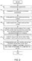
- FIG. 2 is a flowchart of a method for fabricating a semiconductor device with an enhanced resistivity region, in accordance with an example embodiment.
- FIG. 2 should be viewed in conjunction with FIGs 3-6 , which illustrate cross-sectional, side views of a series of fabrication steps for producing the semiconductor device of FIG. 1 , in accordance with an example embodiment.
- the method may begin, in block 202, by providing a base substrate 102.
- the base substrate 102 may include SiC, or may include other materials such as sapphire, Si, GaN, AlN, diamond, poly-SiC, silicon on insulator, GaAs, InP, or other substantially insulating or high resistivity materials.
- a nucleation layer 104 is formed on or over the upper surface 103 of the base substrate 102.
- an embodiment of the nucleation layer 104 includes a heteroepitaxial layer formed from a material selected from AlN, GaN, AlGaN, InAlN, InGaN, or other suitable materials.
- the nucleation layer 104 starts at the upper surface 103 of the base substrate 102 and has a thickness 304 in a range of about 100 angstroms to about 2000 angstroms.
- the nucleation layer 104 may be grown on or over the upper surface 103 of base substrate 102 using one of metal-organo chemical vapor deposition (MOCVD), molecular beam epitaxy (MBE), hydride-vapor phase epitaxy (HVPE) or a combination of these techniques, although other suitable techniques alternatively may be used.
- MOCVD metal-organo chemical vapor deposition
- MBE molecular beam epitaxy
- HVPE hydride-vapor phase epitaxy
- a buffer layer 106 (also referred to as a "first semiconductor layer”) is formed on or over the upper surface 105 of the nucleation layer 104.
- the buffer layer 106 may include one or more group III-N semiconductor layers, including an epitaxially grown group III-nitride epitaxial layer (e.g., nitrogen (N)-face or gallium (Ga)-face materials), or alternatively may include Si, GaAs, InP, or other suitable materials.
- the buffer layer 106 may include at least one AlGaN mixed crystal layer.
- the buffer layer 106 is grown epitaxially on the upper surface 105 of the nucleation layer 104.
- the total thickness 306 of the buffer layer 106 may be between about 200 angstroms and about 20,000 angstroms, although other thicknesses may be used.
- the buffer layer 106 may be grown on or over the upper surface 105 of the nucleation layer 104 using one of MOCVD, MBE, HVPE or a combination of these techniques, although other suitable techniques alternatively may be used.
- the thickness 306 of the buffer layer 106 does not exceed a thickness through which an ion species may be implanted through the entire depth of the buffer layer 106 to form an implanted region 180 that includes an enhanced resistivity region ( FIGs 1 , 4 ).
- a sacrificial dielectric layer 310 optionally is formed on or over the upper surface of the buffer layer 106.
- the sacrificial dielectric layer 310 may function to protect the surface of the buffer layer 106 from exposure to contaminants that may be present in the atmosphere during subsequent processing steps (e.g., before and during the ion implantation process of block 210).
- the sacrificial dielectric layer 310 may include one of Si 3 Na, SiO 2 , SiON, Al 2 O 3 , HfO 2 , polycrystaline AlN, a combination of these, or other suitable dielectric layers.
- the total thickness of the layers used to form sacrificial dielectric layer 310 may be between about 30 and about 10,000 angstroms in thickness, although other thickness values may be used.
- the sacrificial dielectric layer 310 may be deposited using low pressure chemical vapor deposition (LPCVD), plasma-enhanced chemical vapor deposition (PECVD), sputtering, physical vapor deposition (PVD), atomic layer deposition (ALD), catalytic chemical vapor deposition (Cat-CVD), hot-wire chemical vapor deposition (HWCVD), electron-cyclotron resonance (ECR) CVD, inductively coupled plasma (ICP) CVD, a combination of these or other suitable dielectric deposition technique(s).
- LPCVD low pressure chemical vapor deposition
- PECVD plasma-enhanced chemical vapor deposition
- PVD physical vapor deposition
- ALD atomic layer deposition
- Cat-CVD catalytic chemical vapor deposition
- HWCVD hot-wire chemical vapor deposition
- ECR electron-cyclotron resonance
- ICP inductively coupled plasma
- the method may continue, in block 210, by implanting ions (indicated by arrows 410) of a suitable species (i.e., a species that enhances the resistivity of buffer layer 106 by disrupting the crystal lattice and/or introducing compensating dopants as a result of the implantation process) through the dielectric layer 310 (if included), the buffer layer 106, and the nucleation layer 104, and into the base substrate 102 to form an implanted region 180 that includes an enhanced resistivity region, in an embodiment.
- a suitable species i.e., a species that enhances the resistivity of buffer layer 106 by disrupting the crystal lattice and/or introducing compensating dopants as a result of the implantation process
- the one or more ion species within the implanted region 180 are selected from boron, arsenic, helium, beryllium, magnesium, argon, aluminum, phosphorus, nitrogen, oxygen, carbon, and iron. Other suitable ion species may be used, as well.
- the dopant concentration of the one or more ion species within the implanted region 180 may be between about 10 15 cm -3 and about 10 19 cm -3 or, in some embodiments, between about 5x10 15 cm -3 and about 1x10 18 cm -3 though other higher or lower concentrations may be used.
- the implant energy and acceleration voltage used to implant the ions are sufficient to ensure substantial penetration of the ions through the various layers to a desired depth.
- the acceleration voltage used to implant the ions may be in a range of about 50 kilovolts to about 200 kilovolts, although lower or higher acceleration voltages alternatively may be used.
- the implanted region 180 has a lower boundary 182 that is located a distance 480 below the upper surface 103 of the base substrate 102, in an embodiment.
- the lower boundary 182 of the implanted region 180 may be in a range of 50 angstroms to about 20,000 angstroms below the upper surface 103 of the base substrate 102, although the lower boundary 182 may be located at a shallower or deeper distance below the upper surface 103 of the base substrate 102, as well.
- the lower boundary 182 may substantially coincide with the upper surface 103 of the base substrate 102, or the lower boundary 182 may be above the upper surface 103 of the base substrate 102 (e.g., the lower boundary 182 may be in the nucleation layer 104 or the buffer layer 106).
- the dielectric layer 310 (if included) is removed, in block 212, and a channel layer 108 is formed on or over the upper surface 107 of the buffer layer 106 and the implanted region 180.
- the channel layer 108 may include one or more group III-N semiconductor layers (e.g., including high quality NID GaN).
- the channel layer 108 may be grown on or over the upper surface 107 of the buffer layer 106 using one of MOCVD, MBE, HVPE or a combination of these techniques, although other suitable techniques alternatively may be used.
- the thickness 508 of the channel layer 108 may be between about 100 angstroms and about 10.0 microns, or between about 1000 angstroms to about 5000 angstroms, or between about 1000 angstroms to about 1.0 microns, although other thicknesses alternatively may be used.
- the implantation process used to create the implanted region 180 with the enhanced resistivity region is performed before formation of the channel layer 108.
- both the buffer and channel layers 106, 108 may be formed, and the implantation process may be performed thereafter.
- the implantation procedure would be performed to bury the implanted region 180 below the upper surface of the channel layer 108.
- additional semiconductor layers and structures are formed, in block 214, to complete the semiconductor device 100.
- this may include forming a barrier layer 110 on or over the channel layer 108 (resulting in the creation of a channel 109 in the form of a 2-DEG), and forming a cap layer 112 on or over the barrier layer 110.
- Conventional semiconductor processing techniques may be used to form the barrier and cap layers 110, 112, and such techniques are not described in detail herein for the purpose of brevity.
- Additional processes for completing the semiconductor device 100 may include forming one or more isolation regions 120 to define an active region 130 along upper surface of the semiconductor substrate 114, forming a first dielectric layer 124 over at least the active region 130, forming a gate electrode 140, and forming first and second current carrying contacts 150, 160 (e.g., source and drain contacts). Additional metal electrodes, dielectric layers, and patterned metal layers (not illustrated) also may be formed to provide desired electrical connectivity to the transistor device within the active region 130.
- conventional semiconductor processing techniques may be used to form the isolation regions 120, the first dielectric layer 124, the gate electrode 140, the current carrying contacts 150, 160, and the additional structures, and such techniques are not described in detail herein for the purpose of brevity.
- Embodiments of a semiconductor device include a base substrate including an upper surface, a nucleation layer disposed over the upper surface of the base substrate, a first semiconductor layer disposed over the nucleation layer, a second semiconductor layer disposed over the first semiconductor layer, a channel within the second semiconductor layer and proximate to an upper surface of the second semiconductor layer, and an implanted region in which one or more ion species are implanted.
- the implanted region includes an enhanced resistivity region, and the implanted region has an upper boundary located a distance below the channel and the upper surface of the second semiconductor layer.
- the implanted region extends through the first semiconductor layer. In an example, the implanted region also extends through the nucleation layer. In an example, the implanted region also extends into a portion of the base substrate.
- the enhanced resistivity region is present within the buffer layer. In an example, the enhanced resistivity region also extends into the nucleation region.
- the nucleation layer comprises a heteroepitaxial layer formed from a material selected from aluminum nitride, gallium nitride, aluminum gallium nitride, indium gallium nitride, and indium aluminum nitride.
- the first and second semiconductor layers comprise not intentionally doped gallium nitride.
- the one or more ion species are selected from boron, arsenic, helium, beryllium, magnesium, argon, aluminum, and phosphorus.
- the one or more ion species are selected from nitrogen, oxygen, carbon, and iron.
- the ion species have a concentration within the enhanced resistivity region between 5x10 15 cm -3 and 1x10 18 cm -3 .
- the semiconductor device further comprises a source contact and a drain contact formed over the second semiconductor layer and electrically coupled to the channel; and a gate electrode disposed over the second semiconductor layer between the source contact and the drain contact and electrically coupled to the channel.
- a semiconductor device include a base substrate including an upper surface, a nucleation layer disposed over the base substrate, a first gallium nitride layer disposed over the nucleation layer, an enhanced resistivity region with an upper boundary proximate to an upper surface of the first gallium nitride layer, a second gallium nitride layer disposed over the first gallium nitride layer and the enhanced resistivity region, and a channel within a portion of the second gallium nitride layer overlying the enhanced resistivity region and proximate to an upper surface of the second gallium nitride layer.
- the base substrate comprises a material selected from silicon carbide (SiC), sapphire, silicon, gallium nitride, aluminum nitride, diamond, poly-SiC, silicon on insulator, gallium arsenide, and indium phosphide.
- the nucleation layer comprises a heteroepitaxial layer formed from a material selected from aluminum nitride, and aluminum gallium nitride.
- the one or more ion species are selected from boron, arsenic, helium, beryllium, magnesium, argon, aluminum, phosphorus, nitrogen, oxygen, carbon, and iron.
- the ion species have a concentration within the enhanced resistivity region between 5x10 15 cm -3 and 1x10 18 cm -3 .
- Embodiments of a method of fabricating a semiconductor device include forming a nucleation layer over an upper surface of a base substrate, forming a first semiconductor layer over the nucleation layer, and implanting one or more ion species through the first semiconductor layer to form an enhanced resistivity region with an upper boundary proximate to an upper surface of the first semiconductor layer.
- the enhanced resistivity region comprises at least a portion of the first semiconductor layer.
- the method further includes forming a second semiconductor layer over the first semiconductor layer and the enhanced resistivity region, and forming a channel within a portion of the second semiconductor layer overlying the enhanced resistivity region and proximate to an upper surface of the second semiconductor layer.
- the nucleation layer comprises a heteroepitaxial layer formed from a material selected from aluminum nitride, and aluminum gallium nitride.
- the first and second semiconductor layers comprise gallium nitride.
- the one or more ion species are selected from boron, arsenic, helium, beryllium, magnesium, argon, aluminum, phosphorus, nitrogen, oxygen, carbon, and iron.
- the ion species are implanted to a concentration within the enhanced resistivity region between 5x10 15 cm -3 and 1x10 18 cm -3 .
- implanting the one or more ion species comprises implanting the one or more ion species at an acceleration voltage between 50 kilovolts and 200 kilovolts.
- the method further comprises after the step of forming the first semiconductor layer and before the step of implanting the one or more ion species, forming a dielectric layer over the upper surface of the first semiconductor layer; and after the step of implanting the one or more ion species, removing at least a portion of the dielectric layer.
- the method further comprises forming a source contact and a drain contact over the second semiconductor layer and electrically coupled to the channel; and forming a gate electrode over the second semiconductor layer between the source contact and the drain contact and electrically coupled to the channel.
- a HEMT device with an enhanced resistivity region below the channel may include more and/or different semiconductor layers and/or other electrically-active or electrically-inactive structures.
- an enhanced resistivity region may be incorporated into a HEMT device with a channel in the form of a two dimensional hole gas (2-DHG) near the interface between the channel and barrier layers, in other embodiments.
- an enhanced resistivity region may be incorporated into a device other than a HEMT device, including but not limited to metal semiconductor field effect transistors (MESFET's) and metal-oxide semiconductor field effect transistors (MOSFET's).
- MESFET's metal semiconductor field effect transistors
- MOSFET's metal-oxide semiconductor field effect transistors
Landscapes
- Junction Field-Effect Transistors (AREA)
- Insulated Gate Type Field-Effect Transistor (AREA)
Abstract
Description
- Embodiments of the subject matter described herein relate generally to type III-N semiconductor devices, and more specifically to GaN transistor devices.
- A typical gallium nitride (GaN) device (e.g., a GaN transistor) is fabricated by depositing a nucleation layer over a base substrate, and subsequently depositing a buffer layer over the nucleation layer, where the nucleation layer functions to initiate epitaxial growth of the buffer layer. After deposition of the nucleation and buffer layers, additional GaN material, other semiconductor layers, and other structures (e.g., gate, drain, and source contacts) are formed over the buffer layer to complete the device.
- A memory effect referred to as "drain lag" is a significant issue in GaN semiconductor devices. Drain lag is a trapping phenomenon that originates in inherent material characteristics such as lattice mismatches at the origin of dislocations. More specifically, drain lag is at least partially caused by traps in the epitaxial material between the channel and the base substrate, where the epitaxial material includes the nucleation and buffer layers. Ideally, the nucleation and buffer layers would be electrically inactive. In practice, however, these layers may contribute significant and undesirable leakage current and output conductance, thus decreasing the performance of the GaN device.
- A more complete understanding of the subject matter may be derived by referring to the detailed description and claims when considered in conjunction with the following figures, wherein like reference numbers refer to similar elements throughout the figures.
-
FIG. 1 is a cross-sectional, side view of a semiconductor device with an enhanced resistivity region, in accordance with an example embodiment; -
FIG. 2 is a flowchart of a method for fabricating a semiconductor device with an enhanced resistivity region, in accordance with an example embodiment; and -
FIGs 3-6 illustrate cross-sectional, side views of a series of fabrication steps for producing the semiconductor device ofFIG. 1 , in accordance with an example embodiment. - Embodiments of semiconductor devices and fabrication methods described herein address the issue of the undesirable tradeoff between leakage current and drain lag in a type III-N device (e.g., a gallium nitride (GaN) device) by including an enhanced resistivity region below the device channel within at least a portion of the buffer layer, the nucleation layer, and the substrate. More specifically, during fabrication of a semiconductor device (e.g., a GaN transistor), an ion implantation process is performed to implant ions into and through at least a portion of the buffer layer, and also through the underlying nucleation layer, in an embodiment. In the semiconductor device, this process may make the buffer and/or nucleation layers more highly resistive (or electrically inert), which may result in a reduction in leakage current through the buffer and/or nucleation layers.
- In some devices, in order to reduce leakage current, iron (Fe) or carbon (C) are incorporated as active dopants (e.g., as substitutional impurities) in the device in the vicinity of the nucleation layer to reduce or prevent leakage through the buffer of the device. Unfortunately, however, the presence of Fe or C as a substitutional impurity dopant may cause significantly higher drain lag. Accordingly, the use of Fe or C in this manner may present an undesirable tradeoff between drain lag and leakage current. By including an enhanced resistivity region in the semiconductor material below the device channel by intentionally disrupting the lattice and/or introducing compensating dopants using ion implantation, embodiments of semiconductor devices described herein may have significantly lower leakage current than conventional devices without a significant increase in drain lag.
-
FIG. 1 is a cross-sectional, side view of asemiconductor device 100 with an enhanced resistivity region below thedevice channel 109, in accordance with an example embodiment. Thesemiconductor device 100 includes asemiconductor substrate 114,isolation regions 120, and anactive region 130 within which a high electron mobility transistor (HEMT) is formed. The transistor includes agate electrode 140 and first and secondcurrent carrying contacts 150, 160 (e.g., source and drain contacts) formed over thesubstrate 114, and achannel 109 formed within thesubstrate 114. Theisolation regions 120 separate the active region 130 (and the transistor) from other adjacent devices (not shown) that also may be formed in and over thesemiconductor substrate 114. - The
semiconductor substrate 114 may include abase substrate 102, anucleation layer 104, a buffer layer 106 (or "first semiconductor layer"), a channel layer 108 (or "second semiconductor layer"), abarrier layer 110, and acap layer 112. In an embodiment, thebase substrate 102 includes a silicon carbide (SiC) substrate. In other embodiments, thebase substrate 102 may include other materials such as sapphire, silicon (Si), GaN, aluminum nitride (AlN), diamond, poly-SiC, silicon on insulator, gallium arsenide (GaAs), indium phosphide (InP), and other substantially insulating or high resistivity materials. - The
nucleation layer 104 is formed on or over theupper surface 103 of thebase substrate 102. An embodiment of thenucleation layer 104 includes a heteroepitaxial layer formed from a material selected from AlN, GaN, aluminum gallium nitride (AlGaN), indium aluminum nitride (InAlN), indium gallium nitride (InGaN), or other suitable materials. Thenucleation layer 104 starts at theupper surface 103 of thebase substrate 102 and has a thickness in a range of about 100 angstroms to about 2000 angstroms. - The
buffer layer 106 is formed on or over theupper surface 105 of thenucleation layer 104. According to an embodiment, thebuffer layer 106 may include one or more group III-N semiconductor layers. Each of the one or more semiconductor layers of thebuffer layer 106 may include an epitaxially grown group III-nitride epitaxial layer. The group-III nitride epitaxially layers that make up thebuffer layer 106 may be nitrogen (N)-face or gallium (Ga)-face material, for example. In still other embodiments, the semiconductor layers of thebuffer layer 106 may include Si, GaAs, InP, or other suitable materials. - In an embodiment, the
buffer layer 106 is grown epitaxially on thenucleation layer 104. Thebuffer layer 106 may include at least one AlGaN mixed crystal layer. The total thickness of thebuffer layer 106 with all of its layers may be between about 200 angstroms and about 5,000 angstroms, although other thicknesses may be used. As will be described in more detail later, and in an embodiment, the thickness of thebuffer layer 106 does not exceed a thickness through which an ion species may be implanted to form an implanted region 180 (indicated with shading inFIG. 1 ), which extends through thebuffer layer 106 and thenucleation layer 104, and into thebase substrate 102. At least a portion of the implantedregion 180 comprises an "enhanced resistivity region" in which the resistivity of thebuffer layer 106 may be increased by intentionally disrupting the lattice and/or introducing compensating dopants through the ion implantation process used to form the implantedregion 180. In various embodiments, the enhanced resistivity region may correspond to the portion of the implantedregion 180 that is present within thebuffer layer 106, the portion of the implantedregion 180 that is present within the buffer andnucleation layers region 180 that is present within the buffer andnucleation layers base substrate 102. - Each of the at least one AlGaN mixed crystal layers of the
buffer layer 106 may have a composition denoted by AlXGa1-XN with an aluminum mole fraction, X, that can take on values between 0 and 1. A limiting X value of 0 yields pure GaN while a value of 1 yields pure aluminum nitride (AlN). In an embodiment, the AlXGa1-XN layer(s) may be configured as GaN (X=0) where the AlXGa1-XN is not intentionally doped (NID). The AlXGa1-XN layer(s) may also be configured as one or more GaN layers where the one or more GaN layers are intentionally doped with dopants that may include Si, germanium (Ge), iron (Fe), chromium (Cr), carbon (C), magnesium (Mg) or other suitable dopants that render thebuffer layer 106 substantially insulating or high resistivity. The dopant concentration may be between about 1017 cm-3 and about 1019 cm-3 although other higher or lower concentrations may be used. In an alternate embodiment, the AlXGa1-XN layer(s) may be configured with X=0.01 to 0.10 where the AlXGa1-XN is NID or, alternatively, where the AlXGa1-XN is intentionally doped with Fe, Cr, C, or other suitable dopant species. In other embodiments, the AlXGa1-XN layers may be configured as a superlattice where the additional layers include a series of alternating NID or doped AlXGa1-XN layers where the value of X takes a value between 0 and 1. In still other embodiments, thebuffer layer 106 may also or alternatively include one or more indium gallium nitride (InGaN) layers, with composition denoted InYGa1-YN, where Y, the indium mole fraction, may take a value between 0 and 1. The thickness of the InGaN layer(s) may be between about 50 angstroms and about 2000 angstroms although other thicknesses may be used. - In an embodiment, and as mentioned above, one or more ion species are implanted into and through the
buffer layer 106 and thenucleation layer 104, and into thesubstrate 102 to form an implantedregion 180, all or a portion of which corresponds to an enhanced resistivity region. As used herein, the term "enhanced resistivity" means having an electrical resistivity that is significantly higher than the resistivity of thebuffer layer 106 without implantation of the ion species, where "significantly higher" means at least two times higher, in an embodiment, at least 10 times higher, in another embodiment, at least 100 times higher, in yet another embodiment. In still other embodiments, "significantly higher" means at least 1000 times higher. For example, the resistivity of the enhanced resistivity region may be within a range of about 105 ohm-cm to about 1010 ohm-cm, although the resistivity of the enhanced resistivity region may be lower or higher, as well. - In an embodiment, the implanted
region 180 has anupper boundary 184 that substantially coincides with theupper surface 107 of thebuffer layer 106, although the upper boundary may be above or below theupper surface 107 of thebuffer layer 106, as well. - In addition, the implanted
region 180 has alower boundary 182 that is located a distance below theupper surface 103 of thebase substrate 102, in an embodiment. For example, thelower boundary 182 of the implantedregion 180 may be in a range of about 50 angstroms to about 20,000 angstroms below theupper surface 103 of thebase substrate 102, although thelower boundary 182 may be located at a shallower or deeper distance below theupper surface 103 of thebase substrate 102, as well. In still other embodiments, thelower boundary 182 may substantially coincide with theupper surface 103 of thebase substrate 102, or thelower boundary 182 may be above theupper surface 103 of the base substrate 102 (e.g., thelower boundary 182 may be in thenucleation layer 104 or the buffer layer 106). - In various embodiments, the one or more ion species within the implanted
region 180 include one or more ion species that may significantly disrupt the crystal lattice and/or introduce compensating dopants during the implantation process, resulting in a significant increase in the resistivity of the crystal lattice in the enhanced resistivity portion of the implantedregion 180. According to various embodiments, the one or more ion species are selected from boron, arsenic, helium, beryllium, magnesium, argon, aluminum, phosphorus, nitrogen, oxygen, carbon, and iron. Other suitable ion species may be used, as well (e.g., other species that sufficiently disrupt the crystal lattice and/or introduce compensating dopants to provide significantly higher resistivity in the enhanced resistivity portion of implanted region 180). Further, the dopant concentration of the one or more ion species within the enhanced resistivity region may be between about 1015 cm-3 and about 1019 cm-3 in some embodiments and may be between about 5x1015 cm-3 and about 1x1018 cm-3 in other embodiments, though other higher or lower concentrations may be used. Methods for forming the implantedregion 180 will be discussed in more detail below. - In an embodiment, a
channel layer 108 is formed on or over theupper surface 107 of thebuffer layer 106 and the implantedregion 180. Thechannel layer 108 may include one or more group III-N semiconductor layers. Thechannel layer 108 may include an AlXGa1-XN layer where X takes on values between 0 and 1. In an embodiment, thechannel layer 108 is configured as GaN (X=0) although other values of X may be used. The thickness of thechannel layer 108 may be between about 100 angstroms and about 10.0 microns, or between about 1000 angstroms to about 5000 angstroms, or between about 1000 angstroms to about 1.0 microns, although other thicknesses alternatively may be used. Thechannel layer 108 may be NID or, alternatively, may include Si, Ge, C, Fe, Cr, Mg, or other suitable dopants. The dopant concentration may be between about 1016 cm-3 and about 1019 cm-3 although other higher or lower concentrations may be used. In other embodiments, the channel layer may include NID or doped InYGa1-YN, where Y, the indium mole fraction, may take a value between 0 and 1. - A
barrier layer 110 is formed on or over thechannel layer 108 in accordance with an embodiment. Thebarrier layer 110 may include one or more group III-N semiconductor layers. In some embodiments, thebarrier layer 110 has a larger bandgap and larger spontaneous polarization than thechannel layer 108 and, when thebarrier layer 110 is in direct contact with thechannel layer 108, achannel 109 is created in the form of a two dimensional electron gas (2-DEG) within thechannel layer 108 near the interface between thechannel layer 108 andbarrier layer 110. In addition, strain between thebarrier layer 110 andchannel layer 108 may cause additional piezoelectric charge to be introduced into the 2-DEG and channel. Thebarrier layer 110 may include at least one NID AlXGa1-XN layer where X takes on values between 0 and 1. In some embodiments, X may take a value of 0.1 to 0.35, although other values of X may be used. The thickness of thebarrier layer 110 may be between about 50 angstroms and about 1000 angstroms although other thicknesses may be used. Thebarrier layer 110 may be NID or, alternatively, may include Si, Ge, C, Fe, Cr, Mg, or other suitable dopants. The dopant concentration may be between about 1016 cm-3 and about 1019 cm-3, although other higher or lower concentrations may be used. In addition, there may be an additional AlN interbarrier layer (not shown) formed between thechannel layer 108 and thebarrier layer 110, in some embodiments. The AlN interbarrier layer may increase the channel charge and improve the electron confinement of the resultant 2-DEG. In other embodiments, thebarrier layer 110 may include indium aluminum nitride (InAlN) layers, denoted InYAl1-YN, where Y, the indium mole fraction, may take a value between about 0.1 and about 0.2 although other values of Y may be used. In the case of an InAlN barrier, the thickness of thebarrier layer 110 may be between about 50 angstroms and about 2000 angstroms, although other thicknesses may be used. In the case of using InAlN to form thebarrier layer 110, the InAlN may be NID or, alternatively, may include Si, Ge, C, Fe, Cr, Mg, or other suitable dopants. The dopant concentration may be between about 1016 cm-3 and about 1019 cm-3 although other higher or lower concentrations may be used. - According to an embodiment, the
upper boundary 184 of the implantedregion 180 is located adistance 186 below thechannel 109 and the upper surface of thechannel layer 108. In other words, a region of semiconductor material between theupper boundary 184 of the implantedregion 180 and thechannel 109 does not include a significant concentration of the ion species introduced into thesubstrate 114 to be classified as an enhanced resistivity region. - In an embodiment illustrated in
FIG. 1 , acap layer 112 may be formed on or over thebarrier layer 110. Thecap layer 112 presents a stable surface for thesemiconductor substrate 114 and serves to protect the surface of thesemiconductor substrate 114 from chemical and environmental exposure incidental to wafer processing. Thecap layer 112 may include one or more group III-N semiconductor layers. In an embodiment, thecap layer 112 is GaN. The thickness of thecap layer 112 may be between about 5 angstroms and about 100 angstroms, although other thicknesses may be used. Thecap layer 112 may be NID or, alternatively, may include Si, Ge, C, Fe, Cr, Mg, or other suitable dopants. The dopant concentration may be between about 1016 cm-3 and about 1019 cm-3 although other higher or lower concentrations may be used. - Without departing from the scope of the inventive subject matter, it should be appreciated that the choice of materials and arrangement of layers to form
semiconductor substrate 114 is exemplary. The inclusion of thebase substrate 102, anucleation layer 104, abuffer layer 106, achannel layer 108, abarrier layer 110, and acap layer 112 into thesemiconductor substrate 114 is exemplary and that the function and operation of the various layers may be combined and may change depending on the materials used in any specific embodiment. In other embodiments using N-polar materials (not shown), thechannel layer 108 may be disposed over thebarrier layer 110 to create a 2-DEG and channel directly underneath anoptional cap 112 andgate electrode 140. Still further embodiments may include semiconductor layers formed from materials including GaAs, aluminum gallium arsenide (AlGaAs), indium gallium arsenide (InGaAs), and aluminum indium arsenide (AlInAs) to form thesemiconductor substrate 114. - One or
more isolation regions 120 may be formed in thesemiconductor substrate 114 to define anactive region 130 along upper surface of thesemiconductor substrate 114, according to an embodiment. Theisolation regions 120 may be formed via an implantation procedure configured to damage the epitaxial and/or other semiconductor layers to createhigh resistivity regions 122 of thesemiconductor substrate 114, rendering thesemiconductor substrate 114 high resistivity or semi-insulating in thosehigh resistivity regions 122 while leaving the crystal structure intact in theactive region 130. For example,isolation regions 120 may be formed by implanting an ion species at an energy sufficient to drive the species throughcap layer 112,barrier layer 110,channel layer 108, andbuffer layer 106 thus damaging the crystal lattice for these layers, disruptingchannel 109 within theisolation regions 120, and creatinghigh resistivity regions 122 withinsemiconductor substrate 114. In other embodiments, theisolation regions 120 may be formed by removing one or more of the epitaxial and/or other semiconductor layers of thesemiconductor substrate 114, rendering the remaining layers of thesemiconductor substrate 114 semi-insulating and leaving behindactive region 130 "mesas" surrounded by high resistivity orsemi-insulating isolation regions 120. - In an embodiment, a first
dielectric layer 124 may be formed over theactive region 130 andisolation regions 120. For example, thefirst dielectric layer 124 may include one of Si3N4, silicon dioxide (SiO2), silicon oxynitride (SiON), Al2O3, hafnium dioxide (HfO2), a combination of these, or other suitable insulating dielectric layers. - In an embodiment, an opening is made in the
first dielectric layer 124, and agate electrode 140 is formed over thesemiconductor substrate 114 in theactive region 130. Thegate electrode 140 is electrically coupled to thechannel 109 through thecap layer 112 andbarrier layer 110. Changes to the electric potential on thegate electrode 140 shifts the quasi Fermi level for thebarrier layer 110 compared to the quasi Fermi level for thechannel layer 108 and thereby modulates the electron concentration in thechannel 109 within thesemiconductor substrate 114 under thegate electrode 140. Thegate electrode 140 may be configured as a Schottky gate, for example, and may be formed over and directly in contact with thecap layer 112 of thesemiconductor substrate 114 using a Schottky material layer and a conductive metal layer. A conductive low stress metal may be deposited over the Schottky material layer to formgate electrode 140, in an embodiment. Thegate electrode 140 may be T-shaped with a vertical stem, as shown, or may be a square shape in other embodiments. In other embodiments, thegate electrode 140 may be recessed through thecap layer 112 and extend partially into thebarrier layer 110, increasing the electrical coupling of thegate electrode 140 to thechannel 109 through thebarrier layer 110. In other embodiments, thegate electrode 140 may be formed over a gate dielectric or gate oxide forming a metal-insulator-semiconductor (MIS) junction or metal oxide semiconductor (MOS) junction, electrically coupling to thechannel 109 through the dielectric or oxide layer. - In an embodiment, a first current carrying contact 150 (e.g., a source or a drain contact) may be formed over and in contact with the
semiconductor substrate 114 adjacent thegate electrode 140 in theactive region 130. In an embodiment, the first current carryingcontact 150 may form an ohmic electrode with an ohmic junction to thechannel 109. The first current carryingcontact 150 may be formed over and in contact with thecap layer 112. In other embodiments, the first current carryingcontact 150 may be recessed through thecap layer 112 and may extend partially through thebarrier layer 110. In still other embodiments, ion implantation may be used to form ohmic contact to thechannel 109. - In an embodiment, a second current carrying contact 160 (e.g., a drain or a source contact) may be formed over and in contact with the
semiconductor substrate 114 adjacent thegate electrode 140 in theactive region 130. The second current carryingcontact 160 may form a Schottky junction with thechannel 109, thus acting as a Schottky diode incorporated into the second current carryingcontact 160. In an embodiment, the second current carryingcontact 160 may be formed over and in contact with thecap layer 112. In other embodiments, the second current carryingcontact 160 may be recessed through thecap layer 112 and extend partially through thebarrier layer 110 to form a Schottky junction. - In an embodiment, metal electrodes (not shown) may be formed on or over the first and second current carrying
contacts active region 130. In addition, one or more additional dielectric layers (not shown) may be formed over the metal electrodes, thegate electrode 140, the first and second current carryingcontact first dielectric layer 124 in theisolation regions 120 and theactive region 130. The additional dielectric layer(s) encapsulate theactive region 130 and theisolation regions 120, protecting the surface from moisture and other contaminants. Additional metal electrodes, dielectric layers, and patterned metal layers also may be formed to provide desired electrical connectivity to the transistor device within theactive region 130. - In the device of
FIG. 1 , the enhanced resistivity region of the implantedregion 180 may address the issue of the undesirable tradeoff between leakage current and drain lag in a conventional type III-N device (e.g., a gallium nitride (GaN) device) by making at least the buffer and/or nucleation layers more electrically resistive or inert, when compared with their resistivity prior to the ion implantation process. This may result in a reduction in leakage current through the buffer and/or nucleation layers. InFIG. 1 , a leakage path that may be present in a conventional device (i.e., a device that does not include an implanted region 180) is indicated byarrow 190. With the increased resistivity of thebuffer layer 106 provided by an implantedregion 180 in accordance of the various embodiments, substantially less leakage current may travel through thebuffer layer 106, thus improving performance ofdevice 100 in comparison to conventional devices. - Embodiments of methods for fabricating a semiconductor device (e.g., device 100) that includes an enhanced resistivity region (e.g., region 180) will now be described. More specifically,
FIG. 2 is a flowchart of a method for fabricating a semiconductor device with an enhanced resistivity region, in accordance with an example embodiment.FIG. 2 should be viewed in conjunction withFIGs 3-6 , which illustrate cross-sectional, side views of a series of fabrication steps for producing the semiconductor device ofFIG. 1 , in accordance with an example embodiment. - Referring both to
FIG. 2 andFIG. 3 , the method may begin, inblock 202, by providing abase substrate 102. As discussed previously, thebase substrate 102 may include SiC, or may include other materials such as sapphire, Si, GaN, AlN, diamond, poly-SiC, silicon on insulator, GaAs, InP, or other substantially insulating or high resistivity materials. - In
block 204, anucleation layer 104 is formed on or over theupper surface 103 of thebase substrate 102. As discussed previously, an embodiment of thenucleation layer 104 includes a heteroepitaxial layer formed from a material selected from AlN, GaN, AlGaN, InAlN, InGaN, or other suitable materials. Thenucleation layer 104 starts at theupper surface 103 of thebase substrate 102 and has athickness 304 in a range of about 100 angstroms to about 2000 angstroms. Thenucleation layer 104 may be grown on or over theupper surface 103 ofbase substrate 102 using one of metal-organo chemical vapor deposition (MOCVD), molecular beam epitaxy (MBE), hydride-vapor phase epitaxy (HVPE) or a combination of these techniques, although other suitable techniques alternatively may be used. - In
block 206, a buffer layer 106 (also referred to as a "first semiconductor layer") is formed on or over theupper surface 105 of thenucleation layer 104. As discussed previously, and according to an embodiment, thebuffer layer 106 may include one or more group III-N semiconductor layers, including an epitaxially grown group III-nitride epitaxial layer (e.g., nitrogen (N)-face or gallium (Ga)-face materials), or alternatively may include Si, GaAs, InP, or other suitable materials. Thebuffer layer 106 may include at least one AlGaN mixed crystal layer. - In an embodiment, the
buffer layer 106 is grown epitaxially on theupper surface 105 of thenucleation layer 104. Thetotal thickness 306 of thebuffer layer 106 may be between about 200 angstroms and about 20,000 angstroms, although other thicknesses may be used. Thebuffer layer 106 may be grown on or over theupper surface 105 of thenucleation layer 104 using one of MOCVD, MBE, HVPE or a combination of these techniques, although other suitable techniques alternatively may be used. According to an embodiment, thethickness 306 of thebuffer layer 106 does not exceed a thickness through which an ion species may be implanted through the entire depth of thebuffer layer 106 to form an implantedregion 180 that includes an enhanced resistivity region (FIGs 1 ,4 ). - In
block 208, asacrificial dielectric layer 310 optionally is formed on or over the upper surface of thebuffer layer 106. Thesacrificial dielectric layer 310 may function to protect the surface of thebuffer layer 106 from exposure to contaminants that may be present in the atmosphere during subsequent processing steps (e.g., before and during the ion implantation process of block 210). - The
sacrificial dielectric layer 310 may include one of Si3Na, SiO2, SiON, Al2O3, HfO2, polycrystaline AlN, a combination of these, or other suitable dielectric layers. The total thickness of the layers used to formsacrificial dielectric layer 310 may be between about 30 and about 10,000 angstroms in thickness, although other thickness values may be used. Thesacrificial dielectric layer 310 may be deposited using low pressure chemical vapor deposition (LPCVD), plasma-enhanced chemical vapor deposition (PECVD), sputtering, physical vapor deposition (PVD), atomic layer deposition (ALD), catalytic chemical vapor deposition (Cat-CVD), hot-wire chemical vapor deposition (HWCVD), electron-cyclotron resonance (ECR) CVD, inductively coupled plasma (ICP) CVD, a combination of these or other suitable dielectric deposition technique(s). In other embodiments, thesacrificial dielectric layer 310 may be grown in-situ in conjunction with the growth ofbuffer layer 106 using MOCVD or MBE, as described previously. In an alternate embodiment, deposition of thesacrificial dielectric layer 310 may be excluded from the process. - Referring both to
FIG. 2 andFIG. 4 , the method may continue, inblock 210, by implanting ions (indicated by arrows 410) of a suitable species (i.e., a species that enhances the resistivity ofbuffer layer 106 by disrupting the crystal lattice and/or introducing compensating dopants as a result of the implantation process) through the dielectric layer 310 (if included), thebuffer layer 106, and thenucleation layer 104, and into thebase substrate 102 to form an implantedregion 180 that includes an enhanced resistivity region, in an embodiment. As discussed previously, in various embodiments, the one or more ion species within the implantedregion 180 are selected from boron, arsenic, helium, beryllium, magnesium, argon, aluminum, phosphorus, nitrogen, oxygen, carbon, and iron. Other suitable ion species may be used, as well. Further, the dopant concentration of the one or more ion species within the implantedregion 180 may be between about 1015 cm-3 and about 1019 cm-3 or, in some embodiments, between about 5x1015 cm-3 and about 1x1018 cm-3 though other higher or lower concentrations may be used. - The implant energy and acceleration voltage used to implant the ions are sufficient to ensure substantial penetration of the ions through the various layers to a desired depth. For example, the acceleration voltage used to implant the ions may be in a range of about 50 kilovolts to about 200 kilovolts, although lower or higher acceleration voltages alternatively may be used.
- According to an embodiment, the implanted
region 180 has alower boundary 182 that is located adistance 480 below theupper surface 103 of thebase substrate 102, in an embodiment. For example, thelower boundary 182 of the implantedregion 180 may be in a range of 50 angstroms to about 20,000 angstroms below theupper surface 103 of thebase substrate 102, although thelower boundary 182 may be located at a shallower or deeper distance below theupper surface 103 of thebase substrate 102, as well. In still other embodiments (not illustrated), thelower boundary 182 may substantially coincide with theupper surface 103 of thebase substrate 102, or thelower boundary 182 may be above theupper surface 103 of the base substrate 102 (e.g., thelower boundary 182 may be in thenucleation layer 104 or the buffer layer 106). - Referring both to
FIG. 2 andFIG. 5 , the dielectric layer 310 (if included) is removed, inblock 212, and achannel layer 108 is formed on or over theupper surface 107 of thebuffer layer 106 and the implantedregion 180. As discussed previously, thechannel layer 108 may include one or more group III-N semiconductor layers (e.g., including high quality NID GaN). Thechannel layer 108 may be grown on or over theupper surface 107 of thebuffer layer 106 using one of MOCVD, MBE, HVPE or a combination of these techniques, although other suitable techniques alternatively may be used. Thethickness 508 of thechannel layer 108 may be between about 100 angstroms and about 10.0 microns, or between about 1000 angstroms to about 5000 angstroms, or between about 1000 angstroms to about 1.0 microns, although other thicknesses alternatively may be used. - In the above-described embodiment, the implantation process used to create the implanted
region 180 with the enhanced resistivity region is performed before formation of thechannel layer 108. In an alternate embodiment, both the buffer andchannel layers region 180 below the upper surface of thechannel layer 108. - Referring both to
FIG. 2 , andFIG. 6 , additional semiconductor layers and structures are formed, inblock 214, to complete thesemiconductor device 100. For example, and as indicated previously, this may include forming abarrier layer 110 on or over the channel layer 108 (resulting in the creation of achannel 109 in the form of a 2-DEG), and forming acap layer 112 on or over thebarrier layer 110. Conventional semiconductor processing techniques may be used to form the barrier andcap layers - Additional processes for completing the
semiconductor device 100 may include forming one ormore isolation regions 120 to define anactive region 130 along upper surface of thesemiconductor substrate 114, forming a firstdielectric layer 124 over at least theactive region 130, forming agate electrode 140, and forming first and second current carryingcontacts 150, 160 (e.g., source and drain contacts). Additional metal electrodes, dielectric layers, and patterned metal layers (not illustrated) also may be formed to provide desired electrical connectivity to the transistor device within theactive region 130. Once again, conventional semiconductor processing techniques may be used to form theisolation regions 120, thefirst dielectric layer 124, thegate electrode 140, the current carryingcontacts - Embodiments of a semiconductor device include a base substrate including an upper surface, a nucleation layer disposed over the upper surface of the base substrate, a first semiconductor layer disposed over the nucleation layer, a second semiconductor layer disposed over the first semiconductor layer, a channel within the second semiconductor layer and proximate to an upper surface of the second semiconductor layer, and an implanted region in which one or more ion species are implanted. The implanted region includes an enhanced resistivity region, and the implanted region has an upper boundary located a distance below the channel and the upper surface of the second semiconductor layer.
- In an example, the implanted region extends through the first semiconductor layer. In an example, the implanted region also extends through the nucleation layer. In an example, the implanted region also extends into a portion of the base substrate.
- In an example, the enhanced resistivity region is present within the buffer layer. In an example, the enhanced resistivity region also extends into the nucleation region.
- In an example, the nucleation layer comprises a heteroepitaxial layer formed from a material selected from aluminum nitride, gallium nitride, aluminum gallium nitride, indium gallium nitride, and indium aluminum nitride.
- In an example, the first and second semiconductor layers comprise not intentionally doped gallium nitride. In an example, the one or more ion species are selected from boron, arsenic, helium, beryllium, magnesium, argon, aluminum, and phosphorus. In an example, the one or more ion species are selected from nitrogen, oxygen, carbon, and iron. In an example, the ion species have a concentration within the enhanced resistivity region between 5x1015 cm-3and 1x1018 cm-3.
- In an example, the semiconductor device further comprises a source contact and a drain contact formed over the second semiconductor layer and electrically coupled to the channel; and a gate electrode disposed over the second semiconductor layer between the source contact and the drain contact and electrically coupled to the channel.
- Other embodiments of a semiconductor device include a base substrate including an upper surface, a nucleation layer disposed over the base substrate, a first gallium nitride layer disposed over the nucleation layer, an enhanced resistivity region with an upper boundary proximate to an upper surface of the first gallium nitride layer, a second gallium nitride layer disposed over the first gallium nitride layer and the enhanced resistivity region, and a channel within a portion of the second gallium nitride layer overlying the enhanced resistivity region and proximate to an upper surface of the second gallium nitride layer.
- In an example, the base substrate comprises a material selected from silicon carbide (SiC), sapphire, silicon, gallium nitride, aluminum nitride, diamond, poly-SiC, silicon on insulator, gallium arsenide, and indium phosphide. In an example, the nucleation layer comprises a heteroepitaxial layer formed from a material selected from aluminum nitride, and aluminum gallium nitride. In an example, the one or more ion species are selected from boron, arsenic, helium, beryllium, magnesium, argon, aluminum, phosphorus, nitrogen, oxygen, carbon, and iron. In an example, the ion species have a concentration within the enhanced resistivity region between 5x1015 cm-3and 1x1018 cm-3.
- Embodiments of a method of fabricating a semiconductor device include forming a nucleation layer over an upper surface of a base substrate, forming a first semiconductor layer over the nucleation layer, and implanting one or more ion species through the first semiconductor layer to form an enhanced resistivity region with an upper boundary proximate to an upper surface of the first semiconductor layer. The enhanced resistivity region comprises at least a portion of the first semiconductor layer. The method further includes forming a second semiconductor layer over the first semiconductor layer and the enhanced resistivity region, and forming a channel within a portion of the second semiconductor layer overlying the enhanced resistivity region and proximate to an upper surface of the second semiconductor layer.
- In an example, the nucleation layer comprises a heteroepitaxial layer formed from a material selected from aluminum nitride, and aluminum gallium nitride. In an example, the first and second semiconductor layers comprise gallium nitride. In an example, the one or more ion species are selected from boron, arsenic, helium, beryllium, magnesium, argon, aluminum, phosphorus, nitrogen, oxygen, carbon, and iron. In an example, the ion species are implanted to a concentration within the enhanced resistivity region between 5x1015 cm-3and 1x1018 cm-3. In an example, implanting the one or more ion species comprises implanting the one or more ion species at an acceleration voltage between 50 kilovolts and 200 kilovolts.
- In an example, the method further comprises after the step of forming the first semiconductor layer and before the step of implanting the one or more ion species, forming a dielectric layer over the upper surface of the first semiconductor layer; and after the step of implanting the one or more ion species, removing at least a portion of the dielectric layer.
- In an example, the method further comprises forming a source contact and a drain contact over the second semiconductor layer and electrically coupled to the channel; and forming a gate electrode over the second semiconductor layer between the source contact and the drain contact and electrically coupled to the channel.
- Although the illustrated and above-described semiconductor device has a particular HEMT structure, those of skill in the art would understand, based on the description herein, that various modifications may be made to produce differently configured structures that include the inventive subject matter. For example, a HEMT device with an enhanced resistivity region below the channel may include more and/or different semiconductor layers and/or other electrically-active or electrically-inactive structures. In addition, although the above-described device embodiments pertain to a HEMT device with a channel in the form of a 2-DEG, an enhanced resistivity region may be incorporated into a HEMT device with a channel in the form of a two dimensional hole gas (2-DHG) near the interface between the channel and barrier layers, in other embodiments. In still other embodiments, an enhanced resistivity region may be incorporated into a device other than a HEMT device, including but not limited to metal semiconductor field effect transistors (MESFET's) and metal-oxide semiconductor field effect transistors (MOSFET's).
- The foregoing detailed description is merely illustrative in nature and is not intended to limit the embodiments of the subject matter or the application and uses of such embodiments. As used herein, the words "exemplary" and "example" mean "serving as an example, instance, or illustration." Any implementation described herein as exemplary or an example is not necessarily to be construed as preferred or advantageous over other implementations. Furthermore, there is no intention to be bound by any expressed or implied theory presented in the preceding technical field, background, or the foregoing detailed description.
- For the sake of brevity, conventional semiconductor fabrication techniques may not be described in detail herein. In addition, certain terminology may also be used herein for the purpose of reference only, and thus are not intended to be limiting, and the terms "first", "second" and other such numerical terms referring to structures do not imply a sequence or order unless clearly indicated by the context.
- The foregoing description refers to elements or nodes or features being "connected" or "coupled" together. As used herein, unless expressly stated otherwise, "connected" means that one element is directly joined to (or directly communicates with) another element, and not necessarily mechanically. Likewise, unless expressly stated otherwise, "coupled" means that one element is directly or indirectly joined to (or directly or indirectly communicates with) another element, and not necessarily mechanically. Thus, although the schematic shown in the figures depict one exemplary arrangement of elements, additional intervening elements, devices, features, or components may be present in an embodiment of the depicted subject matter.
- While at least one exemplary embodiment has been presented in the foregoing detailed description, it should be appreciated that a vast number of variations exist. It should also be appreciated that the exemplary embodiment or embodiments described herein are not intended to limit the scope, applicability, or configuration of the claimed subject matter in any way. Rather, the foregoing detailed description will provide those skilled in the art with a convenient road map for implementing the described embodiment or embodiments. It should be understood that various changes can be made in the function and arrangement of elements without departing from the scope defined by the claims, which includes known equivalents and foreseeable equivalents at the time of filing this patent application.
Claims (15)
- A semiconductor device comprising:a base substrate including an upper surface;a nucleation layer disposed over the upper surface of the base substrate;a first semiconductor layer disposed over the nucleation layer;a second semiconductor layer disposed over the first semiconductor layer;a channel within the second semiconductor layer and proximate to an upper surface of the second semiconductor layer; andan implanted region in which one or more ion species are implanted, wherein the implanted region includes an enhanced resistivity region, and the implanted region has an upper boundary located a distance below the channel and the upper surface of the second semiconductor layer.
- The semiconductor device of claim 1, wherein the implanted region extends through the first semiconductor layer, wherein the implanted region may also extend through the nucleation layer, wherein the implanted region may further extends into a portion of the base substrate.
- The semiconductor device of claim 1 or claim 2, wherein the enhanced resistivity region is present within the buffer layer, wherein he enhanced resistivity region may also extend into the nucleation region.
- The semiconductor device of any one of the claims 1 to 3, wherein the nucleation layer comprises a heteroepitaxial layer formed from a material selected from aluminum nitride, gallium nitride, aluminum gallium nitride, indium gallium nitride, and indium aluminum nitride.
- The semiconductor device of any one of the claims 1 to 4, wherein the first and second semiconductor layers comprise not intentionally doped gallium nitride.
- The semiconductor device of any one of the claims 1 to 5, wherein the one or more ion species are selected from boron, arsenic, helium, beryllium, magnesium, argon, aluminum, and phosphorus.
- The semiconductor device of any one of the claims 1 to 6, wherein the one or more ion species are selected from nitrogen, oxygen, carbon, and iron.
- The semiconductor device of any one of the claims 1 to 7, wherein the ion species have a concentration within the enhanced resistivity region between 5x1015 cm-3and 1x1018 cm-3.
- A semiconductor device comprising:a base substrate including an upper surface;a nucleation layer disposed over the base substrate;a first gallium nitride layer disposed over the nucleation layer;an enhanced resistivity region with an upper boundary proximate to an upper surface of the first gallium nitride layer;a second gallium nitride layer disposed over the first gallium nitride layer and the enhanced resistivity region; anda channel within a portion of the second gallium nitride layer overlying the enhanced resistivity region and proximate to an upper surface of the second gallium nitride layer.
- The semiconductor device of claim 0, wherein the base substrate comprises a material selected from silicon carbide (SiC), sapphire, silicon, gallium nitride, aluminum nitride, diamond, poly-SiC, silicon on insulator, gallium arsenide, and indium phosphide.
- The semiconductor device of claim 9 or claim 10, wherein the nucleation layer comprises a heteroepitaxial layer formed from a material selected from aluminum nitride, and aluminum gallium nitride.
- A method of fabricating a semiconductor device, the method comprising the steps of:forming a nucleation layer over an upper surface of a base substrate;forming a first semiconductor layer over the nucleation layer;implanting one or more ion species through the first semiconductor layer to form an enhanced resistivity region with an upper boundary proximate to an upper surface of the first semiconductor layer, wherein the enhanced resistivity region comprises at least a portion of the first semiconductor layer;forming a second semiconductor layer over the first semiconductor layer and the enhanced resistivity region; andforming a channel within a portion of the second semiconductor layer overlying the enhanced resistivity region and proximate to an upper surface of the second semiconductor layer.
- The method of claim 12, wherein the first and second semiconductor layers comprise gallium nitride.
- The method of claim 12 or claim 13, wherein implanting the one or more ion species comprises implanting the one or more ion species at an acceleration voltage between 50 kilovolts and 200 kilovolts.
- The method of any one of the claims 12 to 14, further comprising:after the step of forming the first semiconductor layer and before the step of implanting the one or more ion species, forming a dielectric layer over the upper surface of the first semiconductor layer; andafter the step of implanting the one or more ion species, removing at least a portion of the dielectric layer.
Applications Claiming Priority (1)
| Application Number | Priority Date | Filing Date | Title |
|---|---|---|---|
| US15/083,084 US10128364B2 (en) | 2016-03-28 | 2016-03-28 | Semiconductor devices with an enhanced resistivity region and methods of fabrication therefor |
Publications (2)
| Publication Number | Publication Date |
|---|---|
| EP3226304A1 true EP3226304A1 (en) | 2017-10-04 |
| EP3226304B1 EP3226304B1 (en) | 2023-04-05 |
Family
ID=57754965
Family Applications (1)
| Application Number | Title | Priority Date | Filing Date |
|---|---|---|---|
| EP16204531.4A Active EP3226304B1 (en) | 2016-03-28 | 2016-12-15 | Semiconductor devices with an enhanced resistivity region and methods of fabrication therefor |
Country Status (5)
| Country | Link |
|---|---|
| US (1) | US10128364B2 (en) |
| EP (1) | EP3226304B1 (en) |
| JP (2) | JP2017183696A (en) |
| CN (1) | CN107240609B (en) |
| TW (1) | TWI641139B (en) |
Families Citing this family (27)
| Publication number | Priority date | Publication date | Assignee | Title |
|---|---|---|---|---|
| US11335799B2 (en) * | 2015-03-26 | 2022-05-17 | Chih-Shu Huang | Group-III nitride semiconductor device and method for fabricating the same |
| US10354879B2 (en) * | 2016-06-24 | 2019-07-16 | Cree, Inc. | Depletion mode semiconductor devices including current dependent resistance |
| EP3501033B1 (en) * | 2016-08-18 | 2025-09-24 | Raytheon Company | Semiconductor material growth of a high resistivity nitride buffer layer using ion implantation |
| JP6685890B2 (en) * | 2016-12-19 | 2020-04-22 | 株式会社東芝 | Semiconductor device and manufacturing method thereof |
| CN107481939B (en) * | 2017-07-20 | 2021-06-15 | 中国电子科技集团公司第十三研究所 | Preparation method of gallium oxide field effect transistor with cap layer structure |
| US11444172B2 (en) * | 2017-12-01 | 2022-09-13 | Mitsubishi Electric Corporation | Method for producing semiconductor device and semiconductor device |
| US10644142B2 (en) * | 2017-12-22 | 2020-05-05 | Nxp Usa, Inc. | Semiconductor devices with doped regions functioning as enhanced resistivity regions or diffusion barriers, and methods of fabrication therefor |
| CN108597997B (en) * | 2018-02-28 | 2021-03-23 | 中国电子科技集团公司第十三研究所 | Preparation method of ohmic contact electrode for GaN-based device |
| FR3086097B1 (en) * | 2018-09-18 | 2020-12-04 | Commissariat Energie Atomique | METHOD FOR MANUFACTURING AN ELECTROLUMINESCENT DEVICE |
| CN113826212B (en) * | 2019-05-16 | 2023-02-17 | 苏州晶湛半导体有限公司 | A kind of preparation method of semiconductor structure |
| US11545566B2 (en) * | 2019-12-26 | 2023-01-03 | Raytheon Company | Gallium nitride high electron mobility transistors (HEMTs) having reduced current collapse and power added efficiency enhancement |
| US11791388B2 (en) | 2020-02-27 | 2023-10-17 | Taiwan Semiconductor Manufacturing Company, Ltd. | Source leakage current suppression by source surrounding gate structure |
| DE102020112069B4 (en) * | 2020-02-27 | 2022-03-03 | Taiwan Semiconductor Manufacturing Co. Ltd. | SOURCE LEAKAGE CURRENT SUPPRESSION BY SOURCE SURROUNDING GATE STRUCTURE AND METHOD OF MAKING THE GATE STRUCTURE |
| CN111640650B (en) * | 2020-04-30 | 2023-10-13 | 西安电子科技大学 | Preparation method of AlN template on Si substrate and preparation method of GaN epitaxial structure on Si substrate |
| US20230178631A1 (en) * | 2020-09-23 | 2023-06-08 | Enkris Semiconductor, Inc. | Methods of manufacturing semiconductor structure |
| WO2022068256A1 (en) * | 2020-09-30 | 2022-04-07 | 苏州能讯高能半导体有限公司 | Epitaxial structure of semiconductor device and preparation method therefor |
| CN114695506B (en) * | 2020-12-29 | 2025-09-16 | 苏州能讯高能半导体有限公司 | Epitaxial structure of semiconductor device, preparation method of epitaxial structure and semiconductor device |
| US11923424B2 (en) * | 2020-12-31 | 2024-03-05 | Nxp B.V. | Semiconductor device with conductive elements formed over dielectric layers and method of fabrication therefor |
| US11664431B2 (en) * | 2021-01-08 | 2023-05-30 | Taiwan Semiconductor Manufacturing Company, Ltd. | Ring transistor structure |
| CN115249741A (en) * | 2021-04-25 | 2022-10-28 | 联华电子股份有限公司 | superlattice structure |
| US12557436B2 (en) * | 2021-10-14 | 2026-02-17 | Applied Materials, Inc. | Substrate processing for GaN growth |
| US12520548B2 (en) | 2021-10-27 | 2026-01-06 | Industrial Technology Research Institute | Semiconductor substrate with balanced stress |
| TWI839891B (en) * | 2022-10-13 | 2024-04-21 | 財團法人工業技術研究院 | Semiconductor substrate with balance stress |
| US20230299236A1 (en) * | 2022-03-15 | 2023-09-21 | Applied Materials, Inc. | SUBSTRATE PROCESSING FOR GaN GROWTH |
| CN116960150B (en) | 2022-04-19 | 2026-07-14 | 联华电子股份有限公司 | High electron mobility transistor |
| JP7830294B2 (en) * | 2022-11-08 | 2026-03-16 | 株式会社東芝 | Nitride semiconductors and semiconductor devices |
| KR102993855B1 (en) * | 2025-07-23 | 2026-07-21 | 한국공학대학교산학협력단 | Nitride semiconductor devices and methods of manufacturing nitride semiconductor devices formed on diamond substrates |
Citations (3)
| Publication number | Priority date | Publication date | Assignee | Title |
|---|---|---|---|---|
| US5891798A (en) * | 1996-12-20 | 1999-04-06 | Intel Corporation | Method for forming a High dielectric constant insulator in the fabrication of an integrated circuit |
| US20140253241A1 (en) * | 2013-03-08 | 2014-09-11 | Samsung Electronics Co., Ltd. | High electron mobility transistor device |
| WO2015155932A1 (en) * | 2014-04-09 | 2015-10-15 | サンケン電気株式会社 | Semiconductor substrate and semiconductor element |
Family Cites Families (34)
| Publication number | Priority date | Publication date | Assignee | Title |
|---|---|---|---|---|
| US6586781B2 (en) * | 2000-02-04 | 2003-07-01 | Cree Lighting Company | Group III nitride based FETs and HEMTs with reduced trapping and method for producing the same |
| JP2005527102A (en) * | 2001-07-24 | 2005-09-08 | クリー インコーポレイテッド | High electron mobility transistor and manufacturing method thereof |
| US7538010B2 (en) | 2003-07-24 | 2009-05-26 | S.O.I.Tec Silicon On Insulator Technologies | Method of fabricating an epitaxially grown layer |
| JP4889203B2 (en) * | 2004-04-21 | 2012-03-07 | 新日本無線株式会社 | Nitride semiconductor device and manufacturing method thereof |
| JP4304374B2 (en) * | 2004-07-26 | 2009-07-29 | 日本電気株式会社 | Top gate type thin film transistor |
| US7247889B2 (en) * | 2004-12-03 | 2007-07-24 | Nitronex Corporation | III-nitride material structures including silicon substrates |
| EP2259318A3 (en) | 2005-02-04 | 2014-01-08 | Seoul Opto Device Co., Ltd. | Light emitting device having a plurality of light emitting cells and method of fabricating the same |
| US20060226442A1 (en) * | 2005-04-07 | 2006-10-12 | An-Ping Zhang | GaN-based high electron mobility transistor and method for making the same |
| JP4792814B2 (en) * | 2005-05-26 | 2011-10-12 | 住友電気工業株式会社 | High electron mobility transistor, field effect transistor, epitaxial substrate, method for producing epitaxial substrate, and method for producing group III nitride transistor |
| US20070018198A1 (en) * | 2005-07-20 | 2007-01-25 | Brandes George R | High electron mobility electronic device structures comprising native substrates and methods for making the same |
| US7388236B2 (en) * | 2006-03-29 | 2008-06-17 | Cree, Inc. | High efficiency and/or high power density wide bandgap transistors |
| US7821015B2 (en) | 2006-06-19 | 2010-10-26 | Semisouth Laboratories, Inc. | Silicon carbide and related wide-bandgap transistors on semi insulating epitaxy |
| JP5311765B2 (en) * | 2006-09-15 | 2013-10-09 | 住友化学株式会社 | Semiconductor epitaxial crystal substrate and manufacturing method thereof |
| US8823057B2 (en) | 2006-11-06 | 2014-09-02 | Cree, Inc. | Semiconductor devices including implanted regions for providing low-resistance contact to buried layers and related devices |
| CN101266999B (en) * | 2007-03-14 | 2010-05-19 | 中国科学院半导体研究所 | Gallium Nitride-Based Double Heterojunction Field Effect Transistor Structure and Fabrication Method |
| JP5509544B2 (en) | 2008-06-11 | 2014-06-04 | 富士通株式会社 | Semiconductor device and manufacturing method thereof |
| US20100117118A1 (en) * | 2008-08-07 | 2010-05-13 | Dabiran Amir M | High electron mobility heterojunction device |
| DE102009006884B4 (en) * | 2009-01-30 | 2011-06-30 | Advanced Micro Devices, Inc., Calif. | A method of fabricating a transistor device having in situ generated drain and source regions with a strain-inducing alloy and a gradually varying dopant profile and corresponding transistor device |
| JP2010238752A (en) * | 2009-03-30 | 2010-10-21 | Mitsubishi Electric Corp | Semiconductor device and manufacturing method thereof |
| CN102668091A (en) * | 2009-11-19 | 2012-09-12 | 飞思卡尔半导体公司 | Lateral power transistor device and method of manufacturing the same |
| US8936976B2 (en) * | 2009-12-23 | 2015-01-20 | Intel Corporation | Conductivity improvements for III-V semiconductor devices |
| JP5919626B2 (en) * | 2011-02-25 | 2016-05-18 | 富士通株式会社 | Compound semiconductor device and manufacturing method thereof |
| JP2012199398A (en) * | 2011-03-22 | 2012-10-18 | Sumitomo Electric Ind Ltd | COMPOUND GaN SUBSTRATE, MANUFACTURING METHOD OF THE SAME, GROUP III NITRIDE SEMICONDUCTOR DEVICE AND MANUFACTURING METHOD OF THE SAME |
| JP5306438B2 (en) * | 2011-11-14 | 2013-10-02 | シャープ株式会社 | Field effect transistor and manufacturing method thereof |
| CN102683394B (en) * | 2012-04-17 | 2014-12-10 | 苏州晶湛半导体有限公司 | Enhanced device and manufacturing method thereof |
| KR101926609B1 (en) * | 2012-06-12 | 2018-12-10 | 삼성전자 주식회사 | Gallium nitride based semiconductor device and method of manufacturing the same |
| US20140021470A1 (en) * | 2012-07-17 | 2014-01-23 | International Business Machines Corporation | Integrated circuit device including low resistivity tungsten and methods of fabrication |
| CN102856359B (en) * | 2012-09-28 | 2015-11-25 | 苏州晶湛半导体有限公司 | Semiconductor extension structure and growing method thereof |
| CN104078427B (en) * | 2013-03-26 | 2017-02-08 | 中芯国际集成电路制造(上海)有限公司 | SRAM (Static Random Access Memory) and preparation method thereof |
| JP6156015B2 (en) * | 2013-09-24 | 2017-07-05 | 三菱電機株式会社 | Semiconductor device and manufacturing method thereof |
| EP2908344A1 (en) * | 2014-02-12 | 2015-08-19 | Nxp B.V. | Semiconductor heterojunction device |
| EP2953167A1 (en) * | 2014-06-05 | 2015-12-09 | Nxp B.V. | Semiconductor heterojunction device |
| CN104900689B (en) * | 2015-06-08 | 2019-05-17 | 中国科学院半导体研究所 | GaN-based HBT epitaxial structure and growth method with reduced base resistivity |
| US9773898B2 (en) * | 2015-09-08 | 2017-09-26 | Macom Technology Solutions Holdings, Inc. | III-nitride semiconductor structures comprising spatially patterned implanted species |
-
2016
- 2016-03-28 US US15/083,084 patent/US10128364B2/en active Active
- 2016-10-27 JP JP2016210646A patent/JP2017183696A/en active Pending
- 2016-11-04 TW TW105135874A patent/TWI641139B/en not_active IP Right Cessation
- 2016-12-15 EP EP16204531.4A patent/EP3226304B1/en active Active
-
2017
- 2017-03-21 CN CN201710171846.5A patent/CN107240609B/en not_active Expired - Fee Related
-
2018
- 2018-08-23 JP JP2018156184A patent/JP6701282B2/en not_active Expired - Fee Related
Patent Citations (4)
| Publication number | Priority date | Publication date | Assignee | Title |
|---|---|---|---|---|
| US5891798A (en) * | 1996-12-20 | 1999-04-06 | Intel Corporation | Method for forming a High dielectric constant insulator in the fabrication of an integrated circuit |
| US20140253241A1 (en) * | 2013-03-08 | 2014-09-11 | Samsung Electronics Co., Ltd. | High electron mobility transistor device |
| WO2015155932A1 (en) * | 2014-04-09 | 2015-10-15 | サンケン電気株式会社 | Semiconductor substrate and semiconductor element |
| US20170133217A1 (en) * | 2014-04-09 | 2017-05-11 | Sanken Electric Co., Ltd. | Semiconductor substrate and semiconductor device |
Also Published As
| Publication number | Publication date |
|---|---|
| CN107240609A (en) | 2017-10-10 |
| US10128364B2 (en) | 2018-11-13 |
| EP3226304B1 (en) | 2023-04-05 |
| JP2017183696A (en) | 2017-10-05 |
| CN107240609B (en) | 2022-01-25 |
| JP2018182351A (en) | 2018-11-15 |
| TWI641139B (en) | 2018-11-11 |
| TW201801316A (en) | 2018-01-01 |
| JP6701282B2 (en) | 2020-05-27 |
| US20170278961A1 (en) | 2017-09-28 |
Similar Documents
| Publication | Publication Date | Title |
|---|---|---|
| EP3226304B1 (en) | Semiconductor devices with an enhanced resistivity region and methods of fabrication therefor | |
| US10971613B2 (en) | Semiconductor devices with doped regions functioning as enhanced resistivity regions or diffusion barriers, and methods of fabrication therefor | |
| EP3520144B1 (en) | Doped gate dielectric materials | |
| JP4179539B2 (en) | Compound semiconductor device and manufacturing method thereof | |
| US10367087B2 (en) | Transistor structure including a scandium gallium nitride back-barrier layer | |
| EP3311414B1 (en) | Doped barrier layers in epitaxial group iii nitrides | |
| US11784236B2 (en) | Methods for forming semiconductor devices using sacrificial capping and insulation layers | |
| US20110108885A1 (en) | Semiconductor device and method of manufacturing a semiconductor device | |
| US20110042719A1 (en) | Semiconductor device and method of manufacturing a semiconductor device | |
| US20070164315A1 (en) | Cap Layers Including Aluminum Nitride for Nitride-Based Transistors and Methods of Fabricating Same | |
| EP3501033B1 (en) | Semiconductor material growth of a high resistivity nitride buffer layer using ion implantation | |
| US20150028345A1 (en) | Transistor having metal diffusion barrier and method of making the same | |
| CA2622750A1 (en) | N-polar aluminum gallium nitride/gallium nitride enhancement-mode field effect transistor | |
| CN102318047A (en) | Semiconductor device and method of manufacturing the device | |
| US11721752B2 (en) | Semiconductor device having doped seed layer and method of manufacturing the same | |
| JP2010238752A (en) | Semiconductor device and manufacturing method thereof | |
| US9099491B2 (en) | Process for fabricating an enhancement mode heterojunction transistor | |
| JP5169515B2 (en) | Compound semiconductor device | |
| JP2012256923A (en) | Compound semiconductor device |
Legal Events
| Date | Code | Title | Description |
|---|---|---|---|
| PUAI | Public reference made under article 153(3) epc to a published international application that has entered the european phase |
Free format text: ORIGINAL CODE: 0009012 |
|
| STAA | Information on the status of an ep patent application or granted ep patent |
Free format text: STATUS: THE APPLICATION HAS BEEN PUBLISHED |
|
| AK | Designated contracting states |
Kind code of ref document: A1 Designated state(s): AL AT BE BG CH CY CZ DE DK EE ES FI FR GB GR HR HU IE IS IT LI LT LU LV MC MK MT NL NO PL PT RO RS SE SI SK SM TR |
|
| AX | Request for extension of the european patent |
Extension state: BA ME |
|
| STAA | Information on the status of an ep patent application or granted ep patent |
Free format text: STATUS: REQUEST FOR EXAMINATION WAS MADE |
|
| 17P | Request for examination filed |
Effective date: 20180404 |
|
| RBV | Designated contracting states (corrected) |
Designated state(s): AL AT BE BG CH CY CZ DE DK EE ES FI FR GB GR HR HU IE IS IT LI LT LU LV MC MK MT NL NO PL PT RO RS SE SI SK SM TR |
|
| STAA | Information on the status of an ep patent application or granted ep patent |
Free format text: STATUS: EXAMINATION IS IN PROGRESS |
|
| 17Q | First examination report despatched |
Effective date: 20200213 |
|
| RIC1 | Information provided on ipc code assigned before grant |
Ipc: H01L 29/20 20060101ALI20220928BHEP Ipc: H01L 21/331 20060101ALI20220928BHEP Ipc: H01L 29/207 20060101ALI20220928BHEP Ipc: H01L 29/778 20060101AFI20220928BHEP |
|
| GRAP | Despatch of communication of intention to grant a patent |
Free format text: ORIGINAL CODE: EPIDOSNIGR1 |
|
| STAA | Information on the status of an ep patent application or granted ep patent |
Free format text: STATUS: GRANT OF PATENT IS INTENDED |
|
| INTG | Intention to grant announced |
Effective date: 20221104 |
|
| RAP3 | Party data changed (applicant data changed or rights of an application transferred) |
Owner name: NXP USA, INC. |
|
| GRAS | Grant fee paid |
Free format text: ORIGINAL CODE: EPIDOSNIGR3 |
|
| GRAA | (expected) grant |
Free format text: ORIGINAL CODE: 0009210 |
|
| STAA | Information on the status of an ep patent application or granted ep patent |
Free format text: STATUS: THE PATENT HAS BEEN GRANTED |
|
| AK | Designated contracting states |
Kind code of ref document: B1 Designated state(s): AL AT BE BG CH CY CZ DE DK EE ES FI FR GB GR HR HU IE IS IT LI LT LU LV MC MK MT NL NO PL PT RO RS SE SI SK SM TR |
|
| REG | Reference to a national code |
Ref country code: GB Ref legal event code: FG4D |
|
| REG | Reference to a national code |
Ref country code: DE Ref legal event code: R096 Ref document number: 602016078624 Country of ref document: DE |
|
| REG | Reference to a national code |
Ref country code: CH Ref legal event code: EP |
|
| REG | Reference to a national code |
Ref country code: AT Ref legal event code: REF Ref document number: 1558909 Country of ref document: AT Kind code of ref document: T Effective date: 20230415 |
|
| REG | Reference to a national code |
Ref country code: IE Ref legal event code: FG4D |
|
| REG | Reference to a national code |
Ref country code: LT Ref legal event code: MG9D |
|
| REG | Reference to a national code |
Ref country code: NL Ref legal event code: MP Effective date: 20230405 |
|
| P01 | Opt-out of the competence of the unified patent court (upc) registered |
Effective date: 20230725 |
|
| REG | Reference to a national code |
Ref country code: AT Ref legal event code: MK05 Ref document number: 1558909 Country of ref document: AT Kind code of ref document: T Effective date: 20230405 |
|
| PG25 | Lapsed in a contracting state [announced via postgrant information from national office to epo] |
Ref country code: NL Free format text: LAPSE BECAUSE OF FAILURE TO SUBMIT A TRANSLATION OF THE DESCRIPTION OR TO PAY THE FEE WITHIN THE PRESCRIBED TIME-LIMIT Effective date: 20230405 |
|
| PG25 | Lapsed in a contracting state [announced via postgrant information from national office to epo] |
Ref country code: SE Free format text: LAPSE BECAUSE OF FAILURE TO SUBMIT A TRANSLATION OF THE DESCRIPTION OR TO PAY THE FEE WITHIN THE PRESCRIBED TIME-LIMIT Effective date: 20230405 Ref country code: PT Free format text: LAPSE BECAUSE OF FAILURE TO SUBMIT A TRANSLATION OF THE DESCRIPTION OR TO PAY THE FEE WITHIN THE PRESCRIBED TIME-LIMIT Effective date: 20230807 Ref country code: NO Free format text: LAPSE BECAUSE OF FAILURE TO SUBMIT A TRANSLATION OF THE DESCRIPTION OR TO PAY THE FEE WITHIN THE PRESCRIBED TIME-LIMIT Effective date: 20230705 Ref country code: ES Free format text: LAPSE BECAUSE OF FAILURE TO SUBMIT A TRANSLATION OF THE DESCRIPTION OR TO PAY THE FEE WITHIN THE PRESCRIBED TIME-LIMIT Effective date: 20230405 Ref country code: AT Free format text: LAPSE BECAUSE OF FAILURE TO SUBMIT A TRANSLATION OF THE DESCRIPTION OR TO PAY THE FEE WITHIN THE PRESCRIBED TIME-LIMIT Effective date: 20230405 |
|
| PG25 | Lapsed in a contracting state [announced via postgrant information from national office to epo] |
Ref country code: RS Free format text: LAPSE BECAUSE OF FAILURE TO SUBMIT A TRANSLATION OF THE DESCRIPTION OR TO PAY THE FEE WITHIN THE PRESCRIBED TIME-LIMIT Effective date: 20230405 Ref country code: PL Free format text: LAPSE BECAUSE OF FAILURE TO SUBMIT A TRANSLATION OF THE DESCRIPTION OR TO PAY THE FEE WITHIN THE PRESCRIBED TIME-LIMIT Effective date: 20230405 Ref country code: LV Free format text: LAPSE BECAUSE OF FAILURE TO SUBMIT A TRANSLATION OF THE DESCRIPTION OR TO PAY THE FEE WITHIN THE PRESCRIBED TIME-LIMIT Effective date: 20230405 Ref country code: LT Free format text: LAPSE BECAUSE OF FAILURE TO SUBMIT A TRANSLATION OF THE DESCRIPTION OR TO PAY THE FEE WITHIN THE PRESCRIBED TIME-LIMIT Effective date: 20230405 Ref country code: IS Free format text: LAPSE BECAUSE OF FAILURE TO SUBMIT A TRANSLATION OF THE DESCRIPTION OR TO PAY THE FEE WITHIN THE PRESCRIBED TIME-LIMIT Effective date: 20230805 Ref country code: HR Free format text: LAPSE BECAUSE OF FAILURE TO SUBMIT A TRANSLATION OF THE DESCRIPTION OR TO PAY THE FEE WITHIN THE PRESCRIBED TIME-LIMIT Effective date: 20230405 Ref country code: GR Free format text: LAPSE BECAUSE OF FAILURE TO SUBMIT A TRANSLATION OF THE DESCRIPTION OR TO PAY THE FEE WITHIN THE PRESCRIBED TIME-LIMIT Effective date: 20230706 Ref country code: AL Free format text: LAPSE BECAUSE OF FAILURE TO SUBMIT A TRANSLATION OF THE DESCRIPTION OR TO PAY THE FEE WITHIN THE PRESCRIBED TIME-LIMIT Effective date: 20230405 |
|
| PG25 | Lapsed in a contracting state [announced via postgrant information from national office to epo] |
Ref country code: FI Free format text: LAPSE BECAUSE OF FAILURE TO SUBMIT A TRANSLATION OF THE DESCRIPTION OR TO PAY THE FEE WITHIN THE PRESCRIBED TIME-LIMIT Effective date: 20230405 |
|
| REG | Reference to a national code |
Ref country code: DE Ref legal event code: R097 Ref document number: 602016078624 Country of ref document: DE |
|
| PG25 | Lapsed in a contracting state [announced via postgrant information from national office to epo] |
Ref country code: SK Free format text: LAPSE BECAUSE OF FAILURE TO SUBMIT A TRANSLATION OF THE DESCRIPTION OR TO PAY THE FEE WITHIN THE PRESCRIBED TIME-LIMIT Effective date: 20230405 |
|
| PG25 | Lapsed in a contracting state [announced via postgrant information from national office to epo] |
Ref country code: SM Free format text: LAPSE BECAUSE OF FAILURE TO SUBMIT A TRANSLATION OF THE DESCRIPTION OR TO PAY THE FEE WITHIN THE PRESCRIBED TIME-LIMIT Effective date: 20230405 Ref country code: SK Free format text: LAPSE BECAUSE OF FAILURE TO SUBMIT A TRANSLATION OF THE DESCRIPTION OR TO PAY THE FEE WITHIN THE PRESCRIBED TIME-LIMIT Effective date: 20230405 Ref country code: RO Free format text: LAPSE BECAUSE OF FAILURE TO SUBMIT A TRANSLATION OF THE DESCRIPTION OR TO PAY THE FEE WITHIN THE PRESCRIBED TIME-LIMIT Effective date: 20230405 Ref country code: EE Free format text: LAPSE BECAUSE OF FAILURE TO SUBMIT A TRANSLATION OF THE DESCRIPTION OR TO PAY THE FEE WITHIN THE PRESCRIBED TIME-LIMIT Effective date: 20230405 Ref country code: DK Free format text: LAPSE BECAUSE OF FAILURE TO SUBMIT A TRANSLATION OF THE DESCRIPTION OR TO PAY THE FEE WITHIN THE PRESCRIBED TIME-LIMIT Effective date: 20230405 Ref country code: CZ Free format text: LAPSE BECAUSE OF FAILURE TO SUBMIT A TRANSLATION OF THE DESCRIPTION OR TO PAY THE FEE WITHIN THE PRESCRIBED TIME-LIMIT Effective date: 20230405 |
|
| PLBE | No opposition filed within time limit |
Free format text: ORIGINAL CODE: 0009261 |
|
| STAA | Information on the status of an ep patent application or granted ep patent |
Free format text: STATUS: NO OPPOSITION FILED WITHIN TIME LIMIT |
|
| 26N | No opposition filed |
Effective date: 20240108 |
|
| PG25 | Lapsed in a contracting state [announced via postgrant information from national office to epo] |
Ref country code: SI Free format text: LAPSE BECAUSE OF FAILURE TO SUBMIT A TRANSLATION OF THE DESCRIPTION OR TO PAY THE FEE WITHIN THE PRESCRIBED TIME-LIMIT Effective date: 20230405 |
|
| PG25 | Lapsed in a contracting state [announced via postgrant information from national office to epo] |
Ref country code: SI Free format text: LAPSE BECAUSE OF FAILURE TO SUBMIT A TRANSLATION OF THE DESCRIPTION OR TO PAY THE FEE WITHIN THE PRESCRIBED TIME-LIMIT Effective date: 20230405 Ref country code: IT Free format text: LAPSE BECAUSE OF FAILURE TO SUBMIT A TRANSLATION OF THE DESCRIPTION OR TO PAY THE FEE WITHIN THE PRESCRIBED TIME-LIMIT Effective date: 20230405 |
|
| REG | Reference to a national code |
Ref country code: CH Ref legal event code: PL |
|
| PG25 | Lapsed in a contracting state [announced via postgrant information from national office to epo] |
Ref country code: LU Free format text: LAPSE BECAUSE OF NON-PAYMENT OF DUE FEES Effective date: 20231215 |
|
| PG25 | Lapsed in a contracting state [announced via postgrant information from national office to epo] |
Ref country code: MC Free format text: LAPSE BECAUSE OF FAILURE TO SUBMIT A TRANSLATION OF THE DESCRIPTION OR TO PAY THE FEE WITHIN THE PRESCRIBED TIME-LIMIT Effective date: 20230405 |
|
| GBPC | Gb: european patent ceased through non-payment of renewal fee |
Effective date: 20231215 |
|
| REG | Reference to a national code |
Ref country code: BE Ref legal event code: MM Effective date: 20231231 |
|
| PG25 | Lapsed in a contracting state [announced via postgrant information from national office to epo] |
Ref country code: MC Free format text: LAPSE BECAUSE OF FAILURE TO SUBMIT A TRANSLATION OF THE DESCRIPTION OR TO PAY THE FEE WITHIN THE PRESCRIBED TIME-LIMIT Effective date: 20230405 Ref country code: LU Free format text: LAPSE BECAUSE OF NON-PAYMENT OF DUE FEES Effective date: 20231215 |
|
| REG | Reference to a national code |
Ref country code: IE Ref legal event code: MM4A |
|
| PG25 | Lapsed in a contracting state [announced via postgrant information from national office to epo] |
Ref country code: IE Free format text: LAPSE BECAUSE OF NON-PAYMENT OF DUE FEES Effective date: 20231215 |
|
| PG25 | Lapsed in a contracting state [announced via postgrant information from national office to epo] |
Ref country code: GB Free format text: LAPSE BECAUSE OF NON-PAYMENT OF DUE FEES Effective date: 20231215 |
|
| PG25 | Lapsed in a contracting state [announced via postgrant information from national office to epo] |
Ref country code: BE Free format text: LAPSE BECAUSE OF NON-PAYMENT OF DUE FEES Effective date: 20231231 |
|
| PG25 | Lapsed in a contracting state [announced via postgrant information from national office to epo] |
Ref country code: FR Free format text: LAPSE BECAUSE OF NON-PAYMENT OF DUE FEES Effective date: 20231231 |
|
| PG25 | Lapsed in a contracting state [announced via postgrant information from national office to epo] |
Ref country code: CH Free format text: LAPSE BECAUSE OF NON-PAYMENT OF DUE FEES Effective date: 20231231 |
|
| PG25 | Lapsed in a contracting state [announced via postgrant information from national office to epo] |
Ref country code: IE Free format text: LAPSE BECAUSE OF NON-PAYMENT OF DUE FEES Effective date: 20231215 Ref country code: GB Free format text: LAPSE BECAUSE OF NON-PAYMENT OF DUE FEES Effective date: 20231215 Ref country code: FR Free format text: LAPSE BECAUSE OF NON-PAYMENT OF DUE FEES Effective date: 20231231 Ref country code: CH Free format text: LAPSE BECAUSE OF NON-PAYMENT OF DUE FEES Effective date: 20231231 Ref country code: BE Free format text: LAPSE BECAUSE OF NON-PAYMENT OF DUE FEES Effective date: 20231231 |
|
| PG25 | Lapsed in a contracting state [announced via postgrant information from national office to epo] |
Ref country code: BG Free format text: LAPSE BECAUSE OF FAILURE TO SUBMIT A TRANSLATION OF THE DESCRIPTION OR TO PAY THE FEE WITHIN THE PRESCRIBED TIME-LIMIT Effective date: 20230405 |
|
| REG | Reference to a national code |
Ref country code: DE Ref legal event code: R079 Ref document number: 602016078624 Country of ref document: DE Free format text: PREVIOUS MAIN CLASS: H01L0029778000 Ipc: H10D0030470000 |
|
| PG25 | Lapsed in a contracting state [announced via postgrant information from national office to epo] |
Ref country code: BG Free format text: LAPSE BECAUSE OF FAILURE TO SUBMIT A TRANSLATION OF THE DESCRIPTION OR TO PAY THE FEE WITHIN THE PRESCRIBED TIME-LIMIT Effective date: 20230405 |
|
| PG25 | Lapsed in a contracting state [announced via postgrant information from national office to epo] |
Ref country code: CY Free format text: LAPSE BECAUSE OF FAILURE TO SUBMIT A TRANSLATION OF THE DESCRIPTION OR TO PAY THE FEE WITHIN THE PRESCRIBED TIME-LIMIT; INVALID AB INITIO Effective date: 20161215 |
|
| PG25 | Lapsed in a contracting state [announced via postgrant information from national office to epo] |
Ref country code: HU Free format text: LAPSE BECAUSE OF FAILURE TO SUBMIT A TRANSLATION OF THE DESCRIPTION OR TO PAY THE FEE WITHIN THE PRESCRIBED TIME-LIMIT; INVALID AB INITIO Effective date: 20161215 |
|
| PG25 | Lapsed in a contracting state [announced via postgrant information from national office to epo] |
Ref country code: TR Free format text: LAPSE BECAUSE OF FAILURE TO SUBMIT A TRANSLATION OF THE DESCRIPTION OR TO PAY THE FEE WITHIN THE PRESCRIBED TIME-LIMIT Effective date: 20230405 |
|
| PGFP | Annual fee paid to national office [announced via postgrant information from national office to epo] |
Ref country code: DE Payment date: 20251126 Year of fee payment: 10 |