JP6156015B2 - Semiconductor device and manufacturing method thereof - Google Patents
Semiconductor device and manufacturing method thereof Download PDFInfo
- Publication number
- JP6156015B2 JP6156015B2 JP2013197261A JP2013197261A JP6156015B2 JP 6156015 B2 JP6156015 B2 JP 6156015B2 JP 2013197261 A JP2013197261 A JP 2013197261A JP 2013197261 A JP2013197261 A JP 2013197261A JP 6156015 B2 JP6156015 B2 JP 6156015B2
- Authority
- JP
- Japan
- Prior art keywords
- substrate
- semiconductor device
- filler
- buffer layer
- transistor
- Prior art date
- Legal status (The legal status is an assumption and is not a legal conclusion. Google has not performed a legal analysis and makes no representation as to the accuracy of the status listed.)
- Active
Links
- 239000004065 semiconductor Substances 0.000 title claims description 38
- 238000004519 manufacturing process Methods 0.000 title claims description 8
- 239000000758 substrate Substances 0.000 claims description 62
- 239000000945 filler Substances 0.000 claims description 37
- 239000013078 crystal Substances 0.000 claims description 23
- 239000002184 metal Substances 0.000 claims description 8
- 238000005530 etching Methods 0.000 claims description 2
- 238000000034 method Methods 0.000 claims description 2
- 238000004544 sputter deposition Methods 0.000 claims description 2
- 239000010408 film Substances 0.000 description 7
- 229910002704 AlGaN Inorganic materials 0.000 description 5
- 239000004020 conductor Substances 0.000 description 4
- 229910003460 diamond Inorganic materials 0.000 description 4
- 239000010432 diamond Substances 0.000 description 4
- 230000005669 field effect Effects 0.000 description 3
- 229910001218 Gallium arsenide Inorganic materials 0.000 description 2
- 230000005684 electric field Effects 0.000 description 2
- 239000010409 thin film Substances 0.000 description 2
- YCKRFDGAMUMZLT-UHFFFAOYSA-N Fluorine atom Chemical compound [F] YCKRFDGAMUMZLT-UHFFFAOYSA-N 0.000 description 1
- 230000015572 biosynthetic process Effects 0.000 description 1
- 230000007547 defect Effects 0.000 description 1
- 230000006866 deterioration Effects 0.000 description 1
- 238000001312 dry etching Methods 0.000 description 1
- 230000000694 effects Effects 0.000 description 1
- 229910052731 fluorine Inorganic materials 0.000 description 1
- 239000011737 fluorine Substances 0.000 description 1
- 238000000227 grinding Methods 0.000 description 1
- 238000002513 implantation Methods 0.000 description 1
- 239000011810 insulating material Substances 0.000 description 1
- 238000009413 insulation Methods 0.000 description 1
- 230000000873 masking effect Effects 0.000 description 1
- 150000004767 nitrides Chemical class 0.000 description 1
- 238000007747 plating Methods 0.000 description 1
- 238000007790 scraping Methods 0.000 description 1
- 239000000126 substance Substances 0.000 description 1
Images


Classifications
-
- H—ELECTRICITY
- H01—ELECTRIC ELEMENTS
- H01L—SEMICONDUCTOR DEVICES NOT COVERED BY CLASS H10
- H01L29/00—Semiconductor devices adapted for rectifying, amplifying, oscillating or switching, or capacitors or resistors with at least one potential-jump barrier or surface barrier, e.g. PN junction depletion layer or carrier concentration layer; Details of semiconductor bodies or of electrodes thereof ; Multistep manufacturing processes therefor
- H01L29/66—Types of semiconductor device ; Multistep manufacturing processes therefor
- H01L29/68—Types of semiconductor device ; Multistep manufacturing processes therefor controllable by only the electric current supplied, or only the electric potential applied, to an electrode which does not carry the current to be rectified, amplified or switched
- H01L29/76—Unipolar devices, e.g. field effect transistors
- H01L29/772—Field effect transistors
- H01L29/78—Field effect transistors with field effect produced by an insulated gate
- H01L29/7842—Field effect transistors with field effect produced by an insulated gate means for exerting mechanical stress on the crystal lattice of the channel region, e.g. using a flexible substrate
- H01L29/7843—Field effect transistors with field effect produced by an insulated gate means for exerting mechanical stress on the crystal lattice of the channel region, e.g. using a flexible substrate the means being an applied insulating layer
-
- H—ELECTRICITY
- H01—ELECTRIC ELEMENTS
- H01L—SEMICONDUCTOR DEVICES NOT COVERED BY CLASS H10
- H01L29/00—Semiconductor devices adapted for rectifying, amplifying, oscillating or switching, or capacitors or resistors with at least one potential-jump barrier or surface barrier, e.g. PN junction depletion layer or carrier concentration layer; Details of semiconductor bodies or of electrodes thereof ; Multistep manufacturing processes therefor
- H01L29/02—Semiconductor bodies ; Multistep manufacturing processes therefor
- H01L29/06—Semiconductor bodies ; Multistep manufacturing processes therefor characterised by their shape; characterised by the shapes, relative sizes, or dispositions of the semiconductor regions ; characterised by the concentration or distribution of impurities within semiconductor regions
- H01L29/0657—Semiconductor bodies ; Multistep manufacturing processes therefor characterised by their shape; characterised by the shapes, relative sizes, or dispositions of the semiconductor regions ; characterised by the concentration or distribution of impurities within semiconductor regions characterised by the shape of the body
-
- H—ELECTRICITY
- H01—ELECTRIC ELEMENTS
- H01L—SEMICONDUCTOR DEVICES NOT COVERED BY CLASS H10
- H01L29/00—Semiconductor devices adapted for rectifying, amplifying, oscillating or switching, or capacitors or resistors with at least one potential-jump barrier or surface barrier, e.g. PN junction depletion layer or carrier concentration layer; Details of semiconductor bodies or of electrodes thereof ; Multistep manufacturing processes therefor
- H01L29/02—Semiconductor bodies ; Multistep manufacturing processes therefor
- H01L29/12—Semiconductor bodies ; Multistep manufacturing processes therefor characterised by the materials of which they are formed
- H01L29/20—Semiconductor bodies ; Multistep manufacturing processes therefor characterised by the materials of which they are formed including, apart from doping materials or other impurities, only AIIIBV compounds
- H01L29/2003—Nitride compounds
-
- H—ELECTRICITY
- H01—ELECTRIC ELEMENTS
- H01L—SEMICONDUCTOR DEVICES NOT COVERED BY CLASS H10
- H01L29/00—Semiconductor devices adapted for rectifying, amplifying, oscillating or switching, or capacitors or resistors with at least one potential-jump barrier or surface barrier, e.g. PN junction depletion layer or carrier concentration layer; Details of semiconductor bodies or of electrodes thereof ; Multistep manufacturing processes therefor
- H01L29/40—Electrodes ; Multistep manufacturing processes therefor
- H01L29/41—Electrodes ; Multistep manufacturing processes therefor characterised by their shape, relative sizes or dispositions
- H01L29/417—Electrodes ; Multistep manufacturing processes therefor characterised by their shape, relative sizes or dispositions carrying the current to be rectified, amplified or switched
- H01L29/41725—Source or drain electrodes for field effect devices
- H01L29/4175—Source or drain electrodes for field effect devices for lateral devices where the connection to the source or drain region is done through at least one part of the semiconductor substrate thickness, e.g. with connecting sink or with via-hole
-
- H—ELECTRICITY
- H01—ELECTRIC ELEMENTS
- H01L—SEMICONDUCTOR DEVICES NOT COVERED BY CLASS H10
- H01L29/00—Semiconductor devices adapted for rectifying, amplifying, oscillating or switching, or capacitors or resistors with at least one potential-jump barrier or surface barrier, e.g. PN junction depletion layer or carrier concentration layer; Details of semiconductor bodies or of electrodes thereof ; Multistep manufacturing processes therefor
- H01L29/40—Electrodes ; Multistep manufacturing processes therefor
- H01L29/41—Electrodes ; Multistep manufacturing processes therefor characterised by their shape, relative sizes or dispositions
- H01L29/423—Electrodes ; Multistep manufacturing processes therefor characterised by their shape, relative sizes or dispositions not carrying the current to be rectified, amplified or switched
- H01L29/42312—Gate electrodes for field effect devices
- H01L29/42316—Gate electrodes for field effect devices for field-effect transistors
-
- H—ELECTRICITY
- H01—ELECTRIC ELEMENTS
- H01L—SEMICONDUCTOR DEVICES NOT COVERED BY CLASS H10
- H01L29/00—Semiconductor devices adapted for rectifying, amplifying, oscillating or switching, or capacitors or resistors with at least one potential-jump barrier or surface barrier, e.g. PN junction depletion layer or carrier concentration layer; Details of semiconductor bodies or of electrodes thereof ; Multistep manufacturing processes therefor
- H01L29/66—Types of semiconductor device ; Multistep manufacturing processes therefor
- H01L29/66007—Multistep manufacturing processes
- H01L29/66075—Multistep manufacturing processes of devices having semiconductor bodies comprising group 14 or group 13/15 materials
- H01L29/66227—Multistep manufacturing processes of devices having semiconductor bodies comprising group 14 or group 13/15 materials the devices being controllable only by the electric current supplied or the electric potential applied, to an electrode which does not carry the current to be rectified, amplified or switched, e.g. three-terminal devices
- H01L29/66409—Unipolar field-effect transistors
- H01L29/66477—Unipolar field-effect transistors with an insulated gate, i.e. MISFET
- H01L29/66522—Unipolar field-effect transistors with an insulated gate, i.e. MISFET with an active layer made of a group 13/15 material
-
- H—ELECTRICITY
- H01—ELECTRIC ELEMENTS
- H01L—SEMICONDUCTOR DEVICES NOT COVERED BY CLASS H10
- H01L29/00—Semiconductor devices adapted for rectifying, amplifying, oscillating or switching, or capacitors or resistors with at least one potential-jump barrier or surface barrier, e.g. PN junction depletion layer or carrier concentration layer; Details of semiconductor bodies or of electrodes thereof ; Multistep manufacturing processes therefor
- H01L29/66—Types of semiconductor device ; Multistep manufacturing processes therefor
- H01L29/68—Types of semiconductor device ; Multistep manufacturing processes therefor controllable by only the electric current supplied, or only the electric potential applied, to an electrode which does not carry the current to be rectified, amplified or switched
- H01L29/76—Unipolar devices, e.g. field effect transistors
- H01L29/772—Field effect transistors
- H01L29/778—Field effect transistors with two-dimensional charge carrier gas channel, e.g. HEMT ; with two-dimensional charge-carrier layer formed at a heterojunction interface
- H01L29/7786—Field effect transistors with two-dimensional charge carrier gas channel, e.g. HEMT ; with two-dimensional charge-carrier layer formed at a heterojunction interface with direct single heterostructure, i.e. with wide bandgap layer formed on top of active layer, e.g. direct single heterostructure MIS-like HEMT
- H01L29/7787—Field effect transistors with two-dimensional charge carrier gas channel, e.g. HEMT ; with two-dimensional charge-carrier layer formed at a heterojunction interface with direct single heterostructure, i.e. with wide bandgap layer formed on top of active layer, e.g. direct single heterostructure MIS-like HEMT with wide bandgap charge-carrier supplying layer, e.g. direct single heterostructure MODFET
-
- H—ELECTRICITY
- H01—ELECTRIC ELEMENTS
- H01L—SEMICONDUCTOR DEVICES NOT COVERED BY CLASS H10
- H01L29/00—Semiconductor devices adapted for rectifying, amplifying, oscillating or switching, or capacitors or resistors with at least one potential-jump barrier or surface barrier, e.g. PN junction depletion layer or carrier concentration layer; Details of semiconductor bodies or of electrodes thereof ; Multistep manufacturing processes therefor
- H01L29/66—Types of semiconductor device ; Multistep manufacturing processes therefor
- H01L29/68—Types of semiconductor device ; Multistep manufacturing processes therefor controllable by only the electric current supplied, or only the electric potential applied, to an electrode which does not carry the current to be rectified, amplified or switched
- H01L29/76—Unipolar devices, e.g. field effect transistors
- H01L29/772—Field effect transistors
- H01L29/78—Field effect transistors with field effect produced by an insulated gate
- H01L29/7842—Field effect transistors with field effect produced by an insulated gate means for exerting mechanical stress on the crystal lattice of the channel region, e.g. using a flexible substrate
- H01L29/7849—Field effect transistors with field effect produced by an insulated gate means for exerting mechanical stress on the crystal lattice of the channel region, e.g. using a flexible substrate the means being provided under the channel
-
- H—ELECTRICITY
- H01—ELECTRIC ELEMENTS
- H01L—SEMICONDUCTOR DEVICES NOT COVERED BY CLASS H10
- H01L23/00—Details of semiconductor or other solid state devices
- H01L23/34—Arrangements for cooling, heating, ventilating or temperature compensation ; Temperature sensing arrangements
- H01L23/36—Selection of materials, or shaping, to facilitate cooling or heating, e.g. heatsinks
- H01L23/367—Cooling facilitated by shape of device
- H01L23/3677—Wire-like or pin-like cooling fins or heat sinks
-
- H—ELECTRICITY
- H01—ELECTRIC ELEMENTS
- H01L—SEMICONDUCTOR DEVICES NOT COVERED BY CLASS H10
- H01L29/00—Semiconductor devices adapted for rectifying, amplifying, oscillating or switching, or capacitors or resistors with at least one potential-jump barrier or surface barrier, e.g. PN junction depletion layer or carrier concentration layer; Details of semiconductor bodies or of electrodes thereof ; Multistep manufacturing processes therefor
- H01L29/40—Electrodes ; Multistep manufacturing processes therefor
- H01L29/41—Electrodes ; Multistep manufacturing processes therefor characterised by their shape, relative sizes or dispositions
- H01L29/417—Electrodes ; Multistep manufacturing processes therefor characterised by their shape, relative sizes or dispositions carrying the current to be rectified, amplified or switched
- H01L29/41725—Source or drain electrodes for field effect devices
- H01L29/41758—Source or drain electrodes for field effect devices for lateral devices with structured layout for source or drain region, i.e. the source or drain region having cellular, interdigitated or ring structure or being curved or angular
-
- H—ELECTRICITY
- H01—ELECTRIC ELEMENTS
- H01L—SEMICONDUCTOR DEVICES NOT COVERED BY CLASS H10
- H01L2924/00—Indexing scheme for arrangements or methods for connecting or disconnecting semiconductor or solid-state bodies as covered by H01L24/00
- H01L2924/0001—Technical content checked by a classifier
- H01L2924/0002—Not covered by any one of groups H01L24/00, H01L24/00 and H01L2224/00
Description
本発明は、Si基板上に設けたGaN又はAlGaNからなるエピタキシャル結晶成長層に形成された電界効果トランジスタ、及び電界トランジスタを有するMMICに関する。 The present invention relates to a field effect transistor formed on an epitaxial crystal growth layer made of GaN or AlGaN provided on a Si substrate, and an MMIC having a field transistor.
Si基板上にGaN又はAlGaNからなるエピタキシャル結晶成長層を形成し、そのエピタキシャル結晶成長層に電界効果トランジスタを形成した半導体装置が知られている(例えば、特許文献1,2参照)。
There is known a semiconductor device in which an epitaxial crystal growth layer made of GaN or AlGaN is formed on a Si substrate, and a field effect transistor is formed in the epitaxial crystal growth layer (see, for example,
従来の半導体装置では、トランジスタ部、パッド部、配線部、受動回路部の下は、数μmの厚みのGaN又はAlGaNを含むエピ層を介して、100μm程度のSi基板が存在している。Si基板の抵抗率は、高抵抗のものでも10e4Ωcm程度であり、高周波帯域用の半導体装置に用いられている半絶縁性GaAs基板やSiC基板に比べ、4〜5桁も抵抗率が低い。このため、回路部における導体損失が大きくなってしまう。 In a conventional semiconductor device, an Si substrate of about 100 μm exists under a transistor part, a pad part, a wiring part, and a passive circuit part through an epi layer containing GaN or AlGaN having a thickness of several μm. The resistivity of the Si substrate is about 10e4 Ωcm even if it has a high resistance, and the resistivity is 4 to 5 digits lower than that of the semi-insulating GaAs substrate or SiC substrate used in the semiconductor device for the high frequency band. For this reason, the conductor loss in a circuit part will become large.
通常、半導体装置は基板裏面をグランドにするが、GaN系エピ層は通常数μm程度の厚さしかない。このため、Si基板の抵抗率が低いと、ドレイン電極と基板裏面との間の浮遊容量(Cds)が、通常高周波帯域用の増幅器に用いられる半絶縁性のGaAs基板又はSiC基板を用いた半導体装置よりも大きくなり、高周波特性が劣化する。 Normally, a semiconductor device has a back surface of the substrate as a ground, but a GaN-based epi layer is usually only about several μm thick. For this reason, when the resistivity of the Si substrate is low, the stray capacitance (Cds) between the drain electrode and the substrate back surface is a semiconductor using a semi-insulating GaAs substrate or SiC substrate that is usually used for an amplifier for a high frequency band. It becomes larger than the device and the high frequency characteristics deteriorate.
また、Siの熱伝導率は1.5W/cm・K程度であり、GaN又はAlGaN系半導体装置の基板として用いられるSiCに比べ、熱伝導率が低い。このため、トランジスタ内部にて発生した熱が逃げにくく、半導体装置の熱抵抗が上昇してしまう。特に高出力用増幅器として用いる場合、動作時のジャンクション温度が上昇してしまい信頼性の低下を招く問題がある。 Moreover, the thermal conductivity of Si is about 1.5 W / cm · K, which is lower than that of SiC used as a substrate of a GaN or AlGaN semiconductor device. For this reason, the heat generated inside the transistor is difficult to escape, and the thermal resistance of the semiconductor device increases. In particular, when used as a high-power amplifier, there is a problem that the junction temperature during operation rises and reliability is lowered.
このため、特許文献1、2では、Si基板の一部をSiよりも絶縁性が高く、かつ熱伝導率が高い充填材で充填させることで、回路部の導体損失を低減し、トランジスタ下部における浮遊容量(Cdsなど)の増大を抑制して高周波特性を向上させていた。Si基板を残さない方が高耐圧・高周波動作できるため、これらの文献ではSi基板の裏面からエピタキシャル結晶成長層に達する貫通孔を形成し、その貫通孔に充填材を充填していた。しかし、エピタキシャル結晶成長層と充填材の格子定数が異なり、欠陥が発生するため、充填材を堆積させるのが難しいという問題があった。
For this reason, in
本発明は、上述のような課題を解決するためになされたもので、その目的は回路部の導体損失を低減し、高周波特性と信頼性を向上させ、充填材を堆積させるのが容易な半導体装置及びその製造方法を得るものである。 The present invention has been made to solve the above-described problems, and its purpose is to reduce the conductor loss of the circuit portion, improve the high-frequency characteristics and reliability, and easily deposit the filler. An apparatus and a manufacturing method thereof are obtained.
本発明に係る半導体装置は、互いに対向する第1及び第2の主表面を持つSi基板と、前記Si基板の前記第1の主表面上に形成され、AlxGa1−xN(0≦x≦1)からなるバッファ層と、前記バッファ層の上に形成され、AlyGa1−yN(0≦y≦1,x≠y)からなるエピタキシャル結晶成長層と、前記エピタキシャル結晶成長層に形成されたトランジスタと、前記Si基板の前記第2の主表面から前記バッファ層に達する貫通孔に充填され、前記バッファ層と同じ組成比xのAlxGa1−xNからなる充填材とを備え、前記貫通孔及び前記充填材は、前記トランジスタのソース電極の下方には設けられておらず、前記トランジスタのゲート電極及びドレイン電極の下方に設けられていることを特徴とする。
A semiconductor device according to the present invention is formed on a Si substrate having first and second main surfaces opposed to each other and the first main surface of the Si substrate, and Al x Ga 1-x N (0 ≦ x ≦ 1), an epitaxial crystal growth layer formed on the buffer layer and made of Al y Ga 1-y N (0 ≦ y ≦ 1, x ≠ y), and the epitaxial crystal growth layer And a filler made of Al x Ga 1-x N having the same composition ratio x as that of the buffer layer, filled in a through hole reaching the buffer layer from the second main surface of the Si substrate. The through hole and the filler are not provided below the source electrode of the transistor, but are provided below the gate electrode and the drain electrode of the transistor .
本発明ではSi基板の貫通孔にバッファ層と同じ組成比xのAlxGa1−xNからなる充填材を充填させるため、回路部の導体損失を低減し、高周波特性と信頼性を向上させ、充填材を堆積させるのが容易である。 In the present invention, the through hole of the Si substrate is filled with a filler composed of Al x Ga 1-x N having the same composition ratio x as that of the buffer layer. It is easy to deposit the filler.
本発明の実施の形態に係る半導体装置及びその製造方法について図面を参照して説明する。同じ又は対応する構成要素には同じ符号を付し、説明の繰り返しを省略する場合がある。 A semiconductor device and a manufacturing method thereof according to an embodiment of the present invention will be described with reference to the drawings. The same or corresponding components are denoted by the same reference numerals, and repeated description may be omitted.
実施の形態1.
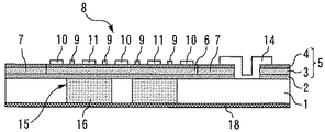
図1は、本発明の実施の形態1に係る半導体装置を示す上面図である。図2は図1のI−IIに沿った断面図である。Si基板1は互いに対向する第1及び第2の主表面を持つ。AlNからなるバッファ層2がSi基板1の第1の主表面上の全面に均一に形成されている。バッファ層2上に、順に積層されたGaN層3とAlGaN層4を有するエピタキシャル結晶成長層5が形成されている。
FIG. 1 is a top view showing a semiconductor device according to
エピタキシャル結晶成長層5の一部に活性層領域6が形成され、活性層領域6の周りに絶縁領域7が絶縁注入などにより形成されている。トランジスタ8がエピタキシャル結晶成長層5に形成されている。具体的には、活性層領域6上に、ゲート電極9と、その両側に配置されたソース電極10とドレイン電極11とにより一対を成す電界効果トランジスタが並列に並んでいる。これら活性層領域6と3つの電極が並列に並んだ領域にて動作領域を形成している。この動作領域を挟み対局する位置に1つ以上のゲートパッド12と1つ以上のドレインパッド13が配置されている。
An
動作領域内の全てのゲート電極9は、動作領域の外側で一つにまとめられ、ゲートパッド12に接続され、同様に動作領域内の全てのドレイン電極11は、動作領域の外側で一つにまとめられ、ドレインパッド13に接続される。また、ソース電極10は、通常ゲートパッド12の横に設けられたソースパッド14に接続される。ソース電極10とソースパッド14を接続する配線電極は、ゲート電極9を束ねている配線電極上に絶縁膜及び空気を介して配置されている。
All the
Si基板1の第2の主表面からバッファ層2に達する貫通孔15が設けられている。この貫通孔15にAlNからなる充填材16が充填されている。なお、各層の上記の物質は一例に過ぎず、バッファ層2はAlxGa1−xN(0≦x≦1)、エピタキシャル結晶成長層5はAlyGa1−yN(0≦y≦1,x≠y)、充填材16はバッファ層2と同じ組成比xのAlxGa1−xNからなる。
A through
続いて、上記の半導体装置の製造方法を説明する。まず、Si基板1の第1の主表面上にAlNのバッファ層2を形成する。次に、バッファ層2の上にエピタキシャル結晶成長層5を形成する。次に、エピタキシャル結晶成長層5にトランジスタ8を形成する。次に、Si基板1の第2の主面において、活性層領域6の下方以外の領域をレジストでマスキングした後、バッファ層2をストッパー層として用いて、第2の主表面から活性層領域6の下のSi基板1の一部をSF6などのフッ素系ガスによりドライエッチングして貫通孔15を形成する。次に、スパッタ又はCVDを用いて、貫通孔15にAlNの充填材16を充填する。
Next, a method for manufacturing the semiconductor device will be described. First, an
本実施の形態では、Si基板1の一部を除去して、Siよりも絶縁性が高く、かつ熱伝導率が高いAlxGa1−xNからなる充填材16で充填する。これにより、回路部の導体損失を低減し、トランジスタ下部における浮遊容量(Cdsなど)の増大を抑制して高周波特性を向上させることができる。また、トランジスタ8内部から発生する熱を充填材16を介して効率よくパッケージの金属ベースへと放熱させることができるため、信頼性の低下を防ぐことができる。
In the present embodiment, a part of the
また、充填材16はバッファ層2と同じ組成比xのAlxGa1−xNからなる。従って、バッファ層2と充填材16が格子整合しているため、充填材16の堆積が容易である。
The
また、従来装置では、高周波特性を少しでもよくするために、抵抗率が102〜104Ωcmの高抵抗Si基板を用いていた。しかし、本実施の形態では、トランジスタ下部及び回路部、配線部の下は、絶縁性が高い材料で充填されているため、それ以外の部分でSi基板1の抵抗率が低くても、半導体装置の高周波特性には影響を与えない。そこで、Si基板1の抵抗率を104Ωcm以下としても、半絶縁性基板並みの優れた高周波特性を得ることができる。
In the conventional apparatus, a high-resistance Si substrate having a resistivity of 10 2 to 10 4 Ωcm is used in order to improve the high-frequency characteristics as much as possible. However, in this embodiment, the lower portion of the transistor, the circuit portion, and the lower portion of the wiring portion are filled with a highly insulating material. It does not affect the high-frequency characteristics. Therefore, even if the resistivity of the
通常、高出力用の増幅器として用いられる半導体装置においては、高出力を得るために動作電圧を10V以上の高電圧状態で動作させることが多い。そこで、p型のSi基板1を用いてもよい。これにより、高電界がかかるゲート・ドレイン間にて発生したホールをソース電極10の下のp型のSi基板1から短距離にて裏面に引き抜くことができる。よって、高電界印加時にトランジスタ内部で生じたホールが、特にゲート電極9下のエピタキシャル結晶成長層内に溜まるのを抑制できる。この結果、活性層領域6にて均一に信頼性の向上を図ることができる。
Usually, a semiconductor device used as a high output amplifier is often operated in a high voltage state of 10 V or higher in order to obtain a high output. Therefore, a p-
また、窒化物のバッファ層2をストッパー層として用いてSi基板1をエッチングすることで、貫通孔15の形成が容易になる。
Further, the etching of the
実施の形態2.
図3は、本発明の実施の形態2に係る半導体装置を示す断面図である。本実施の形態では、貫通孔15及び充填材16は、ソース電極10の下方には設けられておらず、トランジスタ8のドレイン電極11の下方に設けられている。
FIG. 3 is a sectional view showing a semiconductor device according to the second embodiment of the present invention. In the present embodiment, the through
高周波特性の劣化の原因となるのは、ドレイン電極11と基板裏面との間の容量Cdsの増大であるため、ドレイン電極11においてSi基板1の一部を除去して充填材16で置き換えればよい。これにより、実施の形態1と同様に高周波特性を向上することができる。さらに、充填材16として堆積するAlN層の厚みは実施の形態1では数μm程度であるが、本実施の形態では更に薄くすることができるため、充填材16の形成が容易である。
The cause of the deterioration of the high frequency characteristics is an increase in the capacitance Cds between the
実施の形態3.
図4は、本発明の実施の形態3に係る半導体装置を示す断面図である。Si基板1の第2の主表面からトランジスタ8のソースパッド14に達するソースバイアホール17が絶縁領域7に設けられている。Auメッキなどの金属膜18が、ソースバイアホール17の内壁とSi基板1の第2の主表面に設けられ、ソースパッド14に接続されている。金属膜18により接地点までの距離を減らすことができるため、ソースインダクタンスを低減し、高周波特性を向上させることができる。
Embodiment 3 FIG.
FIG. 4 is a cross-sectional view showing a semiconductor device according to Embodiment 3 of the present invention. A source via
実施の形態4.
図5は、本発明の実施の形態4に係る半導体装置を示す断面図である。充填材16を充填する際に、まず充填材16をSi基板1の第2の主面上及び貫通孔15内に形成する。次に、Si基板1の第2の主表面に形成された充填材16を研削又はCMPなどを用いて削って平坦化する。ドレイン電極11下のみ充填材16を埋めこんだ状態でソースバイアホール17を形成する。基板裏面の余分なAlNを削り取ることでフラットな裏面を形成できるため、アセンブリ性に優れた半導体装置を得ることができる。
Embodiment 4 FIG.
FIG. 5 is a cross-sectional view showing a semiconductor device according to Embodiment 4 of the present invention. When filling the
実施の形態5.
図6は、本発明の実施の形態5に係る半導体装置を示す断面図である。n型のSi基板1を用いる。絶縁領域7内のソースパッド14の直下のバッファ層2及びエピタキシャル結晶成長層5に設けられた開口を介してソースパッド14がn型のSi基板1に直接コンタクトしている。これにより、表面のソースパッド14はn型のSi基板1を介して基板裏面の金属膜18と接続されるため、ソースバイアホール17が不要となる。よって、実施の形態4と同様の効果を得つつ、半導体装置作製工程を簡略化することができる。
FIG. 6 is a sectional view showing a semiconductor device according to the fifth embodiment of the present invention. An n-
実施の形態6.
図7は、本発明の実施の形態6に係る半導体装置を示す断面図である。n型のSi基板1を用いる。活性層領域6内の各ソース電極10の直下のバッファ層2及びエピタキシャル結晶成長層5に設けられた開口を介してソース電極10がn型のSi基板1に直接コンタクトしている。これにより、表面のソース電極10はn型のSi基板1を介して基板裏面の金属膜18と接続されるため、絶縁領域7のソースパッド14が不要となり、チップパターンを縮小化できる。また、各ソース電極10から最短距離にて金属膜18までの導通が図れる。これにより、配線ロス、インダクタンスを低減することができ、更に高周波特性を向上させることができる。
FIG. 7 is a sectional view showing a semiconductor device according to the sixth embodiment of the present invention. An n-
実施の形態7.
図8は、本発明の実施の形態7に係る半導体装置を示す断面図である。実施の形態1のAlNからなる充填材16の代わりに、貫通孔15内に1層目にダイヤモンド薄膜19、2層目にAlN又はCuの充填材20を充填する。ダイヤモンドは半導体の中でも優れた絶縁性と熱伝導性を持つ。このため、高周波特性を更に向上させ、かつトランジスタ8内部から発生する熱を効率よく放熱させることができる。なお、ダイヤモンドだけで貫通孔15を埋め込むと費用がかかるので、2層目にAlN又はCuの充填材20を堆積させている。
FIG. 8 is a sectional view showing a semiconductor device according to the seventh embodiment of the present invention. Instead of the
1 Si基板、2 バッファ層、5 エピタキシャル結晶成長層、8 トランジスタ、10 ソース電極、11 ドレイン電極、14 ソースパッド、15 貫通孔、16,20 充填材、17 ソースバイアホール、18 金属膜、19 ダイヤモンド薄膜 1 Si substrate, 2 buffer layer, 5 epitaxial crystal growth layer, 8 transistor, 10 source electrode, 11 drain electrode, 14 source pad, 15 through hole, 16, 20 filler, 17 source via hole, 18 metal film, 19 diamond Thin film
Claims (9)
前記Si基板の前記第1の主表面上に形成され、AlxGa1−xN(0≦x≦1)からなるバッファ層と、
前記バッファ層の上に形成され、AlyGa1−yN(0≦y≦1,x≠y)からなるエピタキシャル結晶成長層と、
前記エピタキシャル結晶成長層に形成されたトランジスタと、
前記Si基板の前記第2の主表面から前記バッファ層に達する貫通孔に充填され、前記バッファ層と同じ組成比xのAlxGa1−xNからなる充填材とを備え、
前記貫通孔及び前記充填材は、前記トランジスタのソース電極の下方には設けられておらず、前記トランジスタのゲート電極及びドレイン電極の下方に設けられていることを特徴とする半導体装置。 Si substrates having first and second main surfaces facing each other;
A buffer layer formed on the first main surface of the Si substrate and made of Al x Ga 1-x N (0 ≦ x ≦ 1);
An epitaxial crystal growth layer formed on the buffer layer and made of Al y Ga 1-y N (0 ≦ y ≦ 1, x ≠ y);
A transistor formed in the epitaxial crystal growth layer;
Filling a through hole reaching the buffer layer from the second main surface of the Si substrate, and comprising a filler made of Al x Ga 1-x N having the same composition ratio x as the buffer layer ,
The semiconductor device is characterized in that the through hole and the filler are not provided below the source electrode of the transistor, but are provided below the gate electrode and the drain electrode of the transistor .
前記バッファ層の上に、AlyGa1−yN(0≦y≦1,x≠y)からなるエピタキシャル結晶成長層を形成する工程と、
前記エピタキシャル結晶成長層にトランジスタを形成する工程と、
前記バッファ層をストッパー層として用いて、前記第2の主表面から前記Si基板をエッチングして貫通孔を形成する工程と、
前記貫通孔に前記バッファ層と同じ組成比xのAlxGa1−xNからなる充填材を充填する工程とを備え、
前記貫通孔及び前記充填材を、前記トランジスタのソース電極の下方には設けず、前記トランジスタのゲート電極及びドレイン電極の下方に設けることを特徴とする半導体装置の製造方法。 Forming a buffer layer made of Al x Ga 1-x N (0 ≦ x ≦ 1) on the first main surface of the Si substrate having first and second main surfaces facing each other;
Forming an epitaxial crystal growth layer made of Al y Ga 1-y N (0 ≦ y ≦ 1, x ≠ y) on the buffer layer;
Forming a transistor in the epitaxial crystal growth layer;
Etching the Si substrate from the second main surface to form a through hole using the buffer layer as a stopper layer;
Filling the through hole with a filler made of Al x Ga 1-x N having the same composition ratio x as the buffer layer ,
The method of manufacturing a semiconductor device, wherein the through hole and the filler are not provided below the source electrode of the transistor but below the gate electrode and the drain electrode of the transistor .
前記充填材を前記Si基板の前記第2の主面上及び前記貫通孔内に形成する工程と、
前記Si基板の前記第2の主面上に形成された前記充填材を削って平坦化する工程とを有することを特徴とする請求項7に記載の半導体装置の製造方法。 The step of filling the filler comprises
Forming the filler on the second main surface of the Si substrate and in the through hole;
The method for manufacturing a semiconductor device according to claim 7 , further comprising a step of cutting and planarizing the filler formed on the second main surface of the Si substrate.
Priority Applications (5)
| Application Number | Priority Date | Filing Date | Title |
|---|---|---|---|
| JP2013197261A JP6156015B2 (en) | 2013-09-24 | 2013-09-24 | Semiconductor device and manufacturing method thereof |
| US14/295,532 US9117896B2 (en) | 2013-09-24 | 2014-06-04 | Semiconductor device with improved conductivity |
| DE102014213565.6A DE102014213565B4 (en) | 2013-09-24 | 2014-07-11 | Semiconductor device and method of manufacturing the same |
| KR1020140118362A KR101561519B1 (en) | 2013-09-24 | 2014-09-05 | Semiconductor device and method for manufacturing the same |
| CN201410489794.2A CN104465770A (en) | 2013-09-24 | 2014-09-23 | Semiconductor Device And Method For Manufacturing The Same |
Applications Claiming Priority (1)
| Application Number | Priority Date | Filing Date | Title |
|---|---|---|---|
| JP2013197261A JP6156015B2 (en) | 2013-09-24 | 2013-09-24 | Semiconductor device and manufacturing method thereof |
Publications (3)
| Publication Number | Publication Date |
|---|---|
| JP2015065233A JP2015065233A (en) | 2015-04-09 |
| JP2015065233A5 JP2015065233A5 (en) | 2016-09-01 |
| JP6156015B2 true JP6156015B2 (en) | 2017-07-05 |
Family
ID=52623790
Family Applications (1)
| Application Number | Title | Priority Date | Filing Date |
|---|---|---|---|
| JP2013197261A Active JP6156015B2 (en) | 2013-09-24 | 2013-09-24 | Semiconductor device and manufacturing method thereof |
Country Status (5)
| Country | Link |
|---|---|
| US (1) | US9117896B2 (en) |
| JP (1) | JP6156015B2 (en) |
| KR (1) | KR101561519B1 (en) |
| CN (1) | CN104465770A (en) |
| DE (1) | DE102014213565B4 (en) |
Families Citing this family (20)
| Publication number | Priority date | Publication date | Assignee | Title |
|---|---|---|---|---|
| DE102016200825A1 (en) * | 2016-01-21 | 2017-07-27 | Robert Bosch Gmbh | Apparatus and method for producing a lateral HEMT |
| US10128364B2 (en) * | 2016-03-28 | 2018-11-13 | Nxp Usa, Inc. | Semiconductor devices with an enhanced resistivity region and methods of fabrication therefor |
| WO2017171870A1 (en) * | 2016-04-01 | 2017-10-05 | Intel Corporation | Gallium nitride transistor with underfill aluminum nitride for improved thermal and rf performance |
| US11676880B2 (en) | 2016-11-26 | 2023-06-13 | Texas Instruments Incorporated | High thermal conductivity vias by additive processing |
| US10529641B2 (en) | 2016-11-26 | 2020-01-07 | Texas Instruments Incorporated | Integrated circuit nanoparticle thermal routing structure over interconnect region |
| US10861763B2 (en) | 2016-11-26 | 2020-12-08 | Texas Instruments Incorporated | Thermal routing trench by additive processing |
| US11004680B2 (en) | 2016-11-26 | 2021-05-11 | Texas Instruments Incorporated | Semiconductor device package thermal conduit |
| US10811334B2 (en) | 2016-11-26 | 2020-10-20 | Texas Instruments Incorporated | Integrated circuit nanoparticle thermal routing structure in interconnect region |
| US10256188B2 (en) | 2016-11-26 | 2019-04-09 | Texas Instruments Incorporated | Interconnect via with grown graphitic material |
| CN106783993B (en) * | 2017-01-18 | 2019-08-02 | 电子科技大学 | Gallium nitride heterojunction field-effect tube with compound medium layer structure in substrate |
| KR102351759B1 (en) * | 2017-09-01 | 2022-01-14 | 미쓰비시덴키 가부시키가이샤 | field effect transistor |
| KR102327745B1 (en) | 2018-02-01 | 2021-11-17 | 미쓰비시덴키 가부시키가이샤 | Semiconductor device and manufacturing method thereof |
| JP7137947B2 (en) * | 2018-03-22 | 2022-09-15 | ローム株式会社 | Nitride semiconductor device |
| US11158575B2 (en) * | 2018-06-05 | 2021-10-26 | Macom Technology Solutions Holdings, Inc. | Parasitic capacitance reduction in GaN-on-silicon devices |
| GB2589484B (en) * | 2018-06-28 | 2022-09-28 | Mitsubishi Electric Corp | Semiconductor device and method of manufacturing semiconductor device |
| JP7248410B2 (en) * | 2018-11-01 | 2023-03-29 | エア・ウォーター株式会社 | Compound semiconductor device, compound semiconductor substrate, and method for manufacturing compound semiconductor device |
| WO2020203506A1 (en) * | 2019-04-01 | 2020-10-08 | パナソニックセミコンダクターソリューションズ株式会社 | Power amplication device |
| WO2020255259A1 (en) * | 2019-06-18 | 2020-12-24 | 三菱電機株式会社 | Semiconductor device and method for producing same |
| EP4283667A4 (en) * | 2021-02-26 | 2024-04-10 | Huawei Tech Co Ltd | Semiconductor device, electronic apparatus, and preparation method for semiconductor device |
| US20230420326A1 (en) * | 2022-06-22 | 2023-12-28 | Globalfoundries U.S. Inc. | High-mobility-electron transistors having heat dissipating structures |
Family Cites Families (10)
| Publication number | Priority date | Publication date | Assignee | Title |
|---|---|---|---|---|
| JP2001274174A (en) * | 2000-03-27 | 2001-10-05 | Toshiba Corp | High-frequency semiconductor device |
| JP2005243727A (en) | 2004-02-24 | 2005-09-08 | Mitsubishi Electric Corp | Semiconductor device and its manufacturing method |
| JP5383059B2 (en) | 2008-02-26 | 2014-01-08 | ローム株式会社 | Field effect transistor |
| JP5396784B2 (en) | 2008-09-09 | 2014-01-22 | 日本電気株式会社 | Semiconductor device and manufacturing method thereof |
| JP5487590B2 (en) * | 2008-10-20 | 2014-05-07 | 富士通株式会社 | Semiconductor device and manufacturing method thereof |
| JP2011060912A (en) * | 2009-09-08 | 2011-03-24 | Toshiba Corp | Semiconductor device |
| JP5707786B2 (en) * | 2010-08-31 | 2015-04-30 | 富士通株式会社 | Compound semiconductor device and manufacturing method thereof |
| US8835986B2 (en) * | 2011-06-22 | 2014-09-16 | Imec | Method for fabrication of III-nitride device and the III-nitride device thereof |
| JP5629714B2 (en) | 2012-03-19 | 2014-11-26 | トヨタ自動車株式会社 | Semiconductor device |
| KR101922123B1 (en) * | 2012-09-28 | 2018-11-26 | 삼성전자주식회사 | Semiconductor device and method of manufacturing the same |
-
2013
- 2013-09-24 JP JP2013197261A patent/JP6156015B2/en active Active
-
2014
- 2014-06-04 US US14/295,532 patent/US9117896B2/en active Active
- 2014-07-11 DE DE102014213565.6A patent/DE102014213565B4/en active Active
- 2014-09-05 KR KR1020140118362A patent/KR101561519B1/en active IP Right Grant
- 2014-09-23 CN CN201410489794.2A patent/CN104465770A/en active Pending
Also Published As
| Publication number | Publication date |
|---|---|
| KR20150033538A (en) | 2015-04-01 |
| CN104465770A (en) | 2015-03-25 |
| DE102014213565A1 (en) | 2015-03-26 |
| KR101561519B1 (en) | 2015-10-19 |
| DE102014213565B4 (en) | 2021-02-04 |
| JP2015065233A (en) | 2015-04-09 |
| US9117896B2 (en) | 2015-08-25 |
| US20150084103A1 (en) | 2015-03-26 |
Similar Documents
| Publication | Publication Date | Title |
|---|---|---|
| JP6156015B2 (en) | Semiconductor device and manufacturing method thereof | |
| TWI517383B (en) | Direct growth of diamond in backside vias for gan hemt devices | |
| JP6268366B2 (en) | Semiconductor device | |
| CN106910724B (en) | Semiconductor device with a plurality of transistors | |
| US8026596B2 (en) | Thermal designs of packaged gallium nitride material devices and methods of packaging | |
| JP6367533B2 (en) | Normally-off high electron mobility transistor | |
| US9536965B2 (en) | Heat spreader on GaN semiconductor device | |
| WO2012017588A1 (en) | Semiconductor device and method for manufacturing same | |
| US8916962B2 (en) | III-nitride transistor with source-connected heat spreading plate | |
| JP2016171197A (en) | Semiconductor device | |
| JP2010067662A (en) | Semiconductor device and manufacturing method for the same | |
| JP6834546B2 (en) | Semiconductor devices and their manufacturing methods | |
| JP2018041785A (en) | Semiconductor device and fabrication method of semiconductor device | |
| JP6249146B1 (en) | Semiconductor device | |
| US20150021666A1 (en) | Transistor having partially or wholly replaced substrate and method of making the same | |
| KR20140115585A (en) | Multiple field plate transistor and manufacturing method thereof | |
| JP2012164900A (en) | Compound semiconductor device, and method of manufacturing compound semiconductor device | |
| JP2010165789A (en) | Semiconductor integrated circuit and method of manufacturing the same | |
| KR101985897B1 (en) | Method of manufacturing high-electron-mobility transistor with high linearlity and high power | |
| WO2017098603A1 (en) | Nitride semiconductor device | |
| US11728419B2 (en) | High electron mobility transistor | |
| KR101004332B1 (en) | Transistor having heat dissipation structure | |
| KR101015787B1 (en) | Transistor having heat dissipation structure | |
| CN113906571B (en) | Semiconductor device and method for manufacturing the same | |
| JP2011192882A (en) | Semiconductor structure, semiconductor device, and method of manufacturing the same |
Legal Events
| Date | Code | Title | Description |
|---|---|---|---|
| A521 | Request for written amendment filed |
Free format text: JAPANESE INTERMEDIATE CODE: A523 Effective date: 20160713 |
|
| A621 | Written request for application examination |
Free format text: JAPANESE INTERMEDIATE CODE: A621 Effective date: 20160713 |
|
| A131 | Notification of reasons for refusal |
Free format text: JAPANESE INTERMEDIATE CODE: A131 Effective date: 20170221 |
|
| A977 | Report on retrieval |
Free format text: JAPANESE INTERMEDIATE CODE: A971007 Effective date: 20170223 |
|
| A521 | Request for written amendment filed |
Free format text: JAPANESE INTERMEDIATE CODE: A523 Effective date: 20170314 |
|
| TRDD | Decision of grant or rejection written | ||
| A01 | Written decision to grant a patent or to grant a registration (utility model) |
Free format text: JAPANESE INTERMEDIATE CODE: A01 Effective date: 20170509 |
|
| A61 | First payment of annual fees (during grant procedure) |
Free format text: JAPANESE INTERMEDIATE CODE: A61 Effective date: 20170522 |
|
| R150 | Certificate of patent or registration of utility model |
Ref document number: 6156015 Country of ref document: JP Free format text: JAPANESE INTERMEDIATE CODE: R150 |
|
| R250 | Receipt of annual fees |
Free format text: JAPANESE INTERMEDIATE CODE: R250 |
|
| R250 | Receipt of annual fees |
Free format text: JAPANESE INTERMEDIATE CODE: R250 |
|
| R250 | Receipt of annual fees |
Free format text: JAPANESE INTERMEDIATE CODE: R250 |
|
| R250 | Receipt of annual fees |
Free format text: JAPANESE INTERMEDIATE CODE: R250 |