EP3224631B1 - Method for determining the ageing of power semiconductor modules and device and circuit assembly - Google Patents
Method for determining the ageing of power semiconductor modules and device and circuit assembly Download PDFInfo
- Publication number
- EP3224631B1 EP3224631B1 EP15821054.2A EP15821054A EP3224631B1 EP 3224631 B1 EP3224631 B1 EP 3224631B1 EP 15821054 A EP15821054 A EP 15821054A EP 3224631 B1 EP3224631 B1 EP 3224631B1
- Authority
- EP
- European Patent Office
- Prior art keywords
- power semiconductor
- semiconductor module
- temperature
- tsep
- electrical parameter
- Prior art date
- Legal status (The legal status is an assumption and is not a legal conclusion. Google has not performed a legal analysis and makes no representation as to the accuracy of the status listed.)
- Active
Links
- 239000004065 semiconductor Substances 0.000 title claims description 256
- 238000000034 method Methods 0.000 title claims description 22
- 230000032683 aging Effects 0.000 title description 29
- 238000005259 measurement Methods 0.000 claims description 9
- 238000001816 cooling Methods 0.000 claims description 4
- 238000010438 heat treatment Methods 0.000 claims description 3
- 230000006866 deterioration Effects 0.000 claims 2
- 238000009532 heart rate measurement Methods 0.000 claims 1
- 229910000679 solder Inorganic materials 0.000 description 7
- 238000012544 monitoring process Methods 0.000 description 6
- 230000001419 dependent effect Effects 0.000 description 5
- 230000002441 reversible effect Effects 0.000 description 4
- 238000010586 diagram Methods 0.000 description 3
- 230000002028 premature Effects 0.000 description 3
- 230000000750 progressive effect Effects 0.000 description 3
- 238000005382 thermal cycling Methods 0.000 description 3
- 239000003990 capacitor Substances 0.000 description 2
- 238000001514 detection method Methods 0.000 description 2
- 239000000758 substrate Substances 0.000 description 2
- 238000012360 testing method Methods 0.000 description 2
- 230000000930 thermomechanical effect Effects 0.000 description 2
- 238000005050 thermomechanical fatigue Methods 0.000 description 2
- 238000012546 transfer Methods 0.000 description 2
- 238000011161 development Methods 0.000 description 1
- 230000018109 developmental process Effects 0.000 description 1
- 238000002474 experimental method Methods 0.000 description 1
- 230000005669 field effect Effects 0.000 description 1
- 239000004519 grease Substances 0.000 description 1
- 230000007257 malfunction Effects 0.000 description 1
- 239000000463 material Substances 0.000 description 1
- 229910044991 metal oxide Inorganic materials 0.000 description 1
- 150000004706 metal oxides Chemical class 0.000 description 1
- 230000003071 parasitic effect Effects 0.000 description 1
- 238000011084 recovery Methods 0.000 description 1
- 238000004904 shortening Methods 0.000 description 1
- 230000035882 stress Effects 0.000 description 1
- 230000001052 transient effect Effects 0.000 description 1
Images

Classifications
-
- G—PHYSICS
- G01—MEASURING; TESTING
- G01R—MEASURING ELECTRIC VARIABLES; MEASURING MAGNETIC VARIABLES
- G01R31/00—Arrangements for testing electric properties; Arrangements for locating electric faults; Arrangements for electrical testing characterised by what is being tested not provided for elsewhere
- G01R31/26—Testing of individual semiconductor devices
- G01R31/2607—Circuits therefor
- G01R31/2608—Circuits therefor for testing bipolar transistors
- G01R31/2619—Circuits therefor for testing bipolar transistors for measuring thermal properties thereof
-
- G—PHYSICS
- G01—MEASURING; TESTING
- G01K—MEASURING TEMPERATURE; MEASURING QUANTITY OF HEAT; THERMALLY-SENSITIVE ELEMENTS NOT OTHERWISE PROVIDED FOR
- G01K7/00—Measuring temperature based on the use of electric or magnetic elements directly sensitive to heat ; Power supply therefor, e.g. using thermoelectric elements
- G01K7/01—Measuring temperature based on the use of electric or magnetic elements directly sensitive to heat ; Power supply therefor, e.g. using thermoelectric elements using semiconducting elements having PN junctions
-
- G—PHYSICS
- G01—MEASURING; TESTING
- G01K—MEASURING TEMPERATURE; MEASURING QUANTITY OF HEAT; THERMALLY-SENSITIVE ELEMENTS NOT OTHERWISE PROVIDED FOR
- G01K7/00—Measuring temperature based on the use of electric or magnetic elements directly sensitive to heat ; Power supply therefor, e.g. using thermoelectric elements
- G01K7/42—Circuits effecting compensation of thermal inertia; Circuits for predicting the stationary value of a temperature
-
- G—PHYSICS
- G01—MEASURING; TESTING
- G01R—MEASURING ELECTRIC VARIABLES; MEASURING MAGNETIC VARIABLES
- G01R31/00—Arrangements for testing electric properties; Arrangements for locating electric faults; Arrangements for electrical testing characterised by what is being tested not provided for elsewhere
- G01R31/26—Testing of individual semiconductor devices
- G01R31/2607—Circuits therefor
- G01R31/2608—Circuits therefor for testing bipolar transistors
- G01R31/261—Circuits therefor for testing bipolar transistors for measuring break-down voltage or punch through voltage therefor
-
- G—PHYSICS
- G01—MEASURING; TESTING
- G01R—MEASURING ELECTRIC VARIABLES; MEASURING MAGNETIC VARIABLES
- G01R31/00—Arrangements for testing electric properties; Arrangements for locating electric faults; Arrangements for electrical testing characterised by what is being tested not provided for elsewhere
- G01R31/26—Testing of individual semiconductor devices
- G01R31/2607—Circuits therefor
- G01R31/2608—Circuits therefor for testing bipolar transistors
- G01R31/2612—Circuits therefor for testing bipolar transistors for measuring frequency response characteristics, e.g. cut-off frequency thereof
-
- G—PHYSICS
- G01—MEASURING; TESTING
- G01R—MEASURING ELECTRIC VARIABLES; MEASURING MAGNETIC VARIABLES
- G01R31/00—Arrangements for testing electric properties; Arrangements for locating electric faults; Arrangements for electrical testing characterised by what is being tested not provided for elsewhere
- G01R31/26—Testing of individual semiconductor devices
- G01R31/2607—Circuits therefor
- G01R31/2608—Circuits therefor for testing bipolar transistors
- G01R31/2614—Circuits therefor for testing bipolar transistors for measuring gain factor thereof
-
- G—PHYSICS
- G01—MEASURING; TESTING
- G01R—MEASURING ELECTRIC VARIABLES; MEASURING MAGNETIC VARIABLES
- G01R31/00—Arrangements for testing electric properties; Arrangements for locating electric faults; Arrangements for electrical testing characterised by what is being tested not provided for elsewhere
- G01R31/26—Testing of individual semiconductor devices
- G01R31/2607—Circuits therefor
- G01R31/2621—Circuits therefor for testing field effect transistors, i.e. FET's
- G01R31/2628—Circuits therefor for testing field effect transistors, i.e. FET's for measuring thermal properties thereof
-
- G—PHYSICS
- G01—MEASURING; TESTING
- G01R—MEASURING ELECTRIC VARIABLES; MEASURING MAGNETIC VARIABLES
- G01R31/00—Arrangements for testing electric properties; Arrangements for locating electric faults; Arrangements for electrical testing characterised by what is being tested not provided for elsewhere
- G01R31/26—Testing of individual semiconductor devices
- G01R31/2642—Testing semiconductor operation lifetime or reliability, e.g. by accelerated life tests
-
- G—PHYSICS
- G01—MEASURING; TESTING
- G01K—MEASURING TEMPERATURE; MEASURING QUANTITY OF HEAT; THERMALLY-SENSITIVE ELEMENTS NOT OTHERWISE PROVIDED FOR
- G01K3/00—Thermometers giving results other than momentary value of temperature
- G01K3/08—Thermometers giving results other than momentary value of temperature giving differences of values; giving differentiated values
- G01K3/10—Thermometers giving results other than momentary value of temperature giving differences of values; giving differentiated values in respect of time, e.g. reacting only to a quick change of temperature
-
- G—PHYSICS
- G01—MEASURING; TESTING
- G01R—MEASURING ELECTRIC VARIABLES; MEASURING MAGNETIC VARIABLES
- G01R31/00—Arrangements for testing electric properties; Arrangements for locating electric faults; Arrangements for electrical testing characterised by what is being tested not provided for elsewhere
- G01R31/50—Testing of electric apparatus, lines, cables or components for short-circuits, continuity, leakage current or incorrect line connections
- G01R31/66—Testing of connections, e.g. of plugs or non-disconnectable joints
- G01R31/70—Testing of connections between components and printed circuit boards
-
- H—ELECTRICITY
- H02—GENERATION; CONVERSION OR DISTRIBUTION OF ELECTRIC POWER
- H02M—APPARATUS FOR CONVERSION BETWEEN AC AND AC, BETWEEN AC AND DC, OR BETWEEN DC AND DC, AND FOR USE WITH MAINS OR SIMILAR POWER SUPPLY SYSTEMS; CONVERSION OF DC OR AC INPUT POWER INTO SURGE OUTPUT POWER; CONTROL OR REGULATION THEREOF
- H02M1/00—Details of apparatus for conversion
- H02M1/32—Means for protecting converters other than automatic disconnection
- H02M1/327—Means for protecting converters other than automatic disconnection against abnormal temperatures
-
- H—ELECTRICITY
- H03—ELECTRONIC CIRCUITRY
- H03K—PULSE TECHNIQUE
- H03K17/00—Electronic switching or gating, i.e. not by contact-making and –breaking
- H03K17/08—Modifications for protecting switching circuit against overcurrent or overvoltage
- H03K2017/0806—Modifications for protecting switching circuit against overcurrent or overvoltage against excessive temperature
Definitions
- the invention relates to a method for characterizing a power semiconductor module having at least one power semiconductor component.
- the invention also relates to a device and a circuit arrangement.
- Power semiconductor modules are already known from the prior art and may include, for example, an inverter or a converter.
- Power semiconductor modules generally comprise at least one power semiconductor chip or a power semiconductor component, which is designed in particular for controlling and switching high electrical currents and voltages.
- a power semiconductor device may be, for example, a power metal oxide field effect transistor (power MOSFET), a power diode or an insulated gate bipolar transistor (IGBT).
- the power semiconductor components are usually soldered onto a substrate to form the power semiconductor module and electrically connected to one another by bond connections.
- Power semiconductor modules can be characterized over their lifetime.
- the life of the power semiconductor module is a time to failure or a malfunction of the power semiconductor module.
- a remaining service life of the power semiconductor module a so-called remaining service life of the power semiconductor module, may change, for example as a result of aging of the power semiconductor module. It is especially true that the remaining life of the power semiconductor module shortens the faster the power module ages.
- the aging of the power semiconductor module is usually accelerated during operation, in which the power semiconductor modules can be exposed to thermal and mechanical stresses. These thermal and mechanical loads of the power semiconductor modules can lead to a so-called thermo-mechanical fatigue of the power semiconductor module, which can result in the failure or inoperability of the power semiconductor module and thus an end to the life.
- Thermal loads can be, for example, thermal cycling due to the electrical operation of the power semiconductor module, which, in particular due to different thermal expansion coefficients of the materials in the power semiconductor module to fatigue of the electrical connection points, such as bonds and solder joints of the chip solder and the system solder lead. Due to the fatigue of the connection points, for example, the bond connections or the solder joints may become loose, which leads to an increased temperature of the semiconductor chip. Overall, therefore, the aging of the power semiconductor module is accelerated by the thermo-mechanical fatigue of the power semiconductor module, which can lead to a reduced residual life and to a premature failure of the power semiconductor module.
- lifetime calculations of lifetime curves of the power semiconductor modules are performed on the basis of lifetime curves and predetermined load profiles in a computer-aided manner.
- a temperature of the power semiconductor modules is monitored by, for example, thermistors being soldered together with the power semiconductor components to the substrate.
- thermistors being soldered together with the power semiconductor components to the substrate.
- the exact transient temperatures of the chips can not be accurately detected, whereby no accurate lifetime calculations can be performed.
- thermal equivalent circuit diagrams for the power semiconductor modules on the basis of which the temperature of the power semiconductor components can be indirectly deduced.
- Current and voltage measurements or the knowledge of the operating point of the power semiconductor module, the electrical losses of the IGBTs and the diodes can be calculated.
- the temperatures of the power semiconductor devices can be calculated during operation, but in the thermal equivalent circuit diagrams usually no aging of the power semiconductor devices is taken into account.
- a characteristic of a gate-emitter voltage is determined and from this during a switch-off phase pulses are determined which describe a start and an end of a Millerplateaus. Based on a time delay between the start and the end of the junction temperature and / or the remaining life can then be calculated.
- the temperature-dependent impedance is determined on the basis of a warm-up curve recorded during operation of the power semiconductor.
- a method according to the invention serves to characterize a power semiconductor module having at least one power semiconductor component.
- a thermal model of the power semiconductor module is determined at a reference time, which is before startup of the power semiconductor module, wherein a thermal impedance of the power semiconductor module describing a thermal path of the power semiconductor module is determined to create the thermal model.
- a reference temperature based on the thermal model of the power semiconductor module determined, at least one temperature-sensitive electrical parameter (TSEP) of the power semiconductor module to at least one compared to the reference time later time measured during operation of the power semiconductor module, a current temperature of the power semiconductor module from the at least one measured temperature-sensitive electrical parameter of the power semiconductor module determines a temperature difference between the current temperature and the reference temperature is determined and determines an aging of the power semiconductor module based on the determined temperature difference.
- TSEP temperature-sensitive electrical parameter
- the power semiconductor module may comprise, for example, an inverter or a converter and preferably has an IGBT as the at least one power semiconductor component.
- the aging or an aging progress of the power semiconductor module is determined.
- the thermal semiconductor module characterizing the power semiconductor module at the reference time is determined for the power semiconductor module.
- the thermal model is used to describe the thermal behavior of the power semiconductor module.
- heat sources or heat sinks within the power semiconductor module are taken into account in the thermal model. Such heat sources are preferably calculated via a power loss of the power semiconductor module, which can be determined by means of current and voltage measurements.
- the power semiconductor module has a non-aged state, which is also referred to as a healthy state of the power semiconductor module, in which the power semiconductor module in particular shows no signs of wear or wear.
- This reference time is before commissioning of the power semiconductor module. This means that the power semiconductor module does not yet have thermomechanical loads, which was usually the fatigue or accelerated aging of the power semiconductor module, was exposed.
- This thermal model created at the reference time thus represents an initial state of the power semiconductor module.
- the reference temperature of the power semiconductor module which corresponds to a so-called junction temperature, is determined.
- This reference temperature characterizes the unaged state or the healthy state of the power semiconductor module.
- the reference temperature can be calculated directly from the known relationships between power loss and temperature.
- At least one temperature-sensitive electrical parameter of the power semiconductor module during operation of the power semiconductor module is measured at the later time, which is later than the reference time.
- the power semiconductor module is exposed to thermo-mechanical loads, which may cause the power semiconductor module to age. The measurement can be carried out continuously or at predetermined measuring times during operation of the power semiconductor module.
- a corresponding measuring circuit can be provided for measuring the at least one temperature-sensitive electrical parameter of the power semiconductor module.
- the power semiconductor module or the at least one power semiconductor element has an integrated measuring device, for example a diode, has, by means of which a temperature monitoring of the power semiconductor modules can be performed.
- a current temperature ie a temperature which has the power semiconductor module at the respective measurement time, determined or calculated. This current temperature is compared with the reference temperature and the temperature difference between the reference temperature and the current temperature is determined.
- the invention is based on the finding that during the aging of the power semiconductor module, for example due to wear, in particular by the already described release of bonding or solder joints, a temperature of the power semiconductor module changes in the healthy state compared to the reference temperature of the power semiconductor module.
- a temperature of the power semiconductor module changes in the healthy state compared to the reference temperature of the power semiconductor module.
- aging of the power semiconductor module can be estimated or determined. In an unaged condition, this temperature difference is about zero. As the aging progresses and the signs of wear increase, the temperature difference increases, with the relative change in the temperature difference providing an indication of an aging power semiconductor module.
- an aging of the power semiconductor module can be determined in a particularly simple manner by determining the temperature difference, and thus a remaining service life or availability of the semiconductor module can be predicted. Thereby a reliable operation of the power semiconductor module can be ensured in its respective field of application. Because the aging is determined during operation or during the operating phases of the power semiconductor module, an interruption of the operation of the power semiconductor module can be avoided in an advantageous manner.
- the method is therefore designed to be particularly user-friendly.
- a temperature-difference-dependent power control of the power semiconductor module can be provided to avoid increased operating temperatures and thermal cycling.
- a control device can be provided which, on the basis of the determined temperature difference, performs a corresponding power control for efficient operation of the power semiconductor module.
- a thermal impedance of the power semiconductor module describing a thermal path of the power semiconductor module is determined.
- the thermal impedance of the power semiconductor module is determined or measured at the reference time at which the power semiconductor module has the initial state or the unaged state.
- the thermal path of the power semiconductor module can be described or parameterized.
- the thermal impedance is a thermal characteristic and a measure of a temperature differential that arises in the power semiconductor module as a heat flow passes therethrough.
- the thermal impedance of the power semiconductor module is composed of the individual thermal impedances of the power semiconductor components.
- the thermal impedance can for example be calculated from a thermal equivalent circuit diagram.
- the characteristics describing the thermal behavior can be transferred into electrical quantities.
- electrical quantities an electrical network can be created, which can be calculated analytically or by means of a circuit simulator.
- a particularly accurate and reliable model of the power semiconductor module can be determined.
- a power loss or a heat output of the power semiconductor module is determined to create the thermal model.
- the heat output or the power loss is calculated in particular in the operating point of the power semiconductor module by measuring the output voltage and the output current of the power semiconductor module and by forming the product of output voltage and output current. Based on the determination of the heat output of the power semiconductor module, the thermal model can be created in a particularly simple manner.
- a temperature of a heat sink of the power semiconductor module is detected during operation of the power semiconductor module.
- a heat sink may for example be a cooling plate whose temperature is measured during operation of the power semiconductor module.
- the heat sink as a heat source or a heat sink can thus also be taken into account in the thermal model, whereby the thermal model is designed particularly accurate and reliable.
- At least one of the following variables is measured as the at least one temperature-sensitive electrical parameter of the power semiconductor module which preferably has an IGBT as the at least one power semiconductor component: an electrical threshold voltage, ie a gate-emitter voltage, a miller plateau, a switch-on delay time of the power semiconductor module, a switch-off delay time the power semiconductor module, a current rise speed, a reverse charge delay or a reverse recovery charge, a tail current, which characterizes the turn-off of the power semiconductor module, a voltage peak of the power semiconductor module during a power-on, a turn-on of the power semiconductor module or a turn-off of the power semiconductor module. Since each of these variables is temperature-dependent, a current temperature of the power semiconductor module can be determined in a particularly simple manner from the measured values of these variables.
- a characteristic curve for the power semiconductor module is determined on the basis of which each value of the at least one temperature-sensitive electrical parameter is assigned a temperature value, one of the temperature values being determined as the current temperature as a function of the measured temperature-sensitive electrical parameter.
- This characteristic is in particular determined once at a calibration time, for example in the healthy state of the power semiconductor module.
- values of the at least one temperature-sensitive electrical parameter are plotted against the temperature. At the later time, the temperature corresponding to the value of the temperature-sensitive electrical parameter measured during operation can be determined as the current temperature particularly quickly and without great computational effort on the basis of this predetermined characteristic curve.
- the characteristic curve is preferably determined by specifying the temperature values for the power semiconductor module, the power semiconductor module to the respective temperature value is tempered or adjusted and the respective value of the at least one temperature-sensitive electrical parameter at the predetermined temperature value is measured.
- a heating device is provided, by means of which the power semiconductor module can be heated to the respective predetermined temperature values.
- the temperature of the power semiconductor module can be increased stepwise by means of the heating device. As soon as the power semiconductor module is in a thermally steady state at the temperature provided by the heater with the predetermined temperature value, the respective value of the at least one temperature-sensitive electrical parameter is measured. Thus, each temperature value can be uniquely assigned a value of the respective temperature-sensitive electrical parameter. As a result of this calibration of the temperature-sensitive electrical parameters, the current temperature of the power semiconductor module can be determined particularly quickly and easily during operation or read from the characteristic curve at the later time.
- the measurement of the at least one temperature-sensitive electrical parameter for determining the characteristic as a function of the predetermined temperature by means of a double-pulse measuring circuit.
- a double-pulse measuring circuit is known for example from “semiconductor power devices" (Josef Lutz, Springer-Verlag Berlin Heidelberg 2006, p 126/127).
- two voltage pulses are generated at the gate-emitter terminal of the IGBTs or in the thermally steady state of the power semiconductor module, the turn-on and turn-off of or of the IGBTs and then evaluated the temperature-sensitive electrical parameters (TSEP) as a function of the predetermined temperature.
- TSEP temperature-sensitive electrical parameters
- the invention also includes an apparatus for characterizing a power semiconductor module in an operation of the power semiconductor module with a measuring device for measuring at least one temperature-sensitive electrical parameter of the power semiconductor module and a computing device for determining a current temperature from the at least one temperature-sensitive electrical parameter to at least one compared to a reference time, which before commissioning of the power semiconductor module, later time, for calculating a temperature difference between a predetermined reference temperature and the current temperature and determining an aging of the power semiconductor module based on the determined temperature difference, wherein the reference temperature is determined based on a thermal model determined at the reference time and wherein the describe thermal model by means of a thermal path of the power semiconductor module ibende thermal impedance of the power semiconductor module is determined.
- the device is used for an online monitoring of the temperature difference, that is to a continuous monitoring of the temperature difference, and thus to a continuous monitoring of the remaining life in an operation of the power semiconductor module.
- the invention also includes a circuit arrangement comprising a power semiconductor module having at least one power semiconductor component and a device according to the invention for determining the aging of the power semiconductor module.
- the power semiconductor module preferably comprises an inverter and at least one heat sink, wherein the inverter has at least one IGBT as the at least one power semiconductor component.
- the circuit arrangement comprises a control device which is designed to regulate a power of the power semiconductor module on the basis of the determined temperature difference.
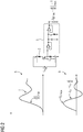
- FIG. 1 schematically shows a power semiconductor module 1, which has a plurality of power semiconductor devices 2 here.
- the power semiconductor module 1 here has a heat sink 3, on which the power semiconductor components 2 are arranged and which serves for cooling the power semiconductor components 2 during operation of the power semiconductor module 1.
- the geometric dimensions of the heat sink 3 are greater than those of the interconnected power semiconductor devices 2.
- the power semiconductor module 1 can be configured, for example, as a converter or as an inverter.
- the power semiconductor components 2 may be, for example, IGBTs.
- the power semiconductor module 1 During operation of the power semiconductor module 1, for example, it is exposed to thermal loads, through which the power semiconductor module 1 ages. This aging can lead to a shortening of a service life or a functionality of the power semiconductor module 1 and to a premature failure of the power semiconductor module 1.
- the aim of the method described below is to determine the aging of the power semiconductor module 1 during operation of the power semiconductor module 1 and thus to predict a remaining service life or availability of the power semiconductor module 1.
- a thermal model 4 of the power semiconductor module 1 is determined.
- the thermal model 4 here comprises matrices G S and G Z , which contain transfer functions. These transfer functions describe a thermal path of the power semiconductor module 1 and can be calculated from the measured thermal impedances of the power semiconductor devices 2.
- the thermal model 4 here comprises heat sources or heat sinks within the power semiconductor module 1, which are specified or characterized here via a power loss P or heat output and via a heat sink temperature T C of the heat sink 3.
- the thermal path may include a housing temperature and a thermal grease.
- the power loss P can be calculated at the operating point of the power semiconductor module 1 from an output voltage measured at the reference time and from an output current measured at the reference time.
- the heat sink temperature T C is measured during operation of the power semiconductor module 1.
- a reference temperature T j, zth is determined.
- a temperature-sensitive electrical parameter TSEP may include, for example, a threshold voltage (gate-emitter voltage), a miller plateau, a turn-on delay time, a turn-off delay time, a current slew rate, a flyback charge, a tail current, a voltage peak between emitter and auxiliary emitter during a turn-on operation, and an input and a Off duration of the power semiconductor module 1 be.
- a current temperature T j, tsep of the power semiconductor module 1 is determined.
- the determination of the current temperature T j, tsep can be done for example by means of a predetermined characteristic curve 6.
- Characteristic 6 plots values for a temperature-sensitive electrical parameter over the temperature.
- the characteristic curve 6 may, for example, have been determined at a calibration time, in particular before the power semiconductor module 1 is put into operation.
- the power semiconductor module 1 was set to predetermined temperature values, for example heated, measured at the predetermined, set temperature value of the corresponding temperature-sensitive electrical parameters and the respective value pairs shown in the characteristic curve 6.
- the at least one temperature-sensitive electrical parameter TSEP for example by means of the measuring circuit 5, is detected, the current temperature T j, tsep of the power semiconductor module 1 can be determined in a particularly simple and fast manner by means of the predetermined characteristic curve 6.
- the detection of the at least one temperature-sensitive electrical parameter TSEP can be carried out, for example, continuously or at predetermined measuring times during operation of the power semiconductor module 1.
- the temperature difference .DELTA.T can for example be provided to a control device 7, which is designed to regulate a power of the power semiconductor module 1 as a function of the temperature difference .DELTA.T.
- a control device 7 which is designed to regulate a power of the power semiconductor module 1 as a function of the temperature difference .DELTA.T.
- FIG. 2 shows an example of a measuring circuit 5 for measuring temperature-sensitive electrical parameters TSEP of a power semiconductor component 2 and two characteristic curves 8 and 9.
- a current waveform I is shown at a switch-on of the power semiconductor device 2.
- a voltage drop U EE ' at a leakage inductance L st between an emitter terminal E of the power semiconductor component 2 and a so-called auxiliary emitter E' of the semiconductor power component 2 is shown.
- max and from this a voltage peak U EE'max determined during a switch-on of the power semiconductor device 2.
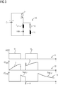
- FIG. 3 shows a double pulse measuring circuit 10 for performing a double pulse test with an input characteristic 11 and two output characteristics 12 and 13.
- These measuring circuit 10 and the characteristic curves 11, 12 and 13 are made of " Semiconductor Power Devices "(Josef Lutz, Springer-Verlag Berlin Heidelberg 2006, p 126/127 ) known.
- the double-pulse experiment can be used, for example, to measure temperature-sensitive electrical parameters TSEP, for example a reverse current peak 14 predetermined temperature can be used to create the characteristic curve 6.
- the double-pulse measuring circuit 10 comprises the IGBT designed semiconductor power device 2, a capacitor C, a resistor R and a coil L, which form an ohmschinduktive load, a freewheeling diode FWD, and a parasitic inductance L par , which due to the lines between the capacitor C , the semiconductor power device 2 and the diode FWD is formed.
- a first voltage pulse U 1 is generated at the input of the semiconductor power component 2, which is plotted in characteristic curve 11 over the time t.
- the current profile I 1 of the semiconductor power component 2 during the first voltage pulse U 1 is plotted in characteristic curve 12 over the time t.
- the current I FWD, 1 is taken over by the freewheeling diode FWD whose current characteristic is plotted in characteristic curve 13 over the time t.
- the diode FWD is commutated and the semiconductor power device 2 takes over the additional reverse current 14 of the diode FWD when switching on, which is the temperature-sensitive electrical parameter TSEP at the predetermined temperature is detected.
Description
Die Erfindung betrifft ein Verfahren zum Charakterisieren eines Leistungshalbleitermoduls aufweisend zumindest ein Leistungshalbleiterbauelement. Die Erfindung betrifft außerdem eine Vorrichtung sowie eine Schaltungsanordnung.The invention relates to a method for characterizing a power semiconductor module having at least one power semiconductor component. The invention also relates to a device and a circuit arrangement.
Leistungshalbleitermodule sind bereits aus dem Stand der Technik bekannt und können beispielsweise einen Wechselrichter oder einen Umrichter umfassen. Leistungshalbleitermodule umfassen in der Regel zumindest einen Leistungshalbleiterchip beziehungsweise ein Leistungshalbleiterbauelement, welches insbesondere für das Steuern und Schalten hoher elektrischer Ströme und Spannungen ausgelegt ist. Ein solches Leistungshalbleiterbauelement kann beispielsweise ein Leistungs-Metall-Oxid-Feldeffekttransitor (Leistungs-MOSFET), eine Leistungsdiode oder ein Bipolartransistor mit isolierter Gate-Elektrode (insulated-gate bipolar transistor, kurz IGBT) sein. Die Leistungshalbleiterbauelemente werden zum Ausbilden des Leistungshalbleitermoduls üblicherweise auf ein Substrat gelötet und durch Bondverbindungen elektrisch miteinander verbunden.Power semiconductor modules are already known from the prior art and may include, for example, an inverter or a converter. Power semiconductor modules generally comprise at least one power semiconductor chip or a power semiconductor component, which is designed in particular for controlling and switching high electrical currents and voltages. Such a power semiconductor device may be, for example, a power metal oxide field effect transistor (power MOSFET), a power diode or an insulated gate bipolar transistor (IGBT). The power semiconductor components are usually soldered onto a substrate to form the power semiconductor module and electrically connected to one another by bond connections.
Leistungshalbleitermodule können über ihre Lebensdauer charakterisiert werden. Die Lebensdauer des Leistungshalbleitermoduls ist eine Zeit bis zu einem Ausfall beziehungsweise einer Funktionsuntüchtigkeit des Leistungshalbleitermoduls. Während eines Betriebs des Leistungshalbleitermoduls kann sich eine verbleibende Lebensdauer des Leistungshalbleitermoduls, eine sogenannte Restlebensdauer des Leistungshalbleitermoduls, beispielsweise durch eine Alterung des Leistungshalbleitermoduls verändern. Dabei gilt insbesondere, dass sich die Restlebensdauer des Leistungshalbleitermoduls verkürzt, je schneller das Leistungsmodul altert.Power semiconductor modules can be characterized over their lifetime. The life of the power semiconductor module is a time to failure or a malfunction of the power semiconductor module. During operation of the power semiconductor module, a remaining service life of the power semiconductor module, a so-called remaining service life of the power semiconductor module, may change, for example as a result of aging of the power semiconductor module. It is especially true that the remaining life of the power semiconductor module shortens the faster the power module ages.
Die Alterung des Leistungshalbleitermoduls wird in der Regel während des Betriebs, in welchem die Leistungshalbleitermodule thermischen und mechanischen Belastungen ausgesetzt sein können, beschleunigt. Diese thermischen und mechanischen Belastungen der Leistungshalbleitermodule können zu einer sogenannten thermomechanischen Ermüdung des Leistungshalbleitermoduls führen, welche den Ausfall beziehungsweise eine Funktionsuntüchtigkeit des Leistungshalbleitermoduls und damit ein Ende der Lebensdauer zur Folge haben kann. Thermische Belastungen können beispielsweise Temperaturwechselbelastungen durch den elektrischen Betrieb des Leistungshalbleitermoduls sein, welche insbesondere aufgrund unterschiedlicher thermischer Ausdehnungskoeffizienten der Materialien im Leistungshalbleitermodul zu einer Ermüdung der elektrischen Verbindungsstellen, beispielsweise von Bondverbindungen und Lötverbindungen des Chiplotes und des Systemlotes, führen können. Durch die Ermüdung der Verbindungsstellen können sich beispielsweise die Bondverbindungen oder die Lötverbindungen lösen, was zu einer erhöhten Temperatur des Halbleiterchips führt. Insgesamt wird also durch die thermomechanische Ermüdung des Leistungshalbleitermoduls die Alterung des Leistungshalbleitermoduls beschleunigt, was zu einer reduzierten Restlebensdauer und zu einem verfrühten Ausfall des Leistungshalbleitermoduls führen kann.The aging of the power semiconductor module is usually accelerated during operation, in which the power semiconductor modules can be exposed to thermal and mechanical stresses. These thermal and mechanical loads of the power semiconductor modules can lead to a so-called thermo-mechanical fatigue of the power semiconductor module, which can result in the failure or inoperability of the power semiconductor module and thus an end to the life. Thermal loads can be, for example, thermal cycling due to the electrical operation of the power semiconductor module, which, in particular due to different thermal expansion coefficients of the materials in the power semiconductor module to fatigue of the electrical connection points, such as bonds and solder joints of the chip solder and the system solder lead. Due to the fatigue of the connection points, for example, the bond connections or the solder joints may become loose, which leads to an increased temperature of the semiconductor chip. Overall, therefore, the aging of the power semiconductor module is accelerated by the thermo-mechanical fatigue of the power semiconductor module, which can lead to a reduced residual life and to a premature failure of the power semiconductor module.
Um einen sicheren Betrieb des Leistungshalbleitermoduls innerhalb seines Anwendungsgebietes zu gewährleisten, ist eine Vorhersage der Lebensdauer des Leistungshalbleitermoduls wünschenswert. Gemäß dem Stand der Technik werden zum Vorhersagen der Lebensdauer der Leistungshalbleitermodule Lebensdauerberechnungen anhand von Lebensdauerkurven und vorgegebenen Lastprofilen rechnergestützt durchgeführt. Dazu wird beispielsweise eine Temperatur der Leistungshalbleitermodule überwacht, indem beispielsweise Thermistoren zusammen mit den Leistungshalbleiterbauelementen auf das Substrat gelötet werden. Jedoch lassen sich durch die räumliche Entfernung der Thermistoren zu den Leistungshalbleiterbauelementen die exakten transienten Temperaturen der Chips nicht genau erfassen, wodurch keine genauen Lebensdauerberechnungen durchgeführt werden können.In order to ensure safe operation of the power semiconductor module within its field of application, a prediction of the lifetime of the power semiconductor module is desirable. According to the state of the art, lifetime calculations of lifetime curves of the power semiconductor modules are performed on the basis of lifetime curves and predetermined load profiles in a computer-aided manner. For this purpose, for example, a temperature of the power semiconductor modules is monitored by, for example, thermistors being soldered together with the power semiconductor components to the substrate. However, due to the spatial distance of the thermistors to the power semiconductor devices, the exact transient temperatures of the chips can not be accurately detected, whereby no accurate lifetime calculations can be performed.
Auch ist aus dem Stand der Technik bekannt, thermische Ersatzschaltbilder für die Leistungshalbleitermodule zu erstellen, anhand welcher indirekt auf die Temperatur der Leistungshalbleiterbauelemente geschlossen werden kann. Über Strom- und Spannungsmessungen beziehungsweise über die Kenntnis des Arbeitspunktes des Leistungshalbleitermoduls lassen sich die elektrischen Verluste der IGBTs und der Dioden berechnen. Somit können zwar die Temperaturen der Leistungshalbleiterbauelemente im Betrieb berechnet werden, jedoch wird in den thermischen Ersatzschaltbildern in der Regel keine Alterung der Leistungshalbleiterbauelemente berücksichtigt.It is also known from the prior art to create thermal equivalent circuit diagrams for the power semiconductor modules, on the basis of which the temperature of the power semiconductor components can be indirectly deduced. Current and voltage measurements or the knowledge of the operating point of the power semiconductor module, the electrical losses of the IGBTs and the diodes can be calculated. Thus, while the temperatures of the power semiconductor devices can be calculated during operation, but in the thermal equivalent circuit diagrams usually no aging of the power semiconductor devices is taken into account.
Hierzu beschreibt die
Zudem offenbart die
Schließlich beschreibt die
Es ist Aufgabe der vorliegenden Erfindung, eine Lösung bereitzustellen, durch welche eine Alterung von Leistungshalbleitermodulen zuverlässiger bestimmt und dadurch eine Restlebensdauer der Leistungshalbleitermodule genauer vorhergesagt werden kann.It is an object of the present invention to provide a solution by means of which an aging of power semiconductor modules can be determined more reliably and thus a residual service life of the power semiconductor modules can be predicted more accurately.
Diese Aufgabe wird erfindungsgemäß durch ein Verfahren, eine Vorrichtung sowie eine Schaltungsanordnung mit den Merkmalen gemäß den jeweiligen unabhängigen Patentansprüchen gelöst. Vorteilhafte Ausführungen der Erfindung sind Gegenstand der abhängigen Patentansprüche, der Beschreibung und der Figuren.This object is achieved by a method, an apparatus and a circuit arrangement with the features according to the respective independent claims. Advantageous embodiments of the invention are the subject of the dependent claims, the description and the figures.
Ein erfindungsgemäßes Verfahren dient zum Charakterisieren eines Leistungshalbleitermoduls mit zumindest einem Leistungshalbleiterbauelement. Bei dem Verfahren wird ein thermisches Modell des Leistungshalbleitermoduls zu einem Referenzzeitpunkt bestimmt, welcher vor einer Inbetriebnahme des Leistungshalbleitermoduls liegt, wobei zum Erstellen des thermischen Modells eine einen thermischen Pfad des Leistungshalbleitermoduls beschreibende thermische Impedanz des Leistungshalbleitermoduls bestimmt wird. Zudem wird eine Referenztemperatur anhand des thermischen Modells des Leistungshalbleitermoduls ermittelt, zumindest ein temperatursensitiver elektrischer Parameter (TSEP) des Leistungshalbleitermoduls zu zumindest einem gegenüber dem Referenzzeitpunkt späteren Zeitpunkt im Betrieb des Leistungshalbleitermoduls gemessen, eine aktuelle Temperatur des Leistungshalbleitermoduls aus dem zumindest einen gemessenen temperatursensitiven elektrischen Parameter des Leistungshalbleitermoduls ermittelt, eine Temperaturdifferenz zwischen der aktuellen Temperatur und der Referenztemperatur ermittelt und eine Alterung des Leistungshalbleitermoduls anhand der ermittelten Temperaturdifferenz bestimmt.A method according to the invention serves to characterize a power semiconductor module having at least one power semiconductor component. In the method, a thermal model of the power semiconductor module is determined at a reference time, which is before startup of the power semiconductor module, wherein a thermal impedance of the power semiconductor module describing a thermal path of the power semiconductor module is determined to create the thermal model. In addition, a reference temperature based on the thermal model of the power semiconductor module determined, at least one temperature-sensitive electrical parameter (TSEP) of the power semiconductor module to at least one compared to the reference time later time measured during operation of the power semiconductor module, a current temperature of the power semiconductor module from the at least one measured temperature-sensitive electrical parameter of the power semiconductor module determines a temperature difference between the current temperature and the reference temperature is determined and determines an aging of the power semiconductor module based on the determined temperature difference.
Das Leistungshalbleitermodul kann beispielsweise einen Wechselrichter oder einen Umrichter umfassen und weist bevorzugt einen IGBT als das zumindest eine Leistungshalbleiterbauelement auf. Um nun eine Lebensdauer des Leistungshalbleitermoduls vorherzusagen, wird die Alterung beziehungsweise ein Alterungsfortschritt des Leistungshalbleitermoduls bestimmt. Dazu wird für das Leistungshalbleitermodul das das Leistungshalbleitermodul charakterisierende thermische Modell zu dem Referenzzeitpunkt bestimmt. Das thermische Modell dient zur Beschreibung des thermischen Verhaltens des Leistungshalbleitermoduls. In dem thermischen Modell werden insbesondere Wärmequellen oder Wärmesenken innerhalb des Leistungshalbleitermoduls berücksichtigt. Solche Wärmequellen werden vorzugsweise über eine Verlustleistung des Leistungshalbleitermoduls, welche anhand von Strom- und Spannungsmessungen bestimmt werden kann, berechnet.The power semiconductor module may comprise, for example, an inverter or a converter and preferably has an IGBT as the at least one power semiconductor component. In order to predict a lifetime of the power semiconductor module, the aging or an aging progress of the power semiconductor module is determined. For this purpose, the thermal semiconductor module characterizing the power semiconductor module at the reference time is determined for the power semiconductor module. The thermal model is used to describe the thermal behavior of the power semiconductor module. In particular, heat sources or heat sinks within the power semiconductor module are taken into account in the thermal model. Such heat sources are preferably calculated via a power loss of the power semiconductor module, which can be determined by means of current and voltage measurements.
Zu dem Referenzzeitpunkt, zu welchem das thermische Modell bestimmt wird, weist das Leistungshalbleitermodul einen nicht gealterten Zustand, welcher auch als ein gesunder Zustand des Leistungshalbleitermoduls bezeichnet wird, auf, in welchem das Leistungshalbleitermodul insbesondere keine Ermüdungserscheinungen beziehungsweise Verschleißerscheinungen zeigt. Dieser Referenzzeitpunkt liegt vor einer Inbetriebnahme des Leistungshalbleitermoduls. Dies bedeutet, dass das Leistungshalbleitermodul noch keinen thermomechanischen Belastungen, welche üblicherweise zu der Ermüdung beziehungsweise beschleunigten Alterung des Leistungshalbleitermoduls führen, ausgesetzt war. Dieses zu dem Referenzzeitpunkt erstellte thermische Modell stellt also einen Anfangszustand des Leistungshalbleitermoduls dar.At the reference time at which the thermal model is determined, the power semiconductor module has a non-aged state, which is also referred to as a healthy state of the power semiconductor module, in which the power semiconductor module in particular shows no signs of wear or wear. This reference time is before commissioning of the power semiconductor module. This means that the power semiconductor module does not yet have thermomechanical loads, which was usually the fatigue or accelerated aging of the power semiconductor module, was exposed. This thermal model created at the reference time thus represents an initial state of the power semiconductor module.
Anhand dieses thermischen Modells wird die Referenztemperatur des Leistungshalbleitermoduls, welche einer sogenannten Sperrschichttemperatur entspricht, ermittelt. Durch diese Referenztemperatur wird der ungealterte Zustand beziehungsweise der gesunde Zustand des Leistungshalbleitermoduls charakterisiert. Beispielsweise kann bei einem thermischen Modell, welches das Leistungshalbleitermodul über die Verlustleistung charakterisiert, aus den bekannten Zusammenhängen zwischen Verlustleistung und Temperatur direkt die Referenztemperatur berechnet werden.On the basis of this thermal model, the reference temperature of the power semiconductor module, which corresponds to a so-called junction temperature, is determined. This reference temperature characterizes the unaged state or the healthy state of the power semiconductor module. For example, in a thermal model, which characterizes the power semiconductor module via the power loss, the reference temperature can be calculated directly from the known relationships between power loss and temperature.
Nach Bestimmen der Referenztemperatur wird zu dem späteren Zeitpunkt, welcher zeitlich nach dem Referenzzeitpunkt liegt, zumindest ein temperatursensitiver elektrischer Parameter des Leistungshalbleitermoduls im Betrieb des Leistungshalbleitermoduls, beispielsweise in einem Wechselrichterbetrieb des den Wechselrichter aufweisenden Leistungshalbleitermoduls, gemessen. Während des Betriebs, also während einer bestimmungsgemäßen Verwendung des Leistungshalbleitermoduls, ist das Leistungshalbleitermodul thermomechanischen Belastungen ausgesetzt, durch welche das Leistungshalbleitermodul altern kann. Die Messung kann kontinuierlich oder zu vorbestimmten Messzeitpunkten während des Betriebs des Leistungshalbleitermoduls erfolgen.After determining the reference temperature, at least one temperature-sensitive electrical parameter of the power semiconductor module during operation of the power semiconductor module, for example in an inverter operation of the power semiconductor module having the inverter, is measured at the later time, which is later than the reference time. During operation, that is, during intended use of the power semiconductor module, the power semiconductor module is exposed to thermo-mechanical loads, which may cause the power semiconductor module to age. The measurement can be carried out continuously or at predetermined measuring times during operation of the power semiconductor module.
Zur Messung des zumindest einen temperatursensitiven elektrischen Parameters des Leistungshalbleitermoduls kann beispielsweise eine entsprechende Messschaltung bereitgestellt werden. Auch kann vorgesehen sein, dass das Leistungshalbleitermodul oder das zumindest eine Leistungshalbleiterelement eine integrierte Messeinrichtung, beispielsweise eine Diode, aufweist, anhand welcher eine Temperaturüberwachung der Leistungshalbleitermodule durchgeführt werden kann.For example, a corresponding measuring circuit can be provided for measuring the at least one temperature-sensitive electrical parameter of the power semiconductor module. It can also be provided that the power semiconductor module or the at least one power semiconductor element has an integrated measuring device, for example a diode, has, by means of which a temperature monitoring of the power semiconductor modules can be performed.
Aus dem zumindest einen temperatursensitiven elektrischen Parameter wird eine aktuelle Temperatur, also eine Temperatur, welche das Leistungshalbleitermodul zu dem jeweiligen Messzeitpunkt aufweist, ermittelt beziehungsweise berechnet. Diese aktuelle Temperatur wird mit der Referenztemperatur verglichen und die Temperaturdifferenz zwischen der Referenztemperatur und der aktuellen Temperatur bestimmt.From the at least one temperature-sensitive electrical parameter is a current temperature, ie a temperature which has the power semiconductor module at the respective measurement time, determined or calculated. This current temperature is compared with the reference temperature and the temperature difference between the reference temperature and the current temperature is determined.
Der Erfindung liegt die Erkenntnis zugrunde, dass sich während der Alterung des Leistungshalbleitermoduls beispielsweise durch Verschleißerscheinungen, insbesondere durch das bereits beschriebene Lösen von Bond- oder Lötverbindungen, eine Temperatur des Leistungshalbleitermoduls im Vergleich zu der Referenztemperatur des Leistungshalbleitermoduls im gesunden Zustand verändert. Durch das Lösen der Lötverbindung kann beispielsweise eine durch das Leistungshalbleiterbauelement im Betrieb produzierte Wärme nicht mehr oder nur schlecht über die Lötverbindung abgeführt werden. Dadurch kann sich die aktuelle Temperatur der Leistungshalbleitermoduls im Betrieb erhöhen.The invention is based on the finding that during the aging of the power semiconductor module, for example due to wear, in particular by the already described release of bonding or solder joints, a temperature of the power semiconductor module changes in the healthy state compared to the reference temperature of the power semiconductor module. By dissolving the solder connection, for example, a heat produced by the power semiconductor component during operation can no longer be dissipated or only poorly dissipated via the solder connection. As a result, the current temperature of the power semiconductor module can increase during operation.
Anhand der Temperaturdifferenz kann eine Alterung des Leistungshalbleitermoduls abgeschätzt beziehungsweise bestimmt werden. In einem ungealterten Zustand ist diese Temperaturdifferenz etwa Null. Mit fortschreitender Alterung und zunehmenden Verschleißerscheinungen erhöht sich die Temperaturdifferenz zunehmend, wobei die relative Änderung der Temperaturdifferenz einen Hinweis auf ein alterndes Leistungshalbleitermodul liefert.Based on the temperature difference, aging of the power semiconductor module can be estimated or determined. In an unaged condition, this temperature difference is about zero. As the aging progresses and the signs of wear increase, the temperature difference increases, with the relative change in the temperature difference providing an indication of an aging power semiconductor module.
Mittels des erfindungsgemäßen Verfahrens kann also auf besonders einfache Weise durch Ermitteln der Temperaturdifferenz eine Alterung des Leistungshalbleitermoduls bestimmt werden und damit eine Restlebensdauer beziehungsweise eine Verfügbarkeit des Halbleitermoduls vorhergesagt werden. Dadurch kann ein zuverlässiger Betrieb des Leistungshalbleitermoduls in seinem jeweiligen Anwendungsgebiet gewährleistet werden. Dadurch, dass die Alterung während des Betriebs beziehungsweise während der Betriebsphasen des Leistungshalbleitermoduls bestimmt wird, kann in vorteilhafter Weise eine Unterbrechung des Betriebs des Leistungshalbleitermoduls vermieden werden. Das Verfahren ist daher besonders anwenderfreundlich gestaltet.Thus, by means of the method according to the invention, an aging of the power semiconductor module can be determined in a particularly simple manner by determining the temperature difference, and thus a remaining service life or availability of the semiconductor module can be predicted. Thereby a reliable operation of the power semiconductor module can be ensured in its respective field of application. Because the aging is determined during operation or during the operating phases of the power semiconductor module, an interruption of the operation of the power semiconductor module can be avoided in an advantageous manner. The method is therefore designed to be particularly user-friendly.
Zusätzlich kann durch das Ermitteln der Alterung eine temperaturdifferenzabhängige Leistungsregelung des Leistungshalbleitermoduls zum Vermeiden von erhöhten Betriebstemperaturen und Temperaturwechselbelastungen bereitgestellt werden. Beispielsweise kann eine Steuereinrichtung bereitgestellt werden, welche anhand der ermittelten Temperaturdifferenz eine entsprechende Leistungsregelung für einen effizienten Betrieb des Leistungshalbleitermoduls durchführt. Somit kann durch den effizienten Betrieb des Leistungshalbleitermoduls einer fortschreitenden Alterung und damit einem verfrühten Ausfall des Leistungshalbleitermoduls entgegengewirkt werden.In addition, by determining the aging, a temperature-difference-dependent power control of the power semiconductor module can be provided to avoid increased operating temperatures and thermal cycling. For example, a control device can be provided which, on the basis of the determined temperature difference, performs a corresponding power control for efficient operation of the power semiconductor module. Thus, by the efficient operation of the power semiconductor module, a progressive aging and thus a premature failure of the power semiconductor module can be counteracted.
Zum Erstellen des thermischen Modells wird eine einen thermischen Pfad des Leistungshalbleitermoduls beschreibende thermische Impedanz des Leistungshalbleitermoduls bestimmt. Die thermische Impedanz des Leistungshalbleitermoduls wird zu dem Referenzzeitpunkt, zu welchem das Leistungshalbleitermodul den Anfangszustand beziehungsweise den ungealterten Zustand aufweist, ermittelt beziehungsweise gemessen. Mittels der thermischen Impedanz kann der thermische Pfad des Leistungshalbleitermoduls beschrieben beziehungsweise parametrisiert werden. Die thermische Impedanz ist ein Wärmekennwert und ein Maß für einen Temperaturunterschied, welcher in dem Leistungshalbleitermodul, beim Hindurchtreten eines Wärmestromes entsteht. Bei Leistungshalbleitermodulen, welche eine Zusammenschaltung mehrere Leistungshalbleiterbauelemente aufweisen, setzt sich die thermische Impedanz des Leistungshalbleitermoduls aus den einzelnen thermischen Impedanzen der Leistungshalbleiterbauelemente zusammen. Die thermische Impedanz kann beispielsweise aus einem thermischen Ersatzschaltbild berechnet werden. Dazu können die das thermische Verhalten beschreibenden Kenngrößen in elektrische Größen übertragen werden. Mit diesen elektrischen Größen kann ein elektrisches Netzwerk erstellt werden, welches analytisch oder mittels eines Schaltungssimulators berechnet werden kann. Durch das Ermitteln der thermischen Impedanz kann ein besonders genaues und verlässliches Modell des Leistungshalbleitermoduls bestimmt werden.To create the thermal model, a thermal impedance of the power semiconductor module describing a thermal path of the power semiconductor module is determined. The thermal impedance of the power semiconductor module is determined or measured at the reference time at which the power semiconductor module has the initial state or the unaged state. By means of the thermal impedance, the thermal path of the power semiconductor module can be described or parameterized. The thermal impedance is a thermal characteristic and a measure of a temperature differential that arises in the power semiconductor module as a heat flow passes therethrough. In the case of power semiconductor modules which have an interconnection of a plurality of power semiconductor components, the thermal impedance of the power semiconductor module is composed of the individual thermal impedances of the power semiconductor components. The thermal impedance can for example be calculated from a thermal equivalent circuit diagram. For this purpose, the characteristics describing the thermal behavior can be transferred into electrical quantities. With these electrical quantities, an electrical network can be created, which can be calculated analytically or by means of a circuit simulator. By determining the thermal impedance, a particularly accurate and reliable model of the power semiconductor module can be determined.
Bevorzugt wird zum Erstellen des thermischen Modells eine Verlustleistung beziehungsweise eine Wärmeleistung des Leistungshalbleitermoduls bestimmt. Die Wärmeleistung beziehungsweise die Verlustleistung wird insbesondere in dem Arbeitspunkt des Leistungshalbleitermoduls durch Messen der Ausgangsspannung und des Ausgangsstroms des Leistungshalbleitermoduls und durch Bilden des Produktes von Ausgangsspannung und Ausgangsstrom berechnet. Anhand der Bestimmung der Wärmeleistung des Leistungshalbleitermoduls kann auf besonders einfache Weise das thermische Modell erstellt werden.Preferably, a power loss or a heat output of the power semiconductor module is determined to create the thermal model. The heat output or the power loss is calculated in particular in the operating point of the power semiconductor module by measuring the output voltage and the output current of the power semiconductor module and by forming the product of output voltage and output current. Based on the determination of the heat output of the power semiconductor module, the thermal model can be created in a particularly simple manner.
Vorzugsweise wird zum Erstellen des thermischen Modells eine Temperatur eines Kühlkörpers des Leistungshalbleitermoduls im Betrieb des Leistungshalbleitermoduls erfasst. Ein solcher Kühlkörper kann beispielsweise eine Kühlplatte sein, deren Temperatur im Betrieb des Leistungshalbleitermoduls gemessen wird. Der Kühlkörper als eine Wärmequelle beziehungsweise eine Wärmesenke kann also ebenfalls in dem thermischen Modell berücksichtigt werden, wodurch das thermische Modell besonders genau und zuverlässig gestaltet ist.Preferably, to create the thermal model, a temperature of a heat sink of the power semiconductor module is detected during operation of the power semiconductor module. Such a heat sink may for example be a cooling plate whose temperature is measured during operation of the power semiconductor module. The heat sink as a heat source or a heat sink can thus also be taken into account in the thermal model, whereby the thermal model is designed particularly accurate and reliable.
Vorzugsweise wird als der zumindest eine temperatursensitive elektrische Parameter des Leistungshalbleitermoduls, welches als das zumindest eine Leistungshalbleiterbauelement bevorzugt einen IGBT aufweist, zumindest eine der folgenden Größen gemessen: eine elektrische Schwellenspannung, also eine Gate-Emitter-Spannung, ein Millerplateau, eine Einschaltverzögerungszeit des Leistungshalbleitermoduls, eine Ausschaltverzögerungszeit des Leistungshalbleitermoduls, eine Stromanstiegsgeschwindigkeit, eine Sperrverzugsladung beziehungsweise eine Sperrverzögerungsladung, ein Tailstrom, welcher die Ausschaltverluste des Leistungshalbleitermoduls charakterisiert, eine Spannungsspitze des Leistungshalbleitermoduls während eines Einschaltvorgangs, eine Einschaltdauer des Leistungshalbleitermoduls oder eine Ausschaltdauer des Leistungshalbleitermoduls. Da jede dieser Größen temperaturabhängig ist, kann aus den gemessenen Werten dieser Größen auf besonders einfache Weise eine aktuelle Temperatur des Leistungshalbleitermoduls bestimmt werden.Preferably, at least one of the following variables is measured as the at least one temperature-sensitive electrical parameter of the power semiconductor module which preferably has an IGBT as the at least one power semiconductor component: an electrical threshold voltage, ie a gate-emitter voltage, a miller plateau, a switch-on delay time of the power semiconductor module, a switch-off delay time the power semiconductor module, a current rise speed, a reverse charge delay or a reverse recovery charge, a tail current, which characterizes the turn-off of the power semiconductor module, a voltage peak of the power semiconductor module during a power-on, a turn-on of the power semiconductor module or a turn-off of the power semiconductor module. Since each of these variables is temperature-dependent, a current temperature of the power semiconductor module can be determined in a particularly simple manner from the measured values of these variables.
In einer Ausführungsform der Erfindung wird eine Kennlinie für das Leistungshalbleitermodul bestimmt, anhand welcher jedem Wert des zumindest einen temperatursensitiven elektrischen Parameters jeweils ein Temperaturwert zugeordnet wird, wobei einer der Temperaturwerte in Abhängigkeit des gemessenen temperatursensitiven elektrischen Parameters als die aktuelle Temperatur bestimmt wird. Diese Kennlinie wird insbesondere einmalig zu einem Kalibrierzeitpunkt, beispielsweise in dem gesunden Zustand des Leistungshalbleitermoduls, bestimmt. In dieser Kennlinie sind Werte des zumindest einen temperatursensitiven elektrischen Parameters über die Temperatur aufgetragen. Zu dem späteren Zeitpunkt kann anhand dieser vorgegebenen Kennlinie besonders schnell und ohne großen Rechenaufwand die zu dem Wert des im Betrieb gemessenen temperatursensitiven elektrischen Parameters korrespondierende Temperatur als die aktuelle Temperatur bestimmt werden. Bei einer kontinuierlichen Messung der temperatursensitiven elektrischen Parameter im Betrieb des Leistungshalbleitermoduls können somit insbesondere eine Echtzeitmessung der Temperaturdifferenz und damit eine Online-Lebensdauerüberwachung erfolgen. Damit kann eine fortschreitende Alterung des Leistungshalbleitermoduls frühzeitig erkannt werden.In one embodiment of the invention, a characteristic curve for the power semiconductor module is determined on the basis of which each value of the at least one temperature-sensitive electrical parameter is assigned a temperature value, one of the temperature values being determined as the current temperature as a function of the measured temperature-sensitive electrical parameter. This characteristic is in particular determined once at a calibration time, for example in the healthy state of the power semiconductor module. In this characteristic, values of the at least one temperature-sensitive electrical parameter are plotted against the temperature. At the later time, the temperature corresponding to the value of the temperature-sensitive electrical parameter measured during operation can be determined as the current temperature particularly quickly and without great computational effort on the basis of this predetermined characteristic curve. In the case of a continuous measurement of the temperature-sensitive electrical parameters during operation of the power semiconductor module, a real-time measurement of the temperature difference and thus an online life-time monitoring can therefore take place in particular. Thus, a progressive aging of the power semiconductor module can be detected early.
Vorzugsweise wird die Kennlinie bestimmt, indem die Temperaturwerte für das Leistungshalbleitermodul vorgegeben werden, das Leistungshalbleitermodul auf den jeweiligen Temperaturwert temperiert beziehungsweise eingestellt wird und der jeweilige Wert des zumindest einen temperatursensitiven elektrischen Parameters bei dem vorgegebenen Temperaturwert gemessen wird. Mit anderen Worten bedeutet dies, dass die Temperatur des Leistungshalbleitermoduls aktiv auf die vorgegebenen Temperaturwerte eingestellt wird. Zum Einstellen der Temperatur wird in einer Ausführungsform der Erfindung eine Heizeinrichtung bereitgestellt, mittels welcher das Leistungshalbleitermodul auf die jeweiligen vorgegebenen Temperaturwerte aufgeheizt werden kann.The characteristic curve is preferably determined by specifying the temperature values for the power semiconductor module, the power semiconductor module to the respective temperature value is tempered or adjusted and the respective value of the at least one temperature-sensitive electrical parameter at the predetermined temperature value is measured. In other words, this means that the temperature of the power semiconductor module is actively set to the predetermined temperature values. For adjusting the temperature, in one embodiment of the invention, a heating device is provided, by means of which the power semiconductor module can be heated to the respective predetermined temperature values.
Zum Bestimmen der Werte des zumindest einen temperatursensitiven elektrischen Parameter bei den verschiedenen vorgegebenen Temperaturwerten kann die Temperatur des Leistungshalbleitermoduls mittels der Heizeinrichtung stufenweise erhöht werden. Sobald sich das Leistungshalbleitermodul bei der durch die Heizeinrichtung bereitgestellten Temperatur mit dem vorgegebenen Temperaturwert in einem thermisch eingeschwungenen Zustand befindet, wird der jeweilige Wert des zumindest einen temperatursensitiven elektrischen Parameters gemessen. Somit kann jedem Temperaturwert eindeutig ein Wert des jeweiligen temperatursensitiven elektrischen Parameters zugeordnet werden. Durch diese Kalibrierung der temperatursensitiven elektrischen Parameter kann zu dem späteren Zeitpunkt die aktuelle Temperatur des Leistungshalbleitermoduls im Betrieb besonders schnell und einfach bestimmt beziehungsweise aus der Kennlinie ausgelesen werden.In order to determine the values of the at least one temperature-sensitive electrical parameter at the various predetermined temperature values, the temperature of the power semiconductor module can be increased stepwise by means of the heating device. As soon as the power semiconductor module is in a thermally steady state at the temperature provided by the heater with the predetermined temperature value, the respective value of the at least one temperature-sensitive electrical parameter is measured. Thus, each temperature value can be uniquely assigned a value of the respective temperature-sensitive electrical parameter. As a result of this calibration of the temperature-sensitive electrical parameters, the current temperature of the power semiconductor module can be determined particularly quickly and easily during operation or read from the characteristic curve at the later time.
Besonders bevorzugt erfolgt die Messung des zumindest einen temperatursensitiven elektrischen Parameters zum Bestimmen der Kennlinie in Abhängigkeit der vorgegebenen Temperatur mittels einer Doppelpuls-Messschaltung. Eine solche Doppelpuls-Messschaltung ist beispielsweise aus "Halbleiter-Leistungsbauelemente" (Josef Lutz, Springer-Verlag Berlin Heidelberg 2006, S. 126/127) bekannt. Dabei werden in dem thermisch eingeschwungenen Zustand des Leistungshalbleitermoduls zwei Spannungspulse am Gate-Emitter-Anschluss des oder der IGBTs erzeugt, die Einschalt- und Ausschaltvorgänge des oder der IGBTs erfasst und anschließend die temperatursensitiven elektrischen Parameter (TSEP) in Abhängigkeit der vorgegebenen Temperatur ausgewertet.Particularly preferably, the measurement of the at least one temperature-sensitive electrical parameter for determining the characteristic as a function of the predetermined temperature by means of a double-pulse measuring circuit. Such a double-pulse measuring circuit is known for example from "semiconductor power devices" (Josef Lutz, Springer-Verlag Berlin Heidelberg 2006, p 126/127). In this case, two voltage pulses are generated at the gate-emitter terminal of the IGBTs or in the thermally steady state of the power semiconductor module, the turn-on and turn-off of or of the IGBTs and then evaluated the temperature-sensitive electrical parameters (TSEP) as a function of the predetermined temperature.
Die Erfindung umfasst außerdem eine Vorrichtung zum Charakterisieren eines Leistungshalbleitermoduls in einem Betrieb des Leistungshalbleitermoduls mit einer Messeinrichtung zum Messen zumindest eines temperatursensitiven elektrischen Parameters des Leistungshalbleitermoduls und einer Recheneinrichtung zum Ermitteln einer aktuellen Temperatur aus dem zumindest einen temperatursensitiven elektrischen Parameter zu zumindest einem gegenüber einem Referenzzeitpunkt, welcher vor einer Inbetriebnahme des Leistungshalbleitermoduls liegt, späteren Zeitpunkt, zum Berechnen einer Temperaturdifferenz zwischen einer vorgegebenen Referenztemperatur und der aktuellen Temperatur und zum Bestimmen einer Alterung des Leistungshalbleitermoduls anhand der ermittelten Temperaturdifferenz, wobei die Referenztemperatur anhand eines zu dem Referenzzeitpunkt bestimmten thermischen Modells ermittelt ist und wobei das thermische Modell anhand einer einen thermischen Pfad des Leistungshalbleitermoduls beschreibende thermische Impedanz des Leistungshalbleitermoduls bestimmt ist. Die Vorrichtung dient zu einer Online-Überwachung der Temperaturdifferenz, also zu einer kontinuierlichen Überwachung der Temperaturdifferenz, und damit zu einer kontinuierlichen Überwachung der verbleibenden Lebensdauer in einem Betrieb des Leistungshalbleitermoduls.The invention also includes an apparatus for characterizing a power semiconductor module in an operation of the power semiconductor module with a measuring device for measuring at least one temperature-sensitive electrical parameter of the power semiconductor module and a computing device for determining a current temperature from the at least one temperature-sensitive electrical parameter to at least one compared to a reference time, which before commissioning of the power semiconductor module, later time, for calculating a temperature difference between a predetermined reference temperature and the current temperature and determining an aging of the power semiconductor module based on the determined temperature difference, wherein the reference temperature is determined based on a thermal model determined at the reference time and wherein the describe thermal model by means of a thermal path of the power semiconductor module ibende thermal impedance of the power semiconductor module is determined. The device is used for an online monitoring of the temperature difference, that is to a continuous monitoring of the temperature difference, and thus to a continuous monitoring of the remaining life in an operation of the power semiconductor module.
Zur Erfindung gehört außerdem eine Schaltungsanordnung aufweisend ein Leistungshalbleitermodul mit zumindest einem Leistungshalbleiterbauelement und eine erfindungsgemäße Vorrichtung zum Bestimmen der Alterung des Leistungshalbleitermoduls.The invention also includes a circuit arrangement comprising a power semiconductor module having at least one power semiconductor component and a device according to the invention for determining the aging of the power semiconductor module.
Bevorzugt umfasst das Leistungshalbleitermodul einen Wechselrichter und zumindest einen Kühlkörper, wobei der Wechselrichter als das zumindest eine Leistungshalbleiterbauelement zumindest einen IGBT aufweist.The power semiconductor module preferably comprises an inverter and at least one heat sink, wherein the inverter has at least one IGBT as the at least one power semiconductor component.
Gemäß einer Weiterbildung der Schaltungsanordnung umfasst die Schaltungsanordnung eine Steuereinrichtung, welche dazu ausgelegt ist, anhand der ermittelten Temperaturdifferenz eine Leistung des Leistungshalbleitermoduls zu regeln.According to one development of the circuit arrangement, the circuit arrangement comprises a control device which is designed to regulate a power of the power semiconductor module on the basis of the determined temperature difference.
Die mit Bezug auf das erfindungsgemäße Verfahren vorgestellten bevorzugten Ausführungsformen und deren Vorteile gelten entsprechend für die erfindungsgemäße Vorrichtung sowie für die erfindungsgemäße Schaltungsanordnung.The preferred embodiments presented with reference to the method according to the invention and their advantages apply correspondingly to the device according to the invention and to the circuit arrangement according to the invention.
Im Folgenden wird die Erfindung nun anhand eines bevorzugten Ausführungsbeispiels wie auch unter Bezugnahme auf die beigefügten Zeichnungen näher erläutert.In the following, the invention will now be explained in more detail with reference to a preferred embodiment as well as with reference to the accompanying drawings.
Es zeigen:
- FIG 1
- eine schematische Darstellung eines Leistungshalbleitermoduls, an welchem eine Ausführungsform des erfindungsgemäßen Verfahrens zur Bestimmung einer Alterung des Leistungshalbleitermoduls durchgeführt wird;
- FIG 2
- eine schematische Darstellung einer Messschaltung zur Messung von temperatursensitiven elektrischen Parametern eines Leistungshalbleiterbauelementes sowie dazugehörige Kennlinien des Leistungshalbleiterbauelementes; und
- FIG 3
- eine schematische Darstellung einer Doppelpuls-Messschaltung zum Durchführen eines Doppelpulsversuches mit zugehörigen Eingangs- und Ausgangskennlinien.
- FIG. 1
- a schematic representation of a power semiconductor module to which an embodiment of the method according to the invention for determining an aging of the power semiconductor module is performed;
- FIG. 2
- a schematic representation of a measuring circuit for measuring temperature-sensitive electrical parameters of a power semiconductor device and associated characteristics of the power semiconductor device; and
- FIG. 3
- a schematic representation of a double pulse measuring circuit for performing a double pulse test with associated input and output characteristics.
Bei dem im Folgenden erläuterten Ausführungsbeispiel handelt es sich um eine bevorzugte Ausführungsform der Erfindung. Bei dem Ausführungsbeispiel stellen aber die beschriebenen Komponenten der Ausführungsform jeweils einzelne, unabhängig voneinander zu betrachtende Merkmale der Erfindung dar, welche die Erfindung auch jeweils unabhängig voneinander weiterbilden und damit auch einzeln oder in einer anderen als der gezeigten Kombination als Bestandteil der Erfindung anzusehen sind. Des Weiteren ist die beschriebene Ausführungsform auch durch weitere der bereits beschriebenen Merkmale der Erfindung ergänzbar.The exemplary embodiment explained below is a preferred embodiment of the invention. In the embodiment, however, the described components of the embodiment each individually, independently to be considered features of the invention, which each further independently develop the invention and thus individually or in any other than the combination shown are to be regarded as part of the invention. Furthermore, the described embodiment can also be supplemented by further features of the invention already described.
Im Betrieb des Leistungshalbleitermoduls 1 ist dieses beispielsweise thermischen Belastungen ausgesetzt, durch welche das Leistungshalbleitermodul 1 altert. Diese Alterung kann zu einer Verkürzung einer Lebensdauer beziehungsweise einer Funktionstüchtigkeit des Leistungshalbleitermoduls 1 und zu einem verfrühten Ausfall des Leistungshalbleitermoduls 1 führen. Ziel des im Folgenden beschriebenen Verfahrens ist es, die Alterung des Leistungshalbleitermoduls 1 im Betrieb des Leistungshalbleitermoduls 1 zu bestimmen und damit eine verbleibende Lebensdauer beziehungsweise Verfügbarkeit des Leistungshalbleitermoduls 1 vorherzusagen.During operation of the
Zu einem Referenzzeitpunkt, zu welchem das Leistungshalbleitermodul 1 einen gesunden, ungealterten Zustand aufweist, wird ein thermisches Modell 4 des Leistungshalbleitermoduls 1 bestimmt. Das thermische Modell 4 umfasst hier Matrizen G S und G Z, welche Übertragungsfunktionen enthalten. Diese Übertragungsfunktionen beschreiben einen thermischen Pfad des Leistungshalbleitermoduls 1 und können aus den gemessenen thermischen Impedanzen der Leistungshalbleiterbauelemente 2 berechnet werden. Außerdem umfasst das thermische Modell 4 hier Wärmequellen beziehungsweise Wärmesenken innerhalb des Leistungshalbleitermoduls 1, welcher hier über eine Verlustleistung P beziehungsweise Wärmeleistung sowie über eine Kühlkörpertemperatur TC des Kühlkörpers 3 angegeben beziehungsweise charakterisiert werden. Auch kann der thermische Pfad eine Gehäusetemperatur sowie eine Wärmeleitpaste umfassen. Die Verlustleistung P kann im Arbeitspunkt des Leistungshalbleitermoduls 1 aus einer zu dem Referenzzeitpunkt gemessenen Ausgangsspannung und aus einem zu dem Referenzzeitpunkt gemessenen Ausgangsstrom berechnet werden. Die Kühlkörpertemperatur TC wird im Betrieb des Leistungshalbleitermoduls 1 gemessen.At a reference time at which the
Aus dem thermischen Modell 4 wird eine Referenztemperatur Tj,zth bestimmt. Die Referenztemperatur Tj,zth kann anhand folgender Gleichung bestimmt werden: ![]()
![]()
Zu einem späteren Zeitpunkt, welcher zeitlich nach dem Referenzzeitpunkt liegt, kann, beispielsweise mittels einer Messschaltung 5 zumindest ein temperatursensitiver elektrischer Parameter TSEP im Betrieb des Leistungshalbleitermoduls 1 bestimmt werden. Ein solcher temperatursensitiver elektrischer Parameter TSEP kann beispielsweise eine Schwellenspannung (Gate-Emitter Spannung), ein Millerplateau, eine Einschaltverzögerungszeit, eine Ausschaltverzögerungszeit, eine Stromanstiegsgeschwindigkeit, eine Sperrverzugsladung, ein Tailstrom, eine Spannungsspitze zwischen Emitter und Hilfsemitter während eines Einschaltvorgangs sowie eine Ein- und eine Ausschaltdauer des Leistungshalbleitermoduls 1 sein. Anhand des bestimmten temperatursensitiven elektrischen Parameters TSEP wird eine aktuelle Temperatur Tj,tsep des Leistungshalbleitermoduls 1 bestimmt. Die Bestimmung der aktuellen Temperatur Tj,tsep kann beispielsweise mittels einer vorgegebenen Kennlinie 6 erfolgen. In der Kennlinie 6 sind Werte für einen temperatursensitiven elektrischen Parameter über der Temperatur aufgetragen. Die Kennlinie 6 kann beispielsweise zu einem Kalibrierzeitpunkt insbesondere vor Inbetriebnahme des Leistungshalbleitermoduls 1 bestimmt worden sein. Dazu wurde das Leistungshalbleitermodul 1 auf vorgegebene Temperaturwerte eingestellt, beispielsweise geheizt, bei dem vorgegebenen, eingestellten Temperaturwert der entsprechende temperatursensitive elektrische Parameter gemessen und die jeweiligen Wertepaare in der Kennlinie 6 dargestellt.At a later time, which is later than the reference time, at least one temperature-sensitive electrical parameter TSEP can be determined during operation of the
Wenn schließlich im Betrieb der zumindest eine temperatursensitive elektrische Parameter TSEP, beispielsweise mittels der Messschaltung 5, erfasst wird, kann mittels der vorgegebenen Kennlinie 6 auf besonders einfache und schnelle Weise die aktuelle Temperatur Tj,tsep des Leistungshalbleitermoduls 1 ermittelt werden. Die Erfassung des zumindest einen temperatursensitiven elektrischen Parameters TSEP kann beispielsweise kontinuierlich oder zu vorgegebenen Messzeitpunkten während des Betriebs des Leistungshalbleitermoduls 1 erfolgen.Finally, if during operation the at least one temperature-sensitive electrical parameter TSEP, for example by means of the measuring circuit 5, is detected, the current temperature T j, tsep of the
Aus der aktuellen Temperatur Tj,tsep und der Referenztemperatur Tj,zth wird eine Temperaturdifferenz ΔT gebildet, wobei ΔT = |Tj,tsep - Tj,tsep|. Anhand der Temperaturdifferenz ΔT kann eine Alterung des Leistungshalbleitermoduls 1 bestimmt werden, da sich die aktuelle Temperatur Tj,tsep, beispielsweise aufgrund von Verschleißerscheinungen am Leistungshalbleitermodul 1, verändert. In einem ungealterten Zustand ist die Temperaturdifferenz ΔT Null, also ΔT = 0. Mit fortschreitender Alterung erhöht sich die Temperaturdifferenz ΔT zunehmend. Die relative Änderung der Temperatur gibt also Aufschluss über ein alterndes Leistungshalbleitermodul 1. Bei einer kontinuierlichen Erfassung der er temperatursensitiven elektrischen Parameter TSEP und einer kontinuierlichen Bestimmung der Temperaturdifferenz ΔT kann eine Alterung des Leistungshalbleitermoduls 1 kontinuierlich überwacht werden und ein möglicher bevorstehender Ausfall des Leistungshalbleitermoduls 1 frühzeitig erkannt werden.From the current temperature T j, tsep and the reference temperature T j, ZTH is a temperature difference .DELTA.T, said AT = | T j, tsep - T j, tsep |. On the basis of the temperature difference .DELTA.T aging of the
Zu einer Verlängerung der Restlebensdauer kann die Temperaturdifferenz ΔT beispielsweise einer Steuereinrichtung 7 bereitgestellt werden, welche dazu ausgelegt ist, eine Leistung des Leistungshalbleitermoduls 1 in Abhängigkeit der Temperaturdifferenz ΔT zu regeln. Dadurch können erhöhte Betriebstemperaturen und Temperaturwechselbelastungen und damit eine fortschreitende Alterung des Leistungshalbleitermoduls 1 vermieden werden.For an extension of the remaining service life, the temperature difference .DELTA.T can for example be provided to a control device 7, which is designed to regulate a power of the
Die Doppelpuls-Messschaltung 10 umfasst das als IGBT ausgebildete Halbleiterleistungsbauelement 2, einen Kondensator C, einen Widerstand R und eine Spule L, welche eine ohmschinduktive Last ausbilden, eine Freilaufdiode FWD, sowie eine parasitäre Induktivität Lpar, welche aufgrund der Leitungen zwischen dem Kondensator C, dem Halbleiterleistungsbauelement 2 und der Diode FWD ausgebildet ist.The double-
Zur Messung wird ein erster Spannungspuls U1 am Eingang des Halbleiterleistungsbauelementes 2 erzeugt, welcher in Kennlinie 11 über die Zeit t aufgetragen dargestellt ist. Der Stromverlauf I1 des Halbleiterleistungsbauelementes 2 während des ersten Spannungspuls U1 ist in Kennlinie 12 über die Zeit t aufgetragen dargestellt. Nach Ausschalten des Halbleiterleistungsbauelementes 2, also nach dem ersten Spannungspuls U1, wird der Strom IFWD,1 von der Freilaufdiode FWD übernommen, deren Stromverlauf in Kennlinie 13 über die Zeit t aufgetragen dargestellt ist. Mit dem nächsten Einschalten des Halbleiterleistungsbauelementes 2, also mit dem zweiten Spannungspuls U2 am Eingang des Halbleiterleistungsbauelementes 2, wird die Diode FWD kommutiert und das Halbleiterleistungsbauelement 2 übernimmt beim Einschalten den zusätzlichen Rückstrom 14 der Diode FWD, welcher als der temperatursensitive elektrische Parameter TSEP bei der vorgegebenen Temperatur erfasst wird.For measurement, a first voltage pulse U 1 is generated at the input of the semiconductor power component 2, which is plotted in
Claims (13)
- Method for characterising a power semiconductor module (1), which has at least one power semiconductor component (2) with the steps:- Determining a thermal model (4) of the power semiconductor module (1) at a reference time point, which lies before a commissioning of the power semiconductor module (1), wherein, for creation of the thermal model (4), a thermal impedance of the power semiconductor module (1) describing a thermal path of the power semiconductor module (1) is determined,- Establishing a reference temperature (Tj,zth) on the basis of the thermal model (4) of the power semiconductor module (1),- Measuring at least one temperature-sensitive electrical parameter (TSEP) of the power semiconductor module (1) at at least one later point in time compared to the reference time point, during operation of the power semiconductor module (1),- Establishing a current temperature (Tj,tsep) of the power semiconductor module (1) from the at least one measured temperature-sensitive electrical parameter (TSEP) of the power semiconductor module (1),- Establishing a temperature difference (ΔT) between the current temperature (Tj,tsep) and the reference temperature (Tj,zth) and- Determining a deterioration of the power semiconductor module (1) on the basis of the temperature difference (ΔT) established.
- Method according to claim 1, wherein, for creation of the thermal model (4), a power dissipation (P) of the power semiconductor module (1) is determined.
- Method according to one of the preceding claims, wherein, for creation of the thermal model (4), a temperature (Tc) of a cooling element (3) of the power semiconductor module (1) is acquired during operation of the power semiconductor module (1).
- Method according to one of the preceding claims, wherein a power semiconductor module (1) is characterised, which has an IGBT as the at least one power semiconductor component (2).
- Method according to claim 4, wherein an electrical threshold voltage and/or a Miller plateau and/or a turn-on delay time and/or a turn-off delay time and/or a maximum speed of current increase (dI/dt|max) and/or a recovered charge and/or a tail current and/or a voltage peak (UEE'max) during a turn-on process and/or a turn-on duration and/or a turn-off duration is measured as the at least one temperature-sensitive electrical parameter (TSEP).
- Method according to one of the preceding claims, wherein a characteristic curve (6) is determined, on the basis of which each value of the at least one temperature-sensitive electrical parameter (TSEP) is assigned a temperature value, wherein one of the temperature values is determined as a function of the measured temperature-sensitive electrical parameter (TSEP) as the current temperature (Tj,tsep).
- Method according to claim 6, wherein, for determining the characteristic curve (6), the temperature values are predetermined for the power semiconductor module (1), the power semiconductor module (1) is set to the respective temperature value and the respective value of the at least one temperature-sensitive electrical parameter (TSEP) is measured at the predetermined temperature value.
- Method according to claim 7, wherein a heating device is provided for setting the temperature values, by means of which a temperature of the power semiconductor module (1) is increased step-by-step to the respective predetermined temperature values.
- Method according to claim 7 or 8, wherein the measurement of the at least one temperature-sensitive electrical parameter (TSEP) for creating the characteristic curve (6) is carried out at the respective predetermined temperature value by means of a double-pulse measurement circuit (10).
- Device for characterising a power semiconductor module (1) during operation of the power semiconductor module (1) with a measuring device for measuring at least one temperature-sensitive electrical parameter (TSEP) of the power semiconductor module (1) and a calculation device for establishing a current temperature (Tj,tsep) from the at least one temperature-sensitive electrical parameter (TSEP) at at least one later point in time compared to a reference time point, which lies before a commissioning of the power semiconductor module (1), for calculating a temperature difference (ΔT) between a predetermined reference temperature (Tj,zth) and the current temperature (Tj,tsep) and for determining a deterioration of the power semiconductor module (1) on the basis of the temperature difference established (ΔT), wherein the reference temperature (Tj,zth) is established on the basis of a thermal model (4) determined at the reference time point and wherein the thermal model (4) is determined on the basis of a thermal impedance of the power semiconductor module (1) describing a thermal path of the power semiconductor module (1) .
- Circuit arrangement, which has a power semiconductor module (1) with at least one power semiconductor component (2) and a device according to claim 10.
- Circuit arrangement according to claim 11, wherein the power semiconductor module (1) comprises an inverter and at least one cooling element (3), wherein the inverter has at least one IGBT as the at least one power semiconductor component (2).
- Circuit arrangement according to claim 11 or 12, wherein the circuit arrangement has a control device (7), which is designed to regulate a power of the power semiconductor module (2) as a function of the temperature difference (ΔT) established.
Applications Claiming Priority (2)
| Application Number | Priority Date | Filing Date | Title |
|---|---|---|---|
| EP15153561.4A EP3054306A1 (en) | 2015-02-03 | 2015-02-03 | Method for determining the ageing of power semiconductor modules and device and circuit assembly |
| PCT/EP2015/080543 WO2016124296A1 (en) | 2015-02-03 | 2015-12-18 | Method for determining a deterioration of power semiconductor modules as well as a device and circuit arrangement |
Publications (2)
| Publication Number | Publication Date |
|---|---|
| EP3224631A1 EP3224631A1 (en) | 2017-10-04 |
| EP3224631B1 true EP3224631B1 (en) | 2018-08-01 |
Family
ID=52465214
Family Applications (2)
| Application Number | Title | Priority Date | Filing Date |
|---|---|---|---|
| EP15153561.4A Withdrawn EP3054306A1 (en) | 2015-02-03 | 2015-02-03 | Method for determining the ageing of power semiconductor modules and device and circuit assembly |
| EP15821054.2A Active EP3224631B1 (en) | 2015-02-03 | 2015-12-18 | Method for determining the ageing of power semiconductor modules and device and circuit assembly |
Family Applications Before (1)
| Application Number | Title | Priority Date | Filing Date |
|---|---|---|---|
| EP15153561.4A Withdrawn EP3054306A1 (en) | 2015-02-03 | 2015-02-03 | Method for determining the ageing of power semiconductor modules and device and circuit assembly |
Country Status (5)
| Country | Link |
|---|---|
| US (1) | US10168381B2 (en) |
| EP (2) | EP3054306A1 (en) |
| CN (1) | CN107209222B (en) |
| DK (1) | DK3224631T3 (en) |
| WO (1) | WO2016124296A1 (en) |
Families Citing this family (22)
| Publication number | Priority date | Publication date | Assignee | Title |
|---|---|---|---|---|
| EP3054306A1 (en) | 2015-02-03 | 2016-08-10 | Siemens Aktiengesellschaft | Method for determining the ageing of power semiconductor modules and device and circuit assembly |
| US20190250205A1 (en) * | 2018-02-13 | 2019-08-15 | GM Global Technology Operations LLC | Thermal model based health assessment of igbt |
| CN108562840B (en) * | 2018-05-09 | 2020-05-05 | 中国科学院电工研究所 | Temperature-sensitive electrical parameter calibration method |
| CN110534455A (en) * | 2018-05-24 | 2019-12-03 | 昕芙旎雅有限公司 | Substrate accommodation container management system, load port, substrate accommodation container management method |
| US11662373B2 (en) * | 2018-05-24 | 2023-05-30 | Sinfonia Technology Co., Ltd. | Substrate storage container management system, load port, and substrate storage container management method |
| DE102018115312A1 (en) * | 2018-06-26 | 2020-01-02 | Schaeffler Technologies AG & Co. KG | Method for determining the life of a semiconductor power module |
| DE102018210678A1 (en) * | 2018-06-29 | 2020-01-02 | Robert Bosch Gmbh | Method of operating an electrical component and electrical circuit with the electrical component |
| EP3627121B1 (en) * | 2018-09-21 | 2022-07-06 | Maschinenfabrik Reinhausen GmbH | Determining a characteristic temperature of an electric or electronic system |
| EP3691098A1 (en) | 2019-01-30 | 2020-08-05 | Siemens Aktiengesellschaft | Determining a remaining intended service life of a semiconductor module |
| JP7118019B2 (en) * | 2019-02-05 | 2022-08-15 | 三菱電機株式会社 | Semiconductor module and life prediction system for semiconductor module |
| CN111665882B (en) * | 2019-03-05 | 2022-04-22 | 北京北方华创微电子装备有限公司 | Temperature control method and system |
| FR3094499B1 (en) * | 2019-03-28 | 2021-11-19 | Continental Automotive | Method and device for estimating the aging of an electronic component |
| DE102019204425A1 (en) * | 2019-03-29 | 2020-10-01 | Robert Bosch Gmbh | Method for determining a temperature of power electronics, device, power electronics |
| CN113721122B (en) * | 2020-05-25 | 2024-04-05 | 中车永济电机有限公司 | Method for testing life failure of welding layer |
| CN111880069A (en) * | 2020-08-20 | 2020-11-03 | 湖南大学 | Semiconductor device junction temperature on-line detection system based on turn-on current slope |
| CN112946449A (en) * | 2021-01-28 | 2021-06-11 | 臻驱科技(上海)有限公司 | Power semiconductor device model selection method |
| CN113447787B (en) * | 2021-05-11 | 2022-12-23 | 上海大学 | Power semiconductor device aging on-line diagnosis method |
| EP4099031A1 (en) * | 2021-06-01 | 2022-12-07 | Maschinenfabrik Reinhausen GmbH | Method for monitoring an electrical or electronic system and a further system configured to perform the method |
| EP4099032B1 (en) * | 2021-06-04 | 2023-12-20 | Mitsubishi Electric R & D Centre Europe B.V. | A method and a device for increasing the lifetime of power dies or power modules |
| CN114337347B (en) * | 2022-01-05 | 2024-02-06 | 湖南大学 | Method for prolonging service life of all-SiC single-phase inverter |
| DE102022122829B3 (en) | 2022-09-08 | 2024-02-08 | Infineon Technologies Ag | Method and device for monitoring thermal impedance |
| EP4357743A1 (en) * | 2022-10-21 | 2024-04-24 | Aptiv Technologies AG | Method of monitoring reliability of system including electrical components |
Family Cites Families (10)
| Publication number | Priority date | Publication date | Assignee | Title |
|---|---|---|---|---|
| DE10351843B4 (en) * | 2003-11-06 | 2013-11-21 | Converteam Gmbh | Method and electrical circuits for determining a temperature of a power semiconductor |
| JP3762415B2 (en) * | 2004-06-07 | 2006-04-05 | 株式会社アドバンテスト | Condition diagnosis method for burn-in equipment |
| US7988354B2 (en) * | 2007-12-26 | 2011-08-02 | Infineon Technologies Ag | Temperature detection for a semiconductor component |
| JP5196370B2 (en) * | 2008-03-14 | 2013-05-15 | 東芝エレベータ株式会社 | Lifetime diagnosis device for power converter |
| US9294153B2 (en) * | 2010-09-23 | 2016-03-22 | Texas Instruments Incorporated | Systems and methods of wireless power transfer with interference detection |
| CN102253320B (en) * | 2011-04-19 | 2013-06-05 | 南车株洲电力机车研究所有限公司 | Method for pre-warning failure of insulated gate bipolar transistor (IGBT) |
| TWI435501B (en) * | 2011-07-13 | 2014-04-21 | Wistron Corp | Communication plug |
| EP2615467B1 (en) * | 2012-01-11 | 2014-06-18 | ABB Research Ltd. | System and method for monitoring in real time the operating state of an IGBT device |
| DE102012222481A1 (en) * | 2012-12-06 | 2014-06-12 | Robert Bosch Gmbh | Method for determining junction temperature of power semiconductor in motor car, involves measuring power dissipation of power semiconductor, and determining recorded warming curve of impedance based on operation of power semiconductor |
| EP3054306A1 (en) | 2015-02-03 | 2016-08-10 | Siemens Aktiengesellschaft | Method for determining the ageing of power semiconductor modules and device and circuit assembly |
-
2015
- 2015-02-03 EP EP15153561.4A patent/EP3054306A1/en not_active Withdrawn
- 2015-12-18 EP EP15821054.2A patent/EP3224631B1/en active Active
- 2015-12-18 US US15/548,201 patent/US10168381B2/en active Active
- 2015-12-18 WO PCT/EP2015/080543 patent/WO2016124296A1/en active Application Filing
- 2015-12-18 CN CN201580075282.4A patent/CN107209222B/en active Active
- 2015-12-18 DK DK15821054.2T patent/DK3224631T3/en active
Also Published As
| Publication number | Publication date |
|---|---|
| EP3224631A1 (en) | 2017-10-04 |
| WO2016124296A1 (en) | 2016-08-11 |
| DK3224631T3 (en) | 2018-10-22 |
| CN107209222A (en) | 2017-09-26 |
| US20180017612A1 (en) | 2018-01-18 |
| US10168381B2 (en) | 2019-01-01 |
| EP3054306A1 (en) | 2016-08-10 |
| CN107209222B (en) | 2019-11-22 |
Similar Documents
| Publication | Publication Date | Title |
|---|---|---|
| EP3224631B1 (en) | Method for determining the ageing of power semiconductor modules and device and circuit assembly | |
| EP2989474B1 (en) | Provision of information on an ageing status of a semiconductor component | |
| DE102010000875B4 (en) | Method for measuring the junction temperature of power semiconductors in a power converter | |
| EP2692046B1 (en) | Method for controlling a rectifier | |
| DE10351843B4 (en) | Method and electrical circuits for determining a temperature of a power semiconductor | |
| EP2541220A1 (en) | Device for measuring a temperature of a high-power semiconductor | |
| DE102014010807A1 (en) | Monitoring and controlling the temperature in a semiconductor structure | |
| DE112012007270B4 (en) | Semiconductor device and motor vehicle | |
| DE102020203123A1 (en) | Method and device for determining the switching power loss | |
| DE10048704B4 (en) | Method for a device with power semiconductors and device | |
| EP3561981A1 (en) | Method for reduction of a temperature rise in a controllable switching element | |
| DE102014202717B3 (en) | System for determining the capacitance of a DC link capacitor and method for driving an inverter | |
| EP3938794B1 (en) | Converter and method for assessing the thermal loading of a converter | |
| EP3881418B1 (en) | Determining a remaining intended service life of a semiconductor module | |
| DE102020208167A1 (en) | Power module for operating an electric vehicle drive with improved temperature determination of the power semiconductors | |
| DE102021201363A1 (en) | Power module for operating an electric vehicle drive with improved temperature determination of the power semiconductors | |
| DE102013221587A1 (en) | Method and device for determining an expected remaining service life of a component | |
| DE10132452B4 (en) | Apparatus and method for measuring operating temperatures of an electrical component | |
| DE102013015723B3 (en) | Improved control of power semiconductors | |
| DE102012200234A1 (en) | Method for controlling turn-off speed of semiconductor switch in converter, involves determining operating parameter of converter, where output voltage setpoint is determined based on operating parameter of converter | |
| WO2017089018A1 (en) | Semiconductor component comprising a first temperature measuring element and method for determining a current flowing through a semiconductor component | |
| DE4401956A1 (en) | Power semiconductor device, esp. MOSFET with temp. sensor | |
| EP3159982A1 (en) | Generation of laser pulses with stable shape | |
| DE102018209768A1 (en) | Power electronic device and method for operating a power electronic device | |
| DE102022122829B3 (en) | Method and device for monitoring thermal impedance |
Legal Events
| Date | Code | Title | Description |
|---|---|---|---|
| PUAI | Public reference made under article 153(3) epc to a published international application that has entered the european phase |
Free format text: ORIGINAL CODE: 0009012 |
|
| 17P | Request for examination filed |
Effective date: 20170627 |
|
| AK | Designated contracting states |
Kind code of ref document: A1 Designated state(s): AL AT BE BG CH CY CZ DE DK EE ES FI FR GB GR HR HU IE IS IT LI LT LU LV MC MK MT NL NO PL PT RO RS SE SI SK SM TR |
|
| AX | Request for extension of the european patent |
Extension state: BA ME |
|
| GRAP | Despatch of communication of intention to grant a patent |
Free format text: ORIGINAL CODE: EPIDOSNIGR1 |
|
| DAV | Request for validation of the european patent (deleted) | ||
| DAX | Request for extension of the european patent (deleted) | ||
| INTG | Intention to grant announced |
Effective date: 20180412 |
|
| GRAS | Grant fee paid |
Free format text: ORIGINAL CODE: EPIDOSNIGR3 |
|
| GRAA | (expected) grant |
Free format text: ORIGINAL CODE: 0009210 |
|
| AK | Designated contracting states |
Kind code of ref document: B1 Designated state(s): AL AT BE BG CH CY CZ DE DK EE ES FI FR GB GR HR HU IE IS IT LI LT LU LV MC MK MT NL NO PL PT RO RS SE SI SK SM TR |
|
| REG | Reference to a national code |
Ref country code: GB Ref legal event code: FG4D Free format text: NOT ENGLISH |
|
| REG | Reference to a national code |
Ref country code: CH Ref legal event code: EP Ref country code: AT Ref legal event code: REF Ref document number: 1024928 Country of ref document: AT Kind code of ref document: T Effective date: 20180815 |
|
| REG | Reference to a national code |
Ref country code: IE Ref legal event code: FG4D Free format text: LANGUAGE OF EP DOCUMENT: GERMAN |
|
| REG | Reference to a national code |
Ref country code: DE Ref legal event code: R096 Ref document number: 502015005334 Country of ref document: DE |
|
| REG | Reference to a national code |
Ref country code: CH Ref legal event code: NV Representative=s name: SIEMENS SCHWEIZ AG, CH |
|
| REG | Reference to a national code |
Ref country code: DK Ref legal event code: T3 Effective date: 20181015 |
|
| REG | Reference to a national code |
Ref country code: SE Ref legal event code: TRGR |
|
| REG | Reference to a national code |
Ref country code: NL Ref legal event code: MP Effective date: 20180801 |
|
| REG | Reference to a national code |
Ref country code: LT Ref legal event code: MG4D |
|
| PG25 | Lapsed in a contracting state [announced via postgrant information from national office to epo] |
Ref country code: NO Free format text: LAPSE BECAUSE OF FAILURE TO SUBMIT A TRANSLATION OF THE DESCRIPTION OR TO PAY THE FEE WITHIN THE PRESCRIBED TIME-LIMIT Effective date: 20181101 Ref country code: NL Free format text: LAPSE BECAUSE OF FAILURE TO SUBMIT A TRANSLATION OF THE DESCRIPTION OR TO PAY THE FEE WITHIN THE PRESCRIBED TIME-LIMIT Effective date: 20180801 Ref country code: BG Free format text: LAPSE BECAUSE OF FAILURE TO SUBMIT A TRANSLATION OF THE DESCRIPTION OR TO PAY THE FEE WITHIN THE PRESCRIBED TIME-LIMIT Effective date: 20181101 Ref country code: RS Free format text: LAPSE BECAUSE OF FAILURE TO SUBMIT A TRANSLATION OF THE DESCRIPTION OR TO PAY THE FEE WITHIN THE PRESCRIBED TIME-LIMIT Effective date: 20180801 Ref country code: LT Free format text: LAPSE BECAUSE OF FAILURE TO SUBMIT A TRANSLATION OF THE DESCRIPTION OR TO PAY THE FEE WITHIN THE PRESCRIBED TIME-LIMIT Effective date: 20180801 Ref country code: IS Free format text: LAPSE BECAUSE OF FAILURE TO SUBMIT A TRANSLATION OF THE DESCRIPTION OR TO PAY THE FEE WITHIN THE PRESCRIBED TIME-LIMIT Effective date: 20181201 Ref country code: PL Free format text: LAPSE BECAUSE OF FAILURE TO SUBMIT A TRANSLATION OF THE DESCRIPTION OR TO PAY THE FEE WITHIN THE PRESCRIBED TIME-LIMIT Effective date: 20180801 Ref country code: GR Free format text: LAPSE BECAUSE OF FAILURE TO SUBMIT A TRANSLATION OF THE DESCRIPTION OR TO PAY THE FEE WITHIN THE PRESCRIBED TIME-LIMIT Effective date: 20181102 |
|
| PG25 | Lapsed in a contracting state [announced via postgrant information from national office to epo] |
Ref country code: AL Free format text: LAPSE BECAUSE OF FAILURE TO SUBMIT A TRANSLATION OF THE DESCRIPTION OR TO PAY THE FEE WITHIN THE PRESCRIBED TIME-LIMIT Effective date: 20180801 Ref country code: LV Free format text: LAPSE BECAUSE OF FAILURE TO SUBMIT A TRANSLATION OF THE DESCRIPTION OR TO PAY THE FEE WITHIN THE PRESCRIBED TIME-LIMIT Effective date: 20180801 Ref country code: HR Free format text: LAPSE BECAUSE OF FAILURE TO SUBMIT A TRANSLATION OF THE DESCRIPTION OR TO PAY THE FEE WITHIN THE PRESCRIBED TIME-LIMIT Effective date: 20180801 |
|
| PG25 | Lapsed in a contracting state [announced via postgrant information from national office to epo] |
Ref country code: EE Free format text: LAPSE BECAUSE OF FAILURE TO SUBMIT A TRANSLATION OF THE DESCRIPTION OR TO PAY THE FEE WITHIN THE PRESCRIBED TIME-LIMIT Effective date: 20180801 Ref country code: CZ Free format text: LAPSE BECAUSE OF FAILURE TO SUBMIT A TRANSLATION OF THE DESCRIPTION OR TO PAY THE FEE WITHIN THE PRESCRIBED TIME-LIMIT Effective date: 20180801 Ref country code: RO Free format text: LAPSE BECAUSE OF FAILURE TO SUBMIT A TRANSLATION OF THE DESCRIPTION OR TO PAY THE FEE WITHIN THE PRESCRIBED TIME-LIMIT Effective date: 20180801 |
|
| REG | Reference to a national code |
Ref country code: DE Ref legal event code: R097 Ref document number: 502015005334 Country of ref document: DE |
|
| PG25 | Lapsed in a contracting state [announced via postgrant information from national office to epo] |
Ref country code: SM Free format text: LAPSE BECAUSE OF FAILURE TO SUBMIT A TRANSLATION OF THE DESCRIPTION OR TO PAY THE FEE WITHIN THE PRESCRIBED TIME-LIMIT Effective date: 20180801 Ref country code: SK Free format text: LAPSE BECAUSE OF FAILURE TO SUBMIT A TRANSLATION OF THE DESCRIPTION OR TO PAY THE FEE WITHIN THE PRESCRIBED TIME-LIMIT Effective date: 20180801 |
|
| PLBE | No opposition filed within time limit |
Free format text: ORIGINAL CODE: 0009261 |
|
| STAA | Information on the status of an ep patent application or granted ep patent |
Free format text: STATUS: NO OPPOSITION FILED WITHIN TIME LIMIT |
|
| 26N | No opposition filed |
Effective date: 20190503 |
|
| PG25 | Lapsed in a contracting state [announced via postgrant information from national office to epo] |
Ref country code: ES Free format text: LAPSE BECAUSE OF FAILURE TO SUBMIT A TRANSLATION OF THE DESCRIPTION OR TO PAY THE FEE WITHIN THE PRESCRIBED TIME-LIMIT Effective date: 20180801 |
|
| PG25 | Lapsed in a contracting state [announced via postgrant information from national office to epo] |
Ref country code: MC Free format text: LAPSE BECAUSE OF FAILURE TO SUBMIT A TRANSLATION OF THE DESCRIPTION OR TO PAY THE FEE WITHIN THE PRESCRIBED TIME-LIMIT Effective date: 20180801 Ref country code: LU Free format text: LAPSE BECAUSE OF NON-PAYMENT OF DUE FEES Effective date: 20181218 Ref country code: SI Free format text: LAPSE BECAUSE OF FAILURE TO SUBMIT A TRANSLATION OF THE DESCRIPTION OR TO PAY THE FEE WITHIN THE PRESCRIBED TIME-LIMIT Effective date: 20180801 |
|
| REG | Reference to a national code |
Ref country code: IE Ref legal event code: MM4A |
|
| REG | Reference to a national code |
Ref country code: BE Ref legal event code: MM Effective date: 20181231 |
|
| PG25 | Lapsed in a contracting state [announced via postgrant information from national office to epo] |
Ref country code: IE Free format text: LAPSE BECAUSE OF NON-PAYMENT OF DUE FEES Effective date: 20181218 Ref country code: FR Free format text: LAPSE BECAUSE OF NON-PAYMENT OF DUE FEES Effective date: 20181231 |
|
| PG25 | Lapsed in a contracting state [announced via postgrant information from national office to epo] |
Ref country code: BE Free format text: LAPSE BECAUSE OF NON-PAYMENT OF DUE FEES Effective date: 20181231 |
|
| PG25 | Lapsed in a contracting state [announced via postgrant information from national office to epo] |
Ref country code: MT Free format text: LAPSE BECAUSE OF FAILURE TO SUBMIT A TRANSLATION OF THE DESCRIPTION OR TO PAY THE FEE WITHIN THE PRESCRIBED TIME-LIMIT Effective date: 20180801 |
|
| PGFP | Annual fee paid to national office [announced via postgrant information from national office to epo] |
Ref country code: FI Payment date: 20191220 Year of fee payment: 5 Ref country code: SE Payment date: 20191212 Year of fee payment: 5 |
|
| PGFP | Annual fee paid to national office [announced via postgrant information from national office to epo] |
Ref country code: DK Payment date: 20191227 Year of fee payment: 5 |
|
| PG25 | Lapsed in a contracting state [announced via postgrant information from national office to epo] |
Ref country code: TR Free format text: LAPSE BECAUSE OF FAILURE TO SUBMIT A TRANSLATION OF THE DESCRIPTION OR TO PAY THE FEE WITHIN THE PRESCRIBED TIME-LIMIT Effective date: 20180801 |
|
| PG25 | Lapsed in a contracting state [announced via postgrant information from national office to epo] |
Ref country code: PT Free format text: LAPSE BECAUSE OF FAILURE TO SUBMIT A TRANSLATION OF THE DESCRIPTION OR TO PAY THE FEE WITHIN THE PRESCRIBED TIME-LIMIT Effective date: 20180801 |
|
| PGFP | Annual fee paid to national office [announced via postgrant information from national office to epo] |
Ref country code: CH Payment date: 20200302 Year of fee payment: 5 |
|
| PG25 | Lapsed in a contracting state [announced via postgrant information from national office to epo] |
Ref country code: HU Free format text: LAPSE BECAUSE OF FAILURE TO SUBMIT A TRANSLATION OF THE DESCRIPTION OR TO PAY THE FEE WITHIN THE PRESCRIBED TIME-LIMIT; INVALID AB INITIO Effective date: 20151218 Ref country code: CY Free format text: LAPSE BECAUSE OF FAILURE TO SUBMIT A TRANSLATION OF THE DESCRIPTION OR TO PAY THE FEE WITHIN THE PRESCRIBED TIME-LIMIT Effective date: 20180801 Ref country code: MK Free format text: LAPSE BECAUSE OF NON-PAYMENT OF DUE FEES Effective date: 20180801 |
|
| GBPC | Gb: european patent ceased through non-payment of renewal fee |
Effective date: 20191218 |
|
| PG25 | Lapsed in a contracting state [announced via postgrant information from national office to epo] |
Ref country code: GB Free format text: LAPSE BECAUSE OF NON-PAYMENT OF DUE FEES Effective date: 20191218 |
|
| REG | Reference to a national code |
Ref country code: FI Ref legal event code: MAE |
|
| REG | Reference to a national code |
Ref country code: DK Ref legal event code: EBP Effective date: 20201231 |
|
| PG25 | Lapsed in a contracting state [announced via postgrant information from national office to epo] |
Ref country code: FI Free format text: LAPSE BECAUSE OF NON-PAYMENT OF DUE FEES Effective date: 20201218 |
|
| REG | Reference to a national code |
Ref country code: CH Ref legal event code: PL |
|
| REG | Reference to a national code |
Ref country code: SE Ref legal event code: EUG |
|
| PG25 | Lapsed in a contracting state [announced via postgrant information from national office to epo] |
Ref country code: SE Free format text: LAPSE BECAUSE OF NON-PAYMENT OF DUE FEES Effective date: 20201219 Ref country code: CH Free format text: LAPSE BECAUSE OF NON-PAYMENT OF DUE FEES Effective date: 20201231 Ref country code: LI Free format text: LAPSE BECAUSE OF NON-PAYMENT OF DUE FEES Effective date: 20201231 |
|
| PG25 | Lapsed in a contracting state [announced via postgrant information from national office to epo] |
Ref country code: DK Free format text: LAPSE BECAUSE OF NON-PAYMENT OF DUE FEES Effective date: 20201231 |
|
| REG | Reference to a national code |
Ref country code: AT Ref legal event code: MM01 Ref document number: 1024928 Country of ref document: AT Kind code of ref document: T Effective date: 20201218 |
|
| PG25 | Lapsed in a contracting state [announced via postgrant information from national office to epo] |
Ref country code: AT Free format text: LAPSE BECAUSE OF NON-PAYMENT OF DUE FEES Effective date: 20201218 |
|
| PGFP | Annual fee paid to national office [announced via postgrant information from national office to epo] |
Ref country code: DE Payment date: 20230217 Year of fee payment: 8 |
|
| PGFP | Annual fee paid to national office [announced via postgrant information from national office to epo] |
Ref country code: IT Payment date: 20231220 Year of fee payment: 9 |