EP3222902B1 - Led-platine für leuchte, herstellungsverfahren für eine solche led-platine sowie leuchte - Google Patents
Led-platine für leuchte, herstellungsverfahren für eine solche led-platine sowie leuchte Download PDFInfo
- Publication number
- EP3222902B1 EP3222902B1 EP17162727.6A EP17162727A EP3222902B1 EP 3222902 B1 EP3222902 B1 EP 3222902B1 EP 17162727 A EP17162727 A EP 17162727A EP 3222902 B1 EP3222902 B1 EP 3222902B1
- Authority
- EP
- European Patent Office
- Prior art keywords
- circuit board
- region
- layer
- led
- lighting unit
- Prior art date
- Legal status (The legal status is an assumption and is not a legal conclusion. Google has not performed a legal analysis and makes no representation as to the accuracy of the status listed.)
- Active
Links
Images


Classifications
-
- F—MECHANICAL ENGINEERING; LIGHTING; HEATING; WEAPONS; BLASTING
- F21—LIGHTING
- F21V—FUNCTIONAL FEATURES OR DETAILS OF LIGHTING DEVICES OR SYSTEMS THEREOF; STRUCTURAL COMBINATIONS OF LIGHTING DEVICES WITH OTHER ARTICLES, NOT OTHERWISE PROVIDED FOR
- F21V21/00—Supporting, suspending, or attaching arrangements for lighting devices; Hand grips
- F21V21/02—Wall, ceiling, or floor bases; Fixing pendants or arms to the bases
- F21V21/025—Elongated bases having a U-shaped cross section
-
- F—MECHANICAL ENGINEERING; LIGHTING; HEATING; WEAPONS; BLASTING
- F21—LIGHTING
- F21S—NON-PORTABLE LIGHTING DEVICES; SYSTEMS THEREOF; VEHICLE LIGHTING DEVICES SPECIALLY ADAPTED FOR VEHICLE EXTERIORS
- F21S8/00—Lighting devices intended for fixed installation
- F21S8/04—Lighting devices intended for fixed installation intended only for mounting on a ceiling or the like overhead structures
-
- F—MECHANICAL ENGINEERING; LIGHTING; HEATING; WEAPONS; BLASTING
- F21—LIGHTING
- F21K—NON-ELECTRIC LIGHT SOURCES USING LUMINESCENCE; LIGHT SOURCES USING ELECTROCHEMILUMINESCENCE; LIGHT SOURCES USING CHARGES OF COMBUSTIBLE MATERIAL; LIGHT SOURCES USING SEMICONDUCTOR DEVICES AS LIGHT-GENERATING ELEMENTS; LIGHT SOURCES NOT OTHERWISE PROVIDED FOR
- F21K9/00—Light sources using semiconductor devices as light-generating elements, e.g. using light-emitting diodes [LED] or lasers
-
- F—MECHANICAL ENGINEERING; LIGHTING; HEATING; WEAPONS; BLASTING
- F21—LIGHTING
- F21S—NON-PORTABLE LIGHTING DEVICES; SYSTEMS THEREOF; VEHICLE LIGHTING DEVICES SPECIALLY ADAPTED FOR VEHICLE EXTERIORS
- F21S8/00—Lighting devices intended for fixed installation
- F21S8/03—Lighting devices intended for fixed installation of surface-mounted type
- F21S8/033—Lighting devices intended for fixed installation of surface-mounted type the surface being a wall or like vertical structure, e.g. building facade
-
- H—ELECTRICITY
- H05—ELECTRIC TECHNIQUES NOT OTHERWISE PROVIDED FOR
- H05K—PRINTED CIRCUITS; CASINGS OR CONSTRUCTIONAL DETAILS OF ELECTRIC APPARATUS; MANUFACTURE OF ASSEMBLAGES OF ELECTRICAL COMPONENTS
- H05K3/00—Apparatus or processes for manufacturing printed circuits
-
- F—MECHANICAL ENGINEERING; LIGHTING; HEATING; WEAPONS; BLASTING
- F21—LIGHTING
- F21Y—INDEXING SCHEME ASSOCIATED WITH SUBCLASSES F21K, F21L, F21S and F21V, RELATING TO THE FORM OR THE KIND OF THE LIGHT SOURCES OR OF THE COLOUR OF THE LIGHT EMITTED
- F21Y2103/00—Elongate light sources, e.g. fluorescent tubes
- F21Y2103/10—Elongate light sources, e.g. fluorescent tubes comprising a linear array of point-like light-generating elements
-
- F—MECHANICAL ENGINEERING; LIGHTING; HEATING; WEAPONS; BLASTING
- F21—LIGHTING
- F21Y—INDEXING SCHEME ASSOCIATED WITH SUBCLASSES F21K, F21L, F21S and F21V, RELATING TO THE FORM OR THE KIND OF THE LIGHT SOURCES OR OF THE COLOUR OF THE LIGHT EMITTED
- F21Y2105/00—Planar light sources
-
- F—MECHANICAL ENGINEERING; LIGHTING; HEATING; WEAPONS; BLASTING
- F21—LIGHTING
- F21Y—INDEXING SCHEME ASSOCIATED WITH SUBCLASSES F21K, F21L, F21S and F21V, RELATING TO THE FORM OR THE KIND OF THE LIGHT SOURCES OR OF THE COLOUR OF THE LIGHT EMITTED
- F21Y2115/00—Light-generating elements of semiconductor light sources
- F21Y2115/10—Light-emitting diodes [LED]
Definitions
- the invention relates to a luminaire with an LED circuit board (LED: light-emitting diode).
- LED light-emitting diode
- circuit board denotes a carrier of an electronic circuit
- LED circuit board denotes a circuit board with at least one LED arranged thereon.
- circuit boards in a batch process.
- the carrier material ("benefit") is coated, equipped and cut to size.
- So-called “endless boards” (Flexstripes) are manufactured in a batch process on foils, cut, soldered together at the ends, and rolled up to “endless boards”.
- One limitation is the length of the panels (600 mm) and the size of the plant (batch reactor). In general, the production is comparatively costly and time-consuming.
- a lamp with an LED circuit board is also known from the prior art, in which the at least one LED forms a light source of the lamp.
- the luminaire has a luminaire housing, the LED circuit board being attached to the luminaire housing in a heat-conducting manner.
- the heat-conducting connection is important here because when the luminaire is in operation, the LED generates heat that is to be removed to ensure suitable operating conditions for the LED.
- the LED circuit board in order to manufacture the luminaire, the LED circuit board must be attached to the luminaire housing in a heat-conducting manner. This process step requires a significant effort.
- a lamp is known with a support element on which an LED light source is arranged.
- the carrier element consists of a bent sheet metal part.
- the invention has for its object to provide a lamp with an improved LED board.
- the LED circuit board should have good thermal properties and should enable simple manufacture of the luminaire.
- a luminaire with a circuit board with at least one LED arranged thereon and a light influencing element for influencing a light emitted by the at least one LED wherein the circuit board has a layer formed from a sheet, in particular from an aluminum sheet, a steel sheet or a copper sheet, the layer having a first flat area and a dimensionally stable curved area, wherein the circuit board consists of the layer and at least one layer arranged thereon, which serves to form a conductor track of the circuit board and represents a lacquer layer, and wherein the circuit board is designed such that it has profiled regions on two opposite sides, which serve on the one hand for fastening to a mounting rail and on the other hand for holding the light influencing element, so that the light influencing element is arranged held on the circuit board.
- the use of the sheet metal layer enables a particularly suitable production of the circuit board.
- a so-called “coil” or “metal coil”, that is to say a sheet metal roll, for example a steel strip roll, can be used for this purpose; unwinding the coil makes it particularly suitable realize continuous manufacturing step.
- the coil can, for example, simply be clamped on a reel and then rolled off.
- the circuit board is suitable according to the invention as a supporting part of the lamp, for example as a housing of the lamp, due to the dimensionally curved area.
- the flat area is particularly suitable for connection to the LED. This design also enables particularly effective heat dissipation of heat generated by the LED.
- the circuit board can thus be particularly suitable as a heat sink for the lamp or for the LED.
- the circuit board consists of the layer and at least one layer arranged thereon, which serves to form a conductor track of the circuit board and represents a lacquer layer.
- the position is preferably configured to form the first flat area and the curved area in a coherent form. This in particular enables good dimensional stability and good dissipation of heat generated by the LED.
- the curved region preferably has a radius of curvature which is less than 10 mm, preferably less than 5 mm, the curved region being in particular designed such that an edge is formed by it. This makes it particularly suitable to achieve good stability of the board. In addition, this design is advantageous, for example, with regard to the suitability of the board as a luminaire housing.
- the layer preferably further has a second flat area, which is arranged opposite the first flat area with respect to the curved area, the second flat area being the same size as or smaller than the first flat area, but being at least as large as 10 %, preferably like 20% of the first plan area.
- This design makes the board particularly suitable as a housing for the lamp.
- the first flat area and the second flat area preferably delimit an angle which is greater than 40 ° and less than 140 °.
- the circuit board preferably forms at least essentially a profile-shaped component, by means of which a profile axis is fixed, the bent region being bent about a bending axis oriented parallel to the profile axis.
- the circuit board is particularly suitable as a luminaire housing for an elongated luminaire, for example a so-called “light band luminaire”.
- the layer preferably also has a further dimensionally curved area which, with respect to the first planar region, is formed opposite the first dimensionally dimensionally curved region, the at least one LED being arranged on the first planar region.
- the circuit board can be designed particularly suitable as a protective element of the at least one LED.
- the position When viewed in a cross section normal to the profile axis, the position is preferably at least substantially symmetrical with respect to a central plane, the at least one LED preferably being arranged lying on the central plane.
- the board is particularly suitable as a symmetrical luminaire housing, which is particularly suitable for heat dissipation on two opposite sides.
- An outer surface area of the lamp is preferably formed by a surface area of the circuit board. This is particularly advantageous with regard to good thermal properties of the luminaire for dissipating heat which is generated by the at least one LED when the luminaire is in operation.
- a housing of the lamp is preferably formed by the circuit board.
- the circuit board In this way, a particularly effective heat emission to the surroundings of the lamp can be achieved.
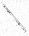
- Fig. 1 shows a perspective sketch of a lamp 3 according to the application.
- the lamp 3 can in particular - as shown - be an elongated lamp which extends along a longitudinal axis L.
- the luminaire 3 can be a so-called beam luminaire which is provided for producing a so-called light band and which is designed to be mechanically and electrically connected to a mounting rail (not shown in the figures).
- the lamp 3 has a so-called rotary tap 31 for this purpose.
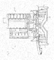
- Fig. 2 shows a cross-sectional sketch normal to the longitudinal axis L.
- the lamp has a circuit board 1 with at least one LED 2 arranged thereon, also referred to here briefly as “LED circuit board”.
- LED circuit board also referred to here briefly as “LED circuit board”.
- Fig. 4 the circuit board 1 with the LED 2 arranged thereon is sketched in a corresponding cross section in a separate form.
- the circuit board 1 is preferably designed as a profile-like component, so that a profile axis P is defined, which is preferably oriented parallel to the longitudinal axis L.
- a plurality of LEDs 2 are preferably arranged on the circuit board 1, in particular along a row parallel to the longitudinal axis L or the profile axis P.
- the luminaire 3 can have an operating device 32, in particular in the form of a converter or driver, which is used to provide an electrical current for a power supply to the at least one LED 2.
- the circuit board 1 has a layer formed from a sheet metal.
- the layer has a first flat area 4 and a dimensionally stable curved area 5.
- dimensionally stable bent it should be expressed that the area 5 in question has an intended curved shape and is bent so intrinsically stable that this shape is maintained if no external force acts on it or only gravity.
- the curved area has an elastic behavior, so that after a deflecting force has ended, the intended curved shape is automatically assumed again.
- the design is preferably such that the circuit board 1 mainly consists of the layer.
- the position can form a shape-forming framework, particularly preferably the only shape-forming framework of the circuit board 1.
- the circuit board 1 should consist of the layer and at least one layer arranged thereon, which serves to form a conductor track of the circuit board and represents a lacquer layer. This will be discussed in more detail below.
- the mechanical stability of the position is selected in such a way that the circuit board 1 is the supporting component of the lamp 3, in particular the housing of the Luminaire 3, or luminaire housing for short, is suitable.
- the flat area 4 is also designed to be correspondingly stable.
- a housing of the lamp 3 is formed by the circuit board 1.
- the layer consists of an aluminum sheet or a steel sheet or a copper sheet.
- the thickness of the layer is at least 0.5 mm, particularly preferably at least 1 mm.
- the bent region 5 is preferably bent about a bending axis oriented parallel to the profile axis P.
- the design is such that the location is configured to form the first flat area 4 and the curved area 5 in a coherent form.
- the curved area 5 preferably has a radius of curvature which is less than 10 mm, particularly preferably less than 5 mm, the curved area 5 being designed in particular in such a way that - as exemplarily in FIG Fig. 4 outlined - an edge is formed.
- the layer preferably also has a second planar region 6, which is arranged opposite the first planar region 4 with respect to the curved region 5.
- the second flat area 6 is preferably the same size or smaller than the first flat area 4, but at least as large as 10%, particularly preferably 20%, of the first flat area 4 Fig. 1 emerges, in the example shown the second flat region 6 extends through a part of the circuit board 1 which forms an outer surface region of the lamp 3. This is advantageous because in this way a heat generated during the operation of the LED 2 can be released particularly effectively into a surrounding area or outside area of the lamp 3.
- the first flat region 4 and the second flat region 6 delimit an angle a which is approximately 90 °.
- the first flat area 4 and the second flat area 6 delimit an angle ⁇ which is greater than 40 ° and less than 140 °.
- one of the two flat areas, here the first flat area 4 can be used as a suitable area for the protected arrangement of the LED 2 and the other, here the second flat area 6, can be used to design an outer surface of the lamp, via which a particularly suitable heat emission is made possible .
- the layer preferably also has a further dimensionally stable curved region 7, which, with reference to the first flat region 4, is formed opposite the first dimensionally stable curved region 5.
- the at least one LED 2 is arranged on the first flat area 4. A protected area for LED 2 can thus be formed in a particularly suitable manner.
- the position is preferably viewed in a cross section normal to the profile axis P with reference to a - in Fig. 4 exemplary sketched - middle plane E at least substantially symmetrical, wherein preferably the at least one LED 2 is arranged lying on the middle plane E.
- This is advantageous with regard to the design of the circuit board 1 as a luminaire housing.
- the layer preferably also has a third planar region 9, which is formed opposite the first planar region 4, in particular with reference to the further dimensionally stable region 7.
- the design can advantageously be such that the first planar region 4, the second planar region 6 and the third planar region 9 are U-shaped when viewed in a cross section normal to the longitudinal axis L or profile axis P. is formed with two U-legs and a connecting leg connecting the two U-legs to each other, the two U-legs being formed by the second planar region 6 and the third planar region 9 and by the first planar region 4 the connecting leg.
- a particularly suitable protected inner region 10 for arranging the LED 2 can be formed by the circuit board 1 and two opposite outer regions of the luminaire by the two U-legs for a particularly effective heat emission.
- the third flat area 9 can be designed symmetrically with respect to the central plane E to the second flat area 6.
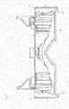
- the luminaire in the example shown further has a light influencing element 8 for influencing a light emitted by the at least one LED 2.
- the light influencing element 8 is arranged held on the circuit board 1.
- the circuit board 1 is preferably designed in such a way that it has holding elements 11, 12 which are designed to hold the light influencing element 8, in particular in the form of latching elements for producing a latching connection, by means of which the light influencing element 8 is held on the circuit board 1.
- the LED circuit board with the light influencing element 8 held thereon is outlined.
- the holding elements 11, 12 - as sketched - can be designed such that they each have a V-shaped cross section.
- the light influencing element 8 can have two corresponding latching lugs 81, 82.
- This design enables a particularly simple assembly of the light influencing element 8 on the circuit board 1.
- the holding elements 11, 12 can advantageously be formed by continuations of the second flat area 6 and the third flat area 9.
- the first flat region 4 of the circuit board 1 extends through a circuit board region which has two opposite surface regions, a first surface region 13 and a second surface region 14, the at least one LED 2 being arranged on the first surface region 13.
- the lamp 3 is intended to be aligned for operation in such a way that the first surface area 13 points downward and the second surface area 14 points upward.
- the design is such that the luminaire 3 emits the light generated by the LED 2 downwards. Accordingly, the lamp 3 is particularly suitable as a ceiling lamp.
- the two U-legs also point downward in this orientation of the circuit board 1.
- the lamp 3 can also be designed such that the operating device 32 with reference to the first planar area 4 of which at least one LED 2 is arranged opposite one another, in particular on the second surface area 14 of the circuit board 1, that is to say in the orientation considered here on the “upper side” of the circuit board area through which the first plane area 4 of the layer extends.
- the rotary tap 31 can also be arranged on the second surface area 14.
- the luminaire 3 can have, for example, a cable holder 33 and / or a connection terminal for a cable on the second surface area 14, which is provided, for example, for supplying power to the LED 2.
- the lamp mainly consists of the board 1.
- the circuit board 1 can be designed in such a way that it has two connection structures 15, 16 which are provided for holding the lamp 3 on the above-mentioned mounting rail.
- end parts of the board 1 are arranged or are arranged on the two end regions of the board 1 which are defined by the profile axis P.
- the circuit board 1 thus represents an integral part of a load-bearing part of the lamp 3 or a housing of the lamp 3.
- the circuit board 1 is designed in such a way that it has profiled areas on two opposite sides, which on the one hand attach to the mounting rail serve and on the other hand to hold the light influencing element 8.
- the profiled areas of the circuit board 1 thus comprise on the one hand the connecting structures 15, 16 for holding the lamp 3 on the mounting rail and on the other hand the holding elements 11, 12 for generating the snap-in connection for holding the light influencing element 8.
- the profiled areas are preferably each formed by a plurality of bends in the layer, each of which is bent about bending axes oriented parallel to the profile axis P.
- a method for producing the circuit board 1 is preferably provided, which has the following steps: a) Unwinding a semi-finished product, wound on a roll, which has a layer of metal formed from a sheet, in particular from an aluminum sheet, a steel sheet or a copper sheet, b) creating a dimensionally stable bent region 5 of the layer by bending the semi-finished product, c) cutting the semi-finished product to form a profile element and d) attaching at least one LED 2 to a surface 13 of the profile element.
- the following sequence is particularly provided: a), b), c), d).
- the semi-finished product wound on a roll can be provided in the form of a coil.
- a sheet can be provided as a semi-finished product that has a lacquer layer, for example a one-sided lacquer layer or both-sided lacquer layers.
- the lacquer layer or one of the two lacquer layers can advantageously serve to form an outer surface of the lamp 3. This is particularly advantageous with regard to effective heat emission or heat radiation to the environment.
- it can advantageously be used as a dielectric for forming a conductor track of the circuit board 1.
- the coil is unwound and treated or machined horizontally in a production line to produce the luminaire housing, in particular by stamping and / or embossing and / or the formation of beads and / or rollers.
- the stability and the desired, intended shape of the circuit board 1 described above can be generated in a particularly suitable manner.
- the semi-finished product treated in this way is cut off, so that profile elements are formed which represent, so to speak, "luminaire pieces".
- the method preferably also has the following step: e) forming a conductor track of the circuit board 1, step e) either taking place before step a) or between steps a) and b) or between steps b) and d).
- step d) the LED 2 is also electrically connected to the conductor track, in particular using a soldering furnace. It can be provided that the "luminaire pieces" formed by the cutting in step c) are fed to the soldering furnace in a batch process and are equipped with the at least one LED 2 there.
- a luminaire can be manufactured which comprises a method for producing the circuit board 1 according to the application. In this way, a particularly advantageous manufacturing method for the lamp 3 is made possible.
- the finished printed circuit boards can then be fed to a final assembly, in which the light influencing element 8, the operating device 32, the rotary tap 31, the cable holder 33, the end parts and / or the connecting terminal are optionally mounted.
- electrical connections can be made during final assembly.
- a circuit board film is laminated onto a shaped and cut semifinished product or a piece of lighting.
- the circuit board film can be designed in such a way that it forms a dielectric, the conductor track and a solder resist.
- a partial area of the circuit board 1, for example the second flat area 6 of the layer, is not provided with a conductor track.
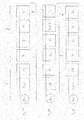
- FIG. 5 to 12 are shown sketches for possible processes in a method according to the application, which is not part of the invention.
- the rectangular boxes mean procedural steps, the chronological sequence from left to right being shown. The starting point is always - as symbolized by a circle, a metal coil.
- the arrows c shown above the boxes refer to a continuous process section, the arrows b to a process section in a batch operation.
- iron (III) chloride sodium sulfate or ammonium persulfate can be used in the etching bath.
- the cutting can be provided after assembly, for. B. with the help of a mobile soldering furnace or a clocked production line.
Landscapes
- Engineering & Computer Science (AREA)
- General Engineering & Computer Science (AREA)
- Microelectronics & Electronic Packaging (AREA)
- Architecture (AREA)
- Manufacturing & Machinery (AREA)
- Physics & Mathematics (AREA)
- Optics & Photonics (AREA)
- Fastening Of Light Sources Or Lamp Holders (AREA)
- Arrangement Of Elements, Cooling, Sealing, Or The Like Of Lighting Devices (AREA)
- Insulated Metal Substrates For Printed Circuits (AREA)
- Electroluminescent Light Sources (AREA)
- Non-Portable Lighting Devices Or Systems Thereof (AREA)
Description
- Die Erfindung betrifft eine Leuchte mit einer LED-Platine (LED: Licht emittierende Diode). Mit "Platine" sei hierbei ein Träger einer elektronischen Schaltung bezeichnet und mit "LED-Platine" eine Platine mit wenigstens einer darauf angeordneten LED.
- Aus dem Stand der Technik ist es bekannt, Platinen in einem Batch-Prozess zu fertigen. Das Trägermaterial ("Nutzen") wird hierbei beschichtet, bestückt und zugeschnitten. So genannte "Endlosplatinen" (Flexstripes) werden in einem Batch-Prozess auf Folien gefertigt, zugeschnitten, an den Enden zusammengelötet, und aufgerollt zu "Endlosplatinen". Eine Beschränkung ist hierbei zum einen durch die Länge der Nutzen (600 mm) gegeben und zum anderen durch die Anlagengröße (Batch-Reaktor). Allgemein ist die Herstellung vergleichsweise kosten- und zeitintensiv.
- Aus dem Stand der Technik ist weiterhin eine Leuchte mit einer LED-Platine bekannt, bei der die wenigstens eine LED eine Lichtquelle der Leuchte bildet. Die Leuchte weist ein Leuchtengehäuse auf, wobei die LED-Platine gut Wärme leitend an dem Leuchtengehäuse befestigt ist. Die Wärme leitende Verbindung ist dabei wichtig, weil bei Betrieb der Leuchte durch die LED Wärme erzeugt wird, die abtransportiert werden soll, um geeignete Betriebsbedingungen für die LED zu gewährleisten.
- Zur Herstellung der Leuchte muss dementsprechend in einem Verfahrensschritt die LED-Platine gut Wärme leitend an dem Leuchtengehäuse befestigt werden. Dieser Verfahrensschritt erfordert einen signifikanten Aufwand.
- Aus der
DE 20 2014 104 797 U1 ist eine Leuchte mit einem Trägerelement bekannt, auf dem eine LED-Lichtquelle angeordnet ist. Das Trägerelement besteht aus einem gebogenen Blechteil. - Aus der
DE 20 2016 000 122 U1 ist eine Feuchtraumleuchte mit einem, aus einer Blechplatte gebildeten Träger bekannt, auf dem Halbleiterlichtquellen in einem Modul mit Platine angebracht sind. - Ferner ist aus der
DE 10 2009 054 840 A1 bekannt, eine LED-Platine formbeständig in eine von einer planaren Form abweichende profilierte Form zu biegen. - Der Erfindung liegt die Aufgabe zugrunde, eine Leuchte mit einer verbesserten LED-Platine anzugeben.
- Insbesondere soll mit der LED-Platine bei guten thermischen Eigenschaften eine einfache Herstellung der Leuchte ermöglicht sein.
- Diese Aufgabe wird gemäß der Erfindung mit dem in Anspruch 1 genannten Gegenstand gelöst. Besondere Ausführungsarten der Erfindung sind in den abhängigen Ansprüchen angegeben.
- Gemäß der Erfindung wird eine Leuchte mit einer Platine mit wenigstens einer darauf angeordneten LED sowie einem Lichtbeeinflussungselement zur Beeinflussung eines von der wenigstens einen LED abgestrahlten Lichts vorgeschlagen,
wobei die Platine eine, aus einem Blech gebildete Lage aufweist, insbesondere aus einem Aluminiumblech, einem Stahlblech oder einem Kupferblech,
wobei die Lage einen ersten planen Bereich und einen formbeständig gebogenen Bereich aufweist,
wobei die Platine aus der Lage und wenigstens einer darauf angeordneten Schicht besteht, die zur Bildung einer Leiterbahn der Platine dient und eine Lackschicht darstellt,
und wobei die Platine derart ausgeführt ist, dass sie auf zwei gegenüberliegenden Seiten profilierte Bereiche aufweist, die einerseits der Befestigung an einer Tragschiene dienen und andererseits der Halterung des Lichtbeeinflussungselements, so dass das Lichtbeeinflussungselement an der Platine gehalten angeordnet ist. - Durch die Verwendung der Lage aus Blech ist eine besonders geeignete Herstellung der Platine ermöglicht. Beispielsweise kann hierzu ein so genanntes "Coil" bzw. "Metall-Coil", also eine Metallblechrolle, beispielsweise eine Bandstahlrolle verwendet werden; durch Abwickeln des Coils lässt sich besonders geeignet ein kontinuierlicher Herstellungsschritt realisieren. Das Coil kann hierzu beispielsweise einfach auf einer Haspel aufgespannt und dann abgerollt werden.
- Dabei eignet sich die Platine durch den formbeständig gebogenen Bereich erfindungsgemäß als ein tragendes Teil der Leuchte, beispielsweise als ein Gehäuse der Leuchte. Der plane Bereich eignet sich besonders zur Verbindung mit der LED. Zudem ist durch diese Gestaltung eine besonders effektive Wärmeableitung einer von der LED erzeugten Wärme ermöglicht. Die Platine kann somit besonders geeignet als Kühlkörper der Leuchte bzw. für die LED dienen.
- Erfindungsgemäß besteht die Platine aus der Lage und wenigstens einer darauf angeordneten Schicht, die zur Bildung einer Leiterbahn der Platine dient und eine Lackschicht darstellt.
- Vorzugsweise ist dabei die Lage den ersten planen Bereich und den gebogenen Bereich in zusammenhängender Form bildend ausgestaltet. Hierdurch sind insbesondere eine gute Formstabilität und eine gute Ableitung einer durch die LED erzeugten Wärme ermöglicht.
- Vorzugsweise weist der gebogene Bereich einen Krümmungsradius auf, der kleiner als 10 mm ist, vorzugsweise kleiner als 5 mm, wobei der gebogene Bereich insbesondere derart gestaltet ist, dass durch ihn eine Kante gebildet ist. Hierdurch lässt sich besonders geeignet eine gute Stabilität der Platine erzielen. Außerdem ist diese Gestaltung zum Beispiel vorteilhaft mit Bezug auf die Eignung der Platine als Leuchtengehäuse.
- Vorzugsweise weist die Lage weiterhin einen zweiten planen Bereich auf, der mit Bezug auf den gebogenen Bereich dem ersten planen Bereich gegenüberliegend angeordnet ist, wobei der zweite plane Bereich gleich groß wie oder kleiner als der erste plane Bereich ist, jedoch mindestens so groß ist wie 10%, vorzugsweise wie 20% des ersten planen Bereichs. Durch diese Gestaltung eignet sich die Platine besonders als Gehäuse der Leuchte. Vorzugsweise begrenzen dabei der erste plane Bereich und der zweite plane Bereich einen Winkel, der größer als 40° und kleiner als 140° ist.
- Vorzugsweise bildet die Platine zumindest im Wesentlichen ein profilförmiges Bauteil, durch das eine Profilachse festgelegt ist, wobei der gebogene Bereich um eine parallel zu der Profilachse orientiert Biegeachse gebogen ist. Hierdurch eignet sich die Platine insbesondere als Leuchtengehäuse einer länglichen Leuchte, beispielsweise einer so genannten "Lichtbandleuchte".
- Vorzugsweise weist die Lage dabei außerdem einen weiteren formbeständig gebogenen Bereich auf, der mit Bezug auf den ersten planen Bereich dem zuerst genannten formbeständig gebogenen Bereich gegenüberliegend ausgebildet ist, wobei die wenigstens eine LED auf dem ersten planen Bereich angeordnet ist. Auf diese Weise lässt sich die Platine insbesondere besonders geeignet als schützendes Element der wenigstens einen LED gestalten.
- Vorzugsweise ist dabei die Lage in einem Querschnitt normal zu der Profilachse betrachtet mit Bezug auf eine Mittelebene zumindest im Wesentlichen symmetrisch gestaltet, wobei vorzugsweise die wenigstens eine LED auf der Mittelebene liegend angeordnet ist. So eignet sich die Platine besonders als symmetrisches Leuchtengehäuse, durch das besonders geeignet eine Wärmeableitung auf zwei gegenüberliegende Seiten ermöglicht ist.
- Vorzugsweise ist dabei durch einen Oberflächenbereich der Platine ein Außenflächenbereich der Leuchte gebildet. Dies ist insbesondere vorteilhaft mit Bezug auf gute thermische Eigenschaften der Leuchte zur Ableitung von Wärme, die bei Betrieb der Leuchte durch die wenigstens eine LED erzeugt wird.
- Vorzugsweise ist dabei durch die Platine ein Gehäuse der Leuchte gebildet. So lässt sich eine besonders effektive Wärmeabgabe an die Umgebung der Leuchte erzielen. Außerdem ist hierdurch die Herstellung grundsätzlich erleichtert, da anstelle von zwei unterschiedlichen Bauteilen, nämlich Gehäuse und LED-Platine, lediglich ein Bauteil, nämlich die anmeldungsgemäße LED-Platine hergestellt werden muss.
- Die Erfindung wird im Folgenden anhand eines Ausführungsbeispiels und mit Bezug auf die Zeichnungen näher erläutert. Es zeigen:
- Fig. 1
- eine perspektivische Skizze einer anmeldungsgemäßen Leuchte mit einer anmeldungsgemäßen LED-Platine,
- Fig. 2
- eine Querschnitt-Skizze der Leuchte,
- Fig. 3
- eine entsprechende Querschnittskizze der LED-Platine und eines daran gehaltenen Lichtbeeinflussungselements,
- Fig. 4
- eine entsprechende Querschnitt-Skizze der separierten LED-Platine und
- Figuren 5 bis 12
- Skizzen zu Abläufen eines anmeldungsgemäßen Verfahrens zur Herstellung der Platine.
-
Fig. 1 zeigt eine perspektivische Skizze einer anmeldungsgemäßen Leuchte 3. Bei der Leuchte 3 kann es sich insbesondere - wie gezeigt - um eine längliche Leuchte handeln, die sich entlang einer Längsachse L erstreckt. Insbesondere kann es sich bei der Leuchte 3 um eine so genannte Balkenleuchte handeln, die zur Erzeugung eines so genannten Lichtbands vorgesehen ist und die dazu ausgestaltet ist, mechanisch und elektrisch mit einer (in den Figuren nicht gezeigten) Tragschiene verbunden zu werden. Bei dem inFig. 1 gezeigten Beispiel weist die Leuchte 3 hierfür einen so genannten Rotationsabgriff 31 auf. -
Fig. 2 zeigt eine Querschnitt-Skizze normal zu der Längsachse L. Die Leuchte weist eine Platine 1 mit wenigstens einer darauf angeordneten LED 2 auf, hier auch kurz als "LED-Platine" bezeichnet. InFig. 4 ist die Platine 1 mit der darauf angeordneten LED 2 in separierter Form in einem entsprechenden Querschnitt skizziert. - Vorzugsweise ist die Platine 1 als profilartiges Bauteil gestaltet, so dass eine Profilachse P festgelegt ist, die vorzugsweise parallel zu der Längsachse L orientiert ist. Vorzugsweise sind mehrere LEDs 2 auf der Platine 1 angeordnet, insbesondere entlang einer zu der Längsachse L bzw. der Profilachse P parallelen Reihe. Außerdem kann die Leuchte 3 ein Betriebsgerät 32, insbesondere in Form eines Konverters oder Treibers aufweisen, das zur Bereitstellung eines elektrischen Stroms für eine Stromversorgung der wenigstens eine LED 2 dient.
- Die Platine 1 weist eine, aus einem Blech gebildete Lage auf. Die Lage weist dabei einen ersten planen Bereich 4 und einen formbeständig gebogenen Bereich 5 auf. Mit "formbeständig gebogen" sei dabei zum Ausdruck gebracht, dass der betreffende Bereich 5 eine vorgesehene gebogene Form aufweist und dabei derart eigenstabil gebogen ist, dass diese Form beibehalten wird, wenn keine äußere Kraft auf ihn einwirkt bzw. lediglich die Schwerkraft. Insbesondere weist der gebogene Bereich ein elastisches Verhalten auf, so dass nach Beendigung einer auslenkenden Kraft die vorgesehene gebogene Form wieder selbstständig eingenommen wird.
- Vorzugsweise ist die Gestaltung derart, dass die Platine 1 überwiegend aus der Lage besteht. Insbesondere kann durch die Lage ein formbildendes Gerüst, besonders bevorzugt das einzige formbildende Gerüst der Platine 1 gebildet sein. Die Platine 1 soll aus der Lage und wenigstens einer darauf angeordneter Schicht bestehen, die zur Bildung einer Leiterbahn der Platine dient und eine Lackschicht darstellt. Hierauf wird im Folgenden noch genauer eingegangen.
- Insbesondere ist die mechanische Stabilität der Lage derart gewählt, dass sich dadurch die Platine 1 als tragendes Bauteil der Leuchte 3, insbesondere als Gehäuse der Leuchte 3, kurz Leuchtengehäuse, eignet. Insbesondere ist auch der plane Bereich 4 entsprechend stabil gestaltet. Beim gezeigten Beispiel ist durch die Platine 1 ein Gehäuse der Leuchte 3 gebildet.
- Beispielsweise kann vorgesehen sein, dass die Lage aus einem Aluminiumblech oder einem Stahlblech oder einem Kupferblech besteht. Beispielsweise kann vorgesehen sein, dass die Dicke der Lage wenigsten 0,5 mm beträgt, besonders bevorzugt wenigstens 1 mm.
- Vorzugsweise ist der gebogene Bereich 5 - wie im gezeigten Beispiel der Fall - um eine parallel zu der Profilachse P orientierte Biegeachse gebogen.
- Insbesondere ist die Gestaltung derart, dass die Lage den ersten planen Bereich 4 und den gebogenen Bereich 5 in zusammenhängender Form bildend ausgestaltet ist.
- Vorzugsweise weist der gebogene Bereich 5 einen Krümmungsradius auf, der kleiner als 10 mm ist, besonders bevorzugt kleiner als 5 mm, wobei der gebogene Bereich 5 insbesondere derart gestaltet ist, dass durch ihn - wie beispielhaft in
Fig. 4 skizziert - eine Kante gebildet ist. - Wie beim gezeigten Beispiel der Fall, weist die Lage vorzugsweise außerdem einen zweiten planen Bereich 6 auf, der mit Bezug auf den gebogenen Bereich 5 dem ersten planen Bereich 4 gegenüberliegend angeordnet ist. Dabei ist der zweite plane Bereich 6 vorzugsweise gleich groß oder kleiner als der erste plane Bereich 4, jedoch mindestens so groß wie 10%, besonders bevorzugt 20% des ersten planen Bereichs 4. Wie beispielsweise aus
Fig. 1 hervorgeht, erstreckt sich beim gezeigten Beispiel der zweite plane Bereich 6 durch einen Teil der Platine 1, der einen Außenflächenbereich der Leuchte 3 bildet. Das ist vorteilhaft, weil hierdurch eine, beim Betrieb der LED 2 erzeugte Wärme besonders effektiv in einen Umgebungsbereich bzw. Außenbereich der Leuchte 3 abgegeben werden kann. - Wie in
Fig. 4 angedeutet, begrenzen beim gezeigten Beispiel der erste plane Bereich 4 und der zweite plane Bereich 6 einen Winkel a, der etwa 90° beträgt. Allgemein ist vorzugsweise vorgesehen, dass dass der erste plane Bereich 4 und der zweite plane Bereich 6 einen Winkel α begrenzen, der größer als 40° und kleiner als 140° ist. So lässt sich einer der beiden planen Bereiche, hier der erste plane Bereich 4 als geeigneter Bereich zur geschützten Anordnung der LED 2 nutzen und der andere, hier der zweite plane Bereich 6 zur Gestaltung einer Außenfläche der Leuchte, über die eine besonders geeignete Wärmeabgabe ermöglicht ist. - Außerdem weist die Lage weiterhin vorzugsweise einen weiteren formbeständig gebogenen Bereich 7 auf, der mit Bezug auf den ersten planen Bereich 4 dem zuerst genannten formbeständig gebogenen Bereich 5 gegenüberliegend ausgebildet ist. Dabei ist die wenigstens eine LED 2 auf dem ersten planen Bereich 4 angeordnet. So lässt sich besonders geeignet ein geschützter Bereich für die LED 2 bilden.
- Weiterhin vorzugsweise ist die Lage in einem Querschnitt normal zu der Profilachse P betrachtet mit Bezug auf eine - in
Fig. 4 beispielhaft skizzierte - Mittelebene E zumindest im Wesentlichen symmetrisch gestaltet, wobei vorzugsweise die wenigstens eine LED 2 auf der Mittelebene E liegend angeordnet ist. Dies ist vorteilhaft mit Bezug auf die Gestaltung der Platine 1 als Leuchtengehäuse. - Weiterhin vorzugsweise weist die Lage außerdem einen dritten planen Bereich 9 auf, der insbesondere mit Bezug auf den weiteren formbeständig gebogenen Bereich 7 dem ersten planen Bereich 4 gegenüberliegend ausgebildet ist. Wie beim gezeigten Beispiel der Fall, kann die Gestaltung hierbei vorteilhaft derart sein, dass durch den ersten planen Bereich 4, den zweiten planen Bereich 6 und den dritten planen Bereich 9 in einem Querschnitt normal zu der Längsachse L oder Profilachse P betrachtet eine U-Form mit zwei U-Schenkeln und einem, die beiden U-Schenkel miteinander verbindenden Verbindungsschenkel gebildet ist, wobei durch den zweiten planen Bereich 6 und den dritten planen Bereich 9 die zwei U-Schenkel gebildet sind und durch den ersten planen Bereich 4 der Verbindungschenkel. So lässt sich durch die Platine 1 ein besonders geeigneter geschützter Innenbereich 10 zur Anordnung der LED 2 bilden und durch die beiden U-Schenkel zwei gegenüberliegende Außenbereiche der Leuchte für eine besonders effektive Wärmeabgabe. Beispielsweise lässt sich der dritte plane Bereich 9 mit Bezug auf die Mittelebene E symmetrisch zu dem zweiten planen Bereich 6 gestalten.
- Wie beispielsweise aus
Fig. 2 hervorgeht, weist die Leuchte beim gezeigten Beispiel weiterhin ein Lichtbeeinflussungselement 8 zur Beeinflussung eines von der wenigstens einen LED 2 abgestrahlten Lichts auf. Dabei ist das Lichtbeeinflussungselement 8 an der Platine 1 gehalten angeordnet. Vorzugsweise ist hierzu die Platine 1 derart gestaltet, dass sie Halteelemente 11, 12 aufweist, die zum Halten des Lichtbeeinflussungselements 8 ausgestaltet sind, insbesondere in Form von Rastelementen zur Erzeugung einer Rastverbindung, durch die das Lichtbeeinflussungselement 8 an der Platine 1 gehalten ist. InFig. 3 ist die LED-Platine mit dem daran gehaltenen Lichtbeeinflussungselement 8 skizziert. Beispielsweise können die Halteelemente 11, 12 - wie skizziert - derart gestaltet sein, dass sie jeweils einen V-förmigen Querschnitt aufweisen. Das Lichtbeeinflussungselement 8 kann hierzu zwei entsprechende Rastnasen 81, 82 aufweisen. Durch diese Gestaltung ist eine besonders einfache Montage des Lichtbeeinflussungselements 8 an der Platine 1 ermöglicht. Vorteilhaft können die Halteelemente 11, 12 durch Fortsetzungen des zweiten planen Bereichs 6 und des dritten planen Bereichs 9 gebildet sein. - Beim gezeigten Beispiel erstreckt sich der erste plane Bereich 4 der Platine 1 durch einen Platinen-Bereich, der zwei gegenüberliegende Oberflächenbereiche aufweist, einen ersten Oberflächenbereich 13 und einen zweiten Oberflächenbereich 14, wobei die wenigstens eine LED 2 auf dem ersten Oberflächenbereich 13 angeordnet ist. Beim gezeigten Beispiel ist die Leuchte 3 dafür vorgesehen, zum Betrieb derart ausgerichtet zu werden, dass der erste Oberflächenbereich 13 nach unten weist und der zweite Oberflächenbereich 14 nach oben. Dabei ist die Gestaltung derart, dass die Leuchte 3 das von der LED 2 erzeugte Licht nach unten abgibt. Die Leuchte 3 eignet sich dementsprechend insbesondere als Deckenleuchte. Auch die beiden U-Schenkel weisen bei dieser Ausrichtung der Platine 1 nach unten.
- Wie aus
Fig. 1 in Verbindung mitFig. 2 hervorgeht, kann die Leuchte 3 weiterhin derart gestaltet sein, dass das Betriebsgerät 32 mit Bezug auf den ersten planen Bereich 4 der wenigstens einen LED 2 gegenüberliegend angeordnet ist, insbesondere auf dem zweiten Oberflächenbereich 14 der Platine 1, also bei der hier betrachteten Ausrichtung auf der "Oberseite" des Platinen-Bereichs, durch den sich der erste plane Bereich 4 der Lage erstreckt. Auch der Rotationsabgriff 31 kann auf dem zweiten Oberflächenbereich 14 angeordnet sein. Weiterhin kann die Leuchte 3 auf dem zweiten Oberflächenbereich 14 beispielsweise einen Kabelhalter 33 und/oder eine Anschlussklemme für ein Kabel aufweisen, das beispielsweise zur Stromversorgung der LED 2 vorgesehen ist. - Wie aus
Fig. 1 zu erkennen, besteht die Leuchte überwiegend aus der Platine 1. - Weiterhin kann die Platine 1 derart gestaltet sein, dass sie zwei Verbindungsstrukturen 15, 16 aufweist, die zur Halterung der Leuchte 3 an der oben erwähnten Tragschiene vorgesehen sind.
- Weiterhin kann vorgesehen sein, dass an den beiden, durch die Profilachse P festgelegten Endbereichen der Platine 1 (in den Figuren nicht gezeigte) Stirnteile angeordnet sind bzw. werden.
- Im gezeigten Beispiel stellt die Platine 1 mithin einen integralen Bestandteil eines tragenden Teils der Leuchte 3 bzw. eines Gehäuses der Leuchte 3 dar. Die Platine 1 ist derart ausgeführt, dass sie auf zwei gegenüberliegenden Seiten profilierte Bereiche aufweist, die einerseits der Befestigung an der Tragschiene dienen und andererseits der Halterung des Lichtbeeinflussungselements 8. Die profilierten Bereiche der Platine 1 umfassen also zum einen die Verbindungsstrukturen 15, 16 zur Halterung der Leuchte 3 an der Tragschiene und zum anderen die Halteelemente 11, 12 zur Erzeugung der Rastverbindung zur Halterung des Lichtbeeinflussungselements 8. Die profilierten Bereiche sind dabei vorzugsweise jeweils durch mehrere Biegungen der Lage gebildet, die jeweils um parallel zur Profilachse P orientierte Biegeachsen gebogen sind.
- Zur Herstellung der Platine 1 ist vorzugsweise ein Verfahren vorgesehen, das die folgenden Schritte aufweist: a) Abwickeln eines, auf einer Rolle aufgewickelten Halbzeugs, das eine aus einem Blech gebildete Lage aus Metall aufweist, insbesondere aus einem Aluminiumblech, einem Stahlblech oder einem Kupferblech, b) Erzeugen eines formbeständig gebogenen Bereichs 5 der Lage durch ein Biegen des Halbzeugs, c) Schneiden des Halbzeugs zur Bildung eines Profilelements und d) Befestigen wenigstens einer LED 2 auf einer Oberfläche 13 des Profilelements. Dabei ist insbesondere die folgende Reihenfolge vorgesehen: a), b), c), d).
- Im Schritt a) kann insbesondere das auf einer Rolle aufgewickelte Halbzeug in Form eines Coils vorgesehen sein. Als Halbzeug kann dabei insbesondere ein Blech vorgesehen sein, das eine Lackschicht aufweist, zum Beispiel eine einseitige Lackschicht oder beidseitige Lackschichten. Die Lackschicht bzw. eine der beiden Lackschichten kann dabei vorteilhaft zur Bildung einer Außenfläche der Leuchte 3 dienen. Dies ist insbesondere vorteilhaft mit Bezug auf eine effektive Wärmeabgabe bzw. Wärmeabstrahlung an die Umgebung. Außerdem kann sie vorteilhaft als Dielektrikum zur Bildung einer Leiterbahn der Platine 1 verwendet werden.
- Weiterhin kann vorteilhaft vorgesehen sein, dass das Coil abgerollt wird und in der Horizontalen in einer Fertigungsstraße zur Erzeugung des Leuchtengehäuses behandelt bzw. bearbeitet wird, insbesondere durch Stanzen und/oder Prägen und/oder das Bilden von Sicken und/oder Walzen. So lässt sich besonders geeignet die Stabilität und die oben beschriebene gewünschte, vorgesehene Form der Platine 1 erzeugen. Im Weiteren kann vorgesehen sein, dass das so behandelte Halbzeug abgeschnitten wird, so dass Profilelemente gebildet werden, die sozusagen "Leuchtenstücke" darstellen.
- Vorzugsweise weist das Verfahren außerdem den folgenden Schritt auf: e) Bilden einer Leiterbahn der Platine 1, wobei der Schritt e) entweder vor dem Schritt a) erfolgt oder zwischen den Schritten a) und b) oder zwischen den Schritten b) und d). Dabei wird im Schritt d) die LED 2 außerdem elektrisch mit der Leiterbahn verbunden, insbesondere unter Nutzung eines Lötofens. Dabei kann vorgesehen sein, dass die durch das im Schritt c) erfolgte Schneiden gebildeten "Leuchtenstücke" in einem Batch-Prozess dem Lötofen zugeführt und dort mit der wenigstens einen LED 2 bestückt werden.
- Selbstverständlich kann eine Herstellung einer Leuchte vorgesehen sein, die ein anmeldungsgemäßes Verfahren zur Herstellung der Platine 1 umfasst. Auf diese Weise ist ein besonders vorteilhaftes Herstellungsverfahren für die Leuchte 3 ermöglicht.
- Die fertig bestückten Platinen können dabei anschließend einer Endmontage zugeführt werden, in der gegebenenfalls das Lichtbeeinflussungselement 8, das Betriebsgerät 32, der Rotationsabgriff 31, der Kabelhalter 33, die Stirnteile und/oder die Anschlussklemme montiert werden. Außerdem können im Rahmen der Endmontage elektrische Verbindungen gesteckt werden.
- Beispielsweise kann zur Bildung der Leiterbahn vorgesehen sein, dass auf ein geformtes und abgeschnittenes Halbzeug bzw. ein Leuchtenstück eine Platinenfolie auflaminiert wird. Die Platinenfolie kann derart gestaltet sein, dass sie ein Dielektrikum, die Leiterbahn und einen Lötstopplack ausbildet.
- Es kann vorgesehen sein, dass ein Teilbereich der Platine 1, beispielsweise der zweite plane Bereich 6 der Lage nicht mit einer Leiterbahn versehen wird.
- In den
Figuren 5 bis 12 sind Skizzen zu möglichen Abläufen bei einem anmeldungsgemäßen Verfahren, das nicht Teil der Erfindung ist, gezeigt. Dabei bedeuten die rechteckigen Kästchen Verfahrensschritte, wobei die zeitliche Abfolge von links nach rechts gezeigt ist. Ausgangspunkt ist jeweils - wie durch einen Kreis symbolisiert ein Metall-Coil. Die über den Kästchen gezeigten Pfeile c verweisen auf einen kontinuierlichen Prozessabschnitt, die Pfeile b auf einen Prozessabschnitt in einem Batch-Betrieb. - Die in den Kreisen bzw. Kästchen angegebenen Buchstaben bzw. Buchstabenkombinationen haben dabei folgende Bedeutung:
- M1: Metall-Coil, ein- oder beidseitig vorlackiert
- M2: Metall-Coil, komplett vorkonfektioniert
- M3: Metall-Coil, mit Metall - Dielektrikum - homogene Kupferschicht, Rückseite evtl. vorlackiert
- M4: Metall-Coil, mit ein- oder beidseitig auflaminierter Folie
- S: Stanzen / Prägen
- W: Walzen / Profilieren
- X: Schneiden
- LF: Auflaminierung: Flexplatine (unbestückte Leiterbahnen inklusive Dielektrikum und Lötstopplack)
- B: Bestückung im Lötofen
- F: Leuchtenfertigung
- LV: Auflaminieren vorkonfektionierte Leiterbahnfolie
- P: Fotolack Layout, z. B. Siebdruck Walze
- G: Belichtung, Ätzbad
- K: Lötstopplack
- LD: Auflaminieren zweier Folien: Dielektrikum und Kupfer oder einer Verbundfolie, z. B. Polyamid / Kupfer (Polyamid größer als Kupfer)
- Bei dem Ätzbad kann dabei beispielsweise Eisen(III)-chlorid, Natriumsulfat oder Ammoniumpersulfat verwendet werden.
- Darüber hinaus kann das Schneiden nach der Bestückung vorgesehen sein, z. B. mit Hilfe eines fahrbaren Lötofens oder einer getakteten Fertigungsstraße.
- Mit einer anmeldungsgemäßen LED-Platine bzw. einer anmeldungsgemäßen Leuchte bzw. einem anmeldungsgemäßen Verfahren lassen sich insbesondere die folgenden Vorteile erzielen:
- Die Platine bildet das Gehäuse der Leuchte.
- Das durch die Patine gebildete Gehäuse der Leuchte kann die betriebsbedingte, von der LED erzeugte Wärme besonders gut ableiten.
- Die Platine bildet Befestigungselemente aus, beispielsweise durch Stanzungen oder Sicken, an denen Leuchtenteile befestigt werden können, z. B. Anschlussklemmen, Treiber, Akkus, Stirnteile.
- Das Metall-Coil erlaubt eine besonders kostengünstige Herstellung der Leuchte.
- Im Unterschied zum bisherigen Stand der Technik fällt eine Platine als Extrateil und somit eine Befestigung derselben weg.
- Der Wärmeübergang von der LED zum Gehäuse lässt sich quasi ideal gestalten - reine Wärmeleitung innerhalb des Materials.
- Die Rückseite der Platine muss wegen der Anbindung zum Gehäuse nicht ideal glatt sein für einen guten Wärmeübergang.
- Lackierte Flächen des Gehäuses bzw. der Platine strahlen die Wärme gut ab.
- Die Platine kann als Kühlkörper fungieren.
- Es kann vorlackiertes Blech verwendet werden, so ist keine anschließende Lackierung bzw. Beschichtung notwendig.
Claims (8)
- Leuchte (3) mit einer Platine (1) mit wenigstens einer darauf angeordneten LED (2) sowie einem Lichtbeeinflussungselement (8) zur Beeinflussung eines von der wenigstens einen LED (2) abgestrahlten Lichts,
wobei die Platine (1) eine, aus einem Blech gebildete Lage aufweist, insbesondere aus einem Aluminiumblech, einem Stahlblech oder einem Kupferblech,
wobei die Lage einen ersten planen Bereich (4) und einen formbeständig gebogenen Bereich (5) aufweist,
wobei die Platine (1) aus der Lage und wenigstens einer darauf angeordneten Schicht besteht, die zur Bildung einer Leiterbahn der Platine (1) dient und eine Lackschicht darstellt,
und wobei die Platine (1) derart ausgeführt ist, dass sie auf zwei gegenüberliegenden Seiten profilierte Bereiche aufweist, die einerseits der Befestigung an einer Tragschiene dienen und andererseits der Halterung des Lichtbeeinflussungselements (8), so dass das Lichtbeeinflussungselement (8) an der Platine (1) gehalten angeordnet ist. - Leuchte nach Anspruch 1,
dadurch gekennzeichnet,
dass die Lage den ersten planen Bereich (4) und den gebogenen Bereich (5) in zusammenhängender Form bildend ausgestaltet ist. - Leuchte nach Anspruch 1 oder 2,
dadurch gekennzeichnet,
dass der gebogene Bereich (5) einen Krümmungsradius aufweist, der kleiner als 10 mm ist, vorzugsweise kleiner als 5 mm, wobei der gebogene Bereich (5) insbesondere derart gestaltet ist, dass durch ihn eine Kante gebildet ist. - Leuchte nach einem der vorhergehenden Ansprüche,
dadurch gekennzeichnet,
dass die Lage weiterhin einen zweiten planen Bereich (6) aufweist, der mit Bezug auf den gebogenen Bereich (5) dem ersten planen Bereich (4) gegenüberliegend angeordnet ist, wobei der zweite plane Bereich (6) gleich groß wie oder kleiner als der erste plane Bereich (4) ist, jedoch mindestens so groß ist wie 10%, vorzugsweise wie 20% des ersten planen Bereichs (4)
wobei vorzugsweise der erste plane Bereich (4) und der zweite plane Bereich (6) einen Winkel (α) begrenzen, der größer als 40° und kleiner als 140° ist. - Leuchte nach einem der vorhergehenden Ansprüche,
dadurch gekennzeichnet,
dass die Platine (1) zumindest im Wesentlichen ein profilförmiges Bauteil bildet, durch das eine Profilachse (P) festgelegt ist, wobei der gebogene Bereich (6) um eine parallel zu der Profilachse (P) orientiert Biegeachse gebogen ist
und wobei vorzugsweise die Lage weiterhin einen weiteren formbeständig gebogenen Bereich (7) aufweist, der mit Bezug auf den ersten planen Bereich (4) dem zuerst genannten formbeständig gebogenen Bereich (5) gegenüberliegend ausgebildet ist, wobei die wenigstens eine LED (2) auf dem ersten planen Bereich (4) angeordnet ist. - Leuchte nach Anspruch 5,
dadurch gekennzeichnet,
dass die Lage in einem Querschnitt normal zu der Profilachse (P) betrachtet mit Bezug auf eine Mittelebene (E) zumindest im Wesentlichen symmetrisch gestaltet ist, wobei vorzugsweise die wenigstens eine LED (2) auf der Mittelebene (E) liegend angeordnet ist. - Leuchte nach einem der vorherigen Ansprüche,
dadurch gekennzeichnet,
dass durch einen Oberflächenbereich der Platine (1) ein Außenflächenbereich der Leuchte gebildet ist. - Leuchte nach einem der vorherigen Ansprüche,
dadurch gekennzeichnet,
dass durch die Platine (1) ein Gehäuse der Leuchte gebildet ist.
Priority Applications (1)
| Application Number | Priority Date | Filing Date | Title |
|---|---|---|---|
| EP20172867.2A EP3708903B1 (de) | 2016-03-24 | 2017-03-24 | Led-platine für leuchte, herstellungsverfahren für eine solche led-platine sowie leuchte |
Applications Claiming Priority (1)
| Application Number | Priority Date | Filing Date | Title |
|---|---|---|---|
| DE102016204993.3A DE102016204993A1 (de) | 2016-03-24 | 2016-03-24 | LED-Platine für Leuchte, Herstellungsverfahren für eine solche LED-Platine sowie Leuchte |
Related Child Applications (1)
| Application Number | Title | Priority Date | Filing Date |
|---|---|---|---|
| EP20172867.2A Division EP3708903B1 (de) | 2016-03-24 | 2017-03-24 | Led-platine für leuchte, herstellungsverfahren für eine solche led-platine sowie leuchte |
Publications (3)
| Publication Number | Publication Date |
|---|---|
| EP3222902A2 EP3222902A2 (de) | 2017-09-27 |
| EP3222902A3 EP3222902A3 (de) | 2017-11-22 |
| EP3222902B1 true EP3222902B1 (de) | 2020-05-13 |
Family
ID=58428110
Family Applications (2)
| Application Number | Title | Priority Date | Filing Date |
|---|---|---|---|
| EP20172867.2A Active EP3708903B1 (de) | 2016-03-24 | 2017-03-24 | Led-platine für leuchte, herstellungsverfahren für eine solche led-platine sowie leuchte |
| EP17162727.6A Active EP3222902B1 (de) | 2016-03-24 | 2017-03-24 | Led-platine für leuchte, herstellungsverfahren für eine solche led-platine sowie leuchte |
Family Applications Before (1)
| Application Number | Title | Priority Date | Filing Date |
|---|---|---|---|
| EP20172867.2A Active EP3708903B1 (de) | 2016-03-24 | 2017-03-24 | Led-platine für leuchte, herstellungsverfahren für eine solche led-platine sowie leuchte |
Country Status (3)
| Country | Link |
|---|---|
| EP (2) | EP3708903B1 (de) |
| AT (1) | AT15970U1 (de) |
| DE (1) | DE102016204993A1 (de) |
Families Citing this family (2)
| Publication number | Priority date | Publication date | Assignee | Title |
|---|---|---|---|---|
| DE102017105722A1 (de) * | 2017-03-16 | 2018-09-20 | Siteco Beleuchtungstechnik Gmbh | LED-Leuchtenmodul mit flächigem Träger für LEDs |
| DE102017114235B4 (de) | 2017-06-27 | 2020-01-02 | Bjb Gmbh & Co. Kg | Leuchte für die Raum- und Gebäudebeleuchtung |
Citations (4)
| Publication number | Priority date | Publication date | Assignee | Title |
|---|---|---|---|---|
| GB2464668A (en) * | 2008-10-20 | 2010-04-28 | Sensitive Electronic Co Ltd | Thin light emitting diode circuit substrate and lamp strip |
| EP2280213A2 (de) * | 2009-07-28 | 2011-02-02 | LG Innotek Co., Ltd. | Beleuchtungsvorrichtung |
| DE102009054840A1 (de) * | 2009-12-17 | 2011-06-22 | Poly-Tech Service GmbH, 67681 | Leuchtmittel mit einer Mehrzahl von Leuchtdioden |
| DE102012108719A1 (de) * | 2012-09-17 | 2014-03-20 | Alanod Gmbh & Co. Kg | Reflektor, Beleuchtungskörper mit einem derartigen Reflektor und Verwendung eines Basismaterials zu dessen Herstellung |
Family Cites Families (7)
| Publication number | Priority date | Publication date | Assignee | Title |
|---|---|---|---|---|
| US3724068A (en) * | 1971-02-25 | 1973-04-03 | Du Pont | Semiconductor chip packaging apparatus and method |
| JP2587462B2 (ja) * | 1988-07-08 | 1997-03-05 | 株式会社フジクラ | ホウロウ基板及びその製造方法 |
| DE102009009288A1 (de) * | 2009-02-17 | 2010-08-26 | Osram Gesellschaft mit beschränkter Haftung | Starrflexible Trägerplatte |
| DE102013018549A1 (de) * | 2013-11-05 | 2015-05-07 | Siteco Beleuchtungstechnik Gmbh | Beleuchtungsvorrichtung |
| DE202014100258U1 (de) * | 2014-01-22 | 2015-04-24 | Zumtobel Lighting Gmbh | Leuchtensystem |
| DE202014104797U1 (de) * | 2014-10-07 | 2016-01-11 | Zumtobel Lighting Gmbh | Längliche LED-Leuchte mit optischem Element |
| DE202016000122U1 (de) * | 2016-01-08 | 2016-01-25 | Siteco Beleuchtungstechnik Gmbh | Feuchtraumleuchte in Wannenbauform |
-
2016
- 2016-03-24 DE DE102016204993.3A patent/DE102016204993A1/de not_active Withdrawn
- 2016-06-21 AT ATGM150/2016U patent/AT15970U1/de not_active IP Right Cessation
-
2017
- 2017-03-24 EP EP20172867.2A patent/EP3708903B1/de active Active
- 2017-03-24 EP EP17162727.6A patent/EP3222902B1/de active Active
Patent Citations (4)
| Publication number | Priority date | Publication date | Assignee | Title |
|---|---|---|---|---|
| GB2464668A (en) * | 2008-10-20 | 2010-04-28 | Sensitive Electronic Co Ltd | Thin light emitting diode circuit substrate and lamp strip |
| EP2280213A2 (de) * | 2009-07-28 | 2011-02-02 | LG Innotek Co., Ltd. | Beleuchtungsvorrichtung |
| DE102009054840A1 (de) * | 2009-12-17 | 2011-06-22 | Poly-Tech Service GmbH, 67681 | Leuchtmittel mit einer Mehrzahl von Leuchtdioden |
| DE102012108719A1 (de) * | 2012-09-17 | 2014-03-20 | Alanod Gmbh & Co. Kg | Reflektor, Beleuchtungskörper mit einem derartigen Reflektor und Verwendung eines Basismaterials zu dessen Herstellung |
Also Published As
| Publication number | Publication date |
|---|---|
| EP3708903B1 (de) | 2022-12-21 |
| AT15970U1 (de) | 2018-10-15 |
| EP3222902A3 (de) | 2017-11-22 |
| DE102016204993A1 (de) | 2017-09-28 |
| EP3708903A1 (de) | 2020-09-16 |
| EP3222902A2 (de) | 2017-09-27 |
Similar Documents
| Publication | Publication Date | Title |
|---|---|---|
| DE19909399C1 (de) | Flexibles LED-Mehrfachmodul, insb. für ein Leuchtengehäuse eines Kraftfahrzeuges | |
| DE112015003987B4 (de) | Schaltungsbaugruppe, elektrischer Verteiler und Herstellungsverfahren für eine Schaltungsbaugruppe | |
| DE112015004024B4 (de) | Schaltungsbaugruppe und elektrischer Verteiler | |
| DE102017131063A1 (de) | LED-Modul mit einem stabilisierten Leadframe | |
| DE102018117378A1 (de) | Leistungsversorgung, Lampe, bewegliche Vorrichtung und Verfahren zur Herstellung einer Leistungsversorgung | |
| DE102016112247A1 (de) | Lichtquelleneinheit und Beleuchtungseinrichtung | |
| DE102016121047B4 (de) | Herstellungsverfahren für eine beleuchtungseinrichtung | |
| EP3222902B1 (de) | Led-platine für leuchte, herstellungsverfahren für eine solche led-platine sowie leuchte | |
| DE102010050342A1 (de) | Laminat mit integriertem elektronischen Bauteil | |
| DE202018105898U1 (de) | Beleuchtungsvorrichtung mit Leadframe | |
| EP2439445B1 (de) | LED-Leuchte mit gebogenem Lichtabgabebereich | |
| DE102010049333A1 (de) | Bandförmige Struktur sowie Verfahren und Vorrichtung zur Herstellung der bandförmigen Struktur | |
| DE202013010406U1 (de) | LED-Leuchte | |
| DE20120770U1 (de) | Oberflächenmontierte LED-Mehrfachanordnung und Beleuchtungseinrichtung damit | |
| EP2711750B1 (de) | LED-Leuchte mit Lichtleiterplatte | |
| DE102007024290B4 (de) | Verfahren zur Herstellung eines Substrats | |
| EP2273182B1 (de) | Dreidimensionales LED-Trägerelement mit thermischer Leitfähigkeit | |
| EP3044507B1 (de) | Leuchte | |
| DE102016221130A1 (de) | Flexibles Leuchtmodul, Trägeranordnung zum Montieren von Plattenelementen und Verfahren zum Montieren eines flexiblen Leuchtmoduls | |
| DE102008041697A1 (de) | Mehrdimensionale LED-Leiterplatte unter Verwendung von beabstandeten Platten | |
| WO2017001108A1 (de) | Schaltungsträger für eine elektronische schaltung und verfahren zum herstellen eines derartigen schaltungsträgers | |
| EP3376100B1 (de) | Led-leuchtenmodul mit flächigem träger für leds | |
| EP1733599A2 (de) | Leuchtdiodenanordnung und verfahren zum herstellen einer leuchtdiodenanordnung | |
| EP2789906B1 (de) | Leuchteinrichtung | |
| EP2738454B1 (de) | Leuchte mit einem Leuchtengehäuse und einer elektronischen Schaltung |
Legal Events
| Date | Code | Title | Description |
|---|---|---|---|
| PUAI | Public reference made under article 153(3) epc to a published international application that has entered the european phase |
Free format text: ORIGINAL CODE: 0009012 |
|
| STAA | Information on the status of an ep patent application or granted ep patent |
Free format text: STATUS: THE APPLICATION HAS BEEN PUBLISHED |
|
| AK | Designated contracting states |
Kind code of ref document: A2 Designated state(s): AL AT BE BG CH CY CZ DE DK EE ES FI FR GB GR HR HU IE IS IT LI LT LU LV MC MK MT NL NO PL PT RO RS SE SI SK SM TR |
|
| AX | Request for extension of the european patent |
Extension state: BA ME |
|
| PUAL | Search report despatched |
Free format text: ORIGINAL CODE: 0009013 |
|
| AK | Designated contracting states |
Kind code of ref document: A3 Designated state(s): AL AT BE BG CH CY CZ DE DK EE ES FI FR GB GR HR HU IE IS IT LI LT LU LV MC MK MT NL NO PL PT RO RS SE SI SK SM TR |
|
| AX | Request for extension of the european patent |
Extension state: BA ME |
|
| RIC1 | Information provided on ipc code assigned before grant |
Ipc: F21Y 103/00 20160101ALI20171013BHEP Ipc: F21S 8/00 20060101ALI20171013BHEP Ipc: F21S 8/04 20060101AFI20171013BHEP Ipc: F21Y 105/10 20160101ALI20171013BHEP Ipc: F21Y 115/10 20160101ALI20171013BHEP |
|
| STAA | Information on the status of an ep patent application or granted ep patent |
Free format text: STATUS: REQUEST FOR EXAMINATION WAS MADE |
|
| 17P | Request for examination filed |
Effective date: 20180515 |
|
| RBV | Designated contracting states (corrected) |
Designated state(s): AL AT BE BG CH CY CZ DE DK EE ES FI FR GB GR HR HU IE IS IT LI LT LU LV MC MK MT NL NO PL PT RO RS SE SI SK SM TR |
|
| STAA | Information on the status of an ep patent application or granted ep patent |
Free format text: STATUS: EXAMINATION IS IN PROGRESS |
|
| 17Q | First examination report despatched |
Effective date: 20181008 |
|
| GRAP | Despatch of communication of intention to grant a patent |
Free format text: ORIGINAL CODE: EPIDOSNIGR1 |
|
| STAA | Information on the status of an ep patent application or granted ep patent |
Free format text: STATUS: GRANT OF PATENT IS INTENDED |
|
| INTG | Intention to grant announced |
Effective date: 20200113 |
|
| GRAS | Grant fee paid |
Free format text: ORIGINAL CODE: EPIDOSNIGR3 |
|
| GRAA | (expected) grant |
Free format text: ORIGINAL CODE: 0009210 |
|
| STAA | Information on the status of an ep patent application or granted ep patent |
Free format text: STATUS: THE PATENT HAS BEEN GRANTED |
|
| AK | Designated contracting states |
Kind code of ref document: B1 Designated state(s): AL AT BE BG CH CY CZ DE DK EE ES FI FR GB GR HR HU IE IS IT LI LT LU LV MC MK MT NL NO PL PT RO RS SE SI SK SM TR |
|
| REG | Reference to a national code |
Ref country code: GB Ref legal event code: FG4D Free format text: NOT ENGLISH |
|
| REG | Reference to a national code |
Ref country code: CH Ref legal event code: EP |
|
| REG | Reference to a national code |
Ref country code: DE Ref legal event code: R096 Ref document number: 502017005202 Country of ref document: DE |
|
| REG | Reference to a national code |
Ref country code: AT Ref legal event code: REF Ref document number: 1270759 Country of ref document: AT Kind code of ref document: T Effective date: 20200615 |
|
| REG | Reference to a national code |
Ref country code: LT Ref legal event code: MG4D |
|
| REG | Reference to a national code |
Ref country code: NL Ref legal event code: MP Effective date: 20200513 |
|
| PG25 | Lapsed in a contracting state [announced via postgrant information from national office to epo] |
Ref country code: SE Free format text: LAPSE BECAUSE OF FAILURE TO SUBMIT A TRANSLATION OF THE DESCRIPTION OR TO PAY THE FEE WITHIN THE PRESCRIBED TIME-LIMIT Effective date: 20200513 Ref country code: FI Free format text: LAPSE BECAUSE OF FAILURE TO SUBMIT A TRANSLATION OF THE DESCRIPTION OR TO PAY THE FEE WITHIN THE PRESCRIBED TIME-LIMIT Effective date: 20200513 Ref country code: PT Free format text: LAPSE BECAUSE OF FAILURE TO SUBMIT A TRANSLATION OF THE DESCRIPTION OR TO PAY THE FEE WITHIN THE PRESCRIBED TIME-LIMIT Effective date: 20200914 Ref country code: IS Free format text: LAPSE BECAUSE OF FAILURE TO SUBMIT A TRANSLATION OF THE DESCRIPTION OR TO PAY THE FEE WITHIN THE PRESCRIBED TIME-LIMIT Effective date: 20200913 Ref country code: NO Free format text: LAPSE BECAUSE OF FAILURE TO SUBMIT A TRANSLATION OF THE DESCRIPTION OR TO PAY THE FEE WITHIN THE PRESCRIBED TIME-LIMIT Effective date: 20200813 Ref country code: GR Free format text: LAPSE BECAUSE OF FAILURE TO SUBMIT A TRANSLATION OF THE DESCRIPTION OR TO PAY THE FEE WITHIN THE PRESCRIBED TIME-LIMIT Effective date: 20200814 Ref country code: LT Free format text: LAPSE BECAUSE OF FAILURE TO SUBMIT A TRANSLATION OF THE DESCRIPTION OR TO PAY THE FEE WITHIN THE PRESCRIBED TIME-LIMIT Effective date: 20200513 |
|
| PG25 | Lapsed in a contracting state [announced via postgrant information from national office to epo] |
Ref country code: LV Free format text: LAPSE BECAUSE OF FAILURE TO SUBMIT A TRANSLATION OF THE DESCRIPTION OR TO PAY THE FEE WITHIN THE PRESCRIBED TIME-LIMIT Effective date: 20200513 Ref country code: RS Free format text: LAPSE BECAUSE OF FAILURE TO SUBMIT A TRANSLATION OF THE DESCRIPTION OR TO PAY THE FEE WITHIN THE PRESCRIBED TIME-LIMIT Effective date: 20200513 Ref country code: BG Free format text: LAPSE BECAUSE OF FAILURE TO SUBMIT A TRANSLATION OF THE DESCRIPTION OR TO PAY THE FEE WITHIN THE PRESCRIBED TIME-LIMIT Effective date: 20200813 Ref country code: HR Free format text: LAPSE BECAUSE OF FAILURE TO SUBMIT A TRANSLATION OF THE DESCRIPTION OR TO PAY THE FEE WITHIN THE PRESCRIBED TIME-LIMIT Effective date: 20200513 |
|
| PG25 | Lapsed in a contracting state [announced via postgrant information from national office to epo] |
Ref country code: NL Free format text: LAPSE BECAUSE OF FAILURE TO SUBMIT A TRANSLATION OF THE DESCRIPTION OR TO PAY THE FEE WITHIN THE PRESCRIBED TIME-LIMIT Effective date: 20200513 Ref country code: AL Free format text: LAPSE BECAUSE OF FAILURE TO SUBMIT A TRANSLATION OF THE DESCRIPTION OR TO PAY THE FEE WITHIN THE PRESCRIBED TIME-LIMIT Effective date: 20200513 |
|
| PG25 | Lapsed in a contracting state [announced via postgrant information from national office to epo] |
Ref country code: IT Free format text: LAPSE BECAUSE OF FAILURE TO SUBMIT A TRANSLATION OF THE DESCRIPTION OR TO PAY THE FEE WITHIN THE PRESCRIBED TIME-LIMIT Effective date: 20200513 Ref country code: RO Free format text: LAPSE BECAUSE OF FAILURE TO SUBMIT A TRANSLATION OF THE DESCRIPTION OR TO PAY THE FEE WITHIN THE PRESCRIBED TIME-LIMIT Effective date: 20200513 Ref country code: SM Free format text: LAPSE BECAUSE OF FAILURE TO SUBMIT A TRANSLATION OF THE DESCRIPTION OR TO PAY THE FEE WITHIN THE PRESCRIBED TIME-LIMIT Effective date: 20200513 Ref country code: EE Free format text: LAPSE BECAUSE OF FAILURE TO SUBMIT A TRANSLATION OF THE DESCRIPTION OR TO PAY THE FEE WITHIN THE PRESCRIBED TIME-LIMIT Effective date: 20200513 Ref country code: DK Free format text: LAPSE BECAUSE OF FAILURE TO SUBMIT A TRANSLATION OF THE DESCRIPTION OR TO PAY THE FEE WITHIN THE PRESCRIBED TIME-LIMIT Effective date: 20200513 Ref country code: CZ Free format text: LAPSE BECAUSE OF FAILURE TO SUBMIT A TRANSLATION OF THE DESCRIPTION OR TO PAY THE FEE WITHIN THE PRESCRIBED TIME-LIMIT Effective date: 20200513 Ref country code: ES Free format text: LAPSE BECAUSE OF FAILURE TO SUBMIT A TRANSLATION OF THE DESCRIPTION OR TO PAY THE FEE WITHIN THE PRESCRIBED TIME-LIMIT Effective date: 20200513 |
|
| REG | Reference to a national code |
Ref country code: DE Ref legal event code: R097 Ref document number: 502017005202 Country of ref document: DE |
|
| PG25 | Lapsed in a contracting state [announced via postgrant information from national office to epo] |
Ref country code: SK Free format text: LAPSE BECAUSE OF FAILURE TO SUBMIT A TRANSLATION OF THE DESCRIPTION OR TO PAY THE FEE WITHIN THE PRESCRIBED TIME-LIMIT Effective date: 20200513 Ref country code: PL Free format text: LAPSE BECAUSE OF FAILURE TO SUBMIT A TRANSLATION OF THE DESCRIPTION OR TO PAY THE FEE WITHIN THE PRESCRIBED TIME-LIMIT Effective date: 20200513 |
|
| PLBE | No opposition filed within time limit |
Free format text: ORIGINAL CODE: 0009261 |
|
| STAA | Information on the status of an ep patent application or granted ep patent |
Free format text: STATUS: NO OPPOSITION FILED WITHIN TIME LIMIT |
|
| 26N | No opposition filed |
Effective date: 20210216 |
|
| PG25 | Lapsed in a contracting state [announced via postgrant information from national office to epo] |
Ref country code: SI Free format text: LAPSE BECAUSE OF FAILURE TO SUBMIT A TRANSLATION OF THE DESCRIPTION OR TO PAY THE FEE WITHIN THE PRESCRIBED TIME-LIMIT Effective date: 20200513 |
|
| PG25 | Lapsed in a contracting state [announced via postgrant information from national office to epo] |
Ref country code: MC Free format text: LAPSE BECAUSE OF FAILURE TO SUBMIT A TRANSLATION OF THE DESCRIPTION OR TO PAY THE FEE WITHIN THE PRESCRIBED TIME-LIMIT Effective date: 20200513 |
|
| REG | Reference to a national code |
Ref country code: BE Ref legal event code: MM Effective date: 20210331 |
|
| PG25 | Lapsed in a contracting state [announced via postgrant information from national office to epo] |
Ref country code: LU Free format text: LAPSE BECAUSE OF NON-PAYMENT OF DUE FEES Effective date: 20210324 Ref country code: IE Free format text: LAPSE BECAUSE OF NON-PAYMENT OF DUE FEES Effective date: 20210324 |
|
| PGFP | Annual fee paid to national office [announced via postgrant information from national office to epo] |
Ref country code: AT Payment date: 20220318 Year of fee payment: 6 |
|
| PG25 | Lapsed in a contracting state [announced via postgrant information from national office to epo] |
Ref country code: BE Free format text: LAPSE BECAUSE OF NON-PAYMENT OF DUE FEES Effective date: 20210331 |
|
| REG | Reference to a national code |
Ref country code: DE Ref legal event code: R084 Ref document number: 502017005202 Country of ref document: DE |
|
| PG25 | Lapsed in a contracting state [announced via postgrant information from national office to epo] |
Ref country code: HU Free format text: LAPSE BECAUSE OF FAILURE TO SUBMIT A TRANSLATION OF THE DESCRIPTION OR TO PAY THE FEE WITHIN THE PRESCRIBED TIME-LIMIT; INVALID AB INITIO Effective date: 20170324 |
|
| PG25 | Lapsed in a contracting state [announced via postgrant information from national office to epo] |
Ref country code: CY Free format text: LAPSE BECAUSE OF FAILURE TO SUBMIT A TRANSLATION OF THE DESCRIPTION OR TO PAY THE FEE WITHIN THE PRESCRIBED TIME-LIMIT Effective date: 20200513 |
|
| P01 | Opt-out of the competence of the unified patent court (upc) registered |
Effective date: 20230530 |
|
| REG | Reference to a national code |
Ref country code: AT Ref legal event code: MM01 Ref document number: 1270759 Country of ref document: AT Kind code of ref document: T Effective date: 20230324 |
|
| PG25 | Lapsed in a contracting state [announced via postgrant information from national office to epo] |
Ref country code: AT Free format text: LAPSE BECAUSE OF NON-PAYMENT OF DUE FEES Effective date: 20230324 |
|
| PG25 | Lapsed in a contracting state [announced via postgrant information from national office to epo] |
Ref country code: MK Free format text: LAPSE BECAUSE OF FAILURE TO SUBMIT A TRANSLATION OF THE DESCRIPTION OR TO PAY THE FEE WITHIN THE PRESCRIBED TIME-LIMIT Effective date: 20200513 |
|
| PGFP | Annual fee paid to national office [announced via postgrant information from national office to epo] |
Ref country code: CH Payment date: 20240401 Year of fee payment: 8 |
|
| PG25 | Lapsed in a contracting state [announced via postgrant information from national office to epo] |
Ref country code: MT Free format text: LAPSE BECAUSE OF FAILURE TO SUBMIT A TRANSLATION OF THE DESCRIPTION OR TO PAY THE FEE WITHIN THE PRESCRIBED TIME-LIMIT Effective date: 20200513 |
|
| PGFP | Annual fee paid to national office [announced via postgrant information from national office to epo] |
Ref country code: DE Payment date: 20250327 Year of fee payment: 9 |
|
| PGFP | Annual fee paid to national office [announced via postgrant information from national office to epo] |
Ref country code: FR Payment date: 20250324 Year of fee payment: 9 |
|
| PGFP | Annual fee paid to national office [announced via postgrant information from national office to epo] |
Ref country code: GB Payment date: 20250326 Year of fee payment: 9 |
|
| REG | Reference to a national code |
Ref country code: CH Ref legal event code: H13 Free format text: ST27 STATUS EVENT CODE: U-0-0-H10-H13 (AS PROVIDED BY THE NATIONAL OFFICE) Effective date: 20251023 |
|
| PG25 | Lapsed in a contracting state [announced via postgrant information from national office to epo] |
Ref country code: TR Free format text: LAPSE BECAUSE OF FAILURE TO SUBMIT A TRANSLATION OF THE DESCRIPTION OR TO PAY THE FEE WITHIN THE PRESCRIBED TIME-LIMIT Effective date: 20200513 |
|
| PG25 | Lapsed in a contracting state [announced via postgrant information from national office to epo] |
Ref country code: CH Free format text: LAPSE BECAUSE OF NON-PAYMENT OF DUE FEES Effective date: 20250331 |