EP3219173B1 - Circuit de commande - Google Patents
Circuit de commande Download PDFInfo
- Publication number
- EP3219173B1 EP3219173B1 EP15791294.0A EP15791294A EP3219173B1 EP 3219173 B1 EP3219173 B1 EP 3219173B1 EP 15791294 A EP15791294 A EP 15791294A EP 3219173 B1 EP3219173 B1 EP 3219173B1
- Authority
- EP
- European Patent Office
- Prior art keywords
- voltage
- driver
- unit
- input
- led arrangement
- Prior art date
- Legal status (The legal status is an assumption and is not a legal conclusion. Google has not performed a legal analysis and makes no representation as to the accuracy of the status listed.)
- Active
Links
- 239000003990 capacitor Substances 0.000 claims description 36
- 230000001105 regulatory effect Effects 0.000 claims description 21
- 230000032683 aging Effects 0.000 claims description 9
- 230000001939 inductive effect Effects 0.000 claims description 5
- 230000001276 controlling effect Effects 0.000 claims description 3
- 238000004088 simulation Methods 0.000 description 8
- 238000000034 method Methods 0.000 description 7
- 238000003306 harvesting Methods 0.000 description 6
- 230000003044 adaptive effect Effects 0.000 description 4
- 101100112673 Rattus norvegicus Ccnd2 gene Proteins 0.000 description 3
- 230000000875 corresponding effect Effects 0.000 description 3
- 238000003860 storage Methods 0.000 description 3
- 230000008901 benefit Effects 0.000 description 2
- 230000033228 biological regulation Effects 0.000 description 2
- 230000008859 change Effects 0.000 description 2
- 230000007423 decrease Effects 0.000 description 2
- 230000003247 decreasing effect Effects 0.000 description 2
- 230000009467 reduction Effects 0.000 description 2
- 238000003491 array Methods 0.000 description 1
- 238000012512 characterization method Methods 0.000 description 1
- 230000002596 correlated effect Effects 0.000 description 1
- 230000000694 effects Effects 0.000 description 1
- 238000005265 energy consumption Methods 0.000 description 1
- 238000005516 engineering process Methods 0.000 description 1
- 238000009499 grossing Methods 0.000 description 1
- 238000009434 installation Methods 0.000 description 1
- 238000004519 manufacturing process Methods 0.000 description 1
- 238000013507 mapping Methods 0.000 description 1
- 238000004148 unit process Methods 0.000 description 1
- 239000002918 waste heat Substances 0.000 description 1
Images


Classifications
-
- H—ELECTRICITY
- H05—ELECTRIC TECHNIQUES NOT OTHERWISE PROVIDED FOR
- H05B—ELECTRIC HEATING; ELECTRIC LIGHT SOURCES NOT OTHERWISE PROVIDED FOR; CIRCUIT ARRANGEMENTS FOR ELECTRIC LIGHT SOURCES, IN GENERAL
- H05B45/00—Circuit arrangements for operating light-emitting diodes [LED]
- H05B45/30—Driver circuits
- H05B45/37—Converter circuits
- H05B45/3725—Switched mode power supply [SMPS]
- H05B45/38—Switched mode power supply [SMPS] using boost topology
-
- H—ELECTRICITY
- H05—ELECTRIC TECHNIQUES NOT OTHERWISE PROVIDED FOR
- H05B—ELECTRIC HEATING; ELECTRIC LIGHT SOURCES NOT OTHERWISE PROVIDED FOR; CIRCUIT ARRANGEMENTS FOR ELECTRIC LIGHT SOURCES, IN GENERAL
- H05B44/00—Circuit arrangements for operating electroluminescent light sources
-
- H—ELECTRICITY
- H05—ELECTRIC TECHNIQUES NOT OTHERWISE PROVIDED FOR
- H05B—ELECTRIC HEATING; ELECTRIC LIGHT SOURCES NOT OTHERWISE PROVIDED FOR; CIRCUIT ARRANGEMENTS FOR ELECTRIC LIGHT SOURCES, IN GENERAL
- H05B45/00—Circuit arrangements for operating light-emitting diodes [LED]
- H05B45/10—Controlling the intensity of the light
-
- H—ELECTRICITY
- H05—ELECTRIC TECHNIQUES NOT OTHERWISE PROVIDED FOR
- H05B—ELECTRIC HEATING; ELECTRIC LIGHT SOURCES NOT OTHERWISE PROVIDED FOR; CIRCUIT ARRANGEMENTS FOR ELECTRIC LIGHT SOURCES, IN GENERAL
- H05B45/00—Circuit arrangements for operating light-emitting diodes [LED]
- H05B45/30—Driver circuits
- H05B45/37—Converter circuits
- H05B45/3725—Switched mode power supply [SMPS]
- H05B45/375—Switched mode power supply [SMPS] using buck topology
-
- H—ELECTRICITY
- H05—ELECTRIC TECHNIQUES NOT OTHERWISE PROVIDED FOR
- H05B—ELECTRIC HEATING; ELECTRIC LIGHT SOURCES NOT OTHERWISE PROVIDED FOR; CIRCUIT ARRANGEMENTS FOR ELECTRIC LIGHT SOURCES, IN GENERAL
- H05B45/00—Circuit arrangements for operating light-emitting diodes [LED]
- H05B45/30—Driver circuits
- H05B45/395—Linear regulators
-
- H—ELECTRICITY
- H05—ELECTRIC TECHNIQUES NOT OTHERWISE PROVIDED FOR
- H05B—ELECTRIC HEATING; ELECTRIC LIGHT SOURCES NOT OTHERWISE PROVIDED FOR; CIRCUIT ARRANGEMENTS FOR ELECTRIC LIGHT SOURCES, IN GENERAL
- H05B47/00—Circuit arrangements for operating light sources in general, i.e. where the type of light source is not relevant
- H05B47/20—Responsive to malfunctions or to light source life; for protection
-
- Y—GENERAL TAGGING OF NEW TECHNOLOGICAL DEVELOPMENTS; GENERAL TAGGING OF CROSS-SECTIONAL TECHNOLOGIES SPANNING OVER SEVERAL SECTIONS OF THE IPC; TECHNICAL SUBJECTS COVERED BY FORMER USPC CROSS-REFERENCE ART COLLECTIONS [XRACs] AND DIGESTS
- Y02—TECHNOLOGIES OR APPLICATIONS FOR MITIGATION OR ADAPTATION AGAINST CLIMATE CHANGE
- Y02B—CLIMATE CHANGE MITIGATION TECHNOLOGIES RELATED TO BUILDINGS, e.g. HOUSING, HOUSE APPLIANCES OR RELATED END-USER APPLICATIONS
- Y02B20/00—Energy efficient lighting technologies, e.g. halogen lamps or gas discharge lamps
- Y02B20/30—Semiconductor lamps, e.g. solid state lamps [SSL] light emitting diodes [LED] or organic LED [OLED]
Definitions
- the invention relates to a driver circuit for delivering a current to a load.
- a driver which receives a DC voltage input and generates a DC output voltage for application to a load.
- Energy saving is one of the most important requirements in any system or device.
- the AC grid is being replaced by local DC grids in some applications.
- DC grids offer the opportunity to deploy compact low cost highly reliable linear drivers for LED based lighting.
- dimming control technologies have also been employed in LED drivers.
- a wide dimming range is needed for accommodating different operating conditions.
- dimming methods including analog dimming and pulse width modulation (PWM) dimming.
- the average amount of the LED current used for driving the LED light is usually determined based on the pulse width and period of a PWM signal.
- the dimming level is decreased and the on-cycle of the LED current is shortened, human eyes can perceive a flicker of light. This restricts the dimming range (in particular the threshold for the minimum pulse width) to achieve predictable and acceptable performance from the LED device.
- the efficiency of LED drivers is in the range of 85-90% at low dimming levels.
- the driver circuit shown in Figure 1 comprises a DC input 10 such as a bus voltage, a load in the form of a string 12 of LEDs and a linear LED driver 14.
- the linear LED driver 14 provides a resistance which varies in accordance with the load, resulting in a constant output voltage. It functions as a regulating device which is made to act like a variable resistor, continuously adjusting a voltage divider network to maintain a constant output voltage, and continually dissipating the difference between the input and regulated voltages as waste heat. Because the regulated voltage of a linear regulator must always be lower than input voltage, efficiency is limited and the input voltage must be high enough to always allow the active device to drop some voltage.
- Linear drivers may be placed between the source and the regulated load (a series regulator), or may be placed in parallel with the load (shunt regulator).
- Simple linear regulators may for example only contain a Zener diode and a series resistor, whereas more complicated regulators include separate stages of voltage reference, error amplifier and power pass element.
- An emitter follower stage can be used to form a simple series voltage regulator.
- the measured efficiency profiles of one example of linear LED driver at various DC bus voltages are shown in Figure 2 .
- the driven LED arrangement for example comprises a configuration of two parallel strings of two series LEDs giving a 20W LED load.
- the D axis stands for dimming level and the E axis stands for efficiency.
- Figure 2 shows three different input bus voltages, 200V in plot 20, 210V in plot 22 and 220V in plot 24, and it shows the efficiency as a function of the dimming level. From Figure 2 , it is clear that the efficiency of a linear LED driver is very sensitive to the input-to-output voltage difference.
- Figure 3 shows the nature of the required input DC voltage V DC for efficient operation of the linear LED driver, as a function of the dimming level D.
- the lower efficiency of the linear driver can be addressed by providing an adaptive DC grid voltage as disclosed in WO2014/080337 .
- a problem with this solution is that the efficiency figures deteriorate for the complete lighting system as many of them will not operate at their maximum efficiency due to variation in LED characteristics due to variation in manufacturing process from one batch to another.
- binning can be employed. However, this will also not be sufficient to take care of temperature and aging variations among large numbers of luminaires.
- FIG. 4 An illustration of such variations from luminaire to luminaire is shown in Figure 4 , which shows different curves of voltage versus dimming level for three different luminaires, L1, L2 and L3.
- each luminaire experiences different voltage inputs due to cable resistance, and the DC bus experiences 100Hz ripple from the output of a DC controller switch box.
- US 8 710 752 discloses a system which drives multiple strings of LEDs, in which an optimal current level for each string is determined. It aims to reduce the size of the LED driver.
- the circuit combines a boost converter and a linear converter.
- US20120068626A1 discloses a cascade connection of a voltage supply, a switching regulator, and a linear current regulator with LED load.
- the switching regulator is a buck converter and provides a drive voltage Vdrive to the current regulator that avoids significant dissipation of excess power in the current regulator.
- a buck converter is used for providing a voltage drop on the linear switch to reduce its power loss.
- a purpose of the present application is providing an alternative solution to optimize the voltage drop on the linear switch so as to reduce power loss.
- the invention is defined by the claims.
- a very basic idea of embodiments of the invention is to provide a capacitor in series connection with the linear switch and the load, between the input terminals, and regulating the voltage on the capacitor according to the input voltage and the voltage across the LEDs so as to regulate the voltage across the linear switch, to make the voltage across the linear switch at a more efficient operating point of the linear switch.
- the voltage across the LEDs usually relates to its operating conditions such as dimming level, ageing and temperature.
- US 2011/080110 A1 discloses a driver circuit for delivering a current to an LED arrangement in accordance with the preamble of claim 1.
- a driver circuit for delivering a current to an LED arrangement comprising:
- This arrangement combines a driver unit with a compensating unit which provides a compensating voltage.
- the compensating voltage results in a particular voltage across the driver at depending on the particular operating conditions and the input voltage, so that it is no longer determined only by the driver unit.
- the driver circuit can be made to operate more efficiently. For example, different input voltage and different operating conditions of the load may influence the driver circuit to manipulate the voltage across the driver unit in order to function efficiently.
- the input voltage is preferably a DC voltage and the driver circuit is for delivering a DC output voltage.
- the inventive concept can also be applied to an AC system.
- energy can also be harvested from the required voltage step. This embodiment can further improve efficiency if the harvested energy is used by other components or if it can be fed back to the input again.
- the different operating conditions may relate to different output levels of the load, for example the dimming level of a lighting system.
- the different operating conditions may for example be associated with different temperatures or with different degrees of ageing, but for the same desired output level.
- the driver unit may have a small voltage drop to reduce power loss in the driver unit.
- the maximum voltage drop may be selected to give a desired efficiency and headroom for a variation, for example 1 to 2%, in the supply/input voltage. This maximum may be as low as 4V for a high voltage supply of around 220V, and it may be even lower, for example down to 1V.
- the compensation unit provides the main part of the difference between the input supply voltage and the desired optimum operating voltage for the load.
- the compensation unit may comprise a switch mode power converter, and in this case, the compensation voltage may be provided by varying a duty cycle of operation of the compensation unit.
- the effect of the compensation unit is that the driver unit does not need to be a full rated driver because load variations are accommodated by the compensation unit, enabling a more regulated supply to be delivered by the driver unit.
- the driver unit preferably comprises a linear driver, and said linear driver comprises a current regulating element between the input and the load, said element having a controllable resistive characteristic.
- the voltage difference between the input voltage and the load voltage is fully applied across the linear driver. Since the linear driver has an inherent inefficiency, a drawback of being sensitive to the voltage difference across the driver is that the power loss is great if the voltage difference is large. However, in this embodiment the voltage difference across the linear driver is reduced by the introduction of the compensation unit. This reduces power wastage and thus increases efficiency.
- the compensation unit may comprise a switch mode power converter, for example a DC-DC boost converter.
- the power converter can in one example generate an output which can be used to harvest energy.
- the switch mode power converter has an inherent advantage of high efficiency, thus although a substantial part of the traditional voltage difference between input voltage and load voltage is moved from the linear driver unit to the compensation unit, this substantial part of power/voltage will not lead to a large power loss. In other words, the power traditionally applied to the linear driver, a high power loss unit, is relocated to the switch mode power converter, a low power loss unit. Thus the overall efficiency is improved.
- the input preferably comprises first and second terminals, and the circuit comprises a first capacitor between the first and second terminals.
- the compensation unit preferably comprises a second capacitor as an energy source of the power converter, with the driver unit, the load and the second capacitor in series between the first and second terminals.
- the second capacitor is charged and discharged to keep a level corresponding to the desired compensation voltage.
- the current through the LED arrangement is generally fixed for a particular dimming level.
- the power converter has a duty cycle which is varied to vary the voltage across the second capacitor.
- the second capacitor thus has a voltage drop across it, which then dictates the remaining voltage across the driver unit.
- the switch mode power converter of the compensation unit may comprise an inductive DC-DC boost converter, which comprises a power switch and an inductor, said power switch is adapted to turn on and off alternatively to discharge energy from the second capacitor so as to set the voltage across the second capacitor as said compensation voltage.
- This embodiment provides a specific implementation of the switch mode power converter of the compensation unit. Since the compensation voltage is relatively small with respect to the input voltage, such a boost converter can boost the compensation voltage to a higher voltage for other use within the system. Note that a buck converter may also be used if a low voltage component is to be powered by the harvested energy of the compensation unit.
- the inductive DC-DC boost converter preferably has an output which is adapted to connect either to an external voltage supply or to the input, through an output diode. This provides harvesting of the energy dissipated as a result of the voltage drop which is required in order for the driver unit to operate at a desired voltage point.
- the operating conditions of the load may comprise any one or more of the following:
- the compensation unit is then adapted to provide the compensation voltage which sets the voltage across the driver to achieve a desired efficiency under the certain load voltage and the input voltage.
- the load may comprise an LED arrangement, and the circuit further comprises:
- a controller is used to derive the compensation voltage in dependence on the operating conditions and the input voltage.
- the controller controls the voltage across the compensation unit and in turn the voltage across the driver unit accordingly.
- the circuit is for example adapted to receive a dimming level of the LED arrangement, and the first unit is then adapted to:
- the driver unit is operated at a most efficient operating voltage for the particular dimming level and the required voltage drop across the driver unit is managed efficiently.
- the particular dimming level is then the main operating characteristic which is taken into account, but other characteristics may additionally be taken into account such as temperature and ageing.
- the compensation unit can however be a small low cost unit.
- Another aspect of the invention provides a lighting circuit, comprising:
- Another aspect of the invention provides a driving method for delivering a current to a load, comprising:
- the compensation voltage sets the voltage across the driver unit to achieve a desired efficiency under the operating conditions.
- the compensation voltage is with an amplitude of a substantial portion of the difference between the input voltage and the desired operating voltage of the load at the given operating conditions.
- the difference in voltage from the input voltage is handled primarily by the compensation voltage.
- Providing a current for example comprises providing a current to the load using a linear current regulator, and providing the compensation voltage comprises operating a switch mode power converter, such as a DC-DC boost converter.
- a linear regulator such as a constant current linear regulator
- a power converter is combined with a power converter.
- the output from the switch mode power converter may be provided through an output diode either to the input or to an external voltage supply. This provides energy harvesting.
- the method may comprise:
- Embodiments of the invention provide a driver circuit in which a driver unit provides a current for the load from an input voltage, and a compensation unit in series with the driver unit provides a compensating voltage.
- This compensating voltage is used to adjust the voltage across the driver unit in dependence on the input voltage and operating conditions of the load. In this way, the operating range of the driver unit can be reduced, and power loss in the driver unit is decreased. However, the desired operating voltage remains across the load.
- the compensating voltage can also be used with an energy harvesting system to increase overall system efficiency.
- Embodiments of the invention will be described based on one preferred application for driving an LED arrangement.
- Figure 5 shows the circuit using functional blocks, which comprises a main linear LED driver 50 for providing a constant and desired LED current. Typically 95 to 98 % of the circuit power dissipation takes place in the combination of the driver 50 and the LED arrangement 51.
- the linear driver may provide a modulated or unmodulated current output.
- the overall circuit aims to facilitate a wide dimming range.
- the mini boost converter 52 Cascaded in series with the main linear driver is a compensation unit in the form of a compact mini boost converter 52.
- the mini boost converter 52 has a much smaller size than would be required as the sole driver, for example around one tenth of the capacity of a regular boost driver generally employed, and this explains the meaning of the term "mini”.
- the mini boost converter 52 handles around 2 to 5% of the power dissipation.
- the power dissipation of driver 50/LED 51 and the power dissipation of compensation unit 52 together constitute the total 100% power.
- the power generated by the mini boost converter 52 can optionally be used to feed power back to the DC grid or to a dedicated supply for example for powering sensors or a controller.
- the linear LED driver may operate at 95-98% efficiency as discussed below and the mini boost converter can operate at greater than 85% efficiency. Using the linear driver to handle at least 95% of the power means that the overall efficiency is greater than 94% (0.95 ⁇ 0.95+0.85 ⁇ 0.05).
- Figure 6 shows a more detailed circuit implementation in which the LED string voltage is less than the DC bus voltage.
- the input supply comprises first and second terminals 10a,10b, and the circuit comprises a first capacitor C1 between the first and second terminals.
- the function of this first capacitor is smoothing HF component of the input voltage.
- the compensation unit 52 comprises a switch mode power converter with a second capacitor C2 as an energy source of the power converter.
- the driver unit 50, the load 51 and the second capacitor C2 are in series between the first and second terminals 10a,10b.
- the switch mode power converter comprises an inductive DC-DC boost converter which comprises a power switch S1 and an inductor L1.
- the second capacitor C2 and the inductor L1 are in series with the power switch S1 in parallel with the series combination of the inductor L1 and capacitor C2.
- the power switch S1 is adapted to turn on and off alternately to discharge energy from the second capacitor C2 so as to set the voltage across the second capacitor C2 to define the compensation voltage.
- the second capacitor C2 effectively holds the input voltage of the switch mode power converter, and it is charged by the regulated current output from the linear driver 50.
- the boost converter in one example boosts the voltage across the second capacitor C2 to the DC bus voltage, so that energy can be recycled to the circuit supply.
- the output of the compensation unit can instead be connected to an external voltage supply (V Aux ).
- An output diode D4 is shown for supplying current for energy harvesting. Energy accumulated on the capacitor C2 can be fed back to the DC grid or to another input supply or local supervisory circuits including sensors.
- the circuit provides that the difference between the input voltage across the terminals 10a, 10b and the voltage across the LED string 51 is shared between the linear driver 50 and the compensation unit 52.
- This circuit configuration thus places the linear driver and the LED string in series as one branch, with the two capacitors C1 and C2 in series as a second parallel branch.
- 2-4% of voltage regulation is controlled by the linear driver 50 and voltage regulation beyond this is implemented by the mini-boost converter 52.
- the linear driver 50 and the compensation unit are controlled by a controller 54 to provide the desired current and voltage across the load, as well as the desired sharing of voltage drops across the compensation unit and across the linear driver.
- the controller 54 receives an indication of the desired operating voltage of the LED arrangement. This is provided by a first input unit 56. This unit processes information "i" which can include:
- the operating condition may inherently lead to a certain operating voltage of the LED arrangement, which is the forward voltage of the LED string, so that no active sensing is required and the information can relate to the drive conditions.
- sensing can also be used.
- the first unit 56 can detect the voltage difference across the LED arrangement so as to receive the indication of the desired operating voltage of the LED arrangement.
- there may also be pre-stored data set in the controller 54 which indicates a mapping between the operating voltage and the operating conditions such as current, aging and temperature. The temperature can be detected via a temperature sensor near the LED, the aging time can be retrieved by the controller based on a running hour record, and the current can be obtained via the input dimming level.
- a second unit 58 obtains the input voltage and provides this to the controller 54.
- the controller selects the compensation voltage, which has an amplitude of a substantial portion of the difference between the input voltage V in and the desired operating voltage V desired of the LED arrangement. Thus, most of the required voltage drop is handled by the compensation unit.
- the amplitude of the compensation voltage is the difference between input voltage and LED operating voltage, minus 2% of the input voltage.
- the controller also sets the current level, by controlling the linear driver 50.
- the current level is selected based on a desired dimming level, which may form part of the information provided to the first unit 56.
- the dimming level can be correlated with an operating current level to providing said dimming level.
- a desired operating voltage of the LED and the linear driver, to achieve a desired efficiency of the linear driver can then be sent according to the operating current level, using the relationships explained with reference to Figures 2 and 3 .
- the linear driver 50 is controlled by the controller 54 to deliver the operating current level to the LED arrangement, and the controller 54 is also adapted to set the compensation unit to provide the compensating voltage which is the difference between the input voltage and the desired operating voltage of the LED and the linear driver as shown in Figure 2 and 3 , to make the driver unit achieve the desired efficiency at that current level and for that input voltage.
- first and second units 56 and 58 are only shown as separate units for ease of explanation. In practice, they may form part of the controller 54, which receives the required inputs and delivers suitable signals for controlling the linear driver and the compensation unit.
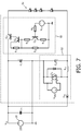
- Figure 7 shows a more specific circuit topology for the circuit of Figure 6 , with the output of the mini boost converter connected to the input supply Vin.
- linear driver 50 It also shows an example of linear driver 50.
- the linear driver comprises a current regulating element in the form of an emitter follower power transistor Q3 between the input and the load.
- the transistor has a controllable resistive characteristic. The resistance is controlled by an input voltage Vin1 which is supplied to the base of a transistor Q1 through a base resistor R5.
- the voltage Vin1 controls the linear driver.
- the voltage Vin1 controls the base current of a transistor Q2, which in turn controls the collector current of transistor Q2 which is the base current of the power transistor Q3.
- the base current of power transistor Q3 changes the current flowing through the linear driver to the load.
- the LED arrangement for example comprises an LED string of rating 200V, 100mA.
- the overall circuit is thus a 20W LED driver, and is based on a on 220V DC grid.
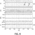
- Figure 8 shows simulation results for the fixed DC input voltage of 220V during a full brightness mode (100mA).
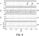
- Figure 9 shows simulation results for the fixed DC input voltage of 220V during a 1/3rd brightness mode (33mA).
- plot (a) shows the output of the mini boost converter as line 80 and the voltage drop across the linear driver as line 82.
- Plot (b) shows the inductor current of the mini boost converter.
- Plot (c) shows the LED current and plot (d) shows the LED voltage.
- the voltage drop across the linear driver is approximately 4V ( ⁇ 2% of 220V DC).
- the LED string voltage at that current is 200V.
- the difference between the input DC grid voltage and LED string voltage, minus the above voltage drop, is absorbed by mini-boost converter 52 to achieve good efficiency.
- the output voltage of the mini-boost converter is 16V during the full brightness mode and is increased to 25V during the 1/3rd brightness mode to absorb the change in LED string voltage because of dimming since in 1/3 brightness the LED string voltage is lowered to 191V.
- the efficiency performance can be calculated.
- Figure 11 shows a method in accordance with an example of the invention.
- the method comprises receiving an input voltage in step 110, providing a current for the load from the input voltage via a driver unit in step 112 and providing a compensating voltage in step 114 thereby to adjust the voltage across the driver unit in dependence on the input voltage and operating conditions of the load.
- the invention has been described above in connection with the driving of LEDs. More generally, the invention is of particular interest for drivers which deliver a controlled current to a load.
- the invention can be used for driving a load with a desired voltage, which enables a step down in voltage from an initial supply to be implemented in an efficient way, and which can enable energy harvesting.
- linear regulator Only one example of linear regulator has been shown. However, other types of linear regulator may be employed.
- the system makes use of a controller.
- Components that may be employed for the controller include, but are not limited to, conventional microprocessors, application specific integrated circuits (ASICs), and field-programmable gate arrays (FPGAs).
- a processor or controller may be associated with one or more storage media such as volatile and non-volatile computer memory such as RAM, PROM, EPROM, and EEPROM.
- the storage media may be encoded with one or more programs that, when executed on one or more processors and/or controllers, perform at the required functions.
- Various storage media may be fixed within a processor or controller or may be transportable, such that the one or more programs stored thereon can be loaded into a processor or controller.
Claims (6)
- Circuit d'attaque pour délivrer un courant à un agencement de LED (51), comprenant :une entrée pour recevoir une tension d'entrée (Vin), comprenant des première et seconde bornes (10a, 10b) ;une unité d'attaque (50) pour fournir un courant régulé pour l'agencement de LED (51) à partir de la tension d'entrée (Vin), dans lequel l'unité d'attaque (50) comprend un dispositif d'attaque linéaire qui comprend un élément de régulation de courant (Q3) pouvant être connecté en série entre l'entrée et l'agencement de LED (51), ledit élément de régulation de courant (Q3) présentant une caractéristique résistive commandable ;caractérisé en ce que le circuit d'attaque comprend en outre :une première unité (56) pour fournir une indication d'une tension de fonctionnement souhaitée (Vdesired) de l'agencement de LED (51) sur la base de conditions de fonctionnement de l'agencement de LED (51) ;une seconde unité (58) configurée pour obtenir la tension d'entrée (Vin) ;un dispositif de commande (54) configuré pour recevoir l'indication de la tension de fonctionnement souhaitée (Vdesired) en provenance de la première unité (56) et de la tension d'entrée (Vin) en provenance de la seconde unité (58), dans lequel le dispositif de commande (54) est configurée pour commander le dispositif d'attaque linéaire (50) de manière à fournir le courant régulé à l'agencement de LED (51) ; etune unité de compensation (52) configurée pour être commandée par le dispositif de commande (54) et pouvoir être connectée en série à l'unité d'attaque (50) et à l'entrée, l'unité de compensation (52) étant configurée pour fournir une tension de compensation, commandant ainsi une chute de tension à travers l'unité d'attaque (50) en fonction de la tension d'entrée et des conditions de fonctionnement de l'agencement de LED (51) ; etdans lequel l'unité de compensation (52) comprend un convertisseur de puissance à mode de commutation (S1, L1, C2, D4), avec un second condensateur (C2) en tant que source d'énergie du convertisseur de puissance à mode de commutation (S1, L1, C2, D4), dans lequel l'élément de régulation de courant (Q3), l'agencement de LED (51) et le second condensateur (C2) peuvent être connectés en série entre les première et seconde bornes (10a, 10b),dans lequel le second condensateur (C2) est adapté pour être chargé par le courant régulé sorti de l'unité d'attaque (50), dans lequel le dispositif de commande (54) est configuré pour faire varier un cycle de service du convertisseur de puissance à mode de commutation (S1, L1, C2, D4) afin de faire varier une chute de tension à travers le second condensateur (C2), de manière à régler la chute de tension à travers le second condensateur (C2) en tant que tension de compensation, qui dicte la tension à travers l'unité d'attaque (50).
- Circuit d'attaque selon la revendication 1, dans lequel le circuit comprend un premier condensateur (C1) entre les première et seconde bornes.
- Circuit d'attaque selon la revendication 1, dans lequel le convertisseur de puissance à mode de commutation comprend un convertisseur élévateur CC-CC inductif, dans lequel le convertisseur élévateur CC-CC inductif comprend le second condensateur (C2), un commutateur de puissance (S1) et un inducteur (L1) et dans lequel le convertisseur élévateur CC-CC présente une sortie qui est adaptée pour se connecter soit à une alimentation à tension externe soit à l'entrée, par le biais d'une diode de sortie (D4).
- Circuit d'attaque selon une quelconque revendication précédente, dans lequel les conditions de fonctionnement de l'agencement de LED (51) comprend un ou plusieurs quelconques parmi les suivants :le courant de fonctionnement ;le vieillissement de l'agencement de LED (51) ; etla température de fonctionnement de la charge d'agencement de LED (51).
- Circuit d'attaque selon la revendication 4, dans lequel :
le dispositif de commande (54) est en outre adapté pour configurer la chute de tension à travers l'unité d'attaque (50) pour avoir une valeur maximale, pour une plage de conditions de fonctionnement autorisées, qui est au maximum k fois une tension de compensation maximale pour la plage de conditions de fonctionnement autorisées, dans lequel k=0,5, plus préférablement k=0,3, encore plus préférablement k=0,2 ; et/ou dans lequel la tension de compensation maximale est inférieure à 0,2 fois une tension d'entrée maximale, dans lequel la tension d'entrée est une tension d'entrée CC. - Circuit d'éclairage, comprenant :un circuit d'attaque selon une quelconque revendication précédente ; etun agencement de LED (51) agencée pour être entraînée par le circuit d'attaque.
Applications Claiming Priority (3)
| Application Number | Priority Date | Filing Date | Title |
|---|---|---|---|
| IN5684CH2014 | 2014-11-12 | ||
| EP15161251 | 2015-03-27 | ||
| PCT/EP2015/076071 WO2016075079A1 (fr) | 2014-11-12 | 2015-11-09 | Circuit d'attaque et procédé |
Publications (2)
| Publication Number | Publication Date |
|---|---|
| EP3219173A1 EP3219173A1 (fr) | 2017-09-20 |
| EP3219173B1 true EP3219173B1 (fr) | 2021-02-24 |
Family
ID=54478029
Family Applications (1)
| Application Number | Title | Priority Date | Filing Date |
|---|---|---|---|
| EP15791294.0A Active EP3219173B1 (fr) | 2014-11-12 | 2015-11-09 | Circuit de commande |
Country Status (6)
| Country | Link |
|---|---|
| US (1) | US10397998B2 (fr) |
| EP (1) | EP3219173B1 (fr) |
| JP (1) | JP6704911B2 (fr) |
| CN (1) | CN107006091B (fr) |
| RU (1) | RU2697830C2 (fr) |
| WO (1) | WO2016075079A1 (fr) |
Families Citing this family (4)
| Publication number | Priority date | Publication date | Assignee | Title |
|---|---|---|---|---|
| DE102009014061A1 (de) * | 2009-03-20 | 2010-09-23 | Zumtobel Lighting Gmbh | Verfahren und System zum effizienten Betreiben einer dimmbaren Leuchte |
| DE102016001689A1 (de) * | 2015-08-07 | 2017-02-09 | DEHN + SÖHNE GmbH + Co. KG. | Schaltungsanordnung zum Schutz einer aus einem Versorgungsnetz zu betreibenden Einheit gegen Überspannungen |
| DE102019100058A1 (de) * | 2019-01-03 | 2020-07-09 | Tridonic Gmbh & Co Kg | Beleuchtungssystem mit Energiespar-Modus und Verfahren zur Optimierung der Gesamteffizienz des Beleuchtungssystems |
| WO2022246805A1 (fr) * | 2021-05-28 | 2022-12-01 | Tridonic Gmbh & Co Kg | Convertisseur à diodes électroluminescentes et dispositif à del |
Family Cites Families (28)
| Publication number | Priority date | Publication date | Assignee | Title |
|---|---|---|---|---|
| US5661645A (en) * | 1996-06-27 | 1997-08-26 | Hochstein; Peter A. | Power supply for light emitting diode array |
| TWI223575B (en) | 2001-10-12 | 2004-11-01 | Koninkl Philips Electronics Nv | Method and apparatus for driving a gas discharge lamp |
| US8441210B2 (en) * | 2006-01-20 | 2013-05-14 | Point Somee Limited Liability Company | Adaptive current regulation for solid state lighting |
| US7902769B2 (en) * | 2006-01-20 | 2011-03-08 | Exclara, Inc. | Current regulator for modulating brightness levels of solid state lighting |
| JP5409399B2 (ja) * | 2007-03-15 | 2014-02-05 | コーニンクレッカ フィリップス エヌ ヴェ | Led、oled又はレーザダイオードのような負荷のための駆動回路 |
| JP2010527223A (ja) * | 2007-05-07 | 2010-08-05 | コーニンクレッカ フィリップス エレクトロニクス エヌ ヴィ | 高い力率のledベースの照明装置及び方法 |
| US7952294B2 (en) | 2008-04-06 | 2011-05-31 | Exclara, Inc. | Apparatus, system and method for cascaded power conversion |
| CN101686587B (zh) * | 2008-09-25 | 2015-01-28 | 皇家飞利浦电子股份有限公司 | 用于向led阵列提供可变功率的驱动器 |
| US8466628B2 (en) * | 2009-10-07 | 2013-06-18 | Lutron Electronics Co., Inc. | Closed-loop load control circuit having a wide output range |
| JP5564239B2 (ja) * | 2009-12-14 | 2014-07-30 | ミネベア株式会社 | Led駆動回路 |
| US8400131B2 (en) | 2010-03-09 | 2013-03-19 | Analog Devices, Inc. | Voltage converter and LED driver circuits with progressive boost, skip, and linear mode operation |
| US8531131B2 (en) * | 2010-09-22 | 2013-09-10 | Osram Sylvania Inc. | Auto-sensing switching regulator to drive a light source through a current regulator |
| KR20130129957A (ko) | 2010-10-24 | 2013-11-29 | 마이크로세미 코포레이션 | Led 구동부를 위한 동기 조절부 |
| US8710752B2 (en) | 2011-03-03 | 2014-04-29 | Dialog Semiconductor Inc. | Adaptive switch mode LED system |
| US8773085B2 (en) * | 2011-03-22 | 2014-07-08 | Ledillion Technologies Inc. | Apparatus and method for efficient DC-to-DC conversion through wide voltage swings |
| JP5792504B2 (ja) * | 2011-04-28 | 2015-10-14 | ローム株式会社 | 電源装置およびその制御回路、電子機器 |
| US9370064B2 (en) | 2011-10-06 | 2016-06-14 | National Semiconductor Corporation | LED driver having non-linear compensation |
| US8704449B2 (en) * | 2012-05-09 | 2014-04-22 | Shenzhen China Star Optoelectronics Technology Co., Ltd. | LED backlight driving circuit, liquid crystal display device and driving circuit |
| US8994639B2 (en) * | 2012-05-16 | 2015-03-31 | Shenzhen China Star Optoelectronics Technology Co., Ltd. | LED backlight driving circuit, backlight module, and LCD device |
| WO2014080337A2 (fr) | 2012-11-26 | 2014-05-30 | Koninklijke Philips N.V. | Commande basée sur niveau de signal de systèmes de charge de réseau électrique |
| GB2509099A (en) | 2012-12-20 | 2014-06-25 | Accuric Ltd | LED driver circuit |
| US9866117B2 (en) * | 2013-03-11 | 2018-01-09 | Cree, Inc. | Power supply with adaptive-controlled output voltage |
| EP2779791A1 (fr) * | 2013-03-12 | 2014-09-17 | Power Research Electronics B.v. | Circuit de commande à DEL |
| US9743472B2 (en) | 2013-03-15 | 2017-08-22 | City University Of Hong Kong | Electrical load driving apparatus |
| WO2014186776A1 (fr) | 2013-05-17 | 2014-11-20 | Cirrus Logic, Inc. | Circuit à pompe de charge pour l'alimentation électrique par un transistor à jonctions bipolaires (bjt) |
| CN103269548B (zh) * | 2013-05-29 | 2015-07-08 | 成都芯源系统有限公司 | Led驱动电路系统,控制器及控制方法 |
| CN104869686A (zh) * | 2014-02-26 | 2015-08-26 | 欧司朗有限公司 | 驱动电路和包括该驱动电路的照明装置 |
| US9618162B2 (en) * | 2014-04-25 | 2017-04-11 | Cree, Inc. | LED lamp |
-
2015
- 2015-11-09 EP EP15791294.0A patent/EP3219173B1/fr active Active
- 2015-11-09 CN CN201580061460.8A patent/CN107006091B/zh active Active
- 2015-11-09 WO PCT/EP2015/076071 patent/WO2016075079A1/fr active Application Filing
- 2015-11-09 RU RU2017120304A patent/RU2697830C2/ru active
- 2015-11-09 US US15/525,547 patent/US10397998B2/en active Active
- 2015-11-09 JP JP2017525406A patent/JP6704911B2/ja active Active
Non-Patent Citations (1)
| Title |
|---|
| None * |
Also Published As
| Publication number | Publication date |
|---|---|
| CN107006091B (zh) | 2019-06-14 |
| CN107006091A (zh) | 2017-08-01 |
| US20170325306A1 (en) | 2017-11-09 |
| RU2017120304A (ru) | 2018-12-13 |
| US10397998B2 (en) | 2019-08-27 |
| WO2016075079A1 (fr) | 2016-05-19 |
| RU2017120304A3 (fr) | 2019-06-21 |
| JP6704911B2 (ja) | 2020-06-03 |
| RU2697830C2 (ru) | 2019-08-21 |
| EP3219173A1 (fr) | 2017-09-20 |
| JP2017534155A (ja) | 2017-11-16 |
Similar Documents
| Publication | Publication Date | Title |
|---|---|---|
| US10517154B2 (en) | Load control device having a wide output range | |
| US9791110B2 (en) | High efficiency driver circuit with fast response | |
| US10645776B2 (en) | Turn-on procedure for a load control device | |
| US8253352B2 (en) | Circuits and methods for powering light sources | |
| US9374860B2 (en) | Lighting device | |
| EP2315497A1 (fr) | Circuit de commande avec contrôle de la tension de réserve et correction du facteur de puissance | |
| EP3113578B1 (fr) | Circuit de filtre | |
| US10136487B2 (en) | Power optimization for linear regulator | |
| EP3219173B1 (fr) | Circuit de commande | |
| JP6320455B2 (ja) | Led点灯装置 | |
| US10334681B2 (en) | Device for driving light emitting element | |
| CN107079555B (zh) | 线性后调节器 | |
| US10271391B2 (en) | Light emitting diode driver | |
| US11166356B2 (en) | Constant current driver charging energy storage unit | |
| WO2020122249A1 (fr) | Dispositif d'émission de lumière à del | |
| JP6532002B2 (ja) | 照明装置及び電源ユニット | |
| KR101988660B1 (ko) | Led 모듈 구동 회로 | |
| CN112369124A (zh) | 光源驱动装置及其方法 | |
| EP2958401A1 (fr) | Circuit de commande de DEL et procédé associé à une commande de DEL |
Legal Events
| Date | Code | Title | Description |
|---|---|---|---|
| STAA | Information on the status of an ep patent application or granted ep patent |
Free format text: STATUS: THE INTERNATIONAL PUBLICATION HAS BEEN MADE |
|
| PUAI | Public reference made under article 153(3) epc to a published international application that has entered the european phase |
Free format text: ORIGINAL CODE: 0009012 |
|
| STAA | Information on the status of an ep patent application or granted ep patent |
Free format text: STATUS: REQUEST FOR EXAMINATION WAS MADE |
|
| 17P | Request for examination filed |
Effective date: 20170612 |
|
| AK | Designated contracting states |
Kind code of ref document: A1 Designated state(s): AL AT BE BG CH CY CZ DE DK EE ES FI FR GB GR HR HU IE IS IT LI LT LU LV MC MK MT NL NO PL PT RO RS SE SI SK SM TR |
|
| AX | Request for extension of the european patent |
Extension state: BA ME |
|
| DAV | Request for validation of the european patent (deleted) | ||
| DAX | Request for extension of the european patent (deleted) | ||
| RAP1 | Party data changed (applicant data changed or rights of an application transferred) |
Owner name: PHILIPS LIGHTING HOLDING B.V. |
|
| RAP1 | Party data changed (applicant data changed or rights of an application transferred) |
Owner name: SIGNIFY HOLDING B.V. |
|
| STAA | Information on the status of an ep patent application or granted ep patent |
Free format text: STATUS: EXAMINATION IS IN PROGRESS |
|
| 17Q | First examination report despatched |
Effective date: 20190719 |
|
| REG | Reference to a national code |
Ref country code: DE Ref legal event code: R079 Ref document number: 602015066059 Country of ref document: DE Free format text: PREVIOUS MAIN CLASS: H05B0033080000 Ipc: H05B0045370000 |
|
| GRAP | Despatch of communication of intention to grant a patent |
Free format text: ORIGINAL CODE: EPIDOSNIGR1 |
|
| STAA | Information on the status of an ep patent application or granted ep patent |
Free format text: STATUS: GRANT OF PATENT IS INTENDED |
|
| RIC1 | Information provided on ipc code assigned before grant |
Ipc: H05B 45/37 20200101AFI20200909BHEP |
|
| INTG | Intention to grant announced |
Effective date: 20201002 |
|
| GRAS | Grant fee paid |
Free format text: ORIGINAL CODE: EPIDOSNIGR3 |
|
| GRAA | (expected) grant |
Free format text: ORIGINAL CODE: 0009210 |
|
| STAA | Information on the status of an ep patent application or granted ep patent |
Free format text: STATUS: THE PATENT HAS BEEN GRANTED |
|
| AK | Designated contracting states |
Kind code of ref document: B1 Designated state(s): AL AT BE BG CH CY CZ DE DK EE ES FI FR GB GR HR HU IE IS IT LI LT LU LV MC MK MT NL NO PL PT RO RS SE SI SK SM TR |
|
| REG | Reference to a national code |
Ref country code: GB Ref legal event code: FG4D |
|
| REG | Reference to a national code |
Ref country code: CH Ref legal event code: EP |
|
| REG | Reference to a national code |
Ref country code: AT Ref legal event code: REF Ref document number: 1366120 Country of ref document: AT Kind code of ref document: T Effective date: 20210315 |
|
| REG | Reference to a national code |
Ref country code: IE Ref legal event code: FG4D |
|
| REG | Reference to a national code |
Ref country code: DE Ref legal event code: R096 Ref document number: 602015066059 Country of ref document: DE |
|
| REG | Reference to a national code |
Ref country code: LT Ref legal event code: MG9D |
|
| REG | Reference to a national code |
Ref country code: NL Ref legal event code: MP Effective date: 20210224 |
|
| PG25 | Lapsed in a contracting state [announced via postgrant information from national office to epo] |
Ref country code: HR Free format text: LAPSE BECAUSE OF FAILURE TO SUBMIT A TRANSLATION OF THE DESCRIPTION OR TO PAY THE FEE WITHIN THE PRESCRIBED TIME-LIMIT Effective date: 20210224 Ref country code: FI Free format text: LAPSE BECAUSE OF FAILURE TO SUBMIT A TRANSLATION OF THE DESCRIPTION OR TO PAY THE FEE WITHIN THE PRESCRIBED TIME-LIMIT Effective date: 20210224 Ref country code: GR Free format text: LAPSE BECAUSE OF FAILURE TO SUBMIT A TRANSLATION OF THE DESCRIPTION OR TO PAY THE FEE WITHIN THE PRESCRIBED TIME-LIMIT Effective date: 20210525 Ref country code: BG Free format text: LAPSE BECAUSE OF FAILURE TO SUBMIT A TRANSLATION OF THE DESCRIPTION OR TO PAY THE FEE WITHIN THE PRESCRIBED TIME-LIMIT Effective date: 20210524 Ref country code: NO Free format text: LAPSE BECAUSE OF FAILURE TO SUBMIT A TRANSLATION OF THE DESCRIPTION OR TO PAY THE FEE WITHIN THE PRESCRIBED TIME-LIMIT Effective date: 20210524 Ref country code: PT Free format text: LAPSE BECAUSE OF FAILURE TO SUBMIT A TRANSLATION OF THE DESCRIPTION OR TO PAY THE FEE WITHIN THE PRESCRIBED TIME-LIMIT Effective date: 20210624 Ref country code: LT Free format text: LAPSE BECAUSE OF FAILURE TO SUBMIT A TRANSLATION OF THE DESCRIPTION OR TO PAY THE FEE WITHIN THE PRESCRIBED TIME-LIMIT Effective date: 20210224 |
|
| REG | Reference to a national code |
Ref country code: AT Ref legal event code: MK05 Ref document number: 1366120 Country of ref document: AT Kind code of ref document: T Effective date: 20210224 |
|
| PG25 | Lapsed in a contracting state [announced via postgrant information from national office to epo] |
Ref country code: NL Free format text: LAPSE BECAUSE OF FAILURE TO SUBMIT A TRANSLATION OF THE DESCRIPTION OR TO PAY THE FEE WITHIN THE PRESCRIBED TIME-LIMIT Effective date: 20210224 Ref country code: RS Free format text: LAPSE BECAUSE OF FAILURE TO SUBMIT A TRANSLATION OF THE DESCRIPTION OR TO PAY THE FEE WITHIN THE PRESCRIBED TIME-LIMIT Effective date: 20210224 Ref country code: PL Free format text: LAPSE BECAUSE OF FAILURE TO SUBMIT A TRANSLATION OF THE DESCRIPTION OR TO PAY THE FEE WITHIN THE PRESCRIBED TIME-LIMIT Effective date: 20210224 Ref country code: LV Free format text: LAPSE BECAUSE OF FAILURE TO SUBMIT A TRANSLATION OF THE DESCRIPTION OR TO PAY THE FEE WITHIN THE PRESCRIBED TIME-LIMIT Effective date: 20210224 Ref country code: SE Free format text: LAPSE BECAUSE OF FAILURE TO SUBMIT A TRANSLATION OF THE DESCRIPTION OR TO PAY THE FEE WITHIN THE PRESCRIBED TIME-LIMIT Effective date: 20210224 |
|
| PG25 | Lapsed in a contracting state [announced via postgrant information from national office to epo] |
Ref country code: IS Free format text: LAPSE BECAUSE OF FAILURE TO SUBMIT A TRANSLATION OF THE DESCRIPTION OR TO PAY THE FEE WITHIN THE PRESCRIBED TIME-LIMIT Effective date: 20210624 |
|
| PG25 | Lapsed in a contracting state [announced via postgrant information from national office to epo] |
Ref country code: EE Free format text: LAPSE BECAUSE OF FAILURE TO SUBMIT A TRANSLATION OF THE DESCRIPTION OR TO PAY THE FEE WITHIN THE PRESCRIBED TIME-LIMIT Effective date: 20210224 Ref country code: CZ Free format text: LAPSE BECAUSE OF FAILURE TO SUBMIT A TRANSLATION OF THE DESCRIPTION OR TO PAY THE FEE WITHIN THE PRESCRIBED TIME-LIMIT Effective date: 20210224 Ref country code: SM Free format text: LAPSE BECAUSE OF FAILURE TO SUBMIT A TRANSLATION OF THE DESCRIPTION OR TO PAY THE FEE WITHIN THE PRESCRIBED TIME-LIMIT Effective date: 20210224 Ref country code: AT Free format text: LAPSE BECAUSE OF FAILURE TO SUBMIT A TRANSLATION OF THE DESCRIPTION OR TO PAY THE FEE WITHIN THE PRESCRIBED TIME-LIMIT Effective date: 20210224 |
|
| REG | Reference to a national code |
Ref country code: DE Ref legal event code: R097 Ref document number: 602015066059 Country of ref document: DE |
|
| PG25 | Lapsed in a contracting state [announced via postgrant information from national office to epo] |
Ref country code: SK Free format text: LAPSE BECAUSE OF FAILURE TO SUBMIT A TRANSLATION OF THE DESCRIPTION OR TO PAY THE FEE WITHIN THE PRESCRIBED TIME-LIMIT Effective date: 20210224 Ref country code: RO Free format text: LAPSE BECAUSE OF FAILURE TO SUBMIT A TRANSLATION OF THE DESCRIPTION OR TO PAY THE FEE WITHIN THE PRESCRIBED TIME-LIMIT Effective date: 20210224 Ref country code: DK Free format text: LAPSE BECAUSE OF FAILURE TO SUBMIT A TRANSLATION OF THE DESCRIPTION OR TO PAY THE FEE WITHIN THE PRESCRIBED TIME-LIMIT Effective date: 20210224 |
|
| PLBE | No opposition filed within time limit |
Free format text: ORIGINAL CODE: 0009261 |
|
| STAA | Information on the status of an ep patent application or granted ep patent |
Free format text: STATUS: NO OPPOSITION FILED WITHIN TIME LIMIT |
|
| PG25 | Lapsed in a contracting state [announced via postgrant information from national office to epo] |
Ref country code: ES Free format text: LAPSE BECAUSE OF FAILURE TO SUBMIT A TRANSLATION OF THE DESCRIPTION OR TO PAY THE FEE WITHIN THE PRESCRIBED TIME-LIMIT Effective date: 20210224 Ref country code: AL Free format text: LAPSE BECAUSE OF FAILURE TO SUBMIT A TRANSLATION OF THE DESCRIPTION OR TO PAY THE FEE WITHIN THE PRESCRIBED TIME-LIMIT Effective date: 20210224 |
|
| 26N | No opposition filed |
Effective date: 20211125 |
|
| PG25 | Lapsed in a contracting state [announced via postgrant information from national office to epo] |
Ref country code: SI Free format text: LAPSE BECAUSE OF FAILURE TO SUBMIT A TRANSLATION OF THE DESCRIPTION OR TO PAY THE FEE WITHIN THE PRESCRIBED TIME-LIMIT Effective date: 20210224 |
|
| PG25 | Lapsed in a contracting state [announced via postgrant information from national office to epo] |
Ref country code: IT Free format text: LAPSE BECAUSE OF FAILURE TO SUBMIT A TRANSLATION OF THE DESCRIPTION OR TO PAY THE FEE WITHIN THE PRESCRIBED TIME-LIMIT Effective date: 20210224 |
|
| PG25 | Lapsed in a contracting state [announced via postgrant information from national office to epo] |
Ref country code: IS Free format text: LAPSE BECAUSE OF FAILURE TO SUBMIT A TRANSLATION OF THE DESCRIPTION OR TO PAY THE FEE WITHIN THE PRESCRIBED TIME-LIMIT Effective date: 20210624 |
|
| PG25 | Lapsed in a contracting state [announced via postgrant information from national office to epo] |
Ref country code: MC Free format text: LAPSE BECAUSE OF FAILURE TO SUBMIT A TRANSLATION OF THE DESCRIPTION OR TO PAY THE FEE WITHIN THE PRESCRIBED TIME-LIMIT Effective date: 20210224 |
|
| REG | Reference to a national code |
Ref country code: CH Ref legal event code: PL |
|
| PG25 | Lapsed in a contracting state [announced via postgrant information from national office to epo] |
Ref country code: LU Free format text: LAPSE BECAUSE OF NON-PAYMENT OF DUE FEES Effective date: 20211109 Ref country code: BE Free format text: LAPSE BECAUSE OF NON-PAYMENT OF DUE FEES Effective date: 20211130 |
|
| REG | Reference to a national code |
Ref country code: BE Ref legal event code: MM Effective date: 20211130 |
|
| PG25 | Lapsed in a contracting state [announced via postgrant information from national office to epo] |
Ref country code: LI Free format text: LAPSE BECAUSE OF NON-PAYMENT OF DUE FEES Effective date: 20211130 Ref country code: CH Free format text: LAPSE BECAUSE OF NON-PAYMENT OF DUE FEES Effective date: 20211130 |
|
| PG25 | Lapsed in a contracting state [announced via postgrant information from national office to epo] |
Ref country code: IE Free format text: LAPSE BECAUSE OF NON-PAYMENT OF DUE FEES Effective date: 20211109 |
|
| PG25 | Lapsed in a contracting state [announced via postgrant information from national office to epo] |
Ref country code: HU Free format text: LAPSE BECAUSE OF FAILURE TO SUBMIT A TRANSLATION OF THE DESCRIPTION OR TO PAY THE FEE WITHIN THE PRESCRIBED TIME-LIMIT; INVALID AB INITIO Effective date: 20151109 |
|
| P01 | Opt-out of the competence of the unified patent court (upc) registered |
Effective date: 20230425 |
|
| PG25 | Lapsed in a contracting state [announced via postgrant information from national office to epo] |
Ref country code: CY Free format text: LAPSE BECAUSE OF FAILURE TO SUBMIT A TRANSLATION OF THE DESCRIPTION OR TO PAY THE FEE WITHIN THE PRESCRIBED TIME-LIMIT Effective date: 20210224 |
|
| PGFP | Annual fee paid to national office [announced via postgrant information from national office to epo] |
Ref country code: GB Payment date: 20231121 Year of fee payment: 9 |
|
| PGFP | Annual fee paid to national office [announced via postgrant information from national office to epo] |
Ref country code: FR Payment date: 20231123 Year of fee payment: 9 |
|
| PG25 | Lapsed in a contracting state [announced via postgrant information from national office to epo] |
Ref country code: MK Free format text: LAPSE BECAUSE OF FAILURE TO SUBMIT A TRANSLATION OF THE DESCRIPTION OR TO PAY THE FEE WITHIN THE PRESCRIBED TIME-LIMIT Effective date: 20210224 |
|
| PGFP | Annual fee paid to national office [announced via postgrant information from national office to epo] |
Ref country code: DE Payment date: 20240129 Year of fee payment: 9 |