EP3213345B1 - High density fan out package structure - Google Patents
High density fan out package structure Download PDFInfo
- Publication number
- EP3213345B1 EP3213345B1 EP15767632.1A EP15767632A EP3213345B1 EP 3213345 B1 EP3213345 B1 EP 3213345B1 EP 15767632 A EP15767632 A EP 15767632A EP 3213345 B1 EP3213345 B1 EP 3213345B1
- Authority
- EP
- European Patent Office
- Prior art keywords
- layer
- conductive
- package structure
- conductive interconnect
- fan out
- Prior art date
- Legal status (The legal status is an assumption and is not a legal conclusion. Google has not performed a legal analysis and makes no representation as to the accuracy of the status listed.)
- Active
Links
- 238000000034 method Methods 0.000 claims description 62
- 239000000758 substrate Substances 0.000 claims description 61
- 230000004888 barrier function Effects 0.000 claims description 44
- 239000004020 conductor Substances 0.000 claims description 17
- 238000000151 deposition Methods 0.000 claims description 12
- 238000004891 communication Methods 0.000 claims description 11
- 229910052715 tantalum Inorganic materials 0.000 claims description 7
- GUVRBAGPIYLISA-UHFFFAOYSA-N tantalum atom Chemical compound [Ta] GUVRBAGPIYLISA-UHFFFAOYSA-N 0.000 claims description 7
- 235000012431 wafers Nutrition 0.000 description 49
- 239000000463 material Substances 0.000 description 46
- 230000008569 process Effects 0.000 description 41
- 239000004065 semiconductor Substances 0.000 description 35
- 238000004519 manufacturing process Methods 0.000 description 23
- 238000003860 storage Methods 0.000 description 23
- 230000015572 biosynthetic process Effects 0.000 description 13
- 238000013461 design Methods 0.000 description 13
- 230000006870 function Effects 0.000 description 10
- 230000015654 memory Effects 0.000 description 10
- 230000008878 coupling Effects 0.000 description 9
- 238000010168 coupling process Methods 0.000 description 9
- 238000005859 coupling reaction Methods 0.000 description 9
- 239000013078 crystal Substances 0.000 description 9
- 229910000679 solder Inorganic materials 0.000 description 9
- 238000010586 diagram Methods 0.000 description 8
- 238000004806 packaging method and process Methods 0.000 description 7
- 229920000642 polymer Polymers 0.000 description 7
- RYGMFSIKBFXOCR-UHFFFAOYSA-N Copper Chemical compound [Cu] RYGMFSIKBFXOCR-UHFFFAOYSA-N 0.000 description 6
- 239000002800 charge carrier Substances 0.000 description 6
- 229910052802 copper Inorganic materials 0.000 description 6
- 239000010949 copper Substances 0.000 description 6
- 239000003989 dielectric material Substances 0.000 description 5
- 238000005516 engineering process Methods 0.000 description 5
- 230000002950 deficient Effects 0.000 description 4
- 239000002019 doping agent Substances 0.000 description 4
- 229910052751 metal Inorganic materials 0.000 description 4
- 239000002184 metal Substances 0.000 description 4
- 150000004767 nitrides Chemical class 0.000 description 4
- 230000003287 optical effect Effects 0.000 description 4
- XUIMIQQOPSSXEZ-UHFFFAOYSA-N Silicon Chemical compound [Si] XUIMIQQOPSSXEZ-UHFFFAOYSA-N 0.000 description 3
- 230000007547 defect Effects 0.000 description 3
- 230000009977 dual effect Effects 0.000 description 3
- 239000012212 insulator Substances 0.000 description 3
- 239000000203 mixture Substances 0.000 description 3
- 229910052710 silicon Inorganic materials 0.000 description 3
- 239000010703 silicon Substances 0.000 description 3
- VYPSYNLAJGMNEJ-UHFFFAOYSA-N silicon dioxide Inorganic materials O=[Si]=O VYPSYNLAJGMNEJ-UHFFFAOYSA-N 0.000 description 3
- 229910000530 Gallium indium arsenide Inorganic materials 0.000 description 2
- JMASRVWKEDWRBT-UHFFFAOYSA-N Gallium nitride Chemical compound [Ga]#N JMASRVWKEDWRBT-UHFFFAOYSA-N 0.000 description 2
- 229910052581 Si3N4 Inorganic materials 0.000 description 2
- KXNLCSXBJCPWGL-UHFFFAOYSA-N [Ga].[As].[In] Chemical compound [Ga].[As].[In] KXNLCSXBJCPWGL-UHFFFAOYSA-N 0.000 description 2
- 239000000654 additive Substances 0.000 description 2
- 238000004590 computer program Methods 0.000 description 2
- 238000009792 diffusion process Methods 0.000 description 2
- 238000009713 electroplating Methods 0.000 description 2
- 238000005530 etching Methods 0.000 description 2
- 239000000835 fiber Substances 0.000 description 2
- 239000011521 glass Substances 0.000 description 2
- 238000000227 grinding Methods 0.000 description 2
- 238000002955 isolation Methods 0.000 description 2
- 238000002161 passivation Methods 0.000 description 2
- 238000005498 polishing Methods 0.000 description 2
- 235000012239 silicon dioxide Nutrition 0.000 description 2
- HQVNEWCFYHHQES-UHFFFAOYSA-N silicon nitride Chemical compound N12[Si]34N5[Si]62N3[Si]51N64 HQVNEWCFYHHQES-UHFFFAOYSA-N 0.000 description 2
- 239000000126 substance Substances 0.000 description 2
- 238000012360 testing method Methods 0.000 description 2
- JBRZTFJDHDCESZ-UHFFFAOYSA-N AsGa Chemical compound [As]#[Ga] JBRZTFJDHDCESZ-UHFFFAOYSA-N 0.000 description 1
- ZOXJGFHDIHLPTG-UHFFFAOYSA-N Boron Chemical compound [B] ZOXJGFHDIHLPTG-UHFFFAOYSA-N 0.000 description 1
- 238000002231 Czochralski process Methods 0.000 description 1
- 229910002601 GaN Inorganic materials 0.000 description 1
- OAICVXFJPJFONN-UHFFFAOYSA-N Phosphorus Chemical compound [P] OAICVXFJPJFONN-UHFFFAOYSA-N 0.000 description 1
- 230000000996 additive effect Effects 0.000 description 1
- 229910045601 alloy Inorganic materials 0.000 description 1
- 239000000956 alloy Substances 0.000 description 1
- 230000004075 alteration Effects 0.000 description 1
- 229910052782 aluminium Inorganic materials 0.000 description 1
- XAGFODPZIPBFFR-UHFFFAOYSA-N aluminium Chemical compound [Al] XAGFODPZIPBFFR-UHFFFAOYSA-N 0.000 description 1
- 238000013459 approach Methods 0.000 description 1
- 230000005540 biological transmission Effects 0.000 description 1
- 229910052796 boron Inorganic materials 0.000 description 1
- 239000003990 capacitor Substances 0.000 description 1
- 230000008859 change Effects 0.000 description 1
- 238000005229 chemical vapour deposition Methods 0.000 description 1
- 150000001875 compounds Chemical class 0.000 description 1
- 238000010276 construction Methods 0.000 description 1
- 230000003247 decreasing effect Effects 0.000 description 1
- 230000008021 deposition Effects 0.000 description 1
- 238000000609 electron-beam lithography Methods 0.000 description 1
- 230000005669 field effect Effects 0.000 description 1
- 238000002513 implantation Methods 0.000 description 1
- 229910052738 indium Inorganic materials 0.000 description 1
- APFVFJFRJDLVQX-UHFFFAOYSA-N indium atom Chemical compound [In] APFVFJFRJDLVQX-UHFFFAOYSA-N 0.000 description 1
- 230000003993 interaction Effects 0.000 description 1
- 238000005468 ion implantation Methods 0.000 description 1
- 150000002500 ions Chemical class 0.000 description 1
- 230000007774 longterm Effects 0.000 description 1
- 230000000873 masking effect Effects 0.000 description 1
- 239000007769 metal material Substances 0.000 description 1
- 238000001465 metallisation Methods 0.000 description 1
- 239000012768 molten material Substances 0.000 description 1
- 230000008520 organization Effects 0.000 description 1
- 238000000059 patterning Methods 0.000 description 1
- 229910052698 phosphorus Inorganic materials 0.000 description 1
- 239000011574 phosphorus Substances 0.000 description 1
- 238000000206 photolithography Methods 0.000 description 1
- 229920002120 photoresistant polymer Polymers 0.000 description 1
- 238000001020 plasma etching Methods 0.000 description 1
- 238000002360 preparation method Methods 0.000 description 1
- 238000012545 processing Methods 0.000 description 1
- 239000010453 quartz Substances 0.000 description 1
- 230000005855 radiation Effects 0.000 description 1
- 239000000523 sample Substances 0.000 description 1
- 229910021332 silicide Inorganic materials 0.000 description 1
- FVBUAEGBCNSCDD-UHFFFAOYSA-N silicide(4-) Chemical compound [Si-4] FVBUAEGBCNSCDD-UHFFFAOYSA-N 0.000 description 1
- 239000000377 silicon dioxide Substances 0.000 description 1
- 238000004088 simulation Methods 0.000 description 1
- 125000006850 spacer group Chemical group 0.000 description 1
- 238000006467 substitution reaction Methods 0.000 description 1
- 238000012546 transfer Methods 0.000 description 1
- WFKWXMTUELFFGS-UHFFFAOYSA-N tungsten Chemical compound [W] WFKWXMTUELFFGS-UHFFFAOYSA-N 0.000 description 1
- 229910052721 tungsten Inorganic materials 0.000 description 1
- 239000010937 tungsten Substances 0.000 description 1
- 239000013598 vector Substances 0.000 description 1
- 238000012795 verification Methods 0.000 description 1
- 238000001039 wet etching Methods 0.000 description 1
Images


Classifications
-
- H—ELECTRICITY
- H01—ELECTRIC ELEMENTS
- H01L—SEMICONDUCTOR DEVICES NOT COVERED BY CLASS H10
- H01L23/00—Details of semiconductor or other solid state devices
- H01L23/48—Arrangements for conducting electric current to or from the solid state body in operation, e.g. leads, terminal arrangements ; Selection of materials therefor
- H01L23/488—Arrangements for conducting electric current to or from the solid state body in operation, e.g. leads, terminal arrangements ; Selection of materials therefor consisting of soldered or bonded constructions
- H01L23/498—Leads, i.e. metallisations or lead-frames on insulating substrates, e.g. chip carriers
- H01L23/49811—Additional leads joined to the metallisation on the insulating substrate, e.g. pins, bumps, wires, flat leads
- H01L23/49816—Spherical bumps on the substrate for external connection, e.g. ball grid arrays [BGA]
-
- H—ELECTRICITY
- H01—ELECTRIC ELEMENTS
- H01L—SEMICONDUCTOR DEVICES NOT COVERED BY CLASS H10
- H01L21/00—Processes or apparatus adapted for the manufacture or treatment of semiconductor or solid state devices or of parts thereof
- H01L21/02—Manufacture or treatment of semiconductor devices or of parts thereof
- H01L21/04—Manufacture or treatment of semiconductor devices or of parts thereof the devices having potential barriers, e.g. a PN junction, depletion layer or carrier concentration layer
- H01L21/48—Manufacture or treatment of parts, e.g. containers, prior to assembly of the devices, using processes not provided for in a single one of the groups H01L21/18 - H01L21/326 or H10D48/04 - H10D48/07
- H01L21/4814—Conductive parts
- H01L21/4846—Leads on or in insulating or insulated substrates, e.g. metallisation
- H01L21/4853—Connection or disconnection of other leads to or from a metallisation, e.g. pins, wires, bumps
-
- H—ELECTRICITY
- H01—ELECTRIC ELEMENTS
- H01L—SEMICONDUCTOR DEVICES NOT COVERED BY CLASS H10
- H01L21/00—Processes or apparatus adapted for the manufacture or treatment of semiconductor or solid state devices or of parts thereof
- H01L21/02—Manufacture or treatment of semiconductor devices or of parts thereof
- H01L21/04—Manufacture or treatment of semiconductor devices or of parts thereof the devices having potential barriers, e.g. a PN junction, depletion layer or carrier concentration layer
- H01L21/48—Manufacture or treatment of parts, e.g. containers, prior to assembly of the devices, using processes not provided for in a single one of the groups H01L21/18 - H01L21/326 or H10D48/04 - H10D48/07
- H01L21/4814—Conductive parts
- H01L21/4846—Leads on or in insulating or insulated substrates, e.g. metallisation
- H01L21/486—Via connections through the substrate with or without pins
-
- H—ELECTRICITY
- H01—ELECTRIC ELEMENTS
- H01L—SEMICONDUCTOR DEVICES NOT COVERED BY CLASS H10
- H01L21/00—Processes or apparatus adapted for the manufacture or treatment of semiconductor or solid state devices or of parts thereof
- H01L21/67—Apparatus specially adapted for handling semiconductor or electric solid state devices during manufacture or treatment thereof; Apparatus specially adapted for handling wafers during manufacture or treatment of semiconductor or electric solid state devices or components ; Apparatus not specifically provided for elsewhere
- H01L21/683—Apparatus specially adapted for handling semiconductor or electric solid state devices during manufacture or treatment thereof; Apparatus specially adapted for handling wafers during manufacture or treatment of semiconductor or electric solid state devices or components ; Apparatus not specifically provided for elsewhere for supporting or gripping
- H01L21/6835—Apparatus specially adapted for handling semiconductor or electric solid state devices during manufacture or treatment thereof; Apparatus specially adapted for handling wafers during manufacture or treatment of semiconductor or electric solid state devices or components ; Apparatus not specifically provided for elsewhere for supporting or gripping using temporarily an auxiliary support
-
- H—ELECTRICITY
- H01—ELECTRIC ELEMENTS
- H01L—SEMICONDUCTOR DEVICES NOT COVERED BY CLASS H10
- H01L23/00—Details of semiconductor or other solid state devices
- H01L23/48—Arrangements for conducting electric current to or from the solid state body in operation, e.g. leads, terminal arrangements ; Selection of materials therefor
- H01L23/488—Arrangements for conducting electric current to or from the solid state body in operation, e.g. leads, terminal arrangements ; Selection of materials therefor consisting of soldered or bonded constructions
- H01L23/498—Leads, i.e. metallisations or lead-frames on insulating substrates, e.g. chip carriers
- H01L23/49827—Via connections through the substrates, e.g. pins going through the substrate, coaxial cables
-
- H—ELECTRICITY
- H01—ELECTRIC ELEMENTS
- H01L—SEMICONDUCTOR DEVICES NOT COVERED BY CLASS H10
- H01L23/00—Details of semiconductor or other solid state devices
- H01L23/48—Arrangements for conducting electric current to or from the solid state body in operation, e.g. leads, terminal arrangements ; Selection of materials therefor
- H01L23/488—Arrangements for conducting electric current to or from the solid state body in operation, e.g. leads, terminal arrangements ; Selection of materials therefor consisting of soldered or bonded constructions
- H01L23/498—Leads, i.e. metallisations or lead-frames on insulating substrates, e.g. chip carriers
- H01L23/49838—Geometry or layout
-
- H—ELECTRICITY
- H01—ELECTRIC ELEMENTS
- H01L—SEMICONDUCTOR DEVICES NOT COVERED BY CLASS H10
- H01L23/00—Details of semiconductor or other solid state devices
- H01L23/48—Arrangements for conducting electric current to or from the solid state body in operation, e.g. leads, terminal arrangements ; Selection of materials therefor
- H01L23/488—Arrangements for conducting electric current to or from the solid state body in operation, e.g. leads, terminal arrangements ; Selection of materials therefor consisting of soldered or bonded constructions
- H01L23/498—Leads, i.e. metallisations or lead-frames on insulating substrates, e.g. chip carriers
- H01L23/49866—Leads, i.e. metallisations or lead-frames on insulating substrates, e.g. chip carriers characterised by the materials
-
- H—ELECTRICITY
- H01—ELECTRIC ELEMENTS
- H01L—SEMICONDUCTOR DEVICES NOT COVERED BY CLASS H10
- H01L24/00—Arrangements for connecting or disconnecting semiconductor or solid-state bodies; Methods or apparatus related thereto
- H01L24/01—Means for bonding being attached to, or being formed on, the surface to be connected, e.g. chip-to-package, die-attach, "first-level" interconnects; Manufacturing methods related thereto
- H01L24/02—Bonding areas ; Manufacturing methods related thereto
- H01L24/03—Manufacturing methods
-
- H—ELECTRICITY
- H01—ELECTRIC ELEMENTS
- H01L—SEMICONDUCTOR DEVICES NOT COVERED BY CLASS H10
- H01L24/00—Arrangements for connecting or disconnecting semiconductor or solid-state bodies; Methods or apparatus related thereto
- H01L24/01—Means for bonding being attached to, or being formed on, the surface to be connected, e.g. chip-to-package, die-attach, "first-level" interconnects; Manufacturing methods related thereto
- H01L24/02—Bonding areas ; Manufacturing methods related thereto
- H01L24/07—Structure, shape, material or disposition of the bonding areas after the connecting process
- H01L24/09—Structure, shape, material or disposition of the bonding areas after the connecting process of a plurality of bonding areas
-
- H—ELECTRICITY
- H01—ELECTRIC ELEMENTS
- H01L—SEMICONDUCTOR DEVICES NOT COVERED BY CLASS H10
- H01L24/00—Arrangements for connecting or disconnecting semiconductor or solid-state bodies; Methods or apparatus related thereto
- H01L24/80—Methods for connecting semiconductor or other solid state bodies using means for bonding being attached to, or being formed on, the surface to be connected
- H01L24/81—Methods for connecting semiconductor or other solid state bodies using means for bonding being attached to, or being formed on, the surface to be connected using a bump connector
-
- H—ELECTRICITY
- H01—ELECTRIC ELEMENTS
- H01L—SEMICONDUCTOR DEVICES NOT COVERED BY CLASS H10
- H01L2221/00—Processes or apparatus adapted for the manufacture or treatment of semiconductor or solid state devices or of parts thereof covered by H01L21/00
- H01L2221/67—Apparatus for handling semiconductor or electric solid state devices during manufacture or treatment thereof; Apparatus for handling wafers during manufacture or treatment of semiconductor or electric solid state devices or components; Apparatus not specifically provided for elsewhere
- H01L2221/683—Apparatus for handling semiconductor or electric solid state devices during manufacture or treatment thereof; Apparatus for handling wafers during manufacture or treatment of semiconductor or electric solid state devices or components; Apparatus not specifically provided for elsewhere for supporting or gripping
- H01L2221/68304—Apparatus for handling semiconductor or electric solid state devices during manufacture or treatment thereof; Apparatus for handling wafers during manufacture or treatment of semiconductor or electric solid state devices or components; Apparatus not specifically provided for elsewhere for supporting or gripping using temporarily an auxiliary support
- H01L2221/68345—Apparatus for handling semiconductor or electric solid state devices during manufacture or treatment thereof; Apparatus for handling wafers during manufacture or treatment of semiconductor or electric solid state devices or components; Apparatus not specifically provided for elsewhere for supporting or gripping using temporarily an auxiliary support used as a support during the manufacture of self supporting substrates
-
- H—ELECTRICITY
- H01—ELECTRIC ELEMENTS
- H01L—SEMICONDUCTOR DEVICES NOT COVERED BY CLASS H10
- H01L2221/00—Processes or apparatus adapted for the manufacture or treatment of semiconductor or solid state devices or of parts thereof covered by H01L21/00
- H01L2221/67—Apparatus for handling semiconductor or electric solid state devices during manufacture or treatment thereof; Apparatus for handling wafers during manufacture or treatment of semiconductor or electric solid state devices or components; Apparatus not specifically provided for elsewhere
- H01L2221/683—Apparatus for handling semiconductor or electric solid state devices during manufacture or treatment thereof; Apparatus for handling wafers during manufacture or treatment of semiconductor or electric solid state devices or components; Apparatus not specifically provided for elsewhere for supporting or gripping
- H01L2221/68304—Apparatus for handling semiconductor or electric solid state devices during manufacture or treatment thereof; Apparatus for handling wafers during manufacture or treatment of semiconductor or electric solid state devices or components; Apparatus not specifically provided for elsewhere for supporting or gripping using temporarily an auxiliary support
- H01L2221/68359—Apparatus for handling semiconductor or electric solid state devices during manufacture or treatment thereof; Apparatus for handling wafers during manufacture or treatment of semiconductor or electric solid state devices or components; Apparatus not specifically provided for elsewhere for supporting or gripping using temporarily an auxiliary support used as a support during manufacture of interconnect decals or build up layers
-
- H—ELECTRICITY
- H01—ELECTRIC ELEMENTS
- H01L—SEMICONDUCTOR DEVICES NOT COVERED BY CLASS H10
- H01L2224/00—Indexing scheme for arrangements for connecting or disconnecting semiconductor or solid-state bodies and methods related thereto as covered by H01L24/00
- H01L2224/01—Means for bonding being attached to, or being formed on, the surface to be connected, e.g. chip-to-package, die-attach, "first-level" interconnects; Manufacturing methods related thereto
- H01L2224/02—Bonding areas; Manufacturing methods related thereto
- H01L2224/04—Structure, shape, material or disposition of the bonding areas prior to the connecting process
- H01L2224/0401—Bonding areas specifically adapted for bump connectors, e.g. under bump metallisation [UBM]
-
- H—ELECTRICITY
- H01—ELECTRIC ELEMENTS
- H01L—SEMICONDUCTOR DEVICES NOT COVERED BY CLASS H10
- H01L2224/00—Indexing scheme for arrangements for connecting or disconnecting semiconductor or solid-state bodies and methods related thereto as covered by H01L24/00
- H01L2224/01—Means for bonding being attached to, or being formed on, the surface to be connected, e.g. chip-to-package, die-attach, "first-level" interconnects; Manufacturing methods related thereto
- H01L2224/02—Bonding areas; Manufacturing methods related thereto
- H01L2224/07—Structure, shape, material or disposition of the bonding areas after the connecting process
- H01L2224/08—Structure, shape, material or disposition of the bonding areas after the connecting process of an individual bonding area
- H01L2224/081—Disposition
- H01L2224/0812—Disposition the bonding area connecting directly to another bonding area, i.e. connectorless bonding, e.g. bumpless bonding
- H01L2224/08151—Disposition the bonding area connecting directly to another bonding area, i.e. connectorless bonding, e.g. bumpless bonding the bonding area connecting between a semiconductor or solid-state body and an item not being a semiconductor or solid-state body, e.g. chip-to-substrate, chip-to-passive
- H01L2224/08221—Disposition the bonding area connecting directly to another bonding area, i.e. connectorless bonding, e.g. bumpless bonding the bonding area connecting between a semiconductor or solid-state body and an item not being a semiconductor or solid-state body, e.g. chip-to-substrate, chip-to-passive the body and the item being stacked
- H01L2224/08225—Disposition the bonding area connecting directly to another bonding area, i.e. connectorless bonding, e.g. bumpless bonding the bonding area connecting between a semiconductor or solid-state body and an item not being a semiconductor or solid-state body, e.g. chip-to-substrate, chip-to-passive the body and the item being stacked the item being non-metallic, e.g. insulating substrate with or without metallisation
- H01L2224/08238—Disposition the bonding area connecting directly to another bonding area, i.e. connectorless bonding, e.g. bumpless bonding the bonding area connecting between a semiconductor or solid-state body and an item not being a semiconductor or solid-state body, e.g. chip-to-substrate, chip-to-passive the body and the item being stacked the item being non-metallic, e.g. insulating substrate with or without metallisation the bonding area connecting to a bonding area protruding from the surface of the item
-
- H—ELECTRICITY
- H01—ELECTRIC ELEMENTS
- H01L—SEMICONDUCTOR DEVICES NOT COVERED BY CLASS H10
- H01L2224/00—Indexing scheme for arrangements for connecting or disconnecting semiconductor or solid-state bodies and methods related thereto as covered by H01L24/00
- H01L2224/01—Means for bonding being attached to, or being formed on, the surface to be connected, e.g. chip-to-package, die-attach, "first-level" interconnects; Manufacturing methods related thereto
- H01L2224/10—Bump connectors; Manufacturing methods related thereto
- H01L2224/12—Structure, shape, material or disposition of the bump connectors prior to the connecting process
- H01L2224/13—Structure, shape, material or disposition of the bump connectors prior to the connecting process of an individual bump connector
- H01L2224/13001—Core members of the bump connector
- H01L2224/13075—Plural core members
- H01L2224/1308—Plural core members being stacked
- H01L2224/13082—Two-layer arrangements
-
- H—ELECTRICITY
- H01—ELECTRIC ELEMENTS
- H01L—SEMICONDUCTOR DEVICES NOT COVERED BY CLASS H10
- H01L2224/00—Indexing scheme for arrangements for connecting or disconnecting semiconductor or solid-state bodies and methods related thereto as covered by H01L24/00
- H01L2224/01—Means for bonding being attached to, or being formed on, the surface to be connected, e.g. chip-to-package, die-attach, "first-level" interconnects; Manufacturing methods related thereto
- H01L2224/10—Bump connectors; Manufacturing methods related thereto
- H01L2224/12—Structure, shape, material or disposition of the bump connectors prior to the connecting process
- H01L2224/13—Structure, shape, material or disposition of the bump connectors prior to the connecting process of an individual bump connector
- H01L2224/13001—Core members of the bump connector
- H01L2224/13099—Material
- H01L2224/131—Material with a principal constituent of the material being a metal or a metalloid, e.g. boron [B], silicon [Si], germanium [Ge], arsenic [As], antimony [Sb], tellurium [Te] and polonium [Po], and alloys thereof
-
- H—ELECTRICITY
- H01—ELECTRIC ELEMENTS
- H01L—SEMICONDUCTOR DEVICES NOT COVERED BY CLASS H10
- H01L2224/00—Indexing scheme for arrangements for connecting or disconnecting semiconductor or solid-state bodies and methods related thereto as covered by H01L24/00
- H01L2224/01—Means for bonding being attached to, or being formed on, the surface to be connected, e.g. chip-to-package, die-attach, "first-level" interconnects; Manufacturing methods related thereto
- H01L2224/10—Bump connectors; Manufacturing methods related thereto
- H01L2224/15—Structure, shape, material or disposition of the bump connectors after the connecting process
- H01L2224/16—Structure, shape, material or disposition of the bump connectors after the connecting process of an individual bump connector
- H01L2224/161—Disposition
- H01L2224/16151—Disposition the bump connector connecting between a semiconductor or solid-state body and an item not being a semiconductor or solid-state body, e.g. chip-to-substrate, chip-to-passive
- H01L2224/16221—Disposition the bump connector connecting between a semiconductor or solid-state body and an item not being a semiconductor or solid-state body, e.g. chip-to-substrate, chip-to-passive the body and the item being stacked
- H01L2224/16225—Disposition the bump connector connecting between a semiconductor or solid-state body and an item not being a semiconductor or solid-state body, e.g. chip-to-substrate, chip-to-passive the body and the item being stacked the item being non-metallic, e.g. insulating substrate with or without metallisation
- H01L2224/16237—Disposition the bump connector connecting between a semiconductor or solid-state body and an item not being a semiconductor or solid-state body, e.g. chip-to-substrate, chip-to-passive the body and the item being stacked the item being non-metallic, e.g. insulating substrate with or without metallisation the bump connector connecting to a bonding area disposed in a recess of the surface of the item
-
- H—ELECTRICITY
- H01—ELECTRIC ELEMENTS
- H01L—SEMICONDUCTOR DEVICES NOT COVERED BY CLASS H10
- H01L2224/00—Indexing scheme for arrangements for connecting or disconnecting semiconductor or solid-state bodies and methods related thereto as covered by H01L24/00
- H01L2224/01—Means for bonding being attached to, or being formed on, the surface to be connected, e.g. chip-to-package, die-attach, "first-level" interconnects; Manufacturing methods related thereto
- H01L2224/10—Bump connectors; Manufacturing methods related thereto
- H01L2224/15—Structure, shape, material or disposition of the bump connectors after the connecting process
- H01L2224/16—Structure, shape, material or disposition of the bump connectors after the connecting process of an individual bump connector
- H01L2224/161—Disposition
- H01L2224/16151—Disposition the bump connector connecting between a semiconductor or solid-state body and an item not being a semiconductor or solid-state body, e.g. chip-to-substrate, chip-to-passive
- H01L2224/16221—Disposition the bump connector connecting between a semiconductor or solid-state body and an item not being a semiconductor or solid-state body, e.g. chip-to-substrate, chip-to-passive the body and the item being stacked
- H01L2224/16225—Disposition the bump connector connecting between a semiconductor or solid-state body and an item not being a semiconductor or solid-state body, e.g. chip-to-substrate, chip-to-passive the body and the item being stacked the item being non-metallic, e.g. insulating substrate with or without metallisation
- H01L2224/16238—Disposition the bump connector connecting between a semiconductor or solid-state body and an item not being a semiconductor or solid-state body, e.g. chip-to-substrate, chip-to-passive the body and the item being stacked the item being non-metallic, e.g. insulating substrate with or without metallisation the bump connector connecting to a bonding area protruding from the surface of the item
-
- H—ELECTRICITY
- H01—ELECTRIC ELEMENTS
- H01L—SEMICONDUCTOR DEVICES NOT COVERED BY CLASS H10
- H01L2224/00—Indexing scheme for arrangements for connecting or disconnecting semiconductor or solid-state bodies and methods related thereto as covered by H01L24/00
- H01L2224/01—Means for bonding being attached to, or being formed on, the surface to be connected, e.g. chip-to-package, die-attach, "first-level" interconnects; Manufacturing methods related thereto
- H01L2224/26—Layer connectors, e.g. plate connectors, solder or adhesive layers; Manufacturing methods related thereto
- H01L2224/31—Structure, shape, material or disposition of the layer connectors after the connecting process
- H01L2224/32—Structure, shape, material or disposition of the layer connectors after the connecting process of an individual layer connector
- H01L2224/321—Disposition
- H01L2224/32151—Disposition the layer connector connecting between a semiconductor or solid-state body and an item not being a semiconductor or solid-state body, e.g. chip-to-substrate, chip-to-passive
- H01L2224/32221—Disposition the layer connector connecting between a semiconductor or solid-state body and an item not being a semiconductor or solid-state body, e.g. chip-to-substrate, chip-to-passive the body and the item being stacked
- H01L2224/32225—Disposition the layer connector connecting between a semiconductor or solid-state body and an item not being a semiconductor or solid-state body, e.g. chip-to-substrate, chip-to-passive the body and the item being stacked the item being non-metallic, e.g. insulating substrate with or without metallisation
-
- H—ELECTRICITY
- H01—ELECTRIC ELEMENTS
- H01L—SEMICONDUCTOR DEVICES NOT COVERED BY CLASS H10
- H01L2224/00—Indexing scheme for arrangements for connecting or disconnecting semiconductor or solid-state bodies and methods related thereto as covered by H01L24/00
- H01L2224/73—Means for bonding being of different types provided for in two or more of groups H01L2224/10, H01L2224/18, H01L2224/26, H01L2224/34, H01L2224/42, H01L2224/50, H01L2224/63, H01L2224/71
- H01L2224/732—Location after the connecting process
- H01L2224/73201—Location after the connecting process on the same surface
- H01L2224/73203—Bump and layer connectors
- H01L2224/73204—Bump and layer connectors the bump connector being embedded into the layer connector
-
- H—ELECTRICITY
- H01—ELECTRIC ELEMENTS
- H01L—SEMICONDUCTOR DEVICES NOT COVERED BY CLASS H10
- H01L2224/00—Indexing scheme for arrangements for connecting or disconnecting semiconductor or solid-state bodies and methods related thereto as covered by H01L24/00
- H01L2224/80—Methods for connecting semiconductor or other solid state bodies using means for bonding being attached to, or being formed on, the surface to be connected
- H01L2224/81—Methods for connecting semiconductor or other solid state bodies using means for bonding being attached to, or being formed on, the surface to be connected using a bump connector
- H01L2224/81001—Methods for connecting semiconductor or other solid state bodies using means for bonding being attached to, or being formed on, the surface to be connected using a bump connector involving a temporary auxiliary member not forming part of the bonding apparatus
- H01L2224/81005—Methods for connecting semiconductor or other solid state bodies using means for bonding being attached to, or being formed on, the surface to be connected using a bump connector involving a temporary auxiliary member not forming part of the bonding apparatus being a temporary or sacrificial substrate
-
- H—ELECTRICITY
- H01—ELECTRIC ELEMENTS
- H01L—SEMICONDUCTOR DEVICES NOT COVERED BY CLASS H10
- H01L2224/00—Indexing scheme for arrangements for connecting or disconnecting semiconductor or solid-state bodies and methods related thereto as covered by H01L24/00
- H01L2224/80—Methods for connecting semiconductor or other solid state bodies using means for bonding being attached to, or being formed on, the surface to be connected
- H01L2224/81—Methods for connecting semiconductor or other solid state bodies using means for bonding being attached to, or being formed on, the surface to be connected using a bump connector
- H01L2224/8119—Arrangement of the bump connectors prior to mounting
- H01L2224/81192—Arrangement of the bump connectors prior to mounting wherein the bump connectors are disposed only on another item or body to be connected to the semiconductor or solid-state body
-
- H—ELECTRICITY
- H01—ELECTRIC ELEMENTS
- H01L—SEMICONDUCTOR DEVICES NOT COVERED BY CLASS H10
- H01L2224/00—Indexing scheme for arrangements for connecting or disconnecting semiconductor or solid-state bodies and methods related thereto as covered by H01L24/00
- H01L2224/80—Methods for connecting semiconductor or other solid state bodies using means for bonding being attached to, or being formed on, the surface to be connected
- H01L2224/83—Methods for connecting semiconductor or other solid state bodies using means for bonding being attached to, or being formed on, the surface to be connected using a layer connector
- H01L2224/83001—Methods for connecting semiconductor or other solid state bodies using means for bonding being attached to, or being formed on, the surface to be connected using a layer connector involving a temporary auxiliary member not forming part of the bonding apparatus
- H01L2224/83005—Methods for connecting semiconductor or other solid state bodies using means for bonding being attached to, or being formed on, the surface to be connected using a layer connector involving a temporary auxiliary member not forming part of the bonding apparatus being a temporary or sacrificial substrate
-
- H—ELECTRICITY
- H01—ELECTRIC ELEMENTS
- H01L—SEMICONDUCTOR DEVICES NOT COVERED BY CLASS H10
- H01L23/00—Details of semiconductor or other solid state devices
- H01L23/48—Arrangements for conducting electric current to or from the solid state body in operation, e.g. leads, terminal arrangements ; Selection of materials therefor
- H01L23/488—Arrangements for conducting electric current to or from the solid state body in operation, e.g. leads, terminal arrangements ; Selection of materials therefor consisting of soldered or bonded constructions
- H01L23/498—Leads, i.e. metallisations or lead-frames on insulating substrates, e.g. chip carriers
- H01L23/49811—Additional leads joined to the metallisation on the insulating substrate, e.g. pins, bumps, wires, flat leads
-
- H—ELECTRICITY
- H01—ELECTRIC ELEMENTS
- H01L—SEMICONDUCTOR DEVICES NOT COVERED BY CLASS H10
- H01L23/00—Details of semiconductor or other solid state devices
- H01L23/48—Arrangements for conducting electric current to or from the solid state body in operation, e.g. leads, terminal arrangements ; Selection of materials therefor
- H01L23/488—Arrangements for conducting electric current to or from the solid state body in operation, e.g. leads, terminal arrangements ; Selection of materials therefor consisting of soldered or bonded constructions
- H01L23/498—Leads, i.e. metallisations or lead-frames on insulating substrates, e.g. chip carriers
- H01L23/49822—Multilayer substrates
-
- H—ELECTRICITY
- H01—ELECTRIC ELEMENTS
- H01L—SEMICONDUCTOR DEVICES NOT COVERED BY CLASS H10
- H01L24/00—Arrangements for connecting or disconnecting semiconductor or solid-state bodies; Methods or apparatus related thereto
- H01L24/01—Means for bonding being attached to, or being formed on, the surface to be connected, e.g. chip-to-package, die-attach, "first-level" interconnects; Manufacturing methods related thereto
- H01L24/10—Bump connectors ; Manufacturing methods related thereto
- H01L24/12—Structure, shape, material or disposition of the bump connectors prior to the connecting process
- H01L24/13—Structure, shape, material or disposition of the bump connectors prior to the connecting process of an individual bump connector
-
- H—ELECTRICITY
- H01—ELECTRIC ELEMENTS
- H01L—SEMICONDUCTOR DEVICES NOT COVERED BY CLASS H10
- H01L24/00—Arrangements for connecting or disconnecting semiconductor or solid-state bodies; Methods or apparatus related thereto
- H01L24/01—Means for bonding being attached to, or being formed on, the surface to be connected, e.g. chip-to-package, die-attach, "first-level" interconnects; Manufacturing methods related thereto
- H01L24/10—Bump connectors ; Manufacturing methods related thereto
- H01L24/15—Structure, shape, material or disposition of the bump connectors after the connecting process
- H01L24/16—Structure, shape, material or disposition of the bump connectors after the connecting process of an individual bump connector
-
- H—ELECTRICITY
- H01—ELECTRIC ELEMENTS
- H01L—SEMICONDUCTOR DEVICES NOT COVERED BY CLASS H10
- H01L24/00—Arrangements for connecting or disconnecting semiconductor or solid-state bodies; Methods or apparatus related thereto
- H01L24/01—Means for bonding being attached to, or being formed on, the surface to be connected, e.g. chip-to-package, die-attach, "first-level" interconnects; Manufacturing methods related thereto
- H01L24/26—Layer connectors, e.g. plate connectors, solder or adhesive layers; Manufacturing methods related thereto
- H01L24/31—Structure, shape, material or disposition of the layer connectors after the connecting process
- H01L24/32—Structure, shape, material or disposition of the layer connectors after the connecting process of an individual layer connector
-
- H—ELECTRICITY
- H01—ELECTRIC ELEMENTS
- H01L—SEMICONDUCTOR DEVICES NOT COVERED BY CLASS H10
- H01L24/00—Arrangements for connecting or disconnecting semiconductor or solid-state bodies; Methods or apparatus related thereto
- H01L24/73—Means for bonding being of different types provided for in two or more of groups H01L24/10, H01L24/18, H01L24/26, H01L24/34, H01L24/42, H01L24/50, H01L24/63, H01L24/71
-
- H—ELECTRICITY
- H01—ELECTRIC ELEMENTS
- H01L—SEMICONDUCTOR DEVICES NOT COVERED BY CLASS H10
- H01L2924/00—Indexing scheme for arrangements or methods for connecting or disconnecting semiconductor or solid-state bodies as covered by H01L24/00
- H01L2924/01—Chemical elements
- H01L2924/01073—Tantalum [Ta]
-
- H—ELECTRICITY
- H01—ELECTRIC ELEMENTS
- H01L—SEMICONDUCTOR DEVICES NOT COVERED BY CLASS H10
- H01L2924/00—Indexing scheme for arrangements or methods for connecting or disconnecting semiconductor or solid-state bodies as covered by H01L24/00
- H01L2924/15—Details of package parts other than the semiconductor or other solid state devices to be connected
- H01L2924/151—Die mounting substrate
- H01L2924/153—Connection portion
- H01L2924/1531—Connection portion the connection portion being formed only on the surface of the substrate opposite to the die mounting surface
- H01L2924/15311—Connection portion the connection portion being formed only on the surface of the substrate opposite to the die mounting surface being a ball array, e.g. BGA
-
- H—ELECTRICITY
- H01—ELECTRIC ELEMENTS
- H01L—SEMICONDUCTOR DEVICES NOT COVERED BY CLASS H10
- H01L2924/00—Indexing scheme for arrangements or methods for connecting or disconnecting semiconductor or solid-state bodies as covered by H01L24/00
- H01L2924/15—Details of package parts other than the semiconductor or other solid state devices to be connected
- H01L2924/151—Die mounting substrate
- H01L2924/153—Connection portion
- H01L2924/1531—Connection portion the connection portion being formed only on the surface of the substrate opposite to the die mounting surface
- H01L2924/15313—Connection portion the connection portion being formed only on the surface of the substrate opposite to the die mounting surface being a land array, e.g. LGA
-
- H—ELECTRICITY
- H01—ELECTRIC ELEMENTS
- H01L—SEMICONDUCTOR DEVICES NOT COVERED BY CLASS H10
- H01L2924/00—Indexing scheme for arrangements or methods for connecting or disconnecting semiconductor or solid-state bodies as covered by H01L24/00
- H01L2924/15—Details of package parts other than the semiconductor or other solid state devices to be connected
- H01L2924/151—Die mounting substrate
- H01L2924/153—Connection portion
- H01L2924/1532—Connection portion the connection portion being formed on the die mounting surface of the substrate
- H01L2924/15321—Connection portion the connection portion being formed on the die mounting surface of the substrate being a ball array, e.g. BGA
Definitions
- aspects of the present disclosure relate to semiconductor devices, and more particularly to high density fan out (HDFO) techniques for fabrication of a high density fan out structure.
- HDFO high density fan out
- the process flow for semiconductor fabrication of integrated circuits may include front-end-of-line (FEOL), middle of-line (MOL), and back-end-of-line (BEOL) processes.
- the front-end-of-line processes may include wafer preparation, isolation, well formation, gate patterning, spacer, extension and source/drain implantation, silicide formation, and dual stress liner formation.
- the middle-of-line process may include gate contact formation.
- Middle-of-line layers may include, but are not limited to, middle-of-line contacts, vias or other layers within close proximity to the semiconductor device transistors or other like active devices.
- the back-end-of-line processes may include a series of wafer processing steps for interconnecting the semiconductor devices created during the front-end-of-line and middle-of-line processes. Successful fabrication of modern semiconductor chip products involves an interplay between the materials and the processes employed.
- An interposer is a die-mounting technology in which the interposer serves as a base upon which the semiconductor dies of a system on chip (SoC) are mounted.
- An interposer is an example of a fan out wafer level package structure.
- the interposer may include wiring layers of conductive traces and conductive vias for routing electrical connections between the semiconductor dies (e.g., memory modules and processors) and a system board.
- the interposer may include a redistribution layer (RDL) that provides a connection pattern of bond pads on the active surface of a semiconductor device (e.g., a die or chip) to a redistributed connection pattern that is more suitable for connection to the system board.
- RDL redistribution layer
- the interposer does not include active devices such as diodes and transistors.
- Fabrication of a wafer level package structures may include attachment of a semiconductor device (e.g., a die or chip) to the wafer level package structure according to a chip first attach process prior to forming the redistribution layer.
- the chip first attach process may render the semiconductor device defective because of stress on the semiconductor device during the formation of the redistribution layer and/or because of defects associated with the redistribution layer.
- US 2011/0254156 A1 relates to a method of making a wafer level chip scale package, including providing a temporary substrate and forming a wafer level interconnect structure using wafer level processes.
- US 2005/00037601 A1 relates to a semiconductor package substrate, in which an insulating layer has a plurality of blind vias to expose inner traces underneath the insulating layer.
- US 2011/0266667 A1 relates to a sidewall protection structure for covering at least a portion of a sidewall surface of a bump structure.
- the invention provides a high density fan out package structure as set out in claim 1.
- the invention also provides a method of fabricating a high density fan out package structure as set out in claim 11.
- An interposer generally serves as an intermediate layer that can be used for direct electrical interconnection between one component or substrate and a second component or substrate with the interposer positioned in between.
- an interposer may have a pad configuration on one side that can be aligned with corresponding pads on a first component (e.g., a die), and a different pad configuration on a second side that corresponds to pads on a second component (e.g., a package substrate, system board, etc.)
- Interposers are widely used for integrating multiple chips on a single package.
- interposer substrates can be composed of glass and quartz, organic, or other like material and normally contain a few interconnect layers.
- Fabrication of wafer level package structures may include the formation of a redistribution layer (RDL).
- the redistribution layer may enable expansion of a connection pattern of bond pads on the active surface of an active device (e.g., a die or chip) to a redistributed connection pattern that is more suitable for connection to a substrate (e.g., system board, package substrate, printed circuit board, etc.).
- Conventional fabrication techniques include attaching the active device prior to forming a redistribution layer according to a chip first attach process. The chip first attach process, however, assumes that no defects are associated with the redistribution layer. Unfortunately, defects in the redistribution layer may lead to loss of the active device. In addition, stress on the active device during the formation of the redistribution layer may render the active device defective.
- HDFO high density fan out
- the process flow for semiconductor fabrication of the HDFO package structure may include front-end-of-line (FEOL) processes, middle-of-line (MOL) processes, and back-end-of-line (BEOL) processes.
- FEOL front-end-of-line
- MOL middle-of-line
- BEOL back-end-of-line
- layer includes film and is not to be construed as indicating a vertical or horizontal thickness unless otherwise stated.
- substrate may refer to a substrate of a diced wafer or may refer to the substrate of a wafer that is not diced.
- chip and die may be used interchangeably unless such interchanging would tax credulity.
- the middle-of-line interconnect layers may refer to the conductive interconnects for connecting a first conductive layer (e.g., metal one (M1)) of the back-end-of-line to the oxide diffusion (OD) layer of an integrated circuit and also for connecting M1 to the active devices of the integrated circuit.
- M1 metal one
- the middle-of-line interconnect layers for connecting M1 to the OD layer of an integrated circuit may be referred to as "MD1" and "MD2.”
- the middle-of-line interconnect layer for connecting M1 to the poly gates of an integrated circuit may be referred to as "MP.”
- a middle-of-line zero via (V0) may connect M1 to the middle-of-line interconnect layers.
- a HDFO package structure includes multiple active die or a single chip structure.
- HDFO package structure may be fabricated according to a chip last attach process.
- the chip last attach process includes attaching an active die to the HDFO package structure after a redistribution layer is formed. For example, the redistribution layer may be verified through testing before the active die is attached to avoid attachment to a defective redistribution layer.
- the HDFO package structure includes a contact layer that includes a conductive interconnect layer.
- the conductive interconnect layer may include a first surface facing an active die and a second surface facing a redistribution layer.
- a first conductive interconnect (e.g., ball grid array (BGA)) may couple the HDFO package structure to an external device.
- a conductive liner may be disposed on the first surface of the conductive interconnect layer.
- the conductive liner may be a barrier or seed liner of tantalum. The barrier liner may provide protection for the conductive interconnect layer during the formation (e.g., electroplating) of the interconnects to the active die.
- a redistribution layer is coupled to the conductive interconnect layer of the contact layer.
- the redistribution layer may be a fan out routing layer.
- the redistribution layer includes conductive routing layers configured to couple a first conductive interconnect to the conductive interconnect layer.
- the redistribution layer is formed before attaching the active die to avoid damaging the active die during formation of the redistribution layer.
- the redistribution layer can be a backside redistribution layer (BRDL) that is formed on a full thickness wafer. Implementing the HDFO package structure on the backside redistribution layer improves yield of the active die and reduces warpage of the HDFO package structure.
- a via may be coupled to the barrier liner to interconnect the second conductive interconnect of the active die.
- the conductive material may include one or more conductive interconnects.
- the second conductive material may include an under bump conductive interconnect, a solder material and/or a conductive pillar.
- the under bump conductive interconnect may be disposed in an opening within the conductive layer that exposes a surface of the barrier liner.
- the conductive pillar may be coupled to a contact pad of the die.
- the solder material be between the under bump conductive interconnect and the conductive pillar.
- the under bump conductive interconnect and the conductive pillar may be copper.
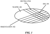
- FIGURE 1 illustrates a perspective view of a semiconductor wafer in an aspect of the present disclosure.
- a wafer 100 may be a semiconductor wafer, or may be a substrate material with one or more layers of semiconductor material on a surface of the wafer 100.
- the wafer 100 may be grown from a seed crystal using the Czochralski process, where the seed crystal is dipped into a molten bath of semiconductor material and slowly rotated and removed from the bath. The molten material then crystalizes onto the seed crystal in the orientation of the crystal.
- the wafer 100 may be a compound material, such as gallium arsenide (GaAs) or gallium nitride (GaN), a ternary material such as indium gallium arsenide (InGaAs), quaternary materials, or any material that can be a substrate material for other semiconductor materials. Although many of the materials may be crystalline in nature, polycrystalline or amorphous materials may also be used for the wafer 100.
- the wafer 100 may be supplied with materials that make the wafer 100 more conductive.
- a silicon wafer may have phosphorus or boron added to the wafer 100 to allow for electrical charge to flow in the wafer 100.
- These additives are referred to as dopants, and provide extra charge carriers (either electrons or holes) within the wafer 100 or portions of the wafer 100.
- the wafer 100 has an orientation 102 that indicates the crystalline orientation of the wafer 100.
- the orientation 102 may be a flat edge of the wafer 100 as shown in FIGURE 1 , or may be a notch or other indicia to illustrate the crystalline orientation of the wafer 100.
- the orientation 102 may indicate the Miller Indices for the planes of the crystal lattice in the wafer 100.
- the Miller Indices form a notation system of the crystallographic planes in crystal lattices.
- the lattice planes may be indicated by three integers h, k, and l, which are the Miller indices for a plane (hkf) in the crystal. Each index denotes a plane orthogonal to a direction (h, k, l) in the basis of the reciprocal lattice vectors.
- the integers are usually written in lowest terms (e.g., their greatest common divisor should be 1).
- Miller index 100 represents a plane orthogonal to direction h; index 010 represents a plane orthogonal to direction k, and index 001 represents a plane orthogonal to l.
- negative numbers are used (written as a bar over the index number) and for some crystals, such as gallium nitride, more than three numbers may be employed to adequately describe the different crystallographic planes.
- the wafer 100 is divided up along dicing lines 104.
- the dicing lines 104 indicate where the wafer 100 is to be broken apart or separated into pieces.
- the dicing lines 104 may define the outline of the various integrated circuits that have been fabricated on the wafer 100.
- the wafer 100 may be sawn or otherwise separated into pieces to form die 106.
- Each of the die 106 may be an integrated circuit with many devices or may be a single electronic device.
- the physical size of the die 106 which may also be referred to as a chip or a semiconductor chip, depends at least in part on the ability to separate the wafer 100 into certain sizes, as well as the number of individual devices that the die 106 is designed to contain.
- the die 106 may be mounted into packaging to allow access to the devices and/or integrated circuits fabricated on the die 106.
- Packaging may include single in-line packaging, dual in-line packaging, motherboard packaging, flip-chip packaging, indium dot/bump packaging, or other types of devices that provide access to the die 106.
- the die 106 may also be directly accessed through wire bonding, probes, or other connections without mounting the die 106 into a separate package.
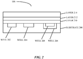
- FIGURE 2 illustrates a cross-sectional view of a die 106 in accordance with an aspect of the present disclosure.
- a substrate 200 which may be a semiconductor material and/or may act as a mechanical support for electronic devices.
- the substrate 200 may be a doped semiconductor substrate, which has either electrons (designated N-channel) or holes (designated P-channel) charge carriers present throughout the substrate 200. Subsequent doping of the substrate 200 with charge carrier ions/atoms may change the charge carrying capabilities of the substrate 200.
- a substrate 200 there may be wells 202 and 204, which may be the source and/or drain of a field-effect transistor (FET), or wells 202 and/or 204 may be fin structures of a fin structured FET (FinFET).
- Wells 202 and/or 204 may also be other devices (e.g., a resistor, a capacitor, a diode, or other electronic devices) depending on the structure and other characteristics of the wells 202 and/or 204 and the surrounding structure of the substrate 200.
- the semiconductor substrate may also have a well 206 and a well 208.
- the well 208 may be completely within the well 206, and, in some cases, may form a bipolar junction transistor (BJT).
- BJT bipolar junction transistor
- the well 206 may also be used as an isolation well to isolate the well 208 from electric and/or magnetic fields within the die 106.
- Layers may be added to the die 106.
- the layer 210 may be, for example, an oxide or insulating layer that may isolate the wells (e.g., 202-208) from each other or from other devices on the die 106.
- the layer 210 may be silicon dioxide, a polymer, a dielectric, or another electrically insulating layer.
- the layer 210 may also be an interconnection layer, in which case it may comprise a conductive material such as copper, tungsten, aluminum, an alloy, or other conductive or metallic materials.
- the layer 212 may also be a dielectric or conductive layer, depending on the desired device characteristics and/or the materials of the layers (e.g., 210 and 214).
- the layer 214 may be an encapsulating layer, which may protect the layers (e.g., 210 and 212), as well as the wells 202-208 and the substrate 200, from external forces.
- the layer 214 may be a layer that protects the die 106 from mechanical damage, or the layer 214 may be a layer of material that protects the die 106 from electromagnetic or radiation damage.
- Electronic devices designed on the die 106 may comprise many features or structural components.
- the die 106 may be exposed to any number of methods to impart dopants into the substrate 200, the wells 202-208, and, if desired, the layers (e.g., 210-214).
- the die 106 may be exposed to ion implantation, deposition of dopant atoms that are driven into a crystalline lattice through a diffusion process, chemical vapor deposition, epitaxial growth, or other methods.
- the substrate 200, the wells 202-208, and the layers may be selectively removed or added through various processes.
- Chemical wet etching, chemical mechanical planarization (CMP), plasma etching, photoresist masking, damascene processes, and other methods may create the structures and devices of the present disclosure.
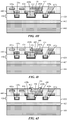
- FIGURE 3 illustrate a high density fan out (HDFO) package structure 300 according to one aspect of the present disclosure.
- the HDFO package structure 300 may couple a first conductive interconnect 350 (e.g., back-side) to an active die 302 through a second conductive interconnect 310 (e.g., front-side).
- the second conductive interconnect 310 has a pillar shape and includes a first conductive portion 304 (e.g., a conductive trace or contact pad), a second conductive portion 306 (e.g., a solder material) and a third conductive portion 308 (e.g., a conductive pillar of the active die 302).
- the second conductive interconnect may be fabricated using a conductive bump (e.g., a solder material).
- the HDFO package structure 300 also includes a contact layer 320 having a conductive interconnect layer 330 (330a, 330b, 330c) formed between one or more dielectric layers (e.g., nitride).
- the HDFO package structure 300 also includes a redistribution layer 340 including conductive routing layers (e.g., 342, 344, 346) coupled to the first conductive interconnect 350 through, for example, an under fill interconnect layer 348.
- the conductive routing layers (e.g., 342, 344, 346) of the redistribution layer 340 in combination with the conductive interconnect layer 330 (e.g., 330a, 330b, 330c) of the contact layer 320 facilitate communication between the active die 302 and the first conductive interconnect 350 (e.g., a ball grid array (BGA)).
- the conductive interconnect layer 330 is formed using a first back-end-of -line (BEOL) conductive interconnect layer (e.g., metal one (M1)).
- BEOL back-end-of -line
- M1 metal one
- the conductive interconnect layer 330 may be surrounded by dielectric layers of the contact layer 320 and coupled to the second conductive interconnect 310 through a first via 322 (e.g., a middle-of-line (MOL) zero via (V0)).
- a first via 322 e.g., a middle-of-line (MOL) zero via (V0)
- the conductive interconnect layer 330 (e.g., 330b) is coupled to the redistribution layer 340 through a second via 324 (e.g., a BEOL first via (VI) or a conductive trace) and coupled to the active die 302 through the first via 322.
- the first via 322 may be formed by a damascene process, an additive etch and fill process, a laser via and fill process or other like process for via formation.
- the second via 324 may be a conductive routing layer of the redistribution layer 340.
- the conductive routing layers (e.g., 342, 344, 346) may be formed within a polymer dielectric material of the redistribution layer 340.
- the conductive interconnect layer 330 and the conductive routing layers (e.g., 342, 344, 346) may be composed of copper or other suitable conductive material.
- portions (e.g., 330a, 330b, 330c) of the conductive interconnect layer 330 are partially surrounded by a barrier liner 332 (e.g., 332a, 332b, 332c).
- the barrier liner 332 may be disposed on sidewalls and a first surface of the conductive interconnect layer 330 that faces the active die 302.
- the barrier liner 332 is not on a second surface of the conductive interconnect layer 330 that faces the redistribution layer 340 and faces away from the active die 302.
- the barrier liner 332 may be provided by the foundry during the fabrication process of the conductive interconnect layer 330.
- barrier liner 332 may be formed during the fabrication of the HDFO package structure 300, the barrier liner 332 may be formed prior to the fabrication of the HDFO package structure 300.
- the barrier liner 332 may be composed of a barrier material such a tantalum or other suitable barrier material.
- the redistribution layer 340 includes a first conductive routing layer 342 coupled to the second via 324.
- a portion (e.g., 332d) of the barrier liner 332 is disposed on sidewalls of the second via 324 and a surface of the first conductive routing layer 342 facing the active die 302.
- the first conductive routing layer 326 is formed using, for example, a second BEOL interconnect layer (e.g., metal two (M2)).
- M2 metal two
- a second conductive routing layer 346 is coupled to the first conductive routing layer 326 through a third via 344 (e.g., a second BEOL via (V2)).
- the second conductive routing layer 346 is formed using, for example, a third BEOL conductive interconnect layer (e.g., metal three (M3)).
- M3 metal three
- the second conductive routing layer 346 is also coupled to the first conductive interconnect 350 through, for example, an under fill interconnect layer 348.
- the first conductive interconnect 350 may couple to a system board, a package substrate or other suitable carrier substrate (not shown).
- the first conductive interconnect 350 may be configured according to a ball grid array (BGA) interconnect structure.
- BGA ball grid array
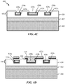
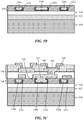
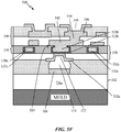
- FIGURES 4A-4M illustrate an HDFO package structure 400 at various stages of fabrication according to aspects of the present disclosure.
- FIGURES 4A-4L illustrate a sequential fabrication approach of the HDFO package structure 400 shown in FIGURE 4M .
- a carrier substrate e.g., a semiconductor wafer
- the carrier substrate 460 may be, for example, a silicon-based substrate, a glass-based substrate or other materials such as those implemented with bulk substrates for semiconductor wafers.
- An insulating layer 462 may be deposited on an active surface of the carrier substrate 460.
- the insulating layer 462 may be an oxide or other suitable insulator material.
- a first dielectric layer of a contact layer 420 may be deposited on the insulating layer 462.
- the contact layer 420 may be a passivation layer including an oxide, a nitride or other like insulator material and may insulate signals as well as protect the various circuits and the conductive elements.
- a conductive interconnect layer 430 for routing signals between a redistribution layer 440 and an active die 402 is formed by depositing a conductive material (e.g., copper) on a first dielectric layer of the contact layer 420.
- the conductive interconnect layer 430 may include conductive portions 430a, 430b and 420c.
- the conductive portions 430a, 430b and 420c may be formed using a first BEOL interconnect layer (e.g., M1).
- the conductive portions 430a, 430b and 430c are partially surrounded by a barrier liner 432 (e.g., 432a, 432b, 432c).
- the barrier liner 432 is disposed on sidewalls and a first surface of the conductive portions 430a, 430b and 430c that faces the carrier substrate 460.
- the barrier liner 432 is not disposed on a second surface of the conductive portions 430a, 430b and 430c that faces away from the carrier substrate 460.
- the barrier liner 432 e.g., tantalum
- the barrier liner 432 is provided by the foundry during the fabrication process of the conductive interconnect layer 430.
- additional dielectric layers of the contact layer 420 are deposited.
- the dielectric layers of the contact layer 420 may be composed of a nitride layer (e.g., silicon nitride (SiN)).
- a nitride layer e.g., silicon nitride (SiN)
- One or more openings 426a, 426b, 426c within the dielectric material of the contact layer 420 are formed to expose the second surface of the conductive portions 430a, 430b and 430c that is not covered by the barrier liner 432.
- the exposed portion of the conductive portions 430a, 430b and 430c may define a contact area for coupling to conductive routing layers of a redistribution layer.
- a first conductive routing layer 442 of a redistribution layer (e.g., 440 illustrated in FIGURE 4L and 4M ) is formed on the contact layer 420.
- the redistribution layer may be a backside redistribution layer (BRDL) that is formed on a full thickness wafer (e.g., the carrier substrate 460).
- the redistribution layer is formed before attaching one or more active die to the HDFO package structure 400.
- the redistribution layer may be formed on a dielectric layer of the contact layer 420. Forming the redistribution layer includes forming conductive routing layers and interconnecting the conductive routing layers by way of vias or other interconnections (e.g., conductive pads, conductive traces, etc.)
- a first conductive routing layer 442 is formed on the contact layer 420.
- the first conductive routing layer 442 may be formed using the second BEOL interconnect (e.g., M2).
- Forming the first conductive routing layer 442 includes formation of a contact to the conductive interconnect layer 430.
- a second via 424 may be formed by depositing a conductive material in one of the openings 426b and on the second surface of one of the conductive portions 430b.
- the second via 424 may be formed using the first BEOL via (VI).
- the second via 424 is formed by depositing a conductive material in the opening 450b within the contact layer 420, rather than using a process for forming a complex through silicon via.
- the first conductive routing layer 442 is formed on the second via 424 and on the barrier liner 432d on the surface of the contact layer 420.
- a first material layer (e.g., a polymer dielectric material) of a redistribution layer 440 is deposited on the contact layer 420 and on each of the portions of the first conductive routing layer 442.
- a first layer polymer dielectric is deposited on the portions of the first conductive routing layer 442.
- an opening is formed within the first material layer of the redistribution layer 440 to expose a surface of the first conductive routing layer 442.
- the first material layer of the redistribution layer 440 includes an opening 441 that exposes a contact area of the first conductive routing layer 442.
- the contact area of the first conductive routing layer 442 faces away from the carrier substrate 460.
- a second conductive routing layer 446 of the redistribution layer 440 is formed on the first material layer of the redistribution layer 440.
- the second conductive routing layer 446 may be formed using the second BEOL interconnect (e.g., M2) that includes conductive portions.
- Forming the second conductive routing layer 446 includes forming redistribution conductive portions on the first material layer of the redistribution layer 440.
- a contact area of the second conductive routing layer 446 is coupled to a contact area of the first conductive routing layer 442 through a third via 444.
- the third via 444 is formed in the opening 441 within the first material layer of the redistribution layer 440.
- the third via 444 may be formed as the second BEOL via (e.g., V2).
- a second material layer of the redistribution layer 440 is deposited on the first material layer of the redistribution layer 440.
- the second material layer of the redistribution layer 440 is deposited on each of the portions of the second conductive routing layer 446.
- a second layer of polymer dielectric material is deposited on each conductive portion of the second conductive routing layer 446 and on the first layer of polymer dielectric material of the redistribution layer 440.
- an opening 443 is formed within the second material layer of the redistribution layer 440 to expose a surface of the second conductive routing layer 446.
- the opening 443 exposes a contact area of the second conductive routing layer 446.
- the exposed contact area of the second conductive routing layer 446 may be prepared for connecting to external devices.
- the contact area of the second conductive routing layer 446 may be configured according to a ball grid array (BGA) interconnect structure.
- the contact area of the second conductive routing layer 446 may be configured to receive an under fill interconnect layer for connecting the ball grid array (BGA) interconnect structure to an external device.
- a conductive material may be deposited in the opening 443 to enable connection of the HDFO package structure 400 to external devices.
- an under fill interconnect layer 448 e.g., an under bump metallization (UBM) layer, seed layer, etc.
- UBM under bump metallization
- the under fill interconnect layer 448 may be configured to receive a first conductive interconnect (e.g., 450 of FIGURE 4M ) for connecting to an external device.
- the HDFO package structure 400 may be thinned to a desired thickness by removing the carrier substrate 460.
- the carrier substrate 460 and other layers e.g., insulating layer 462 and/or a portion of the dielectric layers of the contact layer 420
- the layers may be removed by a planarizing process or other processes (e.g., grinding, polishing or etching).
- the removal of the carrier substrate 460 and the insulating layer 462 exposes a surface of the contact layer 420.
- An opening 425 is formed within a dielectric layer of the contact layer 420 to expose the barrier liner portion 432b on one of the conductive portions 430b of the conductive interconnect layer 430.
- the opening 445 exposes a contact area of the barrier liner portion 432b of the barrier liner 432 that faces away from the redistribution layer 440.
- This exposed contact area may be configured to mate with an interconnect for coupling an active die to the HDFO package structure 400.
- a first via 422 is formed by depositing a conductive material (e.g., copper) in the opening 425.
- a first conductive portion 404 e.g., a conductive trace or contact pad
- a second conductive interconnect e.g., second conductive interconnect 410 of FIGURE 4M
- the first via 422 and the first conductive portion 404 may be formed by a dual damascene process.
- the first via 422 and the first conductive portion 304 may be an under fill interconnect layer (e.g., a UBM layer).
- the first conductive portion 404 may be configured to couple with a conductive pillar or other like interconnect for coupling an active die to the HDFO package structure 400, as shown in FIGURE 4M .
- an active die 402 is coupled to the HDFO package structure 400 via a second conductive interconnect 410 (e.g., front-side).
- the second conductive interconnect 410 has a pillar shape and includes a first conductive portion 304 (e.g., a conductive trace or contact pad), a second conductive portion 306 (e.g., a solder material) and a third conductive portion 308 (e.g., a conductive pillar of the active die 302).
- the combination of the first conductive portion 404, the second conductive portion 406 and the third conductive portion 408 form a conductive pillar interconnect between the active die 402 and the HDFO package structure 400.
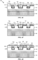
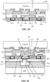
- FIGURES 5A-5F illustrate another HDFO package structure 500 at various stages of fabrication according to aspects of the present disclosure. Similar to FIGURES 4A-4M , FIGURES 5A-5F illustrate a sequential process for fabrication of the HDFO package structure 500.
- a first carrier substrate e.g., a semiconductor wafer
- An insulating layer 562 may be deposited on a surface 544 of the first carrier substrate 560.
- a first dielectric layer of a contact layer 520 may be deposited on the insulating layer 562.
- the first dielectric layer of the contact layer 520 may be a passivation layer including an oxide, a nitride or other like insulator material and may insulate signals as well as protect the various circuits and the conductive elements.
- a conductive interconnect layer 530 for routing signals between a redistribution layer and an active die is deposited on the first dielectric layer of the contact layer 520.
- the conductive interconnect layer 530 may be a first BEOL interconnect layer (e.g., M1) that includes conductive portions.
- a second dielectric layer of the contact layer 520 is deposited on the first dielectric layer and on the conductive interconnect layer 530.
- the conductive portions 520a, 520b and 520c may be partially surrounded by a barrier liner 532 (532a, 532b, 532c).
- the barrier liner 532 (e.g., from the foundry) may be tantalum or other suitable barrier materials.
- FIGURE 5C illustrates a redistribution layer 540 formed on the contact layer 520 and coupled to a conductive portion 530b of the conductive interconnect layer 530.
- the redistribution layer 540 is formed before attaching one or more active die to the HDFO package structure 500.
- Forming the redistribution layer 540 includes forming conductive routing layers (e.g., 542, 546) and interconnecting the conductive routing layers (e.g., 542, 546) by way of vias (e.g., 524, 544) or other like interconnections.
- a first conductive routing layer 542 (e.g., M2) is formed on the contact layer 520 and coupled to the conductive portion 530b of the conductive interconnect layer 530 using a second via 524 (e.g., V1).
- a second conductive routing layer 546 (e.g., M3) is formed on a first polymer dielectric layer and coupled to the first conductive routing layer 526 using a third via 524 (e.g., V2).
- a contact area of the second conductive routing layer 546 may be coupled to a conductive interconnect for connecting the HDFO package structure 500 to one or more external devices.
- the contact area of the second conductive routing layer 546 may be configured according to a ball grid array (BGA) interconnect structure.
- the contact area of the second conductive routing layer 546 may be configured to receive a solder interconnect for connecting the ball grid array (BGA) interconnect structure to the one or more external devices.
- an under fill interconnect layer 548 (e.g., a backside UBM layer) is deposited on the contact area of the second conductive routing layer 546.
- the under fill interconnect layer 548 may be deposited on the contact area of the second conductive routing layer 546.
- a second carrier substrate 570 may be attached to the HDFO package structure 500 (as shown in FIGURE 5D ) to perform the remaining processes.
- layers of the HDFO package structure 500 are removed to bring the HDFO package structure 500 to a desired thickness.
- the layers of the HDFO package structure 500 are removed with the support of the second carrier substrate 570.
- the second carrier substrate 570 provides support for the HDFO package structure 500 while removing the layers.
- the second carrier substrate 570 may be attached to exposed surfaces of the HDFO package structure 500 opposite the first carrier substrate 560 that was removed.
- the second carrier substrate 570 may be configured to provide structural rigidity or a base for removal of the first carrier substrate 560 and other layers (e.g., insulating layer 562 and a dielectric layer of the contact layer 520).
- the layers may be removed by a planarizing process or other like processes (e.g., grinding, polishing or etching).
- removal of the layers may include removal of the first carrier substrate 560 and the insulating layer 562 to expose the surface of the contact layer 520 as shown in FIGURE 5E .
- an active die 502 is coupled to the HDFO package structure 500 by one or more interconnects.
- a first via 522 (e.g., V0) is formed within the contact layer 520.
- the first via 522 may be lined with a seed layer or an under fill interconnect layer 504.
- the first via 522 is aligned to a second conductive interconnect 510 for coupling the active die to the HDFO package structure 500.
- a solder material may be deposited on the under fill interconnect layer 504 to couple with a contact pad 508 for coupling the active die 502 to the HDFO package structure 500.
- a mold material 580 is coupled to a surface of the active die 502 opposite the redistribution layer 540. It should be recognized that an HDFO package structure, according to aspects of the present disclosure, is not limited to the number of layers shown in FIGURES 4A-4M and 5A to 5F .
- FIGURE 6 is a flow diagram illustrating a method 600 for fabricating a high density fan out (HDFO) package structure according to one aspect of the disclosure.
- a contact layer is fabricated on a carrier substrate.
- the contact layer include a conductive interconnect layer having a barrier liner on a first surface, for example, as shown in FIGURES 3 and 4M .
- a redistribution layer is fabricated.
- the RDL includes conductive routing layers configured to couple a first conductive interconnect to the conductive interconnect layer.
- a conductive material is deposited within an opening in the contact layer to form a first via on the barrier liner after removing the carrier substrate.
- the first via 422 is formed after removing the carrier substrate 460.
- an active die is attached to the via using a second conductive interconnect.
- the barrier liner 432 on the first surface of the conductive interconnect layer 430 faces the active die 402, for example, as shown in FIGURE 4M .
- a high density fan out package (HDFO) package structure includes means for coupling a first conductive interconnect to a conductive interconnect layer.
- a second surface of the conductive interconnect layer faces the coupling means and a first surface of the conductive interconnect layer faces an active die.
- the coupling means is the redistribution layer 440/550 of FIGURES 4M and 5F , configured to perform the functions recited by the coupling means.
- the aforementioned means may be a device or any layer configured to perform the functions recited by the aforementioned means.
- a HDFO package structure includes multiple active die or a single chip structure.
- the HDFO package structure may be fabricated according to a chip last attach process.
- the chip last attach process includes attaching an active die to the HDFO package structure after a redistribution layer is formed. For example, the redistribution layer may be verified through testing before the active die is attached to avoid attachment to a defective redistribution layer.
- the HDFO package structure includes a contact layer that includes a conductive interconnect layer.
- the conductive interconnect layer may include a first surface facing an active die and a second surface facing a redistribution layer.
- a first conductive interconnect (e.g., ball grid array (BGA)) may couple the HDFO package structure to an external device.
- a conductive liner may be disposed on the first surface of the conductive interconnect layer.
- the conductive liner may be a barrier or seed liner of tantalum. The barrier liner may provide protection for the conductive interconnect layer during the formation (e.g., electroplating) of the interconnects to the active die.
- a redistribution layer is coupled to the conductive interconnect layer of the contact layer.
- the redistribution layer may be a fan out routing layer.
- the redistribution layer includes conductive routing layers configured to couple a first conductive interconnect to the conductive interconnect layer.
- the redistribution layer is formed before attaching the active die to avoid damaging the active die during formation of the redistribution layer.
- the redistribution layer can be a backside redistribution layer (BRDL) that is formed on a full thickness wafer. Implementing the HDFO package structure on the backside redistribution layer improves yield of the active die and reduces warpage of the HDFO package structure.
- a via may be coupled to the barrier liner to interconnect the second conductive interconnect of the active die.
- the conductive material may include one or more conductive interconnects.
- the second conductive material may include an under bump conductive interconnect, a solder material and/or a conductive pillar.
- the under bump conductive interconnect may be disposed in an opening within the conductive layer that exposes a surface of the barrier liner.
- the conductive pillar may be coupled to a contact pad of the die.
- the solder material be between the under bump conductive interconnect and the conductive pillar.
- the under bump conductive interconnect and the conductive pillar may be copper.
- FIGURE 7 is a block diagram showing an exemplary wireless communication system 700 in which an aspect of the disclosure may be advantageously employed.
- FIGURE 7 shows three remote units 720, 730, and 750 and two base stations 740.
- Remote units 720, 730, and 750 include IC devices 725A, 725C, and 725B that include the disclosed HDFO package structure. It will be recognized that other devices may also include the disclosed HDFO package structure, such as the base stations, switching devices, and network equipment.
- FIGURE 7 shows forward link signals 780 from the base station 740 to the remote units 720, 730, and 750 and reverse link signals 790 from the remote units 720, 730, and 750 to base stations 740.
- remote unit 720 is shown as a mobile telephone
- remote unit 730 is shown as a portable computer
- remote unit 750 is shown as a fixed location remote unit in a wireless local loop system.
- the remote units 720, 730, and 750 may be a mobile phone, a hand-held personal communication system (PCS) unit, a communications device, a portable data unit such as a personal digital assistant (PDA), a GPS enabled device, a navigation device, a set top box, a music player, a video player, an entertainment unit, a fixed location data unit such as a meter reading equipment, or other devices that store or retrieve data or computer instructions, or combinations thereof.
- FIGURE 7 illustrates remote units according to the aspects of the disclosure, the disclosure is not limited to these exemplary illustrated units. Aspects of the disclosure may be suitably employed in many devices, which include the disclosed devices.
- FIGURE 8 is a block diagram illustrating a design workstation used for circuit, layout, and logic design of a semiconductor component, such as the devices disclosed above.
- a design workstation 800 includes a hard disk 802 containing operating system software, support files, and design software such as Cadence or OrCAD.
- the design workstation 800 also includes a display 804 to facilitate design of a circuit 806 or a semiconductor component 808 such as a HDFO package structure.
- a storage medium 810 is provided for tangibly storing the design of the circuit 806 or the semiconductor component 808.
- the design of the circuit 806 or the semiconductor component 808 may be stored on the storage medium 810 in a file format such as GDSII or GERBER.
- the storage medium 810 may be a CD-ROM, DVD, hard disk, flash memory, or other appropriate device.
- the design workstation 800 includes a drive apparatus 812 for accepting input from or writing output to the storage medium 810.
- Data recorded on the storage medium 810 may specify logic circuit configurations, pattern data for photolithography masks, or mask pattern data for serial write tools such as electron beam lithography.
- the data may further include logic verification data such as timing diagrams or net circuits associated with logic simulations.
- Providing data on the storage medium 810 facilitates the design of the circuit 806 or the semiconductor component 808 by decreasing the number of processes for designing semiconductor wafers.
- the methodologies may be implemented with modules (e.g., procedures, functions, and so on) that perform the functions described herein.
- a machine-readable medium tangibly embodying instructions may be used in implementing the methodologies described herein.
- software codes may be stored in a memory and executed by a processor unit.
- Memory may be implemented within the processor unit or external to the processor unit.
- the term "memory" refers to types of long term, short term, volatile, nonvolatile, or other memory and is not to be limited to a particular type of memory or number of memories, or type of media upon which memory is stored.
- the functions may be stored as one or more instructions or code on a computer-readable medium. Examples include computer-readable media encoded with a data structure and computer-readable media encoded with a computer program.
- Computer-readable media includes physical computer storage media. A storage medium may be an available medium that can be accessed by a computer.
- such computer-readable media can include RAM, ROM, EEPROM, CD-ROM or other optical disk storage, magnetic disk storage or other magnetic storage devices, or other medium that can be used to store desired program code in the form of instructions or data structures and that can be accessed by a computer; disk and disc, as used herein, includes compact disc (CD), laser disc, optical disc, digital versatile disc (DVD) and Blu-ray disc where disks usually reproduce data magnetically, while discs reproduce data optically with lasers. Combinations of the above should also be included within the scope of computer-readable media.
- instructions and/or data may be provided as signals on transmission media included in a communication apparatus.
- a communication apparatus may include a transceiver having signals indicative of instructions and data. The instructions and data are configured to cause one or more processors to implement the functions outlined in the claims.
- DSP digital signal processor
- ASIC application specific integrated circuit
- FPGA field programmable gate array
- a general-purpose processor may be a microprocessor, but in the alternative, the processor may be any conventional processor, controller, microcontroller, or state machine.
- a processor may also be implemented as a combination of computing devices, e.g., a combination of a DSP and a microprocessor, multiple microprocessors, one or more microprocessors in conjunction with a DSP core, or any other such configuration.
- a software module may reside in RAM, flash memory, ROM, EPROM, EEPROM, registers, hard disk, a removable disk, a CD-ROM, or any other form of storage medium known in the art.
- An exemplary storage medium is coupled to the processor such that the processor can read information from, and write information to, the storage medium.
- the storage medium may be integral to the processor.
- the processor and the storage medium may reside in an ASIC.
- the ASIC may reside in a user terminal.
- the processor and the storage medium may reside as discrete components in a user terminal.
- the functions described may be implemented in hardware, software, firmware, or any combination thereof. If implemented in software, the functions may be stored on or transmitted over as one or more instructions or code on a computer-readable medium.
- Computer-readable media includes both computer storage media and communication media including any medium that facilitates transfer of a computer program from one place to another.
- a storage media may be any available media that can be accessed by a general purpose or special purpose computer.
- such computer-readable media can include RAM, ROM, EEPROM, CD-ROM or other optical disk storage, magnetic disk storage or other magnetic storage devices, or any other medium that can be used to carry or store specified program code means in the form of instructions or data structures and that can be accessed by a general-purpose or special-purpose computer, or a general-purpose or special-purpose processor. Also, any connection is properly termed a computer-readable medium.
- Disk and disc includes compact disc (CD), laser disc, optical disc, digital versatile disc (DVD) and Blu-ray disc where disks usually reproduce data magnetically, while discs reproduce data optically with lasers. Combinations of the above should also be included within the scope of computer-readable media.
Landscapes
- Engineering & Computer Science (AREA)
- Power Engineering (AREA)
- Computer Hardware Design (AREA)
- Microelectronics & Electronic Packaging (AREA)
- Physics & Mathematics (AREA)
- General Physics & Mathematics (AREA)
- Condensed Matter Physics & Semiconductors (AREA)
- Manufacturing & Machinery (AREA)
- Ceramic Engineering (AREA)
- Geometry (AREA)
- Internal Circuitry In Semiconductor Integrated Circuit Devices (AREA)
- Wire Bonding (AREA)
- Linear Motors (AREA)
- Packages (AREA)
Applications Claiming Priority (3)
| Application Number | Priority Date | Filing Date | Title |
|---|---|---|---|
| US201462073804P | 2014-10-31 | 2014-10-31 | |
| US14/693,820 US10157823B2 (en) | 2014-10-31 | 2015-04-22 | High density fan out package structure |
| PCT/US2015/048514 WO2016069112A1 (en) | 2014-10-31 | 2015-09-04 | High density fan out package structure |
Publications (2)
| Publication Number | Publication Date |
|---|---|
| EP3213345A1 EP3213345A1 (en) | 2017-09-06 |
| EP3213345B1 true EP3213345B1 (en) | 2021-01-13 |
Family
ID=55853498
Family Applications (1)
| Application Number | Title | Priority Date | Filing Date |
|---|---|---|---|
| EP15767632.1A Active EP3213345B1 (en) | 2014-10-31 | 2015-09-04 | High density fan out package structure |
Country Status (8)
Families Citing this family (22)
| Publication number | Priority date | Publication date | Assignee | Title |
|---|---|---|---|---|
| US9728507B2 (en) * | 2011-07-19 | 2017-08-08 | Pfg Ip Llc | Cap chip and reroute layer for stacked microelectronic module |
| US20170047276A1 (en) * | 2015-08-13 | 2017-02-16 | Advanced Semiconductor Engineering, Inc. | Semiconductor device package and method of manufacturing the same |
| US9761509B2 (en) | 2015-12-29 | 2017-09-12 | United Microelectronics Corp. | Semiconductor device with throgh-substrate via and method for fabrication the semiconductor device |
| US10141198B2 (en) * | 2016-07-08 | 2018-11-27 | Dyi-chung Hu | Electronic package and manufacturing method thereof |
| US10872872B2 (en) | 2016-12-30 | 2020-12-22 | Intel Corporation | Package substrate with high-density interconnect layer having pillar and via connections for fan out scaling |
| US10050021B1 (en) * | 2017-02-16 | 2018-08-14 | Nanya Technology Corporation | Die device, semiconductor device and method for making the same |
| TWI699840B (zh) * | 2017-10-23 | 2020-07-21 | 美商應用材料股份有限公司 | 形成扇出互連結構與互連結構的方法 |
| DE102018127448B4 (de) | 2017-11-30 | 2023-06-22 | Taiwan Semiconductor Manufacturing Co. Ltd. | Metallschienenleiter für nicht-planare Halbleiter-Bauelemente |
| US10700207B2 (en) | 2017-11-30 | 2020-06-30 | Taiwan Semiconductor Manufacturing Company Ltd. | Semiconductor device integrating backside power grid and related integrated circuit and fabrication method |
| US10804254B2 (en) | 2018-06-29 | 2020-10-13 | Taiwan Semiconductor Manufacturing Company, Ltd. | Fan-out package with cavity substrate |
| US20200212536A1 (en) * | 2018-12-31 | 2020-07-02 | Texas Instruments Incorporated | Wireless communication device with antenna on package |
| JP7335036B2 (ja) * | 2019-03-29 | 2023-08-29 | ラピスセミコンダクタ株式会社 | 半導体パッケージの製造方法 |
| KR102615198B1 (ko) | 2019-10-15 | 2023-12-18 | 삼성전자주식회사 | 반도체 패키지 |
| KR102765303B1 (ko) | 2019-12-31 | 2025-02-07 | 삼성전자주식회사 | 반도체 패키지 |
| US11356070B2 (en) | 2020-06-01 | 2022-06-07 | Wolfspeed, Inc. | RF amplifiers having shielded transmission line structures |
| US12166003B2 (en) * | 2020-04-03 | 2024-12-10 | Macom Technology Solutions Holdings, Inc. | RF amplifier devices including top side contacts and methods of manufacturing |
| US11302662B2 (en) * | 2020-05-01 | 2022-04-12 | Nanya Technology Corporation | Semiconductor package with air gap and manufacturing method thereof |
| CN114743942A (zh) * | 2021-01-07 | 2022-07-12 | 联华电子股份有限公司 | 混合式接合结构及其制作方法 |
| KR20220126850A (ko) | 2021-03-09 | 2022-09-19 | 삼성전자주식회사 | 반도체 패키지 |
| CN117546291A (zh) * | 2021-06-11 | 2024-02-09 | 株式会社村田制作所 | 半导体装置 |
| US12148688B2 (en) | 2023-02-13 | 2024-11-19 | Dyi-chung Hu | Semiconductor substrate and manufacturing method thereof |
| TWI884561B (zh) * | 2023-02-13 | 2025-05-21 | 胡迪群 | 半導體基板及其製造方法 |
Family Cites Families (14)
| Publication number | Priority date | Publication date | Assignee | Title |
|---|---|---|---|---|
| US6706625B1 (en) * | 2002-12-06 | 2004-03-16 | Chartered Semiconductor Manufacturing Ltd. | Copper recess formation using chemical process for fabricating barrier cap for lines and vias |
| US6927159B2 (en) * | 2003-05-27 | 2005-08-09 | Texas Instruments Incorporated | Methods for providing improved layer adhesion in a semiconductor device |
| TWI286372B (en) | 2003-08-13 | 2007-09-01 | Phoenix Prec Technology Corp | Semiconductor package substrate with protective metal layer on pads formed thereon and method for fabricating the same |
| US9460951B2 (en) * | 2007-12-03 | 2016-10-04 | STATS ChipPAC Pte. Ltd. | Semiconductor device and method of wafer level package integration |
| US8513119B2 (en) * | 2008-12-10 | 2013-08-20 | Taiwan Semiconductor Manufacturing Company, Ltd. | Method of forming bump structure having tapered sidewalls for stacked dies |
| US8441124B2 (en) * | 2010-04-29 | 2013-05-14 | Taiwan Semiconductor Manufacturing Company, Ltd. | Cu pillar bump with non-metal sidewall protection structure |
| US20120282767A1 (en) | 2011-05-05 | 2012-11-08 | Stmicroelectronics Pte Ltd. | Method for producing a two-sided fan-out wafer level package with electrically conductive interconnects, and a corresponding semiconductor package |
| KR101828490B1 (ko) | 2011-08-30 | 2018-02-12 | 삼성전자주식회사 | 관통전극을 갖는 반도체 소자 및 그 제조방법 |
| US8552556B1 (en) | 2011-11-22 | 2013-10-08 | Amkor Technology, Inc. | Wafer level fan out package |
| US8779559B2 (en) * | 2012-02-27 | 2014-07-15 | Qualcomm Incorporated | Structure and method for strain-relieved TSV |
| US9385006B2 (en) * | 2012-06-21 | 2016-07-05 | STATS ChipPAC Pte. Ltd. | Semiconductor device and method of forming an embedded SOP fan-out package |
| KR20140024674A (ko) * | 2012-08-20 | 2014-03-03 | 삼성전자주식회사 | 관통 비아 구조체 및 재배선 구조체를 갖는 반도체 소자 |
| US9006101B2 (en) | 2012-08-31 | 2015-04-14 | Taiwan Semiconductor Manufacturing Company, Ltd. | Interconnect structure and method |
| US8993380B2 (en) | 2013-03-08 | 2015-03-31 | Taiwan Semiconductor Manufacturing Company, Ltd. | Structure and method for 3D IC package |
-
2015
- 2015-04-22 US US14/693,820 patent/US10157823B2/en active Active
- 2015-09-04 BR BR112017008727-8A patent/BR112017008727B1/pt active IP Right Grant
- 2015-09-04 KR KR1020177011236A patent/KR102440270B1/ko active Active
- 2015-09-04 CN CN201580058661.2A patent/CN107078119B/zh active Active
- 2015-09-04 SG SG11201701990SA patent/SG11201701990SA/en unknown
- 2015-09-04 JP JP2017521532A patent/JP6672285B2/ja active Active
- 2015-09-04 EP EP15767632.1A patent/EP3213345B1/en active Active
- 2015-09-04 WO PCT/US2015/048514 patent/WO2016069112A1/en active Application Filing
Non-Patent Citations (1)
| Title |
|---|
| None * |
Also Published As
| Publication number | Publication date |
|---|---|
| KR20170077133A (ko) | 2017-07-05 |
| US20160126173A1 (en) | 2016-05-05 |
| KR102440270B1 (ko) | 2022-09-02 |
| CN107078119A (zh) | 2017-08-18 |
| SG11201701990SA (en) | 2017-05-30 |
| BR112017008727B1 (pt) | 2022-06-28 |
| JP2017534177A (ja) | 2017-11-16 |
| CN107078119B (zh) | 2021-05-14 |
| US10157823B2 (en) | 2018-12-18 |
| EP3213345A1 (en) | 2017-09-06 |
| BR112017008727A2 (pt) | 2017-12-19 |
| JP6672285B2 (ja) | 2020-03-25 |
| WO2016069112A1 (en) | 2016-05-06 |
Similar Documents
| Publication | Publication Date | Title |
|---|---|---|
| EP3213345B1 (en) | High density fan out package structure | |
| US9443824B1 (en) | Cavity bridge connection for die split architecture | |
| US9583462B2 (en) | Damascene re-distribution layer (RDL) in fan out split die application | |
| US9472425B2 (en) | Power distribution improvement using pseudo-ESR control of an embedded passive capacitor | |
| US20180315672A1 (en) | Sacrificial test pads for inline test access | |
| US9496181B2 (en) | Sub-fin device isolation | |
| US10833017B2 (en) | Contact for semiconductor device | |
| US20200066630A1 (en) | Structure and method of metal wraparound for low via resistance | |
| US9966426B2 (en) | Augmented capacitor structure for high quality (Q)-factor radio frequency (RF) applications | |
| US10566413B2 (en) | MIM capacitor containing negative capacitance material | |
| WO2025090206A1 (en) | Bottom channel trench isolated gate all around (gaa) field effect transistor (fet) | |
| US20160365196A1 (en) | Capacitor structure for power delivery applications | |
| US9984029B2 (en) | Variable interconnect pitch for improved performance | |
| US20250210438A1 (en) | Method and apparatus for ambient temperature sensor design in a complementary metal oxide semiconductor (cmos) process | |
| HK1240396A1 (en) | High density fan out package structure | |
| US20250151346A1 (en) | Diode structure for direct backside contact, backside power delivery network | |
| HK1240396B (zh) | 高密度扇出封装结构 | |
| US20250207987A1 (en) | Pressure/strain sensor design in a complementary metal oxide semiconductor (cmos) process |
Legal Events
| Date | Code | Title | Description |
|---|---|---|---|
| STAA | Information on the status of an ep patent application or granted ep patent |
Free format text: STATUS: THE INTERNATIONAL PUBLICATION HAS BEEN MADE |
|
| PUAI | Public reference made under article 153(3) epc to a published international application that has entered the european phase |
Free format text: ORIGINAL CODE: 0009012 |
|
| STAA | Information on the status of an ep patent application or granted ep patent |
Free format text: STATUS: REQUEST FOR EXAMINATION WAS MADE |
|
| 17P | Request for examination filed |
Effective date: 20170314 |
|
| AK | Designated contracting states |
Kind code of ref document: A1 Designated state(s): AL AT BE BG CH CY CZ DE DK EE ES FI FR GB GR HR HU IE IS IT LI LT LU LV MC MK MT NL NO PL PT RO RS SE SI SK SM TR |
|
| AX | Request for extension of the european patent |
Extension state: BA ME |
|
| DAV | Request for validation of the european patent (deleted) | ||
| DAX | Request for extension of the european patent (deleted) | ||
| GRAP | Despatch of communication of intention to grant a patent |
Free format text: ORIGINAL CODE: EPIDOSNIGR1 |
|
| STAA | Information on the status of an ep patent application or granted ep patent |
Free format text: STATUS: GRANT OF PATENT IS INTENDED |
|
| INTG | Intention to grant announced |
Effective date: 20200731 |
|
| GRAS | Grant fee paid |
Free format text: ORIGINAL CODE: EPIDOSNIGR3 |
|
| GRAA | (expected) grant |
Free format text: ORIGINAL CODE: 0009210 |
|
| STAA | Information on the status of an ep patent application or granted ep patent |
Free format text: STATUS: THE PATENT HAS BEEN GRANTED |
|
| AK | Designated contracting states |
Kind code of ref document: B1 Designated state(s): AL AT BE BG CH CY CZ DE DK EE ES FI FR GB GR HR HU IE IS IT LI LT LU LV MC MK MT NL NO PL PT RO RS SE SI SK SM TR |
|
| REG | Reference to a national code |
Ref country code: GB Ref legal event code: FG4D |
|
| REG | Reference to a national code |
Ref country code: CH Ref legal event code: EP |
|
| REG | Reference to a national code |
Ref country code: IE Ref legal event code: FG4D |
|
| REG | Reference to a national code |
Ref country code: DE Ref legal event code: R096 Ref document number: 602015064754 Country of ref document: DE |
|
| REG | Reference to a national code |
Ref country code: AT Ref legal event code: REF Ref document number: 1355179 Country of ref document: AT Kind code of ref document: T Effective date: 20210215 |
|
| REG | Reference to a national code |
Ref country code: NL Ref legal event code: FP |
|
| REG | Reference to a national code |
Ref country code: AT Ref legal event code: MK05 Ref document number: 1355179 Country of ref document: AT Kind code of ref document: T Effective date: 20210113 |
|
| REG | Reference to a national code |
Ref country code: LT Ref legal event code: MG9D |
|
| PG25 | Lapsed in a contracting state [announced via postgrant information from national office to epo] |
Ref country code: LT Free format text: LAPSE BECAUSE OF FAILURE TO SUBMIT A TRANSLATION OF THE DESCRIPTION OR TO PAY THE FEE WITHIN THE PRESCRIBED TIME-LIMIT Effective date: 20210113 Ref country code: PT Free format text: LAPSE BECAUSE OF FAILURE TO SUBMIT A TRANSLATION OF THE DESCRIPTION OR TO PAY THE FEE WITHIN THE PRESCRIBED TIME-LIMIT Effective date: 20210513 Ref country code: HR Free format text: LAPSE BECAUSE OF FAILURE TO SUBMIT A TRANSLATION OF THE DESCRIPTION OR TO PAY THE FEE WITHIN THE PRESCRIBED TIME-LIMIT Effective date: 20210113 Ref country code: FI Free format text: LAPSE BECAUSE OF FAILURE TO SUBMIT A TRANSLATION OF THE DESCRIPTION OR TO PAY THE FEE WITHIN THE PRESCRIBED TIME-LIMIT Effective date: 20210113 Ref country code: GR Free format text: LAPSE BECAUSE OF FAILURE TO SUBMIT A TRANSLATION OF THE DESCRIPTION OR TO PAY THE FEE WITHIN THE PRESCRIBED TIME-LIMIT Effective date: 20210414 Ref country code: NO Free format text: LAPSE BECAUSE OF FAILURE TO SUBMIT A TRANSLATION OF THE DESCRIPTION OR TO PAY THE FEE WITHIN THE PRESCRIBED TIME-LIMIT Effective date: 20210413 Ref country code: BG Free format text: LAPSE BECAUSE OF FAILURE TO SUBMIT A TRANSLATION OF THE DESCRIPTION OR TO PAY THE FEE WITHIN THE PRESCRIBED TIME-LIMIT Effective date: 20210413 |
|
| PG25 | Lapsed in a contracting state [announced via postgrant information from national office to epo] |
Ref country code: RS Free format text: LAPSE BECAUSE OF FAILURE TO SUBMIT A TRANSLATION OF THE DESCRIPTION OR TO PAY THE FEE WITHIN THE PRESCRIBED TIME-LIMIT Effective date: 20210113 Ref country code: PL Free format text: LAPSE BECAUSE OF FAILURE TO SUBMIT A TRANSLATION OF THE DESCRIPTION OR TO PAY THE FEE WITHIN THE PRESCRIBED TIME-LIMIT Effective date: 20210113 Ref country code: LV Free format text: LAPSE BECAUSE OF FAILURE TO SUBMIT A TRANSLATION OF THE DESCRIPTION OR TO PAY THE FEE WITHIN THE PRESCRIBED TIME-LIMIT Effective date: 20210113 Ref country code: AT Free format text: LAPSE BECAUSE OF FAILURE TO SUBMIT A TRANSLATION OF THE DESCRIPTION OR TO PAY THE FEE WITHIN THE PRESCRIBED TIME-LIMIT Effective date: 20210113 Ref country code: SE Free format text: LAPSE BECAUSE OF FAILURE TO SUBMIT A TRANSLATION OF THE DESCRIPTION OR TO PAY THE FEE WITHIN THE PRESCRIBED TIME-LIMIT Effective date: 20210113 |
|
| PG25 | Lapsed in a contracting state [announced via postgrant information from national office to epo] |
Ref country code: IS Free format text: LAPSE BECAUSE OF FAILURE TO SUBMIT A TRANSLATION OF THE DESCRIPTION OR TO PAY THE FEE WITHIN THE PRESCRIBED TIME-LIMIT Effective date: 20210513 |
|
| REG | Reference to a national code |
Ref country code: DE Ref legal event code: R097 Ref document number: 602015064754 Country of ref document: DE |
|
| PG25 | Lapsed in a contracting state [announced via postgrant information from national office to epo] |
Ref country code: SM Free format text: LAPSE BECAUSE OF FAILURE TO SUBMIT A TRANSLATION OF THE DESCRIPTION OR TO PAY THE FEE WITHIN THE PRESCRIBED TIME-LIMIT Effective date: 20210113 Ref country code: CZ Free format text: LAPSE BECAUSE OF FAILURE TO SUBMIT A TRANSLATION OF THE DESCRIPTION OR TO PAY THE FEE WITHIN THE PRESCRIBED TIME-LIMIT Effective date: 20210113 Ref country code: EE Free format text: LAPSE BECAUSE OF FAILURE TO SUBMIT A TRANSLATION OF THE DESCRIPTION OR TO PAY THE FEE WITHIN THE PRESCRIBED TIME-LIMIT Effective date: 20210113 |
|
| PLBE | No opposition filed within time limit |
Free format text: ORIGINAL CODE: 0009261 |
|
| STAA | Information on the status of an ep patent application or granted ep patent |
Free format text: STATUS: NO OPPOSITION FILED WITHIN TIME LIMIT |
|
| PG25 | Lapsed in a contracting state [announced via postgrant information from national office to epo] |
Ref country code: DK Free format text: LAPSE BECAUSE OF FAILURE TO SUBMIT A TRANSLATION OF THE DESCRIPTION OR TO PAY THE FEE WITHIN THE PRESCRIBED TIME-LIMIT Effective date: 20210113 Ref country code: RO Free format text: LAPSE BECAUSE OF FAILURE TO SUBMIT A TRANSLATION OF THE DESCRIPTION OR TO PAY THE FEE WITHIN THE PRESCRIBED TIME-LIMIT Effective date: 20210113 Ref country code: SK Free format text: LAPSE BECAUSE OF FAILURE TO SUBMIT A TRANSLATION OF THE DESCRIPTION OR TO PAY THE FEE WITHIN THE PRESCRIBED TIME-LIMIT Effective date: 20210113 |
|
| 26N | No opposition filed |
Effective date: 20211014 |
|
| PG25 | Lapsed in a contracting state [announced via postgrant information from national office to epo] |
Ref country code: ES Free format text: LAPSE BECAUSE OF FAILURE TO SUBMIT A TRANSLATION OF THE DESCRIPTION OR TO PAY THE FEE WITHIN THE PRESCRIBED TIME-LIMIT Effective date: 20210113 Ref country code: AL Free format text: LAPSE BECAUSE OF FAILURE TO SUBMIT A TRANSLATION OF THE DESCRIPTION OR TO PAY THE FEE WITHIN THE PRESCRIBED TIME-LIMIT Effective date: 20210113 |
|
| PG25 | Lapsed in a contracting state [announced via postgrant information from national office to epo] |
Ref country code: SI Free format text: LAPSE BECAUSE OF FAILURE TO SUBMIT A TRANSLATION OF THE DESCRIPTION OR TO PAY THE FEE WITHIN THE PRESCRIBED TIME-LIMIT Effective date: 20210113 |
|
| PG25 | Lapsed in a contracting state [announced via postgrant information from national office to epo] |
Ref country code: IT Free format text: LAPSE BECAUSE OF FAILURE TO SUBMIT A TRANSLATION OF THE DESCRIPTION OR TO PAY THE FEE WITHIN THE PRESCRIBED TIME-LIMIT Effective date: 20210113 |
|
| REG | Reference to a national code |
Ref country code: CH Ref legal event code: PL |
|
| REG | Reference to a national code |
Ref country code: BE Ref legal event code: MM Effective date: 20210930 |
|
| PG25 | Lapsed in a contracting state [announced via postgrant information from national office to epo] |
Ref country code: IS Free format text: LAPSE BECAUSE OF FAILURE TO SUBMIT A TRANSLATION OF THE DESCRIPTION OR TO PAY THE FEE WITHIN THE PRESCRIBED TIME-LIMIT Effective date: 20210513 Ref country code: MC Free format text: LAPSE BECAUSE OF FAILURE TO SUBMIT A TRANSLATION OF THE DESCRIPTION OR TO PAY THE FEE WITHIN THE PRESCRIBED TIME-LIMIT Effective date: 20210113 |
|
| PG25 | Lapsed in a contracting state [announced via postgrant information from national office to epo] |
Ref country code: LU Free format text: LAPSE BECAUSE OF NON-PAYMENT OF DUE FEES Effective date: 20210904 Ref country code: IE Free format text: LAPSE BECAUSE OF NON-PAYMENT OF DUE FEES Effective date: 20210904 Ref country code: BE Free format text: LAPSE BECAUSE OF NON-PAYMENT OF DUE FEES Effective date: 20210930 |
|
| PG25 | Lapsed in a contracting state [announced via postgrant information from national office to epo] |
Ref country code: LI Free format text: LAPSE BECAUSE OF NON-PAYMENT OF DUE FEES Effective date: 20210930 Ref country code: CH Free format text: LAPSE BECAUSE OF NON-PAYMENT OF DUE FEES Effective date: 20210930 |
|
| PG25 | Lapsed in a contracting state [announced via postgrant information from national office to epo] |
Ref country code: HU Free format text: LAPSE BECAUSE OF FAILURE TO SUBMIT A TRANSLATION OF THE DESCRIPTION OR TO PAY THE FEE WITHIN THE PRESCRIBED TIME-LIMIT; INVALID AB INITIO Effective date: 20150904 |
|
| PG25 | Lapsed in a contracting state [announced via postgrant information from national office to epo] |
Ref country code: CY Free format text: LAPSE BECAUSE OF FAILURE TO SUBMIT A TRANSLATION OF THE DESCRIPTION OR TO PAY THE FEE WITHIN THE PRESCRIBED TIME-LIMIT Effective date: 20210113 |
|
| PG25 | Lapsed in a contracting state [announced via postgrant information from national office to epo] |
Ref country code: MK Free format text: LAPSE BECAUSE OF FAILURE TO SUBMIT A TRANSLATION OF THE DESCRIPTION OR TO PAY THE FEE WITHIN THE PRESCRIBED TIME-LIMIT Effective date: 20210113 |
|
| PGFP | Annual fee paid to national office [announced via postgrant information from national office to epo] |
Ref country code: NL Payment date: 20240813 Year of fee payment: 10 |
|
| PG25 | Lapsed in a contracting state [announced via postgrant information from national office to epo] |
Ref country code: MT Free format text: LAPSE BECAUSE OF FAILURE TO SUBMIT A TRANSLATION OF THE DESCRIPTION OR TO PAY THE FEE WITHIN THE PRESCRIBED TIME-LIMIT Effective date: 20210113 |
|
| PGFP | Annual fee paid to national office [announced via postgrant information from national office to epo] |
Ref country code: DE Payment date: 20240808 Year of fee payment: 10 |
|
| PGFP | Annual fee paid to national office [announced via postgrant information from national office to epo] |
Ref country code: GB Payment date: 20240808 Year of fee payment: 10 |
|
| PGFP | Annual fee paid to national office [announced via postgrant information from national office to epo] |
Ref country code: FR Payment date: 20240808 Year of fee payment: 10 |