EP3210952A1 - Oxide sintered compact, oxide sputtering target, and oxide thin film - Google Patents
Oxide sintered compact, oxide sputtering target, and oxide thin film Download PDFInfo
- Publication number
- EP3210952A1 EP3210952A1 EP16755599.4A EP16755599A EP3210952A1 EP 3210952 A1 EP3210952 A1 EP 3210952A1 EP 16755599 A EP16755599 A EP 16755599A EP 3210952 A1 EP3210952 A1 EP 3210952A1
- Authority
- EP
- European Patent Office
- Prior art keywords
- sputtering
- sintered compact
- terms
- mol
- thin film
- Prior art date
- Legal status (The legal status is an assumption and is not a legal conclusion. Google has not performed a legal analysis and makes no representation as to the accuracy of the status listed.)
- Granted
Links
Images

Classifications
-
- C—CHEMISTRY; METALLURGY
- C04—CEMENTS; CONCRETE; ARTIFICIAL STONE; CERAMICS; REFRACTORIES
- C04B—LIME, MAGNESIA; SLAG; CEMENTS; COMPOSITIONS THEREOF, e.g. MORTARS, CONCRETE OR LIKE BUILDING MATERIALS; ARTIFICIAL STONE; CERAMICS; REFRACTORIES; TREATMENT OF NATURAL STONE
- C04B35/00—Shaped ceramic products characterised by their composition; Ceramics compositions; Processing powders of inorganic compounds preparatory to the manufacturing of ceramic products
- C04B35/01—Shaped ceramic products characterised by their composition; Ceramics compositions; Processing powders of inorganic compounds preparatory to the manufacturing of ceramic products based on oxide ceramics
- C04B35/453—Shaped ceramic products characterised by their composition; Ceramics compositions; Processing powders of inorganic compounds preparatory to the manufacturing of ceramic products based on oxide ceramics based on zinc, tin, or bismuth oxides or solid solutions thereof with other oxides, e.g. zincates, stannates or bismuthates
-
- H—ELECTRICITY
- H01—ELECTRIC ELEMENTS
- H01B—CABLES; CONDUCTORS; INSULATORS; SELECTION OF MATERIALS FOR THEIR CONDUCTIVE, INSULATING OR DIELECTRIC PROPERTIES
- H01B1/00—Conductors or conductive bodies characterised by the conductive materials; Selection of materials as conductors
- H01B1/06—Conductors or conductive bodies characterised by the conductive materials; Selection of materials as conductors mainly consisting of other non-metallic substances
- H01B1/08—Conductors or conductive bodies characterised by the conductive materials; Selection of materials as conductors mainly consisting of other non-metallic substances oxides
-
- C—CHEMISTRY; METALLURGY
- C04—CEMENTS; CONCRETE; ARTIFICIAL STONE; CERAMICS; REFRACTORIES
- C04B—LIME, MAGNESIA; SLAG; CEMENTS; COMPOSITIONS THEREOF, e.g. MORTARS, CONCRETE OR LIKE BUILDING MATERIALS; ARTIFICIAL STONE; CERAMICS; REFRACTORIES; TREATMENT OF NATURAL STONE
- C04B35/00—Shaped ceramic products characterised by their composition; Ceramics compositions; Processing powders of inorganic compounds preparatory to the manufacturing of ceramic products
- C04B35/01—Shaped ceramic products characterised by their composition; Ceramics compositions; Processing powders of inorganic compounds preparatory to the manufacturing of ceramic products based on oxide ceramics
-
- C—CHEMISTRY; METALLURGY
- C04—CEMENTS; CONCRETE; ARTIFICIAL STONE; CERAMICS; REFRACTORIES
- C04B—LIME, MAGNESIA; SLAG; CEMENTS; COMPOSITIONS THEREOF, e.g. MORTARS, CONCRETE OR LIKE BUILDING MATERIALS; ARTIFICIAL STONE; CERAMICS; REFRACTORIES; TREATMENT OF NATURAL STONE
- C04B35/00—Shaped ceramic products characterised by their composition; Ceramics compositions; Processing powders of inorganic compounds preparatory to the manufacturing of ceramic products
-
- C—CHEMISTRY; METALLURGY
- C23—COATING METALLIC MATERIAL; COATING MATERIAL WITH METALLIC MATERIAL; CHEMICAL SURFACE TREATMENT; DIFFUSION TREATMENT OF METALLIC MATERIAL; COATING BY VACUUM EVAPORATION, BY SPUTTERING, BY ION IMPLANTATION OR BY CHEMICAL VAPOUR DEPOSITION, IN GENERAL; INHIBITING CORROSION OF METALLIC MATERIAL OR INCRUSTATION IN GENERAL
- C23C—COATING METALLIC MATERIAL; COATING MATERIAL WITH METALLIC MATERIAL; SURFACE TREATMENT OF METALLIC MATERIAL BY DIFFUSION INTO THE SURFACE, BY CHEMICAL CONVERSION OR SUBSTITUTION; COATING BY VACUUM EVAPORATION, BY SPUTTERING, BY ION IMPLANTATION OR BY CHEMICAL VAPOUR DEPOSITION, IN GENERAL
- C23C14/00—Coating by vacuum evaporation, by sputtering or by ion implantation of the coating forming material
- C23C14/06—Coating by vacuum evaporation, by sputtering or by ion implantation of the coating forming material characterised by the coating material
- C23C14/08—Oxides
-
- C—CHEMISTRY; METALLURGY
- C23—COATING METALLIC MATERIAL; COATING MATERIAL WITH METALLIC MATERIAL; CHEMICAL SURFACE TREATMENT; DIFFUSION TREATMENT OF METALLIC MATERIAL; COATING BY VACUUM EVAPORATION, BY SPUTTERING, BY ION IMPLANTATION OR BY CHEMICAL VAPOUR DEPOSITION, IN GENERAL; INHIBITING CORROSION OF METALLIC MATERIAL OR INCRUSTATION IN GENERAL
- C23C—COATING METALLIC MATERIAL; COATING MATERIAL WITH METALLIC MATERIAL; SURFACE TREATMENT OF METALLIC MATERIAL BY DIFFUSION INTO THE SURFACE, BY CHEMICAL CONVERSION OR SUBSTITUTION; COATING BY VACUUM EVAPORATION, BY SPUTTERING, BY ION IMPLANTATION OR BY CHEMICAL VAPOUR DEPOSITION, IN GENERAL
- C23C14/00—Coating by vacuum evaporation, by sputtering or by ion implantation of the coating forming material
- C23C14/06—Coating by vacuum evaporation, by sputtering or by ion implantation of the coating forming material characterised by the coating material
- C23C14/08—Oxides
- C23C14/086—Oxides of zinc, germanium, cadmium, indium, tin, thallium or bismuth
-
- C—CHEMISTRY; METALLURGY
- C23—COATING METALLIC MATERIAL; COATING MATERIAL WITH METALLIC MATERIAL; CHEMICAL SURFACE TREATMENT; DIFFUSION TREATMENT OF METALLIC MATERIAL; COATING BY VACUUM EVAPORATION, BY SPUTTERING, BY ION IMPLANTATION OR BY CHEMICAL VAPOUR DEPOSITION, IN GENERAL; INHIBITING CORROSION OF METALLIC MATERIAL OR INCRUSTATION IN GENERAL
- C23C—COATING METALLIC MATERIAL; COATING MATERIAL WITH METALLIC MATERIAL; SURFACE TREATMENT OF METALLIC MATERIAL BY DIFFUSION INTO THE SURFACE, BY CHEMICAL CONVERSION OR SUBSTITUTION; COATING BY VACUUM EVAPORATION, BY SPUTTERING, BY ION IMPLANTATION OR BY CHEMICAL VAPOUR DEPOSITION, IN GENERAL
- C23C14/00—Coating by vacuum evaporation, by sputtering or by ion implantation of the coating forming material
- C23C14/22—Coating by vacuum evaporation, by sputtering or by ion implantation of the coating forming material characterised by the process of coating
- C23C14/34—Sputtering
-
- C—CHEMISTRY; METALLURGY
- C23—COATING METALLIC MATERIAL; COATING MATERIAL WITH METALLIC MATERIAL; CHEMICAL SURFACE TREATMENT; DIFFUSION TREATMENT OF METALLIC MATERIAL; COATING BY VACUUM EVAPORATION, BY SPUTTERING, BY ION IMPLANTATION OR BY CHEMICAL VAPOUR DEPOSITION, IN GENERAL; INHIBITING CORROSION OF METALLIC MATERIAL OR INCRUSTATION IN GENERAL
- C23C—COATING METALLIC MATERIAL; COATING MATERIAL WITH METALLIC MATERIAL; SURFACE TREATMENT OF METALLIC MATERIAL BY DIFFUSION INTO THE SURFACE, BY CHEMICAL CONVERSION OR SUBSTITUTION; COATING BY VACUUM EVAPORATION, BY SPUTTERING, BY ION IMPLANTATION OR BY CHEMICAL VAPOUR DEPOSITION, IN GENERAL
- C23C14/00—Coating by vacuum evaporation, by sputtering or by ion implantation of the coating forming material
- C23C14/22—Coating by vacuum evaporation, by sputtering or by ion implantation of the coating forming material characterised by the process of coating
- C23C14/34—Sputtering
- C23C14/3407—Cathode assembly for sputtering apparatus, e.g. Target
- C23C14/3414—Metallurgical or chemical aspects of target preparation, e.g. casting, powder metallurgy
-
- H—ELECTRICITY
- H01—ELECTRIC ELEMENTS
- H01B—CABLES; CONDUCTORS; INSULATORS; SELECTION OF MATERIALS FOR THEIR CONDUCTIVE, INSULATING OR DIELECTRIC PROPERTIES
- H01B5/00—Non-insulated conductors or conductive bodies characterised by their form
- H01B5/14—Non-insulated conductors or conductive bodies characterised by their form comprising conductive layers or films on insulating-supports
-
- C—CHEMISTRY; METALLURGY
- C04—CEMENTS; CONCRETE; ARTIFICIAL STONE; CERAMICS; REFRACTORIES
- C04B—LIME, MAGNESIA; SLAG; CEMENTS; COMPOSITIONS THEREOF, e.g. MORTARS, CONCRETE OR LIKE BUILDING MATERIALS; ARTIFICIAL STONE; CERAMICS; REFRACTORIES; TREATMENT OF NATURAL STONE
- C04B2235/00—Aspects relating to ceramic starting mixtures or sintered ceramic products
- C04B2235/02—Composition of constituents of the starting material or of secondary phases of the final product
- C04B2235/30—Constituents and secondary phases not being of a fibrous nature
- C04B2235/32—Metal oxides, mixed metal oxides, or oxide-forming salts thereof, e.g. carbonates, nitrates, (oxy)hydroxides, chlorides
- C04B2235/3284—Zinc oxides, zincates, cadmium oxides, cadmiates, mercury oxides, mercurates or oxide forming salts thereof
-
- C—CHEMISTRY; METALLURGY
- C04—CEMENTS; CONCRETE; ARTIFICIAL STONE; CERAMICS; REFRACTORIES
- C04B—LIME, MAGNESIA; SLAG; CEMENTS; COMPOSITIONS THEREOF, e.g. MORTARS, CONCRETE OR LIKE BUILDING MATERIALS; ARTIFICIAL STONE; CERAMICS; REFRACTORIES; TREATMENT OF NATURAL STONE
- C04B2235/00—Aspects relating to ceramic starting mixtures or sintered ceramic products
- C04B2235/02—Composition of constituents of the starting material or of secondary phases of the final product
- C04B2235/30—Constituents and secondary phases not being of a fibrous nature
- C04B2235/32—Metal oxides, mixed metal oxides, or oxide-forming salts thereof, e.g. carbonates, nitrates, (oxy)hydroxides, chlorides
- C04B2235/3286—Gallium oxides, gallates, indium oxides, indates, thallium oxides, thallates or oxide forming salts thereof, e.g. zinc gallate
-
- C—CHEMISTRY; METALLURGY
- C04—CEMENTS; CONCRETE; ARTIFICIAL STONE; CERAMICS; REFRACTORIES
- C04B—LIME, MAGNESIA; SLAG; CEMENTS; COMPOSITIONS THEREOF, e.g. MORTARS, CONCRETE OR LIKE BUILDING MATERIALS; ARTIFICIAL STONE; CERAMICS; REFRACTORIES; TREATMENT OF NATURAL STONE
- C04B2235/00—Aspects relating to ceramic starting mixtures or sintered ceramic products
- C04B2235/02—Composition of constituents of the starting material or of secondary phases of the final product
- C04B2235/30—Constituents and secondary phases not being of a fibrous nature
- C04B2235/34—Non-metal oxides, non-metal mixed oxides, or salts thereof that form the non-metal oxides upon heating, e.g. carbonates, nitrates, (oxy)hydroxides, chlorides
- C04B2235/3418—Silicon oxide, silicic acids or oxide forming salts thereof, e.g. silica sol, fused silica, silica fume, cristobalite, quartz or flint
-
- C—CHEMISTRY; METALLURGY
- C04—CEMENTS; CONCRETE; ARTIFICIAL STONE; CERAMICS; REFRACTORIES
- C04B—LIME, MAGNESIA; SLAG; CEMENTS; COMPOSITIONS THEREOF, e.g. MORTARS, CONCRETE OR LIKE BUILDING MATERIALS; ARTIFICIAL STONE; CERAMICS; REFRACTORIES; TREATMENT OF NATURAL STONE
- C04B2235/00—Aspects relating to ceramic starting mixtures or sintered ceramic products
- C04B2235/02—Composition of constituents of the starting material or of secondary phases of the final product
- C04B2235/50—Constituents or additives of the starting mixture chosen for their shape or used because of their shape or their physical appearance
- C04B2235/54—Particle size related information
-
- C—CHEMISTRY; METALLURGY
- C04—CEMENTS; CONCRETE; ARTIFICIAL STONE; CERAMICS; REFRACTORIES
- C04B—LIME, MAGNESIA; SLAG; CEMENTS; COMPOSITIONS THEREOF, e.g. MORTARS, CONCRETE OR LIKE BUILDING MATERIALS; ARTIFICIAL STONE; CERAMICS; REFRACTORIES; TREATMENT OF NATURAL STONE
- C04B2235/00—Aspects relating to ceramic starting mixtures or sintered ceramic products
- C04B2235/70—Aspects relating to sintered or melt-casted ceramic products
- C04B2235/74—Physical characteristics
- C04B2235/77—Density
-
- C—CHEMISTRY; METALLURGY
- C04—CEMENTS; CONCRETE; ARTIFICIAL STONE; CERAMICS; REFRACTORIES
- C04B—LIME, MAGNESIA; SLAG; CEMENTS; COMPOSITIONS THEREOF, e.g. MORTARS, CONCRETE OR LIKE BUILDING MATERIALS; ARTIFICIAL STONE; CERAMICS; REFRACTORIES; TREATMENT OF NATURAL STONE
- C04B2235/00—Aspects relating to ceramic starting mixtures or sintered ceramic products
- C04B2235/70—Aspects relating to sintered or melt-casted ceramic products
- C04B2235/96—Properties of ceramic products, e.g. mechanical properties such as strength, toughness, wear resistance
- C04B2235/9646—Optical properties
Definitions
- the present invention relates to an oxide sintered compact, an oxide sputtering target, and an oxide thin film, and in particular relates to an oxide sputtering target which can be used in DC sputtering, and an optical adjustment oxide thin film having a low refractive index and high transmissivity produced from the foregoing oxide sputtering target.
- the used material When using visible light in various optical devices such as organic EL, liquid crystal displays and touch panels, the used material must be transparent, and in particular desirably yields high transmissivity in the entire visible light region. Moreover, with various optical devices, there are cases where optical loss arises due to a refractive index difference at the interface with the constituent film material or the substrate. In order to achieve high transmissivity, reduction in optical loss, and antireflection, there is a method of introducing an optical adjustment layer (film).
- optical adjustment layer films of high refractive index, medium refractive index, and low refractive index are being used as a single layer or as laminated layers according to the device structure and usage thereof (Patent Documents 1 to 3, etc.). While there are various methods for depositing this kind of optical adjustment layer, deposition via the sputtering method is especially superior as a uniform deposition means on a large area. Meanwhile, when depositing a film having a low refractive index via sputtering, there are problems in that DC sputtering cannot be adopted and the deposition rate is slow since many of the low refractive index materials (for example, SiO 2 , MgO, and Al 2 O 3 ) possess insulation properties.
- the low refractive index materials for example, SiO 2 , MgO, and Al 2 O 3
- Patent Document 4 discloses a zinc oxide sintered compact and its production method
- Patent Documents 5 and 6 disclose a sputtering target for forming a transparent oxide film containing Al, Ga, and Si, and the remainder being Zn and unavoidable impurities.
- Patent Document 7 discloses a Zn-Si-O-based oxide sintered compact containing zinc oxide as its primary component and additionally containing Si, and to which one type of element selected from Mg, Al, Ti, Ga, In and Sn is added. Nevertheless, as described above, since a target containing a low refractive index material having a refractive index of 1.8 or less has high insulation properties, there are problems in that, depending on the composition, DC sputtering cannot be performed and the deposition rate is slow.
- An object of the present invention is to provide a sintered sputtering target capable of obtaining an amorphous film having favorable visible light transmissivity and a low refractive index.
- the present invention aims to provide a sputtering target which can be used in DC sputtering, which is capable of increasing the deposition rate and improving the productivity.
- the present invention additionally aims to improve the characteristics of optical devices, reduce equipment costs, and considerably improve the deposition properties.
- DC sputtering is enabled and optical properties can be adjusted in an oxide sintered sputtering target containing Ga, Si, and Zn by adjusting the contents of the respective components, and in particular that it is possible to obtain a transparent film having high transmissivity and a low refractive index without having to introduce oxygen during film deposition.
- the present invention provides the following invention based on the foregoing discovery.
- the present invention by adopting the foregoing material systems, it is possible to efficiently obtain an amorphous film having high transmissivity and a low refractive index without having to introduce oxygen during film deposition via DC sputtering. Moreover, the present invention yields a superior effect of being able to improve the properties of various optical devices, reduce equipment costs, increase the deposition rate, and thereby considerably improve the productivity.
- FIG. 1 This is a diagram showing the results from the X-ray diffraction analysis of the sintered compacts of the Examples and the Comparative Examples.
- the present invention is a sintered compact having zinc (Zn), gallium (Ga), silicon (Si) and oxygen (O) as its constituent elements, wherein a Zn content expressed in terms of ZnO is 5 to 60 mol%, a Ga content expressed in terms of Ga 2 O 3 is 8.5 to 90 mol%, and a Si content expressed in terms of SiO 2 is 0 to 45 mol%, and the sintered compact satisfies a condition of A ⁇ (B + 2C) when the Zn content expressed in terms of ZnO is A (mol%), the Ga content expressed in terms of Ga 2 O 3 is B (mol%), and the Si content expressed in terms of SiO 2 is C (mol%).
- the sintered compact of the present invention comprises zinc (Zn), gallium (Ga), silicon (Si) and oxygen (O) as its constituent elements
- the sintered compact contains unavoidable impurities.
- the present invention prescribes the content of the respective metals in the sintered compact by expressing it in terms of oxides, and this is because the blending of raw materials is adjusted using the oxides, and is convenient for explaining the scope and technical significance thereof.
- a standard analyzing apparatus it is possible to identify the content (weight %) of each metal element, and not the oxide. Accordingly, in order to identify the respective compositions of the target, the content of the respective metal elements can be identified based on the amount (mol%) that is expressed in terms of the respective oxides.
- An oxide of Ga contributes to the conductivity, as an n-type dopant, of zinc oxide (ZnO), and an oxide of Si is a vitrified component (glass forming oxide) and is an effective component for the amorphization (vitrification) of the film.
- these oxides are materials that have a lower refractive index than zinc oxide (ZnO)
- the refractive index of the film can be reduced by adding these oxides.
- the resistivity tends to increase when the composition is adjusted (ZnO is reduced) to lower the refractive index. Accordingly, since the resistivity of the sintered compact will increase and DC sputtering will become difficult when the additive amount of the oxide of Ga and the oxide of Si is increased, the additive amount of these oxides is limited to be a fixed amount or less.
- the volume resistivity was measured with a high resistivity meter of a constant voltage application method (applied voltage of 1 to 1000 V: variable). When a low voltage (1 V) was applied, the volume resistivity was of a high resistance at 1 ⁇ 10 6 ⁇ cm or more; but when a voltage of 500 V was applied and the volume resistivity was 1/100 or less relative to the volume resistivity during the application of a voltage of 1 V, at least DC sputtering was enabled.
- the sintered compact (sputtering target) of the present invention is characterized in that the resistivity decreases drastically when a high voltage is applied as described above.
- the sintered compact of the present invention satisfies a condition of A ⁇ (B + 2C) when the Zn content expressed in terms of ZnO is A (mol%), the Ga content expressed in terms of Ga 2 O 3 is B (mol%), and the Si content expressed in terms of SiO 2 is C (mol%), but when deviating from the foregoing condition, other than complex oxides such as ZnGa 2 O 4 and Zn 2 SiO 4 described above, ZnO as a single phase will exist.
- the sintered compact of the present invention can also be subject to RF sputtering.
- the sintered compact of the present invention preferably satisfies a condition of Ga/(Ga + Zn) > 0.21 when the Zn content is Zn (at%), and the Ga content is Ga (at%).
- Ga/(Ga + Zn) is 0.21 or less; that is, when the Ga content is low, the ZnGa 2 O 4 phase will decrease and the effect of achieving a low resistance during the application of a high voltage cannot be yielded.
- a ZnO phase or a Ga-doped ZnO phase may increase and cause the foregoing problem of oxygen defects. Accordingly, the contents of Zn and Ga preferably satisfy the condition of B/(A+ B) > 0.21.
- the sintered compact of the present invention preferably has a diffraction peak attributed to ZnGa 2 O 4 in an X-ray diffraction.
- the existence of a complex oxide such as ZnGa 2 O 4 is one factor that enables DC sputtering even when the volume resistivity of the sintered compact (target) measured with the constant current application method is high, and the present invention promotes the generation of such a complex oxide which yields the foregoing effect.
- Substances that obstruct the generation of this kind of complex oxide are undesirable, such as GeO 2 and B 2 O 3 as glass forming oxides. These materials form a complex oxide with Ga 2 O 3 and obstruct the generation of ZnGa 2 O 3 , and therefore they cannot be used as a substitute of SiO 2 .
- Al As a metal having the same valence (trivalent) as Ga, but Al 2 O 3 forms a complex oxide with SiO 2 and obstructs the generation of ZnAl 2 O 4 , and therefore it cannot be used as a substitute of Ga 2 O 3 .
- B (boron) as a metal having the same valence (trivalent) as Ga, but B 2 O 3 has trouble with water resistance, and therefore the use thereof is undesirable.
- the sintered compact (sputtering target) of the present invention is characterized in that a volume resistivity measured with a constant current application method is 50 k ⁇ •cm or more. Note that, while the present specification refers to the volume resistivity measured with the constant current application method as “the volume resistivity/bulk resistivity based on low resistivity measurement” and refers to the volume resistivity measured with the constant voltage application method as “the volume resistivity based on high resistivity measurement", this is in order to differentiate the volume resistivity based on the different measurement methods.
- the sintered compact of the present invention is unique in that DC sputtering is possible even when the resistance is high at 50 k ⁇ •cm or more.
- the relative density is preferably 90% or higher.
- the relative density is more preferably 95% or higher.
- the sintered compact of the present invention preferably has a L* value of 65 or more.
- L*a*b* color system lightness is represented as L*, and the chromaticity which indicates the hue and chroma is represented as a*, b* (JIS28781-4: 2003).
- L* 0 indicates black
- L* 100 indicates white.
- L* 0 indicates black
- L* 100 indicates white.
- a high L* value (closer to white) means less oxygen defect.
- the thin film of the present invention can be deposited by using the foregoing sintered sputtering target. It has been confirmed that the obtained thin film has substantially the same component composition as the sputtering target (sintered compact). Generally speaking, a material having a specific refractive index is required for preventing reflection and reducing optical loss, but the required refractive index will differ depending on the device structure (refractive index of the peripheral layers of the optical adjustment film). In the present invention, the refractive index at a wavelength of 633 nm can be adjusted to be 1.95 or less. Since the sintered compact of the present invention is high in contents of gallium oxide (Ga 2 O 3 ) and silicon dioxide (SiO 2 as low refractive index materials, it is possible to obtain a film with a lower refractive index in comparison to conventional technologies.
- gallium oxide Ga 2 O 3
- SiO 2 silicon dioxide
- the thin film of the present invention can achieve an extinction coefficient of 0.05 or less at a wavelength of 405 nm without having to introduce oxygen during film deposition, and can achieve an extinction coefficient of less than 0.001 when oxygen is introduced during film deposition.
- Thin films for use in displays must be transparent in all visible light regions. However, generally speaking, since an oxide-based film such as an IZO film absorbs light in a short wavelength region, it was difficult to emit a vivid blue color. According to the present invention, there is hardly any absorption in a short wavelength region since the extinction coefficient at a wavelength of 405 nm is 0.05 or less, and therefore it could be said that the thin film of the present invention is extremely suitable as a transparent material.
- the present invention is not denying the introduction of oxygen into the atmosphere, and oxygen may be introduced depending on the usage.
- oxygen may be introduced depending on the usage.
- the sintered compact of the present invention can be produced by subjecting the mixed powder, which was obtained by weighing and mixing the raw material powders made from the oxide powders of the respective constituent metals, to pressure sintering (hot pressing) in an inert gas atmosphere or a vacuum atmosphere, or subjecting the mixed powder to press molding and thereafter subjecting the obtained compact to pressureless sintering.
- the sintering temperature is preferably set to 900°C or higher and 1500°C or less. When the sintering temperature is less than 900°C, it is not possible to obtain a high density sintered compact. Meanwhile, when the sintering temperature exceeds 1500°C, compositional variation or decrease in density will occur due to the evaporation of materials, and this is undesirable.
- the pressing pressure is preferably set to 150 to 500 kgf/cm 2 .
- the mixed powder obtained by weighing and mixing the raw material powders to calcination (synthesis) and then pulverization, and use the pulverized powder as sintering powder.
- synthesis synthesis
- pulverization pulverization in advance as described above, it is possible to obtain a uniform and fine raw material powder, and produce a dense sintered compact.
- the average grain size after pulverization is 5 ⁇ m or less, and preferably 2 ⁇ m or less.
- the calcination temperature is preferably 800°C or higher and 1200°C or less.
- Theoretical density is calculated from the blending ratio of each metal element expressed in terms of oxide.
- a Ga 2 O 3 powder, a SiO 2 powder, and a ZnO powder were prepared according to the blending ratio indicated in Table 1, and then mixed. Subsequently, the mixed powder was calcined in the atmosphere at 1050°C, then pulverized to have an average grain size of 2 ⁇ m or less based on wet pulverization (ZrO 2 beads were used), dried, and thereafter classified with a sieve having a sieve mesh of 150 ⁇ m. The pulverized powder was subsequently subject to hot-pressing sintering in an argon atmosphere under the following conditions; namely, temperature of 1150°C and pressure of 250 kgf/cm 2 . Subsequently, the obtained sintered compact was machined to shape into a target.
- sputtering was performed using the foregoing target.
- a film was deposited to have a thickness of 7000 ⁇ under the following sputtering conditions; namely, DC sputtering, sputter power of 500 W, and Ar gas pressure of 0.5 Pa containing 0 to 2 vol% of oxygen.
- the bulk resistivity of the sputtering target exceeded 500 k ⁇ cm, but it was possible to perform stable DC sputtering.
- Table 1 Note that substrate heating during sputtering and annealing after sputtering were not performed.
- the thin film that was deposited via sputtering without oxygen introduction had a refractive index of 1.78 (wavelength of 633 nm) and an extinction coefficient of 0.005 (wavelength of 405 nm), and the thin film that was deposited via sputtering with oxygen introduction at 2 vol% had a refractive index of 1.78 (wavelength of 633 nm) and an extinction coefficient of 0.000 (wavelength of 405 nm), and it was possible to obtain a film having a low refractive index and high transmissivity.
- the thin film formed via sputtering was an amorphous film.
- a Ga 2 O 3 powder, a SiO 2 powder, and a ZnO powder were prepared according to the blending ratio indicated in Table 1, and then mixed. Subsequently, the mixed powder was calcined in the atmosphere at 1050°C, then pulverized to have an average grain size of 2 ⁇ m or less based on wet pulverization (ZrO 2 beads were used), dried, and thereafter classified with a sieve having a sieve mesh of 150 ⁇ m. The pulverized powder was subsequently subject to hot-pressing sintering in an argon atmosphere under the following conditions; namely, temperature of 1150°C and pressure of 250 kgf/cm 2 . Subsequently, the obtained sintered compact was machined to shape into a target.
- the relative density reached 102.3%
- the bulk resistivity exceeded 500 k ⁇ cm
- the lightness L* was 90.
- the peak of ZnGa 2 O 4 was confirmed in the X-ray diffraction.
- sputtering was performed using the foregoing target.
- the sputtering conditions were the same as Example 1.
- the bulk resistivity of the sputtering target exceeded 500 k ⁇ cm, but it was possible to perform stable DC sputtering.
- the results are shown in Table 1. Note that substrate heating during sputtering and annealing after sputtering were not performed.
- the thin film that was deposited via sputtering without oxygen introduction had a refractive index of 1.79 (wavelength of 633 nm) and an extinction coefficient of 0.0012 (wavelength of 405 nm), and the thin film that was deposited via sputtering with oxygen introduction at 2 vol% had a refractive index of 1.78 (wavelength of 633 nm) and an extinction coefficient of 0.000 (wavelength of 405 nm), and it was possible to obtain a film having a low refractive index and high transmissivity.
- the thin film formed via sputtering was an amorphous film.
- a Ga 2 O 3 powder, a SiO 2 powder, and a ZnO powder were prepared according to the blending ratio indicated in Table 1, and then mixed. Subsequently, the mixed powder was calcined in the atmosphere at 1050°C, then pulverized to have an average grain size of 2 ⁇ m or less based on wet pulverization (ZrO 2 beads were used), dried, and thereafter classified with a sieve having a sieve mesh of 150 ⁇ m. The pulverized powder was subsequently subject to hot-pressing sintering in an argon atmosphere under the following conditions; namely, temperature of 1150°C and pressure of 250 kgf/cm 2 . Subsequently, the obtained sintered compact was machined to shape into a target.
- sputtering was performed using the foregoing target.
- the sputtering conditions were the same as Example 1.
- the bulk resistivity of the sputtering target exceeded 500 k ⁇ cm, but it was possible to perform stable DC sputtering.
- the results are shown in Table 1. Note that substrate heating during sputtering and annealing after sputtering were not performed.
- the thin film that was deposited via sputtering without oxygen introduction had a refractive index of 1.81 (wavelength of 633 nm) and an extinction coefficient of 0.0015 (wavelength of 405 nm), and the thin film that was deposited via sputtering with oxygen introduction at 2 vol% had a refractive index of 1.79 (wavelength of 633 nm) and an extinction coefficient of 0.000 (wavelength of 405 nm), and it was possible to obtain a film having a low refractive index and high transmissivity.
- the thin film formed via sputtering was an amorphous film.
- a Ga 2 O 3 powder, a SiO 2 powder, and a ZnO powder were prepared according to the blending ratio indicated in Table 1, and then mixed. Subsequently, the mixed powder was calcined in the atmosphere at 1050°C, then pulverized to have an average grain size of 2 ⁇ m or less based on wet pulverization (ZrO 2 beads were used), dried, and thereafter classified with a sieve having a sieve mesh of 150 ⁇ m. The pulverized powder was subsequently subject to hot-pressing sintering in an argon atmosphere under the following conditions; namely, temperature of 1150°C and pressure of 300 kgf/cm 2 . Subsequently, the obtained sintered compact was machined to shape into a target.
- the relative density reached 104.2%
- the bulk resistivity exceeded 500 k ⁇ cm
- the lightness L* was 81.
- the peak of ZnGa 2 O 4 was confirmed in the X-ray diffraction.
- sputtering was performed using the foregoing target.
- the sputtering conditions were the same as Example 1.
- the bulk resistivity of the sputtering target exceeded 500 k ⁇ cm, but it was possible to perform stable DC sputtering.
- the results are shown in Table 1. Note that substrate heating during sputtering and annealing after sputtering were not performed.
- the thin film that was deposited via sputtering without oxygen introduction had a refractive index of 1.77 (wavelength of 633 nm) and an extinction coefficient of 0.002 (wavelength of 405 nm), and the thin film that was deposited via sputtering with oxygen introduction at 2 vol% had a refractive index of 1.75 (wavelength of 633 nm) and an extinction coefficient of 0.000 (wavelength of 405 nm), and it was possible to obtain a film having a low refractive index and high transmissivity.
- the thin film formed via sputtering was an amorphous film.
- a Ga 2 O 3 powder, a SiO 2 powder, and a ZnO powder were prepared according to the blending ratio indicated in Table 1, and then mixed. Subsequently, the mixed powder was calcined in the atmosphere at 1050°C, then pulverized to have an average grain size of 2 ⁇ m or less based on wet pulverization (ZrO 2 beads were used), dried, and thereafter classified with a sieve having a sieve mesh of 150 ⁇ m. The pulverized powder was subsequently subject to hot-pressing sintering in an argon atmosphere under the following conditions; namely, temperature of 1150°C and pressure of 300 kgf/cm 2 . Subsequently, the obtained sintered compact was machined to shape into a target.
- the relative density reached 105.4%
- the bulk resistivity exceeded 500 k ⁇ cm
- the lightness L* was 80.
- the peak of ZnGa 2 O 4 was confirmed in the X-ray diffraction.
- sputtering was performed using the foregoing target.
- the sputtering conditions were the same as Example 1.
- the bulk resistivity of the sputtering target exceeded 500 k ⁇ cm, but it was possible to perform stable DC sputtering.
- the results are shown in Table 1. Note that substrate heating during sputtering and annealing after sputtering were not performed.
- the thin film that was deposited via sputtering without oxygen introduction had a refractive index of 1.83 (wavelength of 633 nm) and an extinction coefficient of 0.012 (wavelength of 405 nm), and the thin film that was deposited via sputtering with oxygen introduction at 2 vol% had a refractive index of 1.81 (wavelength of 633 nm) and an extinction coefficient of 0.000 (wavelength of 405 nm), and it was possible to obtain a film having a low refractive index and high transmissivity.
- the thin film formed via sputtering was an amorphous film.
- a Ga 2 O 3 powder, a SiO 2 powder, and a ZnO powder were prepared according to the blending ratio indicated in Table 1, and then mixed. Subsequently, the mixed powder was calcined in the atmosphere at 1050°C, then pulverized to have an average grain size of 2 ⁇ m or less based on wet pulverization (ZrO 2 beads were used), dried, and thereafter classified with a sieve having a sieve mesh of 150 ⁇ m. The pulverized powder was subsequently subject to hot-pressing sintering in an argon atmosphere under the following conditions; namely, temperature of 1150°C and pressure of 300 kgf/cm 2 . Subsequently, the obtained sintered compact was machined to shape into a target.
- the relative density reached 101.6%
- the bulk resistivity exceeded 500 k ⁇ cm
- the lightness L* was 70.
- the peak of ZnGa 2 O 4 was confirmed in the X-ray diffraction.
- sputtering was performed using the foregoing target.
- the sputtering conditions were the same as Example 1.
- the bulk resistivity of the sputtering target exceeded 500 k ⁇ cm, but it was possible to perform stable DC sputtering.
- the results are shown in Table 1. Note that substrate heating during sputtering and annealing after sputtering were not performed.
- the thin film that was deposited via sputtering without oxygen introduction had a refractive index of 1.83 (wavelength of 633 nm) and an extinction coefficient of 0.003 (wavelength of 405 nm), and the thin film that was deposited via sputtering with oxygen introduction at 2 vol% had a refractive index of 1.80 (wavelength of 633 nm) and an extinction coefficient of 0.000 (wavelength of 405 nm), and it was possible to obtain a film having a low refractive index and high transmissivity.
- the thin film formed via sputtering was an amorphous film.
- a Ga 2 O 3 powder, a SiO 2 powder, and a ZnO powder were prepared according to the blending ratio indicated in Table 1, and then mixed. Subsequently, the mixed powder was calcined in the atmosphere at 1050°C, then pulverized to have an average grain size of 2 ⁇ m or less based on wet pulverization (ZrO 2 beads were used), dried, and thereafter classified with a sieve having a sieve mesh of 150 ⁇ m. The pulverized powder was subsequently subject to hot-pressing sintering in an argon atmosphere under the following conditions; namely, temperature of 1150°C and pressure of 300 kgf/cm 2 . Subsequently, the obtained sintered compact was machined to shape into a target.
- sputtering was performed using the foregoing target.
- the sputtering conditions were the same as Example 1.
- the bulk resistivity of the sputtering target exceeded 500 k ⁇ cm, but it was possible to perform stable DC sputtering.
- the results are shown in Table 1. Note that substrate heating during sputtering and annealing after sputtering were not performed.
- the thin film that was deposited via sputtering without oxygen introduction had a refractive index of 1.84 (wavelength of 633 nm) and an extinction coefficient of 0.000 (wavelength of 405 nm), and the thin film that was deposited via sputtering with oxygen introduction at 2 vol% had a refractive index of 1.80 (wavelength of 633 nm) and an extinction coefficient of 0.000 (wavelength of 405 nm), and it was possible to obtain a film having a low refractive index and high transmissivity.
- the thin film formed via sputtering was an amorphous film.
- a Ga 2 O 3 powder, a SiO 2 powder, and a ZnO powder were prepared according to the blending ratio indicated in Table 1, and then mixed. Subsequently, the mixed powder was calcined in the atmosphere at 1050°C, then pulverized to have an average grain size of 2 ⁇ m or less based on wet pulverization (ZrO 2 beads were used), dried, and thereafter classified with a sieve having a sieve mesh of 150 ⁇ m. The pulverized powder was subsequently subject to hot-pressing sintering in an argon atmosphere under the following conditions; namely, temperature of 1150°C and pressure of 300 kgf/cm 2 . Subsequently, the obtained sintered compact was machined to shape into a target.
- the relative density reached 100.9%
- the bulk resistivity exceeded 500 k ⁇ cm
- the lightness L* was 80.
- the peak of ZnGa 2 O 4 was confirmed in the X-ray diffraction.
- sputtering was performed using the foregoing target.
- the sputtering conditions were the same as Example 1.
- the bulk resistivity of the sputtering target exceeded 500 k ⁇ cm, but it was possible to perform stable DC sputtering.
- the results are shown in Table 1. Note that substrate heating during sputtering and annealing after sputtering were not performed.
- the thin film that was deposited via sputtering without oxygen introduction had a refractive index of 1.81 (wavelength of 633 nm) and an extinction coefficient of 0.001 (wavelength of 405 nm), and the thin film that was deposited via sputtering with oxygen introduction at 2 vol% had a refractive index of 1.76 (wavelength of 633 nm) and an extinction coefficient of 0.000 (wavelength of 405 nm), and it was possible to obtain a film having a low refractive index and high transmissivity.
- the thin film formed via sputtering was an amorphous film.
- a Ga 2 O 3 powder, a SiO 2 powder, and a ZnO powder were prepared according to the blending ratio indicated in Table 1, and then mixed. Subsequently, the mixed powder was calcined in the atmosphere at 1050°C, then pulverized to have an average grain size of 2 ⁇ m or less based on wet pulverization (ZrO 2 beads were used), dried, and thereafter classified with a sieve having a sieve mesh of 150 ⁇ m. The pulverized powder was subsequently subject to hot-pressing sintering in an argon atmosphere under the following conditions; namely, temperature of 1150°C and pressure of 300 kgf/cm 2 . Subsequently, the obtained sintered compact was machined to shape into a target.
- the relative density reached 103.6%
- the bulk resistivity exceeded 500 k ⁇ cm
- the lightness L* was 85.
- the peak of ZnGa 2 O 4 was confirmed in the X-ray diffraction.
- sputtering was performed using the foregoing target.
- the sputtering conditions were the same as Example 1.
- the bulk resistivity of the sputtering target exceeded 500 k ⁇ cm, but it was possible to perform stable DC sputtering.
- the results are shown in Table 1. Note that substrate heating during sputtering and annealing after sputtering were not performed.
- the thin film that was deposited via sputtering without oxygen introduction had a refractive index of 1.73 (wavelength of 633 nm) and an extinction coefficient of 0.001 (wavelength of 405 nm), and the thin film that was deposited via sputtering with oxygen introduction at 2 vol% had a refractive index of 1.70 (wavelength of 633 nm) and an extinction coefficient of 0.000 (wavelength of 405 nm), and it was possible to obtain a film having a low refractive index and high transmissivity.
- the thin film formed via sputtering was an amorphous film.
- a Ga 2 O 3 powder, a SiO 2 powder, and a ZnO powder were prepared according to the blending ratio indicated in Table 1, and then mixed. Subsequently, the mixed powder was calcined in the atmosphere at 1050°C, then pulverized to have an average grain size of 2 ⁇ m or less based on wet pulverization (ZrO 2 beads were used), dried, and thereafter classified with a sieve having a sieve mesh of 150 ⁇ m. The pulverized powder was subsequently subject to hot-pressing sintering in an argon atmosphere under the following conditions; namely, temperature of 1150°C and pressure of 250 kgf/cm 2 . Subsequently, the obtained sintered compact was machined to shape into a target.
- the relative density reached 101.5%
- the bulk resistivity exceeded 500 k ⁇ cm
- the lightness L* was 79.
- the peak of ZnGa 2 O 4 was confirmed in the X-ray diffraction.
- sputtering was performed using the foregoing target.
- the sputtering conditions were the same as Example 1.
- the bulk resistivity of the sputtering target exceeded 500 k ⁇ cm, but it was possible to perform stable DC sputtering.
- the results are shown in Table 1. Note that substrate heating during sputtering and annealing after sputtering were not performed.
- the thin film that was deposited via sputtering without oxygen introduction had a refractive index of 1.93 (wavelength of 633 nm) and an extinction coefficient of 0.046 (wavelength of 405 nm), and the thin film that was deposited via sputtering with oxygen introduction at 2 vol% had a refractive index of 1.88 (wavelength of 633 nm) and an extinction coefficient of 0.000 (wavelength of 405 nm), and it was possible to obtain a film having a low refractive index and high transmissivity.
- the thin film formed via sputtering was an amorphous film.
- a Ga 2 O 3 powder, a SiO 2 powder, and a ZnO powder were prepared according to the blending ratio indicated in Table 1, and then mixed. Subsequently, the mixed powder was calcined in the atmosphere at 1050°C, then pulverized to have an average grain size of 2 ⁇ m or less based on wet pulverization (ZrO 2 beads were used), dried, and thereafter classified with a sieve having a sieve mesh of 150 ⁇ m. The pulverized powder was subsequently subject to hot-pressing sintering in an argon atmosphere under the following conditions; namely, temperature of 1130°C and pressure of 250 kgf/cm 2 . Subsequently, the obtained sintered compact was machined to shape into a target.
- sputtering was performed using the foregoing target.
- the sputtering conditions were the same as Example 1.
- the bulk resistivity of the sputtering target exceeded 500 k ⁇ cm, but it was possible to perform stable DC sputtering.
- the results are shown in Table 1. Note that substrate heating during sputtering and annealing after sputtering were not performed.
- the thin film that was deposited via sputtering without oxygen introduction had a refractive index of 1.67 (wavelength of 633 nm) and an extinction coefficient of 0.000 (wavelength of 405 nm), and the thin film that was deposited via sputtering with oxygen introduction at 2 vol% had a refractive index of 1.68 (wavelength of 633 nm) and an extinction coefficient of 0.000 (wavelength of 405 nm), and it was possible to obtain a film having a low refractive index and high transmissivity.
- the thin film formed via sputtering was an amorphous film.
- a Ga 2 O 3 powder, a SiO 2 powder, and a ZnO powder were prepared according to the blending ratio indicated in Table 1, and then mixed. Subsequently, the mixed powder was calcined in the atmosphere at 1050°C, then pulverized to have an average grain size of 2 ⁇ m or less based on wet pulverization (ZrO 2 beads were used), dried, and thereafter classified with a sieve having a sieve mesh of 150 ⁇ m. The pulverized powder was subsequently subject to hot-pressing sintering in an argon atmosphere under the following conditions; namely, temperature of 1130°C and pressure of 250 kgf/cm 2 . Subsequently, the obtained sintered compact was machined to shape into a target.
- the relative density reached 106.1 %
- the bulk resistivity exceeded 500 k ⁇ cm
- the lightness L* was 83.
- the peak of ZnGa 2 O 4 was confirmed in the X-ray diffraction.
- sputtering was performed using the foregoing target.
- the sputtering conditions were the same as Example 1.
- the bulk resistivity of the sputtering target exceeded 500 k ⁇ cm, but it was possible to perform stable DC sputtering.
- the results are shown in Table 1. Note that substrate heating during sputtering and annealing after sputtering were not performed.
- the thin film that was deposited via sputtering without oxygen introduction had a refractive index of 1.72 (wavelength of 633 nm) and an extinction coefficient of 0.004 (wavelength of 405 nm), and the thin film that was deposited via sputtering with oxygen introduction at 2 vol% had a refractive index of 1.69 (wavelength of 633 nm) and an extinction coefficient of 0.000 (wavelength of 405 nm), and it was possible to obtain a film having a low refractive index and high transmissivity.
- the thin film formed via sputtering was an amorphous film.
- a Ga 2 O 3 powder, a SiO 2 powder, and a ZnO powder were prepared according to the blending ratio indicated in Table 1, and then mixed. Subsequently, the mixed powder was calcined in the atmosphere at 1050°C, then pulverized to have an average grain size of 2 ⁇ m or less based on wet pulverization (ZrO 2 beads were used), dried, and thereafter classified with a sieve having a sieve mesh of 150 ⁇ m. The pulverized powder was subsequently subject to hot-pressing sintering in an argon atmosphere under the following conditions; namely, temperature of 1150°C and pressure of 250 kgf/cm 2 . Subsequently, the obtained sintered compact was machined to shape into a target.
- a Ga 2 O 3 powder, a SiO 2 powder, and a ZnO powder were prepared according to the blending ratio indicated in Table 1, and then mixed. Subsequently, the mixed powder was calcined in the atmosphere at 1050°C, then pulverized to have an average grain size of 2 ⁇ m or less based on wet pulverization (ZrO 2 beads were used), dried, and thereafter classified with a sieve having a sieve mesh of 150 ⁇ m. The pulverized powder was subsequently subject to hot-pressing sintering in an argon atmosphere under the following conditions; namely, temperature of 1100°C and pressure of 250 kgf/cm 2 . Subsequently, the obtained sintered compact was machined to shape into a target.
- a Ga 2 O 3 powder, a SiO 2 powder, and a ZnO powder were prepared according to the blending ratio indicated in Table 1, and then mixed. Subsequently, the mixed powder was calcined in the atmosphere at 1050°C, then pulverized to have an average grain size of 2 ⁇ m or less based on wet pulverization (ZrO 2 beads were used), dried, and thereafter classified with a sieve having a sieve mesh of 150 ⁇ m. The pulverized powder was subsequently subject to hot-pressing sintering in an argon atmosphere under the following conditions; namely, temperature of 1150°C and pressure of 250 kgf/cm 2 . Subsequently, the obtained sintered compact was machined to shape into a target. As a result of measuring the bulk resistivity, relative density, and lightness of the obtained target, as shown in Table 1, the relative density reached 105.6%, the bulk resistivity was 6.8 ⁇ 10 -1 ⁇ cm, and the lightness L* was 45.
- sputtering was performed using the foregoing target.
- the sputtering conditions were the same as Example 1.
- the results are shown in Table 1. Note that substrate heating during sputtering and annealing after sputtering were not performed.
- the thin film that was deposited via sputtering without oxygen introduction had a refractive index of 1.87 (wavelength of 633 nm) and an extinction coefficient of 0.054 (wavelength of 405 nm), and it was not possible to obtain a film having high transmissivity.
- a Ga 2 O 3 powder, a SiO 2 powder, and a ZnO powder were prepared according to the blending ratio indicated in Table 1, and then mixed. Subsequently, the mixed powder was calcined in the atmosphere at 1050°C, then pulverized to have an average grain size of 2 ⁇ m or less based on wet pulverization (ZrO 2 beads were used), dried, and thereafter classified with a sieve having a sieve mesh of 150 ⁇ m. The pulverized powder was subsequently subject to hot-pressing sintering in an argon atmosphere under the following conditions; namely, temperature of 1150°C and pressure of 300 kgf/cm 2 . Subsequently, the obtained sintered compact was machined to shape into a target. As a result of measuring the bulk resistivity, relative density, and lightness of the obtained target, as shown in Table 1, the relative density reached 105.5%, the bulk resistivity was 25.0 ⁇ cm, and the lightness L* was 41.
- sputtering was performed using the foregoing target.
- the sputtering conditions were the same as Example 1.
- the results are shown in Table 1. Note that substrate heating during sputtering and annealing after sputtering were not performed.
- the thin film that was deposited via sputtering without oxygen introduction had a refractive index of 1.92 (wavelength of 633 nm) and an extinction coefficient of 0.06 (wavelength of 405 nm), and it was not possible to obtain a film having high transmissivity.
- a SiO 2 powder and a ZnO powder were prepared according to the blending ratio indicated in Table 1, and then mixed. Subsequently, the mixed powder was calcined in the atmosphere at 1050°C, then pulverized to have an average grain size of 2 ⁇ m or less based on wet pulverization (ZrO 2 beads were used), dried, and thereafter classified with a sieve having a sieve mesh of 150 ⁇ m. The pulverized powder was subsequently subject to hot-pressing sintering in an argon atmosphere under the following conditions; namely, temperature of 1050°C and pressure of 250 kgf/cm 2 . Subsequently, the obtained sintered compact was machined to shape into a target.
- a Ga 2 O 3 powder, a SiO 2 powder, and a ZnO powder were prepared according to the blending ratio indicated in Table 1, and then mixed. Subsequently, the mixed powder was calcined in the atmosphere at 1050°C, then pulverized to have an average grain size of 2 ⁇ m or less based on wet pulverization (ZrO 2 beads were used), dried, and thereafter classified with a sieve having a sieve mesh of 150 ⁇ m. The pulverized powder was subsequently subject to hot-pressing sintering in an argon atmosphere under the following conditions; namely, temperature of 1100°C and pressure of 250 kgf/cm 2 . Subsequently, the obtained sintered compact was machined to shape into a target. As a result of measuring the bulk resistivity, relative density, and lightness of the obtained target, as shown in Table 1, the relative density reached 102.3%, the bulk resistivity was 5.8 ⁇ 10 -4 ⁇ cm, and the lightness L* was 35.
- sputtering was performed using the foregoing target.
- the sputtering conditions were the same as Example 1.
- the results are shown in Table 1. Note that substrate heating during sputtering and annealing after sputtering were not performed.
- the thin film that was deposited via sputtering without oxygen introduction had a refractive index of 2.08 (wavelength of 633 nm) and an extinction coefficient of 0.20 (wavelength of 405 nm), and it was not possible to obtain a film having a low refractive index and high transmissivity.
- the thin film formed via sputtering was not an amorphous film.
- a Ga 2 O 3 powder, a SiO 2 powder, and a ZnO powder were prepared according to the blending ratio indicated in Table 1, and then mixed. Subsequently, the mixed powder was calcined in the atmosphere at 1050°C, then pulverized to have an average grain size of 2 ⁇ m or less based on wet pulverization (ZrO 2 beads were used), dried, and thereafter classified with a sieve having a sieve mesh of 150 ⁇ m. The pulverized powder was subsequently subject to hot-pressing sintering in an argon atmosphere under the following conditions; namely, temperature of 1100°C and pressure of 250 kgf/cm 2 . Subsequently, the obtained sintered compact was machined to shape into a target. As a result of measuring the bulk resistivity, relative density, and lightness of the obtained target, as shown in Table 1, the relative density reached 88.9%, the bulk resistivity was 2.0 ⁇ 10 -2 ⁇ cm, and the lightness L* was 57.
- sputtering was performed using the foregoing target.
- the sputtering conditions were the same as Example 1.
- the results are shown in Table 1. Note that substrate heating during sputtering and annealing after sputtering were not performed.
- the thin film that was deposited via sputtering without oxygen introduction had a refractive index of 2.00 (wavelength of 633 nm) and an extinction coefficient of 0.14 (wavelength of 405 nm), and it was not possible to obtain a film having a low refractive index and high transmissivity.
- the thin film formed via sputtering was not an amorphous film.
- a Ga 2 O 3 powder, a SiO 2 powder, and a ZnO powder were prepared according to the blending ratio indicated in Table 1, and then mixed. Subsequently, the mixed powder was calcined in the atmosphere at 1050°C, then pulverized to have an average grain size of 2 ⁇ m or less based on wet pulverization (ZrO 2 beads were used), dried, and thereafter classified with a sieve having a sieve mesh of 150 ⁇ m. The pulverized powder was subsequently subject to hot-pressing sintering in an argon atmosphere under the following conditions; namely, temperature of 1130°C and pressure of 250 kgf/cm 2 . Subsequently, the obtained sintered compact was machined to shape into a target.
- a resistivity meter of a constant current application method (measured voltage is several V or less) is used to measure the volume resistivity, and it is determined that DC sputtering is difficult when the measurement result is 1 k ⁇ •cm or more.
- a high resistivity target of which DC sputtering is normally determined to be difficult yields an extremely unprecedented phenomenon of the resistivity decreasing only when high voltage is applied.
- the present invention yields a superior effect of being able to deposit a transparent film having a low refractive index and high transmissivity even without having to introduce oxygen during film deposition by sputtering.
- DC sputtering yields significant effects of being able to facilitate the controllability of sputtering, increase the deposition rate, and improve the sputtering efficiency.
- DC sputtering is also able to reduce particles (dust emission) and nodules that are generated during sputter deposition, and improve mass productivity with minimal variation in quality.
- the thin film formed using the target of the present invention can be used to form optical adjustment films in various displays and protective films of optical disks, and exhibits extremely superior effects in terms of transmissivity and refractive index. Furthermore, a major feature of the present invention is that it is an amorphous film, and the present invention thereby yields a superior effect of preventing cracks in the films and dramatically improving the etching performance of the films.
Landscapes
- Chemical & Material Sciences (AREA)
- Engineering & Computer Science (AREA)
- Organic Chemistry (AREA)
- Materials Engineering (AREA)
- Ceramic Engineering (AREA)
- Mechanical Engineering (AREA)
- Metallurgy (AREA)
- Chemical Kinetics & Catalysis (AREA)
- Manufacturing & Machinery (AREA)
- Structural Engineering (AREA)
- Physical Vapour Deposition (AREA)
- Compositions Of Oxide Ceramics (AREA)
- Surface Treatment Of Optical Elements (AREA)
Abstract
Description
- The present invention relates to an oxide sintered compact, an oxide sputtering target, and an oxide thin film, and in particular relates to an oxide sputtering target which can be used in DC sputtering, and an optical adjustment oxide thin film having a low refractive index and high transmissivity produced from the foregoing oxide sputtering target.
- When using visible light in various optical devices such as organic EL, liquid crystal displays and touch panels, the used material must be transparent, and in particular desirably yields high transmissivity in the entire visible light region. Moreover, with various optical devices, there are cases where optical loss arises due to a refractive index difference at the interface with the constituent film material or the substrate. In order to achieve high transmissivity, reduction in optical loss, and antireflection, there is a method of introducing an optical adjustment layer (film).
- As the optical adjustment layer, films of high refractive index, medium refractive index, and low refractive index are being used as a single layer or as laminated layers according to the device structure and usage thereof (
Patent Documents 1 to 3, etc.). While there are various methods for depositing this kind of optical adjustment layer, deposition via the sputtering method is especially superior as a uniform deposition means on a large area. Meanwhile, when depositing a film having a low refractive index via sputtering, there are problems in that DC sputtering cannot be adopted and the deposition rate is slow since many of the low refractive index materials (for example, SiO2, MgO, and Al2O3) possess insulation properties. - In order to deal with the foregoing problem, there is a method of increasing the deposition rate by subjecting a metal target to reactive sputtering in an oxygen atmosphere. Nevertheless, when a device structure needs to use an oxygen-averse layer such as a metal film or an organic film, there is a problem in that sputtering cannot be performed in an oxygen atmosphere. Accordingly, particularly in cases of forming a film having a low refractive index, there are problems in that high-speed deposition via DC sputtering cannot be performed and the productivity is inferior.
- Generally speaking, as transparent materials, IZO (indium oxide-zinc oxide), GZO (gallium oxide-zinc oxide), AZO (aluminum oxide-zinc oxide) and the like are known. For example,
Patent Document 4 discloses a zinc oxide sintered compact and its production method, andPatent Documents - Moreover,
Patent Document 7 discloses a Zn-Si-O-based oxide sintered compact containing zinc oxide as its primary component and additionally containing Si, and to which one type of element selected from Mg, Al, Ti, Ga, In and Sn is added. Nevertheless, as described above, since a target containing a low refractive index material having a refractive index of 1.8 or less has high insulation properties, there are problems in that, depending on the composition, DC sputtering cannot be performed and the deposition rate is slow. -
- [Patent Document 1]
-
JP S63-131101 A - [Patent Document 2]
-
JP 2566634 B - [Patent Document 3]
-
JP 2915513 B - [Patent Document 4]
-
JP 2014-009150 A - [Patent Document 5]
-
JP 2013-055348 A - [Patent Document 6]
-
JP 2013-213268 A - [Patent Document 7]
-
JP 5339100 B - An object of the present invention is to provide a sintered sputtering target capable of obtaining an amorphous film having favorable visible light transmissivity and a low refractive index. In particular, the present invention aims to provide a sputtering target which can be used in DC sputtering, which is capable of increasing the deposition rate and improving the productivity. The present invention additionally aims to improve the characteristics of optical devices, reduce equipment costs, and considerably improve the deposition properties.
- In order to achieve the foregoing object, as a result of intense study, the present inventors discovered that DC sputtering is enabled and optical properties can be adjusted in an oxide sintered sputtering target containing Ga, Si, and Zn by adjusting the contents of the respective components, and in particular that it is possible to obtain a transparent film having high transmissivity and a low refractive index without having to introduce oxygen during film deposition.
- The present invention provides the following invention based on the foregoing discovery.
- 1) A sintered compact essentially consisting of zinc (Zn), gallium (Ga), silicon (Si) and oxygen (O), wherein a Zn content expressed in terms of ZnO is 5 to 60 mol%, a Ga content expressed in terms of Ga2O3 is 8.5 to 90 mol%, and a Si content expressed in terms of SiO2 is 0 to 45 mol%, and the sintered compact satisfies a condition of A ≤ (B + 2C) when the Zn content expressed in terms of ZnO is A (mol%), the Ga content expressed in terms of Ga2O3 is B (mol%), and the Si content expressed in terms of SiO2 is C (mol%), and has a relative density of 90% or higher.
- 2) The sintered compact according to 1) above, wherein an atomic ratio of Zn and Ga satisfies a condition of Ga/(Ga + Zn) > 0.21.
- 3) The sintered compact according to 1) or 2) above, wherein the sintered compact has a diffraction peak attributed to ZnGa2O4 in an X-ray diffraction.
- 4) The sintered compact according to any one of 1) to 3) above, wherein a volume resistivity measured with a constant current application method is 50 kΩ•cm or more.
- 5) The sintered compact according to any one of 1) to 4) above, wherein the relative density is 95% or higher.
- 6) The sintered compact according to any one of 1) to 5) above, wherein a L* value is 65 or more.
- 7) A sputtering target made from the sintered compact according to any one of 1) to 6) above.
- 8) The sputtering target according to 7) above, wherein the volume resistivity measured with the constant voltage application method upon applying a voltage of 1 V is 1 × 10⁶ Ωcm or more.
- 9) The sputtering target according to 7) or 8) above, wherein the volume resistivity measured with the constant voltage application method upon applying a voltage of 500 V is 1/100 or less relative to the volume resistivity measured with the constant voltage application method upon applying a voltage of 1 V.
- 10) A thin film essentially consisting of zinc (Zn), gallium (Ga), silicon (Si) and oxygen (O), wherein a Zn content expressed in terms of ZnO is 5 to 60 mol%, a Ga content expressed in terms of Ga2O3 is 8.5 to 90 mol%, and a Si content expressed in terms of SiO2 is 0 to 45 mol%, and the thin film satisfies a condition of A ≤ (B + 2C) when the Zn content expressed in terms of ZnO is A (mol%), the Ga content expressed in terms of Ga2O3 is B (mol%), and the Si content expressed in terms of SiO2 is C (mol%).
- 11) The thin film according to 10) above, wherein a refractive index at a wavelength of 633 nm is 1.95 or less.
- 12) The thin film according to 10) or 11) above, wherein an extinction coefficient at a wavelength of 405 nm is 0.05 or less.
- 13) The thin film according to any one of 10) to 12) above, wherein the thin film is amorphous.
- 14) The thin film according to any one of 10) to 13) above, wherein the thin film is produced by being deposited via sputtering in an inert gas atmosphere without oxygen introduction.
- According to the present invention, by adopting the foregoing material systems, it is possible to efficiently obtain an amorphous film having high transmissivity and a low refractive index without having to introduce oxygen during film deposition via DC sputtering. Moreover, the present invention yields a superior effect of being able to improve the properties of various optical devices, reduce equipment costs, increase the deposition rate, and thereby considerably improve the productivity.
- [
Fig. 1 ] This is a diagram showing the results from the X-ray diffraction analysis of the sintered compacts of the Examples and the Comparative Examples. - The present invention is a sintered compact having zinc (Zn), gallium (Ga), silicon (Si) and oxygen (O) as its constituent elements, wherein a Zn content expressed in terms of ZnO is 5 to 60 mol%, a Ga content expressed in terms of Ga2O3 is 8.5 to 90 mol%, and a Si content expressed in terms of SiO2 is 0 to 45 mol%, and the sintered compact satisfies a condition of A ≤ (B + 2C) when the Zn content expressed in terms of ZnO is A (mol%), the Ga content expressed in terms of Ga2O3 is B (mol%), and the Si content expressed in terms of SiO2 is C (mol%). By adopting this kind of composition, the resistance decreases during high voltage application, and DC sputtering is thereby enabled. Moreover, it is possible to deposit a transparent film having a low refractive index and high transmissivity without having to introduce oxygen during sputter deposition.
- While the sintered compact of the present invention comprises zinc (Zn), gallium (Ga), silicon (Si) and oxygen (O) as its constituent elements, the sintered compact contains unavoidable impurities. Moreover, the present invention prescribes the content of the respective metals in the sintered compact by expressing it in terms of oxides, and this is because the blending of raw materials is adjusted using the oxides, and is convenient for explaining the scope and technical significance thereof. With a standard analyzing apparatus, it is possible to identify the content (weight %) of each metal element, and not the oxide. Accordingly, in order to identify the respective compositions of the target, the content of the respective metal elements can be identified based on the amount (mol%) that is expressed in terms of the respective oxides.
- An oxide of Ga contributes to the conductivity, as an n-type dopant, of zinc oxide (ZnO), and an oxide of Si is a vitrified component (glass forming oxide) and is an effective component for the amorphization (vitrification) of the film. Moreover, since these oxides are materials that have a lower refractive index than zinc oxide (ZnO), the refractive index of the film can be reduced by adding these oxides. Meanwhile, the resistivity tends to increase when the composition is adjusted (ZnO is reduced) to lower the refractive index. Accordingly, since the resistivity of the sintered compact will increase and DC sputtering will become difficult when the additive amount of the oxide of Ga and the oxide of Si is increased, the additive amount of these oxides is limited to be a fixed amount or less.
- Nevertheless, with the compositional range specified in the present invention, extremely unprecedented characteristics of the resistivity decreasing when high voltage is applied, and thereby enabling DC sputtering, were yielded. Thus, the present inventors conducted additional tests with an ohmmeter (insulation resistance tester) regarding the foregoing phenomenon. When the voltage applied to the sintered compact of Comparative Example 2 was increased (50 V, 125 V, 250 V, 500 V), the resistivity decreased drastically at the point of 500 V (refer to Table 2). However, because the sintered compact of Comparative Example 2 had a comparatively low relative density, it was not possible to perform DC sputtering with the foregoing decreased resistance. Consequently, when the density of the sintered compact was increased (Example 1 and Example 3), a low resistance was already attained at the applied voltage of 50 V, and DC sputtering was possible (refer to Table 2). While the detailed mechanism of this decrease in resistance during the application of a high voltage is not yet clear, it is considered to be influenced by the ZnGa2O4 phase.
- The volume resistivity was measured with a high resistivity meter of a constant voltage application method (applied voltage of 1 to 1000 V: variable). When a low voltage (1 V) was applied, the volume resistivity was of a high resistance at 1 × 10⁶ Ωcm or more; but when a voltage of 500 V was applied and the volume resistivity was 1/100 or less relative to the volume resistivity during the application of a voltage of 1 V, at least DC sputtering was enabled. The sintered compact (sputtering target) of the present invention is characterized in that the resistivity decreases drastically when a high voltage is applied as described above.
- The sintered compact of the present invention satisfies a condition of A ≤ (B + 2C) when the Zn content expressed in terms of ZnO is A (mol%), the Ga content expressed in terms of Ga2O3 is B (mol%), and the Si content expressed in terms of SiO2 is C (mol%), but when deviating from the foregoing condition, other than complex oxides such as ZnGa2O4 and Zn2SiO4 described above, ZnO as a single phase will exist. When a ZnO single phase exists, an oxygen defect of ZnO will occur during the production or use of the target, and, unless oxygen is introduced during the sputter deposition, an oxygen deficient film will be produced, which will cause the absorption of light, and thereby high transmissivity cannot be attained. Accordingly, in order to achieve high transmissivity, it is essential to introduce oxygen into the atmosphere during the deposition by sputtering.
- Note that DC sputtering can improve the throughput since the deposition rate is fast and the sputtering efficiency is superior in comparison to RF sputtering. The sintered compact of the present invention can also be subject to RF sputtering.
- The sintered compact of the present invention preferably satisfies a condition of Ga/(Ga + Zn) > 0.21 when the Zn content is Zn (at%), and the Ga content is Ga (at%). When Ga/(Ga + Zn) is 0.21 or less; that is, when the Ga content is low, the ZnGa2O4 phase will decrease and the effect of achieving a low resistance during the application of a high voltage cannot be yielded. Moreover, pursuant to the decrease in the Ga content, a ZnO phase or a Ga-doped ZnO phase may increase and cause the foregoing problem of oxygen defects. Accordingly, the contents of Zn and Ga preferably satisfy the condition of B/(A+ B) > 0.21.
- Moreover, the sintered compact of the present invention preferably has a diffraction peak attributed to ZnGa2O4 in an X-ray diffraction. The X-ray diffraction peak attributed to ZnGa2O4 is observed near 2θ = 35 to 36° as a peak that is attributed to a (311) plane. Moreover, the existence of a complex oxide such as ZnGa2O4 is one factor that enables DC sputtering even when the volume resistivity of the sintered compact (target) measured with the constant current application method is high, and the present invention promotes the generation of such a complex oxide which yields the foregoing effect.
- Substances that obstruct the generation of this kind of complex oxide are undesirable, such as GeO2 and B2O3 as glass forming oxides. These materials form a complex oxide with Ga2O3 and obstruct the generation of ZnGa2O3, and therefore they cannot be used as a substitute of SiO2. Moreover, there is also Al as a metal having the same valence (trivalent) as Ga, but Al2O3 forms a complex oxide with SiO2 and obstructs the generation of ZnAl2O4, and therefore it cannot be used as a substitute of Ga2O3. Moreover, there is also B (boron) as a metal having the same valence (trivalent) as Ga, but B2O3 has trouble with water resistance, and therefore the use thereof is undesirable.
- The sintered compact (sputtering target) of the present invention is characterized in that a volume resistivity measured with a constant current application method is 50 kΩ•cm or more. Note that, while the present specification refers to the volume resistivity measured with the constant current application method as "the volume resistivity/bulk resistivity based on low resistivity measurement" and refers to the volume resistivity measured with the constant voltage application method as "the volume resistivity based on high resistivity measurement", this is in order to differentiate the volume resistivity based on the different measurement methods.
- Generally speaking, when the bulk resistivity is 1 kΩ•cm or more, it is assumed that DC sputtering is difficult. However, the sintered compact of the present invention is unique in that DC sputtering is possible even when the resistance is high at 50 kΩ•cm or more. In addition, when using the sintered compact of the present invention as a sputtering target, the relative density is preferably 90% or higher. Moreover, since further increase in density will improve the uniformity of the sputtered film and inhibit the generation of particles during sputtering, the relative density is more preferably 95% or higher. A high density sintered compact can be realized based on the production method described later.
- Furthermore, the sintered compact of the present invention preferably has a L* value of 65 or more. In a L*a*b* color system, lightness is represented as L*, and the chromaticity which indicates the hue and chroma is represented as a*, b* (JIS28781-4: 2003). In the lightness L*, L* = 0 indicates black, and L* = 100 indicates white. With a ZnO-based sintered compact, the outer color tends to become black due to an oxygen defect. When a target with this kind of oxygen defect is used for sputtering, an oxygen defect also occurs in the formed film to induce absorption of light, and thereby the introduction of oxygen during film deposition becomes essential. A high L* value (closer to white) means less oxygen defect. By using a sintered compact having a high L* value, it is possible to obtain a film having high transmissivity without having to introduce oxygen during sputtering.
- The thin film of the present invention can be deposited by using the foregoing sintered sputtering target. It has been confirmed that the obtained thin film has substantially the same component composition as the sputtering target (sintered compact). Generally speaking, a material having a specific refractive index is required for preventing reflection and reducing optical loss, but the required refractive index will differ depending on the device structure (refractive index of the peripheral layers of the optical adjustment film). In the present invention, the refractive index at a wavelength of 633 nm can be adjusted to be 1.95 or less. Since the sintered compact of the present invention is high in contents of gallium oxide (Ga2O3) and silicon dioxide (SiO2 as low refractive index materials, it is possible to obtain a film with a lower refractive index in comparison to conventional technologies.
- Moreover, the thin film of the present invention can achieve an extinction coefficient of 0.05 or less at a wavelength of 405 nm without having to introduce oxygen during film deposition, and can achieve an extinction coefficient of less than 0.001 when oxygen is introduced during film deposition. Thin films for use in displays must be transparent in all visible light regions. However, generally speaking, since an oxide-based film such as an IZO film absorbs light in a short wavelength region, it was difficult to emit a vivid blue color. According to the present invention, there is hardly any absorption in a short wavelength region since the extinction coefficient at a wavelength of 405 nm is 0.05 or less, and therefore it could be said that the thin film of the present invention is extremely suitable as a transparent material.
- The thin film of the present invention is preferably an amorphous film (non-crystalline film). It can be confirmed whether the obtained film is an amorphous film, for example, by observing the presence or absence of a diffraction peak that is attributed to a constituent component based on the X-ray diffraction method. For example, this can be confirmed by observing the diffraction intensity near 2θ = 34.4° where a peak attributed to a (002) plane of ZnO appears, or by observing the diffraction intensity near 2θ = 35.7° where a peak attributed to a (331) plane of ZnGa2O4 appears. Since a thin film having ZnO as its primary component crystallizes easily and has great film stress, cracks or fractures occur with a crystallized film, and the problem of the separation of the film would also arise. However, by causing the thin film to be an amorphous film, a superior effect of being able to prevent the problem of fractures and cracks caused by film stress can be yielded.
- When forming a transparent film by subjecting an oxide sintered sputtering target to DC sputtering, normally, sputter deposition is performed in an atmosphere in which oxygen is introduced into argon gas. This is because, while DC sputtering is enabled by inducing an oxygen defect in the sintered compact and attaining conductivity thereby, the film will absorb light if oxygen is not introduced into the sputtering atmosphere. Nevertheless, according to the present invention, since DC sputtering can be performed without having to generate any oxygen defect, it is possible to form a film having high transmissivity and a low refractive index without having to introduce oxygen during film deposition. It could be said that this is an extremely special and beneficial effect. Note that the present invention is not denying the introduction of oxygen into the atmosphere, and oxygen may be introduced depending on the usage. In particular, it is possible to obtain a thin film having an extinction coefficient of 0.001 or less at a wavelength of 405 nm by introducing oxygen.
- The sintered compact of the present invention can be produced by subjecting the mixed powder, which was obtained by weighing and mixing the raw material powders made from the oxide powders of the respective constituent metals, to pressure sintering (hot pressing) in an inert gas atmosphere or a vacuum atmosphere, or subjecting the mixed powder to press molding and thereafter subjecting the obtained compact to pressureless sintering. Here, the sintering temperature is preferably set to 900°C or higher and 1500°C or less. When the sintering temperature is less than 900°C, it is not possible to obtain a high density sintered compact. Meanwhile, when the sintering temperature exceeds 1500°C, compositional variation or decrease in density will occur due to the evaporation of materials, and this is undesirable. Moreover, the pressing pressure is preferably set to 150 to 500 kgf/cm2.
- In order to additionally improve the density, it is effective to subject the mixed powder obtained by weighing and mixing the raw material powders to calcination (synthesis) and then pulverization, and use the pulverized powder as sintering powder. By performing synthesis and pulverization in advance as described above, it is possible to obtain a uniform and fine raw material powder, and produce a dense sintered compact. The average grain size after pulverization is 5 µm or less, and preferably 2 µm or less. Moreover, the calcination temperature is preferably 800°C or higher and 1200°C or less. By adopting a calcination temperature within the foregoing range, the sinterability becomes favorable and even higher densification is enabled.
- The evaluation methods adopted in the present invention for both the Examples and the Comparative Examples are as follows.
-
- Device: SPS3500DD manufactured by SII
- Method: ICP-OES (high-frequency inductively coupled plasma optical emission spectrometry)
-
- Size measurement (vernier caliper), weight measurement
- Calculated using the following theoretical density.

- Theoretical density is calculated from the blending ratio of each metal element expressed in terms of oxide.
- When the Zn weight expressed in terms of ZnO is a (wt%), the Ga weight expressed in terms of Ga2O3 is b (wt%), and the Si weight expressed in terms of SiO2 is c (wt%),

- Moreover, the following values were used to calculate the density of each metal element expressed in terms of oxide.
- ZnO: 5.61 g/cm3, Ga2O3: 5.95 g/cm3, SiO2: 2.20 g/cm3
-
- Method: Constant current application method
- Device: Resistivity measuring instrument Σ-5+ manufactured by NPS
- Method: DC 4-point probe method
-
- Method: Constant voltage application method
- Device: High resistivity meter Hiresta-UX manufactured by Mitsubishi Chemical Analytech
- Method: MCC-A method (JIS K 6911)
- Ring electrode probe: URS
- Measured voltage: 1 to 1000 V
-
- Device: Spectrophotometer UV-2450 manufactured by SHIMADZU
- Method: Calculated from transmissivity and front surface/rear surface reflectance
-
- Device: ANELVA SPL-500
- Substrate: ϕ4 inches
- Substrate temperature: Room temperature
-
- Device: Ultima IV manufactured by Rigaku
- Tube: Cu-K α rays
- Tube voltage: 40 kV
- Current: 30 mA
- Measurement method: 2θ-θ reflection method
- Scan rate: 8.0°/min
- Sampling interval: 0.02°
- Measured part: Sputter surface of the sintered compact (target) or the cross section perpendicular thereto is measured.
-
- Device: Simplified spectrocolorimeter NF333 manufactured by Nippon Denshoku Industries
- Measured part: Arbitrary points on the sputter surface of the sintered compact (target) are measured.
- The present invention is now explained based on Examples and Comparative Examples. Note that the following Examples are merely exemplifications, and the present invention is not limited to such Examples. In other words, the present invention is limited only based on the scope of its claims, and the present invention also covers the other modes and modifications included therein.
- A Ga2O3 powder, a SiO2 powder, and a ZnO powder were prepared according to the blending ratio indicated in Table 1, and then mixed. Subsequently, the mixed powder was calcined in the atmosphere at 1050°C, then pulverized to have an average grain size of 2 µm or less based on wet pulverization (ZrO2 beads were used), dried, and thereafter classified with a sieve having a sieve mesh of 150 µm. The pulverized powder was subsequently subject to hot-pressing sintering in an argon atmosphere under the following conditions; namely, temperature of 1150°C and pressure of 250 kgf/cm2. Subsequently, the obtained sintered compact was machined to shape into a target. As a result of measuring the bulk resistivity, relative density, and lightness of the obtained target, as shown in Table 1, the relative density reached 99.5%, the bulk resistivity exceeded 500 kΩcm, and the lightness L* was 96. Moreover, as shown in Fig. 3, the peak of ZnGa2O4 was confirmed in the X-ray diffraction.
- Next, sputtering was performed using the foregoing target. A film was deposited to have a thickness of 7000 Å under the following sputtering conditions; namely, DC sputtering, sputter power of 500 W, and Ar gas pressure of 0.5 Pa containing 0 to 2 vol% of oxygen. The bulk resistivity of the sputtering target exceeded 500 kΩcm, but it was possible to perform stable DC sputtering. The results are shown in Table 1. Note that substrate heating during sputtering and annealing after sputtering were not performed.
- As shown in Table 1, the thin film that was deposited via sputtering without oxygen introduction had a refractive index of 1.78 (wavelength of 633 nm) and an extinction coefficient of 0.005 (wavelength of 405 nm), and the thin film that was deposited via sputtering with oxygen introduction at 2 vol% had a refractive index of 1.78 (wavelength of 633 nm) and an extinction coefficient of 0.000 (wavelength of 405 nm), and it was possible to obtain a film having a low refractive index and high transmissivity. Moreover, the thin film formed via sputtering was an amorphous film.
- A Ga2O3 powder, a SiO2 powder, and a ZnO powder were prepared according to the blending ratio indicated in Table 1, and then mixed. Subsequently, the mixed powder was calcined in the atmosphere at 1050°C, then pulverized to have an average grain size of 2 µm or less based on wet pulverization (ZrO2 beads were used), dried, and thereafter classified with a sieve having a sieve mesh of 150 µm. The pulverized powder was subsequently subject to hot-pressing sintering in an argon atmosphere under the following conditions; namely, temperature of 1150°C and pressure of 250 kgf/cm2. Subsequently, the obtained sintered compact was machined to shape into a target. As a result of measuring the bulk resistivity, relative density, and lightness of the obtained target, as shown in Table 1, the relative density reached 102.3%, the bulk resistivity exceeded 500 kΩcm, and the lightness L* was 90. Moreover, as shown in Fig. 3, the peak of ZnGa2O4 was confirmed in the X-ray diffraction.
- Next, sputtering was performed using the foregoing target. The sputtering conditions were the same as Example 1. The bulk resistivity of the sputtering target exceeded 500 kΩcm, but it was possible to perform stable DC sputtering. The results are shown in Table 1. Note that substrate heating during sputtering and annealing after sputtering were not performed.
- As shown in Table 1, the thin film that was deposited via sputtering without oxygen introduction had a refractive index of 1.79 (wavelength of 633 nm) and an extinction coefficient of 0.0012 (wavelength of 405 nm), and the thin film that was deposited via sputtering with oxygen introduction at 2 vol% had a refractive index of 1.78 (wavelength of 633 nm) and an extinction coefficient of 0.000 (wavelength of 405 nm), and it was possible to obtain a film having a low refractive index and high transmissivity. Moreover, the thin film formed via sputtering was an amorphous film.
- A Ga2O3 powder, a SiO2 powder, and a ZnO powder were prepared according to the blending ratio indicated in Table 1, and then mixed. Subsequently, the mixed powder was calcined in the atmosphere at 1050°C, then pulverized to have an average grain size of 2 µm or less based on wet pulverization (ZrO2 beads were used), dried, and thereafter classified with a sieve having a sieve mesh of 150 µm. The pulverized powder was subsequently subject to hot-pressing sintering in an argon atmosphere under the following conditions; namely, temperature of 1150°C and pressure of 250 kgf/cm2. Subsequently, the obtained sintered compact was machined to shape into a target. As a result of measuring the bulk resistivity, relative density, and lightness of the obtained target, as shown in Table 1, the relative density reached 100.6%, the bulk resistivity exceeded 500 kΩcm, and the lightness L* was 92. Moreover, as shown in Fig. 3, the peak of ZnGa2O4 was confirmed in the X-ray diffraction.
- Next, sputtering was performed using the foregoing target. The sputtering conditions were the same as Example 1. The bulk resistivity of the sputtering target exceeded 500 kΩcm, but it was possible to perform stable DC sputtering. The results are shown in Table 1. Note that substrate heating during sputtering and annealing after sputtering were not performed.
- As shown in Table 1, the thin film that was deposited via sputtering without oxygen introduction had a refractive index of 1.81 (wavelength of 633 nm) and an extinction coefficient of 0.0015 (wavelength of 405 nm), and the thin film that was deposited via sputtering with oxygen introduction at 2 vol% had a refractive index of 1.79 (wavelength of 633 nm) and an extinction coefficient of 0.000 (wavelength of 405 nm), and it was possible to obtain a film having a low refractive index and high transmissivity. Moreover, the thin film formed via sputtering was an amorphous film.
- A Ga2O3 powder, a SiO2 powder, and a ZnO powder were prepared according to the blending ratio indicated in Table 1, and then mixed. Subsequently, the mixed powder was calcined in the atmosphere at 1050°C, then pulverized to have an average grain size of 2 µm or less based on wet pulverization (ZrO2 beads were used), dried, and thereafter classified with a sieve having a sieve mesh of 150 µm. The pulverized powder was subsequently subject to hot-pressing sintering in an argon atmosphere under the following conditions; namely, temperature of 1150°C and pressure of 300 kgf/cm2. Subsequently, the obtained sintered compact was machined to shape into a target. As a result of measuring the bulk resistivity, relative density, and lightness of the obtained target, as shown in Table 1, the relative density reached 104.2%, the bulk resistivity exceeded 500 kΩcm, and the lightness L* was 81. Moreover, as shown in Fig. 3, the peak of ZnGa2O4 was confirmed in the X-ray diffraction.
- Next, sputtering was performed using the foregoing target. The sputtering conditions were the same as Example 1. The bulk resistivity of the sputtering target exceeded 500 kΩcm, but it was possible to perform stable DC sputtering. The results are shown in Table 1. Note that substrate heating during sputtering and annealing after sputtering were not performed.
- As shown in Table 1, the thin film that was deposited via sputtering without oxygen introduction had a refractive index of 1.77 (wavelength of 633 nm) and an extinction coefficient of 0.002 (wavelength of 405 nm), and the thin film that was deposited via sputtering with oxygen introduction at 2 vol% had a refractive index of 1.75 (wavelength of 633 nm) and an extinction coefficient of 0.000 (wavelength of 405 nm), and it was possible to obtain a film having a low refractive index and high transmissivity. Moreover, the thin film formed via sputtering was an amorphous film.
- A Ga2O3 powder, a SiO2 powder, and a ZnO powder were prepared according to the blending ratio indicated in Table 1, and then mixed. Subsequently, the mixed powder was calcined in the atmosphere at 1050°C, then pulverized to have an average grain size of 2 µm or less based on wet pulverization (ZrO2 beads were used), dried, and thereafter classified with a sieve having a sieve mesh of 150 µm. The pulverized powder was subsequently subject to hot-pressing sintering in an argon atmosphere under the following conditions; namely, temperature of 1150°C and pressure of 300 kgf/cm2. Subsequently, the obtained sintered compact was machined to shape into a target. As a result of measuring the bulk resistivity, relative density, and lightness of the obtained target, as shown in Table 1, the relative density reached 105.4%, the bulk resistivity exceeded 500 kΩcm, and the lightness L* was 80. Moreover, as shown in Fig. 3, the peak of ZnGa2O4 was confirmed in the X-ray diffraction.
- Next, sputtering was performed using the foregoing target. The sputtering conditions were the same as Example 1. The bulk resistivity of the sputtering target exceeded 500 kΩcm, but it was possible to perform stable DC sputtering. The results are shown in Table 1. Note that substrate heating during sputtering and annealing after sputtering were not performed.
- As shown in Table 1, the thin film that was deposited via sputtering without oxygen introduction had a refractive index of 1.83 (wavelength of 633 nm) and an extinction coefficient of 0.012 (wavelength of 405 nm), and the thin film that was deposited via sputtering with oxygen introduction at 2 vol% had a refractive index of 1.81 (wavelength of 633 nm) and an extinction coefficient of 0.000 (wavelength of 405 nm), and it was possible to obtain a film having a low refractive index and high transmissivity. Moreover, the thin film formed via sputtering was an amorphous film.
- A Ga2O3 powder, a SiO2 powder, and a ZnO powder were prepared according to the blending ratio indicated in Table 1, and then mixed. Subsequently, the mixed powder was calcined in the atmosphere at 1050°C, then pulverized to have an average grain size of 2 µm or less based on wet pulverization (ZrO2 beads were used), dried, and thereafter classified with a sieve having a sieve mesh of 150 µm. The pulverized powder was subsequently subject to hot-pressing sintering in an argon atmosphere under the following conditions; namely, temperature of 1150°C and pressure of 300 kgf/cm2. Subsequently, the obtained sintered compact was machined to shape into a target. As a result of measuring the bulk resistivity, relative density, and lightness of the obtained target, as shown in Table 1, the relative density reached 101.6%, the bulk resistivity exceeded 500 kΩcm, and the lightness L* was 70. Moreover, as shown in Fig. 3, the peak of ZnGa2O4 was confirmed in the X-ray diffraction.
- Next, sputtering was performed using the foregoing target. The sputtering conditions were the same as Example 1. The bulk resistivity of the sputtering target exceeded 500 kΩcm, but it was possible to perform stable DC sputtering. The results are shown in Table 1. Note that substrate heating during sputtering and annealing after sputtering were not performed.
- As shown in Table 1, the thin film that was deposited via sputtering without oxygen introduction had a refractive index of 1.83 (wavelength of 633 nm) and an extinction coefficient of 0.003 (wavelength of 405 nm), and the thin film that was deposited via sputtering with oxygen introduction at 2 vol% had a refractive index of 1.80 (wavelength of 633 nm) and an extinction coefficient of 0.000 (wavelength of 405 nm), and it was possible to obtain a film having a low refractive index and high transmissivity. Moreover, the thin film formed via sputtering was an amorphous film.
- A Ga2O3 powder, a SiO2 powder, and a ZnO powder were prepared according to the blending ratio indicated in Table 1, and then mixed. Subsequently, the mixed powder was calcined in the atmosphere at 1050°C, then pulverized to have an average grain size of 2 µm or less based on wet pulverization (ZrO2 beads were used), dried, and thereafter classified with a sieve having a sieve mesh of 150 µm. The pulverized powder was subsequently subject to hot-pressing sintering in an argon atmosphere under the following conditions; namely, temperature of 1150°C and pressure of 300 kgf/cm2. Subsequently, the obtained sintered compact was machined to shape into a target. As a result of measuring the bulk resistivity, relative density, and lightness of the obtained target, as shown in Table 1, the relative density reached 96.6%, the bulk resistivity exceeded 500 kΩcm, and the lightness L* was 82. Moreover, as shown in Fig. 3, the peak of ZnGa2O4 was confirmed in the X-ray diffraction.
- Next, sputtering was performed using the foregoing target. The sputtering conditions were the same as Example 1. The bulk resistivity of the sputtering target exceeded 500 kΩcm, but it was possible to perform stable DC sputtering. The results are shown in Table 1. Note that substrate heating during sputtering and annealing after sputtering were not performed.
- As shown in Table 1, the thin film that was deposited via sputtering without oxygen introduction had a refractive index of 1.84 (wavelength of 633 nm) and an extinction coefficient of 0.000 (wavelength of 405 nm), and the thin film that was deposited via sputtering with oxygen introduction at 2 vol% had a refractive index of 1.80 (wavelength of 633 nm) and an extinction coefficient of 0.000 (wavelength of 405 nm), and it was possible to obtain a film having a low refractive index and high transmissivity. Moreover, the thin film formed via sputtering was an amorphous film.
- A Ga2O3 powder, a SiO2 powder, and a ZnO powder were prepared according to the blending ratio indicated in Table 1, and then mixed. Subsequently, the mixed powder was calcined in the atmosphere at 1050°C, then pulverized to have an average grain size of 2 µm or less based on wet pulverization (ZrO2 beads were used), dried, and thereafter classified with a sieve having a sieve mesh of 150 µm. The pulverized powder was subsequently subject to hot-pressing sintering in an argon atmosphere under the following conditions; namely, temperature of 1150°C and pressure of 300 kgf/cm2. Subsequently, the obtained sintered compact was machined to shape into a target. As a result of measuring the bulk resistivity, relative density, and lightness of the obtained target, as shown in Table 1, the relative density reached 100.9%, the bulk resistivity exceeded 500 kΩcm, and the lightness L* was 80. Moreover, as shown in Fig. 3, the peak of ZnGa2O4 was confirmed in the X-ray diffraction.
- Next, sputtering was performed using the foregoing target. The sputtering conditions were the same as Example 1. The bulk resistivity of the sputtering target exceeded 500 kΩcm, but it was possible to perform stable DC sputtering. The results are shown in Table 1. Note that substrate heating during sputtering and annealing after sputtering were not performed.
- As shown in Table 1, the thin film that was deposited via sputtering without oxygen introduction had a refractive index of 1.81 (wavelength of 633 nm) and an extinction coefficient of 0.001 (wavelength of 405 nm), and the thin film that was deposited via sputtering with oxygen introduction at 2 vol% had a refractive index of 1.76 (wavelength of 633 nm) and an extinction coefficient of 0.000 (wavelength of 405 nm), and it was possible to obtain a film having a low refractive index and high transmissivity. Moreover, the thin film formed via sputtering was an amorphous film.
- A Ga2O3 powder, a SiO2 powder, and a ZnO powder were prepared according to the blending ratio indicated in Table 1, and then mixed. Subsequently, the mixed powder was calcined in the atmosphere at 1050°C, then pulverized to have an average grain size of 2 µm or less based on wet pulverization (ZrO2 beads were used), dried, and thereafter classified with a sieve having a sieve mesh of 150 µm. The pulverized powder was subsequently subject to hot-pressing sintering in an argon atmosphere under the following conditions; namely, temperature of 1150°C and pressure of 300 kgf/cm2. Subsequently, the obtained sintered compact was machined to shape into a target. As a result of measuring the bulk resistivity, relative density, and lightness of the obtained target, as shown in Table 1, the relative density reached 103.6%, the bulk resistivity exceeded 500 kΩcm, and the lightness L* was 85. Moreover, as shown in Fig. 3, the peak of ZnGa2O4 was confirmed in the X-ray diffraction.
- Next, sputtering was performed using the foregoing target. The sputtering conditions were the same as Example 1. The bulk resistivity of the sputtering target exceeded 500 kΩcm, but it was possible to perform stable DC sputtering. The results are shown in Table 1. Note that substrate heating during sputtering and annealing after sputtering were not performed.
- As shown in Table 1, the thin film that was deposited via sputtering without oxygen introduction had a refractive index of 1.73 (wavelength of 633 nm) and an extinction coefficient of 0.001 (wavelength of 405 nm), and the thin film that was deposited via sputtering with oxygen introduction at 2 vol% had a refractive index of 1.70 (wavelength of 633 nm) and an extinction coefficient of 0.000 (wavelength of 405 nm), and it was possible to obtain a film having a low refractive index and high transmissivity. Moreover, the thin film formed via sputtering was an amorphous film.
- A Ga2O3 powder, a SiO2 powder, and a ZnO powder were prepared according to the blending ratio indicated in Table 1, and then mixed. Subsequently, the mixed powder was calcined in the atmosphere at 1050°C, then pulverized to have an average grain size of 2 µm or less based on wet pulverization (ZrO2 beads were used), dried, and thereafter classified with a sieve having a sieve mesh of 150 µm. The pulverized powder was subsequently subject to hot-pressing sintering in an argon atmosphere under the following conditions; namely, temperature of 1150°C and pressure of 250 kgf/cm2. Subsequently, the obtained sintered compact was machined to shape into a target. As a result of measuring the bulk resistivity, relative density, and lightness of the obtained target, as shown in Table 1, the relative density reached 101.5%, the bulk resistivity exceeded 500 kΩcm, and the lightness L* was 79. Moreover, as shown in Fig. 3, the peak of ZnGa2O4 was confirmed in the X-ray diffraction.
- Next, sputtering was performed using the foregoing target. The sputtering conditions were the same as Example 1. The bulk resistivity of the sputtering target exceeded 500 kΩcm, but it was possible to perform stable DC sputtering. The results are shown in Table 1. Note that substrate heating during sputtering and annealing after sputtering were not performed.
- As shown in Table 1, the thin film that was deposited via sputtering without oxygen introduction had a refractive index of 1.93 (wavelength of 633 nm) and an extinction coefficient of 0.046 (wavelength of 405 nm), and the thin film that was deposited via sputtering with oxygen introduction at 2 vol% had a refractive index of 1.88 (wavelength of 633 nm) and an extinction coefficient of 0.000 (wavelength of 405 nm), and it was possible to obtain a film having a low refractive index and high transmissivity. Moreover, the thin film formed via sputtering was an amorphous film.
- A Ga2O3 powder, a SiO2 powder, and a ZnO powder were prepared according to the blending ratio indicated in Table 1, and then mixed. Subsequently, the mixed powder was calcined in the atmosphere at 1050°C, then pulverized to have an average grain size of 2 µm or less based on wet pulverization (ZrO2 beads were used), dried, and thereafter classified with a sieve having a sieve mesh of 150 µm. The pulverized powder was subsequently subject to hot-pressing sintering in an argon atmosphere under the following conditions; namely, temperature of 1130°C and pressure of 250 kgf/cm2. Subsequently, the obtained sintered compact was machined to shape into a target. As a result of measuring the bulk resistivity, relative density, and lightness of the obtained target, as shown in Table 1, the relative density reached 98%, the bulk resistivity exceeded 500 kΩcm, and the lightness L* was 93. Moreover, as shown in Fig. 3, the peak of ZnGa2O4 was confirmed in the X-ray diffraction.
- Next, sputtering was performed using the foregoing target. The sputtering conditions were the same as Example 1. The bulk resistivity of the sputtering target exceeded 500 kΩcm, but it was possible to perform stable DC sputtering. The results are shown in Table 1. Note that substrate heating during sputtering and annealing after sputtering were not performed.
- As shown in Table 1, the thin film that was deposited via sputtering without oxygen introduction had a refractive index of 1.67 (wavelength of 633 nm) and an extinction coefficient of 0.000 (wavelength of 405 nm), and the thin film that was deposited via sputtering with oxygen introduction at 2 vol% had a refractive index of 1.68 (wavelength of 633 nm) and an extinction coefficient of 0.000 (wavelength of 405 nm), and it was possible to obtain a film having a low refractive index and high transmissivity. Moreover, the thin film formed via sputtering was an amorphous film.
- A Ga2O3 powder, a SiO2 powder, and a ZnO powder were prepared according to the blending ratio indicated in Table 1, and then mixed. Subsequently, the mixed powder was calcined in the atmosphere at 1050°C, then pulverized to have an average grain size of 2 µm or less based on wet pulverization (ZrO2 beads were used), dried, and thereafter classified with a sieve having a sieve mesh of 150 µm. The pulverized powder was subsequently subject to hot-pressing sintering in an argon atmosphere under the following conditions; namely, temperature of 1130°C and pressure of 250 kgf/cm2. Subsequently, the obtained sintered compact was machined to shape into a target. As a result of measuring the bulk resistivity, relative density, and lightness of the obtained target, as shown in Table 1, the relative density reached 106.1 %, the bulk resistivity exceeded 500 kΩcm, and the lightness L* was 83. Moreover, as shown in Fig. 3, the peak of ZnGa2O4 was confirmed in the X-ray diffraction.
- Next, sputtering was performed using the foregoing target. The sputtering conditions were the same as Example 1. The bulk resistivity of the sputtering target exceeded 500 kΩcm, but it was possible to perform stable DC sputtering. The results are shown in Table 1. Note that substrate heating during sputtering and annealing after sputtering were not performed.
- As shown in Table 1, the thin film that was deposited via sputtering without oxygen introduction had a refractive index of 1.72 (wavelength of 633 nm) and an extinction coefficient of 0.004 (wavelength of 405 nm), and the thin film that was deposited via sputtering with oxygen introduction at 2 vol% had a refractive index of 1.69 (wavelength of 633 nm) and an extinction coefficient of 0.000 (wavelength of 405 nm), and it was possible to obtain a film having a low refractive index and high transmissivity. Moreover, the thin film formed via sputtering was an amorphous film.
- A Ga2O3 powder, a SiO2 powder, and a ZnO powder were prepared according to the blending ratio indicated in Table 1, and then mixed. Subsequently, the mixed powder was calcined in the atmosphere at 1050°C, then pulverized to have an average grain size of 2 µm or less based on wet pulverization (ZrO2 beads were used), dried, and thereafter classified with a sieve having a sieve mesh of 150 µm. The pulverized powder was subsequently subject to hot-pressing sintering in an argon atmosphere under the following conditions; namely, temperature of 1150°C and pressure of 250 kgf/cm2. Subsequently, the obtained sintered compact was machined to shape into a target. As a result of measuring the bulk resistivity, relative density, and lightness of the obtained target, as shown in Table 1, the relative density was 99.6%, the bulk resistivity exceeded 500 kΩcm, and the lightness L* was 94. Sputtering was performed using this target under the same conditions as Example 1, but it was not possible to perform DC sputtering.
- A Ga2O3 powder, a SiO2 powder, and a ZnO powder were prepared according to the blending ratio indicated in Table 1, and then mixed. Subsequently, the mixed powder was calcined in the atmosphere at 1050°C, then pulverized to have an average grain size of 2 µm or less based on wet pulverization (ZrO2 beads were used), dried, and thereafter classified with a sieve having a sieve mesh of 150 µm. The pulverized powder was subsequently subject to hot-pressing sintering in an argon atmosphere under the following conditions; namely, temperature of 1100°C and pressure of 250 kgf/cm2. Subsequently, the obtained sintered compact was machined to shape into a target. As a result of measuring the bulk resistivity and relative density of the obtained target, as shown in Table 1, the relative density was 86.6% and the bulk resistivity exceeded 500 kΩcm. Sputtering was performed using this target under the same conditions as Example 1, but it was not possible to perform DC sputtering.
- A Ga2O3 powder, a SiO2 powder, and a ZnO powder were prepared according to the blending ratio indicated in Table 1, and then mixed. Subsequently, the mixed powder was calcined in the atmosphere at 1050°C, then pulverized to have an average grain size of 2 µm or less based on wet pulverization (ZrO2 beads were used), dried, and thereafter classified with a sieve having a sieve mesh of 150 µm. The pulverized powder was subsequently subject to hot-pressing sintering in an argon atmosphere under the following conditions; namely, temperature of 1150°C and pressure of 250 kgf/cm2. Subsequently, the obtained sintered compact was machined to shape into a target. As a result of measuring the bulk resistivity, relative density, and lightness of the obtained target, as shown in Table 1, the relative density reached 105.6%, the bulk resistivity was 6.8 × 10⁻¹ Ωcm, and the lightness L* was 45.
- Next, sputtering was performed using the foregoing target. The sputtering conditions were the same as Example 1. The results are shown in Table 1. Note that substrate heating during sputtering and annealing after sputtering were not performed. As shown in Table 1, the thin film that was deposited via sputtering without oxygen introduction had a refractive index of 1.87 (wavelength of 633 nm) and an extinction coefficient of 0.054 (wavelength of 405 nm), and it was not possible to obtain a film having high transmissivity.
- A Ga2O3 powder, a SiO2 powder, and a ZnO powder were prepared according to the blending ratio indicated in Table 1, and then mixed. Subsequently, the mixed powder was calcined in the atmosphere at 1050°C, then pulverized to have an average grain size of 2 µm or less based on wet pulverization (ZrO2 beads were used), dried, and thereafter classified with a sieve having a sieve mesh of 150 µm. The pulverized powder was subsequently subject to hot-pressing sintering in an argon atmosphere under the following conditions; namely, temperature of 1150°C and pressure of 300 kgf/cm2. Subsequently, the obtained sintered compact was machined to shape into a target. As a result of measuring the bulk resistivity, relative density, and lightness of the obtained target, as shown in Table 1, the relative density reached 105.5%, the bulk resistivity was 25.0 Ωcm, and the lightness L* was 41.
- Next, sputtering was performed using the foregoing target. The sputtering conditions were the same as Example 1. The results are shown in Table 1. Note that substrate heating during sputtering and annealing after sputtering were not performed. As shown in Table 1, the thin film that was deposited via sputtering without oxygen introduction had a refractive index of 1.92 (wavelength of 633 nm) and an extinction coefficient of 0.06 (wavelength of 405 nm), and it was not possible to obtain a film having high transmissivity.
- A SiO2 powder and a ZnO powder were prepared according to the blending ratio indicated in Table 1, and then mixed. Subsequently, the mixed powder was calcined in the atmosphere at 1050°C, then pulverized to have an average grain size of 2 µm or less based on wet pulverization (ZrO2 beads were used), dried, and thereafter classified with a sieve having a sieve mesh of 150 µm. The pulverized powder was subsequently subject to hot-pressing sintering in an argon atmosphere under the following conditions; namely, temperature of 1050°C and pressure of 250 kgf/cm2. Subsequently, the obtained sintered compact was machined to shape into a target. As a result of measuring the bulk resistivity, relative density and lightness of the obtained target, as shown in Table 1, the relative density reached 97.6%, the bulk resistivity exceeded 500 kΩcm, and the lightness L* was 98. With this target, the peak of ZnGa2O4 could not be confirmed in the X-ray diffraction. Sputtering was performed using this target under the same conditions as Example 1, but it was not possible to perform DC sputtering.
- A Ga2O3 powder, a SiO2 powder, and a ZnO powder were prepared according to the blending ratio indicated in Table 1, and then mixed. Subsequently, the mixed powder was calcined in the atmosphere at 1050°C, then pulverized to have an average grain size of 2 µm or less based on wet pulverization (ZrO2 beads were used), dried, and thereafter classified with a sieve having a sieve mesh of 150 µm. The pulverized powder was subsequently subject to hot-pressing sintering in an argon atmosphere under the following conditions; namely, temperature of 1100°C and pressure of 250 kgf/cm2. Subsequently, the obtained sintered compact was machined to shape into a target. As a result of measuring the bulk resistivity, relative density, and lightness of the obtained target, as shown in Table 1, the relative density reached 102.3%, the bulk resistivity was 5.8 × 10⁻⁴ Ωcm, and the lightness L* was 35.
- Next, sputtering was performed using the foregoing target. The sputtering conditions were the same as Example 1. The results are shown in Table 1. Note that substrate heating during sputtering and annealing after sputtering were not performed. As shown in Table 1, the thin film that was deposited via sputtering without oxygen introduction had a refractive index of 2.08 (wavelength of 633 nm) and an extinction coefficient of 0.20 (wavelength of 405 nm), and it was not possible to obtain a film having a low refractive index and high transmissivity. Moreover, the thin film formed via sputtering was not an amorphous film.
- A Ga2O3 powder, a SiO2 powder, and a ZnO powder were prepared according to the blending ratio indicated in Table 1, and then mixed. Subsequently, the mixed powder was calcined in the atmosphere at 1050°C, then pulverized to have an average grain size of 2 µm or less based on wet pulverization (ZrO2 beads were used), dried, and thereafter classified with a sieve having a sieve mesh of 150 µm. The pulverized powder was subsequently subject to hot-pressing sintering in an argon atmosphere under the following conditions; namely, temperature of 1100°C and pressure of 250 kgf/cm2. Subsequently, the obtained sintered compact was machined to shape into a target. As a result of measuring the bulk resistivity, relative density, and lightness of the obtained target, as shown in Table 1, the relative density reached 88.9%, the bulk resistivity was 2.0 × 10⁻² Ωcm, and the lightness L* was 57.
- Next, sputtering was performed using the foregoing target. The sputtering conditions were the same as Example 1. The results are shown in Table 1. Note that substrate heating during sputtering and annealing after sputtering were not performed. As shown in Table 1, the thin film that was deposited via sputtering without oxygen introduction had a refractive index of 2.00 (wavelength of 633 nm) and an extinction coefficient of 0.14 (wavelength of 405 nm), and it was not possible to obtain a film having a low refractive index and high transmissivity. Moreover, the thin film formed via sputtering was not an amorphous film.
- A Ga2O3 powder, a SiO2 powder, and a ZnO powder were prepared according to the blending ratio indicated in Table 1, and then mixed. Subsequently, the mixed powder was calcined in the atmosphere at 1050°C, then pulverized to have an average grain size of 2 µm or less based on wet pulverization (ZrO2 beads were used), dried, and thereafter classified with a sieve having a sieve mesh of 150 µm. The pulverized powder was subsequently subject to hot-pressing sintering in an argon atmosphere under the following conditions; namely, temperature of 1130°C and pressure of 250 kgf/cm2. Subsequently, the obtained sintered compact was machined to shape into a target. As a result of measuring the bulk resistivity, the relative density, and the lightness of the obtained target, as shown in Table 1, the relative density reached 102.6% and the bulk resistivity exceeded 500 kΩcm. Sputtering was performed using this target under the same conditions as Example 1, but it was not possible to perform DC sputtering.

[Table 2] Relative Density/% Bulk Resistivity/Ωcm DC Sputtering Voltage /V Resistance/MΩ Comparative Example 2 86.6 >500k Not possible 50 >10 125 >20 250 >50 500 7 Example 1 99.5 >500k Possible 50 0.03 125 0.04 250 0.06 500 0.04 Example 3 100.6 >500k Possible 50 0.1 125 0.08 250 0.05 500 0.07 - Here, changes in the volume resistivity of the sintered targets illustrated in the Examples and the Comparative Examples were examined using a high resistivity meter of a constant voltage application method (applied voltage: 1 V to 1000 V: variable). The results are shown in Table 3. As shown in Table 3, in Examples 1 to 12, the volume resistivity is of a high resistance at 1 × 10⁶ Ωcm or more when the applied voltage is 1 to 5 V, but the volume resistivity decreased to 5 × 10⁴ Ωcm or less, which is the lower limit of measurement, when the applied voltage is 100 to 400 V.
- Normally, for determining whether the DC sputtering of a sputtering target is possible, a resistivity meter of a constant current application method (measured voltage is several V or less) is used to measure the volume resistivity, and it is determined that DC sputtering is difficult when the measurement result is 1 kΩ•cm or more. Meanwhile, in the present invention, a high resistivity target of which DC sputtering is normally determined to be difficult yields an extremely unprecedented phenomenon of the resistivity decreasing only when high voltage is applied.
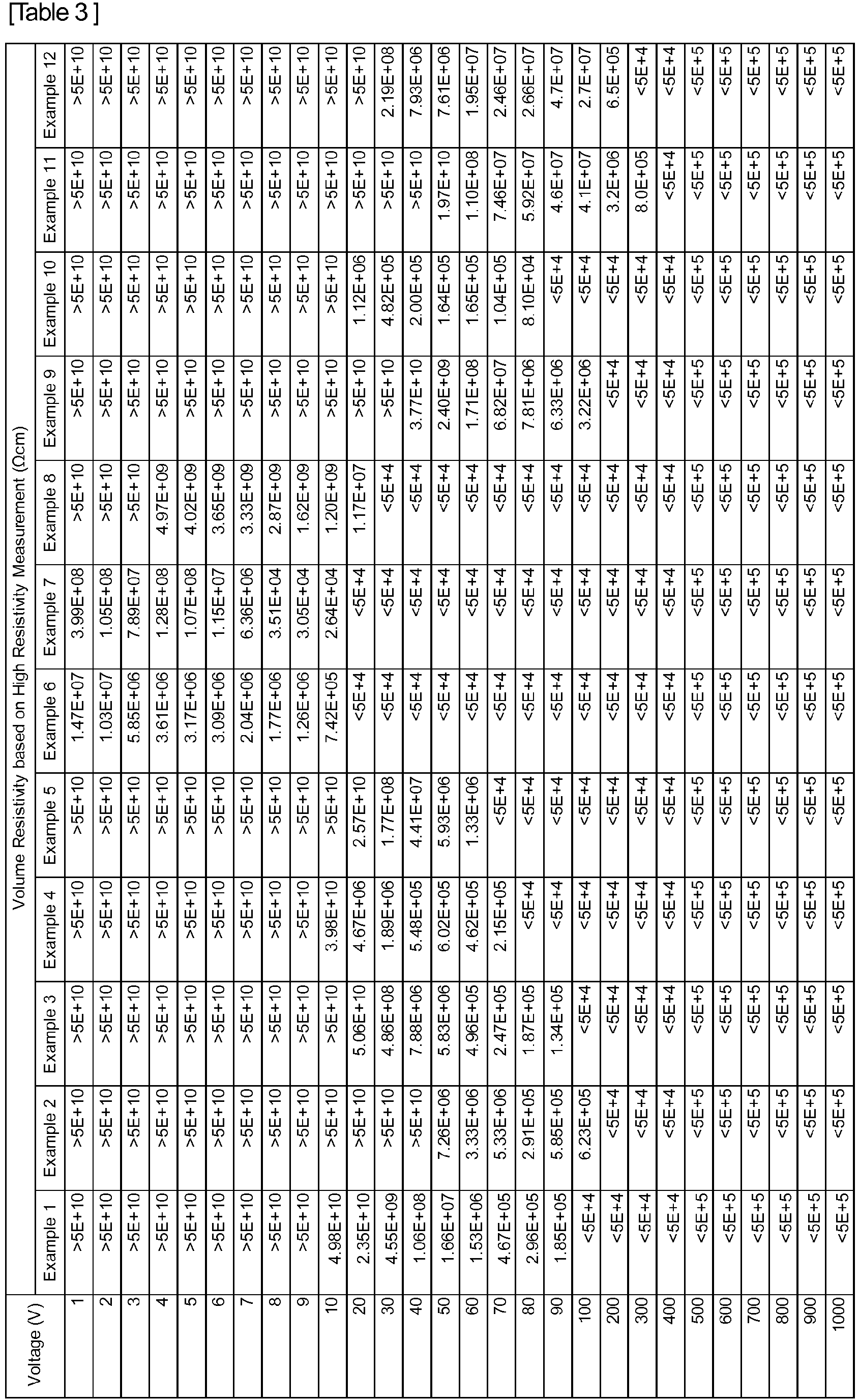

- With the sintered sputtering target of the present invention, the resistance decreases during high voltage application, and DC sputtering is thereby enabled. Accordingly, the present invention yields a superior effect of being able to deposit a transparent film having a low refractive index and high transmissivity even without having to introduce oxygen during film deposition by sputtering. DC sputtering yields significant effects of being able to facilitate the controllability of sputtering, increase the deposition rate, and improve the sputtering efficiency. Moreover, DC sputtering is also able to reduce particles (dust emission) and nodules that are generated during sputter deposition, and improve mass productivity with minimal variation in quality. The thin film formed using the target of the present invention can be used to form optical adjustment films in various displays and protective films of optical disks, and exhibits extremely superior effects in terms of transmissivity and refractive index. Furthermore, a major feature of the present invention is that it is an amorphous film, and the present invention thereby yields a superior effect of preventing cracks in the films and dramatically improving the etching performance of the films.
Claims (14)
- A sintered compact essentially consisting of zinc (Zn), gallium (Ga), silicon (Si) and oxygen (O), wherein a Zn content expressed in terms of ZnO is 5 to 60 mol%, a Ga content expressed in terms of Ga2O3 is 8.5 to 90 mol%, and a Si content expressed in terms of SiO2 is 0 to 45 mol%, and the sintered compact satisfies a condition of A ≤ (B + 2C) when the Zn content expressed in terms of ZnO is A (mol%), the Ga content expressed in terms of Ga2O3 is B (mol%), and the Si content expressed in terms of SiO2 is C (mol%), and has a relative density of 90% or higher.
- The sintered compact according to claim 1, wherein an atomic ratio of Zn and Ga satisfies a condition of Ga/(Ga + Zn) > 0.21.
- The sintered compact according to claim 1 or claim 2, wherein the sintered compact has a diffraction peak attributed to ZnGa2O4 in an X-ray diffraction.
- The sintered compact according to any one of claims 1 to 3, wherein a volume resistivity measured with a constant current application method is 50 kΩ•cm or more.
- The sintered compact according to any one of claims 1 to 4, wherein the relative density is 95% or higher.
- The sintered compact according to any one of claims 1 to 5, wherein a L* value is 65 or more.
- A sputtering target made from the sintered compact according to any one of claims 1 to 6.
- The sputtering target according to claim 7, wherein the volume resistivity measured with the constant voltage application method upon applying a voltage of 1 V is 1 × 10⁶ Ωcm or more.
- The sputtering target according to claim 7 or claim 8, wherein the volume resistivity measured with the constant voltage application method upon applying a voltage of 500 V is 1/100 or less relative to the volume resistivity measured with the constant voltage application method upon applying a voltage of 1 V.
- A thin film essentially consisting of zinc (Zn), gallium (Ga), silicon (Si) and oxygen (O), wherein a Zn content expressed in terms of ZnO is 5 to 60 mol%, a Ga content expressed in terms of Ga2O3 is 8.5 to 90 mol%, and a Si content expressed in terms of SiO2 is 0 to 45 mol%, and the thin film satisfies a condition of A ≤ (B + 2C) when the Zn content expressed in terms of ZnO is A (mol%), the Ga content expressed in terms of Ga2O3 is B (mol%), and the Si content expressed in terms of SiO2 is C (mol%).
- The thin film according to claim 10, wherein a refractive index at a wavelength of 633 nm is 1.95 or less.
- The thin film according to claim 10 or claim 11, wherein an extinction coefficient at a wavelength of 405 nm is 0.05 or less.
- The thin film according to any one of claims 10 to 12, wherein the thin film is amorphous.
- The thin film according to any one of claims 10 to 13, wherein the thin film is produced by being deposited via sputtering in an inert gas atmosphere without oxygen introduction.
Applications Claiming Priority (2)
| Application Number | Priority Date | Filing Date | Title |
|---|---|---|---|
| JP2015038572 | 2015-02-27 | ||
| PCT/JP2016/055554 WO2016136855A1 (en) | 2015-02-27 | 2016-02-25 | Oxide sintered compact, oxide sputtering target, and oxide thin film |
Publications (3)
| Publication Number | Publication Date |
|---|---|
| EP3210952A1 true EP3210952A1 (en) | 2017-08-30 |
| EP3210952A4 EP3210952A4 (en) | 2018-05-23 |
| EP3210952B1 EP3210952B1 (en) | 2019-05-01 |
Family
ID=56789556
Family Applications (1)
| Application Number | Title | Priority Date | Filing Date |
|---|---|---|---|
| EP16755599.4A Active EP3210952B1 (en) | 2015-02-27 | 2016-02-25 | Oxide sintered compact, oxide sputtering target, and oxide thin film |
Country Status (7)
| Country | Link |
|---|---|
| US (1) | US10227261B2 (en) |
| EP (1) | EP3210952B1 (en) |
| JP (1) | JP6023920B1 (en) |
| KR (1) | KR102000856B1 (en) |
| CN (1) | CN107207356B (en) |
| TW (1) | TWI616424B (en) |
| WO (1) | WO2016136855A1 (en) |
Families Citing this family (6)
| Publication number | Priority date | Publication date | Assignee | Title |
|---|---|---|---|---|
| JP6397593B1 (en) * | 2017-10-02 | 2018-09-26 | 住友化学株式会社 | Sputtering target |
| JP6724266B2 (en) | 2018-03-01 | 2020-07-15 | Jx金属株式会社 | Potassium sodium niobate sputtering target and manufacturing method thereof |
| JP7257562B2 (en) * | 2021-04-27 | 2023-04-13 | Jx金属株式会社 | LAMINATED FUNCTION AS TRANSPARENT CONDUCTIVE FILM, METHOD FOR MANUFACTURING SAME, AND OXIDE SPUTTERING TARGET FOR MANUFACTURING SAME LAMINATED PRODUCT |
| US20240183022A1 (en) * | 2021-04-27 | 2024-06-06 | JX Nippon Mining Metals Corporation | Layered body having function as transparent electroconductive film and method for producing same, and oxide sputtering target for said layered body production |
| TWI839845B (en) * | 2021-10-06 | 2024-04-21 | 南韓商Lt金屬股份有限公司 | Molybdenum oxide based sintered body, sputtering target, oxide thin film using the sintered body, and thin film transistors and display devices including the thin films |
| JP7796184B1 (en) * | 2024-08-22 | 2026-01-08 | 株式会社アルバック | Oxide semiconductor thin film, thin film semiconductor device and method for manufacturing the same |
Family Cites Families (31)
| Publication number | Priority date | Publication date | Assignee | Title |
|---|---|---|---|---|
| JPS5339100A (en) | 1976-09-22 | 1978-04-10 | Hitachi Ltd | Driving system of electrochromic display body |
| JPH07111482B2 (en) | 1986-11-21 | 1995-11-29 | 日本板硝子株式会社 | Multi-layer antireflection film |
| JP2566634B2 (en) | 1988-10-04 | 1996-12-25 | キヤノン株式会社 | Multi-layer antireflection film |
| JP2915513B2 (en) | 1990-07-24 | 1999-07-05 | リコー光学株式会社 | Anti-reflective coating |
| JPH0625838A (en) * | 1992-07-10 | 1994-02-01 | Asahi Glass Co Ltd | Sputtering target |
| EP0578046B1 (en) | 1992-07-10 | 1996-11-06 | Asahi Glass Company Ltd. | Transparent conductive film, and target and material for vapor deposition to be used for its production |
| JP3636914B2 (en) | 1998-02-16 | 2005-04-06 | 株式会社日鉱マテリアルズ | High resistance transparent conductive film, method for producing high resistance transparent conductive film, and sputtering target for forming high resistance transparent conductive film |
| JP3841388B2 (en) * | 1998-02-16 | 2006-11-01 | 日鉱金属株式会社 | Protective film for optical disk and sputtering target for forming protective film of optical disk |
| JP3915109B2 (en) * | 1999-09-28 | 2007-05-16 | 三菱マテリアル株式会社 | Sputtering target material for forming an optical recording medium protective layer |
| JP2001115157A (en) * | 1999-10-15 | 2001-04-24 | Nippon Sheet Glass Co Ltd | Phosphor and its production method |
| EP1897968B1 (en) | 2005-06-28 | 2013-08-07 | JX Nippon Mining & Metals Corporation | Gallium oxide-zinc oxide sputtering target, method of forming transparent conductive film and transparent conductive film |
| WO2007000878A1 (en) | 2005-06-28 | 2007-01-04 | Nippon Mining & Metals Co., Ltd. | Gallium oxide-zinc oxide sputtering target, method for forming transparent conductive film, and transparent conductive film |
| WO2007066490A1 (en) | 2005-12-08 | 2007-06-14 | Nippon Mining & Metals Co., Ltd. | Gallium oxide/zinc oxide sputtering target, method of forming transparent conductive film and transparent conductive film |
| US7699965B2 (en) | 2006-03-17 | 2010-04-20 | Nippon Mining & Metals Co., Ltd. | Zinc oxide-based transparent conductor and sputtering target for forming the transparent conductor |
| JP5358891B2 (en) | 2006-08-11 | 2013-12-04 | 日立金属株式会社 | Method for producing sintered zinc oxide |
| JP5090358B2 (en) | 2006-08-24 | 2012-12-05 | Jx日鉱日石金属株式会社 | Zinc oxide-based transparent conductor, sputtering target for forming the transparent conductor, and method for producing the target |
| JP4231967B2 (en) * | 2006-10-06 | 2009-03-04 | 住友金属鉱山株式会社 | Oxide sintered body, method for producing the same, transparent conductive film, and solar cell obtained using the same |
| JP2009256762A (en) * | 2008-04-18 | 2009-11-05 | Toyoshima Seisakusho:Kk | Sputtering target and method for producing the same |
| JP5202630B2 (en) | 2008-06-10 | 2013-06-05 | Jx日鉱日石金属株式会社 | Oxide sintered compact target for sputtering and manufacturing method thereof |
| CN102459122B (en) | 2009-06-05 | 2014-02-05 | 吉坤日矿日石金属株式会社 | Oxide sintered body, method for producing same, and starting material powder for producing oxide sintered body |
| KR20170024124A (en) * | 2011-02-10 | 2017-03-06 | 미쓰비시 마테리알 가부시키가이샤 | Sputtering target for forming transparent film for solar cells, and process for production thereof |
| JP5339100B2 (en) * | 2011-09-22 | 2013-11-13 | 住友金属鉱山株式会社 | Zn-Si-O-based oxide sintered body, method for producing the same, sputtering target, and tablet for vapor deposition |
| JP5954620B2 (en) | 2012-04-04 | 2016-07-20 | 三菱マテリアル株式会社 | Sputtering target for forming transparent oxide film and method for producing the same |
| KR20140006700A (en) * | 2012-06-26 | 2014-01-16 | 삼성코닝정밀소재 주식회사 | Zno based sputtering target, method of fabricating thereof and thin film transistor having shielding layer deposited by the same |
| JP2014005538A (en) * | 2012-06-26 | 2014-01-16 | Samsung Corning Precision Materials Co Ltd | Zinc oxide-based sputtering target, method of manufacturing the same, and thin film transistor having shield film evaporated through the same |
| TWI631579B (en) * | 2012-07-03 | 2018-08-01 | Jx日鑛日石金屬股份有限公司 | Sintered body and amorphous film |
| JP2014009150A (en) | 2012-07-03 | 2014-01-20 | Sumitomo Chemical Co Ltd | Method for producing zinc oxide sintered body |
| JP5550768B1 (en) * | 2012-07-03 | 2014-07-16 | Jx日鉱日石金属株式会社 | Sintered body and amorphous film |
| JP6278229B2 (en) * | 2012-08-10 | 2018-02-14 | 三菱マテリアル株式会社 | Sputtering target for forming transparent oxide film and method for producing the same |
| JP5674747B2 (en) | 2012-11-12 | 2015-02-25 | 株式会社半導体エネルギー研究所 | Semiconductor device |
| KR20140140187A (en) * | 2013-05-28 | 2014-12-09 | 삼성코닝어드밴스드글라스 유한회사 | ZnO BASED SPUTTERING TARGET AND PHOTOVOLTAIC CELL HAVING PASSIVATION LAYER DEPOSITED BY THE SAME |
-
2016
- 2016-02-25 KR KR1020177019389A patent/KR102000856B1/en active Active
- 2016-02-25 WO PCT/JP2016/055554 patent/WO2016136855A1/en not_active Ceased
- 2016-02-25 EP EP16755599.4A patent/EP3210952B1/en active Active
- 2016-02-25 JP JP2016537578A patent/JP6023920B1/en active Active
- 2016-02-25 US US15/542,559 patent/US10227261B2/en active Active
- 2016-02-25 CN CN201680006701.3A patent/CN107207356B/en active Active
- 2016-02-26 TW TW105105783A patent/TWI616424B/en active
Also Published As
| Publication number | Publication date |
|---|---|
| EP3210952A4 (en) | 2018-05-23 |
| KR102000856B1 (en) | 2019-07-16 |
| KR20170094416A (en) | 2017-08-17 |
| CN107207356A (en) | 2017-09-26 |
| CN107207356B (en) | 2020-12-08 |
| EP3210952B1 (en) | 2019-05-01 |
| JP6023920B1 (en) | 2016-11-09 |
| JPWO2016136855A1 (en) | 2017-04-27 |
| TW201702206A (en) | 2017-01-16 |
| US10227261B2 (en) | 2019-03-12 |
| WO2016136855A1 (en) | 2016-09-01 |
| US20180265412A1 (en) | 2018-09-20 |
| TWI616424B (en) | 2018-03-01 |
Similar Documents
| Publication | Publication Date | Title |
|---|---|---|
| EP3210952B1 (en) | Oxide sintered compact, oxide sputtering target, and oxide thin film | |
| TWI525060B (en) | An oxide sintered body, a sputtering target, a thin film, and an oxide sintered body | |
| KR102315765B1 (en) | Oxide thin film, and oxide sintered body for sputtering target for producing oxide thin film | |
| WO2012017659A1 (en) | Method for producing sputtering target, and sputtering target | |
| JP6278229B2 (en) | Sputtering target for forming transparent oxide film and method for producing the same | |
| KR20170084351A (en) | Transparent oxide film and process for producing same | |
| KR101600261B1 (en) | Oxide sintered compact, sputtering target and oxide thin film | |
| KR20150120996A (en) | Niobium oxide sputtering target, production method therefor, and niobium oxide film | |
| JP5876172B1 (en) | Oxide sintered body, oxide sputtering target, conductive oxide thin film, and method for producing oxide sintered body | |
| WO2011010603A1 (en) | TARGET FOR ZnO-BASED TRANSPARENT CONDUCTIVE FILM AND METHOD FOR PRODUCING SAME | |
| WO2014168073A1 (en) | Oxide sputtering target and method for producing same, and protective film for optical recording media | |
| TWI579254B (en) | Sintered and amorphous membranes | |
| KR101945083B1 (en) | Sintered body, sputtering target comprising sintered body and thin film formed by using spattering target | |
| WO2015052927A1 (en) | Sputtering target and method for producing same | |
| JP7726991B2 (en) | Sputtering target and method of manufacturing the same |
Legal Events
| Date | Code | Title | Description |
|---|---|---|---|
| STAA | Information on the status of an ep patent application or granted ep patent |
Free format text: STATUS: THE INTERNATIONAL PUBLICATION HAS BEEN MADE |
|
| PUAI | Public reference made under article 153(3) epc to a published international application that has entered the european phase |
Free format text: ORIGINAL CODE: 0009012 |
|
| STAA | Information on the status of an ep patent application or granted ep patent |
Free format text: STATUS: REQUEST FOR EXAMINATION WAS MADE |
|
| 17P | Request for examination filed |
Effective date: 20170522 |
|
| AK | Designated contracting states |
Kind code of ref document: A1 Designated state(s): AL AT BE BG CH CY CZ DE DK EE ES FI FR GB GR HR HU IE IS IT LI LT LU LV MC MK MT NL NO PL PT RO RS SE SI SK SM TR |
|
| AX | Request for extension of the european patent |
Extension state: BA ME |
|
| RIC1 | Information provided on ipc code assigned before grant |
Ipc: C04B 35/453 20060101AFI20180329BHEP Ipc: C04B 35/00 20060101ALI20180329BHEP Ipc: C23C 14/34 20060101ALI20180329BHEP Ipc: C23C 14/08 20060101ALI20180329BHEP Ipc: H01B 5/14 20060101ALI20180329BHEP |
|
| A4 | Supplementary search report drawn up and despatched |
Effective date: 20180423 |
|
| DAV | Request for validation of the european patent (deleted) | ||
| DAX | Request for extension of the european patent (deleted) | ||
| REG | Reference to a national code |
Ref country code: DE Ref legal event code: R079 Ref document number: 602016013326 Country of ref document: DE Free format text: PREVIOUS MAIN CLASS: C04B0035453000 Ipc: H01B0001080000 |
|
| GRAP | Despatch of communication of intention to grant a patent |
Free format text: ORIGINAL CODE: EPIDOSNIGR1 |
|
| STAA | Information on the status of an ep patent application or granted ep patent |
Free format text: STATUS: GRANT OF PATENT IS INTENDED |
|
| RIC1 | Information provided on ipc code assigned before grant |
Ipc: C04B 35/00 20060101ALI20181205BHEP Ipc: C23C 14/34 20060101ALI20181205BHEP Ipc: H01B 1/08 20060101AFI20181205BHEP Ipc: C23C 14/08 20060101ALI20181205BHEP Ipc: C04B 35/453 20060101ALI20181205BHEP Ipc: H01B 5/14 20060101ALI20181205BHEP |
|
| INTG | Intention to grant announced |
Effective date: 20190103 |
|
| GRAS | Grant fee paid |
Free format text: ORIGINAL CODE: EPIDOSNIGR3 |
|
| GRAA | (expected) grant |
Free format text: ORIGINAL CODE: 0009210 |
|
| STAA | Information on the status of an ep patent application or granted ep patent |
Free format text: STATUS: THE PATENT HAS BEEN GRANTED |
|
| AK | Designated contracting states |
Kind code of ref document: B1 Designated state(s): AL AT BE BG CH CY CZ DE DK EE ES FI FR GB GR HR HU IE IS IT LI LT LU LV MC MK MT NL NO PL PT RO RS SE SI SK SM TR |
|
| REG | Reference to a national code |
Ref country code: GB Ref legal event code: FG4D |
|
| REG | Reference to a national code |
Ref country code: CH Ref legal event code: EP Ref country code: AT Ref legal event code: REF Ref document number: 1128018 Country of ref document: AT Kind code of ref document: T Effective date: 20190515 |
|
| REG | Reference to a national code |
Ref country code: DE Ref legal event code: R096 Ref document number: 602016013326 Country of ref document: DE |
|
| REG | Reference to a national code |
Ref country code: IE Ref legal event code: FG4D |
|
| REG | Reference to a national code |
Ref country code: NL Ref legal event code: MP Effective date: 20190501 |
|
| REG | Reference to a national code |
Ref country code: LT Ref legal event code: MG4D |
|
| PG25 | Lapsed in a contracting state [announced via postgrant information from national office to epo] |
Ref country code: FI Free format text: LAPSE BECAUSE OF FAILURE TO SUBMIT A TRANSLATION OF THE DESCRIPTION OR TO PAY THE FEE WITHIN THE PRESCRIBED TIME-LIMIT Effective date: 20190501 Ref country code: NO Free format text: LAPSE BECAUSE OF FAILURE TO SUBMIT A TRANSLATION OF THE DESCRIPTION OR TO PAY THE FEE WITHIN THE PRESCRIBED TIME-LIMIT Effective date: 20190801 Ref country code: HR Free format text: LAPSE BECAUSE OF FAILURE TO SUBMIT A TRANSLATION OF THE DESCRIPTION OR TO PAY THE FEE WITHIN THE PRESCRIBED TIME-LIMIT Effective date: 20190501 Ref country code: NL Free format text: LAPSE BECAUSE OF FAILURE TO SUBMIT A TRANSLATION OF THE DESCRIPTION OR TO PAY THE FEE WITHIN THE PRESCRIBED TIME-LIMIT Effective date: 20190501 Ref country code: LT Free format text: LAPSE BECAUSE OF FAILURE TO SUBMIT A TRANSLATION OF THE DESCRIPTION OR TO PAY THE FEE WITHIN THE PRESCRIBED TIME-LIMIT Effective date: 20190501 Ref country code: ES Free format text: LAPSE BECAUSE OF FAILURE TO SUBMIT A TRANSLATION OF THE DESCRIPTION OR TO PAY THE FEE WITHIN THE PRESCRIBED TIME-LIMIT Effective date: 20190501 Ref country code: AL Free format text: LAPSE BECAUSE OF FAILURE TO SUBMIT A TRANSLATION OF THE DESCRIPTION OR TO PAY THE FEE WITHIN THE PRESCRIBED TIME-LIMIT Effective date: 20190501 Ref country code: PT Free format text: LAPSE BECAUSE OF FAILURE TO SUBMIT A TRANSLATION OF THE DESCRIPTION OR TO PAY THE FEE WITHIN THE PRESCRIBED TIME-LIMIT Effective date: 20190901 Ref country code: SE Free format text: LAPSE BECAUSE OF FAILURE TO SUBMIT A TRANSLATION OF THE DESCRIPTION OR TO PAY THE FEE WITHIN THE PRESCRIBED TIME-LIMIT Effective date: 20190501 |
|
| PG25 | Lapsed in a contracting state [announced via postgrant information from national office to epo] |
Ref country code: LV Free format text: LAPSE BECAUSE OF FAILURE TO SUBMIT A TRANSLATION OF THE DESCRIPTION OR TO PAY THE FEE WITHIN THE PRESCRIBED TIME-LIMIT Effective date: 20190501 Ref country code: GR Free format text: LAPSE BECAUSE OF FAILURE TO SUBMIT A TRANSLATION OF THE DESCRIPTION OR TO PAY THE FEE WITHIN THE PRESCRIBED TIME-LIMIT Effective date: 20190802 Ref country code: RS Free format text: LAPSE BECAUSE OF FAILURE TO SUBMIT A TRANSLATION OF THE DESCRIPTION OR TO PAY THE FEE WITHIN THE PRESCRIBED TIME-LIMIT Effective date: 20190501 Ref country code: BG Free format text: LAPSE BECAUSE OF FAILURE TO SUBMIT A TRANSLATION OF THE DESCRIPTION OR TO PAY THE FEE WITHIN THE PRESCRIBED TIME-LIMIT Effective date: 20190801 |
|
| REG | Reference to a national code |
Ref country code: AT Ref legal event code: MK05 Ref document number: 1128018 Country of ref document: AT Kind code of ref document: T Effective date: 20190501 |
|
| PG25 | Lapsed in a contracting state [announced via postgrant information from national office to epo] |
Ref country code: IS Free format text: LAPSE BECAUSE OF FAILURE TO SUBMIT A TRANSLATION OF THE DESCRIPTION OR TO PAY THE FEE WITHIN THE PRESCRIBED TIME-LIMIT Effective date: 20190901 |
|
| PG25 | Lapsed in a contracting state [announced via postgrant information from national office to epo] |
Ref country code: SK Free format text: LAPSE BECAUSE OF FAILURE TO SUBMIT A TRANSLATION OF THE DESCRIPTION OR TO PAY THE FEE WITHIN THE PRESCRIBED TIME-LIMIT Effective date: 20190501 Ref country code: CZ Free format text: LAPSE BECAUSE OF FAILURE TO SUBMIT A TRANSLATION OF THE DESCRIPTION OR TO PAY THE FEE WITHIN THE PRESCRIBED TIME-LIMIT Effective date: 20190501 Ref country code: RO Free format text: LAPSE BECAUSE OF FAILURE TO SUBMIT A TRANSLATION OF THE DESCRIPTION OR TO PAY THE FEE WITHIN THE PRESCRIBED TIME-LIMIT Effective date: 20190501 Ref country code: EE Free format text: LAPSE BECAUSE OF FAILURE TO SUBMIT A TRANSLATION OF THE DESCRIPTION OR TO PAY THE FEE WITHIN THE PRESCRIBED TIME-LIMIT Effective date: 20190501 Ref country code: DK Free format text: LAPSE BECAUSE OF FAILURE TO SUBMIT A TRANSLATION OF THE DESCRIPTION OR TO PAY THE FEE WITHIN THE PRESCRIBED TIME-LIMIT Effective date: 20190501 Ref country code: AT Free format text: LAPSE BECAUSE OF FAILURE TO SUBMIT A TRANSLATION OF THE DESCRIPTION OR TO PAY THE FEE WITHIN THE PRESCRIBED TIME-LIMIT Effective date: 20190501 |
|
| REG | Reference to a national code |
Ref country code: DE Ref legal event code: R097 Ref document number: 602016013326 Country of ref document: DE |
|
| PG25 | Lapsed in a contracting state [announced via postgrant information from national office to epo] |
Ref country code: IT Free format text: LAPSE BECAUSE OF FAILURE TO SUBMIT A TRANSLATION OF THE DESCRIPTION OR TO PAY THE FEE WITHIN THE PRESCRIBED TIME-LIMIT Effective date: 20190501 Ref country code: SM Free format text: LAPSE BECAUSE OF FAILURE TO SUBMIT A TRANSLATION OF THE DESCRIPTION OR TO PAY THE FEE WITHIN THE PRESCRIBED TIME-LIMIT Effective date: 20190501 |
|
| PLBE | No opposition filed within time limit |
Free format text: ORIGINAL CODE: 0009261 |
|
| STAA | Information on the status of an ep patent application or granted ep patent |
Free format text: STATUS: NO OPPOSITION FILED WITHIN TIME LIMIT |
|
| PG25 | Lapsed in a contracting state [announced via postgrant information from national office to epo] |
Ref country code: TR Free format text: LAPSE BECAUSE OF FAILURE TO SUBMIT A TRANSLATION OF THE DESCRIPTION OR TO PAY THE FEE WITHIN THE PRESCRIBED TIME-LIMIT Effective date: 20190501 |
|
| 26N | No opposition filed |
Effective date: 20200204 |
|
| PG25 | Lapsed in a contracting state [announced via postgrant information from national office to epo] |
Ref country code: PL Free format text: LAPSE BECAUSE OF FAILURE TO SUBMIT A TRANSLATION OF THE DESCRIPTION OR TO PAY THE FEE WITHIN THE PRESCRIBED TIME-LIMIT Effective date: 20190501 |
|
| PG25 | Lapsed in a contracting state [announced via postgrant information from national office to epo] |
Ref country code: SI Free format text: LAPSE BECAUSE OF FAILURE TO SUBMIT A TRANSLATION OF THE DESCRIPTION OR TO PAY THE FEE WITHIN THE PRESCRIBED TIME-LIMIT Effective date: 20190501 |
|
| REG | Reference to a national code |
Ref country code: CH Ref legal event code: PL |
|
| GBPC | Gb: european patent ceased through non-payment of renewal fee |
Effective date: 20200225 |
|
| REG | Reference to a national code |
Ref country code: BE Ref legal event code: MM Effective date: 20200229 |
|
| PG25 | Lapsed in a contracting state [announced via postgrant information from national office to epo] |
Ref country code: MC Free format text: LAPSE BECAUSE OF FAILURE TO SUBMIT A TRANSLATION OF THE DESCRIPTION OR TO PAY THE FEE WITHIN THE PRESCRIBED TIME-LIMIT Effective date: 20190501 Ref country code: LU Free format text: LAPSE BECAUSE OF NON-PAYMENT OF DUE FEES Effective date: 20200225 |
|
| PG25 | Lapsed in a contracting state [announced via postgrant information from national office to epo] |
Ref country code: CH Free format text: LAPSE BECAUSE OF NON-PAYMENT OF DUE FEES Effective date: 20200229 Ref country code: LI Free format text: LAPSE BECAUSE OF NON-PAYMENT OF DUE FEES Effective date: 20200229 |
|
| PG25 | Lapsed in a contracting state [announced via postgrant information from national office to epo] |
Ref country code: IE Free format text: LAPSE BECAUSE OF NON-PAYMENT OF DUE FEES Effective date: 20200225 Ref country code: GB Free format text: LAPSE BECAUSE OF NON-PAYMENT OF DUE FEES Effective date: 20200225 |
|
| PG25 | Lapsed in a contracting state [announced via postgrant information from national office to epo] |
Ref country code: BE Free format text: LAPSE BECAUSE OF NON-PAYMENT OF DUE FEES Effective date: 20200229 |
|
| PG25 | Lapsed in a contracting state [announced via postgrant information from national office to epo] |
Ref country code: MT Free format text: LAPSE BECAUSE OF FAILURE TO SUBMIT A TRANSLATION OF THE DESCRIPTION OR TO PAY THE FEE WITHIN THE PRESCRIBED TIME-LIMIT Effective date: 20190501 Ref country code: CY Free format text: LAPSE BECAUSE OF FAILURE TO SUBMIT A TRANSLATION OF THE DESCRIPTION OR TO PAY THE FEE WITHIN THE PRESCRIBED TIME-LIMIT Effective date: 20190501 |
|
| PG25 | Lapsed in a contracting state [announced via postgrant information from national office to epo] |
Ref country code: MK Free format text: LAPSE BECAUSE OF FAILURE TO SUBMIT A TRANSLATION OF THE DESCRIPTION OR TO PAY THE FEE WITHIN THE PRESCRIBED TIME-LIMIT Effective date: 20190501 |
|
| P01 | Opt-out of the competence of the unified patent court (upc) registered |
Effective date: 20230517 |
|
| PGFP | Annual fee paid to national office [announced via postgrant information from national office to epo] |
Ref country code: FR Payment date: 20251231 Year of fee payment: 11 |
|
| PGFP | Annual fee paid to national office [announced via postgrant information from national office to epo] |
Ref country code: DE Payment date: 20260102 Year of fee payment: 11 |