EP3208896A1 - Semiconductor laser device - Google Patents
Semiconductor laser device Download PDFInfo
- Publication number
- EP3208896A1 EP3208896A1 EP15851412.5A EP15851412A EP3208896A1 EP 3208896 A1 EP3208896 A1 EP 3208896A1 EP 15851412 A EP15851412 A EP 15851412A EP 3208896 A1 EP3208896 A1 EP 3208896A1
- Authority
- EP
- European Patent Office
- Prior art keywords
- semiconductor laser
- stem
- laser device
- power
- external terminal
- Prior art date
- Legal status (The legal status is an assumption and is not a legal conclusion. Google has not performed a legal analysis and makes no representation as to the accuracy of the status listed.)
- Withdrawn
Links
Images



Classifications
-
- H—ELECTRICITY
- H01—ELECTRIC ELEMENTS
- H01S—DEVICES USING THE PROCESS OF LIGHT AMPLIFICATION BY STIMULATED EMISSION OF RADIATION [LASER] TO AMPLIFY OR GENERATE LIGHT; DEVICES USING STIMULATED EMISSION OF ELECTROMAGNETIC RADIATION IN WAVE RANGES OTHER THAN OPTICAL
- H01S5/00—Semiconductor lasers
- H01S5/02—Structural details or components not essential to laser action
- H01S5/024—Arrangements for thermal management
- H01S5/02476—Heat spreaders, i.e. improving heat flow between laser chip and heat dissipating elements
-
- H—ELECTRICITY
- H01—ELECTRIC ELEMENTS
- H01S—DEVICES USING THE PROCESS OF LIGHT AMPLIFICATION BY STIMULATED EMISSION OF RADIATION [LASER] TO AMPLIFY OR GENERATE LIGHT; DEVICES USING STIMULATED EMISSION OF ELECTROMAGNETIC RADIATION IN WAVE RANGES OTHER THAN OPTICAL
- H01S5/00—Semiconductor lasers
- H01S5/005—Optical components external to the laser cavity, specially adapted therefor, e.g. for homogenisation or merging of the beams or for manipulating laser pulses, e.g. pulse shaping
- H01S5/0087—Optical components external to the laser cavity, specially adapted therefor, e.g. for homogenisation or merging of the beams or for manipulating laser pulses, e.g. pulse shaping for illuminating phosphorescent or fluorescent materials, e.g. using optical arrangements specifically adapted for guiding or shaping laser beams illuminating these materials
-
- H—ELECTRICITY
- H01—ELECTRIC ELEMENTS
- H01S—DEVICES USING THE PROCESS OF LIGHT AMPLIFICATION BY STIMULATED EMISSION OF RADIATION [LASER] TO AMPLIFY OR GENERATE LIGHT; DEVICES USING STIMULATED EMISSION OF ELECTROMAGNETIC RADIATION IN WAVE RANGES OTHER THAN OPTICAL
- H01S5/00—Semiconductor lasers
- H01S5/02—Structural details or components not essential to laser action
- H01S5/022—Mountings; Housings
- H01S5/02208—Mountings; Housings characterised by the shape of the housings
- H01S5/02212—Can-type, e.g. TO-CAN housings with emission along or parallel to symmetry axis
-
- H—ELECTRICITY
- H01—ELECTRIC ELEMENTS
- H01S—DEVICES USING THE PROCESS OF LIGHT AMPLIFICATION BY STIMULATED EMISSION OF RADIATION [LASER] TO AMPLIFY OR GENERATE LIGHT; DEVICES USING STIMULATED EMISSION OF ELECTROMAGNETIC RADIATION IN WAVE RANGES OTHER THAN OPTICAL
- H01S5/00—Semiconductor lasers
- H01S5/02—Structural details or components not essential to laser action
- H01S5/022—Mountings; Housings
- H01S5/0225—Out-coupling of light
- H01S5/02257—Out-coupling of light using windows, e.g. specially adapted for back-reflecting light to a detector inside the housing
-
- H—ELECTRICITY
- H01—ELECTRIC ELEMENTS
- H01S—DEVICES USING THE PROCESS OF LIGHT AMPLIFICATION BY STIMULATED EMISSION OF RADIATION [LASER] TO AMPLIFY OR GENERATE LIGHT; DEVICES USING STIMULATED EMISSION OF ELECTROMAGNETIC RADIATION IN WAVE RANGES OTHER THAN OPTICAL
- H01S5/00—Semiconductor lasers
- H01S5/02—Structural details or components not essential to laser action
- H01S5/022—Mountings; Housings
- H01S5/023—Mount members, e.g. sub-mount members
-
- H—ELECTRICITY
- H01—ELECTRIC ELEMENTS
- H01S—DEVICES USING THE PROCESS OF LIGHT AMPLIFICATION BY STIMULATED EMISSION OF RADIATION [LASER] TO AMPLIFY OR GENERATE LIGHT; DEVICES USING STIMULATED EMISSION OF ELECTROMAGNETIC RADIATION IN WAVE RANGES OTHER THAN OPTICAL
- H01S5/00—Semiconductor lasers
- H01S5/02—Structural details or components not essential to laser action
- H01S5/022—Mountings; Housings
- H01S5/023—Mount members, e.g. sub-mount members
- H01S5/0231—Stems
-
- H—ELECTRICITY
- H01—ELECTRIC ELEMENTS
- H01S—DEVICES USING THE PROCESS OF LIGHT AMPLIFICATION BY STIMULATED EMISSION OF RADIATION [LASER] TO AMPLIFY OR GENERATE LIGHT; DEVICES USING STIMULATED EMISSION OF ELECTROMAGNETIC RADIATION IN WAVE RANGES OTHER THAN OPTICAL
- H01S5/00—Semiconductor lasers
- H01S5/02—Structural details or components not essential to laser action
- H01S5/022—Mountings; Housings
- H01S5/0233—Mounting configuration of laser chips
-
- H—ELECTRICITY
- H01—ELECTRIC ELEMENTS
- H01S—DEVICES USING THE PROCESS OF LIGHT AMPLIFICATION BY STIMULATED EMISSION OF RADIATION [LASER] TO AMPLIFY OR GENERATE LIGHT; DEVICES USING STIMULATED EMISSION OF ELECTROMAGNETIC RADIATION IN WAVE RANGES OTHER THAN OPTICAL
- H01S5/00—Semiconductor lasers
- H01S5/02—Structural details or components not essential to laser action
- H01S5/022—Mountings; Housings
- H01S5/0235—Method for mounting laser chips
-
- H—ELECTRICITY
- H01—ELECTRIC ELEMENTS
- H01S—DEVICES USING THE PROCESS OF LIGHT AMPLIFICATION BY STIMULATED EMISSION OF RADIATION [LASER] TO AMPLIFY OR GENERATE LIGHT; DEVICES USING STIMULATED EMISSION OF ELECTROMAGNETIC RADIATION IN WAVE RANGES OTHER THAN OPTICAL
- H01S5/00—Semiconductor lasers
- H01S5/02—Structural details or components not essential to laser action
- H01S5/022—Mountings; Housings
- H01S5/0239—Combinations of electrical or optical elements
-
- H—ELECTRICITY
- H01—ELECTRIC ELEMENTS
- H01S—DEVICES USING THE PROCESS OF LIGHT AMPLIFICATION BY STIMULATED EMISSION OF RADIATION [LASER] TO AMPLIFY OR GENERATE LIGHT; DEVICES USING STIMULATED EMISSION OF ELECTROMAGNETIC RADIATION IN WAVE RANGES OTHER THAN OPTICAL
- H01S5/00—Semiconductor lasers
- H01S5/02—Structural details or components not essential to laser action
- H01S5/024—Arrangements for thermal management
-
- H—ELECTRICITY
- H01—ELECTRIC ELEMENTS
- H01S—DEVICES USING THE PROCESS OF LIGHT AMPLIFICATION BY STIMULATED EMISSION OF RADIATION [LASER] TO AMPLIFY OR GENERATE LIGHT; DEVICES USING STIMULATED EMISSION OF ELECTROMAGNETIC RADIATION IN WAVE RANGES OTHER THAN OPTICAL
- H01S5/00—Semiconductor lasers
- H01S5/02—Structural details or components not essential to laser action
- H01S5/024—Arrangements for thermal management
- H01S5/02469—Passive cooling, e.g. where heat is removed by the housing as a whole or by a heat pipe without any active cooling element like a TEC
-
- H—ELECTRICITY
- H10—SEMICONDUCTOR DEVICES; ELECTRIC SOLID-STATE DEVICES NOT OTHERWISE PROVIDED FOR
- H10W—GENERIC PACKAGES, INTERCONNECTIONS, CONNECTORS OR OTHER CONSTRUCTIONAL DETAILS OF DEVICES COVERED BY CLASS H10
- H10W40/00—Arrangements for thermal protection or thermal control
- H10W40/20—Arrangements for cooling
- H10W40/22—Arrangements for cooling characterised by their shape, e.g. having conical or cylindrical projections
- H10W40/226—Arrangements for cooling characterised by their shape, e.g. having conical or cylindrical projections characterised by projecting parts, e.g. fins to increase surface area
- H10W40/228—Arrangements for cooling characterised by their shape, e.g. having conical or cylindrical projections characterised by projecting parts, e.g. fins to increase surface area the projecting parts being wire-shaped or pin-shaped
-
- H—ELECTRICITY
- H10—SEMICONDUCTOR DEVICES; ELECTRIC SOLID-STATE DEVICES NOT OTHERWISE PROVIDED FOR
- H10W—GENERIC PACKAGES, INTERCONNECTIONS, CONNECTORS OR OTHER CONSTRUCTIONAL DETAILS OF DEVICES COVERED BY CLASS H10
- H10W76/00—Containers; Fillings or auxiliary members therefor; Seals
- H10W76/10—Containers or parts thereof
- H10W76/12—Containers or parts thereof characterised by their shape
- H10W76/13—Containers comprising a conductive base serving as an interconnection
- H10W76/132—Containers comprising a conductive base serving as an interconnection having other interconnections through an insulated passage in the conductive base
-
- H—ELECTRICITY
- H01—ELECTRIC ELEMENTS
- H01S—DEVICES USING THE PROCESS OF LIGHT AMPLIFICATION BY STIMULATED EMISSION OF RADIATION [LASER] TO AMPLIFY OR GENERATE LIGHT; DEVICES USING STIMULATED EMISSION OF ELECTROMAGNETIC RADIATION IN WAVE RANGES OTHER THAN OPTICAL
- H01S5/00—Semiconductor lasers
- H01S5/02—Structural details or components not essential to laser action
- H01S5/022—Mountings; Housings
- H01S5/0233—Mounting configuration of laser chips
- H01S5/02345—Wire-bonding
Definitions
- the present invention relates to a semiconductor laser device.
- Patent Document 1 A semiconductor laser device in which a semiconductor laser element is fixed to a stem and covered with a cap is known in Patent Document 1 or the like. Such a semiconductor laser device is mounted and used in a mounting object such as an image display device, a lighting fixture or a vehicle lamp.
- the semiconductor laser device disclosed in the Patent Document 1 emits laser light upward through a translucent member provided on an upper surface of the cap.
- Patent Document 1 Japanese Patent Publication No. 5347231
- the semiconductor laser device disclosed in the Patent Document 1 has room for improvement in heat dissipation properties.
- a semiconductor laser device is mounted on a mounting object.
- the semiconductor laser device includes a stem; a cap that has a translucent member and is attached to an upper surface of the stem to form an accommodation space between the cap and the stem; a semiconductor laser element that is disposed in the accommodation space and emits laser light; and a power-feeding member that is at least partially buried in the stem and is electrically conducted with the semiconductor laser element, in which the power-feeding member has an element-side terminal that is exposed to the accommodation space and is electrically connected to the semiconductor laser element, and an external terminal connected to an external power source, and in which the external terminal of the power-feeding member is exposed on a side surface or an upper surface of the stem, and an attaching surface to be attached to the mounting object is provided on a lower surface of the stem.
- the external terminal is exposed on the side surface or upper surface of the stem, and thus, it is possible to secure a large attaching surface on the lower surface of the stem. Since it is easy to efficiently transfer the heat, which is transferred from the semiconductor laser element to the stem, to the mounting object via the attaching surface, it is possible to provide the semiconductor laser device with enhanced heat dissipation properties.
- a recessed portion may be provided on the side surface of the stem, and the external terminal may be exposed to the recessed portion.
- the external terminal is provided at a position retracted from an outer surface, and thus, the breakage of the external terminal can be suppressed.
- a plurality of the power-feeding members may be provided, and the external terminal of at least one thereof may be exposed on the side surface of the stem at a position different from the other external terminals, as seen from above.
- the semiconductor laser device having the above configuration, it is easy to arrange the power-feeding members so as to be spaced apart from each other, as seen from above, and heat is less likely to concentrate on a specific area. Thus, it is easy to enhance the heat dissipation properties.
- the semiconductor laser element may be provided on a heat sink fixed to the upper surface of the stem, and an auxiliary conductor having one end connected to the heat sink and the other end exposed on the side surface of the stem may be buried in the stem.
- the heat generated in the semiconductor laser element and transferred to the heat sink is transferred to the stem via the auxiliary conductor, so that the heat can be efficiently transferred from the attaching surface of the stem to the mounting object.
- a positioning portion for positioning the stem on the mounting object may be provided in at least one of the side surface and the lower surface of the stem.
- the semiconductor laser device having the above configuration, it is easy to align the semiconductor laser device at the time of being attached to the mounting object.
- the external terminal may be located in the positioning portion. According to the semiconductor laser device having the above configuration, an operation of connecting the external terminal to the external power source can be accurately performed by using the portion which is easy to align.
- the power-feeding member may have a heat dissipation portion extending along the attaching surface of the stem.
- the heat generated from the semiconductor laser element and transferred to the power-feeding member can be efficiently transferred to the attaching surface via the heat dissipation portion.
- a portion of the power-feeding member buried in the stem and the external terminal may extend in the same linear shape. According to the semiconductor laser device having the above configuration, it is easy to manufacture the power-feeding member.
- the semiconductor laser device with enhanced heat dissipation properties.
- Fig. 1 is a perspective view of a semiconductor laser device 10 according to the first embodiment of the present invention.
- Fig. 2 is a sectional view taken along a line II-II in Fig. 1 .
- the semiconductor laser device 10 includes a stem 11, a cap 12, a semiconductor laser element 13, and a power-feeding member 14.
- the semiconductor laser device 10 is mounted and used in a mounting object T such as, for example, an image display device, a lighting fixture or a vehicle lamp.
- the cap 12 is attached to an upper surface of the stem 11.
- the cap 12 has a disc-shaped upper surface portion 15 and a cylindrical peripheral wall portion 16 extending downward from a peripheral edge of the upper surface portion 15.
- the cap 12 is attached to the upper surface of the stem 11 to form an accommodation space S (see Fig. 2 ) between the cap 12 and the stem 11.
- the cap 12 has a translucent member 17 at a center portion of the upper surface portion 15.
- the translucent member 17 is formed of a material having translucency. In the present embodiment, the translucent member 17 contains a phosphor. Meanwhile, the translucent member 17 may be provided on a side surface portion or the like of the cap 12 other than the upper surface portion 15.
- a direction in which the semiconductor laser element 13 is provided with respect to the stem 11 is referred to as an upper direction
- a direction in which the stem 11 is provided with respect to the semiconductor laser element 13 is referred to as a lower direction
- a direction orthogonal to the upper and lower direction is referred to as a lateral direction.
- the stem 11 includes a mounting portion 21 having a circular shape in a plan view and a positioning portion 22 protruding sideways from a part of the periphery of the mounting portion 21 and having a rectangular shape in a plan view.
- the positioning portion 22 is used for positioning the semiconductor laser device 10 with respect to the mounting object T when the semiconductor laser device 10 is attached to the mounting object T.
- the positioning portion 22 is formed in a shape to be fitted into a recessed portion or the like formed in the mounting object T.
- an upper surface of the circular mounting portion 21 is a mounting surface 11a.
- a lower surface of the mounting portion 21 and a lower surface of the positioning portion 22 are provided as an attaching surface 11b.
- the mounting surface 11a and the attaching surface 11b are formed as a flat surface, respectively.
- the cap 12, the semiconductor laser element 13, a sub-mount 25 and a heat sink 26 are mounted on the mounting surface 11a of the stem 11.
- the semiconductor laser element 13 is a semiconductor element that emits laser light when power is supplied.
- the semiconductor laser element 13 is provided in the accommodation space S so as to irradiate laser light toward the translucent member 17.
- the semiconductor laser element 13 emits blue light.
- the blue light causes the phosphor contained in the translucent member 17 to emit yellow light.
- the semiconductor laser device 10 mixes the blue light and the yellow light and emits white light to the outside.
- the semiconductor laser element 13 is fixed to the sub-mount 25.
- the sub-mount 25 is attached to the heat sink 26 fixed to the mounting surface 11a of the stem 11. In this way, the semiconductor laser element 13 is mounted on the mounting surface 11a of the stem 11 via the sub-mount 25 and the heat sink 26.
- the semiconductor laser device 10 includes a plurality of (in this example, two) power-feeding members 14.
- Each power-feeding member 14 is a member made of a conductive metal. Both ends of each power-feeding member 14 are formed as an element-side end portion 32 and an external terminal 33, respectively.
- An intermediate portion of each power-feeding member 14 is buried in the stem 11.
- An outer periphery of the portion of each power-feeding member 14 buried in the stem 11 is covered with an insulator 31 that is made of an insulating resin.
- Each power-feeding member 14 is bent at a substantially right angle in the intermediate portion thereof. The element-side terminal 32 and the external terminal 33 of each power-feeding member 14 are exposed from the insulator 31.
- each power-feeding member 14 protrudes from the mounting surface 11a of the stem 11 and is exposed to the accommodation space S.
- Each element-side terminal 32 is disposed in the vicinity of the heat sink 26 on which the semiconductor laser element 13 is supported.
- Each element-side terminal 32 is electrically connected to the semiconductor laser element 13 by a bonding wire 35.
- each power-feeding member 14 is exposed on the side surface of the stem 11. Specifically, a recessed portion 23 opened toward the side is provided on the side surface of the positioning portion 22 of the stem 11. Each external terminal 33 is exposed to the recessed portion 23.
- the external terminal 33 of each power-feeding member 14 exposed to the recessed portion 23 is connected to an external power source (not shown). In this way, power can be supplied from the external power source to the semiconductor laser element 13 via the power-feeding members 14.
- Each external terminal 33 extends in the same linear shape as the portion of each power-feeding member 14 buried in the stem 11.
- Fig. 3 is a view showing a structure of the stem 11.
- Fig. 3(a) is a sectional view taken along a line III-III in Fig. 2
- Fig. 3(b) is a sectional view taken along a line b-b in Fig. 3(a) .
- the plurality of power-feeding members 14 are arranged at intervals so as not to overlap with each other, as seen from above. Further, the external terminals 33 of the power-feeding members 14 are exposed to the single recessed portion 23 provided on the side surface of the stem 11.
- the external terminals 33 are provided at positions retracted from the outer surface, the breakage of the external terminals 33 can be suppressed. Further, since the plurality of external terminals 33 are intensively provided in the single recessed portion 23, it is easy to reduce the size of the semiconductor laser device 10 and it is also easy to connect the external terminals 33 and the external power source.
- the external terminals 33 are positioned in the positioning portion 22, it is easy to accurately perform an operation of connecting the external terminals 33 to the external power source by using the positioning portion 22 which is easy to align.
- the semiconductor laser device 10 includes an auxiliary conductor 41.
- the auxiliary conductor 41 is a metal member having better thermal conductivity than resin.
- the auxiliary conductor 41 electrically connects the semiconductor laser element 13 and an external ground terminal.
- One end of the auxiliary conductor 41 is connected to the heat sink 26 and the other end 41b thereof is exposed on the side surface of the stem 11.
- the other end 41b of the auxiliary conductor 41 is exposed to the recessed portion 23 formed in the positioning portion 22.
- the auxiliary conductor 41 is arranged between two power-feeding members 14 and in parallel with the power-feeding members 14.
- An intermediate portion of the auxiliary conductor 41 is bent at a substantially right angle.
- the intermediate portion of the auxiliary conductor 41 is buried in the stem 11.
- An outer periphery of the portion of the auxiliary conductor 41 buried in the stem 11 is covered with an insulator 42 that is made of an insulating resin.
- the semiconductor laser device 10 when power is supplied from the external power source, the power is supplied to the semiconductor laser element 13 through the power-feeding members 14. Then, blue laser light is irradiated upward from the semiconductor laser element 13 and is incident on the translucent member 17. Then, yellow light is emitted from the phosphor contained in the translucent member 17. The blue light and the yellow light are mixed, and thus, white light is emitted to the outside.
- the semiconductor laser element 13 When laser light is emitted from the semiconductor laser element 13 in this way, the semiconductor laser element 13 generates heat. In the semiconductor laser device 10, it is required to promptly discharge the heat generated in the semiconductor laser element 13 in order to maintain good light-emission performance of the semiconductor laser element 13. According to the semiconductor laser device 10 of the present embodiment, the heat of the semiconductor laser element 13 is transferred to the mounting object T via the sub-mount 25, the heat sink 26 and the stem 11, so that the semiconductor laser element 13 is cooled.
- the semiconductor laser device disclosed in the Patent Document 1 is mounted on a mounting object such as, for example, a display device, a lighting fixture or a vehicle lamp
- a lower surface of the stem is fixed to the mounting object.
- an external terminal is exposed on the lower surface of the stem of the semiconductor laser device disclosed in the Patent Document 1. Therefore, it is necessary to secure an area for exposing the external terminal on the lower surface of the stem, and hence, an area on the lower surface of the stem, which can be used as the attaching surface, is limited. Therefore, it is difficult to efficiently transfer the heat, which is generated in the semiconductor laser element and transferred to the stem, to the mounting object via the attaching surface.
- the semiconductor laser device disclosed in the Patent Document 1 has room for improvement in heat dissipation properties.
- the external terminal 33 of each power-feeding member 14 is exposed on the side surface of the stem 11. Therefore, it is possible to secure the large attaching surface 11b on the lower surface of the stem 11, and hence, it is easy to efficiently transfer the heat, which is transferred from the semiconductor laser element 13 to the stem 11, to the mounting object T via the attaching surface 11b. In this way, it is possible to provide the semiconductor laser device 10 with enhanced heat dissipation properties.
- the heat generated in the semiconductor laser element 13 can be efficiently transferred to the stem 11 via the power-feeding members 14 that are made of metal having higher thermal conductivity than resin. Furthermore, the plurality of power-feeding members 14 are arranged so as not to overlap with each other, as seen from above. Therefore, the heat, which is transferred from the semiconductor laser element 13 to the stem 11, is more likely to be uniformly transferred to the stem 11, as seen from above, and hence, the heat is less likely to concentrate only on a specific area of the lower surface of the stem 11. In this way, it is possible to efficiently transfer the heat from the attaching surface 11b of the stem 11 to the mounting object T.
- each power-feeding member 14 buried in the stem 11 extends along the attaching surface 11b of the stem 11 and also serves as a heat dissipation portion 14a.
- the power-feeding members 14 allow the heat generated in the semiconductor laser element 13 to be efficiently transferred to the portion close to the attaching surface 11b of the stem 11, so that the heat can be efficiently dissipated from the attaching surface 11 b of the stem 11 to the mounting object T.
- the semiconductor laser device 10 includes the auxiliary conductor 41.
- the heat generated in the semiconductor laser element 13 is efficiently transferred to the stem 11 via the auxiliary conductor 41, in addition to the power-feeding members 14. Therefore, heat can be efficiently dissipated from the attaching surface 11b of the stem 11 to the mounting object T.
- the attaching surface 11b of the stem 11 is formed as a flat surface, the attaching surface 11b is easily brought into close contact with the mounting surface T, and hence, it is easy to enhance the heat dissipation properties. Meanwhile, when the mounted surface of the mounting object T is a curved surface or a stepped surface, it is preferable that the attaching surface 11b of the stem 11 also has a shape matching the shape of the mounted surface.
- semiconductor laser devices 10A to 10C according to second to fourth embodiments whose configurations are partially different from those of the semiconductor laser device 10 according to the first embodiment will be described. Meanwhile, the same components as those of the first embodiment are denoted by the same reference numerals and description thereof is omitted.
- the power-feeding members 14 are arranged so as not to overlap with each other, as seen from above.
- the present invention is not limited thereto.
- Fig. 4 is a sectional view corresponding to Fig. 2 , showing the semiconductor laser device 10A according to the second embodiment of the present invention.
- the semiconductor laser device 10A is configured such that the portions of the plurality of power-feeding members 14 buried in the stem 11 are arranged in a thickness direction of the stem 11. In this way, the external terminals 33 exposed to the recessed portion 23 are arranged above and below in the recessed portion 23. According to this configuration, a width dimension of the positioning portion 22 of the stem 11 becomes small as seen from above, thereby easily reducing the whole size thereof.
- Fig. 5 is a sectional view corresponding to Fig. 3(a) , showing the semiconductor laser device 10B according to the third embodiment of the present invention.
- Fig. 6 is a sectional view taken along a line XI-XI in Fig. 5 .
- the semiconductor laser device 10B is configured such that two positioning portions 22 are provided in a stem 11B. These positioning portions 22 are provided at positions opposite to each other, as seen from above. Each positioning portion 22 is provided with the recessed portion 23. The portions of the plurality of power-feeding members 14 buried in the stem 11B extend in opposite directions, and hence, each external terminal 33 is exposed to the recessed portion 23 of each positioning portion 22.
- the external terminal 33 of at least one of the plurality of power-feeding members 14 is exposed on the side surface of the stem 11B at a position different from the other external terminals 33, as seen from above.
- the external terminal 33 of at least one of the plurality of power-feeding members 14 is exposed on the side surface of the stem 11B at a position different from the other external terminals 33, as seen from above. Therefore, it is easy to arrange the power-feeding members 14 so as to be spaced apart from each other, as seen from above, and heat is less likely to concentrate on a specific area. Thus, it is easy to enhance the heat dissipation properties. Further, by providing two positioning portions 22, the semiconductor laser device can be more reliably positioned with respect to the mounting object T.
- the auxiliary conductor 41 is not provided.
- the auxiliary conductor 41 may be provided.
- a terminal of the auxiliary conductor 41 exposed to the outside may be exposed on the side surface of the stem 11B at the same position as the portion to which the external terminal 33 of the power-feeding member 14 is exposed, or may be exposed on the side surface of the stem 11B at a position different from the external terminal 33, as seen from above.
- each power-feeding member 14 has a shape bent at a right angle.
- the present invention is not limited thereto.
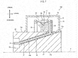
- Fig. 7 is a sectional view corresponding to Fig. 2 , showing the semiconductor laser device 10C according to the fourth embodiment of the present invention.
- the semiconductor laser device 10C is configured such that a bending angle A at a bent portion in the intermediate portion of the power-feeding member 14 is an obtuse angle.
- the intermediate portion of the power-feeding member 14 buried in the stem 11 extends obliquely with respect to the attaching surface 11b.
- the external terminal 33 is bent at an obtuse angle with respect to the intermediate portion and extends in parallel with the attaching surface 11b.
- the bending angle of the power-feeding member 14 is an obtuse angle, and hence, an operation of bending the power-feeding member 14 can be facilitated.
- a taper portion 11c along an extension direction of the intermediate portion 14a of the power-feeding member 14 is provided in a part in a radial direction of an opening which is provided in the mounting surface 11a and into which the power-feeding member 14 is inserted.
- the power-feeding member 14 can be easily inserted into the stem 11 along the taper portion 11c of the opening, thereby facilitating the assembly of the semiconductor laser device 10C.
- Fig. 8 is a view corresponding to Fig. 2 , showing a semiconductor laser device 10D according to a fifth embodiment of the present invention.
- the external terminal 33 of the power-feeding member 14 may be exposed on an upper surface of a stem 11D.
- the recessed portion 23 is provided in the upper surface of the stem 11D, and the external terminal 33 is exposed to the recessed portion 23.
- the recessed portion 23 is provided in the portion of the upper surface of the stem 11D that is not covered with the cap 12 and the external terminal 33 is exposed to the recessed portion.
- the entire surface of the lower surface of the stem 11D is formed as the attaching surface 11b. Therefore, the heat of the semiconductor laser element 13 can be efficiently transferred to the mounting object T. Further, since the external terminal 33 is not exposed on the side, the semiconductor laser device 10D according to the present embodiment can be easily attached even when there is no attachment space in the left and right direction.
- the entire surface of the lower surface of the stem 11 is formed as the attaching surface 11b.
- the attaching surface 11b only a part of the lower surface of the stem 11 may be formed as the attaching surface 11b.
- the side surface or the like of the stem 11 may be provided as the attaching surface in contact with the mounting object T.
- the present invention is not limited thereto.
- a hole portion provided in the lower surface of the stem 11 and a convex portion provided in the mounting object T may be used for positioning the semiconductor laser device 10 with respect to the mounting object T.
- a region of the lower surface of the stem 11 other than the hole portion can be the attaching surface 11b.
- the lower surface of the stem 11 may be composed of two flat surfaces connected via a step.
- the two flat surfaces serve as the attaching surface 11b.
- the semiconductor laser device 10 can be positioned on the mounting object T by using the step while efficiently transferring the heat of the semiconductor laser element 13 to the mounting object T by the two flat surfaces.
- the shape of the stem 11 or the cap 12 is not limited to the shapes in the above embodiments, so long as the accommodation space S capable of accommodating the semiconductor laser element 13 can be formed in the mounting surface 11a of the stem 11.
- a plurality of recessed portions 23 spaced apart from each other may be provided in one positioning portion 22, and the external terminals 33 may be exposed from respective recessed portions 23.
- the installation position of the positioning portion 22 is not limited to the side surface of the stem 11 but the positioning portion 22 may be provided in the lower surface of the stem.
- the positioning portion 22 may be provided in the lower surface of the stem.
- the semiconductor laser device 10 can be easily positioned with respect to the mounting object T.
- the shape of the positioning portion 22 of the stem 11 is not limited to the shapes in the above embodiments, but the positioning portion 22 may be a stepped or linear portion or an irregular or curved portion or the like corresponding to the attaching portion of the mounting object T.
- the semiconductor laser element 13 may be directly mounted on the mounting surface 11a of the stem 11.
- the semiconductor laser element 13 is not limited to an element to emit blue light but may adopt an element to emit laser light of a desired wavelength.
- the phosphor contained in the translucent member 17 is not limited to a phosphor to emit yellow light upon receiving blue light but may adopt a phosphor having an arbitrary composition.
- the semiconductor laser device is not limited thereto but may be configured to emit light of a specific wavelength.
- the translucent member 17 may have a lens function of refracting laser light from the semiconductor laser element 13.
- the number of the semiconductor laser element 13 is not limited to one but a plurality of semiconductor laser elements 13 may be accommodated in the accommodation space S.
- Lens components or phosphors may be provided in the accommodation space S.
- the semiconductor laser device with enhanced heat dissipation properties.
Landscapes
- Physics & Mathematics (AREA)
- Condensed Matter Physics & Semiconductors (AREA)
- General Physics & Mathematics (AREA)
- Electromagnetism (AREA)
- Optics & Photonics (AREA)
- Semiconductor Lasers (AREA)
Abstract
Description
- The present invention relates to a semiconductor laser device.
- A semiconductor laser device in which a semiconductor laser element is fixed to a stem and covered with a cap is known in Patent Document 1 or the like. Such a semiconductor laser device is mounted and used in a mounting object such as an image display device, a lighting fixture or a vehicle lamp. The semiconductor laser device disclosed in the Patent Document 1 emits laser light upward through a translucent member provided on an upper surface of the cap.
- Patent Document 1:
Japanese Patent Publication No. 5347231 - In such a semiconductor laser device, it is required to dissipate heat generated in the semiconductor laser element to the outside during laser oscillation. However, the semiconductor laser device disclosed in the Patent Document 1 has room for improvement in heat dissipation properties.
- It is therefore an object of the present invention to provide a semiconductor laser device with enhanced heat dissipation properties.
- A semiconductor laser device according to the present invention is mounted on a mounting object. The semiconductor laser device includes
a stem;
a cap that has a translucent member and is attached to an upper surface of the stem to form an accommodation space between the cap and the stem;
a semiconductor laser element that is disposed in the accommodation space and emits laser light; and
a power-feeding member that is at least partially buried in the stem and is electrically conducted with the semiconductor laser element,
in which the power-feeding member has an element-side terminal that is exposed to the accommodation space and is electrically connected to the semiconductor laser element, and an external terminal connected to an external power source, and
in which the external terminal of the power-feeding member is exposed on a side surface or an upper surface of the stem, and an attaching surface to be attached to the mounting object is provided on a lower surface of the stem. - According to the semiconductor laser device having the above configuration, the external terminal is exposed on the side surface or upper surface of the stem, and thus, it is possible to secure a large attaching surface on the lower surface of the stem. Since it is easy to efficiently transfer the heat, which is transferred from the semiconductor laser element to the stem, to the mounting object via the attaching surface, it is possible to provide the semiconductor laser device with enhanced heat dissipation properties.
- In the semiconductor laser device of the present invention, a recessed portion may be provided on the side surface of the stem, and the external terminal may be exposed to the recessed portion. According to the semiconductor laser device having the above configuration, the external terminal is provided at a position retracted from an outer surface, and thus, the breakage of the external terminal can be suppressed.
- In the semiconductor laser device of the present invention, a plurality of the power-feeding members may be provided, and the external terminal of at least one thereof may be exposed on the side surface of the stem at a position different from the other external terminals, as seen from above.
- According to the semiconductor laser device having the above configuration, it is easy to arrange the power-feeding members so as to be spaced apart from each other, as seen from above, and heat is less likely to concentrate on a specific area. Thus, it is easy to enhance the heat dissipation properties.
- In the semiconductor laser device of the present invention, the semiconductor laser element may be provided on a heat sink fixed to the upper surface of the stem, and an auxiliary conductor having one end connected to the heat sink and the other end exposed on the side surface of the stem may be buried in the stem.
- According to the semiconductor laser device having the above configuration, the heat generated in the semiconductor laser element and transferred to the heat sink is transferred to the stem via the auxiliary conductor, so that the heat can be efficiently transferred from the attaching surface of the stem to the mounting object.
- In the semiconductor laser device of the present invention, a positioning portion for positioning the stem on the mounting object may be provided in at least one of the side surface and the lower surface of the stem.
- According to the semiconductor laser device having the above configuration, it is easy to align the semiconductor laser device at the time of being attached to the mounting object.
- In the semiconductor laser device of the present invention, the external terminal may be located in the positioning portion. According to the semiconductor laser device having the above configuration, an operation of connecting the external terminal to the external power source can be accurately performed by using the portion which is easy to align.
- In the semiconductor laser device of the present invention, the power-feeding member may have a heat dissipation portion extending along the attaching surface of the stem.
- According to the semiconductor laser device having the above configuration, the heat generated from the semiconductor laser element and transferred to the power-feeding member can be efficiently transferred to the attaching surface via the heat dissipation portion.
- In the semiconductor laser device of the present invention, a portion of the power-feeding member buried in the stem and the external terminal may extend in the same linear shape. According to the semiconductor laser device having the above configuration, it is easy to manufacture the power-feeding member.
- According to the present invention, it is possible to provide the semiconductor laser device with enhanced heat dissipation properties.
-
-
Fig. 1 is a perspective view of a semiconductor laser device according to a first embodiment of the present invention. -
Fig. 2 is a sectional view taken along a line II-II inFig. 1 . -
Fig. 3 is a view showing a structure of a stem.Fig. 3(a) is a sectional view taken along a line III-III inFig. 2 , andFig. 3(b) is a sectional view taken along a line b-b inFig. 3(a) . -
Fig. 4 is a sectional view showing a semiconductor laser device according to a second embodiment of the present invention. -
Fig. 5 is a sectional view showing a semiconductor laser device according to a third embodiment of the present invention. -
Fig. 6 is a sectional view showing the semiconductor laser device according to the third embodiment of the present invention. -
Fig. 7 is a sectional view showing a semiconductor laser device according to a fourth embodiment of the present invention. -
Fig. 8 is a sectional view showing a semiconductor laser device according to a fifth embodiment of the present invention. - Hereinafter, an example of an embodiment of a semiconductor laser device according to the present invention will be described with reference to the drawings.
- First, a semiconductor laser device according to a first embodiment is described.
-
Fig. 1 is a perspective view of asemiconductor laser device 10 according to the first embodiment of the present invention.Fig. 2 is a sectional view taken along a line II-II inFig. 1 . - As shown in
Figs. 1 and2 , thesemiconductor laser device 10 according to the first embodiment includes astem 11, acap 12, asemiconductor laser element 13, and a power-feeding member 14. Thesemiconductor laser device 10 is mounted and used in a mounting object T such as, for example, an image display device, a lighting fixture or a vehicle lamp. - The
cap 12 is attached to an upper surface of thestem 11. Thecap 12 has a disc-shapedupper surface portion 15 and a cylindricalperipheral wall portion 16 extending downward from a peripheral edge of theupper surface portion 15. Thecap 12 is attached to the upper surface of thestem 11 to form an accommodation space S (seeFig. 2 ) between thecap 12 and thestem 11. Thecap 12 has atranslucent member 17 at a center portion of theupper surface portion 15. Thetranslucent member 17 is formed of a material having translucency. In the present embodiment, thetranslucent member 17 contains a phosphor. Meanwhile, thetranslucent member 17 may be provided on a side surface portion or the like of thecap 12 other than theupper surface portion 15. - Meanwhile, in the following description, as shown in
Fig. 2 , in thesemiconductor laser device 10, a direction in which thesemiconductor laser element 13 is provided with respect to thestem 11 is referred to as an upper direction, a direction in which thestem 11 is provided with respect to thesemiconductor laser element 13 is referred to as a lower direction, and a direction orthogonal to the upper and lower direction is referred to as a lateral direction. - The
stem 11 includes a mountingportion 21 having a circular shape in a plan view and apositioning portion 22 protruding sideways from a part of the periphery of the mountingportion 21 and having a rectangular shape in a plan view. The positioningportion 22 is used for positioning thesemiconductor laser device 10 with respect to the mounting object T when thesemiconductor laser device 10 is attached to the mounting object T. For example, the positioningportion 22 is formed in a shape to be fitted into a recessed portion or the like formed in the mounting object T. - Of the upper surface of the
stem 11, an upper surface of the circular mountingportion 21 is a mountingsurface 11a. Of the lower surface of thestem 11, a lower surface of the mountingportion 21 and a lower surface of thepositioning portion 22 are provided as an attachingsurface 11b. The mountingsurface 11a and the attachingsurface 11b are formed as a flat surface, respectively. - As shown in
Figs. 1 and2 , thecap 12, thesemiconductor laser element 13, a sub-mount 25 and aheat sink 26 are mounted on the mountingsurface 11a of thestem 11. - The
semiconductor laser element 13 is a semiconductor element that emits laser light when power is supplied. Thesemiconductor laser element 13 is provided in the accommodation space S so as to irradiate laser light toward thetranslucent member 17. - In the present embodiment, the
semiconductor laser element 13 emits blue light. The blue light causes the phosphor contained in thetranslucent member 17 to emit yellow light. In this way, thesemiconductor laser device 10 mixes the blue light and the yellow light and emits white light to the outside. - The
semiconductor laser element 13 is fixed to the sub-mount 25. The sub-mount 25 is attached to theheat sink 26 fixed to the mountingsurface 11a of thestem 11. In this way, thesemiconductor laser element 13 is mounted on the mountingsurface 11a of thestem 11 via the sub-mount 25 and theheat sink 26. - The
semiconductor laser device 10 includes a plurality of (in this example, two) power-feedingmembers 14. Each power-feedingmember 14 is a member made of a conductive metal. Both ends of each power-feedingmember 14 are formed as an element-side end portion 32 and anexternal terminal 33, respectively. An intermediate portion of each power-feedingmember 14 is buried in thestem 11. An outer periphery of the portion of each power-feedingmember 14 buried in thestem 11 is covered with aninsulator 31 that is made of an insulating resin. Each power-feedingmember 14 is bent at a substantially right angle in the intermediate portion thereof. The element-side terminal 32 and theexternal terminal 33 of each power-feedingmember 14 are exposed from theinsulator 31. - The element-
side terminal 32 of each power-feedingmember 14 protrudes from the mountingsurface 11a of thestem 11 and is exposed to the accommodation space S. Each element-side terminal 32 is disposed in the vicinity of theheat sink 26 on which thesemiconductor laser element 13 is supported. Each element-side terminal 32 is electrically connected to thesemiconductor laser element 13 by abonding wire 35. - The
external terminal 33 of each power-feedingmember 14 is exposed on the side surface of thestem 11. Specifically, a recessedportion 23 opened toward the side is provided on the side surface of thepositioning portion 22 of thestem 11. Eachexternal terminal 33 is exposed to the recessedportion 23. Theexternal terminal 33 of each power-feedingmember 14 exposed to the recessedportion 23 is connected to an external power source (not shown). In this way, power can be supplied from the external power source to thesemiconductor laser element 13 via the power-feedingmembers 14. - Each
external terminal 33 extends in the same linear shape as the portion of each power-feedingmember 14 buried in thestem 11. When each power-feedingmember 14 is manufactured, processing becomes easy since it has only one bent place. -
Fig. 3 is a view showing a structure of thestem 11.Fig. 3(a) is a sectional view taken along a line III-III inFig. 2 , andFig. 3(b) is a sectional view taken along a line b-b inFig. 3(a) . - As shown in
Figs. 3(a) and 3(b) , the plurality of power-feedingmembers 14 are arranged at intervals so as not to overlap with each other, as seen from above. Further, theexternal terminals 33 of the power-feedingmembers 14 are exposed to the single recessedportion 23 provided on the side surface of thestem 11. - Since the
external terminals 33 are provided at positions retracted from the outer surface, the breakage of theexternal terminals 33 can be suppressed. Further, since the plurality ofexternal terminals 33 are intensively provided in the single recessedportion 23, it is easy to reduce the size of thesemiconductor laser device 10 and it is also easy to connect theexternal terminals 33 and the external power source. - Furthermore, since the
external terminals 33 are positioned in thepositioning portion 22, it is easy to accurately perform an operation of connecting theexternal terminals 33 to the external power source by using thepositioning portion 22 which is easy to align. - Further, the
semiconductor laser device 10 includes anauxiliary conductor 41. Theauxiliary conductor 41 is a metal member having better thermal conductivity than resin. Theauxiliary conductor 41 electrically connects thesemiconductor laser element 13 and an external ground terminal. One end of theauxiliary conductor 41 is connected to theheat sink 26 and theother end 41b thereof is exposed on the side surface of thestem 11. Theother end 41b of theauxiliary conductor 41 is exposed to the recessedportion 23 formed in thepositioning portion 22. Theauxiliary conductor 41 is arranged between two power-feedingmembers 14 and in parallel with the power-feedingmembers 14. - An intermediate portion of the
auxiliary conductor 41 is bent at a substantially right angle. The intermediate portion of theauxiliary conductor 41 is buried in thestem 11. An outer periphery of the portion of theauxiliary conductor 41 buried in thestem 11 is covered with aninsulator 42 that is made of an insulating resin. - In the
semiconductor laser device 10 having the above configuration, when power is supplied from the external power source, the power is supplied to thesemiconductor laser element 13 through the power-feedingmembers 14. Then, blue laser light is irradiated upward from thesemiconductor laser element 13 and is incident on thetranslucent member 17. Then, yellow light is emitted from the phosphor contained in thetranslucent member 17. The blue light and the yellow light are mixed, and thus, white light is emitted to the outside. - When laser light is emitted from the
semiconductor laser element 13 in this way, thesemiconductor laser element 13 generates heat. In thesemiconductor laser device 10, it is required to promptly discharge the heat generated in thesemiconductor laser element 13 in order to maintain good light-emission performance of thesemiconductor laser element 13. According to thesemiconductor laser device 10 of the present embodiment, the heat of thesemiconductor laser element 13 is transferred to the mounting object T via the sub-mount 25, theheat sink 26 and thestem 11, so that thesemiconductor laser element 13 is cooled. - Here, in the case where the semiconductor laser device disclosed in the Patent Document 1 is mounted on a mounting object such as, for example, a display device, a lighting fixture or a vehicle lamp, a lower surface of the stem is fixed to the mounting object. By the way, an external terminal is exposed on the lower surface of the stem of the semiconductor laser device disclosed in the Patent Document 1. Therefore, it is necessary to secure an area for exposing the external terminal on the lower surface of the stem, and hence, an area on the lower surface of the stem, which can be used as the attaching surface, is limited. Therefore, it is difficult to efficiently transfer the heat, which is generated in the semiconductor laser element and transferred to the stem, to the mounting object via the attaching surface. For these reasons, the semiconductor laser device disclosed in the Patent Document 1 has room for improvement in heat dissipation properties.
- On the contrary, according to the
semiconductor laser device 10 of the present embodiment, theexternal terminal 33 of each power-feedingmember 14 is exposed on the side surface of thestem 11. Therefore, it is possible to secure the large attachingsurface 11b on the lower surface of thestem 11, and hence, it is easy to efficiently transfer the heat, which is transferred from thesemiconductor laser element 13 to thestem 11, to the mounting object T via the attachingsurface 11b. In this way, it is possible to provide thesemiconductor laser device 10 with enhanced heat dissipation properties. - Further, according to the
semiconductor laser device 10 of the above-described embodiment, the heat generated in thesemiconductor laser element 13 can be efficiently transferred to thestem 11 via the power-feedingmembers 14 that are made of metal having higher thermal conductivity than resin. Furthermore, the plurality of power-feedingmembers 14 are arranged so as not to overlap with each other, as seen from above. Therefore, the heat, which is transferred from thesemiconductor laser element 13 to thestem 11, is more likely to be uniformly transferred to thestem 11, as seen from above, and hence, the heat is less likely to concentrate only on a specific area of the lower surface of thestem 11. In this way, it is possible to efficiently transfer the heat from the attachingsurface 11b of thestem 11 to the mounting object T. - Further, the portion of each power-feeding
member 14 buried in thestem 11 extends along the attachingsurface 11b of thestem 11 and also serves as aheat dissipation portion 14a. The power-feedingmembers 14 allow the heat generated in thesemiconductor laser element 13 to be efficiently transferred to the portion close to the attachingsurface 11b of thestem 11, so that the heat can be efficiently dissipated from the attachingsurface 11 b of thestem 11 to the mounting object T. - Further, the
semiconductor laser device 10 according to the above-described embodiment includes theauxiliary conductor 41. The heat generated in thesemiconductor laser element 13 is efficiently transferred to thestem 11 via theauxiliary conductor 41, in addition to the power-feedingmembers 14. Therefore, heat can be efficiently dissipated from the attachingsurface 11b of thestem 11 to the mounting object T. - Further, since the attaching
surface 11b of thestem 11 is formed as a flat surface, the attachingsurface 11b is easily brought into close contact with the mounting surface T, and hence, it is easy to enhance the heat dissipation properties. Meanwhile, when the mounted surface of the mounting object T is a curved surface or a stepped surface, it is preferable that the attachingsurface 11b of thestem 11 also has a shape matching the shape of the mounted surface. - Next,
semiconductor laser devices 10A to 10C according to second to fourth embodiments whose configurations are partially different from those of thesemiconductor laser device 10 according to the first embodiment will be described. Meanwhile, the same components as those of the first embodiment are denoted by the same reference numerals and description thereof is omitted. - In the
semiconductor laser device 10 according to the first embodiment, the power-feedingmembers 14 are arranged so as not to overlap with each other, as seen from above. However, the present invention is not limited thereto. -
Fig. 4 is a sectional view corresponding toFig. 2 , showing thesemiconductor laser device 10A according to the second embodiment of the present invention. - As shown in
Fig. 4 , thesemiconductor laser device 10A according to the second embodiment is configured such that the portions of the plurality of power-feedingmembers 14 buried in thestem 11 are arranged in a thickness direction of thestem 11. In this way, theexternal terminals 33 exposed to the recessedportion 23 are arranged above and below in the recessedportion 23. According to this configuration, a width dimension of thepositioning portion 22 of thestem 11 becomes small as seen from above, thereby easily reducing the whole size thereof. - Meanwhile, in the
semiconductor laser device 10 according to the above-described first embodiment, an example in which a plurality ofexternal terminals 33 is exposed to the single recessedportion 23 has been described. However, the present invention is not limited thereto. -
Fig. 5 is a sectional view corresponding toFig. 3(a) , showing thesemiconductor laser device 10B according to the third embodiment of the present invention.Fig. 6 is a sectional view taken along a line XI-XI inFig. 5 . - As shown in
Figs. 5 and6 , thesemiconductor laser device 10B according to the third embodiment is configured such that twopositioning portions 22 are provided in astem 11B. These positioningportions 22 are provided at positions opposite to each other, as seen from above. Each positioningportion 22 is provided with the recessedportion 23. The portions of the plurality of power-feedingmembers 14 buried in thestem 11B extend in opposite directions, and hence, eachexternal terminal 33 is exposed to the recessedportion 23 of each positioningportion 22. - In this way, in the
semiconductor laser device 10B according to the third embodiment, theexternal terminal 33 of at least one of the plurality of power-feedingmembers 14 is exposed on the side surface of thestem 11B at a position different from the otherexternal terminals 33, as seen from above. - According to the
semiconductor laser device 10B of the third embodiment, theexternal terminal 33 of at least one of the plurality of power-feedingmembers 14 is exposed on the side surface of thestem 11B at a position different from the otherexternal terminals 33, as seen from above. Therefore, it is easy to arrange the power-feedingmembers 14 so as to be spaced apart from each other, as seen from above, and heat is less likely to concentrate on a specific area. Thus, it is easy to enhance the heat dissipation properties. Further, by providing twopositioning portions 22, the semiconductor laser device can be more reliably positioned with respect to the mounting object T. - Meanwhile, in the third embodiment, the
auxiliary conductor 41 is not provided. However, theauxiliary conductor 41 may be provided. Further, a terminal of theauxiliary conductor 41 exposed to the outside may be exposed on the side surface of thestem 11B at the same position as the portion to which theexternal terminal 33 of the power-feedingmember 14 is exposed, or may be exposed on the side surface of thestem 11B at a position different from theexternal terminal 33, as seen from above. - In the above-described first to third embodiments, an example in which each power-feeding
member 14 has a shape bent at a right angle has been described. However, the present invention is not limited thereto. -
Fig. 7 is a sectional view corresponding toFig. 2 , showing the semiconductor laser device 10C according to the fourth embodiment of the present invention. - As shown in
Fig. 7 , the semiconductor laser device 10C according to the fourth embodiment is configured such that a bending angle A at a bent portion in the intermediate portion of the power-feedingmember 14 is an obtuse angle. The intermediate portion of the power-feedingmember 14 buried in thestem 11 extends obliquely with respect to the attachingsurface 11b. Further, theexternal terminal 33 is bent at an obtuse angle with respect to the intermediate portion and extends in parallel with the attachingsurface 11b. - According to the semiconductor laser device 10C of the fourth embodiment, the bending angle of the power-feeding
member 14 is an obtuse angle, and hence, an operation of bending the power-feedingmember 14 can be facilitated. - Further, in the semiconductor laser device 10C according to the present embodiment, a
taper portion 11c along an extension direction of theintermediate portion 14a of the power-feedingmember 14 is provided in a part in a radial direction of an opening which is provided in the mountingsurface 11a and into which the power-feedingmember 14 is inserted. In this way, the power-feedingmember 14 can be easily inserted into thestem 11 along thetaper portion 11c of the opening, thereby facilitating the assembly of the semiconductor laser device 10C. - In the above-described first to fifth embodiments, an example in which the
external terminal 33 of the power-feedingmember 14 is exposed on the side surface of thestem 11 has been described. However, the present invention is not limited thereto. -
Fig. 8 is a view corresponding toFig. 2 , showing asemiconductor laser device 10D according to a fifth embodiment of the present invention. - As shown in
Fig. 8 , theexternal terminal 33 of the power-feedingmember 14 may be exposed on an upper surface of astem 11D. In thesemiconductor laser device 10D according to the present embodiment, the recessedportion 23 is provided in the upper surface of thestem 11D, and theexternal terminal 33 is exposed to the recessedportion 23. The recessedportion 23 is provided in the portion of the upper surface of thestem 11D that is not covered with thecap 12 and theexternal terminal 33 is exposed to the recessed portion. - According to the
semiconductor laser device 10D of the present embodiment, the entire surface of the lower surface of thestem 11D is formed as the attachingsurface 11b. Therefore, the heat of thesemiconductor laser element 13 can be efficiently transferred to the mounting object T. Further, since theexternal terminal 33 is not exposed on the side, thesemiconductor laser device 10D according to the present embodiment can be easily attached even when there is no attachment space in the left and right direction. - Meanwhile, in the first to fourth embodiments, the entire surface of the lower surface of the
stem 11 is formed as the attachingsurface 11b. However, only a part of the lower surface of thestem 11 may be formed as the attachingsurface 11b. Further, besides the lower surface, the side surface or the like of thestem 11 may be provided as the attaching surface in contact with the mounting object T. - Further, in each of the embodiments described above, an example in which the entire lower surface of the
stem 11 is formed as a flat surface has been described. However, the present invention is not limited thereto. For example, a hole portion provided in the lower surface of thestem 11 and a convex portion provided in the mounting object T may be used for positioning thesemiconductor laser device 10 with respect to the mounting object T. In this case, a region of the lower surface of thestem 11 other than the hole portion can be the attachingsurface 11b. - Furthermore, in each of the embodiments described above, an example in which a single attaching surface is provided on the lower surface of the
stem 11 has been described. However, the present invention is not limited thereto. For example, the lower surface of thestem 11 may be composed of two flat surfaces connected via a step. In this case, the two flat surfaces serve as the attachingsurface 11b. Thesemiconductor laser device 10 can be positioned on the mounting object T by using the step while efficiently transferring the heat of thesemiconductor laser element 13 to the mounting object T by the two flat surfaces. - Further, the shape of the
stem 11 or thecap 12 is not limited to the shapes in the above embodiments, so long as the accommodation space S capable of accommodating thesemiconductor laser element 13 can be formed in the mountingsurface 11a of thestem 11. - Further, although an example in which one
external terminal 33 is exposed from onepositioning portion 22 has been described, the present invention is not limited thereto. A plurality of recessedportions 23 spaced apart from each other may be provided in onepositioning portion 22, and theexternal terminals 33 may be exposed from respective recessedportions 23. - Meanwhile, the installation position of the
positioning portion 22 is not limited to the side surface of thestem 11 but thepositioning portion 22 may be provided in the lower surface of the stem. In this case, for example, by fitting thepositioning portion 22 provided in the lower surface of thestem 11 into a hole portion formed in the mounting object T, thesemiconductor laser device 10 can be easily positioned with respect to the mounting object T. - Furthermore, the shape of the
positioning portion 22 of thestem 11 is not limited to the shapes in the above embodiments, but thepositioning portion 22 may be a stepped or linear portion or an irregular or curved portion or the like corresponding to the attaching portion of the mounting object T. - Further, the
semiconductor laser element 13 may be directly mounted on the mountingsurface 11a of thestem 11. - The
semiconductor laser element 13 is not limited to an element to emit blue light but may adopt an element to emit laser light of a desired wavelength. Further, the phosphor contained in thetranslucent member 17 is not limited to a phosphor to emit yellow light upon receiving blue light but may adopt a phosphor having an arbitrary composition. Furthermore, although an example in which the semiconductor laser device emits white light has been described, the semiconductor laser device is not limited thereto but may be configured to emit light of a specific wavelength. - The
translucent member 17 may have a lens function of refracting laser light from thesemiconductor laser element 13. - Meanwhile, the number of the
semiconductor laser element 13 is not limited to one but a plurality ofsemiconductor laser elements 13 may be accommodated in the accommodation space S. Lens components or phosphors may be provided in the accommodation space S. - The present application is based upon
Japanese Patent Application (Patent Application No. 2014-210996) filed on October 15, 2014 - According to the present invention, it is possible to provide the semiconductor laser device with enhanced heat dissipation properties.
-
- 10, 10A, 10B, 10C: Semiconductor Laser Device, 11: Stem, 11b: Mounting Surface, 12: Cap, 13: Semiconductor Laser Element, 14: Power-feeding member, 14a: Heat dissipation Portion, 17: Translucent Member, 22: Positioning Portion, 23: Recessed Portion, 26: Heat Sink, 32: Element-side Terminal, 33: External Terminal, 41: Auxiliary Conductor, S: Accommodation Space
Claims (8)
- A semiconductor laser device mounted on a mounting object, comprising:a stem;a cap that has a translucent member and is attached to an upper surface of the stem to form an accommodation space between the cap and the stem;a semiconductor laser element that is disposed in the accommodation space and emits laser light; anda power-feeding member that is at least partially buried in the stem and is electrically conducted with the semiconductor laser element,wherein the power-feeding member has an element-side terminal that is exposed to the accommodation space and is electrically connected to the semiconductor laser element, and an external terminal connected to an external power source, andwherein the external terminal of the power-feeding member is exposed on a side surface or an upper surface of the stem, and an attaching surface to be attached to the mounting object is provided on a lower surface of the stem.
- The semiconductor laser device according to claim 1, wherein a recessed portion is provided on the side surface of the stem, and the external terminal is exposed to the recessed portion.
- The semiconductor laser device according to claim 1 or 2, wherein a plurality of the power-feeding members are provided, and the external terminal of at least one thereof is exposed on the side surface of the stem at a position different from the other external terminals, as seen from above.
- The semiconductor laser device according to any one of claims 1 to 3, wherein the semiconductor laser element is provided on a heat sink fixed to the upper surface of the stem, and
an auxiliary conductor having one end connected to the heat sink and the other end exposed on the side surface of the stem is buried in the stem. - The semiconductor laser device according to any one of claims 1 to 4, wherein a positioning portion for positioning the stem on the mounting object is provided in at least one of the side surface and the lower surface of the stem.
- The semiconductor laser device according to claim 5, wherein the external terminal is located in the positioning portion.
- The semiconductor laser device according to any one of claims 1 to 6, wherein the power-feeding member has a heat dissipation portion extending along the attaching surface of the stem.
- The semiconductor laser device according to claim 7, wherein a portion of the power-feeding member buried in the stem and the external terminal extend in the same linear shape.
Applications Claiming Priority (2)
| Application Number | Priority Date | Filing Date | Title |
|---|---|---|---|
| JP2014210996 | 2014-10-15 | ||
| PCT/JP2015/078690 WO2016060069A1 (en) | 2014-10-15 | 2015-10-08 | Semiconductor laser device |
Publications (2)
| Publication Number | Publication Date |
|---|---|
| EP3208896A1 true EP3208896A1 (en) | 2017-08-23 |
| EP3208896A4 EP3208896A4 (en) | 2018-07-04 |
Family
ID=55746615
Family Applications (1)
| Application Number | Title | Priority Date | Filing Date |
|---|---|---|---|
| EP15851412.5A Withdrawn EP3208896A4 (en) | 2014-10-15 | 2015-10-08 | Semiconductor laser device |
Country Status (5)
| Country | Link |
|---|---|
| US (1) | US9979154B2 (en) |
| EP (1) | EP3208896A4 (en) |
| JP (1) | JPWO2016060069A1 (en) |
| CN (1) | CN106797104B (en) |
| WO (1) | WO2016060069A1 (en) |
Families Citing this family (4)
| Publication number | Priority date | Publication date | Assignee | Title |
|---|---|---|---|---|
| JP7174899B2 (en) * | 2017-07-07 | 2022-11-18 | パナソニックIpマネジメント株式会社 | Semiconductor laser device |
| WO2019205165A1 (en) | 2018-04-28 | 2019-10-31 | SZ DJI Technology Co., Ltd. | Light detection and ranging sensors with multiple emitters and multiple receivers, and associated systems and methods |
| CN110663147A (en) * | 2018-04-28 | 2020-01-07 | 深圳市大疆创新科技有限公司 | Laser diode package module and transmitter, ranging device, electronic equipment |
| JP7090572B2 (en) * | 2019-03-08 | 2022-06-24 | 株式会社堀場製作所 | Semiconductor laser equipment and analyzer |
Family Cites Families (20)
| Publication number | Priority date | Publication date | Assignee | Title |
|---|---|---|---|---|
| GB1544241A (en) * | 1976-05-11 | 1979-04-19 | Standard Telephones Cables Ltd | Injection laser mount |
| US5327443A (en) * | 1991-10-30 | 1994-07-05 | Rohm Co., Ltd. | Package-type semiconductor laser device |
| CA2088701C (en) * | 1992-02-05 | 1998-01-27 | Yoshio Yoshida | Optical information reproducing apparatus |
| JP3170665B2 (en) | 1993-04-07 | 2001-05-28 | ポリプラスチックス株式会社 | Laser diode |
| JP2002084027A (en) | 2000-09-07 | 2002-03-22 | Sony Corp | Semiconductor light emitting device |
| JP2002324934A (en) | 2001-04-25 | 2002-11-08 | Matsushita Electric Ind Co Ltd | Semiconductor laser package |
| JP3726720B2 (en) | 2001-07-05 | 2005-12-14 | ソニー株式会社 | Light emitting / receiving device structure |
| JP3737769B2 (en) * | 2002-03-28 | 2006-01-25 | 株式会社東芝 | Semiconductor laser device |
| EP1388916A1 (en) * | 2002-08-09 | 2004-02-11 | Agilent Technologies, Inc. - a Delaware corporation - | Optoelectronic package |
| US7531844B2 (en) * | 2002-09-30 | 2009-05-12 | Sanyo Electric Co., Ltd. | Light emitting element |
| JP2004349320A (en) | 2003-05-20 | 2004-12-09 | Shinko Electric Ind Co Ltd | Optical semiconductor element stem and optical semiconductor device |
| JP4549298B2 (en) * | 2003-11-14 | 2010-09-22 | 三洋電機株式会社 | Semiconductor laser device |
| JP4678154B2 (en) * | 2004-07-28 | 2011-04-27 | 日亜化学工業株式会社 | Semiconductor laser package and manufacturing method of semiconductor laser package |
| JP5347231B2 (en) | 2007-03-23 | 2013-11-20 | 日亜化学工業株式会社 | Semiconductor laser device |
| JP2010010415A (en) | 2008-06-27 | 2010-01-14 | Panasonic Corp | Laser unit |
| US20100252856A1 (en) * | 2009-01-28 | 2010-10-07 | Coretek Opto Corp. | Header structure of opto-electronic element and opto-electronic element using the same |
| WO2010113911A1 (en) * | 2009-03-30 | 2010-10-07 | 株式会社オートネットワーク技術研究所 | Optical communication module and manufacturing method therefor |
| JP5143792B2 (en) | 2009-07-09 | 2013-02-13 | シャープ株式会社 | Semiconductor laser device |
| US20110280266A1 (en) * | 2010-05-14 | 2011-11-17 | Sanyo Electric Co., Ltd. | Semiconductor laser apparatus, method of manufacturing semiconductor laser apparatus and optical apparatus |
| US11437775B2 (en) * | 2015-08-19 | 2022-09-06 | Kyocera Sld Laser, Inc. | Integrated light source using a laser diode |
-
2015
- 2015-10-08 CN CN201580055579.4A patent/CN106797104B/en active Active
- 2015-10-08 WO PCT/JP2015/078690 patent/WO2016060069A1/en not_active Ceased
- 2015-10-08 EP EP15851412.5A patent/EP3208896A4/en not_active Withdrawn
- 2015-10-08 JP JP2016554062A patent/JPWO2016060069A1/en active Pending
- 2015-10-08 US US15/519,338 patent/US9979154B2/en not_active Expired - Fee Related
Also Published As
| Publication number | Publication date |
|---|---|
| CN106797104A (en) | 2017-05-31 |
| CN106797104B (en) | 2019-07-12 |
| JPWO2016060069A1 (en) | 2017-08-03 |
| US9979154B2 (en) | 2018-05-22 |
| EP3208896A4 (en) | 2018-07-04 |
| US20170244217A1 (en) | 2017-08-24 |
| WO2016060069A1 (en) | 2016-04-21 |
Similar Documents
| Publication | Publication Date | Title |
|---|---|---|
| JP5547520B2 (en) | LED lighting device | |
| US9076952B2 (en) | Semiconductor light-emitting device | |
| JP6089309B2 (en) | Lamp and lighting device | |
| EP2543923B1 (en) | Illumination appliance | |
| KR20160138814A (en) | Light emitting device and vehicle lamp comprising the same | |
| US8474999B2 (en) | Light emitting diode lamp | |
| US9979154B2 (en) | Semiconductor laser device | |
| JP6217179B2 (en) | Light emitting device holder | |
| US20130049048A1 (en) | Led unit and illumination device using the same | |
| KR20130128623A (en) | Lighting apparatus | |
| KR101295281B1 (en) | Lighting apparatus | |
| US8253159B2 (en) | Semiconductor light emitting device and semiconductor light emitting unit | |
| WO2013128732A1 (en) | Light-emitting device and lighting apparatus using same | |
| US20140078753A1 (en) | Luminaire | |
| JP2014044909A (en) | Straight pipe type lamp and lighting device | |
| US10260703B2 (en) | Lighting device for vehicle | |
| US20160069533A1 (en) | Reflector assembly having a plurality of reflectors and semiconductor light sources | |
| JP5884054B2 (en) | Illumination light source and illumination device | |
| KR102148846B1 (en) | PRINTED CIRCUIT BOARD AND luminous device INCLUDING THE SAME | |
| JP5799218B2 (en) | LED unit and lighting apparatus using the same | |
| JP6065270B2 (en) | lamp | |
| CN103807694A (en) | Light source module, lamp and lighting device | |
| JP7190734B2 (en) | lighting equipment | |
| KR101840809B1 (en) | Led lighting assembly having improved insulating ability | |
| JP2013143227A (en) | Lighting unit |
Legal Events
| Date | Code | Title | Description |
|---|---|---|---|
| PUAI | Public reference made under article 153(3) epc to a published international application that has entered the european phase |
Free format text: ORIGINAL CODE: 0009012 |
|
| 17P | Request for examination filed |
Effective date: 20170411 |
|
| AK | Designated contracting states |
Kind code of ref document: A1 Designated state(s): AL AT BE BG CH CY CZ DE DK EE ES FI FR GB GR HR HU IE IS IT LI LT LU LV MC MK MT NL NO PL PT RO RS SE SI SK SM TR |
|
| AX | Request for extension of the european patent |
Extension state: BA ME |
|
| DAV | Request for validation of the european patent (deleted) | ||
| DAX | Request for extension of the european patent (deleted) | ||
| A4 | Supplementary search report drawn up and despatched |
Effective date: 20180606 |
|
| RIC1 | Information provided on ipc code assigned before grant |
Ipc: H01L 23/045 20060101ALI20180530BHEP Ipc: H01S 5/024 20060101ALI20180530BHEP Ipc: H01L 23/367 20060101ALI20180530BHEP Ipc: H01S 5/022 20060101AFI20180530BHEP |
|
| STAA | Information on the status of an ep patent application or granted ep patent |
Free format text: STATUS: THE APPLICATION HAS BEEN WITHDRAWN |
|
| 18W | Application withdrawn |
Effective date: 20200821 |