EP3208852B1 - Diode und verfahren zur herstellung davon - Google Patents
Diode und verfahren zur herstellung davon Download PDFInfo
- Publication number
- EP3208852B1 EP3208852B1 EP17156691.2A EP17156691A EP3208852B1 EP 3208852 B1 EP3208852 B1 EP 3208852B1 EP 17156691 A EP17156691 A EP 17156691A EP 3208852 B1 EP3208852 B1 EP 3208852B1
- Authority
- EP
- European Patent Office
- Prior art keywords
- semiconducting
- layer
- particles
- electrode
- diode
- Prior art date
- Legal status (The legal status is an assumption and is not a legal conclusion. Google has not performed a legal analysis and makes no representation as to the accuracy of the status listed.)
- Active
Links
Images


Classifications
-
- H—ELECTRICITY
- H10—SEMICONDUCTOR DEVICES; ELECTRIC SOLID-STATE DEVICES NOT OTHERWISE PROVIDED FOR
- H10K—ORGANIC ELECTRIC SOLID-STATE DEVICES
- H10K10/00—Organic devices specially adapted for rectifying, amplifying, oscillating or switching; Organic capacitors or resistors having potential barriers
- H10K10/20—Organic diodes
-
- H—ELECTRICITY
- H10—SEMICONDUCTOR DEVICES; ELECTRIC SOLID-STATE DEVICES NOT OTHERWISE PROVIDED FOR
- H10D—INORGANIC ELECTRIC SEMICONDUCTOR DEVICES
- H10D8/00—Diodes
- H10D8/60—Schottky-barrier diodes
-
- H—ELECTRICITY
- H10—SEMICONDUCTOR DEVICES; ELECTRIC SOLID-STATE DEVICES NOT OTHERWISE PROVIDED FOR
- H10K—ORGANIC ELECTRIC SOLID-STATE DEVICES
- H10K71/00—Manufacture or treatment specially adapted for the organic devices covered by this subclass
- H10K71/10—Deposition of organic active material
- H10K71/12—Deposition of organic active material using liquid deposition, e.g. spin coating
Definitions
- the present inventive concept relates to the field of diodes, and more particular to diodes which can be manufactured from solution processing.
- Flexible electronics i.e. electronics printed on flexible or bendable sheets have been developed since 1960s.
- IoT Internet of Things
- a rectifier in combination with an antenna is a viable solution for this, wherein a single diode can serve as the rectifier.
- Diodes are also widely used in AC/DC converters, signal transmitters and receivers, voltage regulators, etc. The diode is therefore a key-enabling component for IoT solutions based on flexible electronics powered by, and communicating via, radio frequency electromagnetic fields.
- One way to achieve flexible circuits is to use printing methods in order to manufacture thin film devices on foils.
- EP 2 800 102 relates to a self-supportive and self-adhesive electronically or ionically conductive layer comprising NFC and glycerol.
- the conductivity is provided by mixing the NFC and glycerol with organic polymer material or an electrolyte.
- diodes that may be manufactured by solution processing, and which have a lower threshold voltage, a higher rectification ratio and/or higher current density.
- a general object of the present invention is to improve the current state of the art and to mitigate at least one of the above mentioned problems. This and other objects are achieved by a diode with a lower threshold voltage, a higher rectification ratio and/or higher current density.
- a diode comprises:
- the invention is also advantageous in that it provides a diode that may be produced using fewer materials so the diode is favorable from a production and an environmental point of view. Further, it may be produced by solution processing by means of casting and lamination, so it provides a simplified manufacturing process. Additionally or alternatively, it may provide an improved manufacturing yield.
- nanocellulose means nano-structured cellulose.
- NCC nanocrystalline cellulose
- MFC microfibrillated cellulose
- NFC nanofibrillated cellulose
- nanofibrillated cellulose i.e. nanocellulose that has been fibrillated.
- Fibrillated nanocellulose or nanofibrillated cellulose (NFC)
- the semi-conductive material, the cellulose based material and the glycerol may be mixed to a mixture, e.g. a homogenous mixture, where the semi-conducting material contributes to the conducting layer being electronically conducting and/or semiconducting.
- a mixture e.g. a homogenous mixture
- the semi-conducting material contributes to the conducting layer being electronically conducting and/or semiconducting.
- the term "homogenous" means a composition where all components present in said composition have been well blended with each other and are not present in the form of layers. As the components of the composition have differing sizes and structures it is not possible to achieve a mixture which is identical throughout every single miniscule portion, and thus homogenous is not to be interpreted in this way.
- the composition should be well mixed with a variance throughout the composition between the components of the composition not exceeding a 20% difference in the concentration of each of the constituents when comparing two different samples taken from the same composition, preferably said variance should not exceed 10% difference.
- the electronic conductivity of the semiconducting layer is larger than 1E-5 S/cm, or larger than 1E-4 S/cm, or larger than 1E-3 S/cm.
- the ionic conductivity of the semiconducting layer is lower than 1E-4 S/cm, or lower than 1E-5 S/cm, or lower than 1E-6 S/cm.
- the amount of glycerol present in the semiconducting layer is in the range of 5 wt% to 75 wt%, or 10 wt% to 75 wt%, or 15 wt% to 70 wt%, or 25 wt% to 60 wt%.
- the amount of nano-fibrillated cellulose (NFC) present in the semiconducting layer is in the range of 10 wt% to 50 wt%, or 15 wt% to 45 wt%, or 25 wt% to 40 wt%.
- the amount of semiconducting particles present in the semiconducting layer is in the range of 0.1 wt% to 85 wt%, or 1 wt% to 60 wt%, or 5 wt% to 30 wt%, or 10 wt% to 20 wt%.
- the amount of semiconducting particles present in the semiconducting layer is at least 0.1 wt%, or at least 1 wt%, or at least 5 wt%, or at least 10 wt%, or at least 20 wt%, or at least 30 wt%, or at least 40 wt%, or at least 50 wt%, or at least 60 wt% or at least 70 wt% or at least 80 wt%, or at least 90 wt% or at least 95 wt%.
- the amount of semiconducting particles present in the semiconducting layer is lower than 1 wt%, or lower than 5 wt%, or lower than 10 wt%, or lower than 20 wt%, or lower than 30 wt%, or lower than 40 wt%, or lower than 50 wt%, or lower than 60 wt%, or lower than 70 wt%, or lower than 80 wt%, or lower than 90 wt% or lower than 95 wt%.
- the glycerol, the cellulose based material and the semiconducting particles constitute 75 wt%, or 85 wt%, or 95 wt% of the semiconducting layer.
- the semiconducting layer is self-adhesive.
- the glycerol makes one, two or all surfaces of the semi-conducting layer self-adhesive.
- the term 'a layer being inherently self-adhesive' means that when the layer is split in two, the thus exposed surfaces are also self-adhesive.
- the self-adhesive properties of the layer may be at least partly attributed to the hygroscopic properties of glycerol.
- the said self-supporting semiconductive layer may be attached and/or detached from said surface and/or said electrical surface using its self-adhesive properties. That is, by being self-adhesive, said self-supporting semiconductive layer may be attached and/or detached from said surface and/or said electrical surface in an easy manner.
- said semiconducting layer may be attached to a first position/surface, e.g. an active or a non-active position/surface, and then detached from said first position/surface, and attached to a second position/surface being an active position/surface different from said first position/surface, e.g. when the user wants to activate or change the functionality of the semiconducting layer.
- a first position/surface e.g. an active or a non-active position/surface
- the semiconducting layer is self-supported. It should be understood that the wording "self-supported" is indicating that the layer may be manufactured and/or held without the presence of a substrate or carrier, such as a PET-foil.
- the self-supporting properties of the layer may be at least partly, or fully, attributed/assigned to the use of a nano-fibrillated cellulose and/or micro-fibrillated cellulose in the self-supporting layer.
- the nano-fibrillated cellulose and/or micro-fibrillated cellulose at least partly contributes to the self-supporting properties of the self-supporting layer.
- the self-supporting layer may preferably be flexible and/or elastic.
- the semi-conducting layer can be both a self-supported semi-conductive layer and a self-adhesive semi-conducting layer, it can also be referred to as a self-supporting, self-adhesive semi-conductive layer.
- the semiconducting layer includes further material improving the diode.
- Such materials may according to at least one example embodiment be pigments.
- said diode comprises a protective layer, to protect from impurities/particulates and/or evaporation.
- the protective layer is self-adhesive.
- the semiconducting particles forms a single layer in said semiconducting layer where single semiconducting particles are in contact with both the bottom and the top electrode.
- the single layer of semiconducting particles may dominate the charge transport property.
- the single layer is arranged at least where the two electrode overlap each other in the vertical direction. When the particles are arranged in such a single layer a majority of the semiconducting particles may be in direct contact with both the first and the second electrode, but there are also other configurations of single layers.
- the particles being in contact with both the first and the second electrode constitute the thickness of the semiconducting layer.
- the size of the semi-conducting particles are larger than 5 ⁇ m in at least a first direction; and/or the size of the semi-conducting particles is less than 100 ⁇ m in at least said first direction, or less than 50 ⁇ m in at least said first direction.
- the semi-conducting material is provided in a particulate form with particles larger than 5 ⁇ m, or larger than 10 ⁇ m or larger than 15 ⁇ m in at least one direction. Further, according to at least one embodiment of the invention the semiconducting particles are smaller than 100 ⁇ m, or smaller than 50 ⁇ m in at least one direction.
- the semiconducting particles is selected from group IV or III; or wherein said semiconducting particles are being selected from group IV or III in mixture with elements of group V; or wherein said semiconducting particles are being selected from a group consisting of Si, Ge, AIP, AlAs, GaN, GaAs, InN, InP and InAs; or wherein said semiconducting particles are n- or p-doped silicon.
- the semiconducting particles are obtained from a silicon wafer, e.g. by crushing the same.
- a single crystal silicon wafer with a resistivity of 0.01-0.02 ⁇ cm and which is doped with antimony is used as the semi-conducting material.
- the first electrode comprises metal, such as aluminium, silver or combinations thereof.
- a flexible substrate with e.g. an aluminium foil laminated on top of a PET substrate may be used as the first electrode.
- the aluminium foil may be patterned with a photolithographic process where a pattern is defined and etched by a photoresist and buffered phosphoric acid, respectively, or the aluminium can be deposited on the flexible substrate via the means of dry phase patterning.
- There are numerous other ways of providing the electrode such as, among many others, printing of silver on a substrate.
- the interface between the semiconducting layer and the first electrode constitutes a rectifying contact.
- this rectifying contact is a Schottky contact.
- the second electrode comprises a metal, electrically conductive polymers, carbon based materials or combinations thereof.
- the second electrode may comprise carbon, and at manufacturing be provided in the form of carbon ink or a carbon tape, or a carbon tape coated with nickel.
- the interface between the semiconducting layer and the second electrode constitutes a non-rectifying contact.
- the diode may form a part of an electronic circuit e.g. in flexible electronics.
- a method for providing a diode comprising the steps of:
- the semi-conducting material is prepared by crushing and/or milling of a semiconductor, e.g. silicon particles are prepared by crushing and/or milling silicon wafers. The particles may subsequently be fractioned by the use of e.g. a sieve machine.
- silicon wafers may be used for the preparation of the semi-conducting material and may for example be a single crystal silicon wafer with resistivity of 0.01-0.02 ⁇ cm and doped with antimony.
- the semiconducting layer may be formed by using a casting process. According to at least one embodiment of the invention the semiconducting layer is formed by casting said solution of glycerol, nano-fibrillated cellulose (NFC), and semiconducting particles.
- NFC nano-fibrillated cellulose
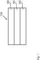
- Figure 1 shows a diode 100 which comprises a first 102 and a second electrode 106, a semiconducting 104 layer comprising semiconducting particles at least partly embedded and a mixture of glycerol and cellulose based material, wherein said cellulose based material is nano-fibrillated cellulose (NFC).
- the first 102 and second electrodes 106 and the semiconductor layer 104 are at least partially stacked on top of each other in a first direction. Hence the semiconducting layer 104 is sandwiched in between the first 102 and the second electrode 106.
- the amount of glycerol present in the semiconducting layer is in the range of 5 wt% to 75 wt%, and the amount of nano-fibrillated cellulose (NFC) present in the semiconducting layer is in the range of 10 wt % to 50 wt%.
- NFC nano-fibrillated cellulose
- the overall diode performance is mainly dependent on the properties of the interfaces between the first electrode and the semiconducting layer as well as between the semiconducting layer and the second electrode; the diode could have any shape in the plane not shown in Figure 1 . Actually, it may be sufficient that just one semiconducting particle is in contact with both the first and the second electrode.
- the resulting current throughput and rectification ratio of the diode device is mainly influenced by the doping level and, hence, the bulk conductivity of the semiconducting particles, the thickness of the oxide layers, and the energy barriers at the interfaces. Furthermore, the defect levels, the vertical and lateral conductivity in the first and second electrodes as well as the lateral conductivity in any assisting electrode come second in the set of parameters that affect the current throughput and rectification ratio.
- FIG. 2 shows a diode 200 in accordance with at least one embodiment of the invention.
- a first electrode 204 is provided on top of a substrate 202, e.g. PET.
- This first electrode 204 can also be referred to as the bottom electrode of the diode.
- the first electrode 204 can for example be an aluminium electrode.
- This semiconducting layer 206 comprises semiconducting particles 208, NFC 210 and glycerol.
- the semiconducting layer 206 partly covers the first electrode 204.
- the contact between the first electrode 204 and the semiconducting layer 206 may be a Schottky contact.
- the second electrode 212 is a nickel-coated carbon tape; which is supplied with electrons via a powering member 215 made of e.g. aluminium.
- the contact between the semiconducting layer and the second electrode may be an Ohmic contact, or at least a non-rectifying contact.
- the second electrode 212 may be covered by an assisting electrode, e.g. aluminium foil 214.
- the semiconducting particles 208 form a layer in said semiconducting layer 206 where single semiconducting particles are in contact with both the bottom and the top electrode. When the particles are arranged in such a layer a majority of the semiconducting particles that is in direct contact with the first electrode 204 may also be in contact with the second electrode 212. It should be understood that the layer portion, where single semiconducting particles are in contact with both the bottom and the top electrode, is arranged at least where the two electrodes overlap each other in the vertical direction. The portion where the two electrodes overlap each other in the vertical direction is indicated by reference numeral 220.
- the thickness of the semiconducting layer 206 is in the range of 5 ⁇ m to 100 ⁇ m.
- the glycerol in the semi-conducting layer makes the semi-conducting layer self-adhesive.
- the NFC in the semi-conducting layer makes the semi-conducting layer self-supporting.
- Figure 3 shows several examples of the aluminium bottom electrode according to at least one example embodiment of the invention. The different examples show how the aluminium pattern of the bottom electrode can be altered.
- the width of the bottom electrode 304, in the y direction is 50 ⁇ m, 75 ⁇ m, 100 ⁇ m ,and 200 ⁇ m, respectively.
- the elements indicated with 304 and 315 corresponds to layer 204 and 215, respectively, in Figure 2 .
- Figure 4 is SEM micrographs of the semiconducting layer in accordance with at least one example embodiment of the invention; the inset in the upper right corner shows a self-supporting NFC:glycerol:Si film that is being removed from the Petri dish, while (a) and (b) are the SEM images from the top and the bottom surfaces of the film, respectively.
- Figure 5 shows a frequency response curve of a representative diode according to at least one embodiment of the present invention.
- This particular example of a diode according to at least one example embodiment of the invention shows a cut-out frequency of 1.8 GHz, but the diode still produces a DC output voltage greater than 1 V at 3 GHz.
- the input power applied is 77 mW, which corresponds to an input power that can be supplied from a mobile phone held in a close proximity to the diode when making a call within the GSM band.
- Figure 6A shows a current-voltage-curve on a linear scale of a representative diode according to at least one example embodiment of the invention.
- Figure 6B shows a current-voltage curve on a semi-log scale of the same representative diode according to at least one example embodiment of the present invention.
- the dashed lines in Figures 6A and 6B represent results of a printed diode manufactured as described in Sani et al. (All-printed diode operating at 1.6 GHz; PNAS, 2014, 111, 11943-11948 ).
- Material preparation For preparation of Si- ⁇ Ps, a single crystal Si wafer with a resistivity of 0.01-0.02 ⁇ cm and doped with Sb is used. First, the wafer is crushed and then milled for 2 hours in a Retsch PM100 ball milling machine. The obtained particles are further fractioned using a Retsch sieve machine with a 100 ⁇ m stainless steel sieve, where particles that passes the sieve, also referred to as ⁇ Ps, are collected and used for the diode manufacturing process. An aqueous dispersion of anionic NFC gel was prepared by high-pressure homogenization of carboxylethylated cellulose fibers and consecutively by an ultrasonication centrifugation process. The resulting cellulose nanofibrils typically have a diameter of 5-60 nm and their length vary from 100 nm to several ⁇ m.
- Preparation of the film The fractioned Si powder is then mixed with 0.5 wt% NFC water suspension and glycerol; the latter ingredient is included to enhance the surface adhesion of the dried film.
- the mixture is then further diluted with water by a factor of two and thoroughly mixed with a shear mixer for 3 minutes, and then further mixed with an ultrasonic gun (Sonopuls 2200) by applying 1 s pulses, at a 10% duty cycle, with 20 W power for 30-60 s. 5 g of the final mixture is cast into a petri dish with a diameter of 50 mm and is then left to dry in ambient environment.
- the resulting dried film contains 12.5 wt% Si- ⁇ Ps, 51.5 wt% glycerol and 36 wt% NFC.
- the resulting films also referred to as NFC:Si- ⁇ P film or NFC:Si- ⁇ P composite film, can easily be peeled off from the bottom of the Petri dishes.
- the surfaces of the two sides of the NFC:Si film were characterized by optical profilometer and scanning electron microscope (SEM), see Figure 4 . It can be seen that even though a sieve for 100 ⁇ m large particles was used, the largest particles are not larger than 50 ⁇ m.
- the diode structure is simply fabricated by laminating and pressing the different layers of materials together. The only equipment used is a calender machine working at room temperature. A flexible substrate composed of 9 ⁇ m Al foil laminated onto a 36 ⁇ m PET foil was used. The Al substrate is patterned by a photolithography process, where the pattern was defined and etched by photoresist and buffered phosphoric acid, respectively. A piece of the NFC:Si- ⁇ Ps composite film is then cut and pasted onto a e.g. 1 mm wide Al strip on the pre-patterned Al substrate. The structure is then pressed using a calender machine, with a pressure of 3 bar, which ensures good contact between the Al strip and the NFC:Si- ⁇ P film.
- the entire PET/Al/NFC:Si- ⁇ P film/Ni/C/Al stack structure is pressed once more using the calender machine, again with a pressure of 3 bar.
- the overlapping surface area of the Si film and the top electrode is 2 mm 2 .
- a diode structure was created by incorporating the NFC:Si- ⁇ P film between AI/PET and a conductive tape by using a simple "peel and stick" assembly method. Schottky junctions are formed between the Si particles and the Al bottom electrode, while the non-rectifying, close to ohmic, contact is ensured by a double adhesive conductive tape based on Ni plated carbon fibers.
- One of the prime advantages of using this kind of contact electrodes over the common conductive inks, such as carbon paste, is that the conductive tape cannot penetrate into, or even through, the semiconducting layer to cause short circuits down to the bottom contact.
- Another function of the Ni/C tape is that it spans over the junction area and attaches to the PET substrate, i.e. it ensures a mechanically stable diode that is kept in place.
- the entire process of fabricating both the semiconducting NFC:Si- ⁇ P composite film and the diode is performed at room temperature.
- the only machine used in this process is a calender machine that presses and laminates the different layers/films together.
- the high frequency performance of the diodes is characterized by applying a single harmonic signal, and the output DC voltage is then measured within a span of frequencies ranging from 10 MHz to 6 GHz.
- An Agilent RF frequency signal generator 8665B is connected to the sample via a 50 ⁇ cable and a microwave Air Coplanar Probe (ACP) from Cascade Microtech (custom made with 1250 ⁇ m pitch between ground and signal probe tips), and the output signal of the sample is also probed with an ACP and connected with a 50 ⁇ cable to an oscilloscope (Tektronix TDS3034) with the input impedance of 1 M ⁇ and 13 pF.
- ACP microwave Air Coplanar Probe
- the sample was connected to an input power of 19.9 dBm via a 1 dB attenuator in order to reduce signal reflections.
- a set-up similar to the high frequency measurement is used, but a resistive load is connected in series to the diode instead of the oscilloscope.
- the voltage drop across the resistive load is measured at input frequencies of 0.9 and 1.8 GHz while the load is varied between 50 ⁇ and 1 M ⁇ .
- the NFC:Si- ⁇ P films are entirely self-supporting and semitransparent, and can easily be peeled off from the petri dish by using ordinary tweezers.
- the film is slightly sticky and exhibit self-adhesive surface properties due to the presence of glycerol.
- the bottom surface i.e. the side that is in contact with the Petri dish surface during drying, is relatively more adhesive than the top surface. This probably indicates that there is a slightly higher glycerol content at the bottom section of the film as compared to the top volume.
- SEM images, Figure 4 showed that although the sieve used to filter the Si particles is 100 ⁇ m, the crossing line lengths of the largest particles are shorter than 50 ⁇ m.
- the NFC matrix has a thickness of 10-15 ⁇ m according to the optical profilometer measurements.
- the SEM images showed that all Si- ⁇ Ps are covered with NFC along the top surface. This NFC top-layer is probably very thin for the larger Si- ⁇ Ps that are extending outside the NFC film matrix; while at the bottom surface many of the particles are not covered by NFC.
- the SEM images taken from the top surface of the films before and after they are pressed using the calender machine suggest that the mechanical pressure during calendering might cause the thin NFC layer to rupture, and thereby ensuring good electrical contact between the Si- ⁇ Ps and the electrodes.
- the Si- ⁇ Ps embedded in the NFC film form Schottky contacts to the Al bottom layer.
- the nature of the contact between a NFC:Si- ⁇ P film and the Ni/C tape electrode is ohmic, or close to ohmic, or at least non-rectifying. This was confirmed by I-V measurements performed on a symmetric structure of the film sandwiched between two layers of Ni/C tape.
- the use of an extra Al foil on top of the Ni/C tape enhances the lateral conductivity of the top contact, which bridges between the top side of the semiconducting film and the electrode (315 in Figure 3 ) on the substrate.
- Diode performance and modeling In all the measurements and modeling the current level is here the preferred description of the charge transport through the device over the current density. This is because the semiconducting layer of the diode is heterogeneous and consists of multiple particles, which together contributes in parallel to the resulting measured current. Also, each particle contributes differently to the electrical conduction depending on its shape, orientation, size, etc., therefore the current density would not be an accurate term to use for this device structure.
- the device has a sharp turn-on voltage at around 0.5 V, and a rectification ratio up to 4x10 3 is achieved below 2 V bias.
- a good Schottky contact is established between the Al bottom electrode and the Si particles.
- the leakage current increases, resulting in lower rectification factor.
- the relatively high leakage current is probably due to the Schottky barrier lowering and defect levels on the surface of the particles.
- the diode performance is still sufficient in e.g. many low-power (mW range) energy harvesting applications.
- two have a current level on the order of 10 -5 A two have about 10 -3 A and two have 10 -2 A of forward current at 2 V.
- I s is the reverse current
- R s is the series resistance
- n is the ideality factor of the diode
- q and T are the elementary charge and the absolute temperature, respectively.
- the ideality factor which equals 1 for an ideal diode, is an indication of the voltage dependence of the barrier height.
- the y-axis intercept of the linear part of the logarithmic-linear plot of the I-V curve gives the reverse current and the ideality factor can be calculated using the slope of the same curve.
- the possibility of reconfiguring the sticker label diode was successfully tested. It was possible to lift off the upper part of the diode consisting of the NFC:Si- ⁇ P film laminated with the Ni/C conductive tape. This part of the diode stack was then transferred to another substrate, and after an additional calendering process step a new diode with similar I-V performance, as compared to the initial diode, was obtained.
- the cut-off frequency of the device is defined as the frequency where the output power drops to half (or equivalently the voltage drops to 1 / 2 ) of the corresponding value at the lowest frequency (10 MHz in our measurement).
- the frequency response of a representative diode shows a cut-off frequency of 1.8 GHz even though the diode still produces a DC output voltage greater than 1 V at 3 GHz.
- the applied input power is 18.9 dBm (77 mW, after subtracting the damping effect from the attenuator), and this is a power that can be supplied for example by a mobile phone that is held in close proximity to the diode while making a call within the GSM band.
- two of them have a cut-off frequency above 1 GHz. However all of the devices have at least a cut-off frequency of 100 MHz.
- the overlapping surface area of the two electrodes sandwiching the NFC:Si- ⁇ P film is 2 mm 2 .
- the surface area of the Schottky contact is, however, much smaller as compared to the projected surface area of the particles since only a fraction of the surface area of each particle is in contact with the Al substrate.
- the output power for a resistive load is measured at two fixed frequencies, 0.9 GHz and 1.8 GHz, which correspond to the two GSM frequencies, by using the same set-up and input power as in the frequency response measurement.
- a variable load resistor is connected to the circuit and the output power is measured while the load resistance is varied between 50 ⁇ to 1 M ⁇ at a constant input power of 77 mW.
- the load resistance is increased, the voltage drop across the load is also increased while the current simultaneously drops.
- the power which is the product of current and voltage, is low as long as the resistance is very low (i.e., close to short circuit), since the voltage drop is small.
- Adjusting the load resistance to a very high value also results in a low output power since the current is negligible.
- the output power has a peak when the resistance of the load is equal to the real part of the output impedance, which for this diode appears to be 800 ⁇ and 1400 ⁇ at the input frequencies of 0.9 MHz and 1.8 MHz, respectively.
- the maximum output power available with the mentioned input is around 1.26 mW at 0.9 GHz and 0.25 mW at 1.8 GHz. Although these values are relatively low as compared to commercial diodes, they are sufficient for powering low input power devices such as printed organic electrochromic displays and sensors. It should be noted that the maximum output power is reached only when the impedance of the load matches the output impedance of the entire measurement circuit, including the diode, which is however not purely resistive.
Landscapes
- Engineering & Computer Science (AREA)
- Manufacturing & Machinery (AREA)
- Electrodes Of Semiconductors (AREA)
- Conductive Materials (AREA)
Claims (14)
- Diode, umfassend:- eine erste und eine zweite Elektrode;- eine halbleitende Schicht, die halbleitende Partikel, die wenigstens teilweise in einem Gemisch aus Glycerin und einem Material auf Cellulosebasis eingebettet sind, umfasst, wobei die Größe der halbleitenden Partikel in wenigstens einer ersten Richtung größer als 5 µm und kleiner als 100 µm ist, wobei das Material auf Cellulosebasis nanofibrillierte Cellulose (NFC) ist;wobei die erste und zweite Elektrode und die Halbleiterschicht in einer ersten Richtung wenigstens teilweise aufeinander geschichtet sind;
wobei die Menge an Glycerin, die in der halbleitenden Schicht vorhanden ist, im Bereich von 5 Gew.% bis 75 Gew.% liegt und die Menge an nanofibrillierter Cellulose (NFC), die in der halbleitenden Schicht vorhanden ist, im Bereich von 10 Gew.% bis 50 Gew.% liegt und wobei die halbleitenden Partikel eine einzige Schicht in der halbleitenden Schicht ausbilden und wobei ein Großteil der halbleitenden Partikel sowohl mit der unteren als auch mit der oberen Elektrode in direktem Kontakt steht. - Diode nach Anspruch 1, wobei die Menge an Glycerin, die in der halbleitenden Schicht vorhanden ist, im Bereich von 5 Gew. % bis 75 Gew.% oder 10 Gew.% bis 75 Gew.% oder 15 Gew.% bis 70 Gew.% oder 25 Gew.% bis 60 Gew.% liegt.
- Diode nach Anspruch 1 oder 2, wobei die Menge an nanofibrillierter Cellulose (NFC), die in der halbleitenden Schicht vorhanden ist, im Bereich von 10 Gew.% bis 50 Gew.% oder 15 Gew.% bis 45 Gew.% oder 25 Gew.% bis 40 Gew.% liegt.
- Diode nach einem der vorhergehenden Ansprüche, wobei die Menge an halbleitenden Partikeln im Bereich von 0,1 Gew.% bis 85 Gew.% oder 1 Gew.% bis 60 Gew.% oder 5 Gew.% bis 30 Gew.% oder 10 Gew.% bis 20 Gew.% liegt.
- Diode nach einem der vorhergehenden Ansprüche, wobei das Glycerin, das Material auf Cellulosebasis und die halbleitenden Partikel 75 Gew.% oder 85 Gew.% oder 95 Gew.% der halbleitenden Schicht ausmachen.
- Diode nach einem der vorhergehenden Ansprüche, wobei das halbleitende Material in einer Partikelform mit Partikeln, die in wenigstens einer Richtung größer als 10 µm oder größer als 15 µm sind, bereitgestellt ist.
- Diode nach einem der vorhergehenden Ansprüche, wobei die lonenleitfähigkeit der halbleitenden Schicht niedriger als 1E-4 S/cm oder niedriger als 1E-5 S/cm oder niedriger als 1E-6 S/cm ist.
- Diode nach Anspruch 1;
wobei die Größe der halbleitenden Partikel in wenigstens der ersten Richtung kleiner als 50 µm ist. - Diode nach einem der vorhergehenden Ansprüche, wobei die halbleitenden Partikel aus der Gruppe IV oder III ausgewählt sind; oder wobei die halbleitenden Partikel aus der Gruppe IV oder III in einem Gemisch mit Elementen der Gruppe V ausgewählt sind; oder wobei die halbleitenden Partikel aus einer Gruppe bestehend aus Si, Ge, AlP, AlAs, GaN, GaAs, InN, InP und InAs ausgewählt sind; oder wobei es sich bei den halbleitenden Partikeln um n- oder p-dotiertes Silicium handelt.
- Diode nach einem der vorhergehenden Ansprüche, wobei die erste Elektrode Metall umfasst oder wobei die erste Elektrode Aluminium, Silber oder Kombinationen davon umfasst.
- Diode nach einem der vorhergehenden Ansprüche, wobei die zweite Elektrode ein Metall, elektrisch leitende Polymere, Materialien auf Kohlenstoffbasis oder Kombinationen davon umfasst.
- Verfahren zur Bereitstellung einer Diode nach Anspruch 1, das folgende Schritte umfasst:- Bereitstellen eines Substrats, auf dem eine erste Elektrode angeordnet ist,- Bereitstellen einer halbleitenden Schicht in physischem Kontakt mit und wenigstens teilweise auf der ersten Elektrode, wobei die Schicht bereitgestellt wird, indem zunächst eine Lösung aus Glycerin, NFC und halbleitenden Partikeln hergestellt wird, wobei die halbleitende Schicht halbleitende Partikel umfasst, die in wenigstens einer ersten Richtung größer als 5 µm und kleiner als 100 µm sind,- Formen wenigstens eines Teils der Lösung zu einer Schicht und danach Trocknen der Schicht; wobei die getrocknete halbleitende Schicht Glycerin im Bereich von 5 Gew. % bis 75 Gew. % und nanofibrillierte Cellulose (NFC) im Bereich von 10 Gew. % bis 50 Gew. % umfasst,- Bereitstellen einer zweiten Elektrode in physischem Kontakt mit und wenigstens teilweise auf der halbleitenden Schicht, wobei die halbleitenden Partikel eine einzige Schicht in der halbleitenden Schicht ausbilden und wobei ein Großteil der halbleitenden Partikel sowohl mit der unteren als auch mit der oberen Elektrode in direktem Kontakt steht.
- Verfahren nach Anspruch 12, wobei die getrocknete halbleitende Schicht selbstklebend ist;
und wobei der Schritt des Bereitstellens der halbleitenden Schicht in physischem Kontakt mit der ersten Elektrode ein Anbringen der halbleitenden Schicht an der ersten Elektrode unter Ausnutzung des Selbstklebevermögens umfasst. - Verfahren nach Anspruch 12 oder 13, wobei der Schritt des Formens der halbleitenden Schicht ein Benutzen eines Gießprozesses beim Formen der halbleitenden Schicht umfasst.
Applications Claiming Priority (1)
| Application Number | Priority Date | Filing Date | Title |
|---|---|---|---|
| SE1650220A SE540484C2 (en) | 2016-02-19 | 2016-02-19 | Diode and method for producing the same |
Publications (2)
| Publication Number | Publication Date |
|---|---|
| EP3208852A1 EP3208852A1 (de) | 2017-08-23 |
| EP3208852B1 true EP3208852B1 (de) | 2019-03-27 |
Family
ID=58094257
Family Applications (1)
| Application Number | Title | Priority Date | Filing Date |
|---|---|---|---|
| EP17156691.2A Active EP3208852B1 (de) | 2016-02-19 | 2017-02-17 | Diode und verfahren zur herstellung davon |
Country Status (2)
| Country | Link |
|---|---|
| EP (1) | EP3208852B1 (de) |
| SE (1) | SE540484C2 (de) |
Cited By (2)
| Publication number | Priority date | Publication date | Assignee | Title |
|---|---|---|---|---|
| CN110098346A (zh) * | 2019-04-26 | 2019-08-06 | 深圳市华星光电半导体显示技术有限公司 | 显示面板的封装结构及其封装方法 |
| WO2025221193A1 (en) | 2024-04-19 | 2025-10-23 | Rise Research Institutes of Sweden AB | An electronic device and method for its production |
Family Cites Families (1)
| Publication number | Priority date | Publication date | Assignee | Title |
|---|---|---|---|---|
| EP2800102B1 (de) * | 2013-04-30 | 2018-05-23 | RISE Acreo AB | Selbstklebende leitfähige Schicht |
-
2016
- 2016-02-19 SE SE1650220A patent/SE540484C2/en unknown
-
2017
- 2017-02-17 EP EP17156691.2A patent/EP3208852B1/de active Active
Non-Patent Citations (1)
| Title |
|---|
| None * |
Cited By (2)
| Publication number | Priority date | Publication date | Assignee | Title |
|---|---|---|---|---|
| CN110098346A (zh) * | 2019-04-26 | 2019-08-06 | 深圳市华星光电半导体显示技术有限公司 | 显示面板的封装结构及其封装方法 |
| WO2025221193A1 (en) | 2024-04-19 | 2025-10-23 | Rise Research Institutes of Sweden AB | An electronic device and method for its production |
Also Published As
| Publication number | Publication date |
|---|---|
| EP3208852A1 (de) | 2017-08-23 |
| SE540484C2 (en) | 2018-09-25 |
| SE1650220A1 (en) | 2017-08-20 |
Similar Documents
| Publication | Publication Date | Title |
|---|---|---|
| Krishnan et al. | Design and development of batch fabricatable metal–insulator–metal diode and microstrip slot antenna as rectenna elements | |
| Sani et al. | Flexible lamination-fabricated ultra-high frequency diodes based on self-supporting semiconducting composite film of silicon micro-particles and nano-fibrillated cellulose | |
| KR101982177B1 (ko) | 압력센서, 그를 포함하는 압력센서 매트릭스 어레이 및 그의 제조방법 | |
| EP3208852A1 (de) | Diode und verfahren zur herstellung davon | |
| JP2001159569A (ja) | 感圧センサ | |
| Clochiatti et al. | Broadband THz detection using InP triple-barrier resonant tunneling diode with integrated antenna | |
| Edberg et al. | Electrochemical circuits from ‘cut and stick’PEDOT: PSS-nanocellulose composite | |
| WO2016204882A2 (en) | Biodegradable microwave electronic devices | |
| US12437934B2 (en) | Capacitor with negative electrode foil including carbon layer | |
| CN116130529A (zh) | 一种具有宽频光电响应的探测器件及其制备方法 | |
| Kaur et al. | Study of microwave circuits based on Metal-Insulator-Metal (MIM) diodes on flex substrates | |
| CN220606158U (zh) | 薄膜型的t型热电偶 | |
| CN103262252A (zh) | 二极管,其用途,及其制备方法 | |
| Matsunaga et al. | 5.8-GHz stacked differential mode rectenna suitable for large-scale rectenna arrays | |
| Sadek et al. | 10 GHz Compact Shunt-Diode Rectifier Circuit Using Thin Film Ag/AZO Schottky Barrier Diode for Energy Harvesting Applications | |
| Han et al. | ITO Schottky diode wth record f T beyond 400 GHz: Exploring thickness depdendant film property and novel heterogeneous design | |
| US11056796B2 (en) | Directly flat-attached switching component for active frequency selective surface and fabricating method thereof | |
| Etor et al. | Improving power transfer in rectenna via impedance matching at GHz frequencies | |
| US20150303376A1 (en) | Memristive rf switches | |
| JP2013219389A (ja) | 太陽電池セル及び該太陽電池セルを備えた太陽電池モジュール | |
| EP3613095A1 (de) | Segmentierte elektrodeneinheit, batterie und verfahren zum herstellen einer segmentierten elektrodeneinheit | |
| US20110126880A1 (en) | Thin-Film Photovoltaic Panel and Method of Producing the Same | |
| Ando et al. | Fabrication of low-threshold discreet Schottky barrier diode using natural pyrite crystal | |
| WO2025221193A1 (en) | An electronic device and method for its production | |
| Fatima et al. | Design of FSS Based RF Energy Harvesting System With Near Unity Absorption |
Legal Events
| Date | Code | Title | Description |
|---|---|---|---|
| PUAI | Public reference made under article 153(3) epc to a published international application that has entered the european phase |
Free format text: ORIGINAL CODE: 0009012 |
|
| STAA | Information on the status of an ep patent application or granted ep patent |
Free format text: STATUS: THE APPLICATION HAS BEEN PUBLISHED |
|
| AK | Designated contracting states |
Kind code of ref document: A1 Designated state(s): AL AT BE BG CH CY CZ DE DK EE ES FI FR GB GR HR HU IE IS IT LI LT LU LV MC MK MT NL NO PL PT RO RS SE SI SK SM TR |
|
| AX | Request for extension of the european patent |
Extension state: BA ME |
|
| STAA | Information on the status of an ep patent application or granted ep patent |
Free format text: STATUS: REQUEST FOR EXAMINATION WAS MADE |
|
| 17P | Request for examination filed |
Effective date: 20180222 |
|
| RBV | Designated contracting states (corrected) |
Designated state(s): AL AT BE BG CH CY CZ DE DK EE ES FI FR GB GR HR HU IE IS IT LI LT LU LV MC MK MT NL NO PL PT RO RS SE SI SK SM TR |
|
| GRAP | Despatch of communication of intention to grant a patent |
Free format text: ORIGINAL CODE: EPIDOSNIGR1 |
|
| STAA | Information on the status of an ep patent application or granted ep patent |
Free format text: STATUS: GRANT OF PATENT IS INTENDED |
|
| INTG | Intention to grant announced |
Effective date: 20180913 |
|
| GRAS | Grant fee paid |
Free format text: ORIGINAL CODE: EPIDOSNIGR3 |
|
| GRAA | (expected) grant |
Free format text: ORIGINAL CODE: 0009210 |
|
| STAA | Information on the status of an ep patent application or granted ep patent |
Free format text: STATUS: THE PATENT HAS BEEN GRANTED |
|
| RAP1 | Party data changed (applicant data changed or rights of an application transferred) |
Owner name: RISE ACREO AB |
|
| AK | Designated contracting states |
Kind code of ref document: B1 Designated state(s): AL AT BE BG CH CY CZ DE DK EE ES FI FR GB GR HR HU IE IS IT LI LT LU LV MC MK MT NL NO PL PT RO RS SE SI SK SM TR |
|
| REG | Reference to a national code |
Ref country code: GB Ref legal event code: FG4D |
|
| REG | Reference to a national code |
Ref country code: CH Ref legal event code: EP |
|
| REG | Reference to a national code |
Ref country code: AT Ref legal event code: REF Ref document number: 1114055 Country of ref document: AT Kind code of ref document: T Effective date: 20190415 |
|
| REG | Reference to a national code |
Ref country code: IE Ref legal event code: FG4D |
|
| REG | Reference to a national code |
Ref country code: DE Ref legal event code: R096 Ref document number: 602017002865 Country of ref document: DE |
|
| PG25 | Lapsed in a contracting state [announced via postgrant information from national office to epo] |
Ref country code: FI Free format text: LAPSE BECAUSE OF FAILURE TO SUBMIT A TRANSLATION OF THE DESCRIPTION OR TO PAY THE FEE WITHIN THE PRESCRIBED TIME-LIMIT Effective date: 20190327 Ref country code: NO Free format text: LAPSE BECAUSE OF FAILURE TO SUBMIT A TRANSLATION OF THE DESCRIPTION OR TO PAY THE FEE WITHIN THE PRESCRIBED TIME-LIMIT Effective date: 20190627 Ref country code: SE Free format text: LAPSE BECAUSE OF FAILURE TO SUBMIT A TRANSLATION OF THE DESCRIPTION OR TO PAY THE FEE WITHIN THE PRESCRIBED TIME-LIMIT Effective date: 20190327 Ref country code: LT Free format text: LAPSE BECAUSE OF FAILURE TO SUBMIT A TRANSLATION OF THE DESCRIPTION OR TO PAY THE FEE WITHIN THE PRESCRIBED TIME-LIMIT Effective date: 20190327 |
|
| REG | Reference to a national code |
Ref country code: NL Ref legal event code: MP Effective date: 20190327 |
|
| PG25 | Lapsed in a contracting state [announced via postgrant information from national office to epo] |
Ref country code: LV Free format text: LAPSE BECAUSE OF FAILURE TO SUBMIT A TRANSLATION OF THE DESCRIPTION OR TO PAY THE FEE WITHIN THE PRESCRIBED TIME-LIMIT Effective date: 20190327 Ref country code: NL Free format text: LAPSE BECAUSE OF FAILURE TO SUBMIT A TRANSLATION OF THE DESCRIPTION OR TO PAY THE FEE WITHIN THE PRESCRIBED TIME-LIMIT Effective date: 20190327 Ref country code: HR Free format text: LAPSE BECAUSE OF FAILURE TO SUBMIT A TRANSLATION OF THE DESCRIPTION OR TO PAY THE FEE WITHIN THE PRESCRIBED TIME-LIMIT Effective date: 20190327 Ref country code: BG Free format text: LAPSE BECAUSE OF FAILURE TO SUBMIT A TRANSLATION OF THE DESCRIPTION OR TO PAY THE FEE WITHIN THE PRESCRIBED TIME-LIMIT Effective date: 20190627 Ref country code: GR Free format text: LAPSE BECAUSE OF FAILURE TO SUBMIT A TRANSLATION OF THE DESCRIPTION OR TO PAY THE FEE WITHIN THE PRESCRIBED TIME-LIMIT Effective date: 20190628 Ref country code: RS Free format text: LAPSE BECAUSE OF FAILURE TO SUBMIT A TRANSLATION OF THE DESCRIPTION OR TO PAY THE FEE WITHIN THE PRESCRIBED TIME-LIMIT Effective date: 20190327 |
|
| REG | Reference to a national code |
Ref country code: AT Ref legal event code: MK05 Ref document number: 1114055 Country of ref document: AT Kind code of ref document: T Effective date: 20190327 |
|
| PG25 | Lapsed in a contracting state [announced via postgrant information from national office to epo] |
Ref country code: ES Free format text: LAPSE BECAUSE OF FAILURE TO SUBMIT A TRANSLATION OF THE DESCRIPTION OR TO PAY THE FEE WITHIN THE PRESCRIBED TIME-LIMIT Effective date: 20190327 Ref country code: EE Free format text: LAPSE BECAUSE OF FAILURE TO SUBMIT A TRANSLATION OF THE DESCRIPTION OR TO PAY THE FEE WITHIN THE PRESCRIBED TIME-LIMIT Effective date: 20190327 Ref country code: CZ Free format text: LAPSE BECAUSE OF FAILURE TO SUBMIT A TRANSLATION OF THE DESCRIPTION OR TO PAY THE FEE WITHIN THE PRESCRIBED TIME-LIMIT Effective date: 20190327 Ref country code: RO Free format text: LAPSE BECAUSE OF FAILURE TO SUBMIT A TRANSLATION OF THE DESCRIPTION OR TO PAY THE FEE WITHIN THE PRESCRIBED TIME-LIMIT Effective date: 20190327 Ref country code: IT Free format text: LAPSE BECAUSE OF FAILURE TO SUBMIT A TRANSLATION OF THE DESCRIPTION OR TO PAY THE FEE WITHIN THE PRESCRIBED TIME-LIMIT Effective date: 20190327 Ref country code: PT Free format text: LAPSE BECAUSE OF FAILURE TO SUBMIT A TRANSLATION OF THE DESCRIPTION OR TO PAY THE FEE WITHIN THE PRESCRIBED TIME-LIMIT Effective date: 20190727 Ref country code: AL Free format text: LAPSE BECAUSE OF FAILURE TO SUBMIT A TRANSLATION OF THE DESCRIPTION OR TO PAY THE FEE WITHIN THE PRESCRIBED TIME-LIMIT Effective date: 20190327 Ref country code: SK Free format text: LAPSE BECAUSE OF FAILURE TO SUBMIT A TRANSLATION OF THE DESCRIPTION OR TO PAY THE FEE WITHIN THE PRESCRIBED TIME-LIMIT Effective date: 20190327 |
|
| PG25 | Lapsed in a contracting state [announced via postgrant information from national office to epo] |
Ref country code: SM Free format text: LAPSE BECAUSE OF FAILURE TO SUBMIT A TRANSLATION OF THE DESCRIPTION OR TO PAY THE FEE WITHIN THE PRESCRIBED TIME-LIMIT Effective date: 20190327 Ref country code: PL Free format text: LAPSE BECAUSE OF FAILURE TO SUBMIT A TRANSLATION OF THE DESCRIPTION OR TO PAY THE FEE WITHIN THE PRESCRIBED TIME-LIMIT Effective date: 20190327 |
|
| PG25 | Lapsed in a contracting state [announced via postgrant information from national office to epo] |
Ref country code: AT Free format text: LAPSE BECAUSE OF FAILURE TO SUBMIT A TRANSLATION OF THE DESCRIPTION OR TO PAY THE FEE WITHIN THE PRESCRIBED TIME-LIMIT Effective date: 20190327 Ref country code: IS Free format text: LAPSE BECAUSE OF FAILURE TO SUBMIT A TRANSLATION OF THE DESCRIPTION OR TO PAY THE FEE WITHIN THE PRESCRIBED TIME-LIMIT Effective date: 20190727 |
|
| REG | Reference to a national code |
Ref country code: DE Ref legal event code: R097 Ref document number: 602017002865 Country of ref document: DE |
|
| PG25 | Lapsed in a contracting state [announced via postgrant information from national office to epo] |
Ref country code: DK Free format text: LAPSE BECAUSE OF FAILURE TO SUBMIT A TRANSLATION OF THE DESCRIPTION OR TO PAY THE FEE WITHIN THE PRESCRIBED TIME-LIMIT Effective date: 20190327 |
|
| PLBE | No opposition filed within time limit |
Free format text: ORIGINAL CODE: 0009261 |
|
| STAA | Information on the status of an ep patent application or granted ep patent |
Free format text: STATUS: NO OPPOSITION FILED WITHIN TIME LIMIT |
|
| PG25 | Lapsed in a contracting state [announced via postgrant information from national office to epo] |
Ref country code: SI Free format text: LAPSE BECAUSE OF FAILURE TO SUBMIT A TRANSLATION OF THE DESCRIPTION OR TO PAY THE FEE WITHIN THE PRESCRIBED TIME-LIMIT Effective date: 20190327 |
|
| 26N | No opposition filed |
Effective date: 20200103 |
|
| PG25 | Lapsed in a contracting state [announced via postgrant information from national office to epo] |
Ref country code: TR Free format text: LAPSE BECAUSE OF FAILURE TO SUBMIT A TRANSLATION OF THE DESCRIPTION OR TO PAY THE FEE WITHIN THE PRESCRIBED TIME-LIMIT Effective date: 20190327 |
|
| REG | Reference to a national code |
Ref country code: CH Ref legal event code: PL |
|
| REG | Reference to a national code |
Ref country code: BE Ref legal event code: MM Effective date: 20200229 |
|
| PG25 | Lapsed in a contracting state [announced via postgrant information from national office to epo] |
Ref country code: MC Free format text: LAPSE BECAUSE OF FAILURE TO SUBMIT A TRANSLATION OF THE DESCRIPTION OR TO PAY THE FEE WITHIN THE PRESCRIBED TIME-LIMIT Effective date: 20190327 Ref country code: LU Free format text: LAPSE BECAUSE OF NON-PAYMENT OF DUE FEES Effective date: 20200217 |
|
| PG25 | Lapsed in a contracting state [announced via postgrant information from national office to epo] |
Ref country code: LI Free format text: LAPSE BECAUSE OF NON-PAYMENT OF DUE FEES Effective date: 20200229 Ref country code: CH Free format text: LAPSE BECAUSE OF NON-PAYMENT OF DUE FEES Effective date: 20200229 |
|
| PG25 | Lapsed in a contracting state [announced via postgrant information from national office to epo] |
Ref country code: IE Free format text: LAPSE BECAUSE OF NON-PAYMENT OF DUE FEES Effective date: 20200217 |
|
| PG25 | Lapsed in a contracting state [announced via postgrant information from national office to epo] |
Ref country code: BE Free format text: LAPSE BECAUSE OF NON-PAYMENT OF DUE FEES Effective date: 20200229 |
|
| PG25 | Lapsed in a contracting state [announced via postgrant information from national office to epo] |
Ref country code: MT Free format text: LAPSE BECAUSE OF FAILURE TO SUBMIT A TRANSLATION OF THE DESCRIPTION OR TO PAY THE FEE WITHIN THE PRESCRIBED TIME-LIMIT Effective date: 20190327 Ref country code: CY Free format text: LAPSE BECAUSE OF FAILURE TO SUBMIT A TRANSLATION OF THE DESCRIPTION OR TO PAY THE FEE WITHIN THE PRESCRIBED TIME-LIMIT Effective date: 20190327 |
|
| PG25 | Lapsed in a contracting state [announced via postgrant information from national office to epo] |
Ref country code: MK Free format text: LAPSE BECAUSE OF FAILURE TO SUBMIT A TRANSLATION OF THE DESCRIPTION OR TO PAY THE FEE WITHIN THE PRESCRIBED TIME-LIMIT Effective date: 20190327 |
|
| REG | Reference to a national code |
Ref country code: DE Ref legal event code: R079 Ref document number: 602017002865 Country of ref document: DE Free format text: PREVIOUS MAIN CLASS: H01L0029872000 Ipc: H10D0008600000 |
|
| PGFP | Annual fee paid to national office [announced via postgrant information from national office to epo] |
Ref country code: FR Payment date: 20241231 Year of fee payment: 9 |
|
| PGFP | Annual fee paid to national office [announced via postgrant information from national office to epo] |
Ref country code: DE Payment date: 20241231 Year of fee payment: 9 |
|
| PGFP | Annual fee paid to national office [announced via postgrant information from national office to epo] |
Ref country code: GB Payment date: 20250102 Year of fee payment: 9 |