EP3206215A1 - Photoelectric conversion device - Google Patents
Photoelectric conversion device Download PDFInfo
- Publication number
- EP3206215A1 EP3206215A1 EP17157359.5A EP17157359A EP3206215A1 EP 3206215 A1 EP3206215 A1 EP 3206215A1 EP 17157359 A EP17157359 A EP 17157359A EP 3206215 A1 EP3206215 A1 EP 3206215A1
- Authority
- EP
- European Patent Office
- Prior art keywords
- sealing portion
- resin
- electrode
- photoelectric conversion
- wiring
- Prior art date
- Legal status (The legal status is an assumption and is not a legal conclusion. Google has not performed a legal analysis and makes no representation as to the accuracy of the status listed.)
- Granted
Links
Images


Classifications
-
- H—ELECTRICITY
- H01—ELECTRIC ELEMENTS
- H01G—CAPACITORS; CAPACITORS, RECTIFIERS, DETECTORS, SWITCHING DEVICES OR LIGHT-SENSITIVE DEVICES, OF THE ELECTROLYTIC TYPE
- H01G9/00—Electrolytic capacitors, rectifiers, detectors, switching devices, light-sensitive or temperature-sensitive devices; Processes of their manufacture
- H01G9/20—Light-sensitive devices
- H01G9/2068—Panels or arrays of photoelectrochemical cells, e.g. photovoltaic modules based on photoelectrochemical cells
- H01G9/2077—Sealing arrangements, e.g. to prevent the leakage of the electrolyte
-
- H—ELECTRICITY
- H01—ELECTRIC ELEMENTS
- H01G—CAPACITORS; CAPACITORS, RECTIFIERS, DETECTORS, SWITCHING DEVICES OR LIGHT-SENSITIVE DEVICES, OF THE ELECTROLYTIC TYPE
- H01G9/00—Electrolytic capacitors, rectifiers, detectors, switching devices, light-sensitive or temperature-sensitive devices; Processes of their manufacture
- H01G9/20—Light-sensitive devices
- H01G9/2022—Light-sensitive devices characterized by he counter electrode
-
- H—ELECTRICITY
- H01—ELECTRIC ELEMENTS
- H01M—PROCESSES OR MEANS, e.g. BATTERIES, FOR THE DIRECT CONVERSION OF CHEMICAL ENERGY INTO ELECTRICAL ENERGY
- H01M14/00—Electrochemical current or voltage generators not provided for in groups H01M6/00 - H01M12/00; Manufacture thereof
- H01M14/005—Photoelectrochemical storage cells
-
- H—ELECTRICITY
- H01—ELECTRIC ELEMENTS
- H01M—PROCESSES OR MEANS, e.g. BATTERIES, FOR THE DIRECT CONVERSION OF CHEMICAL ENERGY INTO ELECTRICAL ENERGY
- H01M50/00—Constructional details or processes of manufacture of the non-active parts of electrochemical cells other than fuel cells, e.g. hybrid cells
- H01M50/10—Primary casings, jackets or wrappings of a single cell or a single battery
- H01M50/183—Sealing members
-
- H—ELECTRICITY
- H01—ELECTRIC ELEMENTS
- H01G—CAPACITORS; CAPACITORS, RECTIFIERS, DETECTORS, SWITCHING DEVICES OR LIGHT-SENSITIVE DEVICES, OF THE ELECTROLYTIC TYPE
- H01G9/00—Electrolytic capacitors, rectifiers, detectors, switching devices, light-sensitive or temperature-sensitive devices; Processes of their manufacture
- H01G9/20—Light-sensitive devices
- H01G9/2004—Light-sensitive devices characterised by the electrolyte, e.g. comprising an organic electrolyte
-
- H—ELECTRICITY
- H01—ELECTRIC ELEMENTS
- H01G—CAPACITORS; CAPACITORS, RECTIFIERS, DETECTORS, SWITCHING DEVICES OR LIGHT-SENSITIVE DEVICES, OF THE ELECTROLYTIC TYPE
- H01G9/00—Electrolytic capacitors, rectifiers, detectors, switching devices, light-sensitive or temperature-sensitive devices; Processes of their manufacture
- H01G9/20—Light-sensitive devices
- H01G9/2027—Light-sensitive devices comprising an oxide semiconductor electrode
- H01G9/2031—Light-sensitive devices comprising an oxide semiconductor electrode comprising titanium oxide, e.g. TiO2
-
- H—ELECTRICITY
- H01—ELECTRIC ELEMENTS
- H01G—CAPACITORS; CAPACITORS, RECTIFIERS, DETECTORS, SWITCHING DEVICES OR LIGHT-SENSITIVE DEVICES, OF THE ELECTROLYTIC TYPE
- H01G9/00—Electrolytic capacitors, rectifiers, detectors, switching devices, light-sensitive or temperature-sensitive devices; Processes of their manufacture
- H01G9/20—Light-sensitive devices
- H01G9/2059—Light-sensitive devices comprising an organic dye as the active light absorbing material, e.g. adsorbed on an electrode or dissolved in solution
-
- Y—GENERAL TAGGING OF NEW TECHNOLOGICAL DEVELOPMENTS; GENERAL TAGGING OF CROSS-SECTIONAL TECHNOLOGIES SPANNING OVER SEVERAL SECTIONS OF THE IPC; TECHNICAL SUBJECTS COVERED BY FORMER USPC CROSS-REFERENCE ART COLLECTIONS [XRACs] AND DIGESTS
- Y02—TECHNOLOGIES OR APPLICATIONS FOR MITIGATION OR ADAPTATION AGAINST CLIMATE CHANGE
- Y02E—REDUCTION OF GREENHOUSE GAS [GHG] EMISSIONS, RELATED TO ENERGY GENERATION, TRANSMISSION OR DISTRIBUTION
- Y02E10/00—Energy generation through renewable energy sources
- Y02E10/50—Photovoltaic [PV] energy
- Y02E10/542—Dye sensitized solar cells
Definitions
- Solar cells using silicon and dye-sensitized solar cells are known as photoelectric conversion devices.
- dye-sensitized solar cells have attracted attention since they are inexpensive and can obtain a high photoelectric conversion efficiency and various developments have been conducted toward further improvement in photoelectric conversion efficiency.
- the second resin may include at least one species selected from the group consisting of polyvinyl alcohol and an ethylene-vinyl alcohol copolymer.
- the photoelectric conversion device 100 is provided with a working electrode 1 and a counter electrode (second electrode) 2 disposed so as to be opposite the working electrode 1.
- the working electrode 1 supports a photosensitizing dye.
- An electrolytic solution 3 is disposed between the working electrode 1 and the counter electrode 2, and a sealing portion 4 is provided between the working electrode 1 and the counter electrode 2 around the electrolytic solution 3.
- a second resin 5 is provided so as to cover at least a boundary B1 of the sealing portion 4 and the counter electrode 2 and a boundary B4 of the sealing portion 4 and the working electrode 1.
- Examples of the material constituting the wiring protection layer 12 include inorganic insulating materials such as a lead-free transparent low-melting-point glass frit.
- the third resin examples include polyimides, fluororesins, resins cured by ultraviolet ray and also an acid-modified polyethylene, polyvinyl alcohol and an ethylene-vinyl alcohol copolymer.
- the acid-modified polyethylene means a compound obtained by random copolymerization, alternate copolymerization, block copolymerization, or graft copolymerization of polyethylene with an acid or compounds obtained by neutralization thereof with metal ions.
- an ethylene-methacrylic acid copolymer is obtained by copolymerization of ethylene and methacrylic acid and is an acid-modified polyethylene.
- An ionomer obtained by neutralization of an ethylene-methacrylic acid copolymer with metal ions is also an acid-modified polyethylene.
- the first resin be an acid-modified polyethylene.
- an acid-modified polyethylene is extremely stable against organic solvents contained in the electrolytic solution 3, physical properties of the first resin, such as flexibility and adhesive ability, can be maintained over a long period.
- an acid-modified polyethylene be an ethylene-methacrylic acid copolymer, an ionomer, or polyethylene modified by maleic anhydride.
- the polarity of the first resin is high, adhesion to the transparent electrode of the working electrode 1, counter electrode 2, or wiring portion 4A becomes even stronger.
- the first resin is a resin cured by ultraviolet ray
- the above-mentioned ultraviolet curable resin is cured by ultraviolet ray and the resin sealing portion 4B linking the inorganic sealing portion 204A and the working electrode 1 is obtained therebetween.
- the first resin is a water-soluble resin
- finger-touch drying is conducted at room temperature, then drying is performed under low-humidity atmosphere, and the resin sealing portion 4B linking the inorganic sealing portion 204A and the working electrode 1 is obtained therebetween.
- the sealing ability of the wiring portion 4A and the inorganic sealing portion 204A with respect to the electrolytic solution 3 is also higher than that of the resin sealing portion 4B. Therefore, variations in photoelectric conversion efficiency with time can be sufficiently inhibited.
- the position of the current-collecting wiring 11 is not limited to those in the first to eighth embodiments and may be different therefrom.
- a photoelectric conversion device was obtained in the same manner as in Example 4, except that Eval, which is an ethylene-vinyl alcohol copolymer, was used as the first resin constituting the resin sealing portion.
Abstract
Description
- The present invention relates to a photoelectric conversion device.
- Solar cells using silicon and dye-sensitized solar cells are known as photoelectric conversion devices. Among them, dye-sensitized solar cells have attracted attention since they are inexpensive and can obtain a high photoelectric conversion efficiency and various developments have been conducted toward further improvement in photoelectric conversion efficiency.
- A dye-sensitized solar cell typically includes a working electrode having a semiconductor electrode provided on a transparent conductor, a counter electrode, a photosensitizing dye supported on the semiconductor electrode of the working electrode, an electrolytic solution disposed between the working electrode and the counter electrode, and a sealing portion provided between the working electrode and the counter electrode and around the electrolytic solution as main constituent elements, and the electrolytic solution is constituted, for example, by an electrolytic solution including an oxidation-reduction system (redox pair) such as, for example, I-/I3 -.
- In such dye-sensitized solar cell, electrons in the photosensitizing dye are excited by the incident visible light, and the electrons are injected from the photosensitizing dye that has thus been excited into a conduction band of the semiconductor electrode and flow out to the external circuit. The electrons that have returned from the external circuit reduce triiodide ions (I3 -) into iodide ions (I-), the photosensitizing dye that has lost electrons and has been oxidized is re-reduced by the iodide ions (I-), and electric power is thus generated.
- As such dye-sensitized solar cell, a photoelectric chemical cell in which volatilization of the volatile solvent contained in the electrolytic solution can be prevented by heating and melting Himilan (trade name, manufactured by Du Pont-Mitsui Polychemicals Co., Ltd.), which is an ionomer, to seal the electrolytic solution has been generally suggested (see for example Patent Document 1).
- Further, a photoelectric chemical cell has also been suggested in which volatilization of the volatile solvent contained in the electrolytic solution can be prevented by heating and melting an ethylene-vinyl alcohol copolymer to seal the electrolytic solution for the reason that the gas barrier ability of the copolymer is higher than that of Himilan (see for example Patent Document 2).
- Further, in a dye-sensitized solar cell, a metal wiring is sometimes provided on the transparent conductor to take out a large current. When this metal wiring comes into contact with an electrolytic solution, corrosion occurs. For this reason, the metal wiring is covered with a wiring protection layer such as low-melting-point glass frit.
- As such dye-sensitized solar cell, a dye-sensitized solar cell in which a metal wiring is disposed inside the sealing portion by constituting the sealing portion by the metal wiring and low-melting-point glass surrounding the metal wiring and photoelectric conversion efficiency is thus increased is also known (see for example Patent Document 3).
- Patent Document 1: Japanese Patent Application Publication No.
2003-297446 - Patent Document 2: Japanese Patent Application Publication No.
2007-149652 - Patent Document 3: Japanese Patent Application Publication No.
2005-346971 - However, in the photoelectric chemical cells described in
Patent Documents - With the dye-sensitized solar cell described in
Patent Document 3, when a photoelectric conversion device is used under an environment with large variations in temperature, since the working electrode and counter electrode usually have different thermal expansion coefficients and the working electrode or counter electrode and the sealing material usually have different thermal expansion coefficients, stresses concentrate in the sealing material and peeling or damage such as cracks can occur in the sealing material. This can result in the leak of electrolytic solution, in particular the leak of organic solvent contained in the electrolytic solution. Therefore, although the dye-sensitized solar cell described inPatent Document 3 demonstrates high photoelectric conversion efficiency because the metal wiring is disposed inside the sealing portion, when the cell is used under an environment with large variations in temperature, variations in photoelectric conversion efficiency with time cannot be said to be at a sufficiently low level. - Accordingly, it is an object of the present invention to provide a photoelectric conversion device in which variations in photoelectric conversion efficiency with time can be sufficiently inhibited.
- As a result of conducting extensive studies on what causes the variations in photoelectric conversion efficiency with time to solve the above problems, the present inventors considered that what the leak of electrolytic solution, in particular the leak of the organic solvent contained in the electrolytic solution remains large is the main reason why the photoelectric conversion efficiency changes with time. After a great deal of consideration, the present inventors have found that the above-described problems can be solved by the following invention.
- Thus, the present invention is a photoelectric conversion device including: a pair of electrodes; an electrolytic solution disposed between the pair of electrodes; and a sealing portion that links the pair of electrodes and is provided around the electrolytic solution, wherein at least part of the sealing portion comprises at least one inorganic sealing portion constituted by an inorganic material and at least one resin sealing portion constituted by a material including a first resin, and the inorganic sealing portion and the resin sealing portion are disposed along a direction connecting the pair of electrodes.
- In this photoelectric conversion device, at least part of the sealing portion comprises at least one inorganic sealing portion and at least one resin sealing portion, and the inorganic sealing portion and the resin sealing portion are disposed along the direction connecting the pair of electrodes. Herein, the inorganic sealing portion is constituted by an inorganic material, and the resin sealing portion is constituted by a material including a first resin. Therefore, the inorganic sealing portion has sealing ability with respect to the electrolytic solution that is higher than that of the resin sealing portion. Further, in the photoelectric conversion device in accordance with the present invention, due to the presence of the inorganic sealing portion, it is possible to increase the ratio of the boundary surface of the inorganic sealing portion, which has high sealing ability with respect to the electrolytic solution, and the electrolytic solution in the boundary surface of the electrolytic solution and the sealing portion by comparison with that in the case in which the sealing portion is constituted only by the resin sealing portion.
- Further, when the photoelectric conversion device is placed under an environment with large temperature variations and the pair of the electrodes have different thermal expansion coefficients, even if stresses are applied to the sealing portion, these stresses are relaxed by the resin sealing portion. Therefore, concentration of stresses in the inorganic sealing portion can be inhibited. Therefore, the occurrence of damage such as cracks in the inorganic sealing portion can be prevented.
- Therefore, with the photoelectric conversion in accordance with the present invention, the leak of the electrolytic solution can be sufficiently inhibited and variations in photoelectric conversion efficiency with time can be sufficiently inhibited. As a result, an extended service life of the photoelectric conversion can be realized.
- In the abovementioned photoelectric conversion device, for example, one electrode of the pair of electrodes has a first electrode, and the other electrode has a second electrode, in the sealing portion, the inorganic sealing portion is fixed on the first electrode, and the resin sealing portion links the inorganic sealing portion and the second electrode.
- The abovementioned photoelectric conversion device may be configured such that one electrode of the pair of electrodes has a first electrode, and the other electrode has a second electrode, in the sealing portion, the resin sealing portion is fixed on the first electrode, and the inorganic sealing portion links the resin sealing portion and the second electrode.
- Further, the abovementioned photoelectric conversion device may be configured such that one electrode of the pair of electrodes has a first electrode, and the other electrode has a second electrode, in the sealing portion, the inorganic sealing portion is fixed on the first electrode and the second electrode, and the resin sealing portion links the inorganic sealing portion fixed on the first electrode and the inorganic sealing portion fixed on the second electrode.
- Furthermore, the abovementioned photoelectric conversion device may be configured such that one electrode of the pair of electrodes has a first electrode, and the other electrode has a second electrode, in the sealing portion, the resin sealing portion is fixed on the first electrode and the second electrode, and the inorganic resin sealing portion links the resin sealing portion fixed on the first electrode and the resin sealing portion fixed on the second electrode.
- Further, in the abovementioned photoelectric conversion device, it is preferred that one electrode of the pair of electrodes has a first electrode, the other electrode of the pair of electrodes has a second electrode, the inorganic sealing portion is constituted by a wiring portion fixed on the first electrode, the wiring portion has a current-collecting wiring constituted by an inorganic material and provided on the first electrode and a wiring protection layer covering the current-collecting wiring, and the first electrode is a transparent electrode.
- In this photoelectric conversion device, the electrolytic solution is disposed between the first electrode and the second electrode. Further, at least part of the sealing portion provided around the electrolytic solution has a wiring portion provided on the first electrode, which is a transparent electrode, and this wiring portion has a current-collecting wiring and a wiring protection layer that covers the current-collecting wiring. In other words, in at least part of the sealing portion, the current-collecting wiring is disposed as part of the sealing portion inside the sealing portion in a state of being protected by the wiring protection layer from the electrolytic solution. Thus, the current-collecting wiring is not provided on the side of the sealing portion that is opposite the side facing the outside and also not provided inside the sealing portion. Therefore, the surface area occupied by the current-collecting wiring and the sealing portion on the light incidence surface of the first electrode can be minimized and the amount of incident light blocked by the current-collecting wiring and the sealing portion can be minimized. Therefore, the light-receiving surface area can be enlarged and high photoelectric conversion efficiency can be obtained.
- Further, the sealing portion is provided with a wiring portion and a resin sealing portion, and the wiring portion and the resin sealing portion are disposed along the direction connecting the transparent electrode and the counter electrode. Herein, the resin sealing portion is constituted by a material including a first resin. Therefore, when the photoelectric conversion device is placed under an environment with large temperature variations and the transparent electrode and the counter electrode have different thermal expansion coefficients, or the transparent electrode, counter electrode, and wiring portion have different thermal expansion coefficients, even if stresses are applied to the sealing portion, these stresses are relaxed by the resin sealing portion. Therefore, concentration of stresses in the wiring portion can be inhibited. Thus, the occurrence of damage such as cracks in the wiring portion can be prevented. As a result, the leak of the electrolytic solution caused by damage of the wiring portion can be prevented and variations in photoelectric conversion efficiency with time can be sufficiently inhibited.
- Thus, with the above-described photoelectric conversion device, high photoelectric conversion efficiency can be obtained and variations in photoelectric conversion efficiency with time can be sufficiently inhibited even when the device is used under an environment with large temperature variations.
- Herein, it is preferred that the sealing portion further include an inorganic sealing portion composed of an inorganic material provided on the second electrode, and the resin sealing portion link the wiring portion and the inorganic sealing portion.
- In such photoelectric conversion device, the sealing ability of the wiring portion and the inorganic sealing portion in comparison with the electrolytic solution is higher than that of the resin sealing portion. Therefore, variations in photoelectric conversion efficiency with time can be more adequately inhibited.
- Further, the abovementioned photoelectric conversion device may be configured such that the second electrode is also a transparent electrode, at least part of the sealing portion further includes an inorganic sealing portion provided on the second electrode, and the inorganic sealing portion is constituted by an inorganic material and by a second wiring portion having a second current-collecting wiring provided on the second electrode and a second wiring protection layer covering the second current-collecting wiring, and the resin sealing portion links the wiring portion and the second wiring portion.
- In this case, since the second electrode is a transparent electrode, the photoelectric conversion portion receives light from both the first electrode side and the second electrode side. As a result, the photoelectric conversion efficiency can be further increased. Further, since the second current-collecting wiring is disposed as part of the sealing portion inside the sealing portion, the incident light blocked by the second current-collecting wiring and the sealing portion can be minimized and the photoelectric conversion efficiency may be further increased.
- The abovementioned photoelectric conversion device may be configured such that one electrode of the pair of electrodes further has a photoelectric conversion portion that is in contact with the electrolytic solution, a working electrode is formed by the first electrode and the photoelectric conversion portion, and a counter electrode is formed by the second electrode.
- Further, the abovementioned photoelectric conversion device may be configured such that the other electrode of the pair of electrodes further has a photoelectric conversion portion that is in contact with the electrolytic solution, a working electrode is formed by the second electrode and the photoelectric conversion portion, and a counter electrode is formed by the first electrode.
- Further, the abovementioned photoelectric conversion device may be configured such that one electrode of the pair of electrodes includes a first electrode and a photoelectric conversion portion that is provided on the first electrode and is in contact with the electrolytic solution, the photoelectric conversion device further includes a wiring portion provided on the first electrode and between the sealing portion and the photoelectric conversion portion, and the wiring portion is constituted by an inorganic material and has a current-collecting wiring provided on the first electrode and a wiring protection layer covering the current-collecting wiring.
- Herein, it is preferred that a width of the inorganic sealing portion be less than a width of the wiring portion. In this case, it is possible to make the light-receiving surface area, that is, an aperture ratio, larger.
- Further, in the abovementioned photoelectric conversion device, it is preferred that one electrode of the pair of electrodes include a first electrode and a photoelectric conversion portion that is provided on the first electrode and is in contact with the electrolytic solution, the photoelectric conversion device further include a wiring portion provided on an opposite side of the photoelectric conversion portion to the sealing portion, on the first electrode, and the wiring portion be composed of a current-collecting wiring constituted by an inorganic material and provided on the first electrode.
- Herein, it is preferred that a width of the inorganic sealing portion be less than a width of the wiring portion. In this case, it is possible to make the light-receiving surface area, that is, an aperture ratio in the photoelectric conversion device larger.
- Further, in the abovementioned photoelectric conversion device, it is preferred that a second resin that at least covers a boundary of the sealing portion and the first electrode, a boundary of the sealing portion and the second electrode, and a boundary of the inorganic sealing portion and the resin sealing portion be provided on an opposite side of the sealing portion to the electrolytic solution. In this case, the leak of electrolytic solution is inhibited not only by the resin sealing portion, but also by the second resin. In particular, the interface leak of electrolytic solution through the interface of the sealing portion and the first electrode, interface of the sealing portion and the second electrode, and interface of the inorganic sealing portion and the resin sealing portion is effectively inhibited by the second resin.
- The second resin preferably includes at least one species selected from the group consisting of an acid-modified polyethylene and a resin cured by ultraviolet ray.
- When an acid-modified polyethylene or a resin cured by ultraviolet ray is used as the second resin, the bonding strength of the first electrode, second electrode, inorganic sealing portion, or first resin with the second resin is increased and the leak of the electrolytic solution on the respective interfaces can be inhibited.
- The second resin may include at least one species selected from the group consisting of polyvinyl alcohol and an ethylene-vinyl alcohol copolymer.
- When polyvinyl alcohol or an ethylene-vinyl alcohol copolymer is used as the second resin, since these resins have high gas barrier ability, the leak of the electrolytic solution in the second resin can be inhibited. Further, when the first resin includes at least one species of polyvinyl alcohol and an ethylene-vinyl alcohol copolymer, by ensuring the presence of a very small amount of water on the interface of the first resin and second resin, the two resins dissolve and bond mutually in the vicinity of the interface. Therefore, the leak of the electrolytic solution is inhibited even more effectively.
- The first resin preferably includes at least one species selected from the group consisting of an acid-modified polyethylene and a resin cured by ultraviolet ray. When an acid-modified polyethylene or a resin cured by ultraviolet ray is used as the first resin, the bonding strength of the first electrode, second electrode, or inorganic sealing portion with the first resin is increased and the leak of the electrolytic solution on the respective interfaces can be inhibited.
- The first resin may include at least one species selected from the group consisting of polyvinyl alcohol and an ethylene-vinyl alcohol copolymer.
- When polyvinyl alcohol or an ethylene-vinyl alcohol copolymer is used as the first resin, since these resins have high gas barrier ability, the leak of the electrolytic solution in the first resin can be inhibited.
- In accordance with the present invention, provided is a photoelectric conversion device in which changes in photoelectric conversion efficiency with time can be sufficiently inhibited.
-
-
FIG. 1 is a cross-sectional view illustrating the first embodiment of the photoelectric conversion device in accordance with the present invention. -
FIG. 2 is a partially enlarged view ofFIG. 1 . -
FIG. 3 is a cross-sectional view illustrating the second embodiment of the photoelectric conversion device in accordance with the present invention. -
FIG. 4 is a partially enlarged view ofFIG. 3 . -
FIG. 5 is a cross-sectional view illustrating the third embodiment of the photoelectric conversion device in accordance with the present invention. -
FIG. 6 is a cross-sectional view illustrating the fourth embodiment of the photoelectric conversion device in accordance with the present invention. -
FIG. 7 is a cross-sectional view illustrating the fifth embodiment of the photoelectric conversion device in accordance with the present invention. -
FIG. 8 is a cross-sectional view illustrating the sixth embodiment of the photoelectric conversion device in accordance with the present invention. -
FIG. 9 is a cross-sectional view illustrating the seventh embodiment of the photoelectric conversion device in accordance with the present invention. -
FIG. 10 is a cross-sectional view illustrating the eighth embodiment of the photoelectric conversion device in accordance with the present invention. -
FIG. 11 is a cross-sectional view illustrating the ninth embodiment of the photoelectric conversion device in accordance with the present invention. - The embodiments of the photoelectric conversion device in accordance with the present invention will be explained in detail below.
-
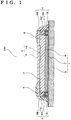
FIG. 1 is a cross-sectional view illustrating the preferred embodiment of the photoelectric conversion device in accordance with the present invention.FIG. 2 is a partial enlarged view ofFIG. 1 . Aphotoelectric conversion device 100 shown inFIG. 1 is a dye-sensitized solar cell. - As shown in
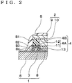
FIG. 1 , thephotoelectric conversion device 100 is provided with a workingelectrode 1 and a counter electrode (second electrode) 2 disposed so as to be opposite the workingelectrode 1. The workingelectrode 1 supports a photosensitizing dye. Anelectrolytic solution 3 is disposed between the workingelectrode 1 and thecounter electrode 2, and a sealingportion 4 is provided between the workingelectrode 1 and thecounter electrode 2 around theelectrolytic solution 3. As shown inFIG. 2 , in the sealingportion 4, asecond resin 5 is provided so as to cover at least a boundary B1 of the sealingportion 4 and thecounter electrode 2 and a boundary B4 of the sealingportion 4 and the workingelectrode 1. - The working
electrode 1 is provided with a transparent electrode (first electrode) composed of atransparent substrate 6 and a transparentconductive layer 7 provided on the side of thetransparent substrate 6 that faces thecounter electrode 2 and asemiconductor portion 8 serving as one photoelectric conversion portion provided on the transparentconductive layer 7. The photosensitizing dye is supported on thesemiconductor portion 8. Thesemiconductor portion 8 is in contact with the electrolytic solution. - The material constituting the
transparent substrate 6 may be a transparent material. Examples of such transparent material include glass, polyethylene terephthalate (PET), polyethylene naphthalate (PEN), polycarbonates (PC), and polyethersulfones (PES). - Examples of the material constituting the transparent
conductive layer 7 include conductive metal oxides such as tin-doped indium oxide (Indium-Tin-Oxide: ITO), tin oxide (SnO2), fluorine-doped tin oxide (FTO). The transparentconductive layer 7 may be constituted by a single layer or by a laminated body of a plurality of layers constituted by different conductive metal oxides. When thetransparent layer 7 is constituted by a single layer, it is preferred that the transparentconductive layer 7 be constituted by FTO since such a layer has high heat resistance and chemical resistance. When a laminated body constituted by a plurality of layers is used for the transparentconductive layer 7, it is preferred that the laminated body be capable of reflecting the properties of each layer. Above all, it is preferred that a laminated body including a layer constituted by ITO and a layer constituted by FTO be used. In this case, the transparentconductive layer 7 having high conductivity, heat resistance, and chemical resistance can be realized. The thickness of the transparentconductive layer 7 may be for example within a range of 0.01 µm to 2 µm. - The
semiconductor portion 8 has one semiconductor layer constituted by a porous oxide semiconductor film. The porous oxide semiconductor film constituting the semiconductor layer is constituted, for example, by oxide semiconductor particles which are constituted by titanium oxide (TiO2), zinc oxide (ZnO), tungsten oxide (WO3), niobium oxide (Nb2O5), strontium titanate (SrTiO3), tin oxide (SnO2), indium oxide (In3O3), zirconium oxide (ZrO2), thallium oxide (Ta2O5), lanthanum oxide (La2O3), yttrium oxide (Y2O3), holmium oxide (Ho2O3), bismuth oxide (Bi2O3), cerium oxide (CeO2), aluminum oxide (Al2O3), or combinations of two or more thereof. It is preferred that the average particle size of these oxide semiconductor particles be 1 nm to 1000 nm, since the surface area of the oxide semiconductor covered with a dye is increased, that is, a field performing photoelectric conversion is expanded and a larger number of electrons can be generated. In this case, the semiconductor layer is preferably constituted by piling up oxide semiconductor particles of different particle size distributions. In this case, light reflection can be repeatedly induced inside the semiconductor layer, and light can be efficiently converted into electrons, without loss of the incident light to the outside of the semiconductor layer. The thickness of thesemiconductor portion 8 may be, for example, 0.5 µm to 50 µm. Thesemiconductor portion 8 can be also constituted by a laminated body of a plurality of semiconductor layers composed of different materials. - Ruthenium complexes having a ligand including a bipyridine structure or terpyridine structure, or organic dyes such as porphyrin, eosin, rhodamine, and merocyanine can be used as the photosensitizing dye.
- The
counter electrode 2 is provided with aconductive layer 9 and acatalyst layer 10 that is provided on the side of theconductive layer 9 facing the workingelectrode 1 and enhances the reduction reaction at the surface of thecounter electrode 2. - The
conductive layer 9 is constituted by a corrosion-resistant metal material such as titanium, nickel, platinum, molybdenum, and tungsten, a conductive oxide such as ITO and FTO, carbon, or conductive polymers. - The
catalyst layer 10 is constituted by platinum, carbon-based material, and conductive polymers. - The
electrolytic solution 3 includes, for example, a redox pair such as I-/I3 - and an organic solvent. Examples of organic solvents include: acetonitrile, methoxyacetonitrile, propionitrile, ethylene carbonate, propylene carbonate, diethyl carbonate, and γ-butyrolactone. The redox pair may be, for example, a pair such as a bromine/bromide ion in addition to I-/I3 -.. - Examples of the
electrolytic solution 3 include an electrolytic solution obtained by dissolving a predetermined amount of 1-methyl-3-methylimidazolium iodide, LiI, I2, and 4-t-butylpyridine in ionic liquid electrolyte, for example, 1-ethyl-3-methylimidazolium bis(trifluoromethylsulfonyl)imide. Further, a nanocomposite ion gel electrolyte, which is a pseudo-solid electrolyte in a gel form obtained by mixing nanoparticles such as SiO2, TiO2, and carbon nanotubes with the ionic liquid electrolyte, may be also used as theelectrolytic solution 3. An ionic liquid electrolyte can be also gelled by using an organic gelling agent such as polyvinylidene fluoride, a polyethylene oxide derivative or an amino acid derivative. - The sealing
portion 4 links the workingelectrode 1 and thecounter electrode 2 and includes awiring portion 4A serving as an inorganic sealing portion that is fixed on the surface of the workingelectrode 1 that faces thecounter electrode 2 and aresin sealing portion 4B linking thewiring portion 4A and thecounter electrode 2. Thewiring portion 4A andresin sealing portion 4B are arranged in a row along the direction connecting the workingelectrode 1 and thecounter electrode 2. Thus, thewiring portion 4A and theresin sealing portion 4B are arranged in a row along the direction from the workingelectrode 1 to thecounter electrode 2. - In the present embodiment, the
wiring portion 4A is provided so as to be on the surface of the transparentconductive layer 7 and enclose thesemiconductor portion 8. In the present embodiment, the current-collectingwiring 11 is present inside thewiring portion 4A, the entire current-collectingwiring 11 is covered by a wiringprotective layer 12, and contact between theelectrolytic solution 3 and the current-collectingwiring 11 is prevented. Thus, thewiring protection layer 12 is provided so as to straddle the current-collectingwiring 11. In other words, in thephotoelectric conversion device 100 of the present embodiment, thewiring portion 4A is effectively used as an inorganic sealing portion. Thewiring protection layer 12 may or may not be in contact with the transparentconductive layer 7 of the workingelectrode 1, as long as the wiring protection layer covers the entire current-collectingwiring 11. - The material constituting the current-collecting
wiring 11 may be a material having an electric resistance lower than that of the transparentconductive layer 7. Examples of such material include metals such as gold, silver, copper, platinum, aluminum, titanium, and nickel. - Examples of the material constituting the
wiring protection layer 12 include inorganic insulating materials such as a lead-free transparent low-melting-point glass frit. - It is preferred that the
wiring protection layer 12 be covered with athird resin 13 having chemical resistance so as to prevent the contact between theelectrolytic solution 3 and the current-collectingwiring 11 over a longer period and also prevent the appearance of dissolved components of thewiring protection layer 12 in the case in which theelectrolytic solution 3 has come into contact with thewiring protection layer 12. - Examples of the third resin include polyimides, fluororesins, resins cured by ultraviolet ray and also an acid-modified polyethylene, polyvinyl alcohol and an ethylene-vinyl alcohol copolymer. The acid-modified polyethylene means a compound obtained by random copolymerization, alternate copolymerization, block copolymerization, or graft copolymerization of polyethylene with an acid or compounds obtained by neutralization thereof with metal ions. For example, an ethylene-methacrylic acid copolymer is obtained by copolymerization of ethylene and methacrylic acid and is an acid-modified polyethylene. An ionomer obtained by neutralization of an ethylene-methacrylic acid copolymer with metal ions is also an acid-modified polyethylene.
- The
resin sealing portion 4B may be constituted by a material including a first resin. The resin sealing portion is also called a resin portion. The first resin may be any resin if it is a resin, but it is preferred that the first resin be an acid-modified polyethylene or a resin cured by ultraviolet ray. When an acid-modified polyethylene or a resin cured by ultraviolet ray is used as the first resin, the adhesion between the transparent electrode of the workingelectrode 1,counter electrode 2, orwiring portion 4A and the first resin is strong, and the leak of theelectrolytic solution 3 at the interfaces thereof can be inhibited. Further, the first resin may also be polyvinyl alcohol or an ethylene-vinyl alcohol copolymer. When polyvinyl alcohol or an ethylene-vinyl alcohol copolymer is used as the first resin, since these resins have high gas barrier ability, the leak of theelectrolytic solution 3 in the first resin can be inhibited. - It is more preferred that the first resin be an acid-modified polyethylene. In this case, in addition to the aforementioned reasons, since an acid-modified polyethylene is extremely stable against organic solvents contained in the
electrolytic solution 3, physical properties of the first resin, such as flexibility and adhesive ability, can be maintained over a long period. It is even more preferred that an acid-modified polyethylene be an ethylene-methacrylic acid copolymer, an ionomer, or polyethylene modified by maleic anhydride. In this case, in addition to the above-described reasons, since the polarity of the first resin is high, adhesion to the transparent electrode of the workingelectrode 1,counter electrode 2, orwiring portion 4A becomes even stronger. - The
resin sealing portion 4B may be constituted only by a resin or by a resin and an inorganic filler. - An acid-modified polyethylene or a resin cured by ultraviolet ray is preferred as a
second resin 5. When an acid-modified polyethylene or a resin cured by ultraviolet ray is used as thesecond resin 5, strong adhesion between the transparent electrode of the workingelectrode 1,counter electrode 2,wiring portion 4A, or the first resin and second resin becomes strong, and the leak of theelectrolytic solution 3 at the interfaces thereof can be inhibited. Thesecond resin 5 is preferably polyvinyl alcohol or an ethylene-vinyl alcohol copolymer. When polyvinyl alcohol or an ethylene-vinyl alcohol copolymer is used as thesecond resin 5, since these resins have high gas barrier ability, the leak of theelectrolytic solution 3 in thesecond resin 5 can be inhibited. When the first resin includes at least one species of polyvinyl alcohol and an ethylene-vinyl alcohol copolymer, by ensuring the presence of a very small amount of water on the interface of the first resin and second resin, the two resins dissolve and bond mutually in the vicinity of the interface. Therefore, the leak of theelectrolytic solution 3 is inhibited even more adequately. The abovementioned resins may be used individually as thesecond resin 5 or two or more of these resins may be mixed or laminated. It is preferred that thesecond resin 5 be different from the resin contained in theresin sealing portion 4B or athird resin 13, because this enables optimum selection of the resins according to the functions thereof, for example, strength, ability to inhibit the permeation of the leaking liquid, and heat resistance. - However, when the
second resin 5 is a resin including repeating units identical to the resin contained in theresin sealing portion 4B or athird resin 13, there is an advantage that adhesion at the interfaces is improved since the resins are likely to have similar properties in thermal properties, solubility in solvents, and response to light. For example, if thesecond resin 5 and theresin sealing portion 4B both include at least one species selected from the group consisting of an acid-modified polyethylene and an ethylene-vinyl alcohol copolymer, since these resins include repeating units of unsaturated carbon chains corresponding to ethylene, they can be easily fused by heating and will maintain the original physical properties even after cooling. Therefore, strong bonds can be obtained when bonding interfaces thereof are thermally fused and bonded together. - If the
second resin 5 and theresin sealing portion 4B both include at least one species selected from the group consisting of polyvinyl alcohol and an ethylene-vinyl alcohol copolymer, since both include repeating units of unsaturated carbon chains having hydroxyl groups corresponding to vinyl alcohol, the resins are soluble in water. As a result, by ensuring the presence of a very small amount of water on the bonding interfaces, it is possible to make the resins compatible to each other in the vicinity of the interfaces and strongly bond the resins together. - In the present embodiment, the
second resin 5 covers not only the boundary B1 of the sealingportion 4 and thecounter electrode 2 and the boundary B4 of the sealingportion 4 and the workingelectrode 1, but also the boundary B2 of thethird resin 13 and theresin sealing portion 4B and the boundary B3 of thethird resin 13 and thewiring portion 4A. In this case, thethird resin 13 forms a boundary of thewiring portion 4A and theresin sealing portion 4B, and thethird resin 13 is covered by thesecond resin 5. - The operation and effect of the
photoelectric conversion device 100 will be explained below. - In the above-described
photoelectric conversion device 100, the sealingportion 4 is provided with thewiring portion 4A and theresin sealing portion 4B connecting thewiring portion 4A and thecounter electrode 2, and thewiring portion 4A and theresin sealing portion 4B are arranged in a row along the direction connecting the workingelectrode 1 and thecounter electrode 2. Herein, thewiring portion 4A is constituted by the current-collectingwiring 11 and thewiring protection layer 12, and both the current-collectingwiring 11 and thewiring protection layer 12 are constituted by inorganic materials. By contrast, theresin sealing portion 4B is constituted by a material including the first resin. Therefore, thewiring portion 4A has sealing ability with respect to theelectrolytic solution 3 higher than that of theresin sealing portion 4B. Further, in thephotoelectric conversion device 100, because of the presence of thewiring portion 4A, the ratio of the interface surface of thewiring portion 4A, which has high sealing ability with respect to theelectrolytic solution 3, and theelectrolytic solution 3 in the interface surface of theelectrolytic solution 3 and the sealingportion 4 can be increased by comparison with that in the case in which the sealingportion 4 is constituted only by theresin sealing portion 4B. - Thus, in the case in which the sealing
portion 4 is constituted only by theresin sealing portion 4B, the leak of theelectrolytic solution 3 tends to occur comparatively easily in theresin sealing portion 4B. Therefore, it may be said that the leak cross-sectional area of theelectrolytic solution 3 becomes large in the sealingportion 4. By contrast, since the sealingportion 4 of the present embodiment includes not only theresin sealing portion 4B, but also thewiring portion 4A, the surface area of theresin sealing portion 4 where the leak of theelectrolytic solution 3 occurs comparatively easily, that is, the leak cross-sectional area of theelectrolytic solution 3, is reduced. - As a result, with the
photoelectric conversion device 100, the leak of theelectrolytic solution 3 can be sufficiently inhibited and therefore changes in the photoelectric conversion efficiency with time can be sufficiently inhibited. Therefore, a longer service life of thephotoelectric conversion device 100 can be realized. - In the
photoelectric conversion device 100 of the present embodiment, thesemiconductor portion 8 can be enlarged by disposing the current-collectingwiring 11 inside thewiring portion 4A. More specifically, the surface area of the interface of thesemiconductor portion 8 and the transparentconductive layer 7 can be enlarged. Therefore, a ratio (a ratio of the surface area of the interface of thesemiconductor portion 8 and the transparentconductive layer 7 constituting the workingelectrode 1 to the surface area of the portion surrounded by the sealingportion 4 in the surface of the transparentconductive layer 7 constituting the workingelectrode 1 on the side facing the counter electrode 2) contributing to power generation can be increased and photoelectric conversion efficiency per the workingelectrode 1 can be increased. - In the above-mentioned
photoelectric conversion device 100, the sealingportion 4 is provided with thewiring portion 4A and theresin sealing portion 4B linking thewiring portion 4A and thecounter electrode 2, and thewiring portion 4A and theresin sealing portion 4B are disposed in a row along the direction connecting the transparentconductive layer 7 and thecounter electrode 2. Herein, thewiring portion 4A is constituted by the current-collectingwiring 11 and thewiring protection layer 12, and these current-collectingwiring 11 and thewiring protection layer 12 are both constituted by inorganic materials. By contrast, theresin sealing portion 4B is constituted by a material including a resin. Therefore, theresin sealing portion 4B has stress relaxation ability higher than that of thewiring portion 4A. - Where the sealing
portion 4 is constituted only by thewiring portion 4A composed of the current-collectingwiring 11 and thewiring protection layer 12, when thephotoelectric conversion device 100 is placed under an environment with large temperature variations, stresses can be concentrated in thewiring portion 4A due to a difference in thermal expansion coefficient between the transparent electrode of the workingelectrode 1 and thecounter electrode 2. Due to the stresses, thewiring portion 4A tends to peel off from the transparentconductive layer 7, cracks tend to appear in thewiring portion 4A, and the leak of theelectrolytic solution 3 tends to occur easily. By contrast, since the sealingportion 4 of the present embodiment is provided not only with thewiring portion 4A, but also with theresin sealing portion 4B, when the stresses are applied to the sealingportion 4, the applied stresses are absorbed by theresin sealing portion 4B. - Therefore, with the
photoelectric conversion device 100, even when thephotoelectric conversion device 100 is used under an environment with large temperature variations, the occurrence of peeling and damage such as cracks in thewiring portion 4A can be prevented. Therefore, the leak of theelectrolytic solution 3 caused by the damage of thewiring portion 4A can be prevented and therefore changes in the photoelectric conversion efficiency with time can be sufficiently inhibited. - Further, in the
photoelectric conversion device 100 of the present embodiment, where the current-collectingwiring 11 is disposed on the side of the sealingportion 4 that is opposite the side facing thesemiconductor portion 8, an area to be occupied by the current-collectingwiring 11 is needed on the side of the sealingportion 4 that is opposite the side facing thesemiconductor portion 8. Meanwhile, where the current-collectingwiring 11 is disposed between the sealingportion 4 and thesemiconductor portion 8, thesemiconductor portion 8 cannot be brought sufficiently close to the sealingportion 4 due to the presence of the current-collectingwiring 11 and the surface area of the semiconductor is decreased. - By contrast, with the
photoelectric conversion device 100 of the present embodiment, the current-collectingwiring 11 is provided in the sealingportion 4 neither on the side of the sealingportion 4 that is opposite the side facing thesemiconductor portion 8, nor on the side of the sealingportion 4 that faces thesemiconductor portion 8. Thus, the current-collecting wiring is provided as part of the sealingportion 4 inside the sealingportion 4. Therefore, the surface area occupied by the current-collectingwiring 11 and the sealingportion 4 in the light incidence surface of the workingelectrode 1 can be minimized, and the incident light blocked by the current-collectingwiring 11 and the sealingportion 4 can be minimized. Therefore, the surface area of thesemiconductor portion 8 along the surface of the transparentconductive layer 7 can be enlarged. As a result, according tophotoelectric conversion device 100, it is possible to obtain high photoelectric conversion efficiency. - Further, with the
photoelectric conversion device 100, in the sealingportion 4, thesecond resin 5 is provided so as to cover the boundary B1 of the sealingportion 4 and thecounter electrode 2, the boundary B4 of the sealingportion 4 and the workingelectrode 1, the boundary B2 of thethird resin 13 and theresin sealing portion 4B, and the boundary B3 of thethird resin 13 and thewiring portion 4A. Therefore, the leak of theelectrolytic solution 3 is inhibited not only by theresin sealing portion 4B, but also by thesecond resin 5. In particular, the leak of theelectrolytic solution 3 through the interface of the sealingportion 4 and the workingelectrode 1, the interface of the sealingportion 4 and thecounter electrode 2, the interface of thethird resin 13 and theresin sealing portion 4B, and the interface of thethird resin 13 and thewiring portion 4A can be effectively inhibited by thesecond resin 5. Therefore, changes in photoelectric conversion efficiency with time can be inhibited more sufficiently. - The
photoelectric conversion device 100 of the present embodiment is particularly effective when thecounter electrode 2 is a thin flexible material such as a metal foil. Thus, when thecounter electrode 2 is constituted by a flexible material such as a metal foil, where theresin sealing portion 4B, rather than thewiring portion 4A, is fixed to thecounter electrode 2, theresin sealing portion 4B follows the deformation of thecounter electrode 2 more easily than thewiring portion 4A. As a result, cracks are unlikely to occur in thewiring portion 4A and theresin sealing portion 4B is unlikely to peel off from thecounter electrode 2. - Next, a method for manufacturing the
photoelectric conversion device 100 will be explained below. - First, the working
electrode 1 and thecounter electrode 2 are prepared. - The working
electrode 1 can be obtained by forming the transparentconductive layer 7 on thetransparent substrate 6, then forming thesemiconductor portion 8 on the transparentconductive layer 7, and causing a photosensitizing dye to support on thesemiconductor portion 8. - Examples of methods for forming the transparent
conductive layer 7 on thetransparent substrate 6 include, for example, sputtering, vapor deposition, spray pyrolysis deposition (SPD), and CVD. - The
semiconductor portion 8 is usually constituted by a porous oxide semiconductor film. The porous oxide semiconductor film can be obtained, for example, by sintering the above-described oxide semiconductor particles. - Then, the current-collecting
wiring 11 is formed on at least part of the periphery of thesemiconductor portion 8 in the workingelectrode 1, and then thewiring protection layer 12 is formed so as to cover the current-collectingwiring 11 and also to surround the periphery of thesemiconductor portion 8. Thewiring portion 4A is thus obtained around thesemiconductor portion 8. - The current-collecting
wiring 11 can be obtained, for example, by compounding metal particles constituting the above-described current-collectingwiring 11 with a thickening agent such as polyethylene glycol to obtain a paste, coating the paste by using a screen printing method or the like to surround thesemiconductor portion 8, and calcining by heating. Further, when the workingelectrode 1 is conductive glass, the current-collectingwiring 11 is strongly bonded to the workingelectrode 1 by mixing a low-melting-point glass frit with the above-described paste. - The
wiring protection layer 12 can be obtained, for example, by compounding, if necessary, a thickening agent, a binder, a dispersant, and a solvent with an inorganic insulating material such as the aforementioned low-melting-point glass frit to obtain a paste, coating the paste by screen printing method or the like so as to cover the entire current-collectingwiring 11 and calcining by heating. - In order to prevent the contact of the
electrolytic solution 3 with the current-collectingwiring 11 over a longer period and also to prevent the appearance of dissolved components of thewiring protection layer 12 in the case in which theelectrolytic solution 3 has come into contact with thewiring protection layer 12, it is preferred that thewiring protection layer 12 be covered with thethird resin 13 having chemical resistance, such as a polyimide, a fluororesin, an acid-modified polyethylene, polyvinyl alcohol, an ethylene-vinyl alcohol copolymer, and a resin cured by ultraviolet ray. The sealingportion 4 can be covered with thethird resin 13, for example, in the following matter. When thethird resin 13 is a thermoplastic resin, thethird resin 13 can be obtained by coating the moltenthird resin 13 on thewiring protection layer 12 and then cooling naturally at room temperature, or by bringing a film-likethird resin 13 into contact with thewiring protection layer 12, heating and melting the film-likethird resin 13 by an external heat source, and then cooling naturally at room temperature. For example, an ionomer, an ethylene-methacrylic acid copolymer, or polyethylene modified with maleic anhydride can be used as the thermoplasticthird resin 13. When thethird resin 13 is a resin cured by ultraviolet ray, thethird resin 13 can be obtained by coating the ultraviolet curable resin, which is a precursor of thethird resin 13, on thewiring protection layer 12 and then curing the aforementioned ultraviolet curable resin by ultraviolet ray. When thethird resin 13 is a water-soluble resin, thethird resin 13 can be obtained by coating an aqueous solution including thethird resin 13 on thewiring protection layer 12. For example, vinyl alcohol polymer, and an ethylene-vinyl alcohol copolymer can be used as the water-solublethird resin 13. - In order to cause the photosensitizing dye to support on the
semiconductor portion 8 of the workingelectrode 1, usually, the workingelectrode 1 obtained by forming thesemiconductor portion 8 on the transparentconductive layer 7 is immersed in a solution including the photosensitizing dye, the dye is adsorbed on thesemiconductor portion 8 and then the extra dye is washed out with the solvent component of the abovementioned solution and dried. Thus, the photosensitizing dye is adsorbed on thesemiconductor portion 8. However, it is also possible to cause the photosensitizing dye to support on thesemiconductor portion 8 by coating a solution including the photosensitizing dye on thesemiconductor portion 8 and drying, thereby causing the adsorption of the photosensitizing dye to adsorb on thesemiconductor portion 8 constituted by a porous oxide semiconductor film. - Meanwhile, the
counter electrode 2 can be obtained by forming thecatalyst layer 10 on theconductive layer 9. In thecounter electrode 2, theconductive layer 9 is constituted, for example, by a metal foil composed of the abovementioned metal material, and thecatalyst layer 10 can be formed by sputtering by using platinum or the like. In this case, even if an uneven structure is formed due to a difference in height between thewiring protection layer 12 and thesemiconductor portion 8 measured by taking the surface of the transparentconductive layer 7 of the workingelectrode 1 as a reference level, thecounter electrode 2 can be easily deformed to follow the uneven structure. - Then, the first resin or a precursor thereof for linking the
wiring portion 4A and thecounter electrode 2 is formed on thecounter electrode 2. When the first resin is a thermoplastic resin, the first resin can be obtained by coating the molten first resin on thecounter electrode 2 and then cooling naturally at room temperature, or by bringing a film-like first resin into contact with thecounter electrode 2, heating and melting the film-like first resin by an external heat source, and then cooling naturally at room temperature. For example, an ionomer, an ethylene-methacrylic acid copolymer, or polyethylene modified with maleic anhydride can be used as the thermoplastic first resin. When the first resin is a resin cured by ultraviolet ray, the ultraviolet curable resin, which is a precursor of the first resin, is coated on thecounter electrode 2. When the first resin is a water-soluble resin, an aqueous solution including the first resin is coated on thecounter electrode 2. For example, a vinyl alcohol polymer and an ethylene-vinyl alcohol copolymer can be used as the water-soluble first resin. - The working
electrode 1 and thecounter electrode 2 are disposed opposite each other, the fist resin and thewiring portion 4A are superimposed, and a laminated body is formed. When the first resin is a thermoplastic resin, the first resin is heated and melted and thewiring portion 4A and thecounter electrode 2 are bonded together. As a result, theresin sealing portion 4B linking thewiring portion 4A and thecounter electrode 2 is obtained therebetween. When the first resin is a resin cured by ultraviolet ray, the abovementioned ultraviolet curable resin is cured by ultraviolet ray after the laminated body has been formed, and theresin sealing portion 4B linking thewiring portion 4A and thecounter electrode 2 is obtained therebetween. When the first resin is a water-soluble resin, finger-touch drying is conducted at room temperature after the laminated body has been formed, then drying is performed under low-humidity atmosphere, and theresin sealing portion 4B linking thewiring portion 4A and thecounter electrode 2 is obtained therebetween. - Next, the space surrounded by the working
electrode 1,counter electrode 2, and sealingportion 4 is filled with theelectrolytic solution 3. The space can be filled with theelectrolytic solution 3, for example, by pouring theelectrolytic solution 3 via an electrolytic solution injection port (not shown in the figure) that has been formed in advance in thecounter electrode 2 and finally sealing the electrolytic solution injection port with the abovementioned first resin. - Then, the sealing
portion 4 is then covered with thesecond resin 5. When thesecond resin 5 is a thermoplastic resin, thesecond resin 5 can be obtained by coating the moltensecond resin 5 on the sealingportion 4 and then cooling naturally at room temperature, or bringing a film-likesecond resin 5 into contact with the sealingportion 4, heating and melting the film-likesecond resin 5 by an external heat source, and then cooling naturally at room temperature. For example, an ionomer, an ethylene-methacrylic acid copolymer, or polyethylene modified with maleic anhydride can be used as the thermoplasticsecond resin 5. - When the
second resin 5 is a resin cured by ultraviolet ray, thesecond resin 5 can be obtained by coating the ultraviolet curable resin, which is a precursor of thesecond resin 5, on the sealingportion 4 and then curing the ultraviolet curable resin, which is a precursor of thesecond resin 5, with ultraviolet ray. As a precursor for the resin cured by ultraviolet ray that constitutes thesecond resin 5, 31x-101 (ThreeBond Co.) can be used. - When the
second resin 5 is a water-soluble resin, thesecond resin 5 can be obtained by coating an aqueous solution including thesecond resin 5 on the sealingportion 4 and drying, for example, under the ambient atmosphere at room temperature. For example, vinyl alcohol polymer and an ethylene-vinyl alcohol copolymer can be used as the water-solublesecond resin 5. Regardless of whether thesecond resin 5 is a thermoplastic resin, resin cured by ultraviolet ray, or water-soluble resin, it is preferred that the second resin be provided so as to cover at least the boundary B1 of the sealingportion 4 and thecounter electrode 2, the boundary B4 of the sealingportion 4 and the workingelectrode 1, the boundary B2 of thethird resin 13 and theresin sealing portion 4B, and the boundary B3 of thethird resin 13 and thewiring portion 4A. For this purpose, thesecond resin 5 is coated not only on the sealingportion 4, but also on the peripheral edge of thecounter electrode 2 and a portion outside the sealingportion 4 in the transparentconductive layer 7 constituting the workingelectrode 1. When thesecond resin 5 is a sheet-like thermoplastic resin, the sheet of thesecond resin 5 is also brought into contact with the peripheral edge of thecounter electrode 2 and a portion outside the sealingportion 4 in the transparentconductive layer 7 constituting the workingelectrode 1 and the film-likesecond resin 5 is heated and melted by an external heat source. - Thus, the production of the
photoelectric conversion device 100 is completed. - When the
electrolytic solution 3 is constituted by the above-described nanocomposite ion gel electrolyte, theelectrolytic solution 3 is disposed between the workingelectrode 1 supporting the dye and thecounter electrode 2 in the following matter. Thus, before the workingelectrode 1 supporting the dye and thecounter electrode 2 are disposed opposite each other, the paste including the above-mentioned nanocomposite ion gel electrolyte is coated, for example by a screen printing method, on the inner region of thewiring portion 4A on the workingelectrode 1 supporting the dye. Then, the workingelectrode 1 supporting the dye and thecounter electrode 2 are disposed opposite each other, the first resin and thewiring portion 4A are superimposed, and a laminated body is formed. When the first resin is a thermoplastic resin, the first resin is heated and melted and thewiring portion 4A and thecounter electrode 2 are bonded together. Theresin sealing portion 4B linking thewiring portion 4A and thecounter electrode 2 is thus obtained therebetween. When the first resin is a resin cured by ultraviolet ray, the abovementioned ultraviolet curable resin is cured by ultraviolet ray after the laminated body has been formed, and theresin sealing portion 4B linking thewiring portion 4A and thecounter electrode 2 is obtained therebetween. When the first resin is a water-soluble resin, finger-touch drying is conducted at room temperature after the laminated body has been formed, then drying is performed under low-humidity atmosphere, and theresin sealing portion 4B linking thewiring portion 4A and thecounter electrode 2 is obtained therebetween. Theelectrolytic solution 3 constituted by the above-described nanocomposite ion gel electrolyte can thus be disposed between the workingelectrode 1 and thecounter electrode 2. The sealingportion 4 is then covered with thesecond resin 5 and thephotoelectric conversion device 100 is obtained. - The second embodiment of the photoelectric conversion device in accordance with the present invention will be explained below with reference to
FIGS. 3 and4 . InFIGS. 3 and4 , constituent elements identical or similar to those of the first embodiment will be assigned with same reference numerals and explanation thereof will be herein omitted. -
FIG. 3 is a cross-sectional view of the photoelectric conversion device of the present embodiment.FIG. 4 is a partial enlarged view ofFIG. 3 . As shown inFIG. 3 , thephotoelectric conversion device 200 of the present embodiment is different from thephotoelectric conversion device 100 of the first embodiment in that aninorganic sealing portion 204A is used instead of thewiring portion 4A, thewiring portion 4A is disposed between a sealingportion 204 and thesemiconductor portion 8 on the surface of the transparentconductive layer 7 of the workingelectrode 1, and theinorganic sealing portion 204A is constituted by an inorganic insulating material and does not have the current-collectingwiring 11. Herein, theinorganic sealing portion 204A and theresin sealing portion 4B are disposed in a row along the direction connecting the workingelectrode 1 and thecounter electrode 2, in the same manner as in the first embodiment. - Even in this case, the
inorganic sealing portion 204A also has sealing ability with respect to theelectrolytic solution 3 that is higher than that of theresin sealing portion 4B and therefore variations in photoelectric conversion efficiency with time can be sufficiently inhibited. Further, theinorganic sealing portion 204A is not restricted by the current-collectingwiring 11. Therefore, as shown inFIG. 4 , it is possible to make a width W1 of theinorganic sealing portion 204A narrower than a width W2 of the wiring portion (current-collecting portion) 4A constituted by the current-collectingwiring 11 and thewiring protection layer 12. As a result, the light-receiving surface area of thephotoelectric conversion device 200, that is, the aperture ratio, can be further increased. Herein, the width means a width along the surface of the transparentconductive layer 7 on the side facing thecounter electrode 2. Further, in thephotoelectric conversion device 200 of the present embodiment, the current-collectingwiring 11 is disposed on the inside of the sealingportion 4. - The
inorganic sealing portion 204A is constituted by an inorganic material. For example, an inorganic insulating material similar to that of thewiring protection layer 12 can be used as the aforementioned inorganic material. - The
inorganic sealing portion 204A can be formed on the workingelectrode 1 for example by a method similar to that used to form thewiring protection layer 12. - The present embodiment is especially effective when the
counter electrode 2 is a thin flexible material such as a metal foil. Thus, when thecounter electrode 2 is constituted by a flexible material such as a metal foil, where theresin sealing portion 4B, rather than theinorganic sealing portion 204A, is fixed to thecounter electrode 2, theresin sealing portion 4B follows the deformation of thecounter electrode 2 more easily than theinorganic sealing portion 204A. As a result, cracks are unlikely to occur in theinorganic sealing portion 204A and theresin sealing portion 4B is unlikely to peel off from thecounter electrode 2. - Further, in the present embodiment, the
third resin 13 covering thewiring protection layer 12 is omitted, but from the standpoint of preventing reliably the contact of the current-collectingwiring 11 and theelectrolytic solution 3 and preventing the appearance of dissolved components of thewiring protection layer 12 caused by theelectrolytic solution 3, it is preferred that thewiring protection layer 12 be covered by thethird resin 13. - The third embodiment of the photoelectric conversion device in accordance with the present invention will be explained below with reference to
FIG. 5 . InFIG. 5 , constituent elements identical or similar to those of the first and second embodiments will be assigned with same reference numerals and explanation thereof will be herein omitted. -
FIG. 5 is a cross-sectional view of the photoelectric conversion device of the present embodiment. As shown inFIG. 5 , thephotoelectric conversion device 300 of the present embodiment is different from thephotoelectric conversion device 200 of the second embodiment in that the current-collectingwiring 11 is disposed on the side of the sealingportion 204 opposite that facing thesemiconductor portion 8. - Even in this case, the
inorganic sealing portion 204A also has sealing ability with respect to theelectrolytic solution 3 that is higher than that of theresin sealing portion 4B and therefore variations in photoelectric conversion efficiency with time can be sufficiently inhibited. Further, theinorganic sealing portion 204A is not restricted by the current-collectingwiring 11. Therefore, it is possible to make the width of theinorganic sealing portion 204A narrower than the width of the current-collecting portion constituted by the current-collectingwiring 11 and thewiring protection layer 12. As a result, the light-receiving surface area of thephotoelectric conversion device 300, that is, the aperture ratio, can be further increased. Herein, the width means a width along the surface of the transparentconductive layer 7 on the side facing thecounter electrode 2. Further, in thephotoelectric conversion device 300 of the present embodiment, the current-collectingwiring 11 is disposed on the side of the sealingportion 4 opposite that facing thesemiconductor portion 8. Therefore, the current-collectingwiring 11 does not come into contact with theelectrolytic solution 3. As a result, it is not necessary to protect the current-collectingwiring 11 and thewiring protection layer 12 and thethird resin 13 become unnecessary. - In the present embodiment, it is similar to the second embodiment that the photoelectric conversion device is particularly effective when the
counter electrode 2 is a thin flexible material such as a metal foil. - Next, the fourth embodiment of the photoelectric conversion device in accordance with the present invention will be explained below with reference to
FIG. 6 . InFIG. 6 , constituent elements identical or similar to those of the first and second embodiments will be assigned with same reference numerals and explanation thereof will be herein omitted. -
FIG. 6 is a cross-sectional view of the photoelectric conversion device of the present embodiment. As shown inFIG. 6 , thephotoelectric conversion device 400 of the present embodiment is different from thephotoelectric conversion device 200 of the second embodiment in that the arrangement of theinorganic sealing portion 204A and theresin sealing portion 4B constituting a sealingportion 404 is reversed. Thus, in thephotoelectric conversion device 400, theinorganic sealing portion 204A is brought into contact with and fixed to thecounter electrode 2, and theresin sealing portion 4B is brought into contact with and fixed to the transparentconductive layer 7 of the workingelectrode 1. Herein, theinorganic sealing portion 204A and theresin sealing portion 4B are disposed in a row along the direction connecting the workingelectrode 1 and thecounter electrode 2, in the same manner as in the second embodiment. - Even in this case, the
inorganic sealing portion 204A also has sealing ability with respect to theelectrolytic solution 3 that is higher than that of theresin sealing portion 4B and therefore variations in photoelectric conversion efficiency with time can be sufficiently inhibited. Further, theinorganic sealing portion 204A is not restricted by the current-collectingwiring 11. Therefore, it is possible to make the width of theinorganic sealing portion 204A narrower than the width of the wiring portion (current-collecting portion) 4A constituted by the current-collectingwiring 11 and thewiring protection layer 12. As a result, the light-receiving surface area, that is, the aperture ratio, can be further increased. - The
photoelectric conversion 400 of the present embodiment is particularly effective when the workingelectrode 1 is a flexible material such as a resin provided with a transparent conductive film, that is, when thetransparent substrate 6 is constituted by a resin in the workingelectrode 1. Thus, when the workingelectrode 1 is constituted by a flexible material such as a resin provided with a transparent conductive film, where theresin sealing portion 4B, rather than theinorganic sealing portion 204A, is fixed to the workingelectrode 1, theresin sealing portion 4B follows the deformation of the workingelectrode 1 more easily than theinorganic sealing portion 204A. As a result, theresin sealing portion 4B is unlikely to peel off from the workingelectrode 1. - In the case in which the first resin constituting the
resin sealing portion 4B is constituted by a resin cured by ultraviolet ray, when irradiation with ultraviolet ray is performed from the workingelectrode 1 side in the process of manufacturing thephotoelectric conversion device 400, it is possible to irradiate a ultraviolet curable resin which is a precursor of the first resin with a ultraviolet ray without being hindered by the current-collectingwiring 11. Therefore, the sealing ability of theresin sealing portion 4B can be improved. - Next, the fifth embodiment of the photoelectric conversion device in accordance with the present invention will be explained below with reference to
FIG. 7 . InFIG. 7 , constituent elements identical or similar to those of the first and second embodiments will be assigned with same reference numerals and explanation thereof will be herein omitted. -
FIG. 7 is a cross-sectional view of the photoelectric conversion device of the present embodiment. As shown inFIG. 7 , thephotoelectric conversion device 500 of the present embodiment is different from thephotoelectric conversion device 200 of the second embodiment in that a sealingportion 504 is further provided with theresin sealing portion 4B, which links theinorganic sealing portion 204A and thecatalyst layer 10 of thecounter electrode 2, between thecounter electrode 2 and theinorganic sealing portion 204A. Herein, theresin sealing portion 4B,inorganic sealing portion 204A, andresin sealing portion 4B are disposed in a row along the direction connecting the workingelectrode 1 and thecounter electrode 2, and the resin sealing portion and the inorganic sealing portion are disposed alternately. - Even in this case, the sealing ability of the of the
inorganic sealing portion 204A with respect to theelectrolytic solution 3 is also higher than that of theresin sealing portion 4B. Therefore, variations in photoelectric conversion efficiency with time can be sufficiently inhibited. - The sealing
portion 504 can be obtained, for example, in the following manner. Thus, the first resin or a precursor thereof is formed around the wiring portion (current-collecting portion) 4A constituted by the current-collectingwiring 11 and thewiring protection layer 12 in the workingelectrode 1. When the first resin is a thermoplastic resin, the first resin can be formed by coating the molten first resin on the transparentconductive layer 7 of the workingelectrode 1 and then cooling naturally at room temperature, or by bringing a film-like first resin into contact with the transparentconductive layer 7 of the workingelectrode 1, heating and melting the film-like first resin by an external heat source, and then cooling naturally at room temperature. When the first resin is a resin cured by ultraviolet ray, the ultraviolet curable resin, which is a precursor of the first resin, is coated on the transparentconductive layer 7 of the workingelectrode 1 to form the precursor of the first resin. When the first resin is a water-soluble resin, the first resin is formed by coating an aqueous solution including the first resin on the transparentconductive layer 7 of the workingelectrode 1. Theinorganic sealing portion 204A is then placed on the first resin formed in the above-described manner. Next, when the first resin is a thermoplastic resin, the first resin is heated and melted and theinorganic sealing portion 204A and the workingelectrode 1 are bonded together. Theresin sealing portion 4B linking theinorganic sealing portion 204A and the workingelectrode 1 is thus obtained therebetween. When the first resin is a resin cured by ultraviolet ray, after a laminated body is formed, that is, after theinorganic sealing portion 204A is placed on the first resin, the above-mentioned ultraviolet curable resin is cured by ultraviolet ray and theresin sealing portion 4B linking theinorganic sealing portion 204A and the workingelectrode 1 is obtained therebetween. When the first resin is a water-soluble resin, after a laminated body is formed, that is, after theinorganic sealing portion 204A is placed on the first resin, finger-touch drying is conducted at room temperature, then drying is performed under low-humidity atmosphere, and theresin sealing portion 4B linking theinorganic sealing portion 204A and the workingelectrode 1 is obtained therebetween. - Meanwhile, the first resin or a precursor thereof is formed on the
catalyst layer 10 of thecounter electrode 2. The first resin or a precursor thereof can be formed similarly to theresin sealing portion 4B formed on the transparentconductive layer 7 of the workingelectrode 1. The workingelectrode 1 and thecounter electrode 2 are then disposed opposite each other, the first resin and theinorganic sealing portion 204A are superimposed, and theinorganic sealing portion 204A and thecounter electrode 2 are then bonded together in the same manner as in the case in which theresin sealing portion 4B formed on the transparentconductive layer 7 of the workingelectrode 1 and theinorganic sealing portion 204A are bonded together. As a result, theresin sealing portion 4B is obtained. The sealingportion 504 is thus obtained. - The sixth embodiment of the photoelectric conversion device in accordance with the present invention will be explained below with reference to
FIG. 8 . InFIG. 8 , constituent elements identical or similar to those of the first and second embodiments will be assigned with same reference numerals and explanation thereof will be herein omitted. -
FIG. 8 is a cross-sectional view of the photoelectric conversion device of the present embodiment. As shown inFIG. 8 , thephotoelectric conversion device 600 of the present embodiment is different from thephotoelectric conversion device 100 of the first embodiment in that a sealingportion 604 further includes theinorganic portion 204A between thecounter electrode 2 and theresin sealing portion 4B. Herein, thewiring portion 4A,resin sealing portion 4B, andinorganic sealing portion 204A, are disposed in a row along the direction connecting the workingelectrode 1 and thecounter electrode 2, and the inorganic sealing portion and the resin sealing portion are disposed alternately. - Even in this case, the sealing ability of the
wiring portion 4A and theinorganic sealing portion 204A with respect to theelectrolytic solution 3 is also higher than that of theresin sealing portion 4B. Therefore, variations in photoelectric conversion efficiency with time can be sufficiently inhibited. - The sealing
portion 604 can be obtained, for example, in the following manner. Thus, thewiring portion 4A is formed in the same manner as in the first embodiment on the transparentconductive layer 7 of the workingelectrode 1 and the first resin is formed on thewiring protection layer 12. The formation of the first resin may be performed in the same manner as in the case in which the first resin is formed on the transparentconductive layer 7 of the workingelectrode 1 in the fifth embodiment. - Meanwhile, the
inorganic sealing portion 204A is formed on thecatalyst layer 10 of thecounter electrode 2. The formation method thereof may be performed in the same manner as that in the case in which theinorganic sealing portion 204A is formed on the workingelectrode 1 in the second embodiment. - The working
electrode 1 and thecounter electrode 2 are then disposed opposite each other, the first resin and theinorganic sealing portion 204A are superimposed, and theinorganic sealing portion 204A and thecounter electrode 2 are then bonded together in the same manner as in the case in which the first resin and theinorganic sealing portion 204A are bonded together in the fifth embodiment. As a result, theresin sealing portion 4B is obtained. The sealingportion 604 is thus obtained. - Next, the seventh embodiment of the photoelectric conversion device in accordance with the present invention will be explained below with reference to
FIG. 9 . InFIG. 9 , constituent elements identical or similar to those of the first and sixth embodiments will be assigned with same reference numerals and explanation thereof will be herein omitted. -
FIG. 9 is a cross-sectional view of the photoelectric conversion device of the present embodiment. As shown inFIG. 9 , thephotoelectric conversion device 700 of the present embodiment is different from thephotoelectric conversion device 100 of the first embodiment in that thecounter electrode 702 has atransparent substrate 706 and a transparentconductive layer 707 provided on the side of thetransparent substrate 706 facing the workingelectrode 1 and in that a sealingportion 704 is further provided with asecond wiring portion 704A between acounter electrode 702 and theresin sealing portion 4B. In the present embodiment, both the workingelectrode 1 and thecounter electrode 702 are transparent electrodes. Herein, thewiring portion 4A,resin sealing portion 4B, andsecond wiring portion 704A are disposed in a row along the direction connecting the workingelectrode 1 and thecounter electrode 702, and theresin sealing portion 4B links thewiring portion 4A and thesecond wiring portion 704A. - The
second wiring portion 704A is provided on the surface of the transparentconductive layer 707 and provided so as to surround thesemiconductor portion 8, when viewed from the side facing thecounter electrode 702. Thesecond wiring portion 704A has a second current-collectingwiring 711 and a secondwiring protection layer 712. The second current-collectingwiring 711 is present inside thewiring portion 704A. The second current-collectingwiring 711 is entirely covered by the secondwiring protection layer 712 and prevents the contact of theelectrolytic solution 3 with the second current-collectingwiring 711. Thus, the secondwiring protection layer 712 is provided to straddle the second current-collectingwiring 711. The secondwiring protection layer 712 may or may not be in contact with the transparentconductive layer 707, as long as the second wiring protection layer covers the entire second current-collectingwiring 711. - In such
photoelectric conversion device 700, the workingelectrode 1 and thecounter electrode 702 are transparent electrodes. Therefore, thesemiconductor portion 8 can receive light both at the side facing the workingelectrode 1 and at the side facing thecounter electrode 702 and the photoelectric conversion efficiency can be further increased. Further, since the second current-collectingwiring 711 is disposed as part of the sealingportion 704 inside the sealingportion 704, the incident light blocked by the second current-collectingwiring 711 and the sealingportion 704 can be minimized even on the light incidence surface of thecounter electrode 702 and the photoelectric conversion efficiency can be further increased. - The
transparent substrate 706 of thecounter electrode 702 can be constituted, for example, from a transparent material similar to that of thetransparent substrate 6. The transparentconductive layer 707 can be constituted, for example, by a material similar to that of the transparentconductive layer 7. - The material constituting the current-collecting
wiring 711 is similar to the material constituting the current-collectingwiring 11. The material constituting thewiring protection layer 712 is similar to the material constituting thewiring protection layer 12. - The transparent
conductive layer 707 may be provided on thetransparent substrate 706 similarly to the case in which the transparentconductive layer 7 is formed on thetransparent substrate 6 in the first embodiment. - The sealing
portion 704 can be obtained, for example, in the following manner. Thus, the current-collectingwiring 11 and thewiring protection layer 12 are formed on the transparentconductive layer 7 of the workingelectrode 1 in the same manner as in the first embodiment, and the first resin is formed on thewiring protection layer 12 in the same manner as in the second embodiment. - Meanwhile, the
second wiring portion 704A is formed on the transparentconductive layer 707 of thecounter electrode 702. Thesecond wiring portion 704A may be formed in the same manner in which thewiring portion 4A is formed on the transparentconductive layer 7 in the first embodiment. In this case, it is also preferred that the secondwiring protection layer 712 be covered by athird resin 713 constituted by a material similar to that of thethird resin 13. The secondwiring protection layer 712 may be covered with thethird resin 713 in the same manner as the case in which thewiring protection layer 12 is covered with thethird resin 13. - The working
electrode 1 and thecounter electrode 702 are then disposed opposite each other, the first resin and thesecond wiring portion 704A are superimposed, and the first resin and thesecond wiring portion 704A are bonded together in the same manner as the case in which the first resin and theinorganic sealing portion 204A are bonded together in the second embodiment. As a result, theresin sealing portion 4B is obtained. The sealingportion 704 is thus obtained. - Next, the eighth embodiment of the photoelectric conversion device in accordance with the present invention will be explained below with reference to
FIG. 10 . InFIG. 10 , constituent elements identical or similar to those of the first embodiment will be assigned with same reference numerals and explanation thereof will be herein omitted. -
FIG. 10 is a cross-sectional view of the photoelectric conversion device of the present embodiment. As shown inFIG. 10 , thephotoelectric conversion device 800 of the present embodiment is provided with acounter electrode 801, which is a transparent electrode, and a workingelectrode 802 disposed so as to face thecounter electrode 801. The workingelectrode 802 supports a photosensitizing dye. Theelectrolytic solution 3 is disposed between thecounter electrode 801 and the workingelectrode 802, and a sealingportion 804 is provided between thecounter electrode 801 and the workingelectrode 802 around theelectrolytic solution 3. - The
counter electrode 801 is provided with thetransparent substrate 6 and the transparentconductive layer 7 provided on the side of thetransparent substrate 6 that faces the workingelectrode 802. - The working
electrode 802 is provided with theconductive layer 9 and asemiconductor portion 808 as a photoelectric conversion portion provided on theconductive layer 9. The photosensitizing dye is supported on thesemiconductor portion 808. Thesemiconductor portion 808 has a semiconductor layer configured in the same manner as thesemiconductor portion 8 in the first embodiment and is in contact with theelectrolytic solution 3. - The sealing
portion 804 links thecounter electrode 801 and the workingelectrode 802 and is provided with thewiring portion 4A fixed on the surface of thecounter electrode 801 on the side facing the workingelectrode 802 and theresin sealing portion 4B linking thewiring portion 4A and the workingelectrode 802. Thewiring portion 4A and theresin sealing portion 4B are arranged in a row along the direction from thecounter electrode 801 to the workingelectrode 802. - The
photoelectric conversion device 800 can be manufactured in the following manner. - First, the
counter electrode 801 and the workingelectrode 802 are prepared. - The
counter electrode 801 can be obtained by forming the transparentconductive layer 7 on thetransparent substrate 6. - Then, the
wiring portion 4A is provided on thecounter electrode 801. Thewiring portion 4A may be formed in the same manner as the case in which thewiring portion 4A is formed on the workingelectrode 1 in the first embodiment. - Meanwhile, in the working
electrode 802, thesemiconductor portion 808 is formed on theconductive layer 9. Thesemiconductor portion 808 may be formed in the same manner as the case in which thesemiconductor portion 8 is formed on the transparentconductive layer 7 in the first embodiment. - The photosensitizing dye is then supported on the
semiconductor portion 808 of the workingelectrode 802. The photosensitizing dye may be supported in the same manner as the case in which the photosensitizing dye is supported on thesemiconductor portion 8 in the first embodiment. - Then, the first resin or a precursor thereof for linking the
wiring portion 4A and the workingelectrode 802 is formed on the workingelectrode 802. The first resin or a precursor thereof may be formed in the same manner as the case in which the first resin or a precursor thereof is formed on thecounter electrode 2 in the first embodiment. - The
counter electrode 801 and the workingelectrode 802 are then disposed opposite each other, the first resin and thewiring portion 4A are superimposed to form a laminated body, and theresin sealing portion 4B linking thewiring portion 4A and the workingelectrode 802 is formed therebetween. Theresin sealing portion 4B may be formed in the same manner in which theresin sealing portion 4B is formed in the first embodiment. - Then, the space surrounded by the
counter electrode 801, workingelectrode 802, and sealingportion 804 is filled with theelectrolytic solution 3. Filling with theelectrolytic solution 3 may be performed in the same manner as the case in which the space is filled with theelectrolytic solution 3 in the first embodiment. - The subsequent operations are similar to those of the first embodiment. The production of the
photoelectric conversion device 800 is thus completed. - The present invention is not limited to the above-described embodiments. For example, only one
semiconductor portion 8 orsemiconductor portion 808 is used in the above-described first to eighth embodiments, but a plurality ofsemiconductor portions 8 orsemiconductor portions 808 may be also used. In this case, the current-collectingwiring 11 has, for example, a grid-like or a comb-like shape. In the first, second, and fourth to eighth embodiments, the current-collectingwiring 11 is covered by awiring protection layer 12. In the first and sixth embodiments, the portion of the wiring portion (constituted by the current-collectingwiring 11 and the wiring protection layer 12) that encloses theentire semiconductor portion 8 is the inorganic sealing portion as referred to in the present invention. In the second and third embodiments, theinorganic sealing portion 204A is provided so as to enclose theentire semiconductor portion 8. - In the second to fifth embodiments, the
third resin 13 is not introduced between theinorganic sealing portion 204A and theresin sealing portion 4B, but thethird resin 13 may be introduced between theinorganic sealing portion 204A and theresin sealing portion 4B so as to cover theinorganic sealing portion 204A in order to prevent the contact between theinorganic sealing portion 204A and theelectrolytic solution 3 and the appearance of dissolved components of theinorganic sealing portion 204A caused by theelectrolytic solution 3. - In the above-described embodiments, the
inorganic sealing portion 204A is constituted by the inorganic insulating material, but theinorganic sealing portion 204A is not necessarily limited to the inorganic insulating material and may be constituted by a conductive oxide such as ITO and FTO or an inorganic conductive material such as a metal material, for example Ti, that is not corroded by theelectrolytic solution 3. - Further, in the first to eighth embodiments, the sealing portion comprises two or less inorganic sealing portions and two or less resin sealing portions, but the sealing portion may comprise three or more inorganic sealing portions and three or more resin sealing portions.
- Further, in the second and third embodiments, the
wiring portion 4A can be omitted, as shown inFIG. 11 . Thewiring portion 4A can be also omitted in the fourth and fifth embodiments although such configurations are not shown in the figures. - It goes without saying that the position of the current-collecting
wiring 11 is not limited to those in the first to eighth embodiments and may be different therefrom. - Further, in the first embodiment, the
wiring portion 4A and theresin sealing portion 4B are arranged in a row along the direction connecting the workingelectrode 1 and thecounter electrode 2, but the wiring portion and sealing portion may be also disposed in two rows. Thus, another sealing portion (will be referred to hereinbelow as an "external sealing portion") may be further provided outside the sealingportion 4 and between the workingelectrode 1 and thecounter electrode 2 so as to enclose the sealingportion 4. In this case, the sealing capability and adhesive bonding capability can be further improved. The external sealing portion is also provided with an inorganic sealing portion and a resin sealing portion, and the inorganic sealing portion and resin sealing portion are disposed in a row along the direction connecting the workingelectrode 1 and thecounter electrode 2. In this case, it is preferred that the inorganic sealing portion in the external sealing portion be fixed to thecounter electrode 2 and that the resin sealing portion be fixed to the workingelectrode 1 side. It is further preferred that the inorganic sealing portion of the external sealing portion be fixed to theresin sealing portion 4B of the sealingportion 4 and that the resin sealing portion of the external sealing portion be fixed to thewiring portion 4A of the sealingportion 4. In this case, sealing capability and adhesive bonding capability can be greatly improved and the mechanical strength of the photoelectric conversion device can be also improved. - Further, in the first and sixth to eighth embodiments, the
wiring portion 4A having the current-collectingwiring 11 and thewiring protection layer 12 is provided so as to enclose thesemiconductor portion 8, but thewiring portion 4A may be provided along the sealingportion 4 in part of the sealingportion 4. In this case, the sealingportion 4 is constituted by a first portion where thewiring portion 4A having the current-collectingwiring 11 is present and a second portion where the current-collectingwiring 11 is not present (that is, where thewiring portion 4A is not present). Herein, in the second portion of the sealingportion 4 where thewiring portion 4A is not present, the inorganic sealing portion composed of an inorganic material and having no current-collectingwiring 11 and theresin sealing portion 4B may be configured to be disposed in a row along the direction connecting the workingelectrode 1 and thecounter electrode 2. In this case, the inorganic sealing portion may be constituted, for example, only by thewiring protection layer 12. Herein, thewiring portion 4A and the inorganic sealing portion have sealing ability higher than that of theresin sealing portion 4B. Therefore, the cross-section area of thewiring portion 4A through which theelectrolytic solution 3 can leak is reduced in the same manner as the case in which the wiring portion is provided over theentire sealing portion 4. As a result, variations in photoelectric conversion device with time can be sufficiently inhibited. Herein, the width of the second portion is preferably narrower than that of the first portion. In this case, the light-receiving surface area, that is aperture ratio, of the photoelectric conversion device can be further increased. - Alternatively, when the
wiring portion 4A is present only in part of the sealingportion 4, the second portion of the sealingportion 4 where thewiring portion 4A is not present may be constituted only by theresin sealing portion 4B. - Further, in the seventh embodiment, the
second wiring portion 704A having the current-collectingwiring 711 and thewiring protection layer 712 is provided so as to enclose thesemiconductor portion 8, as viewed from thecounter electrode 702 side, but thewiring portion 704A may be also provided inside the sealingportion 704 along the sealingportion 4 in part of the sealingportion 4. - Further, in the eighth embodiment, the sealing
portion 804 includes thewiring portion 4A and theresin sealing portion 4B, and thecounter electrode 801 and the workingelectrode 802 are linked by thewiring portion 4A and theresin sealing portion 4B, but an inorganic sealing portion may be provided between theresin sealing portion 4B and the workingelectrode 802 and theresin sealing portion 4B nay link thewiring portion 804 and the inorganic sealing portion. - Further, in the first, sixth, and eighth embodiments, the transparent electrode is constituted by the
transparent substrate 6 and the transparentconductive layer 7, and in the seventh embodiment, the transparent electrode is constituted by thetransparent substrate 706 and the transparentconductive layer 707. However, the transparent electrode can be also constituted by conductive glass. In this case, the current-collectingwirings wiring semiconductor portion 8, heating and calcining. In such a way, the current-collectingwirings - In the first to eighth embodiments, the case is explained in which photoelectric conversion device in accordance with the present invention is applied to a dye-sensitized solar cell, but the photoelectric conversion device in accordance with the present invention can be widely applied to photoelectric conversion devices other than the dye-sensitized solar cell, as long as the photoelectric conversion device has a structure using an electrolytic solution and sealing the electrolytic solution with a sealing portion.
- The contents of the present invention will be specifically explained below with reference to examples thereof, but the present invention is not limited to the below-described examples.
- A transparent conductive substrate was prepared in which a transparent conductive layer composed of FTO was formed on a glass substrate that served as a transparent substrate. A paste including titanium oxide nanoparticles was coated by a doctor blade method on the transparent conductive substrate so as to cover the transparent conductive layer and then calcining was conducted for 3 h at 150°C to form a porous oxide semiconductor layer with a thickness of 10 µm on the transparent conductive layer and obtain a working electrode. A N719 dye was then supported on the porous oxide semiconductor layer.
- A conductive layer composed of FTO similar to that used in the fabrication of the transparent conductive layer was also prepared, a thin platinum film composed of platinum was formed by sputtering on the conductive layer, and a counter electrode was obtained. Through holes were formed in two locations in the counter electrode.
- A paste was then prepared by compounding 2 parts by mass of ethyl cellulose, 19 parts by mass of menthanol, and 10 parts by mass of BDGA (diethylene glycol monobutyl ether acetate) with 100 parts by weight of an inorganic insulating material constituted by a low-melting-point glass frit. The paste was coated by a screen printing method on the transparent conductive layer of the working electrode obtained in the above describe manner, so as to enclose the periphery of the porous oxide semiconductor layer, and an inorganic sealing portion was then obtained by heating and calcining for 1 h at 500°C.
- A thermoplastic resin with a width of 2 mm and a thickness of 50 µm that was constituted by Himilan, which is an ionomer, was then formed as the first resin on the thin platinum film of the counter electrode so as to enable superimposition on the inorganic sealing portion.
- The working electrode and counter electrode were then disposed opposite each other, and the first resin and the inorganic sealing portion were superimposed so as to be in contact with each other.
- A resin sealing portion was then obtained by melting the first resin by heating for 60 sec at 150°C, and a sealing portion constituted by the resin sealing portion and inorganic sealing portion was obtained between the working electrode and counter electrode to link these electrodes.
- An electrolytic solution including methoxyacetonitrile as the main solvent, 0.1 M lithium iodide, 0.05 M iodine, and 0.5 M 4-tert-butyl pyridine was then prepared, the electrolytic solution was injected from the two through holes formed in the counter electrode, these through holes were sealed by using a glass plate and a sheet composed of a thermoplastic resin similar to that described hereinabove, and a laminated body subjected to primary sealing was obtained. A photoelectric conversion device composed of the laminated body subjected to primary sealing was thus obtained.
- A photoelectric conversion device was obtained in the same manner as in Example 1, except that Bynel (trade name, manufactured by Du Pont Corp.), which is polyethylene modified with maleic anhydride, was used as the thermoplastic resin constituting the resin sealing portion.
- A photoelectric conversion device was obtained in the same manner as in Example 1, except that Eval (trade name, manufactured by Kuraray Co., Ltd.), which is an ethylene-vinyl alcohol copolymer, was used as the thermoplastic resin constituting the resin sealing portion.
- A photoelectric conversion device was obtained in the same manner as in Example 1, except that a second resin (secondary sealing material) was further formed on the laminated body subjected to primary sealing obtained in Example 1, so as to cover the sealing portion from the outside.
- In this case, the second resin was formed in the following specific manner. Thus, an aqueous solution was prepared by dissolving Poval (trade name, manufactured by Kuraray Co., Ltd.), which is a vinyl alcohol polymer, in pure water. Then, the aqueous solution was coated around the sealing portion so as to cover the boundary of the inorganic sealing portion and the resin sealing portion, the boundary of the inorganic sealing portion and the working electrode, and the boundary of the resin sealing portion and the counter electrode. Water which was the solvent was then naturally dried under a dry atmosphere at room temperature and the second resin composed of Poval was formed.
- A photoelectric conversion device was obtained in the same manner as in Example 4, except that Bynel, which is polyethylene modified with maleic anhydride, was used as the first resin constituting the resin sealing portion.
- A photoelectric conversion device was obtained in the same manner as in Example 4, except that Eval, which is an ethylene-vinyl alcohol copolymer, was used as the first resin constituting the resin sealing portion.
- A photoelectric conversion device was obtained in the same manner as in Example 1, except that a second resin (secondary sealing material) was further formed on the laminated body subjected to primary sealing, so as to cover the sealing portion from the outside.
- In this case, the second resin was formed in the following specific manner. Thus, 31x-101 (trade name, manufactured by ThreeBond Co.), which is a UV-curable resin, was prepared. Then, the UV-curable resin was coated around the sealing portion so as to cover the boundary of the inorganic sealing portion and the resin sealing portion, the boundary of the inorganic sealing portion and the working electrode, and the boundary of the resin sealing portion and the counter electrode. The UV-curable resin was then cured by irradiating the UV-curable resin with ultraviolet ray under dry atmosphere at room temperature and the second resin constituted by the UV-cured resin was formed.
- A photoelectric conversion device was obtained in the same manner as in Example 1, except that a second resin (secondary sealing material) was further formed on the laminated body subjected to primary sealing, so as to cover the sealing portion from the outside.
- In this case, the second resin was formed in the following specific manner. Thus, Nucrel (manufactured by Du Pont-Mitsui Polychemicals Co., Ltd.), which is an ethylene-methacrylic acid copolymer, was prepared. Then, the second resin was coated around the sealing portion so as to cover the boundary of the inorganic sealing portion and the resin sealing portion, the boundary of the inorganic sealing portion and the working electrode, and the boundary of the resin sealing portion and the counter electrode. The second resin was then formed by heating, melting and then naturally cooling (at room temperature) the second resin.
- A photoelectric conversion device was obtained in the same manner as in Example 8, except that Nucrel, which is an ethylene-methacrylic acid copolymer, was used as the first resin constituting the resin sealing portion.
- A photoelectric conversion device was obtained in the same manner as in Example 1, except that a second resin (secondary sealing material) was further formed on the laminated body subjected to primary sealing, so as to cover the sealing portion from the outside.
- In this case, the second resin was formed in the following specific manner. Thus, Himilan, which is an ionomer, was prepared. Then, the second resin was coated around the sealing portion so as to cover the boundary of the inorganic sealing portion and the resin sealing portion, the boundary of the inorganic sealing portion and the working electrode, and the boundary of the resin sealing portion and the counter electrode. The second resin was then formed by heating, melting and then naturally cooling the second resin at room temperature.
- A laminated body subjected to primary sealing was obtained in the same manner as in Example 1 except that 31x-101, which is a UV-curable resin serving as a precursor for UV-cured resin, was coated on a thin platinum film of the counter electrode, the counter electrode and working electrode were disposed opposite each other to ensure superimposition on the inorganic sealing portion formed on the working electrode, and the UV-curable resin was cured by irradiating the UV-curable resin with ultraviolet ray. Poval, which is a vinyl alcohol polymer, was formed around the sealing portion in the same manner as in Example 4 on the laminated body subjected to primary sealing obtained in the above-described manner.
- A photoelectric conversion device was obtained in the same manner as in Example 11, except that Nucrel, which is an ethylene-methacrylic acid copolymer, was used as the second resin (secondary sealing material). In this case, Nucrel, which is an ethylene-methacrylic acid copolymer, was formed to cover the sealing portion in the same manner as in Example 8.
- A photoelectric conversion device was obtained in the same manner as in Example 11, except that the UV-cured resin was formed as the second resin (secondary sealing material) on the laminated body subjected to primary sealing. In this case, the UV-cured resin was formed in the same manner as in Example 7.
- A photoelectric conversion device was obtained in the same manner as in Example 11, except that Himilan, which is an ionomer, was formed as the second resin (secondary sealing material) on the laminated body subjected to primary sealing. In this case, Himilan, which is an ionomer, was formed in the same manner as in Example 10.
- A laminated body subjected to primary sealing was obtained in the same manner as in Example 1 except that an aqueous solution obtained by dissolving Poval, which is a vinyl alcohol polymer, in pure water was coated on a thin platinum film of the counter electrode, water that was the solvent was naturally dried under dry atmosphere at room temperature to form the first resin composed of Poval, the counter electrode and working electrode were disposed opposite each other to superimposed the first resin and the inorganic sealing portion formed on the working electrode, and the first resin was finger-touch dried at room temperature and then dried under low-humidity atmosphere to form a resin sealing portion. A photoelectric conversion device was obtained by forming the UV-cured resin around the sealing portion in the same manner as in Example 7 on the laminated body subjected to primary sealing that was obtained in the above-described manner.
- A photoelectric conversion device was obtained in the same manner as in Example 15, except that Himilan, which is an ionomer, was formed as the second resin (secondary sealing material) on the laminated body subjected to primary sealing. In this case, Himilan, which is an ionomer, was formed to cover the sealing portion in the same manner as in Example 10.
- A photoelectric conversion device was obtained in the same manner as in Example 11, except that Nucrel, which is an ethylene-methacrylic acid copolymer, was used as the second resin (secondary sealing material). In this case, Nucrel, which is an ethylene-methacrylic acid copolymer, was formed to cover the sealing portion in the same manner as in Example 8.
- A photoelectric conversion device was obtained in the same manner as in Example 15, except that Poval, which is a vinyl alcohol polymer, was used as the second resin (secondary sealing material). In this case, Poval, which is a vinyl alcohol polymer, was formed to cover the sealing portion in the same manner as in Example 4.
- A photoelectric conversion device was obtained in the same manner as in Example 1, except that the sealing portion was constituted only by the resin sealing portion, without forming the inorganic sealing portion on the transparent conductive layer of the working electrode.
- A photoelectric conversion device was obtained in the same manner as in Example 1, except that the sealing portion was constituted only by the resin sealing portion, without forming the inorganic sealing portion on the transparent conductive layer of the working electrode, and Eval, which is an ethylene-vinyl alcohol copolymer, is used as the thermoplastic resin constituting the resin sealing portion.
- A laminated body subjected to primary sealing was obtained in the same manner as in Example 1, except that the sealing portion was constituted only by the resin sealing portion, without forming the inorganic sealing portion on the transparent conductive layer of the working electrode. A photoelectric conversion device was then obtained by forming the second resin (secondary sealing material) constituted by a UV-curable resin on the laminated body subjected to primary sealing, so as to cover the sealing portion from the outside in the same manner as in Example 7.
- A laminated body subjected to primary sealing was obtained in the same manner as in Example 1, except that the sealing portion was constituted only by the resin sealing portion, without forming the inorganic sealing portion on the transparent conductive layer of the working electrode, and Eval, which is an ethylene-vinyl alcohol copolymer, was used as the thermoplastic resin constituting the resin sealing portion. A photoelectric conversion device was then obtained by forming the second resin (secondary sealing material) constituted by a UV-cured resin on the laminated body subjected to primary sealing, so as to cover the sealing portion from the outside in the same manner as in Example 7.
- A photoelectric conversion device was obtained in the same manner as in Example 4, except that the sealing portion was constituted only by the resin sealing portion, without forming the inorganic sealing portion on the transparent conductive layer of the working electrode.
- A photoelectric conversion device was obtained in the same manner as in Example 4, except that the sealing portion was constituted only by the resin sealing portion, without forming the inorganic sealing portion on the transparent conductive layer of the working electrode, and Eval, which is an ethylene-vinyl alcohol copolymer, was used as the thermoplastic resin constituting the resin sealing portion.
- Photoelectric conversion capability was evaluated with respect to photoelectric conversion devices of Examples 1 to 18 and Comparative Examples 1 to 6 that were obtained in the above-described manner. The results obtained are shown in Table 1 below.
- First, the initial photoelectric conversion efficiency was measured with respect to the photoelectric conversion devices and then the initial photoelectric conversion efficiency was measured after the photoelectric conversion devices were allowed to stay for 1000 h at 85°C. The decrease ratio of photoelectric conversion efficiency was then calculated on the basis of these two values of photoelectric conversion efficiency and photoelectric conversion capability was evaluated.
- In Table 1, the symbols "⊚", "○", and "x" relating to photoelectric conversion capability have the following meaning:
- ⊚: decrease ratio of photoelectric conversion efficiency is equal to or less than 30%;
- ○: decrease ratio of photoelectric conversion efficiency is greater than 30% and equal to or less than 50%;
- ×: decrease ratio of photoelectric conversion efficiency is greater than 50%.
- The results shown in Table 1 demonstrate that the photoelectric conversion devices of Examples 1 to 8 are superior in terms of photoelectric conversion efficiency to the photoelectric conversion devices of Comparative Examples 1 to 6. In other words, variation of photoelectric conversion efficiency with time in the photoelectric conversion devices of Examples 1 to 8 can be greatly inhibited in comparison with that in the photoelectric conversion devices of Comparative Examples 1 to 6. This effect is particularly remarkable in the case in which the second resin is provided around the sealing portion.
- As described above, it is confirmed that with the photoelectric conversion device in accordance with the present invention, variations in photoelectric conversion efficiency with time can be significantly inhibited.
-
- 1, 802 working electrodes (electrodes)
- 2, 702, 801 counter electrodes (electrodes)
- 3 electrolytic solution
- 4, 204, 304, 404, 504, 604, 704, 804 sealing portion
- 4A, 204A inorganic sealing portion
- 4B resin sealing portion
- 5 second resin
- 11 current-collecting wiring (inorganic sealing portion)
- 12 wiring protection layer (inorganic sealing portion)
- 100, 200, 300, 400, 500, 600, 700, 800 photoelectric conversion device
- 704A second wiring portion
- 704B second resin sealing portion
- 711 second current-collecting wiring (inorganic sealing portion)
- 712 second wiring protection layer (inorganic sealing portion)
- Further to the subject matter defined in the claims, the present invention also relates to the following aspects:
- Embodiment 1:
- A photoelectric conversion device comprising:
- a pair of electrodes;
- an electrolytic solution disposed between the pair of electrodes; and
- a sealing portion that links the pair of electrodes and is provided around the electrolytic solution, wherein
- at least part of the sealing portion comprises
- at least one inorganic sealing portion constituted by an inorganic material and
- at least one resin sealing portion constituted by a material including a first resin, and
- the inorganic sealing portion and the resin sealing portion are disposed along a direction connecting the pair of electrodes.
- A photoelectric conversion device comprising:
- Embodiment 2:
- The photoelectric conversion device according to
Embodiment 1, wherein - one electrode of the pair of electrodes has a first electrode, and the other electrode has a second electrode,
- in the sealing portion, the inorganic sealing portion is fixed on the first electrode, and
- the resin sealing portion links the inorganic sealing portion and the second electrode.
- The photoelectric conversion device according to
- Embodiment 3:
- The photoelectric conversion device according to
Embodiment 1, wherein - one electrode of the pair of electrodes has a first electrode, and the other electrode has a second electrode,
- in the sealing portion, the resin sealing portion is fixed on the first electrode, and
- the inorganic sealing portion links the resin sealing portion and the second electrode.
- The photoelectric conversion device according to
- Embodiment 4:
- The photoelectric conversion device according to
Embodiment 1, wherein - one electrode of the pair of electrodes has a first electrode, and the other electrode has a second electrode,
- in the sealing portion, the inorganic sealing portion is fixed on the first electrode and the second electrode, and the resin sealing portion links the inorganic sealing portion fixed on the first electrode and the inorganic sealing portion fixed on the second electrode.
- The photoelectric conversion device according to
- Embodiment 5:
- The photoelectric conversion device according to
Embodiment 1, wherein - one electrode of the pair of electrodes has a first electrode, and the other electrode has a second electrode,
- in the sealing portion, the resin sealing portion is fixed on the first electrode and the second electrode, and the inorganic resin sealing portion links the resin sealing portion fixed on the first electrode and the resin sealing portion fixed on the second electrode.
- The photoelectric conversion device according to
- Embodiment 6:
- The photoelectric conversion device according to
Embodiment 1, wherein - one electrode of the pair of electrodes has a first electrode,
- the other electrode of the pair of electrodes has a second electrode,
- the inorganic sealing portion is constituted by a wiring portion fixed on the first electrode,
- the wiring portion has a current-collecting wiring constituted by an inorganic material and provided on the first electrode and a wiring protection layer covering the current-collecting wiring, and
- the first electrode is a transparent electrode.
- The photoelectric conversion device according to
- Embodiment 7:
- The photoelectric conversion device according to
Embodiment 6, wherein - the sealing portion further comprises an inorganic sealing portion composed of an inorganic material provided on the second electrode, and
- the resin sealing portion links the wiring portion and the inorganic sealing portion.
- The photoelectric conversion device according to
- Embodiment 8:
- The photoelectric conversion device according to
Embodiment 1, wherein - the second electrode is also a transparent electrode,
- at least part of the sealing portion further comprises an inorganic sealing portion provided on the second electrode, and the inorganic sealing portion is constituted by an inorganic material and by a second wiring portion having a second current-collecting wiring provided on the second electrode and a second wiring protection layer covering the second current-collecting wiring, and
- the resin sealing portion links the wiring portion and the second wiring portion.
- The photoelectric conversion device according to
- Embodiment 9:
- The photoelectric conversion device according to any one of
Embodiments 2 to 8, wherein - one electrode of the pair of electrodes further has a photoelectric conversion portion that is in contact with the electrolytic solution, a working electrode is formed by the first electrode and the photoelectric conversion portion, and a counter electrode is formed by the second electrode.
- The photoelectric conversion device according to any one of
- Embodiment 10:
- The photoelectric conversion device according to any one of
Embodiments 6 to 8, wherein the other electrode of the pair of electrodes further has a photoelectric conversion portion that is in contact with the electrolytic solution, a working electrode is formed by the second electrode and the photoelectric conversion portion, and a counter electrode is formed by the first electrode.
- The photoelectric conversion device according to any one of
- Embodiment 11:
- The photoelectric conversion device according to
Embodiment 1, wherein - one electrode of the pair of electrodes comprises a first electrode and a photoelectric conversion portion that is provided on the first electrode and is in contact with the electrolytic solution,
- the photoelectric conversion device further comprises a wiring portion provided on the first electrode between the sealing portion and the photoelectric conversion portion, and
- the wiring portion has a current-collecting wiring constituted by an inorganic material and provided on the first electrode and a wiring protection layer covering the current-collecting wiring.
- The photoelectric conversion device according to
- Embodiment 12:
- The photoelectric conversion device according to
Embodiment 1, wherein - one electrode of the pair of electrodes comprises a first electrode and a photoelectric conversion portion that is provided on the first electrode and is in contact with the electrolytic solution,
- the photoelectric conversion device further comprises a wiring portion provided on an opposite side of the photoelectric conversion portion to the sealing portion, on the first electrode, and
- the wiring portion is composed of a current-collecting wiring constituted by an inorganic material and provided on the first electrode.
- The photoelectric conversion device according to
- Embodiment 13:
- The photoelectric conversion device according to
Embodiment - a width of the inorganic sealing portion is less than a width of the wiring portion.
- The photoelectric conversion device according to
- Embodiment 14:
- The photoelectric conversion device according to any one of
Embodiments 2 to 13, further comprising - a second resin that at least covers a boundary of the sealing portion and the first electrode, a boundary of the sealing portion and the second electrode, and a boundary of the inorganic sealing portion and the resin sealing portion, provided on an opposite side of the sealing portion to the electrolytic solution.
- The photoelectric conversion device according to any one of
- Embodiment 15: The photoelectric conversion device according to Embodiment 14, wherein
the second resin comprises at least one species selected from the group consisting of an acid-modified polyethylene and a resin cured by ultraviolet ray. - Embodiment 16:
- The photoelectric conversion device according to Embodiment 14, wherein
- the second resin comprises at least one species selected from the group consisting of polyvinyl alcohol and an ethylene-vinyl alcohol copolymer.
- Embodiment 17:
- The photoelectric conversion device according to any one of
Embodiments 1 to 16, wherein - the first resin comprises at least one species selected from the group consisting of an acid-modified polyethylene and a resin cured by ultraviolet ray.
- The photoelectric conversion device according to any one of
- Embodiment 18:
- The photoelectric conversion device according to any one of
Embodiments 1 to 16, wherein - the first resin comprises at least one species selected from the group consisting of polyvinyl alcohol and an ethylene-vinyl alcohol copolymer.
- The photoelectric conversion device according to any one of
| Inorganic sealing portion | Resin sealing portion | Second resin | Photoelectric conversion capability | |
| Example 1 | Low-melting-point glass frit | Ionomer | - | ○ |
| Example 2 | Low-melting-point glass frit | Polyethylene modified with maleic anhydride | - | ○ |
| Example 3 | Low-melting-point glass frit | Ethylene-vinyl alcohol copolymer | - | ○ |
| Example 4 | Low-melting-point glass frit | Ionomer | Vinyl alcohol polymer | ⊚ |
| Example 5 | Low-melting-point glass frit | Polyethylene modified with maleic anhydride | Vinyl alcohol polymer | ⊚ |
| Example 6 | Low-melting-point glass frit | Ethylene-vinyl alcohol copolymer | Vinyl alcohol polymer | ⊚ |
| Example 7 | Low-melting-point glass frit | Ionomer | UV-cured resin | ⊚ |
| Example 8 | Low-melting-point glass frit | Ionomer | Ethylene-methacrylic acid copolymer | ⊚ |
| Example 9 | Low-melting-point glass frit | Ethylene-methacrylic acid copolymer | Ethylene-methacrylic acid copolymer | ⊚ |
| Example 10 | Low-melting-point glass frit | Ionomer | Ionomer | ⊚ |
| Example 11 | Low-melting-point glass frit | UV-cured resin | Vinyl alcohol polymer | ⊚ |
| Example 12 | Low-melting-point glass frit | UV-cured resin | Ethylene-methacrylic acid copolymer | ⊚ |
| Example 13 | Low-melting-point glass frit | UV-cured resin | UV-cured resin | ⊚ |
| Example 14 | Low-melting-point glass frit | UV-cured resin | Ionomer | ⊚ |
| Example 15 | Low-melting-point glass frit | Vinyl alcohol polymer | UV-cured resin | ⊚ |
| Example 16 | Low-melting-point glass frit | Vinyl alcohol polymer | Ionomer | ⊚ |
| Example 17 | Low-melting-point glass frit | Vinyl alcohol polymer | Ethylene-methacrylic acid copolymer | ⊚ |
| Example 18 | Low-melting-point glass frit | Vinyl alcohol polymer | Vinyl alcohol polymer | ⊚ |
| Comparative Example 1 | - | Ionomer | - | × |
| Comparative Example 2 | - | Ethylene-vinyl alcohol copolymer | - | × |
| Comparative Example 3 | - | Ionomer | UV-cured resin | × |
| Comparative Example 4 | - | Ethylene-vinyl alcohol copolymer | UV-cured resin | × |
| Comparative Example 5 | - | Ionomer | Vinyl alcohol polymer | × |
| Comparative Example 6 | - | Ethylene-vinyl alcohol copolymer | Vinyl alcohol polymer | × |
Claims (4)
- A photoelectric conversion device (200) comprising:a pair of electrodes (1, 2);an electrolytic solution (3) disposed between the pair of electrodes (1, 2); anda sealing portion (204) that links the pair of electrodes (1,2) and is provided around the electrolytic solution (3), whereinat least part of the sealing portion (204) comprisesat least one inorganic sealing portion (204A) constituted by an inorganic material, andat least one resin sealing portion (4B) constituted by a material including a first resin,the inorganic sealing portion and the resin sealing portion (4B) being disposed along a direction connecting the pair of electrodes,one electrode of the pair of electrodes (1, 2) has a first electrode, and the other electrode has a second electrode, and one electrode of the pair of electrodes (1, 2) further has a photoelectric conversion portion that is in contact with the electrolytic solution (3), a working electrode (1) is formed by the first electrode and the photoelectric conversion portion, and a counter electrode (2) is formed by the second electrode;in the sealing portion (204), the inorganic sealing portion (204A) is directly fixed on the first electrode,the resin sealing portion (4B) links the inorganic sealing portion and the second electrode,the first electrode is a transparent electrode comprised of a transparent substrate (6), and a transparent conductive layer (7) provided on the side of the transparent substrate (6) that faces the second electrode,a semiconductor portion (8) serving as the photoelectric conversion portion is provided on the transparent conductive layer (7), and whereinthe inorganic material is constituted by an inorganic insulating material.
- The photoelectric conversion device (200) according to claim 1, wherein
the inorganic insulating material is constituted by a lead-free low-melting-point glass frit. - The photoelectric conversion device (200) according to claim 1 or 2, wherein
the first resin comprises an acid-modified polyethylene. - The photoelectric conversion device (200) according to any one of claims 1 to 3, wherein
the first resin comprises at least one species selected from the group consisting of polyvinyl alcohol and an ethylene-vinyl alcohol copolymer.
Applications Claiming Priority (4)
| Application Number | Priority Date | Filing Date | Title |
|---|---|---|---|
| JP2008279234 | 2008-10-30 | ||
| JP2008279235 | 2008-10-30 | ||
| EP09823320.8A EP2352200B1 (en) | 2008-10-30 | 2009-10-28 | Photoelectric conversion device |
| PCT/JP2009/005710 WO2010050207A1 (en) | 2008-10-30 | 2009-10-28 | Photoelectric conversion device |
Related Parent Applications (2)
| Application Number | Title | Priority Date | Filing Date |
|---|---|---|---|
| EP09823320.8A Division-Into EP2352200B1 (en) | 2008-10-30 | 2009-10-28 | Photoelectric conversion device |
| EP09823320.8A Division EP2352200B1 (en) | 2008-10-30 | 2009-10-28 | Photoelectric conversion device |
Publications (2)
| Publication Number | Publication Date |
|---|---|
| EP3206215A1 true EP3206215A1 (en) | 2017-08-16 |
| EP3206215B1 EP3206215B1 (en) | 2019-01-02 |
Family
ID=42128578
Family Applications (2)
| Application Number | Title | Priority Date | Filing Date |
|---|---|---|---|
| EP09823320.8A Not-in-force EP2352200B1 (en) | 2008-10-30 | 2009-10-28 | Photoelectric conversion device |
| EP17157359.5A Active EP3206215B1 (en) | 2008-10-30 | 2009-10-28 | Photoelectric conversion device |
Family Applications Before (1)
| Application Number | Title | Priority Date | Filing Date |
|---|---|---|---|
| EP09823320.8A Not-in-force EP2352200B1 (en) | 2008-10-30 | 2009-10-28 | Photoelectric conversion device |
Country Status (8)
| Country | Link |
|---|---|
| US (1) | US8754326B2 (en) |
| EP (2) | EP2352200B1 (en) |
| JP (2) | JP5320405B2 (en) |
| KR (1) | KR20110086828A (en) |
| CN (1) | CN102197532B (en) |
| AU (1) | AU2009309135A1 (en) |
| TW (1) | TW201034273A (en) |
| WO (1) | WO2010050207A1 (en) |
Families Citing this family (28)
| Publication number | Priority date | Publication date | Assignee | Title |
|---|---|---|---|---|
| US20100089447A1 (en) * | 2008-10-09 | 2010-04-15 | Solopower, Inc. | Conductive grids for solar cells |
| JP5230481B2 (en) * | 2009-02-24 | 2013-07-10 | 株式会社フジクラ | Photoelectric conversion element |
| JP5465446B2 (en) * | 2009-02-24 | 2014-04-09 | 株式会社フジクラ | Photoelectric conversion element |
| JP2011029131A (en) * | 2009-06-29 | 2011-02-10 | Kyocera Corp | Photoelectric conversion device |
| WO2011125843A1 (en) * | 2010-04-02 | 2011-10-13 | 株式会社フジクラ | Electronic device and method for manufacturing same |
| CN102870275B (en) * | 2010-06-16 | 2015-08-05 | 株式会社藤仓 | Dye-sensitized solar cell electrode and manufacture method thereof and dye-sensitized solar cell |
| US20120033696A1 (en) * | 2010-08-04 | 2012-02-09 | Sanyo Electric Co., Ltd. | Semiconductor laser apparatus and optical apparatus |
| JP5562176B2 (en) * | 2010-08-24 | 2014-07-30 | 藤森工業株式会社 | Electrode lead wire member for non-aqueous battery |
| JP5591156B2 (en) * | 2011-03-04 | 2014-09-17 | 大阪瓦斯株式会社 | Electrolytic solution and photoelectric conversion element |
| JP5746343B2 (en) | 2011-06-30 | 2015-07-08 | 株式会社フジクラ | Dye-sensitized solar cell and method for producing the same |
| WO2013027820A1 (en) * | 2011-08-24 | 2013-02-28 | 株式会社フジクラ | Electronic device |
| JP5684916B2 (en) * | 2011-08-31 | 2015-03-18 | 株式会社フジクラ | Photoelectric conversion element |
| JP2013131482A (en) * | 2011-11-21 | 2013-07-04 | Rohm Co Ltd | Dye-sensitized solar cell and method of manufacturing the same |
| JP5802282B2 (en) * | 2011-12-29 | 2015-10-28 | 株式会社フジクラ | Dye-sensitized solar cell and method for producing the same |
| US9062384B2 (en) | 2012-02-23 | 2015-06-23 | Treadstone Technologies, Inc. | Corrosion resistant and electrically conductive surface of metal |
| JP5296904B1 (en) | 2012-05-22 | 2013-09-25 | 株式会社フジクラ | Dye-sensitized solar cell and method for producing the same |
| CN104350677B (en) * | 2012-06-04 | 2018-06-05 | 夏普株式会社 | The manufacturing method of solar module and solar module |
| JP2014071951A (en) * | 2012-09-27 | 2014-04-21 | Fujikura Ltd | Electrode for photoelectric conversion element and photoelectric conversion element using the same |
| CN104756277A (en) * | 2012-12-10 | 2015-07-01 | 藤森工业株式会社 | Electrode lead wire member for nonaqueous batteries |
| KR102023937B1 (en) * | 2012-12-21 | 2019-09-23 | 엘지디스플레이 주식회사 | Thin film transistor array substrate and method for manufacturing the same |
| JP6339999B2 (en) * | 2013-05-17 | 2018-06-06 | Nok株式会社 | Gasket for electronic devices |
| JP2015037002A (en) * | 2013-08-09 | 2015-02-23 | 株式会社フジクラ | Electrode, and dye-sensitized solar cell element having the same |
| JP6034280B2 (en) * | 2013-12-11 | 2016-11-30 | 日本写真印刷株式会社 | Dye-sensitized solar cell |
| CN103911915A (en) * | 2014-03-31 | 2014-07-09 | 宋旭 | Wallpaper with photoelectric conversion function and preparation method of wallpaper |
| WO2015159512A1 (en) * | 2014-04-18 | 2015-10-22 | パナソニックIpマネジメント株式会社 | Light-receiving device |
| US10692658B2 (en) | 2015-02-04 | 2020-06-23 | Fujikura Ltd. | Photoelectric conversion element |
| JP5905619B1 (en) * | 2015-03-31 | 2016-04-20 | 株式会社フジクラ | Method for producing dye-sensitized photoelectric conversion element |
| JP6259878B1 (en) * | 2016-08-26 | 2018-01-10 | 株式会社フジクラ | Photoelectric conversion element |
Citations (6)
| Publication number | Priority date | Publication date | Assignee | Title |
|---|---|---|---|---|
| JP2003297446A (en) | 2002-01-29 | 2003-10-17 | Nippon Shokubai Co Ltd | Dye-sensitized solar cell |
| JP2005243440A (en) * | 2004-02-26 | 2005-09-08 | Hitachi Maxell Ltd | Photoelectric conversion element |
| JP2005243557A (en) * | 2004-02-27 | 2005-09-08 | Hitachi Maxell Ltd | Photoelectric conversion element and photoelectric conversion module |
| JP2005346971A (en) | 2004-05-31 | 2005-12-15 | Fujikura Ltd | Counter electrode structure of wet solar cell and wet solar cell |
| JP2007149652A (en) | 2005-10-31 | 2007-06-14 | Sumitomo Chemical Co Ltd | Photoelectrochemical battery |
| US20070284761A1 (en) * | 2006-01-19 | 2007-12-13 | Sony Corporation | Functional device |
Family Cites Families (12)
| Publication number | Priority date | Publication date | Assignee | Title |
|---|---|---|---|---|
| JP4092908B2 (en) * | 2001-12-10 | 2008-05-28 | 松下電工株式会社 | Photoelectric conversion element and manufacturing method thereof |
| JP4172239B2 (en) * | 2002-09-25 | 2008-10-29 | 松下電工株式会社 | Photoelectric conversion element |
| JP4161688B2 (en) * | 2002-11-18 | 2008-10-08 | アイシン精機株式会社 | Wet solar cell |
| JP4601286B2 (en) * | 2003-11-07 | 2010-12-22 | 大日本印刷株式会社 | Method for forming porous semiconductor electrode and method for producing electrode substrate for dye-sensitized solar cell |
| JP2005332782A (en) * | 2004-05-21 | 2005-12-02 | Ngk Spark Plug Co Ltd | Dye-sensitized photoelectric conversion element and dye-sensitized solar cell |
| JP2007157397A (en) * | 2005-12-01 | 2007-06-21 | Shin Etsu Polymer Co Ltd | Dye-sensitized solar cell |
| JP2007294387A (en) * | 2006-03-29 | 2007-11-08 | Tokai Rubber Ind Ltd | Sealing agent for dye-sensitized solar cell |
| US7783234B2 (en) | 2006-07-04 | 2010-08-24 | Seiko Epson Corporation | Developer cartridge, image forming apparatus, and shutter device |
| ES2475730T3 (en) * | 2006-07-06 | 2014-07-11 | Sharp Kabushiki Kaisha | Module of solar cells sensitized by dye and method to manufacture the same |
| JP5128118B2 (en) * | 2006-12-11 | 2013-01-23 | 株式会社フジクラ | Wet solar cell and manufacturing method thereof |
| JP2008235104A (en) * | 2007-03-22 | 2008-10-02 | Matsushita Electric Works Ltd | Photoelectric conversion element and manufacturing method thereof |
| JP4488034B2 (en) * | 2007-06-29 | 2010-06-23 | 株式会社日立製作所 | Dye-sensitized solar cell |
-
2009
- 2009-10-28 WO PCT/JP2009/005710 patent/WO2010050207A1/en active Application Filing
- 2009-10-28 EP EP09823320.8A patent/EP2352200B1/en not_active Not-in-force
- 2009-10-28 KR KR1020117011600A patent/KR20110086828A/en not_active Application Discontinuation
- 2009-10-28 EP EP17157359.5A patent/EP3206215B1/en active Active
- 2009-10-28 JP JP2010535674A patent/JP5320405B2/en not_active Expired - Fee Related
- 2009-10-28 CN CN200980143284.7A patent/CN102197532B/en active Active
- 2009-10-28 AU AU2009309135A patent/AU2009309135A1/en not_active Abandoned
- 2009-10-30 TW TW098136990A patent/TW201034273A/en unknown
-
2011
- 2011-04-25 US US13/093,374 patent/US8754326B2/en active Active
-
2013
- 2013-07-12 JP JP2013146273A patent/JP5923064B2/en not_active Expired - Fee Related
Patent Citations (6)
| Publication number | Priority date | Publication date | Assignee | Title |
|---|---|---|---|---|
| JP2003297446A (en) | 2002-01-29 | 2003-10-17 | Nippon Shokubai Co Ltd | Dye-sensitized solar cell |
| JP2005243440A (en) * | 2004-02-26 | 2005-09-08 | Hitachi Maxell Ltd | Photoelectric conversion element |
| JP2005243557A (en) * | 2004-02-27 | 2005-09-08 | Hitachi Maxell Ltd | Photoelectric conversion element and photoelectric conversion module |
| JP2005346971A (en) | 2004-05-31 | 2005-12-15 | Fujikura Ltd | Counter electrode structure of wet solar cell and wet solar cell |
| JP2007149652A (en) | 2005-10-31 | 2007-06-14 | Sumitomo Chemical Co Ltd | Photoelectrochemical battery |
| US20070284761A1 (en) * | 2006-01-19 | 2007-12-13 | Sony Corporation | Functional device |
Also Published As
| Publication number | Publication date |
|---|---|
| US20110192458A1 (en) | 2011-08-11 |
| CN102197532A (en) | 2011-09-21 |
| EP2352200A1 (en) | 2011-08-03 |
| JPWO2010050207A1 (en) | 2012-03-29 |
| EP2352200B1 (en) | 2017-04-19 |
| JP5320405B2 (en) | 2013-10-23 |
| JP2013243144A (en) | 2013-12-05 |
| EP2352200A4 (en) | 2012-10-24 |
| WO2010050207A1 (en) | 2010-05-06 |
| JP5923064B2 (en) | 2016-05-24 |
| CN102197532B (en) | 2014-09-03 |
| US8754326B2 (en) | 2014-06-17 |
| KR20110086828A (en) | 2011-08-01 |
| TW201034273A (en) | 2010-09-16 |
| AU2009309135A1 (en) | 2010-05-06 |
| EP3206215B1 (en) | 2019-01-02 |
Similar Documents
| Publication | Publication Date | Title |
|---|---|---|
| EP3206215B1 (en) | Photoelectric conversion device | |
| US9153387B2 (en) | Photoelectric conversion element | |
| TWI381535B (en) | Pigment Sensitive Photoelectric Conversion Device and Manufacturing Method thereof | |
| EP2461419B1 (en) | Method for manufacturing dye-sensitized solar cell | |
| EP2683020B1 (en) | Dye-sensitized solar cell module | |
| US20110088773A1 (en) | Method of manufacturing photoelectric conversion element, photoelectric conversion element manufactured by the same, method of manufacturing photoelectric conversion element module, and photoelectric conversion element module manufactured by the same | |
| KR20110009184A (en) | Photoelectric conversion element module and method for manufacturing photoelectric conversion element module | |
| US20110088772A1 (en) | Method of manufacturing photoelectric conversion element, photoelectric conversion element manufactured by the same, method of manufacturing photoelectric conversion element module, and photoelectric conversion element module manufactured by the same | |
| EP2683021B1 (en) | Dye-sensitized solar cell module and process of manufacturing same | |
| JPWO2009069551A1 (en) | Electrode substrate for photoelectric conversion element | |
| JP4651347B2 (en) | Photoelectric conversion device and photovoltaic device using the same | |
| JP5465446B2 (en) | Photoelectric conversion element | |
| US20130153021A1 (en) | Dye-sensitized solar cell | |
| JP4759646B1 (en) | Electronic device and manufacturing method thereof | |
| JP5422225B2 (en) | Photoelectric conversion element | |
| JP2012099449A (en) | Dye-sensitized solar cell | |
| EP3029695B1 (en) | Dye-sensitized solar cell element | |
| JP2012186032A (en) | Dye-sensitized solar battery | |
| JP2010198835A (en) | Photoelectric conversion element | |
| WO2013027820A1 (en) | Electronic device | |
| JP6694371B2 (en) | Photoelectric conversion element | |
| EP3226272A1 (en) | Photoelectric conversion element | |
| JP2013004178A (en) | Dye-sensitized solar battery, and method of manufacturing the same |
Legal Events
| Date | Code | Title | Description |
|---|---|---|---|
| PUAI | Public reference made under article 153(3) epc to a published international application that has entered the european phase |
Free format text: ORIGINAL CODE: 0009012 |
|
| STAA | Information on the status of an ep patent application or granted ep patent |
Free format text: STATUS: REQUEST FOR EXAMINATION WAS MADE |
|
| 17P | Request for examination filed |
Effective date: 20170222 |
|
| AC | Divisional application: reference to earlier application |
Ref document number: 2352200 Country of ref document: EP Kind code of ref document: P |
|
| AK | Designated contracting states |
Kind code of ref document: A1 Designated state(s): AT BE BG CH CY CZ DE DK EE ES FI FR GB GR HR HU IE IS IT LI LT LU LV MC MK MT NL NO PL PT RO SE SI SK SM TR |
|
| STAA | Information on the status of an ep patent application or granted ep patent |
Free format text: STATUS: EXAMINATION IS IN PROGRESS |
|
| 17Q | First examination report despatched |
Effective date: 20180511 |
|
| GRAP | Despatch of communication of intention to grant a patent |
Free format text: ORIGINAL CODE: EPIDOSNIGR1 |
|
| STAA | Information on the status of an ep patent application or granted ep patent |
Free format text: STATUS: GRANT OF PATENT IS INTENDED |
|
| INTG | Intention to grant announced |
Effective date: 20180903 |
|
| GRAS | Grant fee paid |
Free format text: ORIGINAL CODE: EPIDOSNIGR3 |
|
| GRAA | (expected) grant |
Free format text: ORIGINAL CODE: 0009210 |
|
| STAA | Information on the status of an ep patent application or granted ep patent |
Free format text: STATUS: THE PATENT HAS BEEN GRANTED |
|
| AC | Divisional application: reference to earlier application |
Ref document number: 2352200 Country of ref document: EP Kind code of ref document: P |
|
| AK | Designated contracting states |
Kind code of ref document: B1 Designated state(s): AT BE BG CH CY CZ DE DK EE ES FI FR GB GR HR HU IE IS IT LI LT LU LV MC MK MT NL NO PL PT RO SE SI SK SM TR |
|
| REG | Reference to a national code |
Ref country code: GB Ref legal event code: FG4D |
|
| REG | Reference to a national code |
Ref country code: CH Ref legal event code: EP Ref country code: AT Ref legal event code: REF Ref document number: 1085427 Country of ref document: AT Kind code of ref document: T Effective date: 20190115 |
|
| REG | Reference to a national code |
Ref country code: IE Ref legal event code: FG4D |
|
| REG | Reference to a national code |
Ref country code: DE Ref legal event code: R096 Ref document number: 602009056588 Country of ref document: DE |
|
| REG | Reference to a national code |
Ref country code: NL Ref legal event code: MP Effective date: 20190102 |
|
| REG | Reference to a national code |
Ref country code: LT Ref legal event code: MG4D |
|
| REG | Reference to a national code |
Ref country code: AT Ref legal event code: MK05 Ref document number: 1085427 Country of ref document: AT Kind code of ref document: T Effective date: 20190102 |
|
| PG25 | Lapsed in a contracting state [announced via postgrant information from national office to epo] |
Ref country code: NL Free format text: LAPSE BECAUSE OF FAILURE TO SUBMIT A TRANSLATION OF THE DESCRIPTION OR TO PAY THE FEE WITHIN THE PRESCRIBED TIME-LIMIT Effective date: 20190102 |
|
| PG25 | Lapsed in a contracting state [announced via postgrant information from national office to epo] |
Ref country code: SE Free format text: LAPSE BECAUSE OF FAILURE TO SUBMIT A TRANSLATION OF THE DESCRIPTION OR TO PAY THE FEE WITHIN THE PRESCRIBED TIME-LIMIT Effective date: 20190102 Ref country code: PT Free format text: LAPSE BECAUSE OF FAILURE TO SUBMIT A TRANSLATION OF THE DESCRIPTION OR TO PAY THE FEE WITHIN THE PRESCRIBED TIME-LIMIT Effective date: 20190502 Ref country code: ES Free format text: LAPSE BECAUSE OF FAILURE TO SUBMIT A TRANSLATION OF THE DESCRIPTION OR TO PAY THE FEE WITHIN THE PRESCRIBED TIME-LIMIT Effective date: 20190102 Ref country code: PL Free format text: LAPSE BECAUSE OF FAILURE TO SUBMIT A TRANSLATION OF THE DESCRIPTION OR TO PAY THE FEE WITHIN THE PRESCRIBED TIME-LIMIT Effective date: 20190102 Ref country code: LT Free format text: LAPSE BECAUSE OF FAILURE TO SUBMIT A TRANSLATION OF THE DESCRIPTION OR TO PAY THE FEE WITHIN THE PRESCRIBED TIME-LIMIT Effective date: 20190102 Ref country code: NO Free format text: LAPSE BECAUSE OF FAILURE TO SUBMIT A TRANSLATION OF THE DESCRIPTION OR TO PAY THE FEE WITHIN THE PRESCRIBED TIME-LIMIT Effective date: 20190402 Ref country code: FI Free format text: LAPSE BECAUSE OF FAILURE TO SUBMIT A TRANSLATION OF THE DESCRIPTION OR TO PAY THE FEE WITHIN THE PRESCRIBED TIME-LIMIT Effective date: 20190102 |
|
| PG25 | Lapsed in a contracting state [announced via postgrant information from national office to epo] |
Ref country code: IS Free format text: LAPSE BECAUSE OF FAILURE TO SUBMIT A TRANSLATION OF THE DESCRIPTION OR TO PAY THE FEE WITHIN THE PRESCRIBED TIME-LIMIT Effective date: 20190502 Ref country code: BG Free format text: LAPSE BECAUSE OF FAILURE TO SUBMIT A TRANSLATION OF THE DESCRIPTION OR TO PAY THE FEE WITHIN THE PRESCRIBED TIME-LIMIT Effective date: 20190402 Ref country code: HR Free format text: LAPSE BECAUSE OF FAILURE TO SUBMIT A TRANSLATION OF THE DESCRIPTION OR TO PAY THE FEE WITHIN THE PRESCRIBED TIME-LIMIT Effective date: 20190102 Ref country code: LV Free format text: LAPSE BECAUSE OF FAILURE TO SUBMIT A TRANSLATION OF THE DESCRIPTION OR TO PAY THE FEE WITHIN THE PRESCRIBED TIME-LIMIT Effective date: 20190102 Ref country code: GR Free format text: LAPSE BECAUSE OF FAILURE TO SUBMIT A TRANSLATION OF THE DESCRIPTION OR TO PAY THE FEE WITHIN THE PRESCRIBED TIME-LIMIT Effective date: 20190403 |
|
| REG | Reference to a national code |
Ref country code: DE Ref legal event code: R097 Ref document number: 602009056588 Country of ref document: DE |
|
| PG25 | Lapsed in a contracting state [announced via postgrant information from national office to epo] |
Ref country code: SK Free format text: LAPSE BECAUSE OF FAILURE TO SUBMIT A TRANSLATION OF THE DESCRIPTION OR TO PAY THE FEE WITHIN THE PRESCRIBED TIME-LIMIT Effective date: 20190102 Ref country code: EE Free format text: LAPSE BECAUSE OF FAILURE TO SUBMIT A TRANSLATION OF THE DESCRIPTION OR TO PAY THE FEE WITHIN THE PRESCRIBED TIME-LIMIT Effective date: 20190102 Ref country code: DK Free format text: LAPSE BECAUSE OF FAILURE TO SUBMIT A TRANSLATION OF THE DESCRIPTION OR TO PAY THE FEE WITHIN THE PRESCRIBED TIME-LIMIT Effective date: 20190102 Ref country code: RO Free format text: LAPSE BECAUSE OF FAILURE TO SUBMIT A TRANSLATION OF THE DESCRIPTION OR TO PAY THE FEE WITHIN THE PRESCRIBED TIME-LIMIT Effective date: 20190102 Ref country code: IT Free format text: LAPSE BECAUSE OF FAILURE TO SUBMIT A TRANSLATION OF THE DESCRIPTION OR TO PAY THE FEE WITHIN THE PRESCRIBED TIME-LIMIT Effective date: 20190102 Ref country code: AT Free format text: LAPSE BECAUSE OF FAILURE TO SUBMIT A TRANSLATION OF THE DESCRIPTION OR TO PAY THE FEE WITHIN THE PRESCRIBED TIME-LIMIT Effective date: 20190102 Ref country code: CZ Free format text: LAPSE BECAUSE OF FAILURE TO SUBMIT A TRANSLATION OF THE DESCRIPTION OR TO PAY THE FEE WITHIN THE PRESCRIBED TIME-LIMIT Effective date: 20190102 |
|
| PLBE | No opposition filed within time limit |
Free format text: ORIGINAL CODE: 0009261 |
|
| STAA | Information on the status of an ep patent application or granted ep patent |
Free format text: STATUS: NO OPPOSITION FILED WITHIN TIME LIMIT |
|
| PG25 | Lapsed in a contracting state [announced via postgrant information from national office to epo] |
Ref country code: SM Free format text: LAPSE BECAUSE OF FAILURE TO SUBMIT A TRANSLATION OF THE DESCRIPTION OR TO PAY THE FEE WITHIN THE PRESCRIBED TIME-LIMIT Effective date: 20190102 |
|
| 26N | No opposition filed |
Effective date: 20191003 |
|
| PG25 | Lapsed in a contracting state [announced via postgrant information from national office to epo] |
Ref country code: SI Free format text: LAPSE BECAUSE OF FAILURE TO SUBMIT A TRANSLATION OF THE DESCRIPTION OR TO PAY THE FEE WITHIN THE PRESCRIBED TIME-LIMIT Effective date: 20190102 |
|
| PG25 | Lapsed in a contracting state [announced via postgrant information from national office to epo] |
Ref country code: TR Free format text: LAPSE BECAUSE OF FAILURE TO SUBMIT A TRANSLATION OF THE DESCRIPTION OR TO PAY THE FEE WITHIN THE PRESCRIBED TIME-LIMIT Effective date: 20190102 |
|
| PG25 | Lapsed in a contracting state [announced via postgrant information from national office to epo] |
Ref country code: MC Free format text: LAPSE BECAUSE OF FAILURE TO SUBMIT A TRANSLATION OF THE DESCRIPTION OR TO PAY THE FEE WITHIN THE PRESCRIBED TIME-LIMIT Effective date: 20190102 |
|
| REG | Reference to a national code |
Ref country code: CH Ref legal event code: PL |
|
| PG25 | Lapsed in a contracting state [announced via postgrant information from national office to epo] |
Ref country code: CH Free format text: LAPSE BECAUSE OF NON-PAYMENT OF DUE FEES Effective date: 20191031 Ref country code: LU Free format text: LAPSE BECAUSE OF NON-PAYMENT OF DUE FEES Effective date: 20191028 Ref country code: LI Free format text: LAPSE BECAUSE OF NON-PAYMENT OF DUE FEES Effective date: 20191031 |
|
| REG | Reference to a national code |
Ref country code: BE Ref legal event code: MM Effective date: 20191031 |
|
| PG25 | Lapsed in a contracting state [announced via postgrant information from national office to epo] |
Ref country code: BE Free format text: LAPSE BECAUSE OF NON-PAYMENT OF DUE FEES Effective date: 20191031 |
|
| PG25 | Lapsed in a contracting state [announced via postgrant information from national office to epo] |
Ref country code: IE Free format text: LAPSE BECAUSE OF NON-PAYMENT OF DUE FEES Effective date: 20191028 |
|
| PG25 | Lapsed in a contracting state [announced via postgrant information from national office to epo] |
Ref country code: CY Free format text: LAPSE BECAUSE OF FAILURE TO SUBMIT A TRANSLATION OF THE DESCRIPTION OR TO PAY THE FEE WITHIN THE PRESCRIBED TIME-LIMIT Effective date: 20190102 |
|
| PG25 | Lapsed in a contracting state [announced via postgrant information from national office to epo] |
Ref country code: HU Free format text: LAPSE BECAUSE OF FAILURE TO SUBMIT A TRANSLATION OF THE DESCRIPTION OR TO PAY THE FEE WITHIN THE PRESCRIBED TIME-LIMIT; INVALID AB INITIO Effective date: 20091028 Ref country code: MT Free format text: LAPSE BECAUSE OF FAILURE TO SUBMIT A TRANSLATION OF THE DESCRIPTION OR TO PAY THE FEE WITHIN THE PRESCRIBED TIME-LIMIT Effective date: 20190102 |
|
| PG25 | Lapsed in a contracting state [announced via postgrant information from national office to epo] |
Ref country code: MK Free format text: LAPSE BECAUSE OF FAILURE TO SUBMIT A TRANSLATION OF THE DESCRIPTION OR TO PAY THE FEE WITHIN THE PRESCRIBED TIME-LIMIT Effective date: 20190102 |
|
| PGFP | Annual fee paid to national office [announced via postgrant information from national office to epo] |
Ref country code: GB Payment date: 20220908 Year of fee payment: 14 |
|
| PGFP | Annual fee paid to national office [announced via postgrant information from national office to epo] |
Ref country code: FR Payment date: 20220908 Year of fee payment: 14 |
|
| PGFP | Annual fee paid to national office [announced via postgrant information from national office to epo] |
Ref country code: DE Payment date: 20220831 Year of fee payment: 14 |