EP3203509A1 - Double-sided hermetic multichip module - Google Patents
Double-sided hermetic multichip module Download PDFInfo
- Publication number
- EP3203509A1 EP3203509A1 EP16290025.2A EP16290025A EP3203509A1 EP 3203509 A1 EP3203509 A1 EP 3203509A1 EP 16290025 A EP16290025 A EP 16290025A EP 3203509 A1 EP3203509 A1 EP 3203509A1
- Authority
- EP
- European Patent Office
- Prior art keywords
- substrate
- electronic components
- electronic module
- components
- module according
- Prior art date
- Legal status (The legal status is an assumption and is not a legal conclusion. Google has not performed a legal analysis and makes no representation as to the accuracy of the status listed.)
- Granted
Links
Images

Classifications
-
- H—ELECTRICITY
- H10—SEMICONDUCTOR DEVICES; ELECTRIC SOLID-STATE DEVICES NOT OTHERWISE PROVIDED FOR
- H10W—GENERIC PACKAGES, INTERCONNECTIONS, CONNECTORS OR OTHER CONSTRUCTIONAL DETAILS OF DEVICES COVERED BY CLASS H10
- H10W76/00—Containers; Fillings or auxiliary members therefor; Seals
- H10W76/10—Containers or parts thereof
- H10W76/12—Containers or parts thereof characterised by their shape
-
- H—ELECTRICITY
- H10—SEMICONDUCTOR DEVICES; ELECTRIC SOLID-STATE DEVICES NOT OTHERWISE PROVIDED FOR
- H10W—GENERIC PACKAGES, INTERCONNECTIONS, CONNECTORS OR OTHER CONSTRUCTIONAL DETAILS OF DEVICES COVERED BY CLASS H10
- H10W42/00—Arrangements for protection of devices
- H10W42/60—Arrangements for protection of devices protecting against electrostatic charges or discharges, e.g. Faraday shields
-
- H—ELECTRICITY
- H10—SEMICONDUCTOR DEVICES; ELECTRIC SOLID-STATE DEVICES NOT OTHERWISE PROVIDED FOR
- H10W—GENERIC PACKAGES, INTERCONNECTIONS, CONNECTORS OR OTHER CONSTRUCTIONAL DETAILS OF DEVICES COVERED BY CLASS H10
- H10W74/00—Encapsulations, e.g. protective coatings
-
- H—ELECTRICITY
- H10—SEMICONDUCTOR DEVICES; ELECTRIC SOLID-STATE DEVICES NOT OTHERWISE PROVIDED FOR
- H10W—GENERIC PACKAGES, INTERCONNECTIONS, CONNECTORS OR OTHER CONSTRUCTIONAL DETAILS OF DEVICES COVERED BY CLASS H10
- H10W76/00—Containers; Fillings or auxiliary members therefor; Seals
- H10W76/60—Seals
-
- H—ELECTRICITY
- H10—SEMICONDUCTOR DEVICES; ELECTRIC SOLID-STATE DEVICES NOT OTHERWISE PROVIDED FOR
- H10W—GENERIC PACKAGES, INTERCONNECTIONS, CONNECTORS OR OTHER CONSTRUCTIONAL DETAILS OF DEVICES COVERED BY CLASS H10
- H10W70/00—Package substrates; Interposers; Redistribution layers [RDL]
- H10W70/60—Insulating or insulated package substrates; Interposers; Redistribution layers
- H10W70/67—Insulating or insulated package substrates; Interposers; Redistribution layers characterised by their insulating layers or insulating parts
- H10W70/68—Shapes or dispositions thereof
- H10W70/681—Shapes or dispositions thereof comprising holes not having chips therein, e.g. for outgassing, underfilling or bond wire passage
-
- H—ELECTRICITY
- H10—SEMICONDUCTOR DEVICES; ELECTRIC SOLID-STATE DEVICES NOT OTHERWISE PROVIDED FOR
- H10W—GENERIC PACKAGES, INTERCONNECTIONS, CONNECTORS OR OTHER CONSTRUCTIONAL DETAILS OF DEVICES COVERED BY CLASS H10
- H10W72/00—Interconnections or connectors in packages
- H10W72/071—Connecting or disconnecting
- H10W72/073—Connecting or disconnecting of die-attach connectors
- H10W72/07331—Connecting techniques
- H10W72/07337—Connecting techniques using a polymer adhesive, e.g. an adhesive based on silicone or epoxy
-
- H—ELECTRICITY
- H10—SEMICONDUCTOR DEVICES; ELECTRIC SOLID-STATE DEVICES NOT OTHERWISE PROVIDED FOR
- H10W—GENERIC PACKAGES, INTERCONNECTIONS, CONNECTORS OR OTHER CONSTRUCTIONAL DETAILS OF DEVICES COVERED BY CLASS H10
- H10W72/00—Interconnections or connectors in packages
- H10W72/071—Connecting or disconnecting
- H10W72/073—Connecting or disconnecting of die-attach connectors
- H10W72/07331—Connecting techniques
- H10W72/07337—Connecting techniques using a polymer adhesive, e.g. an adhesive based on silicone or epoxy
- H10W72/07338—Connecting techniques using a polymer adhesive, e.g. an adhesive based on silicone or epoxy hardening the adhesive by curing, e.g. thermosetting
-
- H—ELECTRICITY
- H10—SEMICONDUCTOR DEVICES; ELECTRIC SOLID-STATE DEVICES NOT OTHERWISE PROVIDED FOR
- H10W—GENERIC PACKAGES, INTERCONNECTIONS, CONNECTORS OR OTHER CONSTRUCTIONAL DETAILS OF DEVICES COVERED BY CLASS H10
- H10W72/00—Interconnections or connectors in packages
- H10W72/30—Die-attach connectors
- H10W72/351—Materials of die-attach connectors
- H10W72/353—Materials of die-attach connectors not comprising solid metals or solid metalloids, e.g. ceramics
- H10W72/354—Materials of die-attach connectors not comprising solid metals or solid metalloids, e.g. ceramics comprising polymers
-
- H—ELECTRICITY
- H10—SEMICONDUCTOR DEVICES; ELECTRIC SOLID-STATE DEVICES NOT OTHERWISE PROVIDED FOR
- H10W—GENERIC PACKAGES, INTERCONNECTIONS, CONNECTORS OR OTHER CONSTRUCTIONAL DETAILS OF DEVICES COVERED BY CLASS H10
- H10W72/00—Interconnections or connectors in packages
- H10W72/851—Dispositions of multiple connectors or interconnections
- H10W72/874—On different surfaces
- H10W72/884—Die-attach connectors and bond wires
-
- H—ELECTRICITY
- H10—SEMICONDUCTOR DEVICES; ELECTRIC SOLID-STATE DEVICES NOT OTHERWISE PROVIDED FOR
- H10W—GENERIC PACKAGES, INTERCONNECTIONS, CONNECTORS OR OTHER CONSTRUCTIONAL DETAILS OF DEVICES COVERED BY CLASS H10
- H10W90/00—Package configurations
- H10W90/701—Package configurations characterised by the relative positions of pads or connectors relative to package parts
- H10W90/731—Package configurations characterised by the relative positions of pads or connectors relative to package parts of die-attach connectors
- H10W90/734—Package configurations characterised by the relative positions of pads or connectors relative to package parts of die-attach connectors between a chip and a stacked insulating package substrate, interposer or RDL
-
- H—ELECTRICITY
- H10—SEMICONDUCTOR DEVICES; ELECTRIC SOLID-STATE DEVICES NOT OTHERWISE PROVIDED FOR
- H10W—GENERIC PACKAGES, INTERCONNECTIONS, CONNECTORS OR OTHER CONSTRUCTIONAL DETAILS OF DEVICES COVERED BY CLASS H10
- H10W90/00—Package configurations
- H10W90/701—Package configurations characterised by the relative positions of pads or connectors relative to package parts
- H10W90/751—Package configurations characterised by the relative positions of pads or connectors relative to package parts of bond wires
- H10W90/754—Package configurations characterised by the relative positions of pads or connectors relative to package parts of bond wires between a chip and a stacked insulating package substrate, interposer or RDL
Definitions
- the current technology as described in Figure 1 allows for a small footprint and compact unit to be positioned in downhole or wellhead positions.
- the covering of the surface comprising the semiconductor dies and die attachment means ensures that the delicate electronic components are protected from the harsh environment. It is clear, however, that the lower side, as seen in Figure 1 , will provide no protection to the SMCs when in a downhole environment, and thus the lifetime and reliability of such double-sided MCMs is significantly reduced. Indeed, it is now uncommon to provide such double-sided MCMs in downhole environments for this reason.
- connection of the lid to the upper side or edge of the metallic ring may be achieved by means of brazing, welding, a screw-thread with appropriate seal, a glass frit process if appropriate materials are chosen or indeed gluing the lid to the metallic ring, again by means of the epoxy or glue suitable for the electrical component fixing to the substrates. It is further possible that in some embodiments of the present disclosure a combination of these techniques be used in order to provide an appropriate hermetically sealed cavity in and around the electronic components. In embodiments of the present disclosure, because each side of the substrate may be provided with such a metallic ring and lid structure, all electronic components attached to the substrate will be appropriately protected and shielded from any harsh environment and high temperatures and pressures existing in the downhole applications.
- a method for producing the above electronic module may comprise the step of providing the substrate, preferably a ceramic substrate as discussed above, onto which electrical components are glued onto both sides of the substrate. Once the electronic components are positioned and glued on the substrate within the electronic module, the glue can be appropriately cured and the components properly fixed to the substrate.
- the embodiments may be described as a process which is depicted as a flowchart, a flow diagram, a data flow diagram, a structure diagram, or a block diagram. Although a flowchart may describe the operations as a sequential process, many of the operations can be performed in parallel or concurrently. In addition, the order of the operations may be re-arranged.
- a process is terminated when its operations are completed, but could have additional steps not included in the figure:
- a process may correspond to a method, a function, a procedure, a subroutine, a subprogram, etc. When a process corresponds to a function, its termination corresponds to a return of the function to the calling function or the main function.
Landscapes
- Die Bonding (AREA)
- Engineering & Computer Science (AREA)
- Power Engineering (AREA)
- Casings For Electric Apparatus (AREA)
- Structures Or Materials For Encapsulating Or Coating Semiconductor Devices Or Solid State Devices (AREA)
Abstract
Description
- In downhole or downwell technologies, it is often necessary to have electronic circuitry, sensors, cabling and the like positioned in harsh environments including high temperatures, high pressures and/or the like. In oil and gas wells, not only are the temperature and pressure often considerably greater than at ground level, but in addition the atmosphere can be populated by flammable and corrosive gases. In dealing with such harsh environments, it is typical that electronic components be enclosed in protective shielding or casing to not only protect against the temperatures and pressures, but also to minimize the direct impingement of the gases with the delicate components.
- Typical techniques for protecting electronic components and the like in such harsh environments involve mounting components to a substrate, wherein the substrate is either enclosed itself within a protective casing, or a cover or protective casing is mounted onto the substrate holding the electronic components. In order to minimize the space required for such electronic circuitry, it is common to provide a substrate onto which semiconductor dies and other components are mounted to one side by means of a glue, and on a second side surface-mounted components are provided and soldered to the substrate to make appropriate connections there-between. In order to protect the semiconductor dies and die attaches or attachment means, it is common to provide a cavity around the components which is sealed by means of a lid.
-
Figure 1 shows a typical double-sided multi-chip module (MCM) wherein a semiconductor die(s) 100 and die attachment means 120 are provided on a first side of asubstrate 500 wherein these structures are sealed from the environment by means of acavity 200 and alid 300. In particular, it is common to use a ceramic or Kovar ring structure around the electronic components, and then seal the cavity by means of an appropriate lid structure. As further seen inFigure 1 , the second side of thesubstrate 500 is provided with surface mounted components (SMC) 150A and 150B, soldered to thesubstrate 500 to form a double-sided MCM. - The current technology as described in
Figure 1 allows for a small footprint and compact unit to be positioned in downhole or wellhead positions. The covering of the surface comprising the semiconductor dies and die attachment means ensures that the delicate electronic components are protected from the harsh environment. It is clear, however, that the lower side, as seen inFigure 1 , will provide no protection to the SMCs when in a downhole environment, and thus the lifetime and reliability of such double-sided MCMs is significantly reduced. Indeed, it is now uncommon to provide such double-sided MCMs in downhole environments for this reason. - The present disclosure relates to the above problems associated with hermetically sealed single-sided MCMs in which the footprint is too large for the small volumes in downhole technologies, as well as the difficulties in utilizing standard double-sided MCMs in the often harsh environments in downhole technologies, especially those producing oil and gas.
- A summary of certain embodiments disclosed herein is set forth below. It should be understood that these aspects are presented merely to provide the reader with a brief summary of these certain embodiments and that these aspects are not intended to limit the scope of this disclosure. Indeed, this disclosure may encompass a variety of aspects that may not be set forth.
- The above-mentioned problems are addressed by the packaged electronic module as defined in
independent claim 1. Dependent claims provide preferred embodiments of this electronic module. A method of making an electronic module, in particular that defined inclaim 1, is given inindependent claim 11. Aspects of the method are given as preferred features in the dependent claims thereto. - Embodiments of the present disclosure provide an electronic module which is packaged and capable of withstanding the harsh environments in downhole applications. The electronic module is provided with a substrate, wherein each side of the substrate comprises one or more discrete electronic components making up the related circuitry. In particular, the electronic components provided on the substrate are attached by means of a glue or epoxy, or similar material. The use of glue to attach both SMCs as well as semiconductor dies and die attachment holders, and the like, on both sides of the substrate allows for a much better temperature stability/performance of the packaged electronic module. The use of glue is particularly advantageous, as after curing such materials can withstand a very wide temperature range without degradation. In particular, such technology can provide satisfactory connection between the electronic components and the substrate at temperatures in excess of 250°C.
- Given that the electronic module is intended to be used in high temperature and/or high pressure environments, in some embodiments the substrate is made from a ceramic material. In some embodiments, a high temperature co-fired ceramic (HTCC) is used to provide a stable and robust substrate that is also capable of very high temperature operation.
- In order to protect the electronic components, in some embodiments of the present disclosure each side of the substrate may be provided with a metallic and or ceramic ring structure which extends out of the plane of the substrate and surrounds the electronic component. It is preferably for this metallic and or ceramic ring to be firmly and hermetically connected to the substrate, wherein in some embodiments of the present disclosure this can be achieved by brazing, welding or sintering to the ceramic or other material substrate. In some embodiments of the present disclosure the ring may be glued to the substrate using the same glue material as is used for connection of the SMCs and semiconductor dies. Furthermore, the upper edge of the metallic or ceramic ring is adapted in some embodiments of the present disclosure so that it will interact and allow fixing of a lid thereto. The provision of a lid provides an appropriate cavity surrounding the electronic components on the substrate, and allows for this cavity to appropriately protect the electronic components therein.
- In some embodiments of the present disclosure, connection of the lid to the upper side or edge of the metallic ring may be achieved by means of brazing, welding, a screw-thread with appropriate seal, a glass frit process if appropriate materials are chosen or indeed gluing the lid to the metallic ring, again by means of the epoxy or glue suitable for the electrical component fixing to the substrates. It is further possible that in some embodiments of the present disclosure a combination of these techniques be used in order to provide an appropriate hermetically sealed cavity in and around the electronic components. In embodiments of the present disclosure, because each side of the substrate may be provided with such a metallic ring and lid structure, all electronic components attached to the substrate will be appropriately protected and shielded from any harsh environment and high temperatures and pressures existing in the downhole applications.
- Instead of using metallic rings, even those made from Kovar, in some embodiments of the present disclosure the substrate may be provided integrally formed with ring-like protrusions on either side of the substrate. For example, the substrate may be formed with an "H-like" cross-sectional profile, wherein the middle substrate is then provided with two upstanding surrounding walls, thus forming the cavity into which the electronic components may be positioned. Indeed, in some embodiments of the present disclosure, structuring a ceramic with this H-profile provides a shielded substrate area to which only two lids need to be provided to appropriately structure the double-sided hermetically sealed electronic module. The lid being attached to either side of the substrate and ceramic upstanding walls, where the lid may be soldered, glass frit fitted, glued or brazed/welded to the top of the walls to provide the hermetically sealed cavity.
- In some embodiments of the present disclosure, the interior of the cavity may be filled with an inert gas, or other material, in order to protect the electronic components therein. Preferably, in some embodiments of the present disclosure the inert material is non-conductive in order to avoid any potential short-circuits across the electronic components when the module is in use.
- One advantage of having both sides of the MCM sealed in accordance with embodiments of the present disclosure, is that the delicate semiconductor dies and integrated circuit(s) (IC) can be positioned on both sides of the substrate. In certain environments and under certain conditions the signaling passing through the semiconductor ICs, and the like, can cause interference with other portions of the electronic module. By allowing both sides of the substrate to be used for both the SMCs and dies, in accordance with some embodiments of the present disclosure, it is possible to avoid the interference between such components. Additionally, such an arrangement provides for miniaturization of the substrate and reduction in the overall size of the electronic module. In order to make appropriate connections between both sides of the substrate, in some embodiments of the present disclosure, the substrate may be provided with feed-through channels through which electronic current and signaling may by passed.
- The electronic components being discussed above can take any required form for fulfilling the circuitry requirements in question. For example, the electronic components on the MCM may be discrete electronic components, such as capacitors, resistors, inductors and the like; surface mounted components, SMCs; die components and their attachment means; semiconductor ICs and other Asics and chips. Again, in embodiments of the present disclosure, the above components can be mixed on both sides of the substrate and the architecture can be chosen to reduce the interference effects, therefore assisting in reducing the footprint of the substrate.
- In some embodiments of the present disclosure, unlike prior downhole electronic systems, no solder is present in the unit or for fixing any of the components to the substrate. As discussed above, the curing temperature of the glue and epoxy can be rather high so as to ensure the glue will then make a stable bond between the electronic components and the substrate. It is not uncommon for the full curing temperature of useful glue and epoxy materials to be above the melting point of standard solder, thus meaning that, in some embodiments of the present disclosure, either electronic components that are to be attached with solder are attached after those which are attached by glue or epoxy, or the glue is not properly cured. Further, the use of solder can have negative effects when the electronic module is to be used in high temperature and thermal cycling environments, these being obviated by the use of glue or epoxy.
- In order to avoid outgassing during use, in some embodiments of the present disclosure the glue is fully cured and all solvent is removed prior to the packaging of the electronic module and sealing of the lid around the metallic or ceramic ring. This may be achieved by means of use of a glue that has a low solvent content, or a glue that has a zero content or zero outgassing at the expected temperature uses of the electronic module. In some embodiments of the present disclosure, glues based on polyimide technology are used.
- A method for producing the above electronic module may comprise the step of providing the substrate, preferably a ceramic substrate as discussed above, onto which electrical components are glued onto both sides of the substrate. Once the electronic components are positioned and glued on the substrate within the electronic module, the glue can be appropriately cured and the components properly fixed to the substrate.
- In some embodiments of the present disclosure, the substrate may be provided as discussed above with an H-profile at the outset, wherein the electronic components are then mounted and stuck within the recess or bowl formed between the extending ring around the edge of the substrate. In other embodiments, prior to affixing the electronic components to the substrate a metallic/ceramic ring may be affixed to both sides of the substrate. The fixing of the metallic/ceramic ring, preferably a ring made from Kovar, may be performed by one of brazing, welding or indeed gluing each of the rings to the substrate surface. Positioning the ring prior to the positioning of the electronic components is advantageous, as it both provides a working area in which to mount the components, and also avoid that the attachment of the ring in some way damages the components on the substrate.
- Once the ring is fixed to each side of the substrate, and the electronic components are appropriately mounted and connected together as desired within the volume provided by the ring or sidewalls, which may be metallic, ceramic and/or the like, the assembly can be held within an inert gas atmosphere and a lid appropriately attached to the top of the ring/sidewall to form the hermetic enclosure. If necessary, the inert gas can be held under pressure such that the gas trapped within the cavity is also under pressure, which may assist when positioning the cavity in a highpressure environment. Indeed, in some embodiments of the present disclosure, the pressure of the gas within the cavity can be tailored as required and with knowledge of the expected temperature and pressure environment into which the electronic module will be placed.
- In embodiments of the present disclosure, solder is not used in affixing any aspect of the structure to the substrate, thus avoiding the temperature problems which solder may bring. Further, it is known that solder can outgas at moderate temperatures, which may also lead to problems in the environments where the packaged electronic module is to be utilized.
- The present disclosure is described in conjunction with the appended figures. It is emphasized that, in accordance with the standard practice in the industry, various features are not drawn to scale. In fact, the dimensions of the various features may be arbitrarily increased or reduced for clarity of discussion.
-
Fig. 1 illustrates a prior art double-sided MCM; and -
Fig. 2 illustrates a double-sided hermetically sealed MCM in accordance with embodiments of the present disclosure. - In the appended figures, similar components and/or features may have the same reference label. Further, various components of the same type may be distinguished by following the reference label by a dash and a second label that distinguishes among the similar components. If only the first reference label is used in the specification, the description is applicable to any one of the similar components having the same first reference label irrespective of the second reference label.
- The ensuing description provides preferred exemplary embodiment(s) only, and is not intended to limit the scope, applicability or configuration of the invention. Rather, the ensuing description of the preferred exemplary embodiment(s) will provide those skilled in the art with an enabling description for implementing a preferred exemplary embodiment of the invention. It being understood that various changes may be made in the function and arrangement of elements without departing from the scope of the invention as set forth in the appended claims.
- Specific details are given in the following description to provide a thorough understanding of the embodiments. However, it will be understood by one of ordinary skill in the art that the embodiments maybe practiced without these specific details. For example, circuits may be shown in block diagrams in order not to obscure the embodiments in unnecessary detail. In other instances, well-known circuits, processes, algorithms, structures, and techniques may be shown without unnecessary detail in order to avoid obscuring the embodiments.
- Also, it is noted that the embodiments may be described as a process which is depicted as a flowchart, a flow diagram, a data flow diagram, a structure diagram, or a block diagram. Although a flowchart may describe the operations as a sequential process, many of the operations can be performed in parallel or concurrently. In addition, the order of the operations may be re-arranged. A process is terminated when its operations are completed, but could have additional steps not included in the figure: A process may correspond to a method, a function, a procedure, a subroutine, a subprogram, etc. When a process corresponds to a function, its termination corresponds to a return of the function to the calling function or the main function.
- Moreover, as disclosed herein, the term "storage medium" may represent one or more devices for storing data, including read only memory (ROM), random access memory (RAM), magnetic RAM, core memory, magnetic disk storage mediums, optical storage mediums, flash memory devices and/or other machine readable mediums for storing information. The term "computer-readable medium" includes, but is not limited to portable or fixed storage devices, optical storage devices, wireless channels and various other mediums capable of storing, containing or carrying instruction(s) and/or data.
- Furthermore, embodiments may be implemented by hardware, software, firmware, middleware, microcode, hardware description languages, or any combination thereof. When implemented in software, firmware, middleware or microcode, the program code or code segments to perform the necessary tasks may be stored in a machine readable medium such as storage medium. A processor(s) may perform the necessary tasks. A code segment may represent a procedure, a function, a subprogram, a program, a routine, a subroutine, a module, a software package, a class, or any combination of instructions, data structures, or program statements. A code segment may be coupled to another code segment or a hardware circuit by passing and/or receiving information, data, arguments, parameters, or memory contents. Information, arguments, parameters, data, etc. may be passed, forwarded, or transmitted via any suitable means including memory sharing, message passing, token passing, network transmission, etc.
- It is to be understood that the following disclosure provides many different embodiments, or examples, for implementing different features of various embodiments. Specific examples of components and arrangements are described below to simplify the present disclosure. These are, of course, merely examples and are not intended to be limiting. In addition, the present disclosure may repeat reference numerals and/or letters in the various examples. This repetition is for the purpose of simplicity and clarity and does not in itself dictate a relationship between the various embodiments and/or configurations discussed. Moreover, the formation of a first feature over or on a second feature in the description that follows may include embodiments in which the first and second features are formed in direct contact, and may also include embodiments in which additional features may be formed interposing the first and second features, such that the first and second features may not be in direct contact.
-
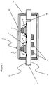
Fig. 2 shows a cross-section of anelectronic module 1 according to some embodiments of the present disclosure. Elements of theelectronic module 1 can be seen in cross-section, and the disclosure inFig. 2 is not meant to be considered in a limiting fashion with regard to positioning and number of theelectronic components 11. Furthermore, theelectronic components 11 are not shown to scale inFig. 2 . - As illustrated in
Fig. 2 , theelectronic module 1 is provided with asubstrate 10 onto which theelectronic components 11 are mounted. The electronic components may comprise capacitors, resistors, amplifiers, digital to analogue converters, semiconductors, ICs, an application-specific integrated circuit (Asic), dies and/or the like. Thesubstrate 10 is not limited in size or shape, and is of course chosen for the particular application required. As can be seen fromFig. 2 , thesubstrate 10 preferably haselectronic components 11 mounted on eachsurface substrate 10. - As shown in
Fig. 2 , certain of theelectronic components 11 are provided withwiring 16 which runs to thesurface substrate 10. Not all of theelectronic components 11 require such wiring, and indeed certainelectronic components 11 may connect to electronic wiring patterns (not shown) on one or other of thesurfaces substrate 10. The nature of connection and patterning of thesubstrate 1 by means of such wiring is not limiting in this case, and any known technology and technique or indeed wiring pattern can be considered. - Whilst in
Fig. 2 thecomponents 11 on thesurface 12 of thesubstrate 10 are provided with thewiring 16 to thesurface 12, this is not intended as a limitation. Indeed, it is a beneficial aspect of the present application that theelectronic components 11 may be positioned on eithersurface substrate 10. As such, in embodiments of the present disclosure, semiconductor ICs, Asics and other dies may like other electronic components be positioned on either thesurface 12 or thesurface 13 of thesubstrate 10. - The nature of the
electronic components 11 is not limiting, and any requiredelectronic components 11 for meeting the desired application of theelectronic module 1 can be included on thesurfaces substrate 10. In particular, theelectronic components 11 may be discrete electronic components, surface mounted components, SMCs, die components, semiconductor ICs and the like. One advantage of the present disclosure is that there is no need to separate out theelectronic components 11 onto one or other of thesurfaces substrate 10, and theelectronic components 11 may be positioned in order to provide the smallest footprint without any interference between one or other of theelectronic components 11. - As shown in
Fig. 2 , theelectronic components 11 may be attached to thesurfaces substrates 10 by means of aglue 14. Theglue 14 is particularly advantageous in theelectronic module 1, as it allows for easy placement of theelectronic components 11. Furthermore, the choice ofglue 14 or epoxy or other adhesive compound, can be chosen for the end environment for theelectronic module 1. Theelectronic module 1 may be designed for/used in a harsh environment, which may be subjected to high temperatures and pressure. The choice ofglue 14 is generally open, however, in some embodiments of the present disclosure, theglue 14 may comprise a glue that has a low or zero solvent content, so that outgassing does not become a problem under high or low pressures and temperatures. Furthermore, theglue 14 will typically have a better temperature response when thesubstrate 10 expands or contracts in different temperature and pressure environments, thus minimizing the drop-off ofelectronic components 11 from the surfaces of thesubstrate 10. - The
substrate 10 in some embodiments of the present disclosure is formed from a ceramic material, wherein the ceramic provides an inert substrate material which is well chosen for the harsh environments in wellbore technologies and applications. In particular, in some embodiments of the present disclosure, thesubstrate 10 may comprise, a high temperature co-fired ceramic (HTCC). As further seen inFig. 2 , connections between theelectronic components 11 on theupper side 12 of thesubstrates 10 to thelower side 13 can be achieved by means offeedthroughs 15. The positioning offeedthroughs 15 is based on the desired structuring and positioning of theelectronic components 11, and in certain circumstances thefeedthroughs 15 will not even be required. - As discussed above, the
electronic components 11 are glued or stuck to thesurfaces substrate 10. In some embodiments of the present disclosure, none of theelectronic components 11 are soldered to thesurfaces substrates 10. Solder is sometimes useful for making electric connections, in other circumstances, however, it is not a particularly temperature stable material. Further, the choice ofglue 14 usually requires that in order to properly cure theglue 14 it is necessary to heat theelectronic module 1 to high temperatures, sometimes higher than the temperatures which theelectronic module 1 will be subject to in use. The solder material can under such circumstances melt or become unstable, thus meaning that if solder is used, it is not possible to fully cure theglue 14 and thecomponents 11 may not be properly attached to thesubstrates 10. - In order to properly protect the
electronic components 11 from the environment in use, a cover surrounding theelectronic components 11 on thesubstrates 10 is provided. The embodiment shown inFig. 2 shows sidewalls 20. Thesidewalls 20 may comprise a metallic ring structure, wherein the metallic ring is positioned generally toward the outer edge of thesubstrate 10. Further, a ceramic ring structure could be used instead of, or in addition to, the metallic ring to form thesidewalls 20. The positioning of thesidewalls 20 is chosen by means of the end use of theelectronic module 1, and may not cover the entire surface of thesubstrate 10. It is advantageous for thesidewalls 20 to be brazed, welded or indeed glued to thesubstrate 10, and in particular to be affixed to thesubstrates 10 prior to attachment of theelectronic components 11. - In order to complete the cover over the
electronic components 11, alid 21 is provided which interacts with thesidewalls 20 in order to provide a hermetic and fluid-tight seal. Thelid 21 may be welded, brazed, sintered, screwed, connected by a glass frit process or even glued to the upper ends of thesidewalls 20, thus leading to the hermetic seal. Additionally, the cavity formed between thesubstrates 10, thesidewalls 20 and thelid 21 can be filled with an inert gas or other material so as to avoid any reaction with theelectronic components 11 when theelectronic module 1 is in position and in use. - An alternative embodiment to using a metal or ceramic ring structure to form the
sidewalls 20 is to use asubstrate 10 that has the sidewalls 20 formed/integrated therein and extending out of the plane of thesubstrate 10 replacing the ring structure. Thesidewalls 20 may comprise a ceramic/metallic material and would perform the same purpose as the structure. Again, thelid 21 would be attached to the top edge of the integrated sidewalls, thus providing for the generation of the cavity. In some embodiments of the present disclosure, thesubstrate 10 is configured such that thesidewalls 20 comprise an H profile to the cross-section of thesubstrate 10. In some embodiments of the present disclosure, thesubstrate 10 and thesidewalls 20 are integrated at manufacture to provide a substrate with an H-shaped profile, i.e., sidewalls projecting out from either surface of the substrate. Theelectronic components 11 can then be mounted within the recesses formed on either side of the central flat interior substrate portion. - The
electronic module 1 shown inFig. 2 can be produced as generally discussed above, and relates to the provision of thesubstrate 10 either as aflat substrate 10, or as the H-profile substrate 10. In embodiments of the present disclosure, theelectronic components 11 are mounted within the central region of thesubstrates 10, and this is either within the preformed sidewalls from the substrate material, or after provision of the metallic ring sidewalls. Theelectronic components 11 are glued into and onto thesubstrate 10 at the desired locations, wherein these locations are determined by means of the eventual requirements from the circuitry, as well as the desire to keep the footprint as small as possible whilst minimising interference between neighbouring components. - After the
electronic components 11 have been positioned onto thesubstrate 10, theglue 14 or epoxy or the like, is appropriately cured at a high temperature. As a result of this curing process at high temperature, solder may not be used in the fixing of theelectronic components 11 to thesubstrates 10. The curedglue 14 or epoxy then has a good bonding strength with thesubstrate 10, however the lack of solder means that no detrimental effects will arise by means of the solder being over heated. In embodiments of the present invention, theelectronic components 11 are either contacted to preformed circuitry on thesubstrate 10, or can be wire bonded to this circuitry as required. In some embodiments, by performing the final steps under an inert atmosphere, it is possible to then apply alid 21 to thesidewalls 20, thus enclosing the circuitry andelectronic components 11 in said inert atmosphere. - The
electronic module 1 as described above, and as constructed by the above method, was tested at a temperature of around 230 degrees centigrade for 1500 hours, and it was found that there were no negative effects to any of theelectronic components 11. Such anelectronic module 1 thus has an expected lifetime of at least 5 years in an environment of 200°C, which is over and above that expected from the prior art double-sided MCMs shown inFig. 1 . Moreover, curing temperatures of over 200, 210, 220, 230, 240 or even 250 degrees centigrade may be used to cure glues attaching theelectronic components 11 to thesubstrate 10. Additionally by hermetically sealing both sides of thesubstrate 10, semiconductor ICs, dies, Asics and/or the like may be disposed on either side of the substrate reducing size of the substrate, allowing the substrate to serve as a shield between the components, allowing gluing of components to both sides of thesubstrate 10 and/or the like. Use of glue for attachment of all electrical components may avoid issues with soldering/forming electrical connections on a ceramic substrate. - Whilst the above has been described in detail, it should not be taken as a limiting combination of features. Indeed, it is to be understood that the above describes a number of features of both the
electronic module 1 and method of making the same, however the skilled would be well aware of the possibility of combining one or other of the aspects into a finalelectronic module 1. Additionally, whilst method steps have been provided, the skilled person would also appreciate that alternatives exist, wherein these alternatives are covered by the claims attached.
Claims (19)
- A packaged electronic module for downhole applications in a borehole, comprising:a substrate comprising a first and a second surface; anda plurality of electronic components, wherein at least one of the plurality of electronic components is located on each of the first and second surfaces, and wherein the plurality of electronic components are attached to the first and second surfaces of the substrate by an adhesive and at least one of the electronic components comprises a multi-chip module and includes one or more of:discrete electronic components;surface mounted components;die components;semiconductor ICs; orsemiconductor chips.
- The packaged electronic module according to claim 1, wherein the adhesive does not comprise solder.
- The packaged electronic module according to any of the preceding claims, wherein the substrate comprises a ceramic material or a high temperature co-fired ceramic.
- The packaged electronic module according to any of the preceding claims, further comprising:metallic or ceramic rings disposed on each of the first and second surfaces, wherein the metallic or ceramic rings extend outward from the first and second surfaces and completely surround the one or more of the electronic components disposed thereon; anda pair of lids, where each of the pair of lids is coupled with a one of the metallic or ceramic rings and configured to cover the one or more electronic components surrounded by the metallic or ceramic rings.
- The packaged electronic module (1) according to claim 4, wherein the metallic rings comprise kovar.
- The packaged electronic module according to claim 4, wherein the each of the pair of lids forms a fluid-tight hermetic seal with the metallic or ceramic rings.
- The packaged electronic module according to any of claims 1 through 3, wherein the substrate comprises sidewalls extending outwards from each of the first and the second surface of the substrate, and wherein the sidewalls on each of the first and the second surfaces are configured to surround the one or more electrical components located thereon.
- The packaged electronic module according to claim 7, further comprising a pair of lids, wherein a first of the pair of lids is coupled with the sidewalls extending from the first surface and is configured to cover the one or more electronic components located on the first surface and a second of the pair of lids is coupled with the sidewalls extending from the second surface and configured to cover the one or more electronic components located on the second surface.
- The packaged electronic module according to claim 8, wherein enclosures formed by the substrate, the sidewalls rings and the pair of lids are filled with an inert gas in order to surround and protect the electronic components therein.
- The packaged electronic module according to any of the preceding claims, wherein the substrate is provided with feed-through channels for electrical connection between the one or more electronic components on the first surface and the one or more electrical components on the second surface.
- The packaged electronic module according to any of the preceding claims, wherein the electronic components are arranged on the first and the second surfaces to prevent interference between said electronic components and/or are arranged on the first and the second surfaces to minimize size of the module.
- The packaged electronic module according to any of the preceding claims, wherein the adhesive comprises a low solvent glue, a solvent free glue and/or a glue that does not produce outgassing during or after curing.
- The packaged electronic module according to any of the preceding claims, wherein the adhesive comprises a glue that does not produce outgassing when cured to a temperature above 200°C, 225°C, 240°C or 250°C.
- The packaged electronic module according to any of the preceding claims, wherein the adhesive comprises a polyimide.
- A method of making an electronic module according to claim 1, the method comprising:providing a substrate; andgluing one or more electrical components to each side of the substrate; andcuring the glue.
- The method according to claim 15, wherein the substrate includes sidewalls on each side of the substrate, and wherein the sidewalls on each side of the substrate extend outwards from the substrate surface and surround a section of the substrate surface forming pockets on each side of the substrate, and wherein the one or more electrical components are glued inside each of the pockets.
- The method according to claim 16, further comprising:attaching lids to the sidewalls on each side of the substrate to cover the one or more electrical components in each of the pockets.
- The method according to 17, further comprising:adding an inert gas inside each of the pockets.
- The method according to claims 15, wherein curing the glue comprises heating the glue to temperatures above 200 °C, 210°C, 220°C, 230 °C, 240°C or 250°C.
Priority Applications (3)
| Application Number | Priority Date | Filing Date | Title |
|---|---|---|---|
| EP16290025.2A EP3203509B1 (en) | 2016-02-04 | 2016-02-04 | Double-sided hermetic multichip module |
| US16/075,359 US11532526B2 (en) | 2016-02-04 | 2017-02-03 | Double-sided hermetic multichip module |
| PCT/US2017/016361 WO2017136632A2 (en) | 2016-02-04 | 2017-02-03 | Double-sided hermetic multichip module |
Applications Claiming Priority (1)
| Application Number | Priority Date | Filing Date | Title |
|---|---|---|---|
| EP16290025.2A EP3203509B1 (en) | 2016-02-04 | 2016-02-04 | Double-sided hermetic multichip module |
Publications (2)
| Publication Number | Publication Date |
|---|---|
| EP3203509A1 true EP3203509A1 (en) | 2017-08-09 |
| EP3203509B1 EP3203509B1 (en) | 2021-01-20 |
Family
ID=55405284
Family Applications (1)
| Application Number | Title | Priority Date | Filing Date |
|---|---|---|---|
| EP16290025.2A Active EP3203509B1 (en) | 2016-02-04 | 2016-02-04 | Double-sided hermetic multichip module |
Country Status (3)
| Country | Link |
|---|---|
| US (1) | US11532526B2 (en) |
| EP (1) | EP3203509B1 (en) |
| WO (1) | WO2017136632A2 (en) |
Cited By (1)
| Publication number | Priority date | Publication date | Assignee | Title |
|---|---|---|---|---|
| GB2565227A (en) * | 2017-07-13 | 2019-02-06 | Dongguan China Advanced Ceramic Tech Co Ltd | Ceramic module for power semiconductor integrated packaging and preparation method thereof |
Families Citing this family (2)
| Publication number | Priority date | Publication date | Assignee | Title |
|---|---|---|---|---|
| JP7406314B2 (en) * | 2019-06-24 | 2023-12-27 | キヤノン株式会社 | electronic modules and equipment |
| CN115394664B (en) * | 2022-08-24 | 2024-03-19 | 广东汇芯半导体有限公司 | A power module manufacturing method and power module including aluminum and ceramic substrates |
Citations (3)
| Publication number | Priority date | Publication date | Assignee | Title |
|---|---|---|---|---|
| US20020050371A1 (en) * | 1993-06-18 | 2002-05-02 | Czjakowski David R. | Radiation shielding of three dimensional multi-chip modules |
| JP2004210805A (en) * | 2002-11-14 | 2004-07-29 | Hitachi Chem Co Ltd | Adhesive film and its use |
| US20130087903A1 (en) * | 2011-10-06 | 2013-04-11 | Schlumberger Technology Corporation | Electronics Packaging For High Temperature Downhole Applications |
Family Cites Families (12)
| Publication number | Priority date | Publication date | Assignee | Title |
|---|---|---|---|---|
| BR0212760A (en) | 2001-09-19 | 2004-12-07 | Aventis Pharma Sa | Chemical compounds |
| WO2005029055A1 (en) | 2003-09-19 | 2005-03-31 | Invitrogen Corporation | Composite compositions for electrophoresis |
| US7363971B2 (en) * | 2003-11-06 | 2008-04-29 | Halliburton Energy Services, Inc. | Method and apparatus for maintaining a multi-chip module at a temperature above downhole temperature |
| US7226985B2 (en) | 2005-07-12 | 2007-06-05 | Eastman Chemical Company | Polyester-polycarbonate compositions |
| US7804172B2 (en) * | 2006-01-10 | 2010-09-28 | Halliburton Energy Services, Inc. | Electrical connections made with dissimilar metals |
| DE102006023680B8 (en) | 2006-04-20 | 2007-09-27 | Nähmaschinenfabrik Emil Stutznäcker GmbH & Co KG | Process for the production of large-area sewing material |
| US7615712B2 (en) * | 2006-10-31 | 2009-11-10 | Smith International, Inc. | Integrated circuit packages including damming and change protection cover for harsh environments |
| JP5367616B2 (en) * | 2009-02-23 | 2013-12-11 | 新光電気工業株式会社 | Wiring board and manufacturing method thereof |
| WO2012135406A2 (en) * | 2011-04-01 | 2012-10-04 | Schlumberger Canada Limited | High density microelectronics packaging |
| US8854178B1 (en) | 2012-06-21 | 2014-10-07 | Disney Enterprises, Inc. | Enabling authentication and/or effectuating events in virtual environments based on shaking patterns and/or environmental information associated with real-world handheld devices |
| JP6301857B2 (en) * | 2015-02-24 | 2018-03-28 | 株式会社東芝 | Semiconductor module |
| JP6613682B2 (en) * | 2015-07-28 | 2019-12-04 | セイコーエプソン株式会社 | Electronic devices, liquid ejection heads. |
-
2016
- 2016-02-04 EP EP16290025.2A patent/EP3203509B1/en active Active
-
2017
- 2017-02-03 US US16/075,359 patent/US11532526B2/en active Active
- 2017-02-03 WO PCT/US2017/016361 patent/WO2017136632A2/en not_active Ceased
Patent Citations (3)
| Publication number | Priority date | Publication date | Assignee | Title |
|---|---|---|---|---|
| US20020050371A1 (en) * | 1993-06-18 | 2002-05-02 | Czjakowski David R. | Radiation shielding of three dimensional multi-chip modules |
| JP2004210805A (en) * | 2002-11-14 | 2004-07-29 | Hitachi Chem Co Ltd | Adhesive film and its use |
| US20130087903A1 (en) * | 2011-10-06 | 2013-04-11 | Schlumberger Technology Corporation | Electronics Packaging For High Temperature Downhole Applications |
Cited By (2)
| Publication number | Priority date | Publication date | Assignee | Title |
|---|---|---|---|---|
| GB2565227A (en) * | 2017-07-13 | 2019-02-06 | Dongguan China Advanced Ceramic Tech Co Ltd | Ceramic module for power semiconductor integrated packaging and preparation method thereof |
| GB2565227B (en) * | 2017-07-13 | 2020-07-15 | Dongguan China Advanced Ceramic Tech Co Ltd | Ceramic module for power semiconductor integrated packaging and preparation method thereof |
Also Published As
| Publication number | Publication date |
|---|---|
| WO2017136632A2 (en) | 2017-08-10 |
| US20190348334A1 (en) | 2019-11-14 |
| US11532526B2 (en) | 2022-12-20 |
| WO2017136632A3 (en) | 2018-07-26 |
| EP3203509B1 (en) | 2021-01-20 |
Similar Documents
| Publication | Publication Date | Title |
|---|---|---|
| EP0421005B1 (en) | Process of assembling an electronic package | |
| US5939772A (en) | Shielded package for magnetic devices | |
| US8853839B2 (en) | Air-release features in cavity packages | |
| US11699670B2 (en) | High-frequency module | |
| US20200381336A1 (en) | High-frequency module | |
| CA2453003A1 (en) | Use of diverse materials in air-cavity packaging of electronic devices | |
| US20180352666A1 (en) | Electronic Module and Method for Producing an Electronic Module having a Fluid-Tight Housing | |
| JPH06275773A (en) | Surface mount-able integrated package having integrated battery mount | |
| US11532526B2 (en) | Double-sided hermetic multichip module | |
| US8258013B1 (en) | Integrated circuit assembly having vented heat-spreader | |
| CN106373947A (en) | Robust high performance semiconductor package | |
| WO2022042309A1 (en) | Package housing, waterproof air pressure sensor, and electronic device | |
| CN106068682B (en) | Electronic control module and its manufacturing method | |
| CN209128031U (en) | Microelectronic device | |
| CN108074875A (en) | Semiconductor device package and method of manufacturing the same | |
| JP6991253B2 (en) | Electronic device package and its manufacturing method | |
| US6229088B1 (en) | Low profile electronic enclosure | |
| US7524704B2 (en) | Method for encapsulating a component, especially an electric or electronic component, by means of an improved solder seam | |
| JP2010183349A (en) | Crystal oscillator for surface mount | |
| US10485107B2 (en) | Downhole equipment using flexible circuits | |
| EP4080551B1 (en) | Semiconductor power module and method for manufacturing a semiconductor power module and semiconductor power device | |
| JP2010093206A (en) | High-frequency circuit package | |
| US20050178820A1 (en) | Microsystem enclosure and method of hermetic sealing | |
| CN116134604A (en) | Substrate including lid structure, package substrate including substrate, and semiconductor device | |
| JP2005072421A (en) | Electronic component storage package and electronic device |
Legal Events
| Date | Code | Title | Description |
|---|---|---|---|
| PUAI | Public reference made under article 153(3) epc to a published international application that has entered the european phase |
Free format text: ORIGINAL CODE: 0009012 |
|
| STAA | Information on the status of an ep patent application or granted ep patent |
Free format text: STATUS: THE APPLICATION HAS BEEN PUBLISHED |
|
| AK | Designated contracting states |
Kind code of ref document: A1 Designated state(s): AL AT BE BG CH CY CZ DE DK EE ES FI FR GB GR HR HU IE IS IT LI LT LU LV MC MK MT NL NO PL PT RO RS SE SI SK SM TR |
|
| AX | Request for extension of the european patent |
Extension state: BA ME |
|
| STAA | Information on the status of an ep patent application or granted ep patent |
Free format text: STATUS: REQUEST FOR EXAMINATION WAS MADE |
|
| 17P | Request for examination filed |
Effective date: 20180529 |
|
| RBV | Designated contracting states (corrected) |
Designated state(s): AL AT BE BG CH CY CZ DE DK EE ES FI FR GB GR HR HU IE IS IT LI LT LU LV MC MK MT NL NO PL PT RO RS SE SI SK SM TR |
|
| STAA | Information on the status of an ep patent application or granted ep patent |
Free format text: STATUS: EXAMINATION IS IN PROGRESS |
|
| 17Q | First examination report despatched |
Effective date: 20190410 |
|
| GRAP | Despatch of communication of intention to grant a patent |
Free format text: ORIGINAL CODE: EPIDOSNIGR1 |
|
| STAA | Information on the status of an ep patent application or granted ep patent |
Free format text: STATUS: GRANT OF PATENT IS INTENDED |
|
| INTG | Intention to grant announced |
Effective date: 20200810 |
|
| GRAS | Grant fee paid |
Free format text: ORIGINAL CODE: EPIDOSNIGR3 |
|
| GRAA | (expected) grant |
Free format text: ORIGINAL CODE: 0009210 |
|
| STAA | Information on the status of an ep patent application or granted ep patent |
Free format text: STATUS: THE PATENT HAS BEEN GRANTED |
|
| AK | Designated contracting states |
Kind code of ref document: B1 Designated state(s): AL AT BE BG CH CY CZ DE DK EE ES FI FR GB GR HR HU IE IS IT LI LT LU LV MC MK MT NL NO PL PT RO RS SE SI SK SM TR |
|
| REG | Reference to a national code |
Ref country code: GB Ref legal event code: FG4D |
|
| REG | Reference to a national code |
Ref country code: CH Ref legal event code: EP |
|
| REG | Reference to a national code |
Ref country code: DE Ref legal event code: R096 Ref document number: 602016051638 Country of ref document: DE |
|
| REG | Reference to a national code |
Ref country code: AT Ref legal event code: REF Ref document number: 1357114 Country of ref document: AT Kind code of ref document: T Effective date: 20210215 |
|
| REG | Reference to a national code |
Ref country code: IE Ref legal event code: FG4D |
|
| REG | Reference to a national code |
Ref country code: NL Ref legal event code: MP Effective date: 20210120 |
|
| REG | Reference to a national code |
Ref country code: NO Ref legal event code: T2 Effective date: 20210120 |
|
| REG | Reference to a national code |
Ref country code: LT Ref legal event code: MG9D |
|
| REG | Reference to a national code |
Ref country code: AT Ref legal event code: MK05 Ref document number: 1357114 Country of ref document: AT Kind code of ref document: T Effective date: 20210120 |
|
| PG25 | Lapsed in a contracting state [announced via postgrant information from national office to epo] |
Ref country code: PT Free format text: LAPSE BECAUSE OF FAILURE TO SUBMIT A TRANSLATION OF THE DESCRIPTION OR TO PAY THE FEE WITHIN THE PRESCRIBED TIME-LIMIT Effective date: 20210520 Ref country code: HR Free format text: LAPSE BECAUSE OF FAILURE TO SUBMIT A TRANSLATION OF THE DESCRIPTION OR TO PAY THE FEE WITHIN THE PRESCRIBED TIME-LIMIT Effective date: 20210120 Ref country code: FI Free format text: LAPSE BECAUSE OF FAILURE TO SUBMIT A TRANSLATION OF THE DESCRIPTION OR TO PAY THE FEE WITHIN THE PRESCRIBED TIME-LIMIT Effective date: 20210120 Ref country code: GR Free format text: LAPSE BECAUSE OF FAILURE TO SUBMIT A TRANSLATION OF THE DESCRIPTION OR TO PAY THE FEE WITHIN THE PRESCRIBED TIME-LIMIT Effective date: 20210421 Ref country code: BG Free format text: LAPSE BECAUSE OF FAILURE TO SUBMIT A TRANSLATION OF THE DESCRIPTION OR TO PAY THE FEE WITHIN THE PRESCRIBED TIME-LIMIT Effective date: 20210420 Ref country code: LT Free format text: LAPSE BECAUSE OF FAILURE TO SUBMIT A TRANSLATION OF THE DESCRIPTION OR TO PAY THE FEE WITHIN THE PRESCRIBED TIME-LIMIT Effective date: 20210120 |
|
| PG25 | Lapsed in a contracting state [announced via postgrant information from national office to epo] |
Ref country code: SE Free format text: LAPSE BECAUSE OF FAILURE TO SUBMIT A TRANSLATION OF THE DESCRIPTION OR TO PAY THE FEE WITHIN THE PRESCRIBED TIME-LIMIT Effective date: 20210120 Ref country code: AT Free format text: LAPSE BECAUSE OF FAILURE TO SUBMIT A TRANSLATION OF THE DESCRIPTION OR TO PAY THE FEE WITHIN THE PRESCRIBED TIME-LIMIT Effective date: 20210120 Ref country code: PL Free format text: LAPSE BECAUSE OF FAILURE TO SUBMIT A TRANSLATION OF THE DESCRIPTION OR TO PAY THE FEE WITHIN THE PRESCRIBED TIME-LIMIT Effective date: 20210120 Ref country code: RS Free format text: LAPSE BECAUSE OF FAILURE TO SUBMIT A TRANSLATION OF THE DESCRIPTION OR TO PAY THE FEE WITHIN THE PRESCRIBED TIME-LIMIT Effective date: 20210120 Ref country code: LV Free format text: LAPSE BECAUSE OF FAILURE TO SUBMIT A TRANSLATION OF THE DESCRIPTION OR TO PAY THE FEE WITHIN THE PRESCRIBED TIME-LIMIT Effective date: 20210120 |
|
| PG25 | Lapsed in a contracting state [announced via postgrant information from national office to epo] |
Ref country code: IS Free format text: LAPSE BECAUSE OF FAILURE TO SUBMIT A TRANSLATION OF THE DESCRIPTION OR TO PAY THE FEE WITHIN THE PRESCRIBED TIME-LIMIT Effective date: 20210520 |
|
| REG | Reference to a national code |
Ref country code: DE Ref legal event code: R097 Ref document number: 602016051638 Country of ref document: DE |
|
| REG | Reference to a national code |
Ref country code: BE Ref legal event code: MM Effective date: 20210228 |
|
| PG25 | Lapsed in a contracting state [announced via postgrant information from national office to epo] |
Ref country code: LU Free format text: LAPSE BECAUSE OF NON-PAYMENT OF DUE FEES Effective date: 20210204 Ref country code: LI Free format text: LAPSE BECAUSE OF NON-PAYMENT OF DUE FEES Effective date: 20210228 Ref country code: MC Free format text: LAPSE BECAUSE OF FAILURE TO SUBMIT A TRANSLATION OF THE DESCRIPTION OR TO PAY THE FEE WITHIN THE PRESCRIBED TIME-LIMIT Effective date: 20210120 Ref country code: CZ Free format text: LAPSE BECAUSE OF FAILURE TO SUBMIT A TRANSLATION OF THE DESCRIPTION OR TO PAY THE FEE WITHIN THE PRESCRIBED TIME-LIMIT Effective date: 20210120 Ref country code: EE Free format text: LAPSE BECAUSE OF FAILURE TO SUBMIT A TRANSLATION OF THE DESCRIPTION OR TO PAY THE FEE WITHIN THE PRESCRIBED TIME-LIMIT Effective date: 20210120 Ref country code: CH Free format text: LAPSE BECAUSE OF NON-PAYMENT OF DUE FEES Effective date: 20210228 Ref country code: SM Free format text: LAPSE BECAUSE OF FAILURE TO SUBMIT A TRANSLATION OF THE DESCRIPTION OR TO PAY THE FEE WITHIN THE PRESCRIBED TIME-LIMIT Effective date: 20210120 |
|
| PLBE | No opposition filed within time limit |
Free format text: ORIGINAL CODE: 0009261 |
|
| STAA | Information on the status of an ep patent application or granted ep patent |
Free format text: STATUS: NO OPPOSITION FILED WITHIN TIME LIMIT |
|
| PG25 | Lapsed in a contracting state [announced via postgrant information from national office to epo] |
Ref country code: SK Free format text: LAPSE BECAUSE OF FAILURE TO SUBMIT A TRANSLATION OF THE DESCRIPTION OR TO PAY THE FEE WITHIN THE PRESCRIBED TIME-LIMIT Effective date: 20210120 Ref country code: RO Free format text: LAPSE BECAUSE OF FAILURE TO SUBMIT A TRANSLATION OF THE DESCRIPTION OR TO PAY THE FEE WITHIN THE PRESCRIBED TIME-LIMIT Effective date: 20210120 Ref country code: DK Free format text: LAPSE BECAUSE OF FAILURE TO SUBMIT A TRANSLATION OF THE DESCRIPTION OR TO PAY THE FEE WITHIN THE PRESCRIBED TIME-LIMIT Effective date: 20210120 |
|
| 26N | No opposition filed |
Effective date: 20211021 |
|
| PG25 | Lapsed in a contracting state [announced via postgrant information from national office to epo] |
Ref country code: AL Free format text: LAPSE BECAUSE OF FAILURE TO SUBMIT A TRANSLATION OF THE DESCRIPTION OR TO PAY THE FEE WITHIN THE PRESCRIBED TIME-LIMIT Effective date: 20210120 Ref country code: ES Free format text: LAPSE BECAUSE OF FAILURE TO SUBMIT A TRANSLATION OF THE DESCRIPTION OR TO PAY THE FEE WITHIN THE PRESCRIBED TIME-LIMIT Effective date: 20210120 Ref country code: FR Free format text: LAPSE BECAUSE OF NON-PAYMENT OF DUE FEES Effective date: 20210320 Ref country code: IE Free format text: LAPSE BECAUSE OF NON-PAYMENT OF DUE FEES Effective date: 20210204 |
|
| PG25 | Lapsed in a contracting state [announced via postgrant information from national office to epo] |
Ref country code: SI Free format text: LAPSE BECAUSE OF FAILURE TO SUBMIT A TRANSLATION OF THE DESCRIPTION OR TO PAY THE FEE WITHIN THE PRESCRIBED TIME-LIMIT Effective date: 20210120 |
|
| PG25 | Lapsed in a contracting state [announced via postgrant information from national office to epo] |
Ref country code: IT Free format text: LAPSE BECAUSE OF FAILURE TO SUBMIT A TRANSLATION OF THE DESCRIPTION OR TO PAY THE FEE WITHIN THE PRESCRIBED TIME-LIMIT Effective date: 20210120 |
|
| PG25 | Lapsed in a contracting state [announced via postgrant information from national office to epo] |
Ref country code: IS Free format text: LAPSE BECAUSE OF FAILURE TO SUBMIT A TRANSLATION OF THE DESCRIPTION OR TO PAY THE FEE WITHIN THE PRESCRIBED TIME-LIMIT Effective date: 20210520 |
|
| PG25 | Lapsed in a contracting state [announced via postgrant information from national office to epo] |
Ref country code: BE Free format text: LAPSE BECAUSE OF NON-PAYMENT OF DUE FEES Effective date: 20210228 |
|
| PG25 | Lapsed in a contracting state [announced via postgrant information from national office to epo] |
Ref country code: HU Free format text: LAPSE BECAUSE OF FAILURE TO SUBMIT A TRANSLATION OF THE DESCRIPTION OR TO PAY THE FEE WITHIN THE PRESCRIBED TIME-LIMIT; INVALID AB INITIO Effective date: 20160204 |
|
| PG25 | Lapsed in a contracting state [announced via postgrant information from national office to epo] |
Ref country code: NL Free format text: LAPSE BECAUSE OF NON-PAYMENT OF DUE FEES Effective date: 20210120 Ref country code: CY Free format text: LAPSE BECAUSE OF FAILURE TO SUBMIT A TRANSLATION OF THE DESCRIPTION OR TO PAY THE FEE WITHIN THE PRESCRIBED TIME-LIMIT Effective date: 20210120 |
|
| P01 | Opt-out of the competence of the unified patent court (upc) registered |
Effective date: 20231208 |
|
| PG25 | Lapsed in a contracting state [announced via postgrant information from national office to epo] |
Ref country code: MK Free format text: LAPSE BECAUSE OF FAILURE TO SUBMIT A TRANSLATION OF THE DESCRIPTION OR TO PAY THE FEE WITHIN THE PRESCRIBED TIME-LIMIT Effective date: 20210120 |
|
| PG25 | Lapsed in a contracting state [announced via postgrant information from national office to epo] |
Ref country code: TR Free format text: LAPSE BECAUSE OF FAILURE TO SUBMIT A TRANSLATION OF THE DESCRIPTION OR TO PAY THE FEE WITHIN THE PRESCRIBED TIME-LIMIT Effective date: 20210120 |
|
| PG25 | Lapsed in a contracting state [announced via postgrant information from national office to epo] |
Ref country code: MT Free format text: LAPSE BECAUSE OF FAILURE TO SUBMIT A TRANSLATION OF THE DESCRIPTION OR TO PAY THE FEE WITHIN THE PRESCRIBED TIME-LIMIT Effective date: 20210120 |
|
| PGFP | Annual fee paid to national office [announced via postgrant information from national office to epo] |
Ref country code: DE Payment date: 20241210 Year of fee payment: 10 |
|
| REG | Reference to a national code |
Ref country code: DE Ref legal event code: R079 Ref document number: 602016051638 Country of ref document: DE Free format text: PREVIOUS MAIN CLASS: H01L0023055000 Ipc: H10W0076153000 |
|
| PGFP | Annual fee paid to national office [announced via postgrant information from national office to epo] |
Ref country code: GB Payment date: 20260223 Year of fee payment: 11 |
|
| PGFP | Annual fee paid to national office [announced via postgrant information from national office to epo] |
Ref country code: NO Payment date: 20260218 Year of fee payment: 11 |