EP3203322A1 - Mark structure and fabrication method thereof - Google Patents
Mark structure and fabrication method thereof Download PDFInfo
- Publication number
- EP3203322A1 EP3203322A1 EP17152668.4A EP17152668A EP3203322A1 EP 3203322 A1 EP3203322 A1 EP 3203322A1 EP 17152668 A EP17152668 A EP 17152668A EP 3203322 A1 EP3203322 A1 EP 3203322A1
- Authority
- EP
- European Patent Office
- Prior art keywords
- mark
- layer
- opening
- dielectric layer
- region
- Prior art date
- Legal status (The legal status is an assumption and is not a legal conclusion. Google has not performed a legal analysis and makes no representation as to the accuracy of the status listed.)
- Granted
Links
Images




Classifications
-
- G—PHYSICS
- G03—PHOTOGRAPHY; CINEMATOGRAPHY; ANALOGOUS TECHNIQUES USING WAVES OTHER THAN OPTICAL WAVES; ELECTROGRAPHY; HOLOGRAPHY
- G03F—PHOTOMECHANICAL PRODUCTION OF TEXTURED OR PATTERNED SURFACES, e.g. FOR PRINTING, FOR PROCESSING OF SEMICONDUCTOR DEVICES; MATERIALS THEREFOR; ORIGINALS THEREFOR; APPARATUS SPECIALLY ADAPTED THEREFOR
- G03F7/00—Photomechanical, e.g. photolithographic, production of textured or patterned surfaces, e.g. printing surfaces; Materials therefor, e.g. comprising photoresists; Apparatus specially adapted therefor
- G03F7/70—Microphotolithographic exposure; Apparatus therefor
- G03F7/70483—Information management; Active and passive control; Testing; Wafer monitoring, e.g. pattern monitoring
- G03F7/70605—Workpiece metrology
- G03F7/70616—Monitoring the printed patterns
- G03F7/70633—Overlay, i.e. relative alignment between patterns printed by separate exposures in different layers, or in the same layer in multiple exposures or stitching
-
- G—PHYSICS
- G03—PHOTOGRAPHY; CINEMATOGRAPHY; ANALOGOUS TECHNIQUES USING WAVES OTHER THAN OPTICAL WAVES; ELECTROGRAPHY; HOLOGRAPHY
- G03F—PHOTOMECHANICAL PRODUCTION OF TEXTURED OR PATTERNED SURFACES, e.g. FOR PRINTING, FOR PROCESSING OF SEMICONDUCTOR DEVICES; MATERIALS THEREFOR; ORIGINALS THEREFOR; APPARATUS SPECIALLY ADAPTED THEREFOR
- G03F7/00—Photomechanical, e.g. photolithographic, production of textured or patterned surfaces, e.g. printing surfaces; Materials therefor, e.g. comprising photoresists; Apparatus specially adapted therefor
- G03F7/70—Microphotolithographic exposure; Apparatus therefor
- G03F7/70483—Information management; Active and passive control; Testing; Wafer monitoring, e.g. pattern monitoring
- G03F7/70605—Workpiece metrology
- G03F7/70681—Metrology strategies
- G03F7/70683—Mark designs
-
- G—PHYSICS
- G03—PHOTOGRAPHY; CINEMATOGRAPHY; ANALOGOUS TECHNIQUES USING WAVES OTHER THAN OPTICAL WAVES; ELECTROGRAPHY; HOLOGRAPHY
- G03F—PHOTOMECHANICAL PRODUCTION OF TEXTURED OR PATTERNED SURFACES, e.g. FOR PRINTING, FOR PROCESSING OF SEMICONDUCTOR DEVICES; MATERIALS THEREFOR; ORIGINALS THEREFOR; APPARATUS SPECIALLY ADAPTED THEREFOR
- G03F9/00—Registration or positioning of originals, masks, frames, photographic sheets or textured or patterned surfaces, e.g. automatically
- G03F9/70—Registration or positioning of originals, masks, frames, photographic sheets or textured or patterned surfaces, e.g. automatically for microlithography
- G03F9/7073—Alignment marks and their environment
- G03F9/708—Mark formation
-
- G—PHYSICS
- G03—PHOTOGRAPHY; CINEMATOGRAPHY; ANALOGOUS TECHNIQUES USING WAVES OTHER THAN OPTICAL WAVES; ELECTROGRAPHY; HOLOGRAPHY
- G03F—PHOTOMECHANICAL PRODUCTION OF TEXTURED OR PATTERNED SURFACES, e.g. FOR PRINTING, FOR PROCESSING OF SEMICONDUCTOR DEVICES; MATERIALS THEREFOR; ORIGINALS THEREFOR; APPARATUS SPECIALLY ADAPTED THEREFOR
- G03F9/00—Registration or positioning of originals, masks, frames, photographic sheets or textured or patterned surfaces, e.g. automatically
- G03F9/70—Registration or positioning of originals, masks, frames, photographic sheets or textured or patterned surfaces, e.g. automatically for microlithography
- G03F9/7088—Alignment mark detection, e.g. TTR, TTL, off-axis detection, array detector, video detection
-
- H—ELECTRICITY
- H10—SEMICONDUCTOR DEVICES; ELECTRIC SOLID-STATE DEVICES NOT OTHERWISE PROVIDED FOR
- H10P—GENERIC PROCESSES OR APPARATUS FOR THE MANUFACTURE OR TREATMENT OF DEVICES COVERED BY CLASS H10
- H10P50/00—Etching of wafers, substrates or parts of devices
- H10P50/20—Dry etching; Plasma etching; Reactive-ion etching
- H10P50/28—Dry etching; Plasma etching; Reactive-ion etching of insulating materials
- H10P50/282—Dry etching; Plasma etching; Reactive-ion etching of insulating materials of inorganic materials
- H10P50/283—Dry etching; Plasma etching; Reactive-ion etching of insulating materials of inorganic materials by chemical means
-
- H—ELECTRICITY
- H10—SEMICONDUCTOR DEVICES; ELECTRIC SOLID-STATE DEVICES NOT OTHERWISE PROVIDED FOR
- H10P—GENERIC PROCESSES OR APPARATUS FOR THE MANUFACTURE OR TREATMENT OF DEVICES COVERED BY CLASS H10
- H10P50/00—Etching of wafers, substrates or parts of devices
- H10P50/73—Etching of wafers, substrates or parts of devices using masks for insulating materials
-
- H—ELECTRICITY
- H10—SEMICONDUCTOR DEVICES; ELECTRIC SOLID-STATE DEVICES NOT OTHERWISE PROVIDED FOR
- H10W—GENERIC PACKAGES, INTERCONNECTIONS, CONNECTORS OR OTHER CONSTRUCTIONAL DETAILS OF DEVICES COVERED BY CLASS H10
- H10W20/00—Interconnections in chips, wafers or substrates
- H10W20/01—Manufacture or treatment
- H10W20/031—Manufacture or treatment of conductive parts of the interconnections
- H10W20/056—Manufacture or treatment of conductive parts of the interconnections by filling conductive material into holes, grooves or trenches
-
- H—ELECTRICITY
- H10—SEMICONDUCTOR DEVICES; ELECTRIC SOLID-STATE DEVICES NOT OTHERWISE PROVIDED FOR
- H10W—GENERIC PACKAGES, INTERCONNECTIONS, CONNECTORS OR OTHER CONSTRUCTIONAL DETAILS OF DEVICES COVERED BY CLASS H10
- H10W20/00—Interconnections in chips, wafers or substrates
- H10W20/01—Manufacture or treatment
- H10W20/071—Manufacture or treatment of dielectric parts thereof
- H10W20/081—Manufacture or treatment of dielectric parts thereof by forming openings in the dielectric parts
-
- H—ELECTRICITY
- H10—SEMICONDUCTOR DEVICES; ELECTRIC SOLID-STATE DEVICES NOT OTHERWISE PROVIDED FOR
- H10W—GENERIC PACKAGES, INTERCONNECTIONS, CONNECTORS OR OTHER CONSTRUCTIONAL DETAILS OF DEVICES COVERED BY CLASS H10
- H10W20/00—Interconnections in chips, wafers or substrates
- H10W20/40—Interconnections external to wafers or substrates, e.g. back-end-of-line [BEOL] metallisations or vias connecting to gate electrodes
- H10W20/41—Interconnections external to wafers or substrates, e.g. back-end-of-line [BEOL] metallisations or vias connecting to gate electrodes characterised by their conductive parts
- H10W20/43—Layouts of interconnections
-
- H—ELECTRICITY
- H10—SEMICONDUCTOR DEVICES; ELECTRIC SOLID-STATE DEVICES NOT OTHERWISE PROVIDED FOR
- H10W—GENERIC PACKAGES, INTERCONNECTIONS, CONNECTORS OR OTHER CONSTRUCTIONAL DETAILS OF DEVICES COVERED BY CLASS H10
- H10W46/00—Marks applied to devices, e.g. for alignment or identification
-
- H—ELECTRICITY
- H10—SEMICONDUCTOR DEVICES; ELECTRIC SOLID-STATE DEVICES NOT OTHERWISE PROVIDED FOR
- H10W—GENERIC PACKAGES, INTERCONNECTIONS, CONNECTORS OR OTHER CONSTRUCTIONAL DETAILS OF DEVICES COVERED BY CLASS H10
- H10W46/00—Marks applied to devices, e.g. for alignment or identification
- H10W46/301—Marks applied to devices, e.g. for alignment or identification for alignment
-
- H—ELECTRICITY
- H10—SEMICONDUCTOR DEVICES; ELECTRIC SOLID-STATE DEVICES NOT OTHERWISE PROVIDED FOR
- H10W—GENERIC PACKAGES, INTERCONNECTIONS, CONNECTORS OR OTHER CONSTRUCTIONAL DETAILS OF DEVICES COVERED BY CLASS H10
- H10W46/00—Marks applied to devices, e.g. for alignment or identification
- H10W46/501—Marks applied to devices, e.g. for alignment or identification for use before dicing
- H10W46/503—Located in scribe lines
Definitions
- the present invention generally relates to the field of semiconductor manufacturing technology and, more particularly, relates to mark structures and fabrication processes thereof.
- a layout design of the wafer is necessary to divide the wafer into a plurality of dies and a plurality of scribe lanes among adjacent dies.
- the dies are used to subsequently form the semiconductor devices; and the scribe lanes are used as cutting lines when the dies are packaged after forming the semiconductor devices.
- Dividing the surface of the wafer into the dies and scribe lanes is often achieved by transferring patterns on a mask of a photolithography process to the surface of the wafer.
- the process for dividing the surface of the wafer into the dies and the scribe lanes includes forming a photoresist layer on the surface of the wafer by a spin-coating process; installing the wafer having the photoresist layer into an exposure apparatus after baking the photoresist layer; exposing the baked photoresist to transfer the patterns on the mask to the photoresist layer by an exposure process; post-baking the exposed photoresist layer; and developing the post-baked photoresist layer to form the patterns in the photoresist layer.
- the required patterns of the photolithography process such as alignment marks and overlay marks, etc.
- the photoresist often has offset, rotation, shrinking and extending, and/or orthogonal change, etc., during the overlay exposure process because of the overlay precision, wafer shift and focusing precision, etc.
- an overlay measuring mark is required for measuring the exposure error between different dies formed in a same photoresist layer, and/or the exposure error between the dies at a same position of different photoresist layers. By doing so, the overlay precision of the wafer is obtained.
- the disclosed device structures and methods are directed to solve one or more problems set forth above and other problems in the art.
- a first aspect of the present invention provides a method for fabricating a mark structure.
- the method includes: providing a substrate having a device region and a mark region including a first mark region and a second mark region surrounded by the first mark region; sequentially forming a device layer, a dielectric layer and a mask layer over a surface of the substrate; forming a first opening in the dielectric layer in the device region, a first mark in the dielectric layer in the first mark region, and a mark opening in the dielectric layer in the second mark region, a bottom of the first opening, a bottom of the first mark and a bottom of the mark opening being lower than a surface of the dielectric layer and higher than a surface of the device layer; forming a second opening exposing the device layer in the dielectric layer on the bottom of the first opening and a second mark in the dielectric layer on the bottom of the mark opening; and forming a conductive structure in the first opening and the second opening.
- the first mark includes a plurality of first mark trenches.
- forming the first mark, the first opening, and the first mark opening comprises: forming a first pattern layer exposing portions of a surface of the mask layer corresponding to the first mark trenches, the first opening, and the mark opening on the surface of the mask layer; etching the mask layer and portions of the dielectric layer by a first etching process using the first pattern layer as an etching mask; and removing the first pattern layer.
- the first mark includes a plurality of first mark protruding parts.
- forming the first mark, the first opening, and the first mark opening comprises: forming a first pattern layer exposing an entire portion of a surface of the mask layer in the second mark region and portions of the surface of the mask layer in the device region and the first mark region, and covering a portion of the surface of the mask layer corresponding to the first mark protruding parts on the surface of the mask layer; etching the mask layer and portions of the dielectric layer by a first etching process using the first pattern layer as an etching mask; and removing the first pattern layer.
- the second mark preferably includes a plurality of second mark trenches.
- Forming the second mark and the second opening may further comprise: forming a second pattern layer exposing portions of a surface of the dielectric layer corresponding to the second mark trenches and the second opening on the mask layer; etching the dielectric layer by a second etching process using the second pattern layer as an etching mask; and removing the second pattern layer; wherein preferably: an etching rate of the first etching process to the mask layer is greater than an etching rate of the second etching process to the mask layer.
- a second aspect of the present invention provides a mark structure.
- the mask structure includes a substrate having a device region and a mark region including a first mark region and a second mark region surrounded by the first mark region; a device layer formed on a surface of the substrate; a dielectric layer formed on a surface of the device layer; a plurality of first marks formed in the dielectric layer in the first mark region; a plurality of second marks formed in the dielectric layer in the second mark region; and a conductive structure electrically connected with the device layer formed in in the dielectric layer in the device region.
- the conductive structure further comprises: a mask layer on a surface of the dielectric layer; a first opening in the dielectric layer in the device region, the plurality of the first marks in the dielectric layer in the first mark region, and a mark opening in dielectric layer in the second mark region, a bottom of the first opening, a bottom of the first marks and a bottom of the mark opening being lower than the surface of the dielectric layer, and higher than a surface of the device layer; a second opening exposing the device layer in the dielectric layer on the bottom of the first opening and the plurality of second marks in the dielectric layer on the bottom of the mark opening; and a conductive material in the first opening and the second opening.
- the plurality of first marks are uniformly distributed around the second mark region.
- a number of the plurality of first marks is four; a top of each first mark is stripe-shaped; and the four first marks are distributed as a quadrangle around the second mark region.
- a number of the plurality of second marks is four; a top of each second mark is stripe-shaped; and the four second marks are distributed as or form a quadrangle around a center of the second mark region.
- the dielectric layer comprises: a barrier layer formed on the surface of the device layer; a first dielectric layer formed on a surface of the barrier layer; and a second dielectric layer formed on a surface of the first dielectric layer.
- the barrier layer may be made of an N-containing material.
- the first dielectric layer may be made of a ultra-low-K dielectric material.
- the second dielectric layer may be made of tetraethyl orthosilicate.
- the first marks may be first mark protruding parts or, alternatively, the first marks may be first mark trenches.
- the second marks are second mark trenches.
- the mark opening covers the entire second mark region; and side surfaces of the mark opening are side surfaces of the first marks.
- a mark structure according to the second aspect of the present invention is obtainable by a method of the first aspect of the present invention.
- Figures 1-4 illustrate structures corresponding to certain stages of an existing fabrication process of an overlay mark structure.
- the fabrication process includes providing a substrate 100.
- the substrate 100 includes a mark region 110 and a device region 120.
- a device layer 101 is formed on the surface of the substrate 100 in the device region 120; and a dielectric layer 102 is formed on the surface of the device layer 101 and the surface of the substrate 100.
- a mask layer 103 is formed on the surface of the dielectric layer 102.
- a first opening 121 is formed in the device region 120 and a plurality of first mark trenches 111 are formed in the mark region 110 by etching the mask layer 103 and the dielectric layer 102.
- the number of the first mark trenches 111 is four; and the four first mark trenches 111 form a quadrangle.
- Figure 4 is a top view of the structure illustrated in Figure 3 ).
- a plurality of the second mark trenches 112 are formed in the region enclosed by the plurality of first mark trenches 111; and a second opening 122 is formed on the bottom of the first opening 121.
- the second opening 122 exposes the device layer 101.
- the plurality of second mark trenches 122 and the second opening 122 are formed by etching the mask layer 103 in the mark region 110 and the bottom of the first opening 121 using a second etching process.
- the first mark trenches 111 and the second mark trenches 112 form an overlay mark structure.
- the first mark trenches 111 are used to define the position of the first opening 121; and the second mark trenches 112 are used to define the positon of the second opening 122.
- the offset between the first opening 121 and the second opening 122 is obtained.
- the fabrication process can be improved according to the obtained offset.
- the first opening 121 and the second opening 122 are used to form a conductive structure used to electrically connect with the conductive layer 101; and the process for forming the conductive structure is applicable to form structures with a relatively small feature size. Because the second opening 122 needs to expose the surface of the device layer 101 to achieve an electrical connection between the conductive structure and the device layer 101, the first opening 101 needs to be aligned with the device layer 101; and the second opening 122 also needs to be aligned with the conductive layer 101.
- the position of the second opening 122 needs to be determined by the first opening 121.
- the second opening 122 would have a larger offset relative to the device layer 101 if the second opening 122 has an offset relative to the first opening 121.
- Such a larger offset easily causes the bottom of the second opening 122 not to be able to precisely expose the device layer 101.
- it is not allowable to have gradual offsets among the device layer 101, the second opening 122 and the first opening 121 along one direction.
- the fabrication process needs to be adjusted according to the overlay precision. Specifically, the fabrication process is improved by accurately measuring the offset of the relative position between the first opening 121 and the second opening 122; and by learning the offset situation of the relative position between the first opening 121 and the second opening 122. Thus, the detection of the overlay precision between the first opening 121 and the second opening 122 has higher requirements.
- the first etching process is used to etch the mask layer 103 and a portion of the dielectric layer 102 to form the first opening 121.
- the first etching process has a relatively large etching rate to both the mask layer 103 and the dielectric layer 102.
- the depth of the first mark trenches 111 is relatively large; and the bottom of the first mark trenches 111 is lower than the surface of the dielectric layer 102.
- the second etching process is used to etch the dielectric layer 102 on the bottom of the first opening 121, the second etching process has a larger etching rate to the dielectric layer 102 than to the mask layer 103.
- Such an etching rate difference causes the depth of the second mark trenches 112 formed on the mark region 110 is relatively small; or even is unable to penetrate through mask layer 103 to expose the dielectric layer 102.
- the patterns of the second mark trenches 112 are blurry.
- the second mark trenches 112 are completely removed; and the overlay precision between the first mark trenches 111 and the second mark trenches 112 may not be measured.
- the fabrication process of the devices is affected.
- Figure 15 illustrates an exemplary fabrication process of a mark structure consistent with the disclosed embodiments; and Figures 5-9 illustrate structures corresponding to certain stages of the exemplary fabrication process.
- FIG. 15 As shown in Figure 15 , at the beginning of the fabrication process, a substrate with certain structures is provided (S101). Figure 5 illustrates a corresponding structure.
- the substrate 200 may include a mark region (not labeled) and a device region 240.
- the mark region may include a first mark region 250 and a second mark region 260.
- the first mark region 250 may surround the second mark region 260.
- a device layer 210 may be formed on the surface of the substrate 200.
- a dielectric layer 220 may be formed on the surface of the device layer 210.
- a mask layer 230 may be formed on the surface of the dielectric layer 220.
- the device layer 210 may have a conductive layer 211 formed in its surface in the device region 240.
- the dielectric layer 220 may include a barrier layer 221 formed on the surface of the device layer 210; a first dielectric layer 222 formed on the surface of the barrier layer 221; and a second dielectric layer 223 formed on the surface of the second dielectric layer 222.
- the mark region may be used to form an overlay mark structure.
- the overlay mark structure may be used to detect the relative offset between the subsequently formed first opening and second opening.
- the device region 240 may be used to form semiconductor devices; and the semiconductor devices may form chip circuits, etc.
- the substrate 200 may also include dies (not shown) and scribe lanes (not shown) among adjacent dies distributed as an array.
- the dies may be used to form individual chips.
- the scribe lanes may be used to subsequently cut the substrate 200. By cutting through the scribe lanes, the plurality of dies may be independent to each other; and the individual chips may be formed.
- the device region 240 may be disposed in a die; and the mark region may be disposed in the scribe lane. After subsequently forming the overlay mark structure in the scribe lanes, when the scribe lanes are cut through, the overlay mark structure may be removed.
- the substrate 200 may include a base substrate (not shown).
- the device layer 210 may be formed on the surface of the base substrate.
- the conductive layer 211 may be exposed on the surface of the device layer 210.
- the base substrate may be a Si substrate, a SiGe substrate, a SiC substrate, a silicon-on-insulator (SOI) substrate, a germanium-on-insulator (GOI) substrate, a glass substrate, or a III-V compound substrate (such as GaN, or GaAs), etc.
- SOI silicon-on-insulator
- GOI germanium-on-insulator
- III-V compound substrate such as GaN, or GaAs
- the device layer 210 may include device structures on the surface of the base substrate.
- the device structures may include one or more of gate structures of the transistors, fuse structures, resistors, capacitors, and inductors, etc.
- the device layer 210 may also include an insulation layer (not shown).
- the insulation layer may be formed on the surface of the base substrate; and may cover the device structures.
- the insulation layer may be made of one or more of silicon oxide, silicon nitride, silicon oxynitride, low-K dielectric material, and ultra-low-K material, etc.
- the device layer 210 may also include electrical interconnect structures.
- the electrical interconnect structures may be formed on the surface of the base substrate and/or the surfaces of the device structures.
- the electrical interconnect structures may be used to electrically interconnect the device structures and/or electrically interconnect the device structures and the base substrate.
- the electrical interconnect structures may be made of metal or metal compound, such as one or more of Cu, W, Al, Ti, Ni, TiN, and TaN, etc.
- the electrical interconnect structure may include conductive vias (or plugs) formed on the surface of the base substrate and/or the surfaces of the devices structures; and the conductive layer 211 formed on the top surface of the conductive vias.
- the conductive layer 211 may be used to electrically connect the conductive vias.
- the consecutive vias and the conductive layer 211 may be distributed in a single layer, or different layers.
- the substrate is the base substrate.
- a conductive layer may be formed in the substrate; and the conductive layer is exposed on the surface of the substrate.
- the conductive layer may be formed on the surface of an ion-doped region; and the conductive structure may be subsequently formed on the surface of the conductive layer to apply a bias voltage on the ion-doped region.
- the conductive layer may also be able to connect with through silicon vias (TSV).
- TSV through silicon vias
- the dielectric layer 220 may include a barrier layer 221, a first dielectric layer 222 and a second dielectric layer 223.
- the barrier layer 223 may be made of an N-containing material, etc.
- the first dielectric layer 222 may be made of an ultra-low-K dielectric material, etc.
- the dielectric constant of the ultra-low-K dielectric material may be smaller than approximately 2.5.
- the second dielectric layer 223 may be made of tetraethyl orthosilicate (TEOS), etc.
- the mask layer 230 may be made of TiN, etc.
- the barrier layer 221 may be made of a material different from that of the first dielectric layer 222.
- the barrier layer 221 and the first dielectric layer 222 may have an etching selectivity. Accordingly, the barrier layer 221 may be used as an etching stop layer for a subsequent etching process.
- the first dielectric layer 222 may be made of an ultra-low-K material.
- the ultra-low-K material may be a porous material.
- the external contaminations and water vapor may be easy to penetrate through the first dielectric layer 222 to etch the interconnect structures. Therefore, it may need to form the barrier layer 221 on the surface of the device layer 210 before forming the first dielectric layer 222.
- the density of the barrier layer 221 may be greater than the density of the first dielectric material layer 222.
- the barrier layer 221 may be able to prevent the external contaminations and water vapor from directly contacting with the device layer 210.
- the barrier layer 221 may be made of silicon nitride, or silicon oxynitride, etc. In one embodiment, the barrier layer 221 is made of silicon oxynitride. The thickness of the barrier layer 221 may be in a range of approximately 200 ⁇ -500 ⁇ .
- Various processes may be used to form the barrier layer 221, such as a chemical vapor deposition (CVD) process or an atomic layer deposition (ALD) process, etc.
- the first dielectric layer 222 may be made of an ultra-low-K dielectric material.
- the process for forming the ultra-low-K dielectric material may include forming a seed layer on the surface of the barrier layer 221; and forming a bulk dielectric layer on the surface of the seed layer.
- the seed layer may be made of SiCO, etc.
- the bulk dielectric layer may be made of porous SiCOH based on the seed layer made of SiCO.
- the hardness and the density of the second dielectric layer 223 may be greater than those of the first dielectric layer 222.
- the second dielectric layer 223 may be used as an intermediate layer between the first dielectric layer 222 and the mask layer 230; and may be used to increase the adhesion strength between the mask layer 230 and the first dielectric layer 222. Further, the second dielectric layer 223 may keep a stable morphology during the subsequent planarization process for removing the mask layer 230; and may prevent the planarization process from excessively damaging the surface of the dielectric layer 220.
- a CVD process is used to form the second dielectric layer 223.
- the precursor of the CVD process may be TEOS, etc.
- a TEOS layer may be formed on the surface of the first dielectric layer 222.
- the TEOS layer may be oxidized in an oxygen-containing environment; and silicon oxide may be formed.
- the mask layer 230 may be used as a hard mask layer for subsequently etching the dielectric layer 220 in the device region 240 to form a first opening.
- the mask layer 230 is made of TiN.
- the mask layer 230 may be made of one or more of TaN, Ta, and Ti, etc.
- Various processes may be used to form the mask layer 230, such as a CVD process, an ALD process, or a physical vapor deposition (PVD) process, etc.
- an interface layer may be formed on the surface of the dielectric layer 220.
- the interface layer may be made of silicon oxide.
- the interface layer may be used to increase the adhesion strength between the mask layer 230 and the dielectric layer 220.
- a first mark, a mark opening and a first opening may be formed (S102).
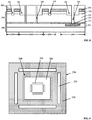
- Figures 6-7 illustrate a corresponding structure; and Figure 7 is a top view of the mark region illustrated in Figure 6 .
- a first mark (not labeled) is formed in the dielectric layer 220 in the first mark region 250; a mark opening 261 is formed in dielectric layer 220 in the second mark region 260; and a first opening 241 is formed in the dielectric layer 220 in the device region 240.
- the bottom of the first opening 214 and the bottom of the mark opening 261 may be higher than the surface of the device layer 240.
- the mark opening 261 may at least expose a portion of the dielectric layer 220 in the second mark region 260.
- the first mark may include a plurality of the first mark trenches 251.
- the plurality of first mark trenches 215 may be evenly distributed around the second mark region 260.
- the number of the first mark trenches 251 is four.
- the top of each first mark trench 251 may be stripe-shaped. Further, the four first mark trenches 251 may form a quadrangle around the second mark region 260. In one embodiment, the lengths of the four first mark trenches 251 are identical; and the four first mark trenches 251 form a square around the second mark region. Further, the sidewalls of the first mark trenches 251 may be perpendicular to the mask layer 230.
- the first mark, the mark opening 261 and the first opening 241 may be formed by etching through the mask layer 230 and etching a portion of the dielectric layer 220 by a first etching process. Specifically, in one embodiment, the second dielectric layer 223 of the dielectric layer 220 may also be etched through; and the top portion of the first dielectric layer 222 may be etched.
- the first opening 241 may be formed in the dielectric layer 220 in the device region 240.
- the first opening 241 may be used to subsequently form a portion of a conductive structure.
- the bottom of the first opening 241 may be lower than the surface of the dielectric layer 220; and may be higher than the surface of the device layer 210.
- the first opening 241 may be used to form an electrical interconnect layer.
- a second opening may be subsequently formed in the bottom of the first opening 241 to expose the conductive layer 211.
- the second opening may be used to form a conductive via; and the conducive via may be used to electrically interconnect the conductive layer 211 and the electrical interconnect layer.
- the conductive via and the electrical interconnect layer may form an electrical conductive structure.
- the first mark When the first opening 241 is formed, the first mark may be formed in the first mark region simultaneously. Thus, the relative position between the first mark and the first opening 241 may be fixed. When a second opening is subsequently formed in the bottom of the first opening 241, a second mark may also be formed simultaneously. Thus, the offset between the first opening and the second opening may be obtained according to the relative position between the first mark and the second mark. Therefore, the fabrication process may be improved according to the offset.
- the process for forming the first mark trenches 251, the mark opening 261 and the first opening 241 may include forming a first pattern layer 201 exposing portions of the surface of the mask layer 230 corresponding to the first mark trenches 251, the mark opening 261 and the first opening 241 on the mask layer 230; and etching the mask layer 230 and the portion of the dielectric layer 220 by the first etching process using the first pattern layer 201 as an etching mask.
- the first mark trenches 251, the mark opening 261 and the first opening 241 may be formed.
- the first pattern layer 201 may be removed.
- the first pattern layer 201 may be a patterned photoresist layer.
- the process for forming the first pattern layer 201 may include forming a first photoresist film on the surface of the mask layer 230 by a spin-coating process; and exposing, developing and baking the photoresist film.
- the photoresist film may be transferred as the first pattern layer 201.
- the first pattern layer 201 may be formed by a nano-imprint process, or a self-assemble process, etc.
- the first etching process may be a dry etching process, or a wet etching process.
- the first etching process is an anisotropic dry etching process.
- the etching gases of the dry etching process may include carbon fluoride gas, O 2 and a carrier gas, etc.
- the flow rate of the etching gas may be in a range of approximately 50 sccm-1000 sccm.
- the pressure of the etching gas may be in a range of approximately 1 mTorr-50 mTorr.
- the bias voltage of the dry etching process may be in a range of approximately 10 V-80 V.
- the power of the dry etching process may be in a range of approximately 100 W-800 W.
- the temperature of the dry etching process may be in a range of approximately 40°C-200°C.
- the carbon fluoride gas may include one or more of CF 4 , C 3 F 8 , C 4 F 8 , CH 2 F 2 , CH 3 F and CHF 3 , etc.
- the carrier gas may include one or more of Ar, He and N 2 , etc.
- the selectivity of the etching gas may be adjusted.
- the adjustment of the ratio between C and F may enable the first etching process to have a relatively high etching selectivity to the mask layer 230 and the dielectric layer 220.
- the mark opening 261 may be formed in the second mark region 260.
- the second mark region 260 may be used to subsequently form a second mark.
- the second mark may have a fixed relative position with the second opening subsequently formed in the bottom of the first opening 241.
- the second etching process used for forming the second opening may etch the dielectric layer 220 in the bottom of the first opening 241
- the second etching process may have a higher etching rate to the dielectric layer 220 than the etching rate of the first etching process to the dielectric layer 220.
- the etching rate of the second etching process to the mask layer 230 may be reduced.
- the mark opening 261 exposing at least a portion of the dielectric layer 220 may be formed in the second mark region 260.
- the bottom of the mark opening 261 may be lower than the surface of the dielectric layer 220 and higher than the surface of the device layer 210. Further, the mark opening 261 may expose a portion of the dielectric layer 220 in the mark region 260. The area of the exposed portion of the dielectric layer 220 may be greater than the area of the region corresponding to the subsequently formed second mark. Such a geometry may ensure to subsequently form the second mark in the dielectric layer 220 in the bottom of the mark opening 261. In certain other embodiments, the mark opening 261 may expose the entire portion of the dielectric layer 220 in the second mark region 260.
- the top of the mark opening 216 is a square and the length of each side of the square may be in a range of approximately 0.02 ⁇ m-0.03 ⁇ m.
- the length of the side of the square may be approximately 0.025 ⁇ m.
- Figures 8-9 illustrate a corresponding structure; and Figure 9 is a top view of the mark region illustrated in Figure 8 .
- a second opening 242 exposing the device layer 210 is formed in the dielectric layer 220 on the bottom of the first opening 241. Further, a second mark (not labeled) is formed in the dielectric layer 220 on the bottom of the mark opening 261.
- the second mark may include a plurality of second mark trenches 262.
- the plurality of second mark trenches 262 may be uniformly distributed around the central point of the second mark region 260.
- the number of the second mark trenches 262 is four.
- the top of each of the second mark trenches 262 may be stripe-shaped; and the four second mark trenches 262 may be distributed as a quadrangle around the central point of the second mark region 260.
- the lengths of the tops of the four second mark trenches 262 are identical.
- the second mark trenches 262 may form a square.
- the side surfaces of the second mark trenches 262 may be perpendicular to the surface of the device layer 210.
- the second opening 242 may be used to subsequently form a portion of a conductive structure. Specifically, the second opening 242 may be used to form a conductive via. The conductive via may be used to electrically connect the electrical interconnect layer subsequently formed in the first opening 241 with the conductive layer 211.
- the second mark may be formed in the dielectric layer 220 on the bottom of the mark opening 261 simultaneously.
- the second mark and the second opening 242 may have a fixed relative position.
- the offset of the second opening 242 relative to the first opening 241 may be obtained according to the overlay mark measurement between the first mark and the second mark.
- the second mark and the second opening 242 may be formed by etching portions of the dielectric layer 220 on the bottom of the first opening 241 and on the bottom of the mark opening 261 using a second etching process.
- the process for forming the plurality of second mark trenches 262 and the second opening 242 may include forming a second pattern layer 202 exposing portions of the surface of the dielectric layer 220 corresponding to the second mark trenches 262 and the second opening 242 on the surface of the mask layer 230 and a portion of the dielectric layer 220; and etching the portions of the dielectric layer 220 by the second etching process using the second pattern layer 202 as an etching mask.
- the second mark trenches 262 and the second opening 242 may be formed.
- the second pattern layer 202 may be removed.
- the second pattern layer 202 may be a patterned photoresist layer.
- an antireflective layer may be formed on the surface of the mask layer 230 and the dielectric layer 220; and the photoresist layer may be formed on the surface of the antireflective layer.
- the process for forming the patterned photoresist layer may include forming a second photoresist layer on the surfaces of the mask layer 230 and the dielectric layer 220 by a spin-coating process; and exposing, developing and baking the photoresist layer.
- the second photoresist layer may be patterned.
- the second pattern layer 202 may be formed by a nano-imprinting process, or a self-assembly process, etc.
- the second etching process may be a dry etching process, or a wet etching process.
- the second etching process is an anisotropic dry etching process.
- the anisotropic dry etching process may be performed until the surface of the conductive layer 211 is exposed.
- the etching gas of the anisotropic dry etching process may include carbon fluoride gas, O 2 and carrier gas, etc.
- the flow rate of the etching gas may be in a range of approximately 50 sccm-1000 sccm.
- the pressure of the etching gas may be in a range of approximately 1 mTorr-50 mTorr.
- the bias voltage of the anisotropic dry etching process may be in a range of approximately 10 V-800 V.
- the power of the anisotropic dry etching process may be in a range of approximately 100 W-800 W.
- the temperature of the anisotropic dry etching process may be in a range of approximately 40°C-200°C.
- the carbon fluoride gas may include one or more of CF 4 , C 3 F 8 , C 4 F 8 , CH 2 F 2 , CH 3 F and CHF 3 , etc.
- the carrier gas may include one or more of Ar, He, and N 2 , etc.
- the etching selectivity of the etching gas may be adjusted. Because the second etching process may be used to etch the dielectric layer 220 until the surface of the conductive layer 211 is exposed, the etching depth in the dielectric layer caused by the second etching process may be relatively large. Thus, the ratio between carbon and fluoride in the etching gas may need to be adjusted to increase the etching rate of the second etching process to the dielectric layer 220 and to reduce the etching rate of the second etching process to the mask layer 230. That is, the etching rate of the second etching process to the mask layer 230 may be smaller than the etching rate of the first etching process to the mask layer 230.
- the second mark trenches 262 and the second opening 242 may have a fixed relative distance, by measuring the overlay precision between the second mark trenches 262 and the first mark trenches 251, the offset of the second opening 242 relative to the first opening 241 may be obtained. According to such an offset, the fabrication process may be improved.
- an overlay mark measurement may be performed to determine the offset of the second opening 242 relative to the first opening 241. If the offset meet the design requirement, a conductive structure may be formed in the first opening 241 and the second opening 242.
- the process for forming the conductive structure may include forming a conductive material film on the surface of the mask layer 230 and in the first opening 241 and the second opening 242.
- the conductive material film may fill the first opening 241 and the second opening 242.
- a planarization process may be performed until the surface of the dielectric layer 220 is exposed.
- the planarization process may be a chemical mechanical polishing process. After removing the conductive material film higher than the surface of the mask layer 230, the chemical mechanical polishing process may continue until the surface of the dielectric layer 220 is exposed.
- the bottoms of the first mark trenches 251 and the bottoms of the second mark trenches 262 may be both lower than the surface of the dielectric layer 220.
- the first mark trenches 251 and the second mark trenches 262 may still exist; and may be still clear. Accordingly, the overlay precision measurement may be accurate.
- a third pattern layer (not shown) may be formed on the surface of the mask layer 230, the mark opening 216, the first mark trenches 251 and the second mark trenches 262 in the mark region.
- the third pattern layer may expose the device region 240.
- the third pattern layer may be made of a transparent material.
- the conductive structure may be made of Cu; and an electrochemical plating (ECP) process may be used to form the conductive structure.
- ECP electrochemical plating
- the process for forming the conductive material film may include forming a seed layer on the surface of the mask layer 230, and the inner side surfaces of the first opening 241 and the second opening 242; and forming the conductive material film by the ECP process until the first opening 241 and the second opening 242 are filled.
- the seed layer may be made of a conductive material.
- the conductive material may be one or more of Cu, W, Al, Ag, Ti, Ta, TiN, and TaN, etc.
- the seed layer may be used as a conductive layer for the ECP process. Further, the seed layer may also be used as a barrier layer between the conductive structure and the dielectric layer 220 to prevent the metal atoms in the conductive structure from diffusing into the dielectric layer 220.
- Various processes may be used to form the seed layer, such as a CVD process, a PVD process, or an ALD process, etc.
- a mark structure may be formed by the disclosed methods and processes.
- Figures 8-9 illustrate a corresponding mark structure.
- the mark structure includes a substrate 200 having a device region 240 and a mark region (not labeled).
- the mark region may include a first mark region 250 and a second mark region 260 surrounded by the first mark region 250.
- the mark structure may also include a conductive layer 211 formed in the surface of the substrate 200 in the device region 240; and a dielectric layer 220 formed on the surface of the substrate 200 and the surface of the conductive layer 211.
- the mark structure may also include a plurality of first mark trenches 251 formed in the dielectric layer 220 in the first mark region 250; and a mark opening 261 and a plurality of second mark trenches 262 formed in the dielectric layer 220 in the second mark region 260.
- the mark structure may also include a conducive structure (not shown) formed in a first opening 241 and a second opening 242 in the dielectric layer 220 in the device region 240.
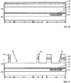
- Figures 10-14 illustrate structures corresponding to certain stages of another exemplary fabrication process of a mark structure consistent with the disclosed embodiments.
- a substrate 300 is provided.
- the substrate 300 may include a mark region (not labeled) and a device region 340.
- the mark region may include a first mark region 350 and a second mark region 360.
- the first mark region 350 may surround the second mark region 360.
- the substrate 300 may include a device layer 310; and a conductive layer 311 may be formed in the surface of the device layer 310 in the device region 340. Further, a dielectric layer 320 may be formed on the surface of the device layer 310 and the conductive layer 311. The dielectric layer 320 may include a barrier layer 311 formed on the surface of the device layer 310 and the surface of the conducive layer 311, a first dielectric layer 322 formed on the barrier layer 311 and a second dielectric layer 323 formed on first dielectric layer 322. Further, a mask layer 330 may be formed on the dielectric layer 320. The detailed information of the substrate 300, the dielectric layer 320 and the mask layer 330 may refer to the previous description of the structure illustrated in Figure 5 .
- a first etching process may be used etch portions of the mask layer 220 and the dielectric layer 320 to form a first opening 341 in the device region 340, a first mark (not labeled) in the first mark region 350 and a mark opening 361 in the second mark region 360.
- the bottom of the first opening 341 and the bottom of the mark opening 361 may be higher than the surface of the device layer 310. Further, the mark opening 361 may expose at least a portion of the dielectric layer 320 in the second mark region 360.
- the first mark may include a plurality of first mark protruding parts 351.
- the plurality of first mark protruding parts 351 may be uniformly distributed around the second mark region 360.
- the number of the first mark protruding parts 351 is four.
- the top of each first mark protruding part 351 may be stripe-shaped; and the four first mark protruding parts 351 may form a quadrangle.
- the lengths of the four first mark protruding parts 351 are identical.
- the four first mark protruding parts 351 form a square.
- the side surfaces of the first mark protruding parts 351 may be perpendicular to the surface of the dielectric layer 320.
- the process for forming the first mark protruding parts 351, the mark opening 361 and the first opening 341 may include forming a first pattern layer 301 exposing the surface of the mask layer 330 in the entire second mark region 360 and portions of the surface of the mask layer 330 in the first mark region 350 and the device region 340 and covering the portions of the mask layer 330 corresponding to the first mark protruding parts 351 on surface of the mask layer 330; and etching the mask layer 330 and the portions of the dielectric layer 320 by the first etching process using the first pattern 301 as an etching mask.
- the first mark protruding parts 351, the mark opening 361 and the first opening 341 may be formed.
- the first pattern layer 301 may be removed.
- the first pattern layer 301 may be a patterned photoresist layer. In certain other embodiments, the first pattern layer 301 may be formed by a nano-imprinting process, or a self-assemble process.
- the first etching process may be an anisotropic dry etching process.
- the etching selectivity of the dry etching process may be adjusted so as to enable the first etching process to have a relatively high etching rate to the mask layer 330 and the dielectric layer 320.
- the mark opening 361 maybe formed simultaneously.
- the mark opening 361 may be used to subsequently form a second mark.
- a second opening 342 and a second mark may be formed.
- the second opening 342 may be formed in the dielectric layer 320 on the bottom of the mark opening 361 (as shown in Figure 11 ).
- the second opening 342 may expose the device layer 310.
- the second mark may be formed in the dielectric layer 320 on the bottom of the mark opening 361.
- the second mark may include a plurality of second mark trenches 362.
- the plurality of second mark trenches 362 may be uniformly distributed around the center of the second mark region 360.
- the number of the second mark trenches 362 is four.
- the top of each second mark trench 362 may be stripe-shaped; and the four second mark trenches 362 may form a quadrangle.
- the lengths of the four second mark trenches 362 are identical.
- the four second mark trenches 362 form a square.
- the side surfaces of the second mark trenches 362 may be perpendicular to the surface of the device layer 310.
- the process for forming the second mark trenches 362 and the second opening 342 may include forming a second pattern layer 302 exposing portions of the surface of the dielectric layer 320 corresponding to the second mark trenches 362 and the second opening 342 on the surface of the mask layer 330; and etching the portions of the dielectric layer 320 by a second etching process using the second pattern layer 302 as an etching mask.
- the second mark trenches 362 and the second opening 342 may be formed.
- the second pattern layer 302 may be removed.
- the second pattern layer 302 may be a patterned photoresist layer. In certain other embodiments, the second pattern layer 302 may be formed by a nano-imprinting process, or a self-assemble process.
- the second etching process may be an anisotropic dry etching process.
- the etching rate of the first etching process to the mask layer 330 may be greater than the etching rate of the second etching process to the mark layer 330.
- an overlay mark measurement of the first mark and the second mark may be performed. If the offset of the first opening and the second opening matches the designed requirement, a conducive structure may be formed in the first opening 341 and the second opening 342.
- a mark structure may be formed by the disclosed methods and processes.
- the corresponding mark structure is illustrate in Figures 13-14 .
- the mark structure includes a substrate 300 having a device region 340 and a mark region (not labeled).
- the mark region may include a first mark region 350 and a second mark region 360 surrounded by the first mark region 350.
- the mark structure may also include a conductive layer 311 formed in the surface of the substrate 300 in the device region 340; and a dielectric layer 320 formed on the surface of the substrate 300 and the surface of the conductive layer 311.
- the mark structure may also include a plurality of first mark protruding structures 351 formed in the dielectric layer 320 in the first mark region 350; and a mark opening 361 and a plurality of second mark trenches 362 formed in the dielectric layer 320 in the second mark region 360.
- the mark structure may also include a conductive structure (not shown) formed in a first opening 341 and a second opening 342 in the dielectric layer 320 in the device region 340.
- a first opening may be formed in the device region, but also a first mark may be formed in the first mark region; and a mark opening may be formed in the second mark region simultaneously.
- the first etching process may be used to etch the mask layer, the etching rate of the first etching process to the mask layer may be relatively high.
- the bottom of the first opening may be lower than the surface of the dielectric layer and higher than the surface of the device layer; and the bottom of the mark opening may also be lower than the surface of the dielectric layer and higher than the surface of the device layer.
- the mark opening may open a process window for subsequently forming a second mark in the second mark region.
- the second etching process may be used to etch the dielectric layer on the bottom of the first opening to expose the surface of the device layer, the etching rate of the second etching process to the dielectric layer may be relative large, but the etching rate of the second etching process to the mask layer may be relatively small. Because the mark opening in the second mark region may also expose a portion of the dielectric layer, the second etching process may be able to etch the dielectric layer in the mark region with an enough depth; and the patterns of the second mark may be clear. Thus, using the first mark and the second mark to perform an overlay mark measurement may be able to accurately obtain the relative offset between the first opening and the second opening. Accordingly, an auxiliary method may be provided to improve the fabrication processes of semiconductor devices.
Landscapes
- Physics & Mathematics (AREA)
- General Physics & Mathematics (AREA)
- Engineering & Computer Science (AREA)
- Multimedia (AREA)
- Internal Circuitry In Semiconductor Integrated Circuit Devices (AREA)
- Geometry (AREA)
- Exposure And Positioning Against Photoresist Photosensitive Materials (AREA)
Abstract
Description
- This application claims the priority of Chinese patent application No.
201610079408.1, filed on February 03, 2016 - The present invention generally relates to the field of semiconductor manufacturing technology and, more particularly, relates to mark structures and fabrication processes thereof.
- During a semiconductor fabrication process, before forming semiconductor devices on a wafer, a layout design of the wafer is necessary to divide the wafer into a plurality of dies and a plurality of scribe lanes among adjacent dies. The dies are used to subsequently form the semiconductor devices; and the scribe lanes are used as cutting lines when the dies are packaged after forming the semiconductor devices.
- Dividing the surface of the wafer into the dies and scribe lanes is often achieved by transferring patterns on a mask of a photolithography process to the surface of the wafer. Specifically, the process for dividing the surface of the wafer into the dies and the scribe lanes includes forming a photoresist layer on the surface of the wafer by a spin-coating process; installing the wafer having the photoresist layer into an exposure apparatus after baking the photoresist layer; exposing the baked photoresist to transfer the patterns on the mask to the photoresist layer by an exposure process; post-baking the exposed photoresist layer; and developing the post-baked photoresist layer to form the patterns in the photoresist layer. In the design of the mask for dividing the surface of the wafer into the dies and the scribe lanes, it is common to form the required patterns of the photolithography process, such as alignment marks and overlay marks, etc., in the scribe lanes.
- For the existing techniques, the photoresist often has offset, rotation, shrinking and extending, and/or orthogonal change, etc., during the overlay exposure process because of the overlay precision, wafer shift and focusing precision, etc. Thus, an overlay measuring mark is required for measuring the exposure error between different dies formed in a same photoresist layer, and/or the exposure error between the dies at a same position of different photoresist layers. By doing so, the overlay precision of the wafer is obtained.
- However, for the overlay marks formed at a same positon of different photoresist layers, there is a resolution difference. Such a resolution difference affects the detection of the overlay precision. Thus, the overlay marks may be unable to meet the requirement of the continuous development of the manufacturing. The disclosed device structures and methods are directed to solve one or more problems set forth above and other problems in the art.
- A first aspect of the present invention provides a method for fabricating a mark structure. The method includes: providing a substrate having a device region and a mark region including a first mark region and a second mark region surrounded by the first mark region; sequentially forming a device layer, a dielectric layer and a mask layer over a surface of the substrate; forming a first opening in the dielectric layer in the device region, a first mark in the dielectric layer in the first mark region, and a mark opening in the dielectric layer in the second mark region, a bottom of the first opening, a bottom of the first mark and a bottom of the mark opening being lower than a surface of the dielectric layer and higher than a surface of the device layer; forming a second opening exposing the device layer in the dielectric layer on the bottom of the first opening and a second mark in the dielectric layer on the bottom of the mark opening; and forming a conductive structure in the first opening and the second opening.
- In one particular embodiment, the first mark includes a plurality of first mark trenches. Preferably, forming the first mark, the first opening, and the first mark opening comprises: forming a first pattern layer exposing portions of a surface of the mask layer corresponding to the first mark trenches, the first opening, and the mark opening on the surface of the mask layer; etching the mask layer and portions of the dielectric layer by a first etching process using the first pattern layer as an etching mask; and removing the first pattern layer.
- Alternatively, the first mark includes a plurality of first mark protruding parts. Preferably, forming the first mark, the first opening, and the first mark opening comprises: forming a first pattern layer exposing an entire portion of a surface of the mask layer in the second mark region and portions of the surface of the mask layer in the device region and the first mark region, and covering a portion of the surface of the mask layer corresponding to the first mark protruding parts on the surface of the mask layer; etching the mask layer and portions of the dielectric layer by a first etching process using the first pattern layer as an etching mask; and removing the first pattern layer.
- In both alternatives above, the second mark preferably includes a plurality of second mark trenches. Forming the second mark and the second opening may further comprise: forming a second pattern layer exposing portions of a surface of the dielectric layer corresponding to the second mark trenches and the second opening on the mask layer; etching the dielectric layer by a second etching process using the second pattern layer as an etching mask; and removing the second pattern layer; wherein preferably: an etching rate of the first etching process to the mask layer is greater than an etching rate of the second etching process to the mask layer.
- A second aspect of the present invention provides a mark structure. The mask structure includes a substrate having a device region and a mark region including a first mark region and a second mark region surrounded by the first mark region; a device layer formed on a surface of the substrate; a dielectric layer formed on a surface of the device layer; a plurality of first marks formed in the dielectric layer in the first mark region; a plurality of second marks formed in the dielectric layer in the second mark region; and a conductive structure electrically connected with the device layer formed in in the dielectric layer in the device region.
- Preferably, the conductive structure further comprises: a mask layer on a surface of the dielectric layer; a first opening in the dielectric layer in the device region, the plurality of the first marks in the dielectric layer in the first mark region, and a mark opening in dielectric layer in the second mark region, a bottom of the first opening, a bottom of the first marks and a bottom of the mark opening being lower than the surface of the dielectric layer, and higher than a surface of the device layer; a second opening exposing the device layer in the dielectric layer on the bottom of the first opening and the plurality of second marks in the dielectric layer on the bottom of the mark opening; and a conductive material in the first opening and the second opening.
- Preferably, the plurality of first marks are uniformly distributed around the second mark region.
- Preferably, in the mark structure: a number of the plurality of first marks is four; a top of each first mark is stripe-shaped; and the four first marks are distributed as a quadrangle around the second mark region.
- Preferably, in the mark structure: a number of the plurality of second marks is four; a top of each second mark is stripe-shaped; and the four second marks are distributed as or form a quadrangle around a center of the second mark region.
- Preferably, the dielectric layer comprises: a barrier layer formed on the surface of the device layer; a first dielectric layer formed on a surface of the barrier layer; and a second dielectric layer formed on a surface of the first dielectric layer. The barrier layer may be made of an N-containing material. The first dielectric layer may be made of a ultra-low-K dielectric material. The second dielectric layer may be made of tetraethyl orthosilicate.
- In all embodiments, the first marks may be first mark protruding parts or, alternatively, the first marks may be first mark trenches. Preferably, the second marks are second mark trenches.
- In the case, wherein the first marks are mark protruding parts and the second marks are mark trenches, preferably: the mark opening covers the entire second mark region; and side surfaces of the mark opening are side surfaces of the first marks.
- A mark structure according to the second aspect of the present invention is obtainable by a method of the first aspect of the present invention.
- Other aspects of the present invention can be understood by those skilled in the art in light of the description, the claims, and the drawings of the present invention.
-
-
Figures 1-4 illustrate structures corresponding to certain stages of an existing fabrication process of an overlay mark; -
Figures 5-9 illustrate structures corresponding to certain stages of an exemplary fabrication process of a mark structure consistent with the disclosed embodiments; -
Figures 10-14 illustrate structures corresponding to certain stages of another exemplary fabrication process of a mark structure consistent with the disclosed embodiments; and -
Figure 15 illustrates an exemplary fabrication process of a mark structure consistent with the disclosed embodiments. - Reference will now be made in detail to exemplary embodiments of the invention, which are illustrated in the accompanying drawings. Wherever possible, the same reference numbers will be used throughout the drawings to refer to the same or like parts.
-
Figures 1-4 illustrate structures corresponding to certain stages of an existing fabrication process of an overlay mark structure. As shown inFigure 1 , the fabrication process includes providing asubstrate 100. Thesubstrate 100 includes amark region 110 and adevice region 120. Adevice layer 101 is formed on the surface of thesubstrate 100 in thedevice region 120; and adielectric layer 102 is formed on the surface of thedevice layer 101 and the surface of thesubstrate 100. Further, amask layer 103 is formed on the surface of thedielectric layer 102. - Further, as shown in
Figure 2 , afirst opening 121 is formed in thedevice region 120 and a plurality offirst mark trenches 111 are formed in themark region 110 by etching themask layer 103 and thedielectric layer 102. The number of thefirst mark trenches 111 is four; and the fourfirst mark trenches 111 form a quadrangle. - Further, as shown in
Figures 3-4 (Figure 4 is a top view of the structure illustrated inFigure 3 ). A plurality of thesecond mark trenches 112 are formed in the region enclosed by the plurality offirst mark trenches 111; and asecond opening 122 is formed on the bottom of thefirst opening 121. Thesecond opening 122 exposes thedevice layer 101. The plurality ofsecond mark trenches 122 and thesecond opening 122 are formed by etching themask layer 103 in themark region 110 and the bottom of thefirst opening 121 using a second etching process. - The
first mark trenches 111 and thesecond mark trenches 112 form an overlay mark structure. Thefirst mark trenches 111 are used to define the position of thefirst opening 121; and thesecond mark trenches 112 are used to define the positon of thesecond opening 122. By measuring the relative positions between thefirst mark trenches 111 and thesecond mark trenches 112, the offset between thefirst opening 121 and thesecond opening 122 is obtained. The fabrication process can be improved according to the obtained offset. - The
first opening 121 and thesecond opening 122 are used to form a conductive structure used to electrically connect with theconductive layer 101; and the process for forming the conductive structure is applicable to form structures with a relatively small feature size. Because thesecond opening 122 needs to expose the surface of thedevice layer 101 to achieve an electrical connection between the conductive structure and thedevice layer 101, thefirst opening 101 needs to be aligned with thedevice layer 101; and thesecond opening 122 also needs to be aligned with theconductive layer 101. - However, after the first etching process or the second etching process, it is easy to induce a stress-releasing between the
mask layer 103 and thedielectric layer 102, and/or between thedielectric layer 102 and thedevice layer 101. Thus, an offset between the position of thefirst opening 121 and the position of thefirst trenches 111 is generated. Accordingly, the positon of the subsequently formedsecond opening 122 relative to thefirst opening 121 and/or thedevice layer 121 is not accurate. - Further, because the
first opening 121 is formed firstly; and the bottom of thefirst opening 121 does not expose thedevice layer 101, the position of thesecond opening 122 needs to be determined by thefirst opening 121. Once thefirst opening 121 has an offset relative to thedevice layer 101, thesecond opening 122 would have a larger offset relative to thedevice layer 101 if thesecond opening 122 has an offset relative to thefirst opening 121. Such a larger offset easily causes the bottom of thesecond opening 122 not to be able to precisely expose thedevice layer 101. Thus, during the fabrication of the conductive layer, it is not allowable to have gradual offsets among thedevice layer 101, thesecond opening 122 and thefirst opening 121 along one direction. - To ensure the position of the
second opening 122 relative to thefirst opening 121 and thedevice layer 101 to be more accurate during the fabrication of the conducive structure, the fabrication process needs to be adjusted according to the overlay precision. Specifically, the fabrication process is improved by accurately measuring the offset of the relative position between thefirst opening 121 and thesecond opening 122; and by learning the offset situation of the relative position between thefirst opening 121 and thesecond opening 122. Thus, the detection of the overlay precision between thefirst opening 121 and thesecond opening 122 has higher requirements. - The first etching process is used to etch the
mask layer 103 and a portion of thedielectric layer 102 to form thefirst opening 121. Thus, the first etching process has a relatively large etching rate to both themask layer 103 and thedielectric layer 102. Accordingly, the depth of thefirst mark trenches 111 is relatively large; and the bottom of thefirst mark trenches 111 is lower than the surface of thedielectric layer 102. However, because the second etching process is used to etch thedielectric layer 102 on the bottom of thefirst opening 121, the second etching process has a larger etching rate to thedielectric layer 102 than to themask layer 103. Such an etching rate difference causes the depth of thesecond mark trenches 112 formed on themark region 110 is relatively small; or even is unable to penetrate throughmask layer 103 to expose thedielectric layer 102. Thus, the patterns of thesecond mark trenches 112 are blurry. Especially after subsequently removing themask layer 103 by a chemical mechanical polishing process, thesecond mark trenches 112 are completely removed; and the overlay precision between thefirst mark trenches 111 and thesecond mark trenches 112 may not be measured. Thus, the fabrication process of the devices is affected. - The present disclosure provides an improved fabrication process of a mark structure.
Figure 15 illustrates an exemplary fabrication process of a mark structure consistent with the disclosed embodiments; andFigures 5-9 illustrate structures corresponding to certain stages of the exemplary fabrication process. - As shown in
Figure 15 , at the beginning of the fabrication process, a substrate with certain structures is provided (S101).Figure 5 illustrates a corresponding structure. - As shown in
Figure 5 , asubstrate 200 is provided. Thesubstrate 200 may include a mark region (not labeled) and adevice region 240. The mark region may include afirst mark region 250 and asecond mark region 260. Thefirst mark region 250 may surround thesecond mark region 260. - Further, a
device layer 210 may be formed on the surface of thesubstrate 200. Adielectric layer 220 may be formed on the surface of thedevice layer 210. Amask layer 230 may be formed on the surface of thedielectric layer 220. - The
device layer 210 may have aconductive layer 211 formed in its surface in thedevice region 240. Thedielectric layer 220 may include abarrier layer 221 formed on the surface of thedevice layer 210; a firstdielectric layer 222 formed on the surface of thebarrier layer 221; and asecond dielectric layer 223 formed on the surface of thesecond dielectric layer 222. - The mark region may be used to form an overlay mark structure. The overlay mark structure may be used to detect the relative offset between the subsequently formed first opening and second opening. The
device region 240 may be used to form semiconductor devices; and the semiconductor devices may form chip circuits, etc. - Further, the
substrate 200 may also include dies (not shown) and scribe lanes (not shown) among adjacent dies distributed as an array. The dies may be used to form individual chips. The scribe lanes may be used to subsequently cut thesubstrate 200. By cutting through the scribe lanes, the plurality of dies may be independent to each other; and the individual chips may be formed. - Further, the
device region 240 may be disposed in a die; and the mark region may be disposed in the scribe lane. After subsequently forming the overlay mark structure in the scribe lanes, when the scribe lanes are cut through, the overlay mark structure may be removed. - In one embodiment, the
substrate 200 may include a base substrate (not shown). Thedevice layer 210 may be formed on the surface of the base substrate. Theconductive layer 211 may be exposed on the surface of thedevice layer 210. - The base substrate may be a Si substrate, a SiGe substrate, a SiC substrate, a silicon-on-insulator (SOI) substrate, a germanium-on-insulator (GOI) substrate, a glass substrate, or a III-V compound substrate (such as GaN, or GaAs), etc.
- The
device layer 210 may include device structures on the surface of the base substrate. The device structures may include one or more of gate structures of the transistors, fuse structures, resistors, capacitors, and inductors, etc. - The
device layer 210 may also include an insulation layer (not shown). The insulation layer may be formed on the surface of the base substrate; and may cover the device structures. The insulation layer may be made of one or more of silicon oxide, silicon nitride, silicon oxynitride, low-K dielectric material, and ultra-low-K material, etc. - Further, the
device layer 210 may also include electrical interconnect structures. The electrical interconnect structures may be formed on the surface of the base substrate and/or the surfaces of the device structures. The electrical interconnect structures may be used to electrically interconnect the device structures and/or electrically interconnect the device structures and the base substrate. The electrical interconnect structures may be made of metal or metal compound, such as one or more of Cu, W, Al, Ti, Ni, TiN, and TaN, etc. The electrical interconnect structure may include conductive vias (or plugs) formed on the surface of the base substrate and/or the surfaces of the devices structures; and theconductive layer 211 formed on the top surface of the conductive vias. Theconductive layer 211 may be used to electrically connect the conductive vias. The consecutive vias and theconductive layer 211 may be distributed in a single layer, or different layers. - In certain other embodiments, the substrate is the base substrate. A conductive layer may be formed in the substrate; and the conductive layer is exposed on the surface of the substrate. The conductive layer may be formed on the surface of an ion-doped region; and the conductive structure may be subsequently formed on the surface of the conductive layer to apply a bias voltage on the ion-doped region. Further, the conductive layer may also be able to connect with through silicon vias (TSV).
- Referring to
Figure 5 , thedielectric layer 220 may include abarrier layer 221, a firstdielectric layer 222 and asecond dielectric layer 223. Thebarrier layer 223 may be made of an N-containing material, etc. Thefirst dielectric layer 222 may be made of an ultra-low-K dielectric material, etc. The dielectric constant of the ultra-low-K dielectric material may be smaller than approximately 2.5. Thesecond dielectric layer 223 may be made of tetraethyl orthosilicate (TEOS), etc. Themask layer 230 may be made of TiN, etc. - The
barrier layer 221 may be made of a material different from that of thefirst dielectric layer 222. Thus, thebarrier layer 221 and thefirst dielectric layer 222 may have an etching selectivity. Accordingly, thebarrier layer 221 may be used as an etching stop layer for a subsequent etching process. - Further, the
first dielectric layer 222 may be made of an ultra-low-K material. The ultra-low-K material may be a porous material. Thus, the external contaminations and water vapor may be easy to penetrate through thefirst dielectric layer 222 to etch the interconnect structures. Therefore, it may need to form thebarrier layer 221 on the surface of thedevice layer 210 before forming thefirst dielectric layer 222. The density of thebarrier layer 221 may be greater than the density of the firstdielectric material layer 222. Thus, thebarrier layer 221 may be able to prevent the external contaminations and water vapor from directly contacting with thedevice layer 210. - The
barrier layer 221 may be made of silicon nitride, or silicon oxynitride, etc. In one embodiment, thebarrier layer 221 is made of silicon oxynitride. The thickness of thebarrier layer 221 may be in a range of approximately 200Å-500Å. Various processes may be used to form thebarrier layer 221, such as a chemical vapor deposition (CVD) process or an atomic layer deposition (ALD) process, etc. - The
first dielectric layer 222 may be made of an ultra-low-K dielectric material. The process for forming the ultra-low-K dielectric material may include forming a seed layer on the surface of thebarrier layer 221; and forming a bulk dielectric layer on the surface of the seed layer. - The seed layer may be made of SiCO, etc. The bulk dielectric layer may be made of porous SiCOH based on the seed layer made of SiCO.
- The hardness and the density of the
second dielectric layer 223 may be greater than those of thefirst dielectric layer 222. Thesecond dielectric layer 223 may be used as an intermediate layer between thefirst dielectric layer 222 and themask layer 230; and may be used to increase the adhesion strength between themask layer 230 and thefirst dielectric layer 222. Further, thesecond dielectric layer 223 may keep a stable morphology during the subsequent planarization process for removing themask layer 230; and may prevent the planarization process from excessively damaging the surface of thedielectric layer 220. - Various processes may be used to form the
second dielectric layer 223. In one embodiment, a CVD process is used to form thesecond dielectric layer 223. The precursor of the CVD process may be TEOS, etc. A TEOS layer may be formed on the surface of thefirst dielectric layer 222. Then, the TEOS layer may be oxidized in an oxygen-containing environment; and silicon oxide may be formed. - The
mask layer 230 may be used as a hard mask layer for subsequently etching thedielectric layer 220 in thedevice region 240 to form a first opening. In one embodiment, themask layer 230 is made of TiN. In certain other embodiments, themask layer 230 may be made of one or more of TaN, Ta, and Ti, etc. Various processes may be used to form themask layer 230, such as a CVD process, an ALD process, or a physical vapor deposition (PVD) process, etc. - In one embodiment, before forming the
mask layer 230, an interface layer may be formed on the surface of thedielectric layer 220. The interface layer may be made of silicon oxide. The interface layer may be used to increase the adhesion strength between themask layer 230 and thedielectric layer 220. - Returning to
Figure 15 , after forming themask layer 230, a first mark, a mark opening and a first opening may be formed (S102).Figures 6-7 illustrate a corresponding structure; andFigure 7 is a top view of the mark region illustrated inFigure 6 . - As shown in
Figures 6-7 , a first mark (not labeled) is formed in thedielectric layer 220 in thefirst mark region 250; amark opening 261 is formed indielectric layer 220 in thesecond mark region 260; and afirst opening 241 is formed in thedielectric layer 220 in thedevice region 240. The bottom of the first opening 214 and the bottom of themark opening 261 may be higher than the surface of thedevice layer 240. Themark opening 261 may at least expose a portion of thedielectric layer 220 in thesecond mark region 260. - The first mark may include a plurality of the
first mark trenches 251. The plurality of first mark trenches 215 may be evenly distributed around thesecond mark region 260. - In one embodiment, the number of the
first mark trenches 251 is four. The top of eachfirst mark trench 251 may be stripe-shaped. Further, the fourfirst mark trenches 251 may form a quadrangle around thesecond mark region 260. In one embodiment, the lengths of the fourfirst mark trenches 251 are identical; and the fourfirst mark trenches 251 form a square around the second mark region. Further, the sidewalls of thefirst mark trenches 251 may be perpendicular to themask layer 230. - The first mark, the
mark opening 261 and thefirst opening 241 may be formed by etching through themask layer 230 and etching a portion of thedielectric layer 220 by a first etching process. Specifically, in one embodiment, thesecond dielectric layer 223 of thedielectric layer 220 may also be etched through; and the top portion of thefirst dielectric layer 222 may be etched. - The
first opening 241 may be formed in thedielectric layer 220 in thedevice region 240. Thefirst opening 241 may be used to subsequently form a portion of a conductive structure. The bottom of thefirst opening 241 may be lower than the surface of thedielectric layer 220; and may be higher than the surface of thedevice layer 210. Thefirst opening 241 may be used to form an electrical interconnect layer. A second opening may be subsequently formed in the bottom of thefirst opening 241 to expose theconductive layer 211. The second opening may be used to form a conductive via; and the conducive via may be used to electrically interconnect theconductive layer 211 and the electrical interconnect layer. The conductive via and the electrical interconnect layer may form an electrical conductive structure. - When the
first opening 241 is formed, the first mark may be formed in the first mark region simultaneously. Thus, the relative position between the first mark and thefirst opening 241 may be fixed. When a second opening is subsequently formed in the bottom of thefirst opening 241, a second mark may also be formed simultaneously. Thus, the offset between the first opening and the second opening may be obtained according to the relative position between the first mark and the second mark. Therefore, the fabrication process may be improved according to the offset. - The process for forming the
first mark trenches 251, themark opening 261 and thefirst opening 241 may include forming afirst pattern layer 201 exposing portions of the surface of themask layer 230 corresponding to thefirst mark trenches 251, themark opening 261 and thefirst opening 241 on themask layer 230; and etching themask layer 230 and the portion of thedielectric layer 220 by the first etching process using thefirst pattern layer 201 as an etching mask. Thus, thefirst mark trenches 251, themark opening 261 and thefirst opening 241 may be formed. After the first etching process, thefirst pattern layer 201 may be removed. - The
first pattern layer 201 may be a patterned photoresist layer. The process for forming thefirst pattern layer 201 may include forming a first photoresist film on the surface of themask layer 230 by a spin-coating process; and exposing, developing and baking the photoresist film. Thus, the photoresist film may be transferred as thefirst pattern layer 201. In certain other embodiments, thefirst pattern layer 201 may be formed by a nano-imprint process, or a self-assemble process, etc. - The first etching process may be a dry etching process, or a wet etching process. In one embodiment, the first etching process is an anisotropic dry etching process. The etching gases of the dry etching process may include carbon fluoride gas, O2 and a carrier gas, etc. The flow rate of the etching gas may be in a range of approximately 50 sccm-1000 sccm. The pressure of the etching gas may be in a range of approximately 1 mTorr-50 mTorr. The bias voltage of the dry etching process may be in a range of approximately 10 V-80 V. The power of the dry etching process may be in a range of approximately 100 W-800 W. The temperature of the dry etching process may be in a range of approximately 40°C-200°C. The carbon fluoride gas may include one or more of CF4, C3F8, C4F8, CH2F2, CH3F and CHF3, etc. The carrier gas may include one or more of Ar, He and N2, etc.
- During the dry etching process, by the adjusting the ratio between C and F, the selectivity of the etching gas may be adjusted. The adjustment of the ratio between C and F may enable the first etching process to have a relatively high etching selectivity to the
mask layer 230 and thedielectric layer 220. - During the first etching process for forming the
first opening 241 in thedevice region 240 and thefirst mark trenches 251 in thefirst mark region 250, themark opening 261 may be formed in thesecond mark region 260. Thesecond mark region 260 may be used to subsequently form a second mark. The second mark may have a fixed relative position with the second opening subsequently formed in the bottom of thefirst opening 241. By measuring the overlay precision between the second mark and the first mark, the offset of the second opening to thefirst opening 241 may be obtained. - Because the subsequent second etching process used for forming the second opening may etch the
dielectric layer 220 in the bottom of thefirst opening 241, the second etching process may have a higher etching rate to thedielectric layer 220 than the etching rate of the first etching process to thedielectric layer 220. The etching rate of the second etching process to themask layer 230 may be reduced. To ensure the subsequent second etching process to be able to form the second mark in thedielectric layer 220, themark opening 261 exposing at least a portion of thedielectric layer 220 may be formed in thesecond mark region 260. - In one embodiment, the bottom of the
mark opening 261 may be lower than the surface of thedielectric layer 220 and higher than the surface of thedevice layer 210. Further, themark opening 261 may expose a portion of thedielectric layer 220 in themark region 260. The area of the exposed portion of thedielectric layer 220 may be greater than the area of the region corresponding to the subsequently formed second mark. Such a geometry may ensure to subsequently form the second mark in thedielectric layer 220 in the bottom of themark opening 261. In certain other embodiments, themark opening 261 may expose the entire portion of thedielectric layer 220 in thesecond mark region 260. - In one embodiment, the top of the mark opening 216 is a square and the length of each side of the square may be in a range of approximately 0.02 µm-0.03 µm. For example, the length of the side of the square may be approximately 0.025 µm.
- Returning to
Figure 15 , after forming the first mark, thefirst mark opening 261 and thefirst opening 241, a second mark and a second opening may be formed (S103).Figures 8-9 illustrate a corresponding structure; andFigure 9 is a top view of the mark region illustrated inFigure 8 . - As shown in
Figures 8-9 , asecond opening 242 exposing thedevice layer 210 is formed in thedielectric layer 220 on the bottom of thefirst opening 241. Further, a second mark (not labeled) is formed in thedielectric layer 220 on the bottom of themark opening 261. - The second mark may include a plurality of
second mark trenches 262. The plurality ofsecond mark trenches 262 may be uniformly distributed around the central point of thesecond mark region 260. - In one embodiment, the number of the
second mark trenches 262 is four. The top of each of thesecond mark trenches 262 may be stripe-shaped; and the foursecond mark trenches 262 may be distributed as a quadrangle around the central point of thesecond mark region 260. - In one embodiment, the lengths of the tops of the four
second mark trenches 262 are identical. Thus, thesecond mark trenches 262 may form a square. Further, the side surfaces of thesecond mark trenches 262 may be perpendicular to the surface of thedevice layer 210. - The
second opening 242 may be used to subsequently form a portion of a conductive structure. Specifically, thesecond opening 242 may be used to form a conductive via. The conductive via may be used to electrically connect the electrical interconnect layer subsequently formed in thefirst opening 241 with theconductive layer 211. - During the process for forming the
second opening 242, the second mark may be formed in thedielectric layer 220 on the bottom of themark opening 261 simultaneously. The second mark and thesecond opening 242 may have a fixed relative position. The offset of thesecond opening 242 relative to thefirst opening 241 may be obtained according to the overlay mark measurement between the first mark and the second mark. - The second mark and the
second opening 242 may be formed by etching portions of thedielectric layer 220 on the bottom of thefirst opening 241 and on the bottom of themark opening 261 using a second etching process. Specifically, the process for forming the plurality ofsecond mark trenches 262 and thesecond opening 242 may include forming asecond pattern layer 202 exposing portions of the surface of thedielectric layer 220 corresponding to thesecond mark trenches 262 and thesecond opening 242 on the surface of themask layer 230 and a portion of thedielectric layer 220; and etching the portions of thedielectric layer 220 by the second etching process using thesecond pattern layer 202 as an etching mask. Thus, thesecond mark trenches 262 and thesecond opening 242 may be formed. After forming thesecond mark trenches 262 and thesecond opening 242, thesecond pattern layer 202 may be removed. - In one embodiment, the
second pattern layer 202 may be a patterned photoresist layer. Before forming the patterned photoresist layer, an antireflective layer may be formed on the surface of themask layer 230 and thedielectric layer 220; and the photoresist layer may be formed on the surface of the antireflective layer. - The process for forming the patterned photoresist layer may include forming a second photoresist layer on the surfaces of the
mask layer 230 and thedielectric layer 220 by a spin-coating process; and exposing, developing and baking the photoresist layer. Thus, the second photoresist layer may be patterned. In certain other embodiments, thesecond pattern layer 202 may be formed by a nano-imprinting process, or a self-assembly process, etc. - The second etching process may be a dry etching process, or a wet etching process. In one embodiment, the second etching process is an anisotropic dry etching process. The anisotropic dry etching process may be performed until the surface of the
conductive layer 211 is exposed. - The etching gas of the anisotropic dry etching process may include carbon fluoride gas, O2 and carrier gas, etc. The flow rate of the etching gas may be in a range of approximately 50 sccm-1000 sccm. The pressure of the etching gas may be in a range of approximately 1 mTorr-50 mTorr. The bias voltage of the anisotropic dry etching process may be in a range of approximately 10 V-800 V. The power of the anisotropic dry etching process may be in a range of approximately 100 W-800 W. The temperature of the anisotropic dry etching process may be in a range of approximately 40°C-200°C. The carbon fluoride gas may include one or more of CF4, C3F8, C4F8, CH2F2, CH3F and CHF3, etc. The carrier gas may include one or more of Ar, He, and N2, etc.
- By adjusting the ratio between carbon and fluoride in the carbon fluoride gas, the etching selectivity of the etching gas may be adjusted. Because the second etching process may be used to etch the
dielectric layer 220 until the surface of theconductive layer 211 is exposed, the etching depth in the dielectric layer caused by the second etching process may be relatively large. Thus, the ratio between carbon and fluoride in the etching gas may need to be adjusted to increase the etching rate of the second etching process to thedielectric layer 220 and to reduce the etching rate of the second etching process to themask layer 230. That is, the etching rate of the second etching process to themask layer 230 may be smaller than the etching rate of the first etching process to themask layer 230. - Because the
second mark trenches 262 and thesecond opening 242 may have a fixed relative distance, by measuring the overlay precision between thesecond mark trenches 262 and thefirst mark trenches 251, the offset of thesecond opening 242 relative to thefirst opening 241 may be obtained. According to such an offset, the fabrication process may be improved. - After forming the second mark, an overlay mark measurement may be performed to determine the offset of the
second opening 242 relative to thefirst opening 241. If the offset meet the design requirement, a conductive structure may be formed in thefirst opening 241 and thesecond opening 242. - The process for forming the conductive structure may include forming a conductive material film on the surface of the
mask layer 230 and in thefirst opening 241 and thesecond opening 242. The conductive material film may fill thefirst opening 241 and thesecond opening 242. After forming the conductive material film, a planarization process may be performed until the surface of thedielectric layer 220 is exposed. - The planarization process may be a chemical mechanical polishing process. After removing the conductive material film higher than the surface of the
mask layer 230, the chemical mechanical polishing process may continue until the surface of thedielectric layer 220 is exposed. - In one embodiment, the bottoms of the
first mark trenches 251 and the bottoms of thesecond mark trenches 262 may be both lower than the surface of thedielectric layer 220. Thus, after the planarization process, thefirst mark trenches 251 and thesecond mark trenches 262 may still exist; and may be still clear. Accordingly, the overlay precision measurement may be accurate. - In one embodiment, before forming the conductive material film, a third pattern layer (not shown) may be formed on the surface of the
mask layer 230, the mark opening 216, thefirst mark trenches 251 and thesecond mark trenches 262 in the mark region. The third pattern layer may expose thedevice region 240. The third pattern layer may be made of a transparent material. - In one embodiment, the conductive structure may be made of Cu; and an electrochemical plating (ECP) process may be used to form the conductive structure. The process for forming the conductive material film may include forming a seed layer on the surface of the
mask layer 230, and the inner side surfaces of thefirst opening 241 and thesecond opening 242; and forming the conductive material film by the ECP process until thefirst opening 241 and thesecond opening 242 are filled. - The seed layer may be made of a conductive material. The conductive material may be one or more of Cu, W, Al, Ag, Ti, Ta, TiN, and TaN, etc. The seed layer may be used as a conductive layer for the ECP process. Further, the seed layer may also be used as a barrier layer between the conductive structure and the
dielectric layer 220 to prevent the metal atoms in the conductive structure from diffusing into thedielectric layer 220. Various processes may be used to form the seed layer, such as a CVD process, a PVD process, or an ALD process, etc. - Thus, a mark structure may be formed by the disclosed methods and processes.
Figures 8-9 illustrate a corresponding mark structure. - As shown
Figures 8-9 , the mark structure includes asubstrate 200 having adevice region 240 and a mark region (not labeled). The mark region may include afirst mark region 250 and asecond mark region 260 surrounded by thefirst mark region 250. The mark structure may also include aconductive layer 211 formed in the surface of thesubstrate 200 in thedevice region 240; and adielectric layer 220 formed on the surface of thesubstrate 200 and the surface of theconductive layer 211. Further, the mark structure may also include a plurality offirst mark trenches 251 formed in thedielectric layer 220 in thefirst mark region 250; and amark opening 261 and a plurality ofsecond mark trenches 262 formed in thedielectric layer 220 in thesecond mark region 260. Further, the mark structure may also include a conducive structure (not shown) formed in afirst opening 241 and asecond opening 242 in thedielectric layer 220 in thedevice region 240. The detailed structures and intermediate structures are described above with respect to the fabrication processes. -
Figures 10-14 illustrate structures corresponding to certain stages of another exemplary fabrication process of a mark structure consistent with the disclosed embodiments. As shown inFigure 10 , at the beginning of the fabrication process, asubstrate 300 is provided. Thesubstrate 300 may include a mark region (not labeled) and adevice region 340. The mark region may include afirst mark region 350 and asecond mark region 360. Thefirst mark region 350 may surround thesecond mark region 360. - The
substrate 300 may include adevice layer 310; and aconductive layer 311 may be formed in the surface of thedevice layer 310 in thedevice region 340. Further, adielectric layer 320 may be formed on the surface of thedevice layer 310 and theconductive layer 311. Thedielectric layer 320 may include abarrier layer 311 formed on the surface of thedevice layer 310 and the surface of theconducive layer 311, a firstdielectric layer 322 formed on thebarrier layer 311 and asecond dielectric layer 323 formed on firstdielectric layer 322. Further, amask layer 330 may be formed on thedielectric layer 320. The detailed information of thesubstrate 300, thedielectric layer 320 and themask layer 330 may refer to the previous description of the structure illustrated inFigure 5 . - Further, as shown in
Figures 11-12 (Figure 12 is a top view of the mark region illustrated inFigure 11 ), after forming themask layer 330, a first etching process may be used etch portions of themask layer 220 and thedielectric layer 320 to form afirst opening 341 in thedevice region 340, a first mark (not labeled) in thefirst mark region 350 and amark opening 361 in thesecond mark region 360. The bottom of thefirst opening 341 and the bottom of themark opening 361 may be higher than the surface of thedevice layer 310. Further, themark opening 361 may expose at least a portion of thedielectric layer 320 in thesecond mark region 360. - The first mark may include a plurality of first
mark protruding parts 351. The plurality of firstmark protruding parts 351 may be uniformly distributed around thesecond mark region 360. - In one embodiment, the number of the first
mark protruding parts 351 is four. The top of each firstmark protruding part 351 may be stripe-shaped; and the four firstmark protruding parts 351 may form a quadrangle. In one embodiment, the lengths of the four firstmark protruding parts 351 are identical. Thus, the four firstmark protruding parts 351 form a square. Further, the side surfaces of the firstmark protruding parts 351 may be perpendicular to the surface of thedielectric layer 320. - The process for forming the first
mark protruding parts 351, themark opening 361 and thefirst opening 341 may include forming afirst pattern layer 301 exposing the surface of themask layer 330 in the entiresecond mark region 360 and portions of the surface of themask layer 330 in thefirst mark region 350 and thedevice region 340 and covering the portions of themask layer 330 corresponding to the firstmark protruding parts 351 on surface of themask layer 330; and etching themask layer 330 and the portions of thedielectric layer 320 by the first etching process using thefirst pattern 301 as an etching mask. Thus, the firstmark protruding parts 351, themark opening 361 and thefirst opening 341 may be formed. After the first etching process, thefirst pattern layer 301 may be removed. - The
first pattern layer 301 may be a patterned photoresist layer. In certain other embodiments, thefirst pattern layer 301 may be formed by a nano-imprinting process, or a self-assemble process. - In one embodiment, the first etching process may be an anisotropic dry etching process. By adjusting the carbon-to-fluoride ratio of the etching gas of the dry etching process, the etching selectivity of the dry etching process may be adjusted so as to enable the first etching process to have a relatively high etching rate to the
mask layer 330 and thedielectric layer 320. - During the first etching process for forming the
first opening 341 and the firstmark protruding structures 351, themark opening 361 maybe formed simultaneously. Themark opening 361 may be used to subsequently form a second mark. - Further, as shown in
Figures 13-14 (Figure 14 is a top view of the mark region illustrated inFigure 13 ), after forming thefirst opening 341, the firstmark protruding structures 351 and themark opening 361, asecond opening 342 and a second mark (not labeled) may be formed. Thesecond opening 342 may be formed in thedielectric layer 320 on the bottom of the mark opening 361 (as shown inFigure 11 ). Thesecond opening 342 may expose thedevice layer 310. - The second mark may be formed in the
dielectric layer 320 on the bottom of themark opening 361. The second mark may include a plurality ofsecond mark trenches 362. The plurality ofsecond mark trenches 362 may be uniformly distributed around the center of thesecond mark region 360. - In one embodiment, the number of the
second mark trenches 362 is four. The top of eachsecond mark trench 362 may be stripe-shaped; and the foursecond mark trenches 362 may form a quadrangle. In one embodiment, the lengths of the foursecond mark trenches 362 are identical. Thus, the foursecond mark trenches 362 form a square. Further, the side surfaces of thesecond mark trenches 362 may be perpendicular to the surface of thedevice layer 310. - The process for forming the
second mark trenches 362 and thesecond opening 342 may include forming asecond pattern layer 302 exposing portions of the surface of thedielectric layer 320 corresponding to thesecond mark trenches 362 and thesecond opening 342 on the surface of themask layer 330; and etching the portions of thedielectric layer 320 by a second etching process using thesecond pattern layer 302 as an etching mask. Thus, thesecond mark trenches 362 and thesecond opening 342 may be formed. After the second etching process, thesecond pattern layer 302 may be removed. - The
second pattern layer 302 may be a patterned photoresist layer. In certain other embodiments, thesecond pattern layer 302 may be formed by a nano-imprinting process, or a self-assemble process. - In one embodiment, the second etching process may be an anisotropic dry etching process. The etching rate of the first etching process to the
mask layer 330 may be greater than the etching rate of the second etching process to themark layer 330. - In one embodiment, after the second etching process, an overlay mark measurement of the first mark and the second mark may be performed. If the offset of the first opening and the second opening matches the designed requirement, a conducive structure may be formed in the
first opening 341 and thesecond opening 342. - Thus, a mark structure may be formed by the disclosed methods and processes. The corresponding mark structure is illustrate in
Figures 13-14 . - As shown
Figures 13-14 , the mark structure includes asubstrate 300 having adevice region 340 and a mark region (not labeled). The mark region may include afirst mark region 350 and asecond mark region 360 surrounded by thefirst mark region 350. The mark structure may also include aconductive layer 311 formed in the surface of thesubstrate 300 in thedevice region 340; and adielectric layer 320 formed on the surface of thesubstrate 300 and the surface of theconductive layer 311. Further, the mark structure may also include a plurality of firstmark protruding structures 351 formed in thedielectric layer 320 in thefirst mark region 350; and amark opening 361 and a plurality ofsecond mark trenches 362 formed in thedielectric layer 320 in thesecond mark region 360. Further, the mark structure may also include a conductive structure (not shown) formed in afirst opening 341 and asecond opening 342 in thedielectric layer 320 in thedevice region 340. The detailed structures and intermediate structures are described above with respect to the fabrication processes. - Therefore, according to the disclosed processes and device structures, during etching the mask layer and the dielectric layer by a first etching process, not only a first opening may be formed in the device region, but also a first mark may be formed in the first mark region; and a mark opening may be formed in the second mark region simultaneously. Because the first etching process may be used to etch the mask layer, the etching rate of the first etching process to the mask layer may be relatively high. Thus, the bottom of the first opening may be lower than the surface of the dielectric layer and higher than the surface of the device layer; and the bottom of the mark opening may also be lower than the surface of the dielectric layer and higher than the surface of the device layer. The mark opening may open a process window for subsequently forming a second mark in the second mark region.
- Further, because the second etching process may be used to etch the dielectric layer on the bottom of the first opening to expose the surface of the device layer, the etching rate of the second etching process to the dielectric layer may be relative large, but the etching rate of the second etching process to the mask layer may be relatively small. Because the mark opening in the second mark region may also expose a portion of the dielectric layer, the second etching process may be able to etch the dielectric layer in the mark region with an enough depth; and the patterns of the second mark may be clear. Thus, using the first mark and the second mark to perform an overlay mark measurement may be able to accurately obtain the relative offset between the first opening and the second opening. Accordingly, an auxiliary method may be provided to improve the fabrication processes of semiconductor devices.
Claims (15)
- A method for forming a mark structure, comprising:providing a substrate having a device region and a mark region including a first mark region and a second mark region surrounded by the first mark region;sequentially forming a device layer, a dielectric layer and a mask layer on a surface of the substrate;forming a first opening in the dielectric layer in the device region, a first mark in the dielectric layer in the first mark region, and a mark opening in dielectric layer in the second mark region, a bottom of the first opening, a bottom of the first mark and a bottom of the mark opening being lower than a surface of the dielectric layer, and higher than a surface of the device layer;forming a second opening exposing the device layer in the dielectric layer on the bottom of the first opening and a second mark in the dielectric layer on the bottom of the mark opening; andforming a conductive structure in the first opening and the second opening.
- The method according to claim 1, wherein:the first mark includes a plurality of first mark trenches.
- The method according to claim 2, wherein forming the first mark, the first opening, and the first mark opening comprises:forming a first pattern layer exposing portions of a surface of the mask layer corresponding to the first mark trenches, the first opening, and the mark opening on the surface of the mask layer;etching the mask layer and portions of the dielectric layer by a first etching process using the first pattern layer as an etching mask; andremoving the first pattern layer.
- The method according to claim 1, wherein:the first mark includes a plurality of first mark protruding parts.
- The method according to claim 4, wherein forming the first mark, the first opening, and the first mark opening comprises:forming a first pattern layer exposing an entire portion of a surface of the mask layer in the second mark region and portions of the surface of the mask layer in the device region and the first mark region, and covering a portion of the surface of the mask layer corresponding to the first mark protruding parts on the surface of the mask layer;etching the mask layer and portions of the dielectric layer by a first etching process using the first pattern layer as an etching mask; andremoving the first pattern layer.
- The method according to any one of the claims 1-5, wherein:the second mark includes a plurality of second mark trenches.
- The method according to claim 6, wherein forming the second mark and the second opening further comprises:forming a second pattern layer exposing portions of a surface of the dielectric layer corresponding to the second mark trenches and the second opening on the mask layer;etching the dielectric layer by a second etching process using the second pattern layer as an etching mask; andremoving the second pattern layer;wherein preferably: an etching rate of the first etching process to the mask layer is greater than an etching rate of the second etching process to the mask layer.
- A mark structure, comprising:a substrate having a device region and a mark region including a first mark region and a second mark region surrounded by the first mark region;a device layer formed on a surface of the substrate;a dielectric layer formed on a surface of the device layer;a plurality of first marks formed in the dielectric layer in the first mark region;a plurality of second marks formed in the dielectric layer in the second mark region; anda conductive structure electrically connected with the device layer formed in in the dielectric layer in the device region.
- The mark structure according to claim 8, wherein the conductive structure further comprises:a mask layer on a surface of the dielectric layer;a first opening in the dielectric layer in the device region, the plurality of the first marks in the dielectric layer in the first mark region, and a mark opening in dielectric layer in the second mark region, a bottom of the first opening, a bottom of the first marks and a bottom of the mark opening being lower than the surface of the dielectric layer, and higher than a surface of the device layer;a second opening exposing the device layer in the dielectric layer on the bottom of the first opening and the plurality of second marks in the dielectric layer on the bottom of the mark opening; anda conductive material in the first opening and the second opening.
- The mark structure according to claim 8 or 9, wherein:the plurality of first marks are uniformly distributed around the second mark region.
- The mark structure according to any one of the claims 8-10, wherein:a number of the plurality of first marks is four;a top of each first mark is stripe-shaped; andthe four first marks are distributed as or form a quadrangle around the second mark region.
- The mark structure according to any one of the claims 8-11, wherein:a number of the plurality of second marks is four;a top of each second mark is stripe-shaped; andthe four second marks are distributed as or form a quadrangle around a center of the second mark region.
- The mark structure according to any one of the claims 8-12, wherein the dielectric layer comprises:a barrier layer formed on the surface of the device layer;a first dielectric layer formed on a surface of the barrier layer; anda second dielectric layer formed on a surface of the first dielectric layer;wherein preferably:the barrier layer is made of an N-containing material;the first dielectric layer is made of a ultra-low-K dielectric material; andthe second dielectric layer is made of tetraethyl orthosilicate.
- The mark structure according to any one of the claims 8-13, wherein:the first marks are first mark protruding parts or, alternatively, the first marks are first mark trenches; andthe second marks are second mark trenches.
- The mark structure according to any one of the claims 8-13, wherein:the first marks are mark protruding parts and the second marks are mark trenches;the mark opening covers the entire second mark region; andside surfaces of the mark opening are side surfaces of the first marks.
Applications Claiming Priority (1)
| Application Number | Priority Date | Filing Date | Title |
|---|---|---|---|
| CN201610079408.1A CN107037699B (en) | 2016-02-03 | 2016-02-03 | Method of forming the marked structure |
Publications (2)
| Publication Number | Publication Date |
|---|---|
| EP3203322A1 true EP3203322A1 (en) | 2017-08-09 |
| EP3203322B1 EP3203322B1 (en) | 2021-09-22 |
Family
ID=57914722
Family Applications (1)
| Application Number | Title | Priority Date | Filing Date |
|---|---|---|---|
| EP17152668.4A Not-in-force EP3203322B1 (en) | 2016-02-03 | 2017-01-23 | Mark structure and fabrication method thereof |
Country Status (3)
| Country | Link |
|---|---|
| US (1) | US9773739B2 (en) |
| EP (1) | EP3203322B1 (en) |
| CN (1) | CN107037699B (en) |
Families Citing this family (17)
| Publication number | Priority date | Publication date | Assignee | Title |
|---|---|---|---|---|
| DE102015122828A1 (en) | 2015-12-23 | 2017-06-29 | Infineon Technologies Austria Ag | A method of manufacturing a semiconductor device having epitaxial layers and an alignment mark |
| JP2017219757A (en) * | 2016-06-09 | 2017-12-14 | ルネサスエレクトロニクス株式会社 | Semiconductor device and manufacturing method thereof |
| CN110034098B (en) * | 2018-01-12 | 2020-11-27 | 中芯国际集成电路制造(上海)有限公司 | Semiconductor structure and method of forming the same |
| CN112635659B (en) * | 2019-10-09 | 2023-03-24 | 中芯国际集成电路制造(上海)有限公司 | Semiconductor structure and forming method thereof |
| CN113517289B (en) * | 2020-04-10 | 2024-02-09 | 长鑫存储技术有限公司 | Semiconductor structure and forming method thereof |
| CN113555345B (en) | 2020-04-23 | 2024-02-06 | 长鑫存储技术有限公司 | Semiconductor mark and forming method thereof |
| TWI730799B (en) * | 2020-06-04 | 2021-06-11 | 力晶積成電子製造股份有限公司 | Method of manufacturing image sensor and alignment mark structure |
| CN114200796B (en) * | 2020-09-02 | 2024-01-26 | 中芯国际集成电路制造(上海)有限公司 | Alignment marks and methods of forming them |
| CN114256204B (en) * | 2020-09-21 | 2025-09-16 | 中芯国际集成电路制造(上海)有限公司 | Semiconductor structure and forming method thereof |
| CN112435936B (en) * | 2020-11-23 | 2022-03-15 | 长江存储科技有限责任公司 | A kind of overlay accuracy detection method and semiconductor structure |
| CN112510016B (en) * | 2020-12-08 | 2024-08-16 | 武汉新芯集成电路股份有限公司 | Semiconductor device and method for manufacturing the same |
| CN113093486B (en) * | 2021-04-15 | 2022-06-28 | 上海交通大学 | Universal alignment mark for electron beam lithography overlay and method of making the same |
| CN113394198A (en) * | 2021-05-28 | 2021-09-14 | 上海华力微电子有限公司 | Photoetching alignment mark and forming method thereof |
| CN115458507B (en) * | 2021-06-09 | 2025-09-16 | 中芯国际集成电路制造(上海)有限公司 | Alignment mark and forming method thereof |
| CN114334822B (en) * | 2021-12-17 | 2025-12-05 | 华虹半导体(无锡)有限公司 | Methods for forming semiconductor structures |
| CN117276048B (en) * | 2022-06-13 | 2026-04-24 | 中芯国际集成电路制造(北京)有限公司 | Semiconductor structure and its formation method |
| CN119560418B (en) * | 2025-01-22 | 2025-06-06 | 荣芯半导体(宁波)有限公司 | Semiconductor structure and manufacturing method thereof |
Citations (3)
| Publication number | Priority date | Publication date | Assignee | Title |
|---|---|---|---|---|
| US20020098707A1 (en) * | 2001-01-24 | 2002-07-25 | Infineon Technologies North America Corp. | Design of lithography alignment and overlay measurement marks on CMP finished damascene surface |
| EP1477860A1 (en) * | 2003-05-12 | 2004-11-17 | ASML Netherlands B.V. | Lithographic marker structure compliant with microelectronic device processing |
| US20120146195A1 (en) * | 2010-12-09 | 2012-06-14 | Hynix Semiconductor Inc. | Overlay vernier mask pattern, formation method thereof, semiconductor device including overlay vernier pattern, and formation method thereof |
Family Cites Families (7)
| Publication number | Priority date | Publication date | Assignee | Title |
|---|---|---|---|---|
| TW388803B (en) * | 1999-03-29 | 2000-05-01 | Nanya Technology Corp | A structure and method of measuring overlapping marks |
| US7192845B2 (en) * | 2004-06-08 | 2007-03-20 | Macronix International Co., Ltd. | Method of reducing alignment measurement errors between device layers |
| US9134627B2 (en) * | 2011-12-16 | 2015-09-15 | Taiwan Semiconductor Manufacturing Company, Ltd. | Multiple-patterning overlay decoupling method |
| CN103630825B (en) * | 2012-08-29 | 2016-01-06 | 中芯国际集成电路制造(上海)有限公司 | Chip test circuit and forming method thereof |
| CN103199084B (en) * | 2013-03-08 | 2015-10-14 | 京东方科技集团股份有限公司 | The manufacture method of substrate alignment mark, substrate and substrate alignment mark |
| US9401332B2 (en) * | 2013-11-22 | 2016-07-26 | Kabushiki Kaisha Toshiba | Method for manufacturing semiconductor device and alignment mark of semiconductor device |
| US9054113B1 (en) * | 2013-12-30 | 2015-06-09 | Nanya Technology Corporation | Box-in-box overlay mark |
-
2016
- 2016-02-03 CN CN201610079408.1A patent/CN107037699B/en active Active
-
2017
- 2017-01-04 US US15/397,788 patent/US9773739B2/en active Active
- 2017-01-23 EP EP17152668.4A patent/EP3203322B1/en not_active Not-in-force
Patent Citations (3)
| Publication number | Priority date | Publication date | Assignee | Title |
|---|---|---|---|---|
| US20020098707A1 (en) * | 2001-01-24 | 2002-07-25 | Infineon Technologies North America Corp. | Design of lithography alignment and overlay measurement marks on CMP finished damascene surface |
| EP1477860A1 (en) * | 2003-05-12 | 2004-11-17 | ASML Netherlands B.V. | Lithographic marker structure compliant with microelectronic device processing |
| US20120146195A1 (en) * | 2010-12-09 | 2012-06-14 | Hynix Semiconductor Inc. | Overlay vernier mask pattern, formation method thereof, semiconductor device including overlay vernier pattern, and formation method thereof |
Also Published As
| Publication number | Publication date |
|---|---|
| CN107037699B (en) | 2019-01-29 |
| US20170221833A1 (en) | 2017-08-03 |
| CN107037699A (en) | 2017-08-11 |
| US9773739B2 (en) | 2017-09-26 |
| EP3203322B1 (en) | 2021-09-22 |
Similar Documents
| Publication | Publication Date | Title |
|---|---|---|
| EP3203322B1 (en) | Mark structure and fabrication method thereof | |
| US10242952B2 (en) | Registration mark formation during sidewall image transfer process | |
| TWI718323B (en) | Semiconductor device having interconnect structure and method of fabricating the same | |
| US8298943B1 (en) | Self aligning via patterning | |
| TWI772691B (en) | Apparatus and method for aligning integrated circuit layers using multiple grating materials | |
| US8585915B2 (en) | Methods for fabricating sub-resolution alignment marks on semiconductor structures | |
| US20170040216A1 (en) | Damascene wires with top via structures | |
| TWI552270B (en) | Semiconductor device and method of manufacturing same | |
| CN106206283B (en) | Trench etching method and first metal layer manufacturing method | |
| CN110690194B (en) | How to make an alignment mark structure | |
| US9646865B1 (en) | Interconnection structure, fabricating method thereof, and exposure alignment system | |
| TWI693675B (en) | Mark structure for aligning layers of integrated circuit structure and methods of forming same | |
| US11031284B2 (en) | Semiconductor device and method of forming the same | |
| KR101056060B1 (en) | Self-aligned contact formation method of vertical transistor and vertical transistor including contact hole | |
| US9117887B2 (en) | Fabrication method of semiconductor device | |
| US9799601B1 (en) | Fuse elements and methods for forming the same | |
| US20080157384A1 (en) | Alignment Key of Semiconductor Device and Method of Manufacturing the Same | |
| US10157796B1 (en) | Forming of marking trenches in structure for multiple patterning lithography | |
| KR20230098237A (en) | Self-Aligned Top Via | |
| US20130299993A1 (en) | Interconnection of semiconductor device and fabrication method thereof |
Legal Events
| Date | Code | Title | Description |
|---|---|---|---|
| PUAI | Public reference made under article 153(3) epc to a published international application that has entered the european phase |
Free format text: ORIGINAL CODE: 0009012 |
|
| STAA | Information on the status of an ep patent application or granted ep patent |
Free format text: STATUS: THE APPLICATION HAS BEEN PUBLISHED |
|
| AK | Designated contracting states |
Kind code of ref document: A1 Designated state(s): AL AT BE BG CH CY CZ DE DK EE ES FI FR GB GR HR HU IE IS IT LI LT LU LV MC MK MT NL NO PL PT RO RS SE SI SK SM TR |
|
| AX | Request for extension of the european patent |
Extension state: BA ME |
|
| STAA | Information on the status of an ep patent application or granted ep patent |
Free format text: STATUS: REQUEST FOR EXAMINATION WAS MADE |
|
| 17P | Request for examination filed |
Effective date: 20180112 |
|
| RBV | Designated contracting states (corrected) |
Designated state(s): AL AT BE BG CH CY CZ DE DK EE ES FI FR GB GR HR HU IE IS IT LI LT LU LV MC MK MT NL NO PL PT RO RS SE SI SK SM TR |
|
| RAP1 | Party data changed (applicant data changed or rights of an application transferred) |
Owner name: SEMICONDUCTOR MANUFACTURING INTERNATIONAL (BEIJING Owner name: SEMICONDUCTOR MANUFACTURING INTERNATIONAL (SHANGHA |
|
| GRAP | Despatch of communication of intention to grant a patent |
Free format text: ORIGINAL CODE: EPIDOSNIGR1 |
|
| STAA | Information on the status of an ep patent application or granted ep patent |
Free format text: STATUS: GRANT OF PATENT IS INTENDED |
|
| INTG | Intention to grant announced |
Effective date: 20210701 |
|
| GRAS | Grant fee paid |
Free format text: ORIGINAL CODE: EPIDOSNIGR3 |
|
| GRAA | (expected) grant |
Free format text: ORIGINAL CODE: 0009210 |
|
| STAA | Information on the status of an ep patent application or granted ep patent |
Free format text: STATUS: THE PATENT HAS BEEN GRANTED |
|
| AK | Designated contracting states |
Kind code of ref document: B1 Designated state(s): AL AT BE BG CH CY CZ DE DK EE ES FI FR GB GR HR HU IE IS IT LI LT LU LV MC MK MT NL NO PL PT RO RS SE SI SK SM TR |
|
| REG | Reference to a national code |
Ref country code: GB Ref legal event code: FG4D |
|
| REG | Reference to a national code |
Ref country code: DE Ref legal event code: R096 Ref document number: 602017046275 Country of ref document: DE |
|
| REG | Reference to a national code |
Ref country code: IE Ref legal event code: FG4D |
|
| REG | Reference to a national code |
Ref country code: CH Ref legal event code: EP Ref country code: AT Ref legal event code: REF Ref document number: 1432788 Country of ref document: AT Kind code of ref document: T Effective date: 20211015 |
|
| REG | Reference to a national code |
Ref country code: LT Ref legal event code: MG9D |
|
| REG | Reference to a national code |
Ref country code: NL Ref legal event code: MP Effective date: 20210922 |
|
| PG25 | Lapsed in a contracting state [announced via postgrant information from national office to epo] |
Ref country code: SE Free format text: LAPSE BECAUSE OF FAILURE TO SUBMIT A TRANSLATION OF THE DESCRIPTION OR TO PAY THE FEE WITHIN THE PRESCRIBED TIME-LIMIT Effective date: 20210922 Ref country code: RS Free format text: LAPSE BECAUSE OF FAILURE TO SUBMIT A TRANSLATION OF THE DESCRIPTION OR TO PAY THE FEE WITHIN THE PRESCRIBED TIME-LIMIT Effective date: 20210922 Ref country code: LT Free format text: LAPSE BECAUSE OF FAILURE TO SUBMIT A TRANSLATION OF THE DESCRIPTION OR TO PAY THE FEE WITHIN THE PRESCRIBED TIME-LIMIT Effective date: 20210922 Ref country code: BG Free format text: LAPSE BECAUSE OF FAILURE TO SUBMIT A TRANSLATION OF THE DESCRIPTION OR TO PAY THE FEE WITHIN THE PRESCRIBED TIME-LIMIT Effective date: 20211222 Ref country code: NO Free format text: LAPSE BECAUSE OF FAILURE TO SUBMIT A TRANSLATION OF THE DESCRIPTION OR TO PAY THE FEE WITHIN THE PRESCRIBED TIME-LIMIT Effective date: 20211222 Ref country code: FI Free format text: LAPSE BECAUSE OF FAILURE TO SUBMIT A TRANSLATION OF THE DESCRIPTION OR TO PAY THE FEE WITHIN THE PRESCRIBED TIME-LIMIT Effective date: 20210922 Ref country code: HR Free format text: LAPSE BECAUSE OF FAILURE TO SUBMIT A TRANSLATION OF THE DESCRIPTION OR TO PAY THE FEE WITHIN THE PRESCRIBED TIME-LIMIT Effective date: 20210922 |
|
| REG | Reference to a national code |
Ref country code: AT Ref legal event code: MK05 Ref document number: 1432788 Country of ref document: AT Kind code of ref document: T Effective date: 20210922 |
|
| PG25 | Lapsed in a contracting state [announced via postgrant information from national office to epo] |
Ref country code: LV Free format text: LAPSE BECAUSE OF FAILURE TO SUBMIT A TRANSLATION OF THE DESCRIPTION OR TO PAY THE FEE WITHIN THE PRESCRIBED TIME-LIMIT Effective date: 20210922 Ref country code: GR Free format text: LAPSE BECAUSE OF FAILURE TO SUBMIT A TRANSLATION OF THE DESCRIPTION OR TO PAY THE FEE WITHIN THE PRESCRIBED TIME-LIMIT Effective date: 20211223 |
|
| PG25 | Lapsed in a contracting state [announced via postgrant information from national office to epo] |
Ref country code: AT Free format text: LAPSE BECAUSE OF FAILURE TO SUBMIT A TRANSLATION OF THE DESCRIPTION OR TO PAY THE FEE WITHIN THE PRESCRIBED TIME-LIMIT Effective date: 20210922 |
|
| PG25 | Lapsed in a contracting state [announced via postgrant information from national office to epo] |
Ref country code: IS Free format text: LAPSE BECAUSE OF FAILURE TO SUBMIT A TRANSLATION OF THE DESCRIPTION OR TO PAY THE FEE WITHIN THE PRESCRIBED TIME-LIMIT Effective date: 20220122 Ref country code: SK Free format text: LAPSE BECAUSE OF FAILURE TO SUBMIT A TRANSLATION OF THE DESCRIPTION OR TO PAY THE FEE WITHIN THE PRESCRIBED TIME-LIMIT Effective date: 20210922 Ref country code: RO Free format text: LAPSE BECAUSE OF FAILURE TO SUBMIT A TRANSLATION OF THE DESCRIPTION OR TO PAY THE FEE WITHIN THE PRESCRIBED TIME-LIMIT Effective date: 20210922 Ref country code: PT Free format text: LAPSE BECAUSE OF FAILURE TO SUBMIT A TRANSLATION OF THE DESCRIPTION OR TO PAY THE FEE WITHIN THE PRESCRIBED TIME-LIMIT Effective date: 20220124 Ref country code: PL Free format text: LAPSE BECAUSE OF FAILURE TO SUBMIT A TRANSLATION OF THE DESCRIPTION OR TO PAY THE FEE WITHIN THE PRESCRIBED TIME-LIMIT Effective date: 20210922 Ref country code: NL Free format text: LAPSE BECAUSE OF FAILURE TO SUBMIT A TRANSLATION OF THE DESCRIPTION OR TO PAY THE FEE WITHIN THE PRESCRIBED TIME-LIMIT Effective date: 20210922 Ref country code: ES Free format text: LAPSE BECAUSE OF FAILURE TO SUBMIT A TRANSLATION OF THE DESCRIPTION OR TO PAY THE FEE WITHIN THE PRESCRIBED TIME-LIMIT Effective date: 20210922 Ref country code: EE Free format text: LAPSE BECAUSE OF FAILURE TO SUBMIT A TRANSLATION OF THE DESCRIPTION OR TO PAY THE FEE WITHIN THE PRESCRIBED TIME-LIMIT Effective date: 20210922 Ref country code: CZ Free format text: LAPSE BECAUSE OF FAILURE TO SUBMIT A TRANSLATION OF THE DESCRIPTION OR TO PAY THE FEE WITHIN THE PRESCRIBED TIME-LIMIT Effective date: 20210922 Ref country code: AL Free format text: LAPSE BECAUSE OF FAILURE TO SUBMIT A TRANSLATION OF THE DESCRIPTION OR TO PAY THE FEE WITHIN THE PRESCRIBED TIME-LIMIT Effective date: 20210922 |
|
| REG | Reference to a national code |
Ref country code: DE Ref legal event code: R097 Ref document number: 602017046275 Country of ref document: DE |
|
| PG25 | Lapsed in a contracting state [announced via postgrant information from national office to epo] |
Ref country code: DK Free format text: LAPSE BECAUSE OF FAILURE TO SUBMIT A TRANSLATION OF THE DESCRIPTION OR TO PAY THE FEE WITHIN THE PRESCRIBED TIME-LIMIT Effective date: 20210922 |
|
| PLBE | No opposition filed within time limit |
Free format text: ORIGINAL CODE: 0009261 |
|
| STAA | Information on the status of an ep patent application or granted ep patent |
Free format text: STATUS: NO OPPOSITION FILED WITHIN TIME LIMIT |
|
| REG | Reference to a national code |
Ref country code: DE Ref legal event code: R119 Ref document number: 602017046275 Country of ref document: DE |
|
| 26N | No opposition filed |
Effective date: 20220623 |
|
| PG25 | Lapsed in a contracting state [announced via postgrant information from national office to epo] |
Ref country code: MC Free format text: LAPSE BECAUSE OF FAILURE TO SUBMIT A TRANSLATION OF THE DESCRIPTION OR TO PAY THE FEE WITHIN THE PRESCRIBED TIME-LIMIT Effective date: 20210922 |
|
| REG | Reference to a national code |
Ref country code: CH Ref legal event code: PL |
|
| GBPC | Gb: european patent ceased through non-payment of renewal fee |
Effective date: 20220123 |
|
| REG | Reference to a national code |
Ref country code: BE Ref legal event code: MM Effective date: 20220131 |
|
| PG25 | Lapsed in a contracting state [announced via postgrant information from national office to epo] |
Ref country code: LU Free format text: LAPSE BECAUSE OF NON-PAYMENT OF DUE FEES Effective date: 20220123 Ref country code: GB Free format text: LAPSE BECAUSE OF NON-PAYMENT OF DUE FEES Effective date: 20220123 Ref country code: DE Free format text: LAPSE BECAUSE OF NON-PAYMENT OF DUE FEES Effective date: 20220802 |
|
| PG25 | Lapsed in a contracting state [announced via postgrant information from national office to epo] |
Ref country code: SI Free format text: LAPSE BECAUSE OF FAILURE TO SUBMIT A TRANSLATION OF THE DESCRIPTION OR TO PAY THE FEE WITHIN THE PRESCRIBED TIME-LIMIT Effective date: 20210922 Ref country code: FR Free format text: LAPSE BECAUSE OF NON-PAYMENT OF DUE FEES Effective date: 20220131 Ref country code: BE Free format text: LAPSE BECAUSE OF NON-PAYMENT OF DUE FEES Effective date: 20220131 |
|
| PG25 | Lapsed in a contracting state [announced via postgrant information from national office to epo] |
Ref country code: LI Free format text: LAPSE BECAUSE OF NON-PAYMENT OF DUE FEES Effective date: 20220131 Ref country code: CH Free format text: LAPSE BECAUSE OF NON-PAYMENT OF DUE FEES Effective date: 20220131 |
|
| PG25 | Lapsed in a contracting state [announced via postgrant information from national office to epo] |
Ref country code: IT Free format text: LAPSE BECAUSE OF FAILURE TO SUBMIT A TRANSLATION OF THE DESCRIPTION OR TO PAY THE FEE WITHIN THE PRESCRIBED TIME-LIMIT Effective date: 20210922 Ref country code: IE Free format text: LAPSE BECAUSE OF NON-PAYMENT OF DUE FEES Effective date: 20220123 |
|
| PG25 | Lapsed in a contracting state [announced via postgrant information from national office to epo] |
Ref country code: HU Free format text: LAPSE BECAUSE OF FAILURE TO SUBMIT A TRANSLATION OF THE DESCRIPTION OR TO PAY THE FEE WITHIN THE PRESCRIBED TIME-LIMIT; INVALID AB INITIO Effective date: 20170123 |
|
| PG25 | Lapsed in a contracting state [announced via postgrant information from national office to epo] |
Ref country code: SM Free format text: LAPSE BECAUSE OF FAILURE TO SUBMIT A TRANSLATION OF THE DESCRIPTION OR TO PAY THE FEE WITHIN THE PRESCRIBED TIME-LIMIT Effective date: 20210922 Ref country code: MK Free format text: LAPSE BECAUSE OF FAILURE TO SUBMIT A TRANSLATION OF THE DESCRIPTION OR TO PAY THE FEE WITHIN THE PRESCRIBED TIME-LIMIT Effective date: 20210922 Ref country code: CY Free format text: LAPSE BECAUSE OF FAILURE TO SUBMIT A TRANSLATION OF THE DESCRIPTION OR TO PAY THE FEE WITHIN THE PRESCRIBED TIME-LIMIT Effective date: 20210922 |
|
| PG25 | Lapsed in a contracting state [announced via postgrant information from national office to epo] |
Ref country code: MT Free format text: LAPSE BECAUSE OF FAILURE TO SUBMIT A TRANSLATION OF THE DESCRIPTION OR TO PAY THE FEE WITHIN THE PRESCRIBED TIME-LIMIT Effective date: 20210922 |
|
| PG25 | Lapsed in a contracting state [announced via postgrant information from national office to epo] |
Ref country code: TR Free format text: LAPSE BECAUSE OF FAILURE TO SUBMIT A TRANSLATION OF THE DESCRIPTION OR TO PAY THE FEE WITHIN THE PRESCRIBED TIME-LIMIT Effective date: 20210922 |