EP3202573A1 - Optoelektronischer sensor mit verfahren zur herstellung - Google Patents
Optoelektronischer sensor mit verfahren zur herstellung Download PDFInfo
- Publication number
- EP3202573A1 EP3202573A1 EP17151450.8A EP17151450A EP3202573A1 EP 3202573 A1 EP3202573 A1 EP 3202573A1 EP 17151450 A EP17151450 A EP 17151450A EP 3202573 A1 EP3202573 A1 EP 3202573A1
- Authority
- EP
- European Patent Office
- Prior art keywords
- optical component
- optical
- printing
- positioning device
- carrier
- Prior art date
- Legal status (The legal status is an assumption and is not a legal conclusion. Google has not performed a legal analysis and makes no representation as to the accuracy of the status listed.)
- Granted
Links
Images

Classifications
-
- G—PHYSICS
- G01—MEASURING; TESTING
- G01V—GEOPHYSICS; GRAVITATIONAL MEASUREMENTS; DETECTING MASSES OR OBJECTS; TAGS
- G01V8/00—Prospecting or detecting by optical means
- G01V8/10—Detecting, e.g. by using light barriers
-
- B—PERFORMING OPERATIONS; TRANSPORTING
- B33—ADDITIVE MANUFACTURING TECHNOLOGY
- B33Y—ADDITIVE MANUFACTURING, i.e. MANUFACTURING OF THREE-DIMENSIONAL [3D] OBJECTS BY ADDITIVE DEPOSITION, ADDITIVE AGGLOMERATION OR ADDITIVE LAYERING, e.g. BY 3D PRINTING, STEREOLITHOGRAPHY OR SELECTIVE LASER SINTERING
- B33Y80/00—Products made by additive manufacturing
Definitions
- the invention relates to a method for producing an optoelectronic sensor and to an optoelectronic sensor according to the preamble of claims 1 and 10, respectively.
- the 3D printing technology is becoming increasingly established for the flexible production of components to any specification. However, it is not yet applicable for optoelectronic sensors. It will be even longer time for the required precision for high-quality optical parts or even optics carriers with sufficiently low tolerances missing. Even that would not guarantee the above mentioned adjustment, because there must continue to be a downstream adjusted composition. With the problem of printing optical precision parts and their holders in combination with each other and with the other components of a sensor, the available 3D printing technology would be completely overburdened.
- optical components are those that contribute to the optical path of the sensor. These are usually several, but the invention is often explained for simplicity only on the basis of a single optical component, without implying any limitation, because the principle can be generalized. It is conceivable not to adjust some of the optical components, because they can do without adjustment or with a very rough adjustment. Similarly, some of the optical components may not be adjusted according to the invention but with another concept, of which some are mentioned in the introduction. In general, six degrees of freedom in position and orientation relative to the housing or relative to one or more other optical components can be considered for the adjustment, but usually only one degree of freedom for a particular optical component is relevant or several, but not all degrees of freedom are relevant.
- the invention is based on the basic idea of initially positioning the optical component freely in space with the aid of a positioning device.
- the optical component is therefore unlike the prior art just not introduced into a predetermined holder and can be adjusted without any restriction.
- an optical carrier is produced around the optical component by means of 3D printing, which fixes the optical component in the already achieved adjustment. This fixation is then permanent and remains in the sensor.
- the optical carrier and the optical component form a common component after completion of 3D printing.
- the optical carrier is printed around the optical component in the sense that both are in proper alignment with each other right after 3D printing. she For example, they are connected to each other or form a common component.
- the production of the optical carrier thus also contains the step with which the optical component is otherwise used in the optical carrier. If the 3D printing makes this possible, the optics carrier can also offer adjustment possibilities, for example several detent positions, the optical component then being in the adjusted setting after production, but this could be varied later.
- the invention has the advantage that a particularly simple and cost-effective production of optoelectronic sensors is made possible.
- Tolerances of the 3D printing play no role, because at the interface to the optical component, the fixation of the positioning ensures accurate adjustment.
- Whether the optics carrier then has a certain play of material on a side remote from the optical component is irrelevant to the function. Because of the free positioning of the optical component in the room independently of other sensor components, virtually any degree of freedom is available for an exact adjustment adapted to the task of the sensor.
- the method according to the invention allows a much faster and easier transition from development to production, and it is particularly suitable for the sample construction and small series or even individual sensors.
- the positioning device is preferably adjusted to adjust the predetermined adjustment of the optical component. In principle, it would also be conceivable to achieve the adjustment via a rigid specification of the positioning device or variations, as the optical component is held in the positioning device. It is simpler if the positioning device itself provides the required degrees of freedom for an adjustment.
- the positioning device is preferably adjusted with its own drive. It is therefore an active positioning, which does not have to be moved by hand, but which can be moved, for example, with a control unit or software to a desired location and / or rotated in a desired orientation.
- the positioning device is preferably operated by a robot or is part of a robot.
- the robot or robot arm enables an automatic process.
- the optical component is removed in an automatic sequence from a storage container and brought into the adjusted 6D position, wherein, as already mentioned above, not all degrees of freedom are generally relevant.
- a sensor function can be active, by means of which the robot tracks the optical component until the sensor function satisfies a specification.
- the positioning device is preferably removed after or during the 3D printing.
- the robot releases as soon as the 3D printing material fixes the optical component in the adjustment.
- a waiting time for curing may be required.
- a further 3D printing step is conceivable in order to complete the production of the optical carrier also over the gripping regions.
- the optical carrier is preferably produced in the 3D printing process as part of a housing or together with a housing. So it's not just an optics carrier printed, but also the case.
- further or all components of the sensor can be held by the positioning device or otherwise in the region of the 3D printing.
- the movement into the predetermined adjustment with the aid of the positioning device and the 3D printing process preferably takes place as a common production step in a production line of the sensor.
- the optical carrier is therefore not prepared in advance, but rather the responsible 3D printer is integrated into the production line, and the adjusted connection of optical carrier and optical component by 3D printing is only a partial step of the final production. This is much faster and more effective.
- the positioning device with the 3D printer is practically a universal station for a wide variety of sensors, because the optical carrier must be set only when starting the 3D printing.
- the optical component is preferably at least part of a light transmitter, a light receiver, a transmission optics or a receiving optics. These are the most important examples for optical components, which may be somewhat more specific lenses, mirrors, diffractive optical elements, apertures and various filters, such as polar or color filters.
- the optical component is preferably provided with connection areas for holding in the positioning device and / or for the optics carrier produced in the 3D printing process. This facilitates handling or a stable connection with the optical component during 3D printing of the optics carrier.
- the optical component can be specified and manufactured directly with the connection regions, for example as an extended lens with connection regions in an injection molding process. However, it is also conceivable to subdivide the 3D printing into two steps, in which first connection regions are printed on the optical component and then only the optical carrier. This can also be done in the same 3D printer. In principle, it is also conceivable to create the optical component including terminal areas in 3D printing, but this would have to overcome the difficulties already mentioned in the introduction, with 3D printing to achieve sufficient precision for a high-quality optical component.
- the sensor according to the invention is characterized in that the predetermined adjustment of the optical component is achieved by an optical carrier which is printed around the optical component in a 3D printing process.
- an optical carrier which is printed around the optical component in a 3D printing process.
- An inventive or inventively manufactured sensor is preferably an industrial sensor, for example a light barrier, a light scanner, in particular a distance-measuring light scanner, a laser scanner, a code reader or a camera in one to three dimensions.
- Such sensors are often used in a stationary assembly for monitoring, for example, a work area or a robot cell, for securing or supporting the process, or on conveyor belts.
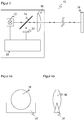
- FIG. 1 shows a schematic representation of an optoelectronic sensor 10.
- a light emitter 12 emits a light signal which passes through a splitter mirror 14 and is then guided by means of a lens 16 to an object 18. After remission or reflection, a portion of the light signal returns, is focused by the lens 16 and deflected by the splitter mirror 14 onto a light receiver 20.
- An evaluation unit 22 is connected to the light transmitter 12 and the light receiver 20. In this way, a desired light signal is generated by means of the light transmitter 12 and the reception signal subsequently generated by the light receiver 20 is evaluated in order, for example, to detect the presence of the object 18.
- the invention is not limited to a particular sensor type or a particular design. Rather, it is only important that at least one optical component is present, which, for correct functioning of the sensor, has an adjusted position and / or orientation relative to the sensor or to another optical component must have.
- These optical components can in the embodiment of the FIG. 1 the light emitter 10, the divider mirror 14, the lens 16 and / or the light receiver 20 may be.
- FIGS. 2 and 3 show the relevant manufacturing steps, with which the optical components are fixed with a 3D-printed optics carrier in the desired adjustment. Not all optical components need to be adjusted in this way. It is also conceivable to adjust some optical components in other ways, and again other optical components may not require adjustment or only a very rough adjustment.
- FIG. 2 shows a first of the respective manufacturing steps, in which two optical components, namely the light emitter 12 and the lens 16, are positioned to each other.
- the optical components are to be understood purely by way of example; likewise, the light receiver 20 could be positioned relative to the lens 16, two or more arbitrary optical components to one another or only one optical component to the optical carrier still to be created.
- the optical components 12, 16 to be aligned with one another are positioned freely in space with the aid of a positioning device 24a-b in such a way that the desired interaction results.
- a positioning device 24a-b In the illustrated example, one optical component 12 is held by a rigid part 24a of the positioning device and only the other optical component 16 is moved. This is then sufficient and simplifies the positioning 24a-b, if it only depends on the relative position of the optical components 12, 16 to each other.
- the solid part 24a may also be replaced to move both optical components 16.
- the movable part 24b of the positioning device is, for example, a robot arm, although other electrically adjustable or mechanical movements are also conceivable.
- the freedom of movement of the movable part 24b in all six degrees of freedom of translation and rotation is symbolized by an axis system 26. Often, only a portion of these degrees of freedom is actually needed, for example, only one degree of translation freedom on the axis between the optical components 12, 16 to adjust the spacing. That's enough then a correspondingly simplified movable part 24b of the positioning device.
- the receptacles of the positioning device 24a-b are very precise, so that it is sufficient to approach a predetermined fixed position.
- a form of feedback will also be incorporated. This can be a comparison with a target position by a camera or an operator. For very accurate alignment results, it is useful to enable the optical path to be set and see if the desired result is achieved.
- the light emitter 12 can be switched on and the light spot behind the lens 16 can be checked.
- the first production step is completed.
- FIG. 3 illustrates the subsequent second manufacturing step.
- the positioning device 24a-b remains in the previously reached position and thus keeps the optical components 12, 16 in the desired orientation.
- a 3D printer not shown, is constructed an optical carrier 28 around the optical components 12, 16, which fixes the optical components 12, 16 in the achieved alignment.
- the stripe pattern in FIG. 3 indicates a layer structure of the 3D printing process on a substrate 30, for example a workbench, but with which no special 3D printing process is to be defined.
- the optical components 12, 16 can be released by the positioning device 24a-b as soon as they are sufficiently fixed. It is conceivable only then complete the 3D printing, if this was previously not possible because of the gripping contact. In this case, there may be waiting times during the 3D printing or after that, so that the material of the optical carrier 28 cools or hardens.
- the 3D printing is not limited to the optical carrier 28 alone, but it can be a larger assembly with the optical carrier 28 or the entire housing to be printed. Of course, more or less than the two optical components 12, 16 shown by way of example may be held in an adjusted position. On the other hand, it is also possible to print only images for those components whose alignment can cope with the tolerances of 3D printing, and to subsequently use these components. Also, non-optical components can be integrated into the 3D printing, for example by connecting an electric motor, the fixation of whole electronic cards or other other sensor components.
- FIG. 4 illustrates a conceivable supporting measure for 3D printing. It is FIG. 4a a front view and FIG. 4b a section of the lens 16 as a naturally replaceable example of an optical component.
- the lens 16 is provided in this embodiment with "ears" or pads 32.
- the terminal areas 32 make it easier for the positioning device 24a-b to grip the lens 16 and fix it in the desired orientation during the 3D printing. In addition, they can provide better interfacing between the lens 16 and the printed optics carrier 28.
- the connection regions 32 can be made in one piece with the lens 16, for instance by injection molding, or the lens 16 is assembled with the connection region 32. In this case, no special precision is required, because it does not depend on the mutual alignment of the lens 16 and connection area 32, but on the effective orientation of the first yes with the help of the positioning device 24a-b freely positionable lens 16.
- the positioning device 24a-b forms, together with the 3D printer, a kind of universal station for the ready-to-use production of a wide variety of completely adjusted optical assemblies.
- a particular advantage is that the manufacturing process according to the invention with positioning and 3D printing can take place directly in the production line. This speeds up the production compared to a conventional, temporally upstream production of an optical carrier 28 quite considerably. In addition, it is very easy and inexpensive to ensure any desired orientation. In addition, the production line becomes highly flexible for a wide variety of sensor variants or even sensor types. This also small and small series or even individually specified sensors are economically produced. In addition, the process is suitable for prototyping and significantly accelerates the development and transition from development to mass production.
Landscapes
- Physics & Mathematics (AREA)
- Life Sciences & Earth Sciences (AREA)
- General Life Sciences & Earth Sciences (AREA)
- General Physics & Mathematics (AREA)
- Geophysics (AREA)
- Chemical & Material Sciences (AREA)
- Engineering & Computer Science (AREA)
- Manufacturing & Machinery (AREA)
- Materials Engineering (AREA)
- Manufacture Of Switches (AREA)
- Switches Operated By Changes In Physical Conditions (AREA)
Abstract
Description
- Die Erfindung betrifft ein Verfahren zur Herstellung eines optoelektronischen Sensors und einen optoelektronischen Sensor nach dem Oberbegriff von Anspruch 1 beziehungsweise 10.
- Für eine reibungslose Funktion muss in optoelektronischen Sensoren zur Erfüllung der jeweiligen Qualitätsanforderungen eine verlässliche Justierung gewährleistet werden. Es ist üblich, die Optikteile in einem eigens spezifizierten und hergestellten Optikträger unterzubringen, der für die gewünschte justierte Position und Orientierung sorgt. Der Optikträger besitzt dann beispielsweise hochgenaue Passflächen zur Aufnahme der Einzelteile. Optikträger wie Optikteile müssen dazu mit entsprechender Fertigungsgenauigkeit hergestellt sein. Alternativ sind händische oder auch automatisierte, dann aber aufwändig auf den speziell zu fertigenden Sensor abgestimmte Justier- und Befestigungsprozesse erforderlich. Eine weitere Lösung besteht darin, Freiheitsgrade im Design vorzusehen, und diese Verstellmöglichkeiten des Sensors werden dann bei der Endmontage oder in einem werkseitigen Kalibrierprozess zur Justierung genutzt. Auch das bindet über das aufwändigere Design mit den Verstellmöglichkeiten hinaus Betriebsmittel beziehungsweise Personalaufwand für die Durchführung. Bei allen diesen herkömmlichen Verfahren werden also durch die Justageanforderungen die Herstellkosten erheblich erhöht.
- Die 3D-Drucktechnik etabliert sich immer stärker für die flexible Herstellung von Bauteilen nach beliebiger Spezifikation. Für optoelektronische Sensoren ist sie aber noch nicht einsetzbar. Es wird noch längere Zeit an der erforderlichen Präzision für hochwertige Optikteile oder auch nur von Optikträgern mit hinreichend geringen Toleranzen fehlen. Selbst das würde die oben angesprochene Justierung noch nicht gewährleisten, weil weiterhin ein nachgelagertes justiertes Zusammensetzen erfolgen muss. Mit der Problemstellung, optische Präzisionsteile und deren Halterungen im Verbund miteinander und mit den übrigen Komponenten eines Sensors zu drucken, wäre nämlich die verfügbare 3D-Drucktechnik erst recht völlig überfordert.
- Es ist daher Aufgabe der Erfindung, die Fertigung von Sensoren unter Beachtung von Justageanforderungen an dessen optische Komponenten zu vereinfachen.
- Diese Aufgabe wird durch ein Verfahren zur Herstellung eines optoelektronischen Sensors und durch einen optoelektronischen Sensor nach Anspruch 1 beziehungsweise 10 gelöst. Mit dem Verfahren wird ein optoelektronischer Sensor hergestellt, dessen optische Komponenten eine geforderte Justage aufweisen. Die optischen Komponenten sind diejenigen, die zum optischen Pfad des Sensors beitragen. Das sind meist mehrere, aber die Erfindung wird zur Vereinfachung häufig nur anhand einer einzigen optischen Komponente erläutert, ohne damit eine Einschränkung zu implizieren, weil sich das Prinzip verallgemeinern lässt. Es ist denkbar, einige der optischen Komponenten nicht zu justieren, weil sie auch ohne Justierung oder mit einer nur sehr groben Justierung auskommen. Ebenso können einige der optischen Komponenten nicht gemäß der Erfindung, sondern mit einem anderen Konzept justiert werden, von denen einleitend einige genannt sind. Allgemein können für die Justierung sechs Freiheitsgrade in Lage und Orientierung gegenüber dem Gehäuse beziehungsweise relativ zu einem oder mehreren anderen optischen Komponenten berücksichtigt werden, wobei aber meist nur ein Freiheitsgrad für eine bestimmte optische Komponente relevant ist beziehungsweise mehrere, aber nicht alle Freiheitsgrade relevant sind.
- Die Erfindung geht nun von dem Grundgedanken aus, die optische Komponente zunächst mit Hilfe einer Positioniereinrichtung frei im Raum zu positionieren. Die optische Komponente ist also anders als im Stand der Technik gerade nicht in eine vorgegebene Halterung eingebracht und kann so ohne jede Beschränkung justiert werden. Wenn das erreicht ist, wird um die optische Komponente herum mittels 3D-Druck ein Optikträger hergestellt, der die optische Komponente in der bereits erreichten Justierung fixiert. Diese Fixierung ist dann dauerhaft und bleibt im Sensor erhalten. Der Optikträger und die optische Komponente bilden nach vollendetem 3D-Druck ein gemeinsames Bauteil. Der Optikträger ist in dem Sinne um die optische Komponente gedruckt, dass beide direkt nach dem 3D-Druck in der richtigen Justierung zueinander stehen. Sie sind beispielsweise miteinander verbunden oder bilden ein gemeinsames Bauteil. Die Herstellung des Optikträgers enthält also zugleich den Schritt, mit dem sonst die optische Komponente in den Optikträger eingesetzt wird. Sofern der 3D-Druck das leistet, kann der Optikträger auch Verstellmöglichkeiten bieten, beispielsweise mehrere Rastpositionen, wobei sich dann nach der Herstellung die optische Komponente in der justierten Einstellung befindet, diese aber später variiert werden könnte.
- Die Erfindung hat den Vorteil, dass eine besonders einfache und kostengünstige Herstellung von optoelektronischen Sensoren ermöglicht wird. Es erfolgt eine funktionsfertige Herstellung von Optikbaugruppen und ganzen Sensoren. Eine Herstellung von spezifizierten Optikträgern mit besonderen, meist sehr teuren Werkzeugen, etwa Spritzgusswerkzeugen, ist nicht erforderlich. Toleranzen des 3D-Drucks spielen keine Rolle, weil an der Schnittstelle zur optischen Komponente die Fixierung der Positioniereinrichtung für eine genaue Justierung sorgt. Ob dann der Optikträger an einer von der optischen Komponente abgewandten Seite ein gewisses Materialspiel aufweist, ist für die Funktion belanglos. Wegen der freien Positionierung der optischen Komponente im Raum unabhängig von anderen Sensorbauteilen stehen praktisch beliebige Freiheitsgrade für eine exakte, an die Aufgabe des Sensors angepasste Justierung zur Verfügung. Das erfindungsgemäße Verfahren erlaubt einen deutlich schnelleren und vereinfachten Übergang von Entwicklung zu Produktion, und es eignet sich ganz besonders für den Musteraufbau und Kleinserien oder sogar individuelle Sensoren.
- Die Positioniereinrichtung wird vorzugsweise verstellt, um die vorgegebene Justierung der optischen Komponente einzustellen. Prinzipiell wäre auch denkbar, die Justierung über eine starre Vorgabe der Positioniereinrichtung oder Variationen zu erzielen, wie die optische Komponente in der Positioniereinrichtung festgehalten wird. Einfacher ist, wenn die Positioniereinrichtung selbst die benötigten Freiheitsgrade für eine Justierung zur Verfügung stellt.
- Die Positioniereinrichtung wird bevorzugt mit einem eigenen Antrieb verstellt. Es handelt sich also um eine aktive Positioniereinrichtung, die nicht per Hand verschoben werden muss, sondern die beispielsweise mit einem Steuergerät oder einer Software an einen gewünschten Ort verfahrbar und/oder in eine gewünschte Ausrichtung verdrehbar ist.
- Die Positioniereinrichtung wird bevorzugt von einem Roboter bedient oder ist Teil eines Roboters. Der Roboter oder Roboterarm ermöglicht einen automatischen Ablauf. Beispielsweise wird die optische Komponente in einem automatischen Ablauf aus einem Vorratsbehälter entnommen und in die justierte 6D-Lage gebracht, wobei wie oben schon erwähnt in der Regel nicht alle Freiheitsgrade relevant sind. Während dieser Positionierung kann eine Sensorfunktion aktiv sein, anhand derer der Roboter die optische Komponente so lange nachführt, bis die Sensorfunktion einer Spezifikation genügt.
- Die Positioniereinrichtung wird bevorzugt nach dem oder während des 3D-Drucks entfernt. Beispielsweise lässt der Roboter los, sobald das Material des 3D-Drucks die optische Komponente in der Justierung fixiert. Je nach Material und Art des 3D-Druckverfahrens kann dazu auch eine Wartezeit zum Aushärten erforderlich sein. Nach der Entfernung der Positionierungseinrichtung ist ein weiterer 3D-Druckschritt denkbar, um die Herstellung des Optikträgers auch über die Greifbereiche hinweg abzuschließen.
- Der Optikträger wird bevorzugt in dem 3D-Druckverfahren als Teil eines Gehäuses oder gemeinsam mit einem Gehäuse hergestellt. Es wird also nicht nur ein Optikträger gedruckt, sondern zugleich auch das Gehäuse. Dazu können außer der zu justierenden optischen Komponente auch weitere oder alle Bauteile des Sensors von der Positioniereinrichtung oder anderweitig im Bereich des 3D-Drucks gehalten werden.
- Das Verbringen in die vorgegebene Justierung mit Hilfe der Positioniereinrichtung und das 3D-Druckverfahren erfolgt bevorzugt als gemeinsamer Fertigungsschritt in einer Fertigungslinie des Sensors. Der Optikträger wird also nicht vorab hergestellt, sondern vielmehr ist der dafür verantwortliche 3D-Drucker in die Fertigungslinie integriert, und die justierte Verbindung von Optikträger und optischer Komponente durch 3D-Druck ist nur ein Teilschritt der Endfertigung. Das ist deutlich schneller und effektiver. Die Positioniereinrichtung mit dem 3D-Drucker stellt praktisch eine Universalstation für verschiedenstes Sensoren dar, denn der Optikträger muss erst beim Start des 3D-Drucks festgelegt werden.
- Die optische Komponente ist bevorzugt zumindest Teil eines Lichtsenders, eines Lichtempfängers, einer Sendeoptik oder einer Empfangsoptik. Das sind die wichtigsten Beispiele für optische Komponenten, die etwas konkreter Linsen, Spiegel, diffraktive optische Elemente, Blenden und diverse Filter, wie Pol- oder Farbfilter, sein können.
- Die optische Komponente wird vorzugsweise mit Anschlussbereichen zum Halten in der Positioniereinrichtung und/oder für den im 3D-Druckverfahren hergestellten Optikträger versehen. Das erleichtert die Handhabung beziehungsweise eine stabile Verbindung mit der optischen Komponente beim 3D-Druck des Optikträgers. Die optische Komponente kann direkt mit den Anschlussbereichen spezifiziert und hergestellt sein, beispielsweise als erweiterte Linse mit Anschlussbereichen in einem Spritzgussverfahren. Denkbar ist aber auch, den 3D-Druck in zwei Schritte zu unterteilen, wobei zunächst Anschlussbereiche an die optische Komponente und dann erst der Optikträger gedruckt wird. Das kann auch im selben 3D-Drucker geschehen. Prinzipiell ist auch denkbar, die optische Komponente samt Anschlussbereichen im 3D-Druck zu erstellen, aber dazu wären die einleitend schon genannten Schwierigkeiten zu überwinden, mit 3D-Druck genügend Präzision für ein hochwertiges optisches Bauteil zu erreichen.
- Der erfindungsgemäße Sensor zeichnet sich dadurch aus, dass die vorgegebene Justierung der optischen Komponente durch einen Optikträger erreicht wird, der in einem 3D-Druckverfahren um die optische Komponente herum gedruckt ist. Dazu kann insbesondere jede Ausführungsform des erfindungsgemäßen Herstellungsverfahrens genutzt werden.
- Ein erfindungsgemäßer beziehungsweise erfindungsgemäß hergestellter Sensor ist vorzugsweise ein industrieller Sensor, beispielsweise eine Lichtschranke, ein Lichttaster, insbesondere ein entfernungsmessender Lichttaster, ein Laserscanner, ein Codeleser oder eine Kamera in ein bis drei Dimensionen. Derartige Sensoren werden oft in einer stationären Montage zur Überwachung beispielsweise eines Arbeitsbereichs oder einer Roboterzelle, zur Absicherung oder Unterstützung des Prozesses, oder an Förderbändern eingesetzt.
- Die Erfindung wird nachstehend auch hinsichtlich weiterer Merkmale und Vorteile beispielhaft anhand von Ausführungsformen und unter Bezug auf die beigefügte Zeichnung näher erläutert. Die Abbildungen der Zeichnung zeigen in:
- Fig. 1
- eine schematische Darstellung eines beispielhaften optoelektronischen Sensors;
- Fig. 2
- eine Darstellung zweier zueinander justiert zu halternder optischer Komponenten in einem ersten Teilschritt, in dem sie positioniert werden;
- Fig. 3
- eine Darstellung ähnlich
Figur 2 , jedoch in einem zweiten Teilschritt, in dem unter Fixierung der Justierung um die optischen Komponenten ein Optikträger mittels 3D-Druck hergestellt wird; und - Fig. 4a-b
- eine Vorderansicht und ein Schnitt einer beispielhaft als optische Komponente gewählten Linse mit einem Anschlussbereich, der den 3D-Druck erleichtert.
-
Figur 1 zeigt eine schematische Darstellung eines optoelektronischen Sensors 10. Darin sendet ein Lichtsender 12 ein Lichtsignal aus, das durch einen Teilerspiegel 14 hindurchtritt und dann mittels einer Linse 16 auf ein Objekt 18 geführt wird. Nach Remission oder Reflexion kehrt ein Teil des Lichtsignals zurück, wird von der Linse 16 gebündelt und von dem Teilerspiegel 14 auf einen Lichtempfänger 20 umgelenkt. Eine Auswertungseinheit 22 ist mit dem Lichtsender 12 und dem Lichtempfänger 20 verbunden. Auf diese Weise wird mittels Lichtsender 12 ein gewünschtes Lichtsignal erzeugt und das daraufhin von dem Lichtempfänger 20 erzeugte Empfangssignal ausgewertet, um beispielsweise die Anwesenheit des Objekts 18 festzustellen. - Zu dem somit als Lichttaster ausgestalteten Sensor 10 sind zahlreiche alternative Bauformen bekannt, in denen beispielsweise keine Autokollimation mittels Teilerspiegel 14 stattfindet, mehrere Lichtsender 12 oder Lichtempfänger 20 vorhanden sind, die Sende- und Empfangsoptik 16 getrennt ist, ein Objektiv anstelle einer einfachen Linse aufweist, reflexiv oder diffraktiv statt refraktiv wirkt, zusätzliche Filter oder Blenden vorgesehen sind oder diverse Auswertungen erfolgen, etwa eine Distanzbestimmung durch ein Lichtlaufzeitverfahren oder durch Triangulation. Andere optoelektronische Sensoren als Lichttaster sind in einer nicht abschließenden Aufzählung Lichtschranken, Laserscanner, Codeleser oder Kameras, von einfachen Zeilenkameras bis hin zu 3D-Kameras.
- Die Erfindung ist nicht auf einen bestimmten Sensortyp oder eine bestimmte Bauform beschränkt. Vielmehr kommt es nur darauf an, dass mindestens eine optische Komponente vorhanden ist, die für eine korrekte Funktion des Sensors eine justierte Position und/oder Orientierung relativ zum Sensor oder zu einer anderen optischen Komponente haben muss. Diese optischen Komponenten können im Ausführungsbeispiel der
Figur 1 der Lichtsender 10, der Teilerspiegel 14, die Linse 16 und/oder der Lichtempfänger 20 sein. - Die
Figuren 2 und 3 zeigen die betreffenden Herstellungsschritte, mit denen die optischen Komponenten mit einem durch 3D-Druck hergestellten Optikträger in der gewünschten Justierung fixiert werden. Es müssen nicht alle optischen Komponenten auf diese Weise justiert werden. Es ist auch denkbar, einige optische Komponenten auf anderem Wege zu justieren, und nochmals andere optische Komponenten bedürfen möglicherweise keiner Justierung oder nur einer ganz groben Justierung. -
Figur 2 zeigt einen ersten der betreffenden Herstellungsschritte, in dem zwei optische Komponenten, nämlich der Lichtsender 12 und die Linse 16, zueinander positioniert werden. Die optischen Komponenten sind rein beispielhaft zu verstehen, ebenso könnte der Lichtempfänger 20 zu der Linse 16, zwei oder mehr beliebige optische Komponenten zueinander oder nur eine optische Komponente zu dem noch zu erstellenden Optikträger justiert positioniert werden. - In dem ersten Herstellungsschritt werden die zueinander auszurichtenden optischen Komponenten 12, 16 mit Hilfe einer Positioniereinrichtung 24a-b so frei im Raum positioniert, dass sich das gewünschte Zusammenspiel ergibt. In dem dargestellten Beispiel wird die eine optische Komponente 12 von einem starren Teil 24a der Positioniereinrichtung gehalten und nur die andere optische Komponente 16 bewegt. Das genügt dann und vereinfacht die Positioniereinrichtung 24a-b, wenn es nur auf die relative Position der optischen Komponenten 12, 16 zueinander ankommt. In anderen Ausführungsformen kann auch der starrte Teil 24a ersetzt werden, um beide optischen Komponenten 16 zu bewegen.
- Um die optische Komponente 16 zu bewegen, ist der bewegliche Teil 24b der Positioniereinrichtung beispielsweise ein Roboterarm, wobei aber auch andere elektrisch verstellbare oder mechanische Bewegungen denkbar sind. Die Bewegungsfreiheit des beweglichen Teils 24b in allen sechs Freiheitsgraden der Translation und Rotation ist durch ein Achsensystem 26 symbolisiert. Häufig wird nur ein Teil dieser Freiheitsgrade tatsächlich benötigt, beispielsweise nur ein Freiheitsgrad der Translation auf der Achse zwischen den optischen Komponenten 12, 16 zur Einstellung des Abstands. Dazu genügt dann ein entsprechend vereinfachter beweglicher Teil 24b der Positioniereinrichtung.
- Es kann verschiedene Kriterien geben, wann die Bewegung abgeschlossen ist und sich demnach die optischen Komponenten 12, 16 in der erforderlichen Lage befinden. Denkbar ist, dass die Aufnahmen der Positioniereinrichtung 24a-b sehr präzise sind, so dass es genügt, eine vorbestimmte fixe Lage anzufahren. Meist wird aber auch eine Form von Feedback einfließen. Das kann ein Vergleich mit einer Sollposition durch eine Kamera oder eine Bedienperson sein. Für besonders genaue Ausrichtergebnisse ist es nützlich, den einzustellenden optischen Pfad zu aktivieren und zu prüfen, ob sich das gewünschte Ergebnis einstellt. Im Beispiel der
Figur 2 kann dazu der Lichtsender 12 eingeschaltet und der Lichtfleck hinter der Linse 16 kontrolliert werden. - Sobald sich auf einem der beispielhaft geschilderten oder einem anderen Weg die optischen Komponenten 12, 16 mit Hilfe der Positioniereinrichtung 24a-b in der gewünschten Ausrichtung befinden, ist der erste Herstellungsschritt abgeschlossen.
-
Figur 3 illustriert den sich anschließenden zweiten Herstellungsschritt. Die Positioniereinrichtung 24a-b verharrt in der zuvor erreichten Stellung und hält so die optischen Komponenten 12, 16 in der gewünschten Ausrichtung. Dann wird in einem 3D-Druckverfahren eines der Übersicht halber nicht gezeigten 3D-Druckers ein Optikträger 28 um die optischen Komponenten 12, 16 herum aufgebaut, der die optischen Komponenten 12, 16 in der erreichten Ausrichtung fixiert. Das Streifenmuster inFigur 3 deutet einen Schichtaufbau des 3D-Druckverfahrens auf einem Untergrund 30 an, beispielsweise einer Werkbank, womit aber kein spezielles 3D-Druckverfahren festgelegt werden soll. - Die optischen Komponenten 12, 16 können von der Positioniereinrichtung 24a-b freigegeben werden, sobald sie ausreichend fixiert sind. Es ist denkbar, erst anschließend den 3D-Druck abzuschließen, wenn dies wegen des Greifkontakts zuvor nicht möglich war. Dabei kann es während des 3D-Drucks oder danach Wartezeiten geben, damit das Material des Optikträgers 28 abkühlt oder aushärtet.
- Der 3D-Druck ist nicht allein auf den Optikträger 28 beschränkt, sondern es kann eine größere Baugruppe mit dem Optikträger 28 oder das ganze Gehäuse gedruckt werden. Dabei können natürlich mehr oder weniger als die beispielhaft gezeigten zwei optischen Komponenten 12, 16 in einer justierten Position gehalten sein. Andererseits ist auch möglich, lediglich Aufnahmen für solche Bauteile zu drucken, deren Ausrichtung mit den Toleranzen des 3D-Drucks zurechtkommt, und diese Bauteile nachträglich einzusetzen. Auch nicht optische Komponenten können in den 3D-Druck eingebunden werden, beispielsweise durch Anbindung eines Elektromotors, die Fixierung ganzer Elektronikkarten oder sonstiger weiterer Sensorkomponenten.
-
Figur 4 illustriert noch eine denkbare unterstützende Maßnahme für den 3D-Druck. Dabei istFigur 4a eine Vorderansicht undFigur 4b ein Schnitt der Linse 16 als natürlich austauschbares Beispiel einer optischen Komponente. Die Linse 16 ist in dieser Ausführungsform mit "Ohren" oder Anschlussbereichen 32 versehen. Die Anschlussbereiche 32 vereinfachen es der Positioniereinrichtung 24a-b, die Linse 16 zu greifen und während des 3D-Drucks stabil in der gewünschten Ausrichtung zu fixieren. Außerdem können sie für eine bessere Anbindung zwischen der Linse 16 und dem gedruckten Optikträger 28 sorgen. Die Anschlussbereiche 32 können mit der Linse 16 einstückig hergestellt sein, etwa im Spritzgussverfahren, oder die Linse 16 wird mit dem Anschlussbereich 32 zusammengesetzt. Dabei ist keine besondere Präzision erforderlich, weil es nicht auf die gegenseitige Ausrichtung von Linse 16 und Anschlussbereich 32, sondern auf die effektive Ausrichtung der ja zunächst mit Hilfe der Positioniereinrichtung 24a-b frei positionierbaren Linse 16 ankommt. - Die Positioniereinrichtung 24a-b, beispielsweise ein Roboter, bildet zusammen mit dem 3D-Drucker eine Art Universalstation für die funktionsfertige Herstellung unterschiedlichster, fertig justierter optischer Baugruppen. Ein besonderer Vorteil ist, dass der erfindungsgemäße Herstellungsprozess mit Positionierung und 3D-Druck direkt in der Fertigungslinie stattfinden kann. Das beschleunigt die Herstellung gegenüber einer herkömmlichen, zeitlich vorgelagerten Herstellung eines Optikträgers 28 ganz erheblich. Zudem ist es sehr einfach und kostengünstig, jede gewünschte Ausrichtung sicherzustellen. Außerdem wird die Fertigungslinie hoch flexibel für verschiedenste Sensorvarianten oder gar Sensortypen. Damit werden auch Klein- und Kleinstserien oder sogar individuell spezifizierte Sensoren wirtschaftlich herstellbar. Außerdem eignet sich das Verfahren für die Erstellung von Prototypen und beschleunigt deutlich die Entwicklung sowie den Übergang von Entwicklung zu Serienproduktion.
Claims (10)
- Verfahren zur Herstellung eines optoelektronischen Sensors (10), der mindestens eine optische Komponente (12, 16) in einer vorgegebenen Justierung aufweist,
dadurch gekennzeichnet,
dass die optische Komponente (12, 16) zunächst mit Hilfe einer Positioniereinrichtung (24a-b) in die vorgegebene Justierung gebracht wird und dass anschließend in einem 3D-Druckverfahren um die optische Komponente (12, 16) ein Optikträger (28) hergestellt wird, der die optische Komponente (12, 16) in der vorgegebenen Justierung fixiert. - Verfahren nach Anspruch 1,
wobei die Positioniereinrichtung (24a-b) verstellt wird, um die vorgegebene Justierung der optischen Komponente (12, 16) einzustellen. - Verfahren nach Anspruch 2,
wobei die Positioniereinrichtung (12, 16) mit einem eigenen Antrieb verstellt wird. - Verfahren nach einem der vorhergehenden Ansprüche,
wobei die Positioniereinrichtung (24a-b) von einem Roboter bedient wird oder Teil eines Roboters ist. - Verfahren nach einem der vorhergehenden Ansprüche,
wobei die Positioniereinrichtung (24a-b) nach dem oder während des 3D-Drucks entfernt wird. - Verfahren nach einem der vorhergehenden Ansprüche,
wobei der Optikträger (28) in dem 3D-Druckverfahren als Teil eines Gehäuses oder gemeinsam mit einem Gehäuse hergestellt wird. - Verfahren nach einem der vorhergehenden Ansprüche,
wobei das Verbringen in die vorgegebene Justierung mit Hilfe der Positioniereinrichtung (24a-b) und das 3D-Druckverfahren als gemeinsamer Fertigungsschritt in einer Fertigungslinie des Sensors (10) erfolgt. - Verfahren nach einem der vorhergehenden Ansprüche,
wobei die optische Komponente zumindest Teil eines Lichtsenders (12), eines Lichtempfängers (20), einer Sendeoptik (16) oder einer Empfangsoptik (16) ist. - Verfahren nach einem der vorhergehenden Ansprüche,
wobei die optische Komponente (12, 16) mit Anschlussbereichen (32) zum Halten in der Positioniereinrichtung (24a-b) und/oder für den im 3D-Druckverfahren hergestellten Optikträger (28) versehen wird. - Optoelektronischer Sensor (10) mit mindestens einer optischen Komponente (12, 16), die von einem Optikträger (28) in einer vorgegebenen Justierung gehalten ist,
dadurch gekennzeichnet,
dass der Optikträger (28) in einem 3D-Druckverfahren um die optische Komponente (12, 16) gedruckt ist.
Applications Claiming Priority (1)
| Application Number | Priority Date | Filing Date | Title |
|---|---|---|---|
| DE102016101928.3A DE102016101928A1 (de) | 2016-02-04 | 2016-02-04 | Optoelektronischer Sensor mit Verfahren zur Herstellung |
Publications (2)
| Publication Number | Publication Date |
|---|---|
| EP3202573A1 true EP3202573A1 (de) | 2017-08-09 |
| EP3202573B1 EP3202573B1 (de) | 2018-06-20 |
Family
ID=57838197
Family Applications (1)
| Application Number | Title | Priority Date | Filing Date |
|---|---|---|---|
| EP17151450.8A Active EP3202573B1 (de) | 2016-02-04 | 2017-01-13 | Verfahren zur herstellung eines optoelektronischen sensors |
Country Status (3)
| Country | Link |
|---|---|
| EP (1) | EP3202573B1 (de) |
| JP (1) | JP6602801B2 (de) |
| DE (1) | DE102016101928A1 (de) |
Cited By (1)
| Publication number | Priority date | Publication date | Assignee | Title |
|---|---|---|---|---|
| US11415893B2 (en) | 2017-10-30 | 2022-08-16 | Asml Holding N. V. | Assembly for use in semiconductor photolithography and method of manufacturing same |
Families Citing this family (1)
| Publication number | Priority date | Publication date | Assignee | Title |
|---|---|---|---|---|
| DE102023132805A1 (de) | 2023-11-24 | 2025-05-28 | Trioptics Gmbh | Optikelement zum Einsetzen in eine optische Vorrichtung, optische Vorrichtung, Verfahren zum Herstellen eines Optikelements und Verfahren zum Herstellen einer optischen Vorrichtung |
Citations (3)
| Publication number | Priority date | Publication date | Assignee | Title |
|---|---|---|---|---|
| US20130170171A1 (en) * | 2012-01-04 | 2013-07-04 | Board Of Regents, The University Of Texas System | Extrusion-based additive manufacturing system for 3d structural electronic, electromagnetic and electromechanical components/devices |
| US20140153087A1 (en) * | 2011-07-29 | 2014-06-05 | Gloucestershire Hospitals Nhs Foundation Trust | Optical Device |
| US20150167926A1 (en) * | 2013-12-16 | 2015-06-18 | Vode Lighting Llc | Lighting optics for luminaires |
Family Cites Families (4)
| Publication number | Priority date | Publication date | Assignee | Title |
|---|---|---|---|---|
| JP2000180686A (ja) * | 1998-12-18 | 2000-06-30 | Nec Corp | 光モジュール及び該光モジュールが具える光学部品の位置調整方法 |
| DE102008009680A1 (de) * | 2008-02-18 | 2009-08-27 | Siemens Aktiengesellschaft | Dreidimensionale Vermessung von Objekten mittels eines modular aufgebauten Triangulationssensors |
| JP5292131B2 (ja) * | 2009-02-27 | 2013-09-18 | パナソニック デバイスSunx株式会社 | 投光モジュールの製造方法、及び投光器 |
| DE202014103670U1 (de) * | 2014-08-06 | 2014-09-17 | Balluff Gmbh | Optoelektronischer Sensor |
-
2016
- 2016-02-04 DE DE102016101928.3A patent/DE102016101928A1/de not_active Withdrawn
-
2017
- 2017-01-13 EP EP17151450.8A patent/EP3202573B1/de active Active
- 2017-02-01 JP JP2017016460A patent/JP6602801B2/ja active Active
Patent Citations (3)
| Publication number | Priority date | Publication date | Assignee | Title |
|---|---|---|---|---|
| US20140153087A1 (en) * | 2011-07-29 | 2014-06-05 | Gloucestershire Hospitals Nhs Foundation Trust | Optical Device |
| US20130170171A1 (en) * | 2012-01-04 | 2013-07-04 | Board Of Regents, The University Of Texas System | Extrusion-based additive manufacturing system for 3d structural electronic, electromagnetic and electromechanical components/devices |
| US20150167926A1 (en) * | 2013-12-16 | 2015-06-18 | Vode Lighting Llc | Lighting optics for luminaires |
Non-Patent Citations (2)
| Title |
|---|
| ALOK KATARIA ET AL: "Building around inserts: methods for fabricating complex devices in stereolithography", RAPID PROTOTYPING JOURNAL, 1 January 2001 (2001-01-01), pages 253 - 262, XP055376379, Retrieved from the Internet <URL:http://www.emeraldinsight.com/doi/pdfplus/10.1108/13552540110410459> [retrieved on 20170529] * |
| KARL WILLIS ET AL: "Printed optics", UIST '12,PROCEEDINGS OF THE ANNUAL ACM SYMPOSIUM ON USER INTERFACE SOFTWARE AND TECHNOLOGY, 1 January 2012 (2012-01-01), CAMBRIDGE, MASSACHUSETTS, USA, pages 589, XP055294374, ISBN: 978-1-4503-1580-7, DOI: 10.1145/2380116.2380190 * |
Cited By (1)
| Publication number | Priority date | Publication date | Assignee | Title |
|---|---|---|---|---|
| US11415893B2 (en) | 2017-10-30 | 2022-08-16 | Asml Holding N. V. | Assembly for use in semiconductor photolithography and method of manufacturing same |
Also Published As
| Publication number | Publication date |
|---|---|
| JP2017162796A (ja) | 2017-09-14 |
| EP3202573B1 (de) | 2018-06-20 |
| DE102016101928A1 (de) | 2017-08-10 |
| JP6602801B2 (ja) | 2019-11-06 |
Similar Documents
| Publication | Publication Date | Title |
|---|---|---|
| DE3807753C2 (de) | ||
| DE2361155C2 (de) | Vorrichtung zum Positionieren eines ersten Gegenstandes in bezug auf einen zweiten Gegenstand | |
| EP1184640A2 (de) | Fahrwerkvermessungseinrichtung | |
| DE3650509T2 (de) | Zoom-Mikroskop mit Kurbel und Gestängemechanismus | |
| EP4242719A2 (de) | Multiaperturabbildungsvorrichtung, abbildungssystem und verfahren zur bereitstellung einer multiaperturabbildungsvorrichtung | |
| WO2012013818A1 (de) | Verfahren und vorrichtung zum kalibrieren einer laserbearbeitungsmaschine unter verwendung eines laserlicht-sensors | |
| DE102014104028A1 (de) | Optoelektronische Vorrichtung und Verfahren zum Justieren | |
| EP3202573B1 (de) | Verfahren zur herstellung eines optoelektronischen sensors | |
| DE2202172C3 (de) | Anordnung zum automatischen Nachführen | |
| DD202074A5 (de) | Strahlenumlenkvorrichtung | |
| DE69230222T2 (de) | Verfahren zur fixierung eines optischen bildsensors in ausrichtung zur bildfläche einer linsenanordnung | |
| DE2354338B2 (de) | Vorrichtung zur Montage einer aus Röhrensockel und vormontiertem Mehrstrahlsystem gebildeten Sockeleinheit am Kolben einer Kathodenstrahlröhre | |
| WO2020165127A1 (de) | Verfahren zum einrichten einer werkzeugmaschine und fertigungssystem | |
| EP1091228A2 (de) | Faseroptisches Sende-Bauelement mit präzise einstellbarer Einkopplung | |
| DE3246220A1 (de) | Verfahren zum automatischen zuordnen und verbinden zweier koerper, insbesondere einer radfelge und einer radnabe | |
| DE102016221734A1 (de) | Verfahren zur Feinausrichtung von Roboterwerkzeugen | |
| DE102014220519B4 (de) | Verfahren zur Positionierung eines bildaufnehmenden Elements zu einer optischen Einrichtung und Verwendung des Verfahrens | |
| DE202012101965U1 (de) | Stereokamera | |
| DE3307453C1 (de) | Verfahren zur koaxialen Kopplung zweier Fasern | |
| DE102019205042B4 (de) | Vorrichtung und Verfahren zur Positionierung eines Sensors oder Sensorteils | |
| EP3908870B1 (de) | Optisches system sowie verfahren zur herstellung eines optischen systems | |
| DE10139596C2 (de) | Verfahren und Vorrichtung zum Postitionieren eines Objekts an einem Ziel | |
| DE102017012197B4 (de) | Multiaperturabbildungsvorrichtung, Abbildungssystem und Verfahren zum Bereitstellen einer Multiaperturabbildungsvorrichtung | |
| EP3500886B1 (de) | Wechselsystem für ein mikroskop | |
| EP0998184B1 (de) | Verfahren zum Handhaben von Bauteilen mittels eines Handhabungsgerätes und Handhabungsgerät zur Durchführung des Verfahrens |
Legal Events
| Date | Code | Title | Description |
|---|---|---|---|
| PUAI | Public reference made under article 153(3) epc to a published international application that has entered the european phase |
Free format text: ORIGINAL CODE: 0009012 |
|
| STAA | Information on the status of an ep patent application or granted ep patent |
Free format text: STATUS: THE APPLICATION HAS BEEN PUBLISHED |
|
| AK | Designated contracting states |
Kind code of ref document: A1 Designated state(s): AL AT BE BG CH CY CZ DE DK EE ES FI FR GB GR HR HU IE IS IT LI LT LU LV MC MK MT NL NO PL PT RO RS SE SI SK SM TR |
|
| AX | Request for extension of the european patent |
Extension state: BA ME |
|
| STAA | Information on the status of an ep patent application or granted ep patent |
Free format text: STATUS: REQUEST FOR EXAMINATION WAS MADE |
|
| 17P | Request for examination filed |
Effective date: 20170809 |
|
| RBV | Designated contracting states (corrected) |
Designated state(s): AL AT BE BG CH CY CZ DE DK EE ES FI FR GB GR HR HU IE IS IT LI LT LU LV MC MK MT NL NO PL PT RO RS SE SI SK SM TR |
|
| GRAP | Despatch of communication of intention to grant a patent |
Free format text: ORIGINAL CODE: EPIDOSNIGR1 |
|
| STAA | Information on the status of an ep patent application or granted ep patent |
Free format text: STATUS: GRANT OF PATENT IS INTENDED |
|
| INTG | Intention to grant announced |
Effective date: 20171219 |
|
| GRAS | Grant fee paid |
Free format text: ORIGINAL CODE: EPIDOSNIGR3 |
|
| GRAA | (expected) grant |
Free format text: ORIGINAL CODE: 0009210 |
|
| STAA | Information on the status of an ep patent application or granted ep patent |
Free format text: STATUS: THE PATENT HAS BEEN GRANTED |
|
| AK | Designated contracting states |
Kind code of ref document: B1 Designated state(s): AL AT BE BG CH CY CZ DE DK EE ES FI FR GB GR HR HU IE IS IT LI LT LU LV MC MK MT NL NO PL PT RO RS SE SI SK SM TR |
|
| REG | Reference to a national code |
Ref country code: GB Ref legal event code: FG4D Free format text: NOT ENGLISH |
|
| REG | Reference to a national code |
Ref country code: IE Ref legal event code: FG4D Free format text: LANGUAGE OF EP DOCUMENT: GERMAN |
|
| REG | Reference to a national code |
Ref country code: AT Ref legal event code: REF Ref document number: 1010288 Country of ref document: AT Kind code of ref document: T Effective date: 20180715 |
|
| REG | Reference to a national code |
Ref country code: DE Ref legal event code: R096 Ref document number: 502017000047 Country of ref document: DE |
|
| REG | Reference to a national code |
Ref country code: NL Ref legal event code: MP Effective date: 20180620 |
|
| PG25 | Lapsed in a contracting state [announced via postgrant information from national office to epo] |
Ref country code: NO Free format text: LAPSE BECAUSE OF FAILURE TO SUBMIT A TRANSLATION OF THE DESCRIPTION OR TO PAY THE FEE WITHIN THE PRESCRIBED TIME-LIMIT Effective date: 20180920 Ref country code: SE Free format text: LAPSE BECAUSE OF FAILURE TO SUBMIT A TRANSLATION OF THE DESCRIPTION OR TO PAY THE FEE WITHIN THE PRESCRIBED TIME-LIMIT Effective date: 20180620 Ref country code: FI Free format text: LAPSE BECAUSE OF FAILURE TO SUBMIT A TRANSLATION OF THE DESCRIPTION OR TO PAY THE FEE WITHIN THE PRESCRIBED TIME-LIMIT Effective date: 20180620 Ref country code: BG Free format text: LAPSE BECAUSE OF FAILURE TO SUBMIT A TRANSLATION OF THE DESCRIPTION OR TO PAY THE FEE WITHIN THE PRESCRIBED TIME-LIMIT Effective date: 20180920 Ref country code: LT Free format text: LAPSE BECAUSE OF FAILURE TO SUBMIT A TRANSLATION OF THE DESCRIPTION OR TO PAY THE FEE WITHIN THE PRESCRIBED TIME-LIMIT Effective date: 20180620 |
|
| REG | Reference to a national code |
Ref country code: LT Ref legal event code: MG4D |
|
| PG25 | Lapsed in a contracting state [announced via postgrant information from national office to epo] |
Ref country code: GR Free format text: LAPSE BECAUSE OF FAILURE TO SUBMIT A TRANSLATION OF THE DESCRIPTION OR TO PAY THE FEE WITHIN THE PRESCRIBED TIME-LIMIT Effective date: 20180921 Ref country code: LV Free format text: LAPSE BECAUSE OF FAILURE TO SUBMIT A TRANSLATION OF THE DESCRIPTION OR TO PAY THE FEE WITHIN THE PRESCRIBED TIME-LIMIT Effective date: 20180620 Ref country code: RS Free format text: LAPSE BECAUSE OF FAILURE TO SUBMIT A TRANSLATION OF THE DESCRIPTION OR TO PAY THE FEE WITHIN THE PRESCRIBED TIME-LIMIT Effective date: 20180620 Ref country code: HR Free format text: LAPSE BECAUSE OF FAILURE TO SUBMIT A TRANSLATION OF THE DESCRIPTION OR TO PAY THE FEE WITHIN THE PRESCRIBED TIME-LIMIT Effective date: 20180620 |
|
| PG25 | Lapsed in a contracting state [announced via postgrant information from national office to epo] |
Ref country code: NL Free format text: LAPSE BECAUSE OF FAILURE TO SUBMIT A TRANSLATION OF THE DESCRIPTION OR TO PAY THE FEE WITHIN THE PRESCRIBED TIME-LIMIT Effective date: 20180620 |
|
| PG25 | Lapsed in a contracting state [announced via postgrant information from national office to epo] |
Ref country code: PL Free format text: LAPSE BECAUSE OF FAILURE TO SUBMIT A TRANSLATION OF THE DESCRIPTION OR TO PAY THE FEE WITHIN THE PRESCRIBED TIME-LIMIT Effective date: 20180620 Ref country code: IS Free format text: LAPSE BECAUSE OF FAILURE TO SUBMIT A TRANSLATION OF THE DESCRIPTION OR TO PAY THE FEE WITHIN THE PRESCRIBED TIME-LIMIT Effective date: 20181020 Ref country code: EE Free format text: LAPSE BECAUSE OF FAILURE TO SUBMIT A TRANSLATION OF THE DESCRIPTION OR TO PAY THE FEE WITHIN THE PRESCRIBED TIME-LIMIT Effective date: 20180620 Ref country code: RO Free format text: LAPSE BECAUSE OF FAILURE TO SUBMIT A TRANSLATION OF THE DESCRIPTION OR TO PAY THE FEE WITHIN THE PRESCRIBED TIME-LIMIT Effective date: 20180620 Ref country code: CZ Free format text: LAPSE BECAUSE OF FAILURE TO SUBMIT A TRANSLATION OF THE DESCRIPTION OR TO PAY THE FEE WITHIN THE PRESCRIBED TIME-LIMIT Effective date: 20180620 Ref country code: SK Free format text: LAPSE BECAUSE OF FAILURE TO SUBMIT A TRANSLATION OF THE DESCRIPTION OR TO PAY THE FEE WITHIN THE PRESCRIBED TIME-LIMIT Effective date: 20180620 |
|
| PG25 | Lapsed in a contracting state [announced via postgrant information from national office to epo] |
Ref country code: IT Free format text: LAPSE BECAUSE OF FAILURE TO SUBMIT A TRANSLATION OF THE DESCRIPTION OR TO PAY THE FEE WITHIN THE PRESCRIBED TIME-LIMIT Effective date: 20180620 Ref country code: SM Free format text: LAPSE BECAUSE OF FAILURE TO SUBMIT A TRANSLATION OF THE DESCRIPTION OR TO PAY THE FEE WITHIN THE PRESCRIBED TIME-LIMIT Effective date: 20180620 Ref country code: ES Free format text: LAPSE BECAUSE OF FAILURE TO SUBMIT A TRANSLATION OF THE DESCRIPTION OR TO PAY THE FEE WITHIN THE PRESCRIBED TIME-LIMIT Effective date: 20180620 |
|
| REG | Reference to a national code |
Ref country code: DE Ref legal event code: R097 Ref document number: 502017000047 Country of ref document: DE |
|
| PLBE | No opposition filed within time limit |
Free format text: ORIGINAL CODE: 0009261 |
|
| STAA | Information on the status of an ep patent application or granted ep patent |
Free format text: STATUS: NO OPPOSITION FILED WITHIN TIME LIMIT |
|
| 26N | No opposition filed |
Effective date: 20190321 |
|
| PG25 | Lapsed in a contracting state [announced via postgrant information from national office to epo] |
Ref country code: DK Free format text: LAPSE BECAUSE OF FAILURE TO SUBMIT A TRANSLATION OF THE DESCRIPTION OR TO PAY THE FEE WITHIN THE PRESCRIBED TIME-LIMIT Effective date: 20180620 |
|
| PG25 | Lapsed in a contracting state [announced via postgrant information from national office to epo] |
Ref country code: MC Free format text: LAPSE BECAUSE OF FAILURE TO SUBMIT A TRANSLATION OF THE DESCRIPTION OR TO PAY THE FEE WITHIN THE PRESCRIBED TIME-LIMIT Effective date: 20180620 Ref country code: SI Free format text: LAPSE BECAUSE OF FAILURE TO SUBMIT A TRANSLATION OF THE DESCRIPTION OR TO PAY THE FEE WITHIN THE PRESCRIBED TIME-LIMIT Effective date: 20180620 |
|
| PG25 | Lapsed in a contracting state [announced via postgrant information from national office to epo] |
Ref country code: LU Free format text: LAPSE BECAUSE OF NON-PAYMENT OF DUE FEES Effective date: 20190113 |
|
| REG | Reference to a national code |
Ref country code: BE Ref legal event code: MM Effective date: 20190131 |
|
| REG | Reference to a national code |
Ref country code: IE Ref legal event code: MM4A |
|
| PG25 | Lapsed in a contracting state [announced via postgrant information from national office to epo] |
Ref country code: BE Free format text: LAPSE BECAUSE OF NON-PAYMENT OF DUE FEES Effective date: 20190131 Ref country code: AL Free format text: LAPSE BECAUSE OF FAILURE TO SUBMIT A TRANSLATION OF THE DESCRIPTION OR TO PAY THE FEE WITHIN THE PRESCRIBED TIME-LIMIT Effective date: 20180620 |
|
| PG25 | Lapsed in a contracting state [announced via postgrant information from national office to epo] |
Ref country code: IE Free format text: LAPSE BECAUSE OF NON-PAYMENT OF DUE FEES Effective date: 20190113 |
|
| PG25 | Lapsed in a contracting state [announced via postgrant information from national office to epo] |
Ref country code: TR Free format text: LAPSE BECAUSE OF FAILURE TO SUBMIT A TRANSLATION OF THE DESCRIPTION OR TO PAY THE FEE WITHIN THE PRESCRIBED TIME-LIMIT Effective date: 20180620 |
|
| PG25 | Lapsed in a contracting state [announced via postgrant information from national office to epo] |
Ref country code: MT Free format text: LAPSE BECAUSE OF FAILURE TO SUBMIT A TRANSLATION OF THE DESCRIPTION OR TO PAY THE FEE WITHIN THE PRESCRIBED TIME-LIMIT Effective date: 20180620 Ref country code: PT Free format text: LAPSE BECAUSE OF FAILURE TO SUBMIT A TRANSLATION OF THE DESCRIPTION OR TO PAY THE FEE WITHIN THE PRESCRIBED TIME-LIMIT Effective date: 20181022 |
|
| PG25 | Lapsed in a contracting state [announced via postgrant information from national office to epo] |
Ref country code: CY Free format text: LAPSE BECAUSE OF FAILURE TO SUBMIT A TRANSLATION OF THE DESCRIPTION OR TO PAY THE FEE WITHIN THE PRESCRIBED TIME-LIMIT Effective date: 20180620 |
|
| PG25 | Lapsed in a contracting state [announced via postgrant information from national office to epo] |
Ref country code: HU Free format text: LAPSE BECAUSE OF FAILURE TO SUBMIT A TRANSLATION OF THE DESCRIPTION OR TO PAY THE FEE WITHIN THE PRESCRIBED TIME-LIMIT; INVALID AB INITIO Effective date: 20170113 |
|
| GBPC | Gb: european patent ceased through non-payment of renewal fee |
Effective date: 20210113 |
|
| PG25 | Lapsed in a contracting state [announced via postgrant information from national office to epo] |
Ref country code: GB Free format text: LAPSE BECAUSE OF NON-PAYMENT OF DUE FEES Effective date: 20210113 |
|
| PG25 | Lapsed in a contracting state [announced via postgrant information from national office to epo] |
Ref country code: MK Free format text: LAPSE BECAUSE OF FAILURE TO SUBMIT A TRANSLATION OF THE DESCRIPTION OR TO PAY THE FEE WITHIN THE PRESCRIBED TIME-LIMIT Effective date: 20180620 |
|
| PGFP | Annual fee paid to national office [announced via postgrant information from national office to epo] |
Ref country code: CH Payment date: 20250201 Year of fee payment: 9 Ref country code: AT Payment date: 20250120 Year of fee payment: 9 |
|
| PGFP | Annual fee paid to national office [announced via postgrant information from national office to epo] |
Ref country code: DE Payment date: 20260120 Year of fee payment: 10 |
|
| PGFP | Annual fee paid to national office [announced via postgrant information from national office to epo] |
Ref country code: FR Payment date: 20260127 Year of fee payment: 10 |