EP3199338A1 - Tragbarer datenträger aus nachwachsenden rohstoffen mit chipmodul - Google Patents
Tragbarer datenträger aus nachwachsenden rohstoffen mit chipmodul Download PDFInfo
- Publication number
- EP3199338A1 EP3199338A1 EP17000118.4A EP17000118A EP3199338A1 EP 3199338 A1 EP3199338 A1 EP 3199338A1 EP 17000118 A EP17000118 A EP 17000118A EP 3199338 A1 EP3199338 A1 EP 3199338A1
- Authority
- EP
- European Patent Office
- Prior art keywords
- film
- amorphous material
- data carrier
- layer
- chip module
- Prior art date
- Legal status (The legal status is an assumption and is not a legal conclusion. Google has not performed a legal analysis and makes no representation as to the accuracy of the status listed.)
- Ceased
Links
Images


Classifications
-
- G—PHYSICS
- G06—COMPUTING OR CALCULATING; COUNTING
- G06K—GRAPHICAL DATA READING; PRESENTATION OF DATA; RECORD CARRIERS; HANDLING RECORD CARRIERS
- G06K19/00—Record carriers for use with machines and with at least a part designed to carry digital markings
- G06K19/06—Record carriers for use with machines and with at least a part designed to carry digital markings characterised by the kind of the digital marking, e.g. shape, nature, code
- G06K19/067—Record carriers with conductive marks, printed circuits or semiconductor circuit elements, e.g. credit or identity cards also with resonating or responding marks without active components
- G06K19/07—Record carriers with conductive marks, printed circuits or semiconductor circuit elements, e.g. credit or identity cards also with resonating or responding marks without active components with integrated circuit chips
- G06K19/077—Constructional details, e.g. mounting of circuits in the carrier
- G06K19/0772—Physical layout of the record carrier
- G06K19/07722—Physical layout of the record carrier the record carrier being multilayered, e.g. laminated sheets
-
- B—PERFORMING OPERATIONS; TRANSPORTING
- B32—LAYERED PRODUCTS
- B32B—LAYERED PRODUCTS, i.e. PRODUCTS BUILT-UP OF STRATA OF FLAT OR NON-FLAT, e.g. CELLULAR OR HONEYCOMB, FORM
- B32B27/00—Layered products comprising a layer of synthetic resin
- B32B27/18—Layered products comprising a layer of synthetic resin characterised by the use of special additives
-
- B—PERFORMING OPERATIONS; TRANSPORTING
- B32—LAYERED PRODUCTS
- B32B—LAYERED PRODUCTS, i.e. PRODUCTS BUILT-UP OF STRATA OF FLAT OR NON-FLAT, e.g. CELLULAR OR HONEYCOMB, FORM
- B32B27/00—Layered products comprising a layer of synthetic resin
- B32B27/18—Layered products comprising a layer of synthetic resin characterised by the use of special additives
- B32B27/20—Layered products comprising a layer of synthetic resin characterised by the use of special additives using fillers, pigments, thixotroping agents
-
- B—PERFORMING OPERATIONS; TRANSPORTING
- B32—LAYERED PRODUCTS
- B32B—LAYERED PRODUCTS, i.e. PRODUCTS BUILT-UP OF STRATA OF FLAT OR NON-FLAT, e.g. CELLULAR OR HONEYCOMB, FORM
- B32B27/00—Layered products comprising a layer of synthetic resin
- B32B27/36—Layered products comprising a layer of synthetic resin comprising polyesters
-
- B—PERFORMING OPERATIONS; TRANSPORTING
- B32—LAYERED PRODUCTS
- B32B—LAYERED PRODUCTS, i.e. PRODUCTS BUILT-UP OF STRATA OF FLAT OR NON-FLAT, e.g. CELLULAR OR HONEYCOMB, FORM
- B32B3/00—Layered products comprising a layer with external or internal discontinuities or unevennesses, or a layer of non-planar shape; Layered products comprising a layer having particular features of form
- B32B3/02—Layered products comprising a layer with external or internal discontinuities or unevennesses, or a layer of non-planar shape; Layered products comprising a layer having particular features of form characterised by features of form at particular places, e.g. in edge regions
- B32B3/08—Layered products comprising a layer with external or internal discontinuities or unevennesses, or a layer of non-planar shape; Layered products comprising a layer having particular features of form characterised by features of form at particular places, e.g. in edge regions characterised by added members at particular parts
-
- B—PERFORMING OPERATIONS; TRANSPORTING
- B32—LAYERED PRODUCTS
- B32B—LAYERED PRODUCTS, i.e. PRODUCTS BUILT-UP OF STRATA OF FLAT OR NON-FLAT, e.g. CELLULAR OR HONEYCOMB, FORM
- B32B3/00—Layered products comprising a layer with external or internal discontinuities or unevennesses, or a layer of non-planar shape; Layered products comprising a layer having particular features of form
- B32B3/26—Layered products comprising a layer with external or internal discontinuities or unevennesses, or a layer of non-planar shape; Layered products comprising a layer having particular features of form characterised by a particular shape of the outline of the cross-section of a continuous layer; characterised by a layer with cavities or internal voids ; characterised by an apertured layer
-
- B—PERFORMING OPERATIONS; TRANSPORTING
- B32—LAYERED PRODUCTS
- B32B—LAYERED PRODUCTS, i.e. PRODUCTS BUILT-UP OF STRATA OF FLAT OR NON-FLAT, e.g. CELLULAR OR HONEYCOMB, FORM
- B32B7/00—Layered products characterised by the relation between layers; Layered products characterised by the relative orientation of features between layers, or by the relative values of a measurable parameter between layers, i.e. products comprising layers having different physical, chemical or physicochemical properties; Layered products characterised by the interconnection of layers
- B32B7/02—Physical, chemical or physicochemical properties
-
- B—PERFORMING OPERATIONS; TRANSPORTING
- B32—LAYERED PRODUCTS
- B32B—LAYERED PRODUCTS, i.e. PRODUCTS BUILT-UP OF STRATA OF FLAT OR NON-FLAT, e.g. CELLULAR OR HONEYCOMB, FORM
- B32B7/00—Layered products characterised by the relation between layers; Layered products characterised by the relative orientation of features between layers, or by the relative values of a measurable parameter between layers, i.e. products comprising layers having different physical, chemical or physicochemical properties; Layered products characterised by the interconnection of layers
- B32B7/04—Interconnection of layers
- B32B7/12—Interconnection of layers using interposed adhesives or interposed materials with bonding properties
-
- B—PERFORMING OPERATIONS; TRANSPORTING
- B32—LAYERED PRODUCTS
- B32B—LAYERED PRODUCTS, i.e. PRODUCTS BUILT-UP OF STRATA OF FLAT OR NON-FLAT, e.g. CELLULAR OR HONEYCOMB, FORM
- B32B9/00—Layered products comprising a layer of a particular substance not covered by groups B32B11/00 - B32B29/00
-
- B—PERFORMING OPERATIONS; TRANSPORTING
- B32—LAYERED PRODUCTS
- B32B—LAYERED PRODUCTS, i.e. PRODUCTS BUILT-UP OF STRATA OF FLAT OR NON-FLAT, e.g. CELLULAR OR HONEYCOMB, FORM
- B32B9/00—Layered products comprising a layer of a particular substance not covered by groups B32B11/00 - B32B29/00
- B32B9/02—Layered products comprising a layer of a particular substance not covered by groups B32B11/00 - B32B29/00 comprising animal or vegetable substances, e.g. cork, bamboo, starch
-
- B—PERFORMING OPERATIONS; TRANSPORTING
- B32—LAYERED PRODUCTS
- B32B—LAYERED PRODUCTS, i.e. PRODUCTS BUILT-UP OF STRATA OF FLAT OR NON-FLAT, e.g. CELLULAR OR HONEYCOMB, FORM
- B32B9/00—Layered products comprising a layer of a particular substance not covered by groups B32B11/00 - B32B29/00
- B32B9/04—Layered products comprising a layer of a particular substance not covered by groups B32B11/00 - B32B29/00 comprising such particular substance as the main or only constituent of a layer, which is next to another layer of the same or of a different material
-
- B—PERFORMING OPERATIONS; TRANSPORTING
- B32—LAYERED PRODUCTS
- B32B—LAYERED PRODUCTS, i.e. PRODUCTS BUILT-UP OF STRATA OF FLAT OR NON-FLAT, e.g. CELLULAR OR HONEYCOMB, FORM
- B32B9/00—Layered products comprising a layer of a particular substance not covered by groups B32B11/00 - B32B29/00
- B32B9/04—Layered products comprising a layer of a particular substance not covered by groups B32B11/00 - B32B29/00 comprising such particular substance as the main or only constituent of a layer, which is next to another layer of the same or of a different material
- B32B9/041—Layered products comprising a layer of a particular substance not covered by groups B32B11/00 - B32B29/00 comprising such particular substance as the main or only constituent of a layer, which is next to another layer of the same or of a different material of metal
-
- B—PERFORMING OPERATIONS; TRANSPORTING
- B32—LAYERED PRODUCTS
- B32B—LAYERED PRODUCTS, i.e. PRODUCTS BUILT-UP OF STRATA OF FLAT OR NON-FLAT, e.g. CELLULAR OR HONEYCOMB, FORM
- B32B9/00—Layered products comprising a layer of a particular substance not covered by groups B32B11/00 - B32B29/00
- B32B9/04—Layered products comprising a layer of a particular substance not covered by groups B32B11/00 - B32B29/00 comprising such particular substance as the main or only constituent of a layer, which is next to another layer of the same or of a different material
- B32B9/045—Layered products comprising a layer of a particular substance not covered by groups B32B11/00 - B32B29/00 comprising such particular substance as the main or only constituent of a layer, which is next to another layer of the same or of a different material of synthetic resin
-
- B—PERFORMING OPERATIONS; TRANSPORTING
- B32—LAYERED PRODUCTS
- B32B—LAYERED PRODUCTS, i.e. PRODUCTS BUILT-UP OF STRATA OF FLAT OR NON-FLAT, e.g. CELLULAR OR HONEYCOMB, FORM
- B32B2250/00—Layers arrangement
- B32B2250/03—3 layers
-
- B—PERFORMING OPERATIONS; TRANSPORTING
- B32—LAYERED PRODUCTS
- B32B—LAYERED PRODUCTS, i.e. PRODUCTS BUILT-UP OF STRATA OF FLAT OR NON-FLAT, e.g. CELLULAR OR HONEYCOMB, FORM
- B32B2250/00—Layers arrangement
- B32B2250/04—4 layers
-
- B—PERFORMING OPERATIONS; TRANSPORTING
- B32—LAYERED PRODUCTS
- B32B—LAYERED PRODUCTS, i.e. PRODUCTS BUILT-UP OF STRATA OF FLAT OR NON-FLAT, e.g. CELLULAR OR HONEYCOMB, FORM
- B32B2250/00—Layers arrangement
- B32B2250/05—5 or more layers
-
- B—PERFORMING OPERATIONS; TRANSPORTING
- B32—LAYERED PRODUCTS
- B32B—LAYERED PRODUCTS, i.e. PRODUCTS BUILT-UP OF STRATA OF FLAT OR NON-FLAT, e.g. CELLULAR OR HONEYCOMB, FORM
- B32B2250/00—Layers arrangement
- B32B2250/24—All layers being polymeric
-
- B—PERFORMING OPERATIONS; TRANSPORTING
- B32—LAYERED PRODUCTS
- B32B—LAYERED PRODUCTS, i.e. PRODUCTS BUILT-UP OF STRATA OF FLAT OR NON-FLAT, e.g. CELLULAR OR HONEYCOMB, FORM
- B32B2250/00—Layers arrangement
- B32B2250/24—All layers being polymeric
- B32B2250/244—All polymers belonging to those covered by group B32B27/36
-
- B—PERFORMING OPERATIONS; TRANSPORTING
- B32—LAYERED PRODUCTS
- B32B—LAYERED PRODUCTS, i.e. PRODUCTS BUILT-UP OF STRATA OF FLAT OR NON-FLAT, e.g. CELLULAR OR HONEYCOMB, FORM
- B32B2250/00—Layers arrangement
- B32B2250/40—Symmetrical or sandwich layers, e.g. ABA, ABCBA, ABCCBA
-
- B—PERFORMING OPERATIONS; TRANSPORTING
- B32—LAYERED PRODUCTS
- B32B—LAYERED PRODUCTS, i.e. PRODUCTS BUILT-UP OF STRATA OF FLAT OR NON-FLAT, e.g. CELLULAR OR HONEYCOMB, FORM
- B32B2250/00—Layers arrangement
- B32B2250/42—Alternating layers, e.g. ABAB(C), AABBAABB(C)
-
- B—PERFORMING OPERATIONS; TRANSPORTING
- B32—LAYERED PRODUCTS
- B32B—LAYERED PRODUCTS, i.e. PRODUCTS BUILT-UP OF STRATA OF FLAT OR NON-FLAT, e.g. CELLULAR OR HONEYCOMB, FORM
- B32B2250/00—Layers arrangement
- B32B2250/44—Number of layers variable across the laminate
-
- B—PERFORMING OPERATIONS; TRANSPORTING
- B32—LAYERED PRODUCTS
- B32B—LAYERED PRODUCTS, i.e. PRODUCTS BUILT-UP OF STRATA OF FLAT OR NON-FLAT, e.g. CELLULAR OR HONEYCOMB, FORM
- B32B2270/00—Resin or rubber layer containing a blend of at least two different polymers
-
- B—PERFORMING OPERATIONS; TRANSPORTING
- B32—LAYERED PRODUCTS
- B32B—LAYERED PRODUCTS, i.e. PRODUCTS BUILT-UP OF STRATA OF FLAT OR NON-FLAT, e.g. CELLULAR OR HONEYCOMB, FORM
- B32B2307/00—Properties of the layers or laminate
- B32B2307/70—Other properties
- B32B2307/702—Amorphous
-
- B—PERFORMING OPERATIONS; TRANSPORTING
- B32—LAYERED PRODUCTS
- B32B—LAYERED PRODUCTS, i.e. PRODUCTS BUILT-UP OF STRATA OF FLAT OR NON-FLAT, e.g. CELLULAR OR HONEYCOMB, FORM
- B32B2307/00—Properties of the layers or laminate
- B32B2307/70—Other properties
- B32B2307/704—Crystalline
-
- B—PERFORMING OPERATIONS; TRANSPORTING
- B32—LAYERED PRODUCTS
- B32B—LAYERED PRODUCTS, i.e. PRODUCTS BUILT-UP OF STRATA OF FLAT OR NON-FLAT, e.g. CELLULAR OR HONEYCOMB, FORM
- B32B2307/00—Properties of the layers or laminate
- B32B2307/70—Other properties
- B32B2307/732—Dimensional properties
- B32B2307/734—Dimensional stability
-
- B—PERFORMING OPERATIONS; TRANSPORTING
- B32—LAYERED PRODUCTS
- B32B—LAYERED PRODUCTS, i.e. PRODUCTS BUILT-UP OF STRATA OF FLAT OR NON-FLAT, e.g. CELLULAR OR HONEYCOMB, FORM
- B32B2307/00—Properties of the layers or laminate
- B32B2307/70—Other properties
- B32B2307/75—Printability
-
- B—PERFORMING OPERATIONS; TRANSPORTING
- B32—LAYERED PRODUCTS
- B32B—LAYERED PRODUCTS, i.e. PRODUCTS BUILT-UP OF STRATA OF FLAT OR NON-FLAT, e.g. CELLULAR OR HONEYCOMB, FORM
- B32B2425/00—Cards, e.g. identity cards, credit cards
-
- B—PERFORMING OPERATIONS; TRANSPORTING
- B32—LAYERED PRODUCTS
- B32B—LAYERED PRODUCTS, i.e. PRODUCTS BUILT-UP OF STRATA OF FLAT OR NON-FLAT, e.g. CELLULAR OR HONEYCOMB, FORM
- B32B2457/00—Electrical equipment
Definitions
- the present invention describes a portable data carrier which is constructed from a plurality of films, wherein the films consist of renewable, at least partially crystalline raw materials.
- a chip module is further arranged in the data carrier.
- portable data carriers for example chip cards, credit cards, bank cards, social security cards, SIM cards, etc.
- cards are made of renewable, semi-crystalline raw materials, for example poly-lactide-acid, abbreviated PLA.
- semi-crystalline materials is necessary to meet the temperature stability required for portable data carriers.
- the disadvantage of semi-crystalline materials, such as polymers is that they are difficult to laminate or stick together.
- films of partially crystalline materials are either printed with a screen-printing lacquer, abbreviated to SD lacquer, as a laminating aid, or adhesive-coated foils are used to produce a permanent connection in the case of a lamination or an adhesive bond.
- a portable data carrier which is composed of several films, wherein the films consist of renewable, at least partially crystalline raw materials, wherein a chip module is arranged in the data carrier.
- the data carrier comprises at least one film of amorphous material, wherein the film of amorphous material without the use of auxiliaries, as previously necessary in the prior art, forming a permanent connection with the adjacent films of renewable resources.
- the film of amorphous material forms a permanent connection by means of an adhesive to the chip module.
- the chip module is permanently connected by means of an adhesive to the portable data carrier.
- the adhesive adheres only to an amorphous material, e.g. an amorphous layer of a corresponding film.
- An advantageous embodiment of the invention is that a layer of amorphous material is disposed in the sheet of amorphous material such that it is in a common plane with a bonding surface of the chip module for permanent bonding.
- This has the advantage that the layer of amorphous material is arranged in a common plane, such as the connection surface of the chip module, in order to produce the largest possible connection area and consequently to achieve a corresponding fixed and permanent connection between chip module and portable data carrier.
- the film of amorphous material consists of at least one layer of amorphous material and at least one layer of crystalline material. Due to the layered structure of amorphous and crystalline material can be advantageously adjusted, for example, the flexural elastic properties of the film depending on the application.
- a further advantageous embodiment of the invention is that the film of amorphous material has the layer of amorphous material on at least one outer side.
- the advantage of the amorphous layer on the outside is that a permanent bond with the adjacent crystalline films is formed from renewable resources. Furthermore, a connection with the chip module can be produced via the outside.
- a further advantageous embodiment of the invention is that the film of amorphous material is constructed alternately of a layer of amorphous material and of a layer of crystalline material.
- a further advantageous embodiment of the invention is that the film of amorphous material consists of a total of three or five layers.
- a technically preferred embodiment is a film of three or five layers of alternating amorphous and crystalline materials, since just in a symmetrical structure of the film, the most advantageous properties with respect to forming a permanent connection with adjacent film layers, as well as a connection to the chip module can be achieved.
- the position of a corresponding amorphous material layer in the film of amorphous material can be determined in order to obtain a permanent connection possible.
- a further advantageous embodiment of the invention is that the film of amorphous material in at least one layer contains at least one additive.
- additives the properties of the film can be determined, for example, with regard to mechanical properties, processability or markability.
- a laser additive, a release additive, and / or a modifier may be used as additives.
- the laser additive enables personalization by means of laser.
- the release additive contributes to the fact that the film does not adhere to rolls, eg calender rolls, or laminating sheets.
- the modifier refers to the family of so-called impact modifiers, for example to adjust an impact modifier of the film.
- FIG. 1 exemplifies a portable data carrier 2 according to the prior art, which is composed of two opaque core sheets 4 and two transparent overlay films 6 and is typical for applications with a contact chip module 8.
- the core sheets 4 and the overlay sheets 6 are made of renewable resources, eg PLA ,
- FIG. 2 exemplifies a portable data carrier 10 according to the prior art, which is composed of three opaque core sheets 4 and two transparent overlay films 6 and is typical for applications with a contact-type and contactless chip module 12, so-called dual interface module.
- the core foils 4 and the overlay foils 6 also consist of renewable raw materials, eg PLA.
- FIGS. 1 and 2 show that the core foils 4 generally have a thickness of 310 .mu.m or 230 .mu.m and the overlay foils have a thickness of 105 .mu.m.
- an adhesive or varnish is placed between the core sheets 4 and / or between the core sheets 4 and the overlay sheets 6 or coextruded sheets with a thin amorphous outer layer may be used to form a joint between to produce the slides.
- the adhesive or bonding surface 14 of the chip module 8, 12 is usually located at a depth of 210 ⁇ m-230 ⁇ m measured from a surface of the portable data carrier 2, 10, depending on the module 8, 12. Tolerances of +/- 15 ⁇ m must be considered become.
- the module 8, 12 is introduced and fixed in a crystalline, difficult to bond material. Even with selected adhesives and process parameters, eg, laminating temperatures, which damage the portable data carrier, it is not possible to achieve sufficiently good and stable quality connections between the module 8, 12 and the portable data carrier 2, 10.
- a coextruded film wherein to connect the module 8, 12 with the data carrier 2, 10 a layer of the film consists of an amorphous material.
- the layer is positioned in the film so that it lies in a plane with the connection surface of the chip module 8, 12.
- FIG. 2 the core sheets 4 with a thickness of 230 .mu.m replaced by a film according to the invention, as in FIG. 3 is shown.
- FIG. 3 shows a film 16 of amorphous material according to the invention, which consists for example of five layers.
- the film 16 has on its outer sides in each case a layer 18 of amorphous material having a thickness of 15 microns.
- a layer 20 of amorphous material having a thickness of 50 microns.
- Between the layers 18 and 20 are two layers 22 of crystalline material having a thickness of 75 microns.
- the film 16 is produced by means of three extruders.
- the material composition for layers 18, 20 and 22 are different.
- a film with three layers can be produced.
- Optimal is always a symmetrical structure of the film.
- a film that consists of two layers is also possible.
- films of two layers are difficult to produce because of, for example, a curvature of the film or stresses in the material, and can not usually be made in the optimal working range of an extruder plant.
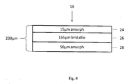
- a film 16 of three layers 24, 26, 28 can be made as shown in FIG. 4 is shown. Two different materials, amorphous and crystalline, are processed, whereby due to the different layer thicknesses, the film 16 becomes asymmetrical, since two outer layers 24 and 28 made of amorphous material have different thicknesses. The two outer layers 24 and 28 surround an inner layer 26 of crystalline material.
- the most advantageous variant is the film 16 with five layers as shown in FIG. 3 is described.
- This variant is also used in a plant with three extruders. In this case, three different formulations of material for each layer 18, 20 and 22 are used, and thus a symmetrical structure of the film 16 is achieved.
- renewable raw materials e.g. Polyhydroxyvalerates, abbreviated to PHV, polyhydroxybutyrates, abbreviated PHB, succinates, cellulose derivatives, etc., possible to produce a film with these according to their amorphous / crystalline structure.
- the film 16 is integrated over the entire area of the portable data carrier and is therefore part of the structure of the data carrier.
- additives can be integrated.
- a release additive a laser additive and / or a modifier are preferably integrated.
- a laser additive and / or a modifier are preferably integrated in the inner layers 20 and 22, a laser additive and / or a modifier are preferably integrated.
Landscapes
- Engineering & Computer Science (AREA)
- Ceramic Engineering (AREA)
- Computer Hardware Design (AREA)
- Microelectronics & Electronic Packaging (AREA)
- Physics & Mathematics (AREA)
- General Physics & Mathematics (AREA)
- Theoretical Computer Science (AREA)
- Laminated Bodies (AREA)
Abstract
Description
- Die vorliegende Erfindung beschreibt einen tragbaren Datenträger, der aus mehreren Folien aufgebaut ist, wobei die Folien aus nachwachsenden, zumindest teilweise kristallinen Rohstoffen bestehen. Im Datenträger ist ferner ein Chipmodul angeordnet.
- Aus dem Stand der Technik ist bekannt, dass tragbare Datenträger, z.B. Chipkarten, Kreditkarten, Bankkarten, Sozialversicherungskarten, SIM-Karten, etc., aus nachwachsenden Rohstoffen hergestellt werden. Insbesondere werden Karten aus nachwachsenden, teilkristallinen Rohstoffen, z.B. Poly-Lactid-Acid, abgekürzt PLA, hergestellt. Die Verwendung von teilkristallinen Materialien ist notwendig, um eine für tragbare Datenträger geforderte Temperaturstabilität zu erfüllen. Der Nachteil von teilkristallinen Materialien, wie z.B. Polymeren, ist, dass sie sich schlecht laminieren bzw. verkleben lassen. Um diesen Nachteil zu beheben, werden Folien aus teilkristallinen Materialien entweder mit einem Siebdruck-Lack, abgekürzt SD-Lack, als Laminierhilfe bedruckt oder es werden kleberbeschichtete Folien verwendet, um eine dauerhafte Verbindung bei einer Laminierung oder einer Klebeverbindung herzustellen. Eine weitere Möglichkeit zur Herstellung einer dauerhaften Verbindung bei Folien aus teilkristallinen Materialien ist die Verwendung von coextrudierten Folien, wobei auf den Außenseiten jeweils ein amorphes PLA angeordnet ist, was sehr dünn ist. Dies wird beispielsweise in der
DE-102013017927-A1 beschrieben. - Bei tragbaren Datenträgern aus nachwachsenden, teilkristallinen Materialien mit einem implantierten Chipmodul, das kontaktgebundene und/oder kontaktlose Schnittstellen aufweist, kommt es beim Implantieren der Chipmodule zu einer schlechten Verbindung zwischen Chipmodul und tragbaren Datenträger, d.h. die tragbaren Datenträger erfüllen nicht die gängigen Normen und bilden folglich ein sehr großes Risiko, dass tragbaren Datenträger im Feld ausfallen.
- Es ist deshalb Aufgabe der vorliegenden Erfindung eine Lösung für die oben beschriebenen Probleme zur Verfügung zu stellen.
- Die Aufgabe wird durch einen erfindungsgemäßen tragbaren Datenträger gelöst, der aus mehreren Folien aufgebaut ist, wobei die Folien aus nachwachsenden, zumindest teilweise kristallinen Rohstoffen bestehen, wobei ein Chipmodul im Datenträger angeordnet ist. Um die erfindungsgemäße Aufgabe zu lösen, umfasst der Datenträger mindestens eine Folie aus amorphen Material, wobei die Folie aus amorphen Material ohne Verwendung von Hilfsstoffen, wie sie bisher im Stand der Technik notwendig sind, eine dauerhafte Verbindung mit den angrenzenden Folien aus nachwachsenden Rohstoffen ausbildet. Ferner bildet die Folie aus amorphen Material eine dauerhafte Verbindung mittels eines Klebstoffs mit dem Chipmodul aus. Das Chipmodul wird mittels eines Klebstoffs mit dem tragbaren Datenträger dauerhaft verbunden. Der Klebstoff haftet nur an einem amorphen Material, z.B. einer amorphen Schicht einer entsprechenden Folie.
- Ein vorteilhaftes Ausführungsbeispiel der Erfindung ist, dass eine Schicht aus amorphen Material so in der Folie aus amorphen Material angeordnet ist, dass sie sich mit einer Verbindungsfläche des Chipmoduls in einer gemeinsamen Ebene befindet, um sich dauerhaft zu verbinden. Dies hat den Vorteil, dass die Schicht aus amorphen Material in einer gemeinsamen Ebene wie die Verbindungsfläche des Chipmoduls angeordnet ist, um eine möglichst große Verbindungsfläche zu erzeugen und folglich eine entsprechende feste und dauerhafte Verbindung zwischen Chipmodul und tragbaren Datenträger zu erzielen.
- Ein vorteilhaftes Ausführungsbeispiel der Erfindung ist, dass die Folie aus amorphen Material aus mindestens einer Schicht aus amorphen Material und mindestens einer Schicht aus kristallinen Material besteht. Durch den schichtweisen Aufbau aus amorphen und kristallinen Material können vorteilhaft z.B. die biegeelastischen Eigenschaften der Folie je nach Anwendung eingestellt werden.
- Ein weiteres vorteilhaftes Ausführungsbeispiel der Erfindung ist, dass die Folie aus amorphen Material auf mindestens einer Außenseite die Schicht aus amorphen Material aufweist. Der Vorteil der amorphen Schicht auf der Außenseite ist, dass eine dauerhafte Verbindung mit den benachbarten kristallinen Folien aus nachwachsenden Rohstoffen gebildet wird. Ferner kann über die Außenseite eine Verbindung mit dem Chipmodul hergestellt werden.
- Ein weiteres vorteilhaftes Ausführungsbeispiel der Erfindung ist, dass die Folie aus amorphen Material abwechselnd aus einer Schicht mit amorphen Material und aus einer Schicht mit kristallinen Material aufgebaut ist.
- Ein weiteres vorteilhaftes Ausführungsbeispiel der Erfindung ist, dass die Folie aus amorphen Material insgesamt aus drei oder fünf Schichten besteht. Eine technisch bevorzugte Ausführung ist eine Folie aus drei oder fünf Schichten aus sich abwechselnden amorphen und kristallinen Materialien, da gerade bei einer symmetrischen Struktur der Folie die vorteilhaftesten Eigenschaften bezüglich Ausbildung einer dauerhaften Verbindung mit benachbarten Folienschichten, als auch einer Verbindung mit dem Chipmodul erreicht werden. Je nach Lage der Verbindungsfläche des Chipmoduls kann die Lage einer entsprechenden amorphen Materialschicht in der Folie aus amorphen Material bestimmt werden, um eine möglichst dauerhafte Verbindung zu erhalten.
- Ein weiteres vorteilhaftes Ausführungsbeispiel der Erfindung ist, dass die Folie aus amorphen Material in mindestens einer Schicht mindestens einen Zusatzstoff enthält. Mittels Zusatzstoffen können die Eigenschaften der Folie z.B. hinsichtlich mechanischer Eigenschaften, Verarbeitbarkeit oder Markierbarkeit bestimmt werden. Als Zusatzstoffe bieten sich hierzu beispielsweise ein Laseradditiv, ein Releaseadditiv, und/oder ein Modifier an. Das Laseradditiv ermöglicht eine Personalisierung mittels Laser. Das Releaseadditiv trägt dazu bei, dass die Folie nicht an Rollen, z.B. Kalanderrollen, oder Laminierblechen haften bleibt. Der Modifier bezieht sich auf die Familie der sogenannten Impactmodifier, um z.B. einen Schlagzähmodifizierer der Folie einzustellen.
- Weitere Merkmale und Vorteile der Erfindung ergeben sich aus der folgenden Beschreibung von erfindungsgemäßen Ausführungsbeispielen sowie weiteren Ausführungsalternativen in Zusammenhang mit den Zeichnungen.
-
Figuren 1 und2 zeigen zwei unterschiedliche Aufbauten eines tragbaren Datenträgers gemäß Stand der Technik. -
Figur 3 zeigt ein erstes erfindungsgemäßes Ausführungsbeispiel einer symmetrischen Folie aus amorphen Material, die aus fünf Schichten besteht. -
Figur 4 zeigt ein zweites erfindungsgemäßes Ausführungsbeispiel einer unsymmetrischen Folie aus amorphen Material, die aus drei Schichten besteht. -
Figur 1 stellt beispielhaft einen tragbaren Datenträger 2 gemäß Stand der Technik dar, welcher aus zwei opaken Kernfolien 4 und zwei transparenten Overlayfolien 6 aufgebaut ist und typisch ist für Anwendungen mit einem kontaktbehafteten Chipmodul 8. Die Kernfolien 4 und die Overlayfolien 6 bestehen aus nachwachsenden Rohstoffen, z.B. PLA. -
Figur 2 stellt beispielhaft einen tragbaren Datenträger 10 gemäß Stand der Technik dar, welcher aus drei opaken Kernfolien 4 und zwei transparenten Overlayfolien 6 aufgebaut ist und typisch ist für Anwendungen mit einem kontaktbehafteten und kontaktlosen Chipmodul 12, sogenanntes Dualinterface-Modul. Wie oben bestehen auch hier die Kernfolien 4 und die Overlayfolien 6 aus nachwachsenden Rohstoffen, z.B. PLA. - Die
Figuren 1 und2 zeigen, dass die Kernfolien 4 in der Regel eine Dicke von 310µm bzw. 230µm und die Overlayfolien eine Dicke von 105µm haben. Um die Kernfolien 4 und die Overlayfolien 6 miteinander zu verbinden, ist zwischen den Kernfolien 4 und/oder zwischen den Kernfolien 4 und den Overlayfolien 6 ein Klebstoff oder ein Lack angeordnet oder es werden coextrudierte Folien mit einer dünnen amorphen Außenschicht verwendet werden, um eine Verbindung zwischen den Folien herzustellen. Die Klebe- oder Verbindungsfläche 14 des Chipmoduls 8, 12 befindet sich in der Regel in einer Tiefe von 210µm-230µm gemessen von einer Oberfläche des tragbaren Datenträgers 2, 10, je nach Modul 8, 12. Dabei müssen Toleranzen von +/- 15µm berücksichtigt werden. D.h. das Modul 8, 12 wird in ein kristallines, schwer verklebbares Material eingebracht und fixiert. Selbst mit ausgewählten Klebstoffen und Prozessparametern, z.B. Laminiertemperaturen, welche den tragbaren Datenträger beschädigen, kann keine ausreichend gute und stabile Qualität von Verbindungen zwischen dem Modul 8, 12 und dem tragbaren Datenträger 2, 10 erzielt werden. - Um dieses Problem zu lösen, wird eine coextrudierte Folie verwendet, wobei zur Verbindung des Moduls 8, 12 mit dem Datenträger 2, 10 eine Schicht der Folie aus einem amorphen Material besteht. Die Schicht wird so in der Folie positioniert, dass sie in einer Ebene mit der Verbindungsfläche des Chipmoduls 8, 12 liegt. Dazu werden beispielsweise in
Figur 2 die Kernfolien 4 mit einer Dicke von jeweils 230 µm ersetzt durch eine erfindungsgemäße Folie, wie sie inFigur 3 dargestellt ist. -
Figur 3 zeigt eine erfindungsgemäße Folie 16 aus amorphen Material, welche z.B. aus fünf Schichten besteht. Die Folie 16 weist auf ihren Außenseiten jeweils eine Schicht 18 aus amorphen Material mit einer Dicke von 15 µm auf. In der Mitte der Folie 16 befindet sich eine Schicht 20 aus amorphen Material mit einer Dicke von 50 µm. Zwischen den Schichten 18 und 20 befinden sich zwei Schichten 22 aus kristallinen Material mit einer Dicke von 75 µm. - Hergestellt wird die Folie 16 mittels drei Extrudern. Die Materialzusammensetzung für die Schichten 18, 20 und 22 sind unterschiedlich. Neben der Folie 16 mit fünf Schichten, kann auch eine Folie mit drei Schichten hergestellt werden. Optimal ist immer eine symmetrische Struktur der Folie. Grundsätzlich möglich ist auch eine Folie, die aus zwei Schichten besteht. Allerdings sind Folien aus zwei Schichten schwer herzustellen, aufgrund z.B. einer Wölbung der Folie oder von Spannungen im Material, und können meist nicht im optimalen Arbeitsbereich einer Extruderanlage hergestellt werden.
- Zur Herstellung der Folie 16 werden die Extruder in Form und Größe, d.h. Materialdurchsatz pro Stunde, der herzustellenden Folie angepasst. Wenn z.B. eine Folie mit einer dicken Innenschicht 20 aus einem Material C und einer dünnen Zwischenschicht 22 aus einem Material B und einer sehr dünnen Außenschicht 18 aus einem Material A hergestellt werden soll, dann werden die einzelnen Extruder z.B. folgendermaßen konfiguriert:
- Extruder für Material C: 275 kg/h Materialdurchsatz pro Stunde,
- Extruder für Material B: 150 kg/h Materialdurchsatz pro Stunde,
- Extruder für Material A: 75 kg/h Materialdurchsatz pro Stunde.
- Nur wenn die Extruder mit diesen Durchsätzen betrieben werden, dann erzielt man das beste Ergebnis, sowohl technisch als auch wirtschaftlich. Natürlich können die Durchsätze um ca. 25% verändert werden. Dies ist aber materialabhängig und verschlechtert in der Regel den Ertrag und die Qualität.
- Mit diesen drei Extrudern können z.B. folgende Konfigurationen von Folien hergestellt werden.
- Es kann eine Folie aus zwei Schichten hergestellt werden, wobei von zwei Extrudern das gleiche Material verarbeitet wird. Aufgrund der beiden Schichten entsteht ein unsymmetrischer Folienaufbau bestehend aus einer amorphen und einer kristallinen Schicht.
- Es kann eine Folie 16 aus drei Schichten 24, 26, 28 hergestellt werden, wie sie in
Figur 4 dargestellt ist. Es werden zwei verschiedene Materialien, amorph und kristallin, verarbeitet, wobei aufgrund der unterschiedlichen Schichtdicken die Folie 16 unsymmetrisch wird, da zwei Außenschichten 24 und 28 aus amorphen Material unterschiedlich dick sind. Die beiden Außenschichten 24 und 28 umgeben eine Innenschicht 26 aus kristallinen Material. - Die vorteilhafteste Variante ist die Folie 16 mit fünf Schichten, wie sie in
Figur 3 beschrieben wird. Diese Variante wird ebenfalls bei einer Anlage mit drei Extrudern verwendet. Dabei werden drei verschiedene Rezepturen von Material für jede Schicht 18, 20 und 22 verwendet und somit eine symmetrische Struktur der Folie 16 erreicht. - Die Schichten in
Figur 3 können beispielsweise aus folgenden Materialien bestehen: - Außenschicht 18: PLA, amorph, z.B. nature works 4060D,
- Zwischenschicht 22: PLA, kristallin, z.B. stereo complex PLA von Corbion,
- Innenschicht 20: PLA, amorph, z.B. nature works 4060D
- Grundsätzlich sind auch alle anderen geeigneten Materialien aus nachwachsenden Rohstoffen, z.B. Polyhydroxyvalerate, abgekürzt mit PHV, Polyhydroxybutyrate, abgekürzt PHB, Succinate, Cellulosederivate, etc., möglich, um mit diesen gemäß ihrer amorphen/kristallinen Struktur eine Folie herzustellen.
- Die Folie 16 wird über die gesamte Fläche des tragbaren Datenträgers integriert und ist folglich mit ein Bestandteil des Aufbaus des Datenträgers.
- In die einzelnen Schichten der Folie 16 können Zusatzstoffe integriert werden. In der Außenschicht 18 der Folie 16 werden vorzugsweise ein Releaseadditiv, ein Laseradditiv und/oder ein Modifier integriert. In den inneren Schichten 20 und 22 werden vorzugsweise ein Laseradditiv und /oder ein Modifier integriert.
-
- 2
- tragbarer Datenträger
- 4
- opake Kernfolien
- 6
- transparente Overlayfolie
- 8
- kontaktbehaftetes Chipmodul
- 10
- tragbarer Datenträger
- 12
- kontaktbehaftetes und kontaktloses Chipmodul, sog. Dualinterface
- 14
- Klebe- oder Verbindungsfläche des Chipmoduls
- 16
- erfindungsgemäße Folie aus amorphen Material
- 18
- Außenschicht aus amorphen Material
- 20
- Innenschicht aus amorphen Material
- 22
- Zwischenschicht aus kristallinen Material
- 24
- Außenschicht aus amorphen Material
- 26
- Innenschicht aus kristallinen Material
- 28
- Außenschicht aus amorphen Material
Claims (8)
- Tragbarer Datenträger (2, 10), der aus mehreren Folien (4, 6) aufgebaut ist, wobei die Folien (4, 6) aus nachwachsenden, zumindest teilweise kristallinen Rohstoffen bestehen,
wobei ein Chipmodul (8, 12) im Datenträger angeordnet ist,
dadurch gekennzeichnet, dass der Datenträger (2, 10) mindestens eine Folie (16) aus amorphen Material umfasst,
wobei die Folie (16) aus amorphen Material ohne Verwendung von Hilfsstoffen eine dauerhafte Verbindung sowohl mit den Folien (4, 6) aus nachwachsenden Rohstoffen als auch mit dem Chipmodul (8, 12) unter Verwendung eines Klebstoffs ausbildet. - Datenträger nach Anspruch 1, dadurch gekennzeichnet, dass eine Schicht (18, 20) aus amorphen Material so in der Folie (16) aus amorphen Material angeordnet ist, dass sie sich mit einer Verbindungsfläche (14) des Chipmoduls (8, 12) in einer gemeinsamen Ebene befindet, um sich dauerhaft zu verbinden.
- Datenträger nach Anspruch 2, dadurch gekennzeichnet, dass die Folie (16) aus amorphen Material aus mindestens einer Schicht (18, 20) aus amorphen Material und mindestens einer Schicht aus kristallinen Material (20) besteht.
- Datenträger nach Anspruch 3, dadurch gekennzeichnet, dass die Folie (16) aus amorphen Material auf mindestens einer Außenseite die Schicht (18) aus amorphen Material aufweist.
- Datenträger nach Anspruch 4, dadurch gekennzeichnet, dass die Folie (16) aus amorphen Material abwechselnd aus einer Schicht (18, 20) mit amorphen Material und aus einer Schicht (20) mit kristallinen Material aufgebaut ist.
- Datenträger nach Anspruch 5, dadurch gekennzeichnet, dass die Folie (16) aus amorphen Material insgesamt aus drei oder fünf Schichten besteht.
- Datenträger nach einem der vorhergehenden Ansprüche, dadurch gekennzeichnet, dass die Folie (16) aus amorphen Material in mindestens einer Schicht mindestens einen Zusatzstoff enthält.
- Datenträger nach Anspruch 7, dadurch gekennzeichnet, dass der Zusatzstoff ein Laseradditiv, ein Releaseadditiv, und/oder ein Modifier ist.
Applications Claiming Priority (1)
| Application Number | Priority Date | Filing Date | Title |
|---|---|---|---|
| DE102016000779.6A DE102016000779A1 (de) | 2016-01-26 | 2016-01-26 | Tragbarer Datenträger aus nachwachsenden Rohstoffen mit Chipmodul |
Publications (1)
| Publication Number | Publication Date |
|---|---|
| EP3199338A1 true EP3199338A1 (de) | 2017-08-02 |
Family
ID=57960218
Family Applications (1)
| Application Number | Title | Priority Date | Filing Date |
|---|---|---|---|
| EP17000118.4A Ceased EP3199338A1 (de) | 2016-01-26 | 2017-01-24 | Tragbarer datenträger aus nachwachsenden rohstoffen mit chipmodul |
Country Status (2)
| Country | Link |
|---|---|
| EP (1) | EP3199338A1 (de) |
| DE (1) | DE102016000779A1 (de) |
Citations (1)
| Publication number | Priority date | Publication date | Assignee | Title |
|---|---|---|---|---|
| DE102013017927A1 (de) | 2013-10-28 | 2015-04-30 | Giesecke & Devrient Gmbh | Verfahren zur Herstellung einer Folie und eines tragbaren Datenträgers |
-
2016
- 2016-01-26 DE DE102016000779.6A patent/DE102016000779A1/de active Pending
-
2017
- 2017-01-24 EP EP17000118.4A patent/EP3199338A1/de not_active Ceased
Patent Citations (1)
| Publication number | Priority date | Publication date | Assignee | Title |
|---|---|---|---|---|
| DE102013017927A1 (de) | 2013-10-28 | 2015-04-30 | Giesecke & Devrient Gmbh | Verfahren zur Herstellung einer Folie und eines tragbaren Datenträgers |
Also Published As
| Publication number | Publication date |
|---|---|
| DE102016000779A1 (de) | 2017-07-27 |
Similar Documents
| Publication | Publication Date | Title |
|---|---|---|
| EP2344342B1 (de) | Karte mit eingebettetem sicherheitselement | |
| DE102009058803A1 (de) | Datenträgerkarte und Verfahren zur Herstellung einer Datenträgerkarte | |
| EP2566702B1 (de) | Datenträger mit polymersubstrat mit motivbereich | |
| EP2936397B1 (de) | Verfahren zur herstellung eines inlays sowie inlay für einen folienverbund für ein wert- oder sicherheitsdokument | |
| EP2865517B1 (de) | Verfahren zur Herstellung einer Folie und eines tragbaren Datenträgers | |
| EP2095944A1 (de) | Chipkarten und Verfahren zum Herstellen einer Chipkarte | |
| EP3509806B1 (de) | Verfahren zur bearbeitung eines substrats mit einem stanzstempel | |
| EP1977891B1 (de) | Verfahren zur Herstellung von Kavitäten in Sicherheitsdokumenten, insbesondere Chipkarten | |
| WO2020064297A1 (de) | Verbundglasscheibe und verfahren zu deren herstellung | |
| DE112021004646T5 (de) | Gekrümmte lichtlenkungsstrukturen | |
| EP2906431A1 (de) | Buchartiges wert- und/oder sicherheitsdokument mit elastomerem buchrücken | |
| EP3092131B1 (de) | Verfahren zur herstellung eines sicherheitsdokuments | |
| DE102016000779A1 (de) | Tragbarer Datenträger aus nachwachsenden Rohstoffen mit Chipmodul | |
| DE102008022016A1 (de) | RFID-Inlays für elektronische Identifikationsdokumente und Herstellungsverfahren hierfür | |
| EP3489028A2 (de) | Verfahren zur herstellung eines buchartigen wert- und/oder sicherheitsdokuments sowie buchartiges wert- und/oder sicherheitsdokument | |
| DE102010023218A1 (de) | Verfahren zur Herstellung eines Wert- oder Sicherheitsdokuments mit einem Wasserzeichen | |
| WO2023051951A1 (de) | Schichtverbund für einen kartenförmigen datenträger, kartenförmiger datenträger und verfahren | |
| DE102020007084A1 (de) | Verfahren zum Herstellen eines mehrschichtigen Kartenkörpers | |
| DE102010055705A1 (de) | Heißlaminierbarer Schichtkörper mit mindestens einem elektrischen Schaltelement | |
| EP3418067A1 (de) | Fluoreszierende personalisierung mittels laser | |
| EP2669853A1 (de) | Tragbarer Datenträger | |
| DE102015008126A1 (de) | Kartenförmiger Datenträger mit farbiger Kante | |
| WO2002084585A1 (de) | Trägerfolie für elektronische bauelemente zur einlaminierung in chipkarten | |
| DE102009030818A1 (de) | Verfahren und Vorrichtung zum Herstellen eines Halbzeugs oder eines das Halbzeug umfassenden Sicherheitsdokuments | |
| WO2021028168A1 (de) | Wert- oder sicherheitsdokument und verfahren zu dessen herstellung |
Legal Events
| Date | Code | Title | Description |
|---|---|---|---|
| PUAI | Public reference made under article 153(3) epc to a published international application that has entered the european phase |
Free format text: ORIGINAL CODE: 0009012 |
|
| AK | Designated contracting states |
Kind code of ref document: A1 Designated state(s): AL AT BE BG CH CY CZ DE DK EE ES FI FR GB GR HR HU IE IS IT LI LT LU LV MC MK MT NL NO PL PT RO RS SE SI SK SM TR |
|
| AX | Request for extension of the european patent |
Extension state: BA ME |
|
| RAP1 | Party data changed (applicant data changed or rights of an application transferred) |
Owner name: GIESECKE+DEVRIENT MOBILE SECURITY GMBH |
|
| 17P | Request for examination filed |
Effective date: 20180202 |
|
| RBV | Designated contracting states (corrected) |
Designated state(s): AL AT BE BG CH CY CZ DE DK EE ES FI FR GB GR HR HU IE IS IT LI LT LU LV MC MK MT NL NO PL PT RO RS SE SI SK SM TR |
|
| 17Q | First examination report despatched |
Effective date: 20190709 |
|
| STAA | Information on the status of an ep patent application or granted ep patent |
Free format text: STATUS: THE APPLICATION HAS BEEN REFUSED |
|
| 18R | Application refused |
Effective date: 20191201 |