EP3196945B2 - Solar cell - Google Patents
Solar cell Download PDFInfo
- Publication number
- EP3196945B2 EP3196945B2 EP17152171.9A EP17152171A EP3196945B2 EP 3196945 B2 EP3196945 B2 EP 3196945B2 EP 17152171 A EP17152171 A EP 17152171A EP 3196945 B2 EP3196945 B2 EP 3196945B2
- Authority
- EP
- European Patent Office
- Prior art keywords
- semiconductor substrate
- transparent conductive
- layer
- conductive layer
- doped layer
- Prior art date
- Legal status (The legal status is an assumption and is not a legal conclusion. Google has not performed a legal analysis and makes no representation as to the accuracy of the status listed.)
- Active
Links
Images


Classifications
-
- B—PERFORMING OPERATIONS; TRANSPORTING
- B29—WORKING OF PLASTICS; WORKING OF SUBSTANCES IN A PLASTIC STATE IN GENERAL
- B29C—SHAPING OR JOINING OF PLASTICS; SHAPING OF MATERIAL IN A PLASTIC STATE, NOT OTHERWISE PROVIDED FOR; AFTER-TREATMENT OF THE SHAPED PRODUCTS, e.g. REPAIRING
- B29C64/00—Additive manufacturing, i.e. manufacturing of three-dimensional [3D] objects by additive deposition, additive agglomeration or additive layering, e.g. by 3D printing, stereolithography or selective laser sintering
- B29C64/20—Apparatus for additive manufacturing; Details thereof or accessories therefor
- B29C64/205—Means for applying layers
- B29C64/209—Heads; Nozzles
-
- B—PERFORMING OPERATIONS; TRANSPORTING
- B29—WORKING OF PLASTICS; WORKING OF SUBSTANCES IN A PLASTIC STATE IN GENERAL
- B29C—SHAPING OR JOINING OF PLASTICS; SHAPING OF MATERIAL IN A PLASTIC STATE, NOT OTHERWISE PROVIDED FOR; AFTER-TREATMENT OF THE SHAPED PRODUCTS, e.g. REPAIRING
- B29C64/00—Additive manufacturing, i.e. manufacturing of three-dimensional [3D] objects by additive deposition, additive agglomeration or additive layering, e.g. by 3D printing, stereolithography or selective laser sintering
- B29C64/10—Processes of additive manufacturing
- B29C64/106—Processes of additive manufacturing using only liquids or viscous materials, e.g. depositing a continuous bead of viscous material
-
- B—PERFORMING OPERATIONS; TRANSPORTING
- B33—ADDITIVE MANUFACTURING TECHNOLOGY
- B33Y—ADDITIVE MANUFACTURING, i.e. MANUFACTURING OF THREE-DIMENSIONAL [3-D] OBJECTS BY ADDITIVE DEPOSITION, ADDITIVE AGGLOMERATION OR ADDITIVE LAYERING, e.g. BY 3-D PRINTING, STEREOLITHOGRAPHY OR SELECTIVE LASER SINTERING
- B33Y40/00—Auxiliary operations or equipment, e.g. for material handling
-
- H—ELECTRICITY
- H02—GENERATION; CONVERSION OR DISTRIBUTION OF ELECTRIC POWER
- H02S—GENERATION OF ELECTRIC POWER BY CONVERSION OF INFRARED RADIATION, VISIBLE LIGHT OR ULTRAVIOLET LIGHT, e.g. USING PHOTOVOLTAIC [PV] MODULES
- H02S20/00—Supporting structures for PV modules
-
- H—ELECTRICITY
- H02—GENERATION; CONVERSION OR DISTRIBUTION OF ELECTRIC POWER
- H02S—GENERATION OF ELECTRIC POWER BY CONVERSION OF INFRARED RADIATION, VISIBLE LIGHT OR ULTRAVIOLET LIGHT, e.g. USING PHOTOVOLTAIC [PV] MODULES
- H02S30/00—Structural details of PV modules other than those related to light conversion
- H02S30/20—Collapsible or foldable PV modules
-
- H—ELECTRICITY
- H10—SEMICONDUCTOR DEVICES; ELECTRIC SOLID-STATE DEVICES NOT OTHERWISE PROVIDED FOR
- H10F—INORGANIC SEMICONDUCTOR DEVICES SENSITIVE TO INFRARED RADIATION, LIGHT, ELECTROMAGNETIC RADIATION OF SHORTER WAVELENGTH OR CORPUSCULAR RADIATION
- H10F10/00—Individual photovoltaic cells, e.g. solar cells
- H10F10/10—Individual photovoltaic cells, e.g. solar cells having potential barriers
- H10F10/16—Photovoltaic cells having only PN heterojunction potential barriers
- H10F10/164—Photovoltaic cells having only PN heterojunction potential barriers comprising heterojunctions with Group IV materials, e.g. ITO/Si or GaAs/SiGe photovoltaic cells
- H10F10/165—Photovoltaic cells having only PN heterojunction potential barriers comprising heterojunctions with Group IV materials, e.g. ITO/Si or GaAs/SiGe photovoltaic cells the heterojunctions being Group IV-IV heterojunctions, e.g. Si/Ge, SiGe/Si or Si/SiC photovoltaic cells
- H10F10/166—Photovoltaic cells having only PN heterojunction potential barriers comprising heterojunctions with Group IV materials, e.g. ITO/Si or GaAs/SiGe photovoltaic cells the heterojunctions being Group IV-IV heterojunctions, e.g. Si/Ge, SiGe/Si or Si/SiC photovoltaic cells the Group IV-IV heterojunctions being heterojunctions of crystalline and amorphous materials, e.g. silicon heterojunction [SHJ] photovoltaic cells
-
- H—ELECTRICITY
- H10—SEMICONDUCTOR DEVICES; ELECTRIC SOLID-STATE DEVICES NOT OTHERWISE PROVIDED FOR
- H10F—INORGANIC SEMICONDUCTOR DEVICES SENSITIVE TO INFRARED RADIATION, LIGHT, ELECTROMAGNETIC RADIATION OF SHORTER WAVELENGTH OR CORPUSCULAR RADIATION
- H10F19/00—Integrated devices, or assemblies of multiple devices, comprising at least one photovoltaic cell covered by group H10F10/00, e.g. photovoltaic modules
- H10F19/80—Encapsulations or containers for integrated devices, or assemblies of multiple devices, having photovoltaic cells
-
- H—ELECTRICITY
- H10—SEMICONDUCTOR DEVICES; ELECTRIC SOLID-STATE DEVICES NOT OTHERWISE PROVIDED FOR
- H10F—INORGANIC SEMICONDUCTOR DEVICES SENSITIVE TO INFRARED RADIATION, LIGHT, ELECTROMAGNETIC RADIATION OF SHORTER WAVELENGTH OR CORPUSCULAR RADIATION
- H10F71/00—Manufacture or treatment of devices covered by this subclass
-
- H—ELECTRICITY
- H10—SEMICONDUCTOR DEVICES; ELECTRIC SOLID-STATE DEVICES NOT OTHERWISE PROVIDED FOR
- H10F—INORGANIC SEMICONDUCTOR DEVICES SENSITIVE TO INFRARED RADIATION, LIGHT, ELECTROMAGNETIC RADIATION OF SHORTER WAVELENGTH OR CORPUSCULAR RADIATION
- H10F77/00—Constructional details of devices covered by this subclass
- H10F77/20—Electrodes
- H10F77/206—Electrodes for devices having potential barriers
- H10F77/211—Electrodes for devices having potential barriers for photovoltaic cells
- H10F77/215—Geometries of grid contacts
-
- H—ELECTRICITY
- H10—SEMICONDUCTOR DEVICES; ELECTRIC SOLID-STATE DEVICES NOT OTHERWISE PROVIDED FOR
- H10F—INORGANIC SEMICONDUCTOR DEVICES SENSITIVE TO INFRARED RADIATION, LIGHT, ELECTROMAGNETIC RADIATION OF SHORTER WAVELENGTH OR CORPUSCULAR RADIATION
- H10F77/00—Constructional details of devices covered by this subclass
- H10F77/20—Electrodes
- H10F77/206—Electrodes for devices having potential barriers
- H10F77/211—Electrodes for devices having potential barriers for photovoltaic cells
- H10F77/219—Arrangements for electrodes of back-contact photovoltaic cells
-
- H—ELECTRICITY
- H10—SEMICONDUCTOR DEVICES; ELECTRIC SOLID-STATE DEVICES NOT OTHERWISE PROVIDED FOR
- H10F—INORGANIC SEMICONDUCTOR DEVICES SENSITIVE TO INFRARED RADIATION, LIGHT, ELECTROMAGNETIC RADIATION OF SHORTER WAVELENGTH OR CORPUSCULAR RADIATION
- H10F77/00—Constructional details of devices covered by this subclass
- H10F77/20—Electrodes
- H10F77/244—Electrodes made of transparent conductive layers, e.g. transparent conductive oxide [TCO] layers
-
- H—ELECTRICITY
- H10—SEMICONDUCTOR DEVICES; ELECTRIC SOLID-STATE DEVICES NOT OTHERWISE PROVIDED FOR
- H10F—INORGANIC SEMICONDUCTOR DEVICES SENSITIVE TO INFRARED RADIATION, LIGHT, ELECTROMAGNETIC RADIATION OF SHORTER WAVELENGTH OR CORPUSCULAR RADIATION
- H10F77/00—Constructional details of devices covered by this subclass
- H10F77/30—Coatings
- H10F77/306—Coatings for devices having potential barriers
- H10F77/311—Coatings for devices having potential barriers for photovoltaic cells
- H10F77/315—Coatings for devices having potential barriers for photovoltaic cells the coatings being antireflective or having enhancing optical properties
-
- H—ELECTRICITY
- H10—SEMICONDUCTOR DEVICES; ELECTRIC SOLID-STATE DEVICES NOT OTHERWISE PROVIDED FOR
- H10F—INORGANIC SEMICONDUCTOR DEVICES SENSITIVE TO INFRARED RADIATION, LIGHT, ELECTROMAGNETIC RADIATION OF SHORTER WAVELENGTH OR CORPUSCULAR RADIATION
- H10F77/00—Constructional details of devices covered by this subclass
- H10F77/93—Interconnections
- H10F77/933—Interconnections for devices having potential barriers
- H10F77/935—Interconnections for devices having potential barriers for photovoltaic devices or modules
-
- Y—GENERAL TAGGING OF NEW TECHNOLOGICAL DEVELOPMENTS; GENERAL TAGGING OF CROSS-SECTIONAL TECHNOLOGIES SPANNING OVER SEVERAL SECTIONS OF THE IPC; TECHNICAL SUBJECTS COVERED BY FORMER USPC CROSS-REFERENCE ART COLLECTIONS [XRACs] AND DIGESTS
- Y02—TECHNOLOGIES OR APPLICATIONS FOR MITIGATION OR ADAPTATION AGAINST CLIMATE CHANGE
- Y02E—REDUCTION OF GREENHOUSE GAS [GHG] EMISSIONS, RELATED TO ENERGY GENERATION, TRANSMISSION OR DISTRIBUTION
- Y02E10/00—Energy generation through renewable energy sources
- Y02E10/50—Photovoltaic [PV] energy
Definitions
- Embodiments of the invention relate to a solar cell, and more particularly to a hetero-junction solar cell.
- hetero-junction solar cells include solar cells using intrinsic-amorphous silicon (i-a-Si) as a passivation layer, and solar cells using a thin tunnel oxide layer as a passivation layer.
- i-a-Si intrinsic-amorphous silicon
- the hetero-junction solar cells are formed on front and back surfaces of a semiconductor substrate for a solar cell and include a transparent conductive oxide (TCO) layer that performs an optical function (for example, a function of an anti-reflection layer and a reflection layer) and an electrical function (for example, a contact function with a metal electrode).
- TCO transparent conductive oxide
- EP 2 682 990 A1 discloses a heterojunction solar cell with a front layer and a back layer provided on the front and back surfaces of a semiconductor substrate, respectively, and overlapping each other on the side surface of the semiconductor substrate.
- the heterojunction solar cell also comprises an electrically conductive back coating which is formed with a distance to the edge of the semiconductor substrate and a front anti-reflection coating which covers the whole surface of the front layer and may also extend to the side surface of the semiconductor substrate.
- KR 2012 0104846 A discloses a solar battery and a manufacturing method thereof in which a first conductive layer is formed on a first semiconductor layer, a first electrode is formed on the first conductive layer, a second semiconductor layer is formed on the other side of the semiconductor wafer, the second semiconductor layer has different polarity with the first semiconductor layer, a second conductive layer is formed on the second semiconductor layer, a second electrode is formed on the second conductive layer, and the first conductive layer and the second conductive layer are formed in order not to contact each other in a side of the semiconductor wafer.
- EP 1 696 492 A1 discloses a photovoltaic cell in which a first electrode layer is formed so as to cover a region extending to an outer periphery of a semiconductor.
- An object of the invention is to provide a high-efficiency solar cell.
- a width in a first direction of the front transparent conductive layer may be equal to or greater than a width in the first direction of the semiconductor substrate.
- a region where the front transparent conductive layer is not formed is locally located in a part of the edge region of the front surface of the semiconductor substrate.
- a plurality of regions where the front transparent conductive layer is not formed may be spaced apart from each other.
- a width in the first direction and a width in a second direction of the back transparent conductive layer may be less than the width in the first direction and a width in the second direction of the semiconductor substrate, respectively.
- the back transparent conductive layer may be not formed in an edge region of the back surface of the semiconductor substrate.
- a region where the back transparent conductive layer is not formed is continuously formed along an edge of the semiconductor substrate.
- each of the front surface and the back surface of the semiconductor substrate Includes an edge region that is continuously formed from an edge of the semiconductor substrate to inside of the semiconductor substrate along the edge and a center region that is a remaining region except for the edge region.
- the front transparent conductive layer is formed in the center region and a remaining edge region except for a non-formed portion formed discontinuously in a part of the edge region of the front surface.
- the back transparent conductive layer is formed only in the center region except for the edge region of the back surface.
- the physical connection or physical contact between the front transparent conductive layer and the back transparent conductive layer is completely prevented and the size of the front transparent conductive layer located on the front surface of the semiconductor substrate on which light is incident can be maximized.
- the back collector electrode includes a plurality of second finger electrodes extending in the first direction and at least one second bus bar electrode extending in the second direction and physically connected to the plurality of second finger electrodes, or include a sheet electrode which covers entirely the back surface of the back transparent conductive layer.
- the non-formed portion is located at both ends of the at least one first bus bar electrode.
- a width in the first direction of the both ends of the at least one first bus bar electrode is larger than a width in the first direction of a remaining portion located between the both ends along the second direction.
- Each of the both ends of the at least one first bus bar electrode is divided into both sides of the non-forming portion along the first direction, and the non-formed portion is located between the divided both ends.
- a width in the first direction of the non-formed portion may be less than the width in the first direction of the remaining portion of the at least one first bus bar electrode.
- a length in the second direction of the non-formed portion may be smaller than an interval between two first finger electrodes that is adjacent to each other in the second direction.
- a solar cell according to an embodiment of the invention further includes a front passivation layer located between the front doped layer and the semiconductor substrate, and a back passivation layer located between the back doped layer and the semiconductor substrate.
- the front passivation layer and the back passivation layer may be formed of intrinsic amorphous silicon or a tunnel oxide.
- the front passivation layer and the back passivation layer are further located on a side surface of the semiconductor substrate.
- the front passivation layer, the back passivation layer, the front doped layer, and the back doped layer may overlap each other on the side surface of the semiconductor substrate.
- a passivation effect on the side surface of the semiconductor substrate can be obtained.
- the front transparent conductive layer is located on the front passivation layer and the back passivation layer which overlap each other on the side surface of the semiconductor substrate.
- the physical connection or physical contact between the front transparent conductive layer and the back transparent conductive layer is completely prevented and the size of the front transparent conductive layer located on the front surface of the semiconductor substrate on which light is incident can be maximized. Therefore, it is possible to achieve a high efficiency of the solar cell.
- a first component may be designated as a second component without departing from the scope of the embodiments of the invention.
- the second component may be designated as the first component.
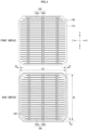
- FIG. 1 is a front view and a back view of a solar cell according to a first embodiment, which does not form part of the invention but is illustrated as a mere example suitable for understanding the invention.
- FIG. 2 is a cross-sectional view of a solar cell shown in FIG. 1 cut along line II-II in the X-X direction.
- FIG. 3 is a front view and a back view showing a state in which a front collector electrode and a back collector electrode are removed from a solar cell shown in FIG. 1 .
- a solar cell according to the first embodiment includes a crystalline semiconductor substrate 110.
- a front passivation layer 120, a front doped layer 130, a front transparent conductive layer 140, and a front collector electrode 150 are sequentially stacked on the front surface (or a light incident surface) of the semiconductor substrate 110.
- a back passivation layer 160, a back doped layer 170, a back transparent conductive layer 180, and a back collector electrode 190 are sequentially stacked on the back surface of the semiconductor substrate 110.
- front surface refers to an upward facing surface in the accompanying drawings.
- back surface refers to a downward facing surface in the accompanying drawings.
- side surface refers to a surface facing both left and right sides in the accompanying drawings.
- front surface refers to a surface on which a transparent conductive layer having a relatively wide width is located among the transparent conductive layers 140 and 180. The surface on which the transparent conductive layer having a relatively wide width is located can be used as the front surface or the light incidence surface.
- the substrate 110 is a semiconductor substrate 110 made of crystalline silicon containing impurities of a first conductive type, for example, an n-type.
- the silicon may be single crystal silicon or polycrystalline silicon.
- the substrate 110 contains impurities of a Group V element such as phosphorus (P), arsenic (As), antimony (Sb), and the like.
- a Group V element such as phosphorus (P), arsenic (As), antimony (Sb), and the like.
- the substrate 110 may be a p-type and may be made of a semiconductor material other than silicon.
- the substrate 110 may contain impurities of a Group III element such as boron (B), gallium (Ga), indium (In), and the like.
- the substrate 110 has an n-type.
- the substrate 110 has a texturing surface whose surface is textured. More specifically, the substrate 110 includes a front surface on which the front passivation layer 120 is located and a back surface on which the back passivation layer 160 is located as texturing surfaces.
- the back surface of the semiconductor substrate 110 may be formed as a substantially flat surface without fine unevenness.
- the front passivation layer 120 located on the front surface of the semiconductor substrate 110 and the back passivation layer 160 located on the back surface of the semiconductor substrate 110 may be formed of substantially intrinsic i-type amorphous silicon (i-a-Si) or may be formed of a tunnel oxide.
- the front passivation layer 120 extends to the side surface of the substrate 110 and the back passivation layer 160 extends to the side surface of the substrate 110.
- the front passivation layer 120 and the back passivation layer 160 overlap each other on the side surface of the semiconductor substrate 110. Therefore, since the passivation effect at the side surface of the semiconductor substrate can be obtained, the passivation effect can be improved as compared with the instance where the side surface of the semiconductor substrate is not covered with the front and back passivation layers.
- overlap each other refers to a state in which at least a part of the front passivation layer and the back passivation layer overlaps each other on a projection surface when viewed from the side surface of the semiconductor substrate.
- the front doped layer 130 located on the front passivation layer 120 is an impurity portion having a second conductive type, for example, a p-type opposite the conductive type of the substrate 110.
- the front doped layer 130 is made of p-type amorphous silicon (p-a-Si) and forms a p-n junction and a hetero junction with the substrate 110.
- the back doped layer 170 located under the back passivation layer 160, that is, on the back surface of the semiconductor substrate 110 is an impurity portion having a first conductive type, for example, an n-type, which is the same as the conductive type of the substrate 110.
- the back doped layer 170 is made of n-type amorphous silicon and forms a hetero junction with the substrate 110.
- the front doped layer 130 located on the front surface (or the light incident surface) of the semiconductor substrate may be made of n-type amorphous silicon (n-a-Si).
- the back doped layer 170 located on the back surface (or the surface opposite to the light incident surface) of the semiconductor substrate may be made of p-type amorphous silicon (p-a-Si).
- the separated electrons move toward the back doped layer 170 and the separated holes move toward the front doped layer 130.
- the separated holes move toward the back doped layer 170, and the separated electrons move toward the front doped layer 130.
- the front passivation layer 120, the front doped layer 130, the back passivation layer 160, and the back doped layer 170 are sequentially stacked on the side surface of the semiconductor substrate 110 and overlap each other.
- the front doped layer may be formed only on the front surface of the semiconductor substrate
- the back doped layer may be formed only on the back surface of the semiconductor substrate. In this instance, only the front passivation layer and the back passivation layer overlap each other on the side surface of the semiconductor substrate.
- the back collector electrode 190 is composed of the plurality of second finger electrodes 190a and the second bus bar electrode 190b.
- the solar cell having the back collector electrode 190' as a sheet electrode since light cannot be incident on the back surface of the semiconductor substrate 110, the solar cell having the back collector electrode 190' as a sheet electrode can be used as a mono-facial solar cell.
- the solar cell module can be manufactured by electrically connecting a plurality of solar cells using wirings (for example, interconnectors or ribbons), disposing the plurality of solar cells between a pair of substrates, and performing a lamination process in a state where a sealing material is disposed between the pair of substrates.
- wirings for example, interconnectors or ribbons
- n-type single crystal silicon substrate is cleaned to remove impurities, and etching is performed using an etchant composed of an aqueous solution of sodium hydroxide.
- a semiconductor substrate 110 having texturing surfaces formed on front and back surfaces of the silicon substrate is prepared.
- a front passivation layer 120 made of i-type amorphous silicon and a front doped layer 130 made of p-type amorphous silicon are sequentially formed on the front surface and the side surface of the substrate 110, and a back passivation layer 160 made of i-type amorphous silicon and a back doped layer 170 made of n-type amorphous silicon are sequentially formed on the back surface and the side surface of the substrate 110.
- RF radio-frequency
- CVD chemical vapor deposition
- the front passivation layer 120, the front doped layer 130, the back passivation layer 160, and the back doped layer 170 overlap each other on the side surface of the semiconductor substrate 110.
- a front transparent conductive layer 140 is formed on the front doped layer 130 and a back transparent conductive layer 180 is formed on the back surface of the back doped layer 170.
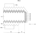
- the sputtering device shown in FIG. 7 is a device capable of simultaneously forming transparent conductive layers 140 and 180 on both surfaces of the semiconductor substrate 110, that is, a front surface and a back surface.
- Each of the sputtering targets 200 is located above the front surface and below the back surface of the semiconductor substrate 110 placed on a tray 210.
- the front transparent conductive layer 140 and the back transparent conductive layer 180 can be simultaneously formed in the same sputtering process.
- the tray 210 holding the semiconductor substrate 110 has a contact portion 212 that is physically and directly in contact with the back surface of the semiconductor substrate 110.
- the contact portion 212 is formed as a shape that covers the edge region A1 of the back surface of the semiconductor substrate 110.
- the front transparent conductive layer 140 and the back transparent conductive layer 180 are formed using the sputtering device shown in FIG. 7 , the front transparent conductive layer 140 is formed entirely in the center region A2 and the edge region A1 of the front surface of the semiconductor substrate 110 and extends to the side surface of the semiconductor substrate 110.
- the back transparent conductive layer 180 is formed only in the central region A2 of the back surface of the semiconductor substrate 110.
- the front passivation layer 120, the front doped layer 130, the back passivation layer 160, and the back doped layer 170 overlap each other on the side surface of the semiconductor substrate 110.
- the RPD device shown in FIG. 8 is a device capable of sequentially forming transparent conductive layers 140 and 180 on both surfaces of the semiconductor substrate 110, that is, a front surface and a back surface by flipping the semiconductor substrate 110.
- the sputtering target 200 is located only below the back surface of the semiconductor substrate 110 placed on a tray 210 and 220.
- the back transparent conductive layer 180 and the front transparent conductive layer 140 can be sequentially formed.
- the tray 210 holding the semiconductor substrate 110 to form the back transparent conductive layer 180 has a contact portion 212 that is physically and directly in contact with the back surface of the semiconductor substrate 110.
- the contact portion 212 is formed of a shape that covers the edge region A1 of the back surface of the semiconductor substrate 110.
- the tray 220 holding the semiconductor substrate 110 to form the front transparent conductive layer 140 has a contact portion 222 that is physically and directly in contact with the front surface of the semiconductor substrate 110.
- the contact portion 222 is formed as a shape that covers the non-formed portion A3 in the edge region A1 of the first surface of the semiconductor substrate 110.
- the back transparent conductive layer 180 when the back transparent conductive layer 180 are formed using the RPD device shown in FIG. 8 , the back transparent conductive layer 180 may be formed only in the center region A2 of the back surface of the semiconductor substrate 110.
- the front transparent conductive layer 140 when the front transparent conductive layer 140 is formed in a state in which the semiconductor substrate 110 is placed on the tray 220 so that the front surface of the semiconductor substrate 110 is in contact with the contact portion 222 of the tray 220 by flipping the semiconductor substrate 110, the front transparent conductive layer 140 may be formed in the center region A2 of the front surface of the semiconductor substrate 110 and in the edge region A1 except for the non-formed portion A3.
- an annealing process for crystallizing the front transparent conductive layer 140 and the back transparent conductive layer 180 may be performed, and the front collector electrode 150 and the back collector electrode 190 may be formed using a screen printing method.
Landscapes
- Engineering & Computer Science (AREA)
- Chemical & Material Sciences (AREA)
- Materials Engineering (AREA)
- Manufacturing & Machinery (AREA)
- Physics & Mathematics (AREA)
- Mechanical Engineering (AREA)
- Optics & Photonics (AREA)
- Photovoltaic Devices (AREA)
- Life Sciences & Earth Sciences (AREA)
- Sustainable Development (AREA)
- Sustainable Energy (AREA)
Description
- Embodiments of the invention relate to a solar cell, and more particularly to a hetero-junction solar cell.
- Recently, research on hetero-junction solar cells has been progressing in order to improve the efficiency of solar cells. Representative hetero-junction solar cells include solar cells using intrinsic-amorphous silicon (i-a-Si) as a passivation layer, and solar cells using a thin tunnel oxide layer as a passivation layer.
- The hetero-junction solar cells are formed on front and back surfaces of a semiconductor substrate for a solar cell and include a transparent conductive oxide (TCO) layer that performs an optical function (for example, a function of an anti-reflection layer and a reflection layer) and an electrical function (for example, a contact function with a metal electrode).
- When a front transparent conductive layer located on the front surface of the semiconductor substrate and a back transparent conductive layer located under the back surface of the semiconductor substrate physically come into contact with each other, there is a problem that the shunt resistance is lowered, the conversion efficiency is lowered, and a short circuit occurs.
- Accordingly, a related art solar cell was configured such that a transparent conductive layer was not formed in the front edge region and the back edge region of the semiconductor substrate but only in the center region except for the edge region.
EP 2 682 990 A1 discloses a heterojunction solar cell with a front layer and a back layer provided on the front and back surfaces of a semiconductor substrate, respectively, and overlapping each other on the side surface of the semiconductor substrate. The heterojunction solar cell also comprises an electrically conductive back coating which is formed with a distance to the edge of the semiconductor substrate and a front anti-reflection coating which covers the whole surface of the front layer and may also extend to the side surface of the semiconductor substrate.KR 2012 0104846 A EP 1 696 492 A1JP 2001 044461 A JP 2011 023758 A - However, in the solar cell having such a structure, since the front transparent conductive layer is not formed in the edge region, the anti-reflection function of the front transparent conductive layer is deteriorated, and currents generated in the semiconductor substrate of the edge region are not collected on the collector electrode. Therefore, there is a problem that the short-circuit current density is reduced and thus the efficiency of the solar cell is lowered.
- An object of the invention is to provide a high-efficiency solar cell.
- A solar cell according to the present invention is defined in
claim 1. Preferred features are defined in the dependent claims. - In one example useful for understanding the present invention, there is provided a solar cell including a crystalline semiconductor substrate of a first conductive type; a front doped layer located on a front surface of the semiconductor substrate and forming a hetero junction with the semiconductor substrate; a back doped layer located on a back surface of the semiconductor substrate and forming a hetero junction with the semiconductor substrate; a front transparent conductive layer located on the front doped layer; and a back transparent conductive layer located under the back doped layer. One of the front doped layer and the back doped layer has a second conductive type opposite the first conductive type to form a p-n junction with the semiconductor substrate, and the other of the front doped layer and the back doped layer has the first conductive type. A planar area of the front transparent conductive layer is larger than a planar area of the back transparent conductive layer.
- A width in a first direction of the front transparent conductive layer may be equal to or greater than a width in the first direction of the semiconductor substrate.
- The front transparent conductive layer is not formed in at least a part of an edge region of the front surface of the semiconductor substrate.
- A region where the front transparent conductive layer is not formed is locally located in a part of the edge region of the front surface of the semiconductor substrate.
- A plurality of regions where the front transparent conductive layer is not formed may be spaced apart from each other.
- A width in the first direction and a width in a second direction of the back transparent conductive layer may be less than the width in the first direction and a width in the second direction of the semiconductor substrate, respectively.
- The back transparent conductive layer may be not formed in an edge region of the back surface of the semiconductor substrate.
- A region where the back transparent conductive layer is not formed is continuously formed along an edge of the semiconductor substrate.
- In an embodiment of the invention, each of the front surface and the back surface of the semiconductor substrate Includes an edge region that is continuously formed from an edge of the semiconductor substrate to inside of the semiconductor substrate along the edge and a center region that is a remaining region except for the edge region. The front transparent conductive layer is formed in the center region and a remaining edge region except for a non-formed portion formed discontinuously in a part of the edge region of the front surface. The back transparent conductive layer is formed only in the center region except for the edge region of the back surface.
- According to the solar cell having such a configuration, the physical connection or physical contact between the front transparent conductive layer and the back transparent conductive layer is completely prevented and the size of the front transparent conductive layer located on the front surface of the semiconductor substrate on which light is incident can be maximized.
- Therefore, it is possible to achieve a high efficiency of the solar cell.
- A width of the edge region of the back surface of the semiconductor substrate may be 0.5 mm to 1.5 mm, for example, 0.5 mm to 1.0 mm.
- At least one of the front surface and the back surface of the semiconductor substrate may be formed as a texturing surface including a plurality of fine unevenness.
- The semiconductor substrate contains an n-type impurity, the front doped layer may be formed of p-type amorphous silicon containing a p-type impurity, and the back doped layer may be formed of n-type amorphous silicon containing an n-type impurity.
- A solar cell according to an embodiment of the invention further includes a front collector electrode located on the front transparent conductive layer and a back collector electrode located under the back transparent conductive layer. The front collector electrode is not physically and directly in contact with the front doped layer and the back collector electrode may be not physically and directly in contact with the back doped layer.
- According to this structure, defects can be prevented from being generated in the doped layer when the electrode (e.g., a metal material) is baked.
- The front collector electrode includes a plurality of first finger electrodes extending in the first direction, and at least one first bus bar electrode extending in the second direction orthogonal to the first direction and physically connected to the plurality of first finger electrodes.
- The back collector electrode includes a plurality of second finger electrodes extending in the first direction and at least one second bus bar electrode extending in the second direction and physically connected to the plurality of second finger electrodes, or include a sheet electrode which covers entirely the back surface of the back transparent conductive layer.
- According to an embodiment of the invention, the non-formed portion is located at both ends of the at least one first bus bar electrode.
- A width in the first direction of the both ends of the at least one first bus bar electrode is larger than a width in the first direction of a remaining portion located between the both ends along the second direction. Each of the both ends of the at least one first bus bar electrode is divided into both sides of the non-forming portion along the first direction, and the non-formed portion is located between the divided both ends.
- In this instance, the first finger electrodes may be located on the front transparent conductive layer of the edge region excluding the non-forming portion, and the both ends of the divided at least one first bus bar electrode may extend to the edge region and may be physically connected to the first finger electrodes.
- A width in the first direction of the non-formed portion may be less than the width in the first direction of the remaining portion of the at least one first bus bar electrode. A length in the second direction of the non-formed portion may be smaller than an interval between two first finger electrodes that is adjacent to each other in the second direction.
- A solar cell according to an embodiment of the invention further includes a front passivation layer located between the front doped layer and the semiconductor substrate, and a back passivation layer located between the back doped layer and the semiconductor substrate. The front passivation layer and the back passivation layer may be formed of intrinsic amorphous silicon or a tunnel oxide.
- The front passivation layer and the back passivation layer are further located on a side surface of the semiconductor substrate. The front passivation layer, the back passivation layer, the front doped layer, and the back doped layer may overlap each other on the side surface of the semiconductor substrate. As described above, when the front passivation layer, the back passivation layer, the front doped layer, and the back doped layer overlap each other on the side surface of the semiconductor substrate, a passivation effect on the side surface of the semiconductor substrate can be obtained. Of course, even if only the front passivation layer and the back passivation layer overlap each other on the side surface of the semiconductor substrate, and the front doped layer and the back doped layer are not located further on the side surface of the semiconductor substrate, a passivation effect can be obtained by the front passivation layer and the back passivation layer which overlap each other on the side surface of the semiconductor substrate.
- In this instance, the front transparent conductive layer is located on the front passivation layer and the back passivation layer which overlap each other on the side surface of the semiconductor substrate.
- In a solar cell according to an embodiment of the invention, the physical connection or physical contact between the front transparent conductive layer and the back transparent conductive layer is completely prevented and the size of the front transparent conductive layer located on the front surface of the semiconductor substrate on which light is incident can be maximized. Therefore, it is possible to achieve a high efficiency of the solar cell.
-
-
FIG. 1 is a front view and a back view of a solar cell according to a first embodiment. -
FIG. 2 is a cross-sectional view of a solar cell shown inFIG. 1 cut along line II-II. -
FIG. 3 is a front view and a back view showing a state in which a front collector electrode and a back collector electrode are removed from a solar cell shown inFIG. 1 . -
FIG. 4 is a front view of a solar cell according to a second embodiment of the invention. -
FIG. 5 is a front view showing a state in which a front collector electrode is removed from the solar cell shown inFIG. 4 . -
FIG. 6 is a cross-sectional view of a solar cell according to a third embodiment. -
FIG. 7 is a device for forming a transparent conductive layer of the solar cell shown inFIG. 1 , and a conceptual diagram of a sputtering device capable of simultaneous deposition on both surfaces. -
FIG. 8 illustrates a device for forming a transparent conductive layer of the solar cell shown inFIG. 4 , and a conceptual diagram of a remote plasma deposition (RPD) device capable of depositing both surfaces using flipping. - Reference will now be made in detail to embodiments of the invention examples of which are illustrated in the accompanying drawings. Since the invention may be modified in various ways and may have various forms, specific embodiments are illustrated in the drawings and are described in detail in the specification. However, it should be understood that the invention are not limited to specific disclosed embodiments, but include all modifications, equivalents and substitutes included within the technical scope of the invention.
- The terms 'first', 'second', etc., may be used to describe various components, but the components are not limited by such terms. The terms are used only for the purpose of distinguishing one component from other components.
- For example, a first component may be designated as a second component without departing from the scope of the embodiments of the invention. In the same manner, the second component may be designated as the first component.
- The term "and/or" encompasses both combinations of the plurality of related items disclosed and any item from among the plurality of related items disclosed.
- When an arbitrary component is described as "being connected to" or "being linked to" another component, this should be understood to mean that still another component(s) may exist between them, although the arbitrary component may be directly connected to, or linked to, the second component.
- On the other hand, when an arbitrary component is described as "being directly connected to" or "being directly linked to" another component, this should be understood to mean that no other component exists between them.
- The terms used in this application are used to describe only specific embodiments or examples, and are not intended to limit the invention. A singular expression can include a plural expression as long as it does not have an apparently different meaning in context.
- In this application, the terms "include" and "have" should be understood to be intended to designate that illustrated features, numbers, steps, operations, components, parts or combinations thereof exist and not to preclude the existence of one or more different features, numbers, steps, operations, components, parts or combinations thereof, or the possibility of the addition thereof.
- In the drawings, the thickness of layers, films, panels, regions, etc., are exaggerated for clarity. It will be understood that when an element such as a layer, film, region, or substrate is referred to as being "on" another element, it can be directly on the other element or intervening elements may also be present. In contrast, when an element is referred to as being "directly on" another element, there are no intervening elements present.
- Unless otherwise specified, all of the terms which are used herein, including the technical or scientific terms, have the same meanings as those that are generally understood by a person having ordinary knowledge in the art to which the invention pertains.
- The terms defined in a generally used dictionary must be understood to have meanings identical to those used in the context of a related art, and are not to be construed to have ideal or excessively formal meanings unless they are obviously specified in this application.
- The following example embodiments of the invention are provided to those skilled in the art in order to describe the invention more completely. Accordingly, shapes and sizes of elements shown in the drawings may be exaggerated for clarity.
- Example embodiments of the invention will be described with reference to the accompanying drawings.
-
FIG. 1 is a front view and a back view of a solar cell according to a first embodiment, which does not form part of the invention but is illustrated as a mere example suitable for understanding the invention.FIG. 2 is a cross-sectional view of a solar cell shown inFIG. 1 cut along line II-II in the X-X direction.FIG. 3 is a front view and a back view showing a state in which a front collector electrode and a back collector electrode are removed from a solar cell shown inFIG. 1 . - As shown in
FIGS. 1 to 3 , a solar cell according to the first embodiment includes acrystalline semiconductor substrate 110. - A
front passivation layer 120, a front dopedlayer 130, a front transparentconductive layer 140, and afront collector electrode 150 are sequentially stacked on the front surface (or a light incident surface) of thesemiconductor substrate 110. Aback passivation layer 160, a back dopedlayer 170, a back transparentconductive layer 180, and aback collector electrode 190 are sequentially stacked on the back surface of thesemiconductor substrate 110. - Hereinafter, the "front surface" refers to an upward facing surface in the accompanying drawings. The "back surface" refers to a downward facing surface in the accompanying drawings. The "side surface" refers to a surface facing both left and right sides in the accompanying drawings. The "front surface" refers to a surface on which a transparent conductive layer having a relatively wide width is located among the transparent
conductive layers - The
substrate 110 is asemiconductor substrate 110 made of crystalline silicon containing impurities of a first conductive type, for example, an n-type. In this instance, the silicon may be single crystal silicon or polycrystalline silicon. - Since the
substrate 110 has an n-type, thesubstrate 110 contains impurities of a Group V element such as phosphorus (P), arsenic (As), antimony (Sb), and the like. - Alternatively, however, the
substrate 110 may be a p-type and may be made of a semiconductor material other than silicon. When thesubstrate 110 has a p-type, thesubstrate 110 may contain impurities of a Group III element such as boron (B), gallium (Ga), indium (In), and the like. - Hereinafter, a case that the
substrate 110 has an n-type will be described as an example. - The
substrate 110 has a texturing surface whose surface is textured. More specifically, thesubstrate 110 includes a front surface on which thefront passivation layer 120 is located and a back surface on which theback passivation layer 160 is located as texturing surfaces. - Alternatively, the back surface of the
semiconductor substrate 110 may be formed as a substantially flat surface without fine unevenness. - The
front passivation layer 120 located on the front surface of thesemiconductor substrate 110 and theback passivation layer 160 located on the back surface of thesemiconductor substrate 110 may be formed of substantially intrinsic i-type amorphous silicon (i-a-Si) or may be formed of a tunnel oxide. - The
front passivation layer 120 extends to the side surface of thesubstrate 110 and theback passivation layer 160 extends to the side surface of thesubstrate 110. In this instance, thefront passivation layer 120 and theback passivation layer 160 overlap each other on the side surface of thesemiconductor substrate 110. Therefore, since the passivation effect at the side surface of the semiconductor substrate can be obtained, the passivation effect can be improved as compared with the instance where the side surface of the semiconductor substrate is not covered with the front and back passivation layers. In this instance, "overlap each other" refers to a state in which at least a part of the front passivation layer and the back passivation layer overlaps each other on a projection surface when viewed from the side surface of the semiconductor substrate. - The front doped
layer 130 located on thefront passivation layer 120 is an impurity portion having a second conductive type, for example, a p-type opposite the conductive type of thesubstrate 110. The front dopedlayer 130 is made of p-type amorphous silicon (p-a-Si) and forms a p-n junction and a hetero junction with thesubstrate 110. - The back doped
layer 170 located under theback passivation layer 160, that is, on the back surface of thesemiconductor substrate 110 is an impurity portion having a first conductive type, for example, an n-type, which is the same as the conductive type of thesubstrate 110. The back dopedlayer 170 is made of n-type amorphous silicon and forms a hetero junction with thesubstrate 110. - Alternatively, the front doped
layer 130 located on the front surface (or the light incident surface) of the semiconductor substrate may be made of n-type amorphous silicon (n-a-Si). The back dopedlayer 170 located on the back surface (or the surface opposite to the light incident surface) of the semiconductor substrate may be made of p-type amorphous silicon (p-a-Si). - When the
semiconductor substrate 110 and the back dopedlayer 170 are n-type and the front dopedlayer 130 is p-type, the separated electrons move toward the back dopedlayer 170 and the separated holes move toward the front dopedlayer 130. - Unlike the embodiment, when the
substrate 110 and the back dopedlayer 170 are p-type and the front dopedlayer 130 is n-type, the separated holes move toward the back dopedlayer 170, and the separated electrons move toward the front dopedlayer 130. - Each of the front doped
layer 130 and the back dopedlayer 170 may be formed to extend to the side surface of thesemiconductor substrate 110. - Therefore, the
front passivation layer 120, the front dopedlayer 130, theback passivation layer 160, and the back dopedlayer 170 are sequentially stacked on the side surface of thesemiconductor substrate 110 and overlap each other. However, the front doped layer may be formed only on the front surface of the semiconductor substrate, and the back doped layer may be formed only on the back surface of the semiconductor substrate. In this instance, only the front passivation layer and the back passivation layer overlap each other on the side surface of the semiconductor substrate. - Each of the front surface and the back surface of the
semiconductor substrate 110 includes an edge region A1 that is continuously formed along an edge from an edge of thesemiconductor substrate 110 to inside of thesemiconductor substrate 110 and a center region A2 that is a remaining region except for the edge region A1. - In this embodiment, the front transparent
conductive layer 140 is formed entirely in the edge region A1 and the center region A2 of the front surface of thesemiconductor substrate 110. - In this instance, the term "formed entirely" means that the front transparent
conductive film 140 is formed in the edge region A1 and the center region A2 of the front surface of thesemiconductor substrate 110 without a region where the front transparentconductive layer 140 is not formed. - The front transparent
conductive layer 140 is formed to extend to the side surface of thesemiconductor substrate 110. - In this instance, the
front passivation layer 120, the front dopedlayer 130, theback passivation layer 160, the back dopedlayer 170, and the front transparentconductive layer 140 are sequentially stacked on the side surface of thesemiconductor substrate 110 and overlap each other. - The back transparent
conductive layer 180 is formed only in the center region A2 except for the edge region A1 of the back surface of thesemiconductor substrate 110. That is, the back transparentconductive layer 180 is not formed in the edge region A1 of the back surface of thesemiconductor substrate 110. - Therefore, it is possible to prevent the front transparent
conductive layer 140 extending to the side surface of thesemiconductor substrate 110 from physically connecting and contacting the back transparentconductive layer 180. Also, as coverage of the front surface of thesemiconductor substrate 110 by the front transparentconductive layer 140 may be greater than coverage of the back surface of thesemiconductor substrate 110 by the back transparentconductive layer 180, a planar area of the front transparentconductive layer 140 is larger than a planar area of the back transparentconductive layer 180. Also, a width in the first direction of the front transparentconductive layer 140 may be equal to or greater than a width in the first direction of thesemiconductor substrate 110. Also, a width in the first direction and a width in a second direction orthogonal to the first direction of the back transparentconductive layer 180 may be less than a width in the first direction and a width in the second direction of thesemiconductor substrate 110, respectively. - Table 1 below shows experimental data on characteristics of the solar cell according to the size (width) of the edge region A1 of the back transparent
conductive layer 180.[Table 1] Width of edge region of back surface (mm) Voc (mV) Jsc (mA/cm2) FF (%) Efficiency (%) Sample 10.3 706 36.3 73.0 18.6 Sample 2 0.5 708.0 36.1 74.9 19.1 Sample 3 1.0 708.1 35.7 75.0 19.0 Sample 4 1.5 708.6 35.2 75.1 18.7 Sample 5 2.0 708.5 34.7 74.8 18.4 - Referring to Table 1 above, the factor that mainly varies according to the size (width) of the edge region A1 of the back surface of the semiconductor substrate is the short circuit current density Jsc. As the size (width) of the edge region A1 of the back surface of the semiconductor substrate decreases from 2.0 mm to 1.0 mm, the short circuit current density increases and the conversion efficiency tends to increase. When the size (width) of the edge region A1 is less than 0.5 mm, for example, when the size (width) of the edge region A1 is 0.3 mm, the fill factor FF decreases rather than the case where the size (width) of the edge region A1 is 0.5 mm and the conversion efficiency decreases.
- When the size (width) of the edge region A1 of the back surface of the semiconductor substrate is less than 0.5 mm, in reality, a part of the back transparent
conductive layer 180 is electrically connected to the front transparentconductive layer 140 and a shunt resistance is reduced. Thus, the conversion efficiency decreases. - Therefore, the size (width) of the edge region A1 of the back surface of the
semiconductor substrate 110 is, for example, 0.5 mm to 1.5 mm, for example, 0.5 mm to 1.0 mm. - The front transparent
conductive layer 140 and the back transparentconductive layer 180 may be formed of a layer made of indium oxide (In2O3) as a main component containing impurities such as tin (Sn), zinc (Zn), tungsten (W), cerium (Ce) or hydrogen (H), or a layer made of zinc oxide (ZnO) as a main component containing impurities such as aluminum (Al), boron (B), or gallium (Ga), or a layer made of tin oxide (SnO2) layer as a main component containing impurities such as fluorine (F), or a layer made of indium oxide (In2O3) as a main component containing at least one of impurities such as tantalum (Ta) or titanium (Ti). - The front transparent
conductive layer 140 and the back transparentconductive layer 180 may be formed of the same material or may be formed of different materials. - In this instance, "the same material" refers to a material having a main component and an impurity identical to each other, and "different materials" refers to a material different from at least one of a main component and an impurity.
- The front transparent
conductive layer 140 has an anti-reflection function for increasing an amount of light incident on thesemiconductor substrate 110, and a function to transfer charges moved to the front dopedlayer 130 to thefront collector electrode 150. - The front transparent
conductive layer 140 having the above functions may be formed with a thickness of approximately 70 nm to 100 nm in consideration of anti-reflection characteristics. - The back transparent
conductive layer 180 has a back reflect function, and a function to transfer charges moved to the back dopedlayer 170 to theback collector electrode 190. - The front transparent
conductive layer 140 and the back transparentconductive layer 180 may be formed with the same thickness or may be formed with different thicknesses. - The
front collector electrode 150 is located on the front transparentconductive layer 140. For example, thefront collector electrode 150 is located only in the center region A2 and the edge region A1 of the front surface of thesemiconductor substrate 110. That is, thefront collector electrode 150 is not located on the side surface of thesemiconductor substrate 110. Thus, thefront collector electrode 150 is not physically and directly in contact with the front dopedlayer 130. - The
front collector electrode 150 includes a plurality offirst finger electrodes 150a extending in a first direction X-X and may be spaced apart in parallel and at least onebus bar electrode 150b extending in a second direction Y-Y orthogonal to the first direction X-X and physically connected to the plurality offirst finger electrodes 150a. Thefront collector electrode 150 may be formed of a metal having excellent conductivity, for example, silver (Ag). - The
back collector electrode 190 is located under the back transparentconductive layer 180, that is, on a lower part thereof. For example, theback collector electrode 190 is located only in the center region A2 of the back surface of thesemiconductor substrate 110. That is, theback collector electrode 190 is not located in the edge region A1 of the back surface of thesemiconductor substrate 110 and on the side surface of thesemiconductor substrate 110. Thus, theback collector electrode 190 is not physically and directly in contact with the back dopedlayer 170. - The
back collector electrode 190 may have the same structure as that of thefront collector electrode 150. In this instance, theback collector electrode 190 may include a plurality ofsecond finger electrodes 190a extending in a first direction X-X and spaced apart in parallel and at least one secondbus bar electrode 190b extending in a second direction Y-Y and physically connected to the plurality ofsecond finger electrodes 190a. Theback collector electrode 190 may be formed of the same material as thefront collector electrode 150. - Alternatively, the
back collector electrode 190 and thefront collector electrode 150 may be formed of different conductive materials. - The second
bus bar electrode 190b of theback collector electrode 190 may be located at a position facing the firstbus bar electrode 150b of thefront collector electrode 150. - The spacing of the
second finger electrodes 190a adjacent to each other in the second direction may be greater than the spacing of thefirst finger electrodes 150a adjacent to each other in the second direction. - As described above, the solar cell in which the
front collector electrode 150 and theback collector electrode 190 are formed in the same structure can be used as a bi-facial solar cell. - Hereinafter, a solar cell according to a second embodiment of the invention will be described with reference to
FIGS. 4 and5 . -
FIG. 4 is a front view of a solar cell according to a second embodiment of the invention.FIG. 5 is a front view showing a state in which a front collector electrode is removed from the solar cell shown inFIG. 4 . - In describing the solar cell of the second embodiment, since the back surface structure of the solar cell is configured in the same manner as in the first embodiment, hereinafter, only the front structure of the solar cell will be described, and the same reference numerals as those of the first embodiment will not be described.
- In the solar cell of the first embodiment, the front transparent
conductive layer 140 is entirely formed in the center region A2 and the edge region A1 of the front surface of thesemiconductor substrate 110, and extends to the side surface of thesemiconductor substrate 110. - However, in the solar cell of this embodiment, the front transparent
conductive layer 140 is formed in the center region A2 and a remaining edge region A1 except for a non-formed portion A3 formed discontinuously in a part of the edge region A1 of the front surface of thesemiconductor substrate 110. - That is, in this embodiment, in the edge region A1 of the front surface of the
semiconductor substrate 110, there is a non-formed portion A3 in which the front transparentconductive layer 140 is not formed. The non-formed portion A3 is discontinuously formed in a part of the edge region A1. - In this instance, "discontinuously formed" refers to a shape in which the non-formed portion A3 is not continuously formed along the edge of the
semiconductor substrate 110. One example of such a shape may be an island shape. - Therefore, a certain gap is maintained between the adjacent non-formed portions A3 in the first direction.
- The non-formed portion A3 is located at both ends of the first
bus bar electrode 150b. - Since the
front collector electrode 150 located on the front surface of thesemiconductor substrate 110 blocks the light incident on thesemiconductor substrate 110, a shading loss due to thefront collector electrode 150 occurs. - The first
bus bar electrode 150b of thefront collector electrode 150 is connected to a wiring for electrical connection with a neighboring solar cell. The wiring extends toward the neighboring solar cell. - Therefore, since light cannot be incident on the region where the
front collector electrode 150 and the wiring for electrical connection with the neighboring solar cell are located, when the non-formed portion A3 is located at both ends of the firstbus bar electrode 150b, the total area of the non-formed portion A3 where the front transparentconductive layer 140 is not formed can be reduced. - A width W1 in the first direction of the both ends of the first
bus bar electrode 150b is larger than a width W2 in the first direction of a remaining portion which is located between the both ends along the second direction Y-Y. - Each of the both ends of the first
bus bar electrode 150b is divided into both sides of the non-formed portion A3 along the first direction X-X. The non-formed portion A3 is located between the divided both ends. That is, the both ends of the firstbus bar electrode 150b are not located in the non-formed portion A3. Thus, the both ends of the firstbus bar electrode 150b are not physically in contact with the front doped layer located in the non-formed portion A3. - In this instance, the plurality of
first finger electrode 150a may be located on the front transparent conductive layer of the edge region excluding the non-forming portion. The both ends of the divided firstbus bar electrode 150b may extend to the edge region A1 and be physically connected to thefirst finger electrode 150a. - A width W3 in the first direction of the non-formed portion A3 may be less than the W2 in the first direction of the remaining portion of the first
bus bar electrode 150b. A length L1 in the second direction of the non-formed portion A3 may be larger or smaller than an interval D1 between the twofirst finger electrodes 150a that is adjacent to each other in the second direction Y-Y. The length L1 in the second direction and the interval D1 may be equal to each other. - Hereinafter, a solar cell according to a third embodiment will be described with reference to
FIG. 6 , wherein the third embodiment does not form part of the invention but is illustrated as a mere example suitable for understanding the invention. -
FIG. 6 is a cross-sectional view of a solar cell according to a third embodiment. - In describing the solar cell of the third embodiment, since a front surface structure of the solar cell is configured in the same manner as the first embodiment or the second embodiment, only a back surface structure of the solar cell will be described below, and structures and components identical or equivalent to those of the first and second embodiments may be briefly made or may be entirely omitted.
- In the solar cell of the first embodiment, the
back collector electrode 190 is composed of the plurality ofsecond finger electrodes 190a and the secondbus bar electrode 190b. - However, in the solar cell of the third embodiment, the back collector electrode 190' is composed of a sheet electrode which covers entirely the back surface of the back transparent
conductive layer 180. - As described above, in the solar cell having the back collector electrode 190' as a sheet electrode, since light cannot be incident on the back surface of the
semiconductor substrate 110, the solar cell having the back collector electrode 190' as a sheet electrode can be used as a mono-facial solar cell. - The above-described solar cells can be manufactured as a solar cell module by a modularization process.
- The solar cell module can be manufactured by electrically connecting a plurality of solar cells using wirings (for example, interconnectors or ribbons), disposing the plurality of solar cells between a pair of substrates, and performing a lamination process in a state where a sealing material is disposed between the pair of substrates.
- Hereinafter, a method of manufacturing the above-described solar cells will be briefly described.
- First, a method of manufacturing the solar cell according to the first embodiment is described. The n-type single crystal silicon substrate is cleaned to remove impurities, and etching is performed using an etchant composed of an aqueous solution of sodium hydroxide. Thus, a
semiconductor substrate 110 having texturing surfaces formed on front and back surfaces of the silicon substrate is prepared. - Next, for example, using radio-frequency (RF) plasma chemical vapor deposition (CVD) method, a
front passivation layer 120 made of i-type amorphous silicon and a front dopedlayer 130 made of p-type amorphous silicon are sequentially formed on the front surface and the side surface of thesubstrate 110, and aback passivation layer 160 made of i-type amorphous silicon and a back dopedlayer 170 made of n-type amorphous silicon are sequentially formed on the back surface and the side surface of thesubstrate 110. - Thus, the
front passivation layer 120, the front dopedlayer 130, theback passivation layer 160, and the back dopedlayer 170 overlap each other on the side surface of thesemiconductor substrate 110. - Then, using a sputtering device shown in
FIG. 7 , a front transparentconductive layer 140 is formed on the front dopedlayer 130 and a back transparentconductive layer 180 is formed on the back surface of the back dopedlayer 170. - The sputtering device shown in
FIG. 7 is a device capable of simultaneously forming transparentconductive layers semiconductor substrate 110, that is, a front surface and a back surface. Each of the sputtering targets 200 is located above the front surface and below the back surface of thesemiconductor substrate 110 placed on atray 210. - Therefore, when the sputtering device shown in
FIG. 7 is used, the front transparentconductive layer 140 and the back transparentconductive layer 180 can be simultaneously formed in the same sputtering process. - In this instance, the
tray 210 holding thesemiconductor substrate 110 has acontact portion 212 that is physically and directly in contact with the back surface of thesemiconductor substrate 110. Thecontact portion 212 is formed as a shape that covers the edge region A1 of the back surface of thesemiconductor substrate 110. - Therefore, when the front transparent
conductive layer 140 and the back transparentconductive layer 180 are formed using the sputtering device shown inFIG. 7 , the front transparentconductive layer 140 is formed entirely in the center region A2 and the edge region A1 of the front surface of thesemiconductor substrate 110 and extends to the side surface of thesemiconductor substrate 110. The back transparentconductive layer 180 is formed only in the central region A2 of the back surface of thesemiconductor substrate 110. - An annealing process may be performed for a predetermined time at a predetermined temperature to crystallize the front transparent
conductive layer 140 and the back transparentconductive layer 180 formed by the manufacturing method described above. - Then, using a screen printing method, a silver (Ag) paste formed by mixing a silver (Ag) powder into a thermosetting resin such as an epoxy resin is formed on a predetermined region of the front transparent
conductive layer 140 and the back transparent conductive layer 180 (more specifically, the finger electrode region and the bus bar electrode region on the front transparentconductive layer 140 and the back transparent conductive layer 180). By heating the silver (Ag) paste for a predetermined time at a predetermined temperature, the silver (Ag) paste is cured to form the plurality offinger electrodes 150a, thefront collector electrode 150, the plurality ofsecond finger electrodes 190a and theback collector electrode 190. - Hereinafter, a method of manufacturing the solar cell according to the second embodiment is described. Like the method of manufacturing the solar cell according to the first embodiment described above, a
front passivation layer 120 made of i-type amorphous silicon and a front dopedlayer 130 made of p-type amorphous silicon are sequentially formed on the front surface and the side surface of thesubstrate 110, and aback passivation layer 160 made of i-type amorphous silicon and a back dopedlayer 170 made of n-type amorphous silicon are sequentially formed on the back surface and the side surface of thesubstrate 110. - Thus, the
front passivation layer 120, the front dopedlayer 130, theback passivation layer 160, and the back dopedlayer 170 overlap each other on the side surface of thesemiconductor substrate 110. - Then, using a remote plasma deposition (RPD) device shown in
FIG. 8 , a front transparentconductive layer 140 is formed on the front dopedlayer 130 and a back transparentconductive layer 180 is formed on the back surface of the back dopedlayer 170. - The RPD device shown in
FIG. 8 is a device capable of sequentially forming transparentconductive layers semiconductor substrate 110, that is, a front surface and a back surface by flipping thesemiconductor substrate 110. Thesputtering target 200 is located only below the back surface of thesemiconductor substrate 110 placed on atray - Therefore, when the RPD device shown in
FIG. 8 is used, the back transparentconductive layer 180 and the front transparentconductive layer 140 can be sequentially formed. - In this instance, the
tray 210 holding thesemiconductor substrate 110 to form the back transparentconductive layer 180 has acontact portion 212 that is physically and directly in contact with the back surface of thesemiconductor substrate 110. Thecontact portion 212 is formed of a shape that covers the edge region A1 of the back surface of thesemiconductor substrate 110. - The
tray 220 holding thesemiconductor substrate 110 to form the front transparentconductive layer 140 has acontact portion 222 that is physically and directly in contact with the front surface of thesemiconductor substrate 110. Thecontact portion 222 is formed as a shape that covers the non-formed portion A3 in the edge region A1 of the first surface of thesemiconductor substrate 110. - Therefore, when the back transparent
conductive layer 180 are formed using the RPD device shown inFIG. 8 , the back transparentconductive layer 180 may be formed only in the center region A2 of the back surface of thesemiconductor substrate 110. - After forming the back transparent
conductive layer 180, when the front transparentconductive layer 140 is formed in a state in which thesemiconductor substrate 110 is placed on thetray 220 so that the front surface of thesemiconductor substrate 110 is in contact with thecontact portion 222 of thetray 220 by flipping thesemiconductor substrate 110, the front transparentconductive layer 140 may be formed in the center region A2 of the front surface of thesemiconductor substrate 110 and in the edge region A1 except for the non-formed portion A3. - Thereafter, if necessary, an annealing process for crystallizing the front transparent
conductive layer 140 and the back transparentconductive layer 180 may be performed, and thefront collector electrode 150 and theback collector electrode 190 may be formed using a screen printing method.
Claims (7)
- A solar cell, comprising:a crystalline semiconductor substrate (110) of a first conductive type;a front passivation layer (120) located between the front doped layer and the semiconductor substrate,a front doped layer (130) located on a front surface of the semiconductor substrate and forming a hetero junction with the semiconductor substrate;a back passivation layer (160) located between the back doped layer and the semiconductor substrate,a back doped layer (170) located on a back surface of the semiconductor substrate and forming a hetero junction with the semiconductor substrate;a front transparent conductive layer (140) located on the front doped layer;a back transparent conductive layer (180) located under the back doped layer,a front collector electrode (150) located on the front transparent conductive layer; anda back collector electrode (190, 190') located under the back transparent conductive layer,wherein the front collector electrode (150) is not physically and directly in contact with the front doped layer (130),wherein the back collector electrode (190, 190') is not physically and directly in contact with the back doped layer (170),wherein one of the front doped layer and the back doped layer has a second conductive type opposite the first conductive type to form a p-n junction with the semiconductor substrate, and the other of the front doped layer and the back doped layer has the first conductive type, andwherein a planar area of the front transparent conductive layer is larger than a planar area of the back transparent conductive layer,characterized in thatthe front passivation layer (120) and the back passivation layer (160) overlap each other on the side surface of the semiconductor substrate (110) and the front transparent conductive layer (140) is further located on the front passivation layer and the back passivation layer which overlap each other on the side surface of the semiconductor substrate,wherein the front collector electrode (150) includes a plurality of first finger electrodes (150a) extending in a first direction, and at least one first bus bar electrode (150b) extending in a second direction and physically connected to the plurality of first finger electrodes,wherein the back collector electrode (190, 190') includes a plurality of second finger electrodes (190a) extending in the first direction and at least one second bus bar electrode (190b) extending in the second direction and physically connected to the plurality of second finger electrodes, or includes a sheet electrode (190') which covers entirely the back surface of a back transparent conductive layer,wherein each of the front surface and the back surface of the semiconductor substrate includes an edge region (A1) that is continuously formed from an edge of the semiconductor substrate to an inside of the semiconductor substrate along the edge and a center region (A2) that is a remaining region except for the edge region,wherein the front transparent conductive layer (140) is formed in the center region and a remaining edge region except for a non-formed portion (A3) formed discontinuously in a part of the edge region of the front surface,wherein the non-formed portion (A3) is located at both ends of the at least one first bus bar electrode (150b), and a width (W1) in the first direction of the both ends of the first bus bar electrode (150b) is larger than a width (W2) in the first direction of a remaining portion of the first bus bar electrode (150b) located between the both ends along the second direction, andwherein the back transparent conductive layer (180) is formed only in the center region except for the edge region of the back surface.
- The solar cell of claim 1, wherein a width of the edge region (A1) of the back surface of the semiconductor substrate is 0.5 mm to 1.0 mm.
- The solar cell of claim 1 or 2, wherein the semiconductor substrate (110) contains an n-type impurity, the front doped layer is
formed of p-type amorphous silicon containing a p-type impurity, and the back doped layer is formed of n-type amorphous silicon containing an n-type impurity. - The solar cell of any of claims 1 to 3, wherein each of the both ends of the at least one first bus bar electrode (150b) is divided into both sides of the non-formed portion along the first direction, the non-formed portion is located between the divided both ends, the first finger electrodes (150a) located on the front transparent conductive layer (140) of the edge region excluding the non-forming portion, and the both ends of the divided first bus bar electrode extend to the edge region and are physically connected to the first finger electrodes.
- The solar cell of any of claims 1 to 4, wherein a width (W3) in the first direction of the non-formed portion is less than the width in the first direction of the remaining portion of the at least one first bus bar electrode (150b), and a length (L1) in the second direction of the non-formed portion is smaller than an interval (D1) between two first finger electrodes (150a) that is adjacent to each other in the second direction.
- The solar cell of any one of claims 1 to 5, wherein the front passivation layer and the back passivation layer are formed of intrinsic amorphous silicon or a tunnel oxide.
- The solar cell of claim 6, wherein the front doped layer (130) and the back doped layer (170) overlap each other at both side surfaces of the semiconductor substrate.
Priority Applications (1)
| Application Number | Priority Date | Filing Date | Title |
|---|---|---|---|
| EP19173752.7A EP3544059A1 (en) | 2016-01-20 | 2017-01-19 | Solar cell |
Applications Claiming Priority (1)
| Application Number | Priority Date | Filing Date | Title |
|---|---|---|---|
| KR1020160006863A KR101778128B1 (en) | 2016-01-20 | 2016-01-20 | Solar cell |
Related Child Applications (2)
| Application Number | Title | Priority Date | Filing Date |
|---|---|---|---|
| EP19173752.7A Division EP3544059A1 (en) | 2016-01-20 | 2017-01-19 | Solar cell |
| EP19173752.7A Division-Into EP3544059A1 (en) | 2016-01-20 | 2017-01-19 | Solar cell |
Publications (3)
| Publication Number | Publication Date |
|---|---|
| EP3196945A1 EP3196945A1 (en) | 2017-07-26 |
| EP3196945B1 EP3196945B1 (en) | 2019-06-19 |
| EP3196945B2 true EP3196945B2 (en) | 2025-07-02 |
Family
ID=57850981
Family Applications (2)
| Application Number | Title | Priority Date | Filing Date |
|---|---|---|---|
| EP19173752.7A Withdrawn EP3544059A1 (en) | 2016-01-20 | 2017-01-19 | Solar cell |
| EP17152171.9A Active EP3196945B2 (en) | 2016-01-20 | 2017-01-19 | Solar cell |
Family Applications Before (1)
| Application Number | Title | Priority Date | Filing Date |
|---|---|---|---|
| EP19173752.7A Withdrawn EP3544059A1 (en) | 2016-01-20 | 2017-01-19 | Solar cell |
Country Status (5)
| Country | Link |
|---|---|
| US (1) | US20170207351A1 (en) |
| EP (2) | EP3544059A1 (en) |
| JP (1) | JP6408616B2 (en) |
| KR (1) | KR101778128B1 (en) |
| CN (1) | CN106997906B (en) |
Families Citing this family (18)
| Publication number | Priority date | Publication date | Assignee | Title |
|---|---|---|---|---|
| KR102541127B1 (en) * | 2017-09-05 | 2023-06-09 | 상라오 징코 솔라 테크놀러지 디벨롭먼트 컴퍼니, 리미티드 | Tandem solar cell and manufacturing method the same |
| USD839180S1 (en) * | 2017-10-31 | 2019-01-29 | Flex Ltd. | Busbar-less solar cell |
| WO2019140606A1 (en) * | 2018-01-18 | 2019-07-25 | Flex, Ltd. | Method of manufacturing shingled solar modules |
| CN113302747B (en) | 2019-01-09 | 2025-07-25 | 上饶新源越动科技发展有限公司 | Solar cell preparation method |
| CN113330584B (en) * | 2019-01-24 | 2024-04-23 | 株式会社钟化 | Substrate tray for manufacturing solar cell and method for manufacturing solar cell |
| DE102019123785A1 (en) | 2019-09-05 | 2021-03-11 | Meyer Burger (Germany) Gmbh | Rear-side emitter solar cell structure with a heterojunction, as well as method and apparatus for producing the same |
| DE102019123758A1 (en) | 2019-09-05 | 2021-03-11 | Schaeffler Technologies AG & Co. KG | Wave gear for variable valve control of an internal combustion engine |
| CN114975683B (en) * | 2020-09-30 | 2023-06-06 | 浙江晶科能源有限公司 | A kind of solar cell and preparation method thereof |
| FR3131083B1 (en) * | 2021-12-16 | 2024-09-20 | Commissariat Energie Atomique | PHOTOVOLTAIC CELL WITH PASSIVE CONTACTS AND ANTIREFLECTIVE COATING |
| CN116130530B (en) * | 2022-09-07 | 2024-07-05 | 隆基绿能科技股份有限公司 | Topcon solar cell and preparation method thereof |
| CN117238987A (en) | 2022-09-08 | 2023-12-15 | 浙江晶科能源有限公司 | Solar cells and photovoltaic modules |
| CN117673176A (en) | 2022-09-08 | 2024-03-08 | 浙江晶科能源有限公司 | Solar cells and photovoltaic modules |
| CN117712199A (en) | 2022-09-08 | 2024-03-15 | 浙江晶科能源有限公司 | Solar cell and photovoltaic module |
| CN115799350B (en) * | 2022-11-11 | 2024-09-27 | 通威太阳能(金堂)有限公司 | Solar cell and method for preparing the same |
| KR102638070B1 (en) * | 2023-02-16 | 2024-02-20 | 한국화학연구원 | Manufacturing method of optical thin film having antireflection and doping effect and optical thin film manufactured thereby |
| CN222088615U (en) * | 2024-04-17 | 2024-11-29 | 浙江爱旭太阳能科技有限公司 | Solar cell, cell module and photovoltaic system |
| CN117423754B (en) * | 2023-12-19 | 2024-04-23 | 天合光能股份有限公司 | Heterojunction battery and manufacturing method thereof, photovoltaic module and photovoltaic system |
| CN121152390A (en) * | 2024-11-29 | 2025-12-16 | 隆基绿能科技股份有限公司 | A back contact battery and photovoltaic module |
Family Cites Families (18)
| Publication number | Priority date | Publication date | Assignee | Title |
|---|---|---|---|---|
| US4831565A (en) | 1986-10-03 | 1989-05-16 | Canadian Corporate Management Company Limited | Process control equipment for adverse environments |
| JP3349308B2 (en) * | 1995-10-26 | 2002-11-25 | 三洋電機株式会社 | Photovoltaic element |
| JP3825585B2 (en) * | 1999-07-26 | 2006-09-27 | 三洋電機株式会社 | Photovoltaic element manufacturing method |
| JP4194379B2 (en) * | 2003-01-22 | 2008-12-10 | 三洋電機株式会社 | Photovoltaic device |
| JP4222991B2 (en) * | 2004-01-13 | 2009-02-12 | 三洋電機株式会社 | Photovoltaic device |
| EP1696492B1 (en) * | 2005-02-25 | 2012-04-11 | Sanyo Electric Co., Ltd. | Photovoltaic cell |
| JP4502845B2 (en) * | 2005-02-25 | 2010-07-14 | 三洋電機株式会社 | Photovoltaic element |
| JP4040659B2 (en) * | 2006-04-14 | 2008-01-30 | シャープ株式会社 | Solar cell, solar cell string, and solar cell module |
| JP2009088203A (en) * | 2007-09-28 | 2009-04-23 | Sanyo Electric Co Ltd | SOLAR CELL, SOLAR CELL MODULE, AND SOLAR CELL MANUFACTURING METHOD |
| JP5147672B2 (en) * | 2008-01-31 | 2013-02-20 | 三洋電機株式会社 | Solar cell module and method for manufacturing solar cell module |
| KR101699300B1 (en) * | 2010-09-27 | 2017-01-24 | 엘지전자 주식회사 | Solar cell and manufacturing method thereof |
| JP5496856B2 (en) * | 2010-11-02 | 2014-05-21 | 三洋電機株式会社 | Photovoltaic element manufacturing method |
| EP2450970A1 (en) | 2010-11-05 | 2012-05-09 | Roth & Rau AG | Edge isolation by lift-off |
| WO2012105155A1 (en) * | 2011-01-31 | 2012-08-09 | 三洋電機株式会社 | Photoelectric converter and method for producing same |
| KR20120104846A (en) * | 2011-03-14 | 2012-09-24 | 주성엔지니어링(주) | Solar cell and method of manufacturing the same |
| DE102011006833A1 (en) | 2011-04-06 | 2012-10-11 | Roth & Rau Ag | substrate carrier |
| EP3832737B1 (en) * | 2012-07-02 | 2024-09-04 | Meyer Burger (Germany) GmbH | Method of manufacturing a hetero-junction solar cell |
| JP5908095B2 (en) * | 2012-08-29 | 2016-04-26 | 三菱電機株式会社 | Photovoltaic element and manufacturing method thereof |
-
2016
- 2016-01-20 KR KR1020160006863A patent/KR101778128B1/en active Active
-
2017
- 2017-01-13 CN CN201710024078.0A patent/CN106997906B/en active Active
- 2017-01-18 US US15/408,903 patent/US20170207351A1/en not_active Abandoned
- 2017-01-19 EP EP19173752.7A patent/EP3544059A1/en not_active Withdrawn
- 2017-01-19 EP EP17152171.9A patent/EP3196945B2/en active Active
- 2017-01-19 JP JP2017007492A patent/JP6408616B2/en not_active Expired - Fee Related
Also Published As
| Publication number | Publication date |
|---|---|
| EP3544059A1 (en) | 2019-09-25 |
| KR20170087179A (en) | 2017-07-28 |
| KR101778128B1 (en) | 2017-09-13 |
| CN106997906B (en) | 2019-08-06 |
| JP2017130664A (en) | 2017-07-27 |
| CN106997906A (en) | 2017-08-01 |
| EP3196945B1 (en) | 2019-06-19 |
| US20170207351A1 (en) | 2017-07-20 |
| JP6408616B2 (en) | 2018-10-17 |
| EP3196945A1 (en) | 2017-07-26 |
Similar Documents
| Publication | Publication Date | Title |
|---|---|---|
| EP3196945B2 (en) | Solar cell | |
| EP3193375B1 (en) | Solar cell | |
| US11056598B2 (en) | Solar cell | |
| US9379270B2 (en) | Bifacial crystalline silicon solar panel with reflector | |
| EP2434548B1 (en) | Solar cell and method for manufacturing the same | |
| KR101918738B1 (en) | Solar cell | |
| EP2757591B1 (en) | Solar cell module | |
| EP2522031B1 (en) | Solar panel module and method for manufacturing such a solar panel module | |
| EP2341548B1 (en) | Solar cell module | |
| US9508875B2 (en) | Solar cell and method for manufacturing the same | |
| US20160197204A1 (en) | Solar cell and method for manufacturing the same | |
| US20190088802A1 (en) | Moisture-resistant solar cells for solar roof tiles | |
| US8329500B2 (en) | Method of manufacturing photovoltaic device | |
| KR20140095658A (en) | Solar cell | |
| KR20150090607A (en) | Solar cell and manufacturing method thereof | |
| KR20190034968A (en) | Solar cell and soalr cell panel including the same | |
| CN120857647B (en) | Photovoltaic module and method for manufacturing same | |
| WO2025119870A1 (en) | An electrode assembly and a method of manufacturing an electrode assembly |
Legal Events
| Date | Code | Title | Description |
|---|---|---|---|
| PUAI | Public reference made under article 153(3) epc to a published international application that has entered the european phase |
Free format text: ORIGINAL CODE: 0009012 |
|
| STAA | Information on the status of an ep patent application or granted ep patent |
Free format text: STATUS: THE APPLICATION HAS BEEN PUBLISHED |
|
| AK | Designated contracting states |
Kind code of ref document: A1 Designated state(s): AL AT BE BG CH CY CZ DE DK EE ES FI FR GB GR HR HU IE IS IT LI LT LU LV MC MK MT NL NO PL PT RO RS SE SI SK SM TR |
|
| AX | Request for extension of the european patent |
Extension state: BA ME |
|
| STAA | Information on the status of an ep patent application or granted ep patent |
Free format text: STATUS: REQUEST FOR EXAMINATION WAS MADE |
|
| 17P | Request for examination filed |
Effective date: 20171023 |
|
| RBV | Designated contracting states (corrected) |
Designated state(s): AL AT BE BG CH CY CZ DE DK EE ES FI FR GB GR HR HU IE IS IT LI LT LU LV MC MK MT NL NO PL PT RO RS SE SI SK SM TR |
|
| GRAP | Despatch of communication of intention to grant a patent |
Free format text: ORIGINAL CODE: EPIDOSNIGR1 |
|
| STAA | Information on the status of an ep patent application or granted ep patent |
Free format text: STATUS: GRANT OF PATENT IS INTENDED |
|
| RIC1 | Information provided on ipc code assigned before grant |
Ipc: H01L 31/0224 20060101AFI20181212BHEP Ipc: H01L 31/0747 20120101ALI20181212BHEP |
|
| INTG | Intention to grant announced |
Effective date: 20190114 |
|
| RAP1 | Party data changed (applicant data changed or rights of an application transferred) |
Owner name: LG ELECTRONICS INC. |
|
| RIN1 | Information on inventor provided before grant (corrected) |
Inventor name: JI, KWANGSUN Inventor name: HWANG, SUNGHYUN Inventor name: LEE, HONGCHEOL Inventor name: LEE, SEUNGYOON |
|
| GRAS | Grant fee paid |
Free format text: ORIGINAL CODE: EPIDOSNIGR3 |
|
| GRAA | (expected) grant |
Free format text: ORIGINAL CODE: 0009210 |
|
| STAA | Information on the status of an ep patent application or granted ep patent |
Free format text: STATUS: THE PATENT HAS BEEN GRANTED |
|
| AK | Designated contracting states |
Kind code of ref document: B1 Designated state(s): AL AT BE BG CH CY CZ DE DK EE ES FI FR GB GR HR HU IE IS IT LI LT LU LV MC MK MT NL NO PL PT RO RS SE SI SK SM TR |
|
| REG | Reference to a national code |
Ref country code: GB Ref legal event code: FG4D |
|
| REG | Reference to a national code |
Ref country code: CH Ref legal event code: EP |
|
| REG | Reference to a national code |
Ref country code: IE Ref legal event code: FG4D |
|
| REG | Reference to a national code |
Ref country code: DE Ref legal event code: R096 Ref document number: 602017004528 Country of ref document: DE |
|
| REG | Reference to a national code |
Ref country code: AT Ref legal event code: REF Ref document number: 1146600 Country of ref document: AT Kind code of ref document: T Effective date: 20190715 |
|
| REG | Reference to a national code |
Ref country code: NL Ref legal event code: MP Effective date: 20190619 |
|
| PG25 | Lapsed in a contracting state [announced via postgrant information from national office to epo] |
Ref country code: FI Free format text: LAPSE BECAUSE OF FAILURE TO SUBMIT A TRANSLATION OF THE DESCRIPTION OR TO PAY THE FEE WITHIN THE PRESCRIBED TIME-LIMIT Effective date: 20190619 Ref country code: NO Free format text: LAPSE BECAUSE OF FAILURE TO SUBMIT A TRANSLATION OF THE DESCRIPTION OR TO PAY THE FEE WITHIN THE PRESCRIBED TIME-LIMIT Effective date: 20190919 Ref country code: LT Free format text: LAPSE BECAUSE OF FAILURE TO SUBMIT A TRANSLATION OF THE DESCRIPTION OR TO PAY THE FEE WITHIN THE PRESCRIBED TIME-LIMIT Effective date: 20190619 Ref country code: HR Free format text: LAPSE BECAUSE OF FAILURE TO SUBMIT A TRANSLATION OF THE DESCRIPTION OR TO PAY THE FEE WITHIN THE PRESCRIBED TIME-LIMIT Effective date: 20190619 Ref country code: SE Free format text: LAPSE BECAUSE OF FAILURE TO SUBMIT A TRANSLATION OF THE DESCRIPTION OR TO PAY THE FEE WITHIN THE PRESCRIBED TIME-LIMIT Effective date: 20190619 Ref country code: AL Free format text: LAPSE BECAUSE OF FAILURE TO SUBMIT A TRANSLATION OF THE DESCRIPTION OR TO PAY THE FEE WITHIN THE PRESCRIBED TIME-LIMIT Effective date: 20190619 |
|
| REG | Reference to a national code |
Ref country code: LT Ref legal event code: MG4D |
|
| PG25 | Lapsed in a contracting state [announced via postgrant information from national office to epo] |
Ref country code: GR Free format text: LAPSE BECAUSE OF FAILURE TO SUBMIT A TRANSLATION OF THE DESCRIPTION OR TO PAY THE FEE WITHIN THE PRESCRIBED TIME-LIMIT Effective date: 20190920 Ref country code: LV Free format text: LAPSE BECAUSE OF FAILURE TO SUBMIT A TRANSLATION OF THE DESCRIPTION OR TO PAY THE FEE WITHIN THE PRESCRIBED TIME-LIMIT Effective date: 20190619 Ref country code: BG Free format text: LAPSE BECAUSE OF FAILURE TO SUBMIT A TRANSLATION OF THE DESCRIPTION OR TO PAY THE FEE WITHIN THE PRESCRIBED TIME-LIMIT Effective date: 20190919 Ref country code: RS Free format text: LAPSE BECAUSE OF FAILURE TO SUBMIT A TRANSLATION OF THE DESCRIPTION OR TO PAY THE FEE WITHIN THE PRESCRIBED TIME-LIMIT Effective date: 20190619 |
|
| REG | Reference to a national code |
Ref country code: AT Ref legal event code: MK05 Ref document number: 1146600 Country of ref document: AT Kind code of ref document: T Effective date: 20190619 |
|
| PG25 | Lapsed in a contracting state [announced via postgrant information from national office to epo] |
Ref country code: EE Free format text: LAPSE BECAUSE OF FAILURE TO SUBMIT A TRANSLATION OF THE DESCRIPTION OR TO PAY THE FEE WITHIN THE PRESCRIBED TIME-LIMIT Effective date: 20190619 Ref country code: PT Free format text: LAPSE BECAUSE OF FAILURE TO SUBMIT A TRANSLATION OF THE DESCRIPTION OR TO PAY THE FEE WITHIN THE PRESCRIBED TIME-LIMIT Effective date: 20191021 Ref country code: CZ Free format text: LAPSE BECAUSE OF FAILURE TO SUBMIT A TRANSLATION OF THE DESCRIPTION OR TO PAY THE FEE WITHIN THE PRESCRIBED TIME-LIMIT Effective date: 20190619 Ref country code: RO Free format text: LAPSE BECAUSE OF FAILURE TO SUBMIT A TRANSLATION OF THE DESCRIPTION OR TO PAY THE FEE WITHIN THE PRESCRIBED TIME-LIMIT Effective date: 20190619 Ref country code: SK Free format text: LAPSE BECAUSE OF FAILURE TO SUBMIT A TRANSLATION OF THE DESCRIPTION OR TO PAY THE FEE WITHIN THE PRESCRIBED TIME-LIMIT Effective date: 20190619 Ref country code: NL Free format text: LAPSE BECAUSE OF FAILURE TO SUBMIT A TRANSLATION OF THE DESCRIPTION OR TO PAY THE FEE WITHIN THE PRESCRIBED TIME-LIMIT Effective date: 20190619 Ref country code: AT Free format text: LAPSE BECAUSE OF FAILURE TO SUBMIT A TRANSLATION OF THE DESCRIPTION OR TO PAY THE FEE WITHIN THE PRESCRIBED TIME-LIMIT Effective date: 20190619 |
|
| PG25 | Lapsed in a contracting state [announced via postgrant information from national office to epo] |
Ref country code: IT Free format text: LAPSE BECAUSE OF FAILURE TO SUBMIT A TRANSLATION OF THE DESCRIPTION OR TO PAY THE FEE WITHIN THE PRESCRIBED TIME-LIMIT Effective date: 20190619 Ref country code: IS Free format text: LAPSE BECAUSE OF FAILURE TO SUBMIT A TRANSLATION OF THE DESCRIPTION OR TO PAY THE FEE WITHIN THE PRESCRIBED TIME-LIMIT Effective date: 20191019 Ref country code: SM Free format text: LAPSE BECAUSE OF FAILURE TO SUBMIT A TRANSLATION OF THE DESCRIPTION OR TO PAY THE FEE WITHIN THE PRESCRIBED TIME-LIMIT Effective date: 20190619 Ref country code: ES Free format text: LAPSE BECAUSE OF FAILURE TO SUBMIT A TRANSLATION OF THE DESCRIPTION OR TO PAY THE FEE WITHIN THE PRESCRIBED TIME-LIMIT Effective date: 20190619 |
|
| REG | Reference to a national code |
Ref country code: DE Ref legal event code: R026 Ref document number: 602017004528 Country of ref document: DE |
|
| PLBI | Opposition filed |
Free format text: ORIGINAL CODE: 0009260 |
|
| PG25 | Lapsed in a contracting state [announced via postgrant information from national office to epo] |
Ref country code: TR Free format text: LAPSE BECAUSE OF FAILURE TO SUBMIT A TRANSLATION OF THE DESCRIPTION OR TO PAY THE FEE WITHIN THE PRESCRIBED TIME-LIMIT Effective date: 20190619 |
|
| 26 | Opposition filed |
Opponent name: MEYER BURGER (GERMANY) GMBH Effective date: 20200304 |
|
| PLBI | Opposition filed |
Free format text: ORIGINAL CODE: 0009260 |
|
| PG25 | Lapsed in a contracting state [announced via postgrant information from national office to epo] |
Ref country code: DK Free format text: LAPSE BECAUSE OF FAILURE TO SUBMIT A TRANSLATION OF THE DESCRIPTION OR TO PAY THE FEE WITHIN THE PRESCRIBED TIME-LIMIT Effective date: 20190619 Ref country code: PL Free format text: LAPSE BECAUSE OF FAILURE TO SUBMIT A TRANSLATION OF THE DESCRIPTION OR TO PAY THE FEE WITHIN THE PRESCRIBED TIME-LIMIT Effective date: 20190619 |
|
| 26 | Opposition filed |
Opponent name: STRAWMAN LIMITED Effective date: 20200416 |
|
| PG25 | Lapsed in a contracting state [announced via postgrant information from national office to epo] |
Ref country code: IS Free format text: LAPSE BECAUSE OF FAILURE TO SUBMIT A TRANSLATION OF THE DESCRIPTION OR TO PAY THE FEE WITHIN THE PRESCRIBED TIME-LIMIT Effective date: 20200224 |
|
| PLAX | Notice of opposition and request to file observation + time limit sent |
Free format text: ORIGINAL CODE: EPIDOSNOBS2 |
|
| PG2D | Information on lapse in contracting state deleted |
Ref country code: IS |
|
| PG25 | Lapsed in a contracting state [announced via postgrant information from national office to epo] |
Ref country code: SI Free format text: LAPSE BECAUSE OF FAILURE TO SUBMIT A TRANSLATION OF THE DESCRIPTION OR TO PAY THE FEE WITHIN THE PRESCRIBED TIME-LIMIT Effective date: 20190619 Ref country code: MC Free format text: LAPSE BECAUSE OF FAILURE TO SUBMIT A TRANSLATION OF THE DESCRIPTION OR TO PAY THE FEE WITHIN THE PRESCRIBED TIME-LIMIT Effective date: 20190619 |
|
| REG | Reference to a national code |
Ref country code: CH Ref legal event code: PL |
|
| REG | Reference to a national code |
Ref country code: BE Ref legal event code: MM Effective date: 20200131 |
|
| PLBB | Reply of patent proprietor to notice(s) of opposition received |
Free format text: ORIGINAL CODE: EPIDOSNOBS3 |
|
| PG25 | Lapsed in a contracting state [announced via postgrant information from national office to epo] |
Ref country code: FR Free format text: LAPSE BECAUSE OF NON-PAYMENT OF DUE FEES Effective date: 20200131 Ref country code: LU Free format text: LAPSE BECAUSE OF NON-PAYMENT OF DUE FEES Effective date: 20200119 |
|
| PG25 | Lapsed in a contracting state [announced via postgrant information from national office to epo] |
Ref country code: BE Free format text: LAPSE BECAUSE OF NON-PAYMENT OF DUE FEES Effective date: 20200131 Ref country code: CH Free format text: LAPSE BECAUSE OF NON-PAYMENT OF DUE FEES Effective date: 20200131 Ref country code: LI Free format text: LAPSE BECAUSE OF NON-PAYMENT OF DUE FEES Effective date: 20200131 |
|
| PG25 | Lapsed in a contracting state [announced via postgrant information from national office to epo] |
Ref country code: IE Free format text: LAPSE BECAUSE OF NON-PAYMENT OF DUE FEES Effective date: 20200119 |
|
| GBPC | Gb: european patent ceased through non-payment of renewal fee |
Effective date: 20210119 |
|
| PG25 | Lapsed in a contracting state [announced via postgrant information from national office to epo] |
Ref country code: GB Free format text: LAPSE BECAUSE OF NON-PAYMENT OF DUE FEES Effective date: 20210119 |
|
| PG25 | Lapsed in a contracting state [announced via postgrant information from national office to epo] |
Ref country code: MT Free format text: LAPSE BECAUSE OF FAILURE TO SUBMIT A TRANSLATION OF THE DESCRIPTION OR TO PAY THE FEE WITHIN THE PRESCRIBED TIME-LIMIT Effective date: 20190619 Ref country code: CY Free format text: LAPSE BECAUSE OF FAILURE TO SUBMIT A TRANSLATION OF THE DESCRIPTION OR TO PAY THE FEE WITHIN THE PRESCRIBED TIME-LIMIT Effective date: 20190619 |
|
| APBM | Appeal reference recorded |
Free format text: ORIGINAL CODE: EPIDOSNREFNO |
|
| APBP | Date of receipt of notice of appeal recorded |
Free format text: ORIGINAL CODE: EPIDOSNNOA2O |
|
| APAH | Appeal reference modified |
Free format text: ORIGINAL CODE: EPIDOSCREFNO |
|
| APBM | Appeal reference recorded |
Free format text: ORIGINAL CODE: EPIDOSNREFNO |
|
| APBP | Date of receipt of notice of appeal recorded |
Free format text: ORIGINAL CODE: EPIDOSNNOA2O |
|
| PG25 | Lapsed in a contracting state [announced via postgrant information from national office to epo] |
Ref country code: MK Free format text: LAPSE BECAUSE OF FAILURE TO SUBMIT A TRANSLATION OF THE DESCRIPTION OR TO PAY THE FEE WITHIN THE PRESCRIBED TIME-LIMIT Effective date: 20190619 |
|
| APBQ | Date of receipt of statement of grounds of appeal recorded |
Free format text: ORIGINAL CODE: EPIDOSNNOA3O |
|
| APBQ | Date of receipt of statement of grounds of appeal recorded |
Free format text: ORIGINAL CODE: EPIDOSNNOA3O |
|
| RAP2 | Party data changed (patent owner data changed or rights of a patent transferred) |
Owner name: SHANGRAO JINKO SOLAR TECHNOLOGY DEVELOPMENT CO., LTD |
|
| REG | Reference to a national code |
Ref country code: DE Ref legal event code: R081 Ref document number: 602017004528 Country of ref document: DE Owner name: SHANGRAO JINKO SOLAR TECHNOLOGY DEVELOPMENT CO, CN Free format text: FORMER OWNER: LG ELECTRONICS INC., SEOUL, KR Ref country code: DE Ref legal event code: R082 Ref document number: 602017004528 Country of ref document: DE Representative=s name: DREISS PATENTANWAELTE PARTG MBB, DE Ref country code: DE Ref legal event code: R081 Ref document number: 602017004528 Country of ref document: DE Owner name: SHANGRAO XINYUAN YUEDONG TECHNOLOGY DEVELOPMEN, CN Free format text: FORMER OWNER: LG ELECTRONICS INC., SEOUL, KR |
|
| REG | Reference to a national code |
Ref country code: DE Ref legal event code: R081 Ref document number: 602017004528 Country of ref document: DE Owner name: SHANGRAO XINYUAN YUEDONG TECHNOLOGY DEVELOPMEN, CN Free format text: FORMER OWNER: SHANGRAO JINKO SOLAR TECHNOLOGY DEVELOPMENT CO., LTD, SHANGRAO, JIANGXI PROVINCE, CN |
|
| RAP4 | Party data changed (patent owner data changed or rights of a patent transferred) |
Owner name: SHANGRAO XINYUAN YUEDONG TECHNOLOGY DEVELOPMENT CO. LTD |
|
| REG | Reference to a national code |
Ref country code: DE Ref legal event code: R079 Ref document number: 602017004528 Country of ref document: DE Free format text: PREVIOUS MAIN CLASS: H01L0031022400 Ipc: H10F0077200000 |
|
| APBU | Appeal procedure closed |
Free format text: ORIGINAL CODE: EPIDOSNNOA9O |
|
| PGFP | Annual fee paid to national office [announced via postgrant information from national office to epo] |
Ref country code: DE Payment date: 20250121 Year of fee payment: 9 |
|
| PUAH | Patent maintained in amended form |
Free format text: ORIGINAL CODE: 0009272 |
|
| STAA | Information on the status of an ep patent application or granted ep patent |
Free format text: STATUS: PATENT MAINTAINED AS AMENDED |
|
| REG | Reference to a national code |
Ref country code: CH Ref legal event code: PK Free format text: BERICHTIGUNGEN |
|
| RIC2 | Information provided on ipc code assigned after grant |
Ipc: H10F 10/166 20250101ALI20250512BHEP Ipc: H10F 77/20 20250101AFI20250512BHEP |
|
| 27A | Patent maintained in amended form |
Effective date: 20250702 |
|
| AK | Designated contracting states |
Kind code of ref document: B2 Designated state(s): AL AT BE BG CH CY CZ DE DK EE ES FI FR GB GR HR HU IE IS IT LI LT LU LV MC MK MT NL NO PL PT RO RS SE SI SK SM TR |
|
| REG | Reference to a national code |
Ref country code: DE Ref legal event code: R102 Ref document number: 602017004528 Country of ref document: DE |
|
| PG25 | Lapsed in a contracting state [announced via postgrant information from national office to epo] |
Ref country code: IS Free format text: LAPSE BECAUSE OF NON-PAYMENT OF DUE FEES Effective date: 20200224 |