EP3193325A1 - Liquid crystal display device - Google Patents
Liquid crystal display device Download PDFInfo
- Publication number
- EP3193325A1 EP3193325A1 EP16207554.3A EP16207554A EP3193325A1 EP 3193325 A1 EP3193325 A1 EP 3193325A1 EP 16207554 A EP16207554 A EP 16207554A EP 3193325 A1 EP3193325 A1 EP 3193325A1
- Authority
- EP
- European Patent Office
- Prior art keywords
- lines
- gate
- line
- transistor
- gip
- Prior art date
- Legal status (The legal status is an assumption and is not a legal conclusion. Google has not performed a legal analysis and makes no representation as to the accuracy of the status listed.)
- Granted
Links
Images



Classifications
-
- G—PHYSICS
- G02—OPTICS
- G02F—OPTICAL DEVICES OR ARRANGEMENTS FOR THE CONTROL OF LIGHT BY MODIFICATION OF THE OPTICAL PROPERTIES OF THE MEDIA OF THE ELEMENTS INVOLVED THEREIN; NON-LINEAR OPTICS; FREQUENCY-CHANGING OF LIGHT; OPTICAL LOGIC ELEMENTS; OPTICAL ANALOGUE/DIGITAL CONVERTERS
- G02F1/00—Devices or arrangements for the control of the intensity, colour, phase, polarisation or direction of light arriving from an independent light source, e.g. switching, gating or modulating; Non-linear optics
- G02F1/01—Devices or arrangements for the control of the intensity, colour, phase, polarisation or direction of light arriving from an independent light source, e.g. switching, gating or modulating; Non-linear optics for the control of the intensity, phase, polarisation or colour
- G02F1/13—Devices or arrangements for the control of the intensity, colour, phase, polarisation or direction of light arriving from an independent light source, e.g. switching, gating or modulating; Non-linear optics for the control of the intensity, phase, polarisation or colour based on liquid crystals, e.g. single liquid crystal display cells
- G02F1/133—Constructional arrangements; Operation of liquid crystal cells; Circuit arrangements
- G02F1/13306—Circuit arrangements or driving methods for the control of single liquid crystal cells
-
- G—PHYSICS
- G09—EDUCATION; CRYPTOGRAPHY; DISPLAY; ADVERTISING; SEALS
- G09G—ARRANGEMENTS OR CIRCUITS FOR CONTROL OF INDICATING DEVICES USING STATIC MEANS TO PRESENT VARIABLE INFORMATION
- G09G3/00—Control arrangements or circuits, of interest only in connection with visual indicators other than cathode-ray tubes
- G09G3/20—Control arrangements or circuits, of interest only in connection with visual indicators other than cathode-ray tubes for presentation of an assembly of a number of characters, e.g. a page, by composing the assembly by combination of individual elements arranged in a matrix no fixed position being assigned to or needed to be assigned to the individual characters or partial characters
-
- G—PHYSICS
- G09—EDUCATION; CRYPTOGRAPHY; DISPLAY; ADVERTISING; SEALS
- G09G—ARRANGEMENTS OR CIRCUITS FOR CONTROL OF INDICATING DEVICES USING STATIC MEANS TO PRESENT VARIABLE INFORMATION
- G09G3/00—Control arrangements or circuits, of interest only in connection with visual indicators other than cathode-ray tubes
- G09G3/20—Control arrangements or circuits, of interest only in connection with visual indicators other than cathode-ray tubes for presentation of an assembly of a number of characters, e.g. a page, by composing the assembly by combination of individual elements arranged in a matrix no fixed position being assigned to or needed to be assigned to the individual characters or partial characters
- G09G3/34—Control arrangements or circuits, of interest only in connection with visual indicators other than cathode-ray tubes for presentation of an assembly of a number of characters, e.g. a page, by composing the assembly by combination of individual elements arranged in a matrix no fixed position being assigned to or needed to be assigned to the individual characters or partial characters by control of light from an independent source
- G09G3/36—Control arrangements or circuits, of interest only in connection with visual indicators other than cathode-ray tubes for presentation of an assembly of a number of characters, e.g. a page, by composing the assembly by combination of individual elements arranged in a matrix no fixed position being assigned to or needed to be assigned to the individual characters or partial characters by control of light from an independent source using liquid crystals
- G09G3/3611—Control of matrices with row and column drivers
- G09G3/3648—Control of matrices with row and column drivers using an active matrix
-
- G—PHYSICS
- G02—OPTICS
- G02F—OPTICAL DEVICES OR ARRANGEMENTS FOR THE CONTROL OF LIGHT BY MODIFICATION OF THE OPTICAL PROPERTIES OF THE MEDIA OF THE ELEMENTS INVOLVED THEREIN; NON-LINEAR OPTICS; FREQUENCY-CHANGING OF LIGHT; OPTICAL LOGIC ELEMENTS; OPTICAL ANALOGUE/DIGITAL CONVERTERS
- G02F1/00—Devices or arrangements for the control of the intensity, colour, phase, polarisation or direction of light arriving from an independent light source, e.g. switching, gating or modulating; Non-linear optics
- G02F1/01—Devices or arrangements for the control of the intensity, colour, phase, polarisation or direction of light arriving from an independent light source, e.g. switching, gating or modulating; Non-linear optics for the control of the intensity, phase, polarisation or colour
- G02F1/13—Devices or arrangements for the control of the intensity, colour, phase, polarisation or direction of light arriving from an independent light source, e.g. switching, gating or modulating; Non-linear optics for the control of the intensity, phase, polarisation or colour based on liquid crystals, e.g. single liquid crystal display cells
- G02F1/133—Constructional arrangements; Operation of liquid crystal cells; Circuit arrangements
- G02F1/136—Liquid crystal cells structurally associated with a semi-conducting layer or substrate, e.g. cells forming part of an integrated circuit
- G02F1/1362—Active matrix addressed cells
- G02F1/136286—Wiring, e.g. gate line, drain line
-
- G—PHYSICS
- G09—EDUCATION; CRYPTOGRAPHY; DISPLAY; ADVERTISING; SEALS
- G09G—ARRANGEMENTS OR CIRCUITS FOR CONTROL OF INDICATING DEVICES USING STATIC MEANS TO PRESENT VARIABLE INFORMATION
- G09G3/00—Control arrangements or circuits, of interest only in connection with visual indicators other than cathode-ray tubes
- G09G3/20—Control arrangements or circuits, of interest only in connection with visual indicators other than cathode-ray tubes for presentation of an assembly of a number of characters, e.g. a page, by composing the assembly by combination of individual elements arranged in a matrix no fixed position being assigned to or needed to be assigned to the individual characters or partial characters
- G09G3/34—Control arrangements or circuits, of interest only in connection with visual indicators other than cathode-ray tubes for presentation of an assembly of a number of characters, e.g. a page, by composing the assembly by combination of individual elements arranged in a matrix no fixed position being assigned to or needed to be assigned to the individual characters or partial characters by control of light from an independent source
- G09G3/36—Control arrangements or circuits, of interest only in connection with visual indicators other than cathode-ray tubes for presentation of an assembly of a number of characters, e.g. a page, by composing the assembly by combination of individual elements arranged in a matrix no fixed position being assigned to or needed to be assigned to the individual characters or partial characters by control of light from an independent source using liquid crystals
- G09G3/3611—Control of matrices with row and column drivers
- G09G3/3674—Details of drivers for scan electrodes
- G09G3/3677—Details of drivers for scan electrodes suitable for active matrices only
-
- G—PHYSICS
- G09—EDUCATION; CRYPTOGRAPHY; DISPLAY; ADVERTISING; SEALS
- G09G—ARRANGEMENTS OR CIRCUITS FOR CONTROL OF INDICATING DEVICES USING STATIC MEANS TO PRESENT VARIABLE INFORMATION
- G09G3/00—Control arrangements or circuits, of interest only in connection with visual indicators other than cathode-ray tubes
- G09G3/20—Control arrangements or circuits, of interest only in connection with visual indicators other than cathode-ray tubes for presentation of an assembly of a number of characters, e.g. a page, by composing the assembly by combination of individual elements arranged in a matrix no fixed position being assigned to or needed to be assigned to the individual characters or partial characters
- G09G3/34—Control arrangements or circuits, of interest only in connection with visual indicators other than cathode-ray tubes for presentation of an assembly of a number of characters, e.g. a page, by composing the assembly by combination of individual elements arranged in a matrix no fixed position being assigned to or needed to be assigned to the individual characters or partial characters by control of light from an independent source
- G09G3/36—Control arrangements or circuits, of interest only in connection with visual indicators other than cathode-ray tubes for presentation of an assembly of a number of characters, e.g. a page, by composing the assembly by combination of individual elements arranged in a matrix no fixed position being assigned to or needed to be assigned to the individual characters or partial characters by control of light from an independent source using liquid crystals
- G09G3/3611—Control of matrices with row and column drivers
- G09G3/3685—Details of drivers for data electrodes
- G09G3/3688—Details of drivers for data electrodes suitable for active matrices only
-
- G—PHYSICS
- G11—INFORMATION STORAGE
- G11C—STATIC STORES
- G11C19/00—Digital stores in which the information is moved stepwise, e.g. shift registers
-
- G—PHYSICS
- G11—INFORMATION STORAGE
- G11C—STATIC STORES
- G11C19/00—Digital stores in which the information is moved stepwise, e.g. shift registers
- G11C19/28—Digital stores in which the information is moved stepwise, e.g. shift registers using semiconductor elements
- G11C19/287—Organisation of a multiplicity of shift registers
-
- G—PHYSICS
- G09—EDUCATION; CRYPTOGRAPHY; DISPLAY; ADVERTISING; SEALS
- G09G—ARRANGEMENTS OR CIRCUITS FOR CONTROL OF INDICATING DEVICES USING STATIC MEANS TO PRESENT VARIABLE INFORMATION
- G09G2300/00—Aspects of the constitution of display devices
- G09G2300/04—Structural and physical details of display devices
- G09G2300/0404—Matrix technologies
- G09G2300/0408—Integration of the drivers onto the display substrate
-
- G—PHYSICS
- G09—EDUCATION; CRYPTOGRAPHY; DISPLAY; ADVERTISING; SEALS
- G09G—ARRANGEMENTS OR CIRCUITS FOR CONTROL OF INDICATING DEVICES USING STATIC MEANS TO PRESENT VARIABLE INFORMATION
- G09G2300/00—Aspects of the constitution of display devices
- G09G2300/04—Structural and physical details of display devices
- G09G2300/0421—Structural details of the set of electrodes
- G09G2300/0426—Layout of electrodes and connections
-
- G—PHYSICS
- G09—EDUCATION; CRYPTOGRAPHY; DISPLAY; ADVERTISING; SEALS
- G09G—ARRANGEMENTS OR CIRCUITS FOR CONTROL OF INDICATING DEVICES USING STATIC MEANS TO PRESENT VARIABLE INFORMATION
- G09G2300/00—Aspects of the constitution of display devices
- G09G2300/04—Structural and physical details of display devices
- G09G2300/0439—Pixel structures
- G09G2300/0465—Improved aperture ratio, e.g. by size reduction of the pixel circuit, e.g. for improving the pixel density or the maximum displayable luminance or brightness
-
- G—PHYSICS
- G09—EDUCATION; CRYPTOGRAPHY; DISPLAY; ADVERTISING; SEALS
- G09G—ARRANGEMENTS OR CIRCUITS FOR CONTROL OF INDICATING DEVICES USING STATIC MEANS TO PRESENT VARIABLE INFORMATION
- G09G2310/00—Command of the display device
- G09G2310/02—Addressing, scanning or driving the display screen or processing steps related thereto
- G09G2310/0264—Details of driving circuits
- G09G2310/0286—Details of a shift registers arranged for use in a driving circuit
-
- G—PHYSICS
- G09—EDUCATION; CRYPTOGRAPHY; DISPLAY; ADVERTISING; SEALS
- G09G—ARRANGEMENTS OR CIRCUITS FOR CONTROL OF INDICATING DEVICES USING STATIC MEANS TO PRESENT VARIABLE INFORMATION
- G09G2310/00—Command of the display device
- G09G2310/08—Details of timing specific for flat panels, other than clock recovery
Definitions
- the present disclosure relates to a liquid crystal display device, and more particularly, to a liquid crystal display having a narrow bezel.
- a liquid crystal display (LCD) device includes a display panel, a data driving unit for providing data signals to data lines of the display panel, a gate driving unit for providing gate signals to gate lines of the display panel, and a timing controller for controlling the data driving unit and the gate driving unit.
- the gate driving unit and the data driving unit are generally manufactured in an integrated circuit form and attached to the display panel in a TCP (tape carrier package) or COF (chip on film) type.
- FIG. 1 is a plan view of a display panel of a GIP type LCD device according to a related art.
- a display panel 10 of a GIP type LCD device includes a display area AA and non-display areas NAA.
- the non-display areas NAA are disposed at outer sides of the display area AA, for example, at left and right sides of the display area AA, respectively.
- pixels P defined by gate lines GL and data lines DL crossing each other are disposed in the display area AA of the display panel 10, and GIP circuits each including signal lines (not shown) and transistors (not shown) are disposed in respective non-display areas NAA.
- a bezel which is defined as a width of the non-display area NAA, with pursuing a light weight and thin thickness for a slim design of a final product such as monitors or TVs.
- the GIP circuits GIP each of which includes the signal lines (not shown) and the transistors (not shown), are formed in the non-display areas NAA at left and right sides of the display area AA, there is a limitation on achieving a narrow bezel.
- the present disclosure is directed to an LCD device that substantially obviates one or more of the problems due to limitations and disadvantages of the related art.
- An object of the present disclosure is to provide an LCD device that has a narrow bezel by disposing signal lines and transistors of a GIP circuit.
- a liquid crystal display device including a display panel including a display area and a non-display area, wherein in the display area, m/2 (m is a positive even number) data lines of a first direction and 2n (n is an integer more than 5) gate lines of a second direction cross each other to thereby define m ⁇ n pixels; and 2n GIP circuits in the display area and each including signal lines and transistors, wherein two gate lines are disposed between adjacent two pixel rows, and two pixel columns are disposed between adjacent two data lines, and wherein the signal lines and the transistors are separately disposed between the two pixel columns.
- odd GIP circuits of the GIP circuits output odd gate lines of the gate lines
- even GIP circuits of the GIP circuits output even gate lines of the gate lines.
- the signal lines include at least one of first and second clock signal lines, a start signal line, a reset signal line and a low level voltage line.
- the signal lines are disposed on a same layer as the data lines.
- the GIP circuit further includes first and second node lines. The first and second node lines may be disposed between adjacent two pixel rows.
- the first and second node lines are spaced apart from the gate lines.
- the first and second node lines are disposed on a same layer as the gate lines.
- the first and second node lines overlap the gate lines.
- the first and second node lines are disposed on a different layer from the gate lines.
- the transistors include at least one of: a first transistor connected to the start signal line and the first node line; a second transistor connected to the first node line and the low level voltage line; a third transistor connected to the first clock signal line and the first node line; a fourth transistor connected to the second clock signal line, the low level voltage line and the third transistor; and a fifth transistor connected to the first clock signal line and the third transistor.
- the liquid crystal display device further comprises a data driving unit in the non-display area and outputting data signals to the data lines.
- FIG. 2 is a plan view of a display panel of a GIP type LCD device according to an embodiment of the present disclosure.
- the display panel 100 of a GIP type LCD device includes a display area AA and non-display areas (not shown) at outer sides of the display area AA.
- a plurality of pixels which are defined by a plurality of gate lines GL1 to GL6 and a plurality of data lines (not shown) crossing each other, are disposed in the display area AA of the display panel 100.
- a plurality of GIP circuits GIP1 to GIP6 are disposed in the display area AA of the display panel 100.
- a narrow bezel can be achieved by disposing the GIP circuits GIP1 to GIP6 in the display area AA while the GIP circuits are disposed in the non-display areas NAA of FIG. 1 at the left and right sides of the display area AA of FIG. 1 in the LCD device according to the related art. This will be described in more detail later.
- gate lines and GIP circuits may be disposed in the display area AA of the display panel 100, for convenience of explanation, six gate lines GL1 to GL6 and six GIP circuits GIP1 to GIP6 are shown in the figure.
- odd GIP circuits GIP1, GIP3 and GIP5 of the GIP circuits GIP1 to GIP6 output gate signals to odd gate lines GL1, GL3 and GL5 of the gate lines GL1 to GL6, respectively, and even GIP circuits GIP2, GIP4 and GIP6 of the GIP circuits GIP1 to GIP6 output gate signals to even gate lines GL2, GL4 and GL6 of the gate lines GL1 to GL6, respectively.
- a data driving unit may be further disposed in the non-display area (not shown) at an upper or lower side of the display area AA.
- the data driving unit (not shown) outputs data signals to the data lines (not shown) in the display area AA.
- FIG. 3 is a schematic view of illustrating a plurality of GIP circuits according to the embodiment of the present disclosure.
- the GIP circuits GIP1, ..., GIP(i-1), GIP(i), GIP(i+1), ..., and GIP(j) respectively output gate signals Vout1, ..., Vout(i-1), Vout(i), Vout(i+1), ..., and Vout(j), each of which has one high level during a frame, wherein i is an integer larger than 2, and j is an integer larger than 4.
- first GIP circuit to (j)th GIP circuit GIP1 to GIP(j) each receive at least one of a plurality of clock signals CLK1 and CLK2 and sequentially output the gate signals Vout1, ..., Vout(i-1), Vout(i), Vout(i+1), ..., and Vout(j) having the high level to the gate lines GL1, ..., GL(i-1), GL(i), GL(i+1), ..., and GL(j), respectively, wherein i is an integer larger than 2, and j is an integer larger than 4.
- each of the plurality of clock signals CLK1 and CLK2 partially overlaps the next clock signal, and the plurality of clock signals CLK1 and CLK2 are sequentially and repeatedly applied to the GIP circuits GIP1, ..., GIP(i-1), GIP(i), GIP(i+1), ..., and GIP(j).
- each of the plurality of clock signals CLK1 and CLK2 may overlap 2/3 of a high level section of the next clock signal.
- two clock signals CLK1 and CLK2 are used, the number of clock signals CLK1 and CLK2 are not limited to this.
- the gate signals Vout1, ..., Vout(i-1), Vout(i), Vout(i+1), ..., and Vout(j), which are respectively outputted from the GIP circuits GIP1, ..., GIP(i-1), GIP(i), GIP(i+1), ..., and GIP(j), are sequentially provided to the gate lines GL1, ..., GL(i-1), GL(i), GL(i+1), ..., and GL(j) of a display panel (not shown) displaying images.
- the first GIP circuit GIP1 outputs the first gate signal Vout1 having the high level to the first gate line GL1, ...
- the (i-1)th GIP circuit GIP(i-1) outputs the (i-1)th gate signal Vout(i-1) having the high level to the (i-1)th gate line GL(i-1)
- the (i)th GIP circuit GIP(i) outputs the (i)th gate signal Vout(i) having the high level to the (i)th gate line GL(i)
- the (i+1)th GIP circuit GIP(i+1) outputs the (i+1)th gate signal Vout(i+1) having the high level to the (i+1)th gate line GL(i+1)
- the (j)th GIP circuit GIP(j) outputs the (j)th gate signal Vout(j) having the high level to the (j)th gate line GL(j).
- the first GIP circuit GIP1 since there is no previous GIP circuit before the first GIP circuit GIP1, the first GIP circuit GIP1 cannot receive a gate signal of the previous GIP circuit as a starting signal to start. Thus, the first GIP circuit GIP1 receives a start signal Vst and starts.
- the start signal Vst is applied to the first GIP circuit GIP1, the first GIP circuit GIP1 outputs the first gate signal Vout1 of the high level using the first clock signal CLK1, ..., the (i-1)th gate signal Vout(i-1) of the high level outputted from the (i-1)th GIP circuit GIP(i-1) is provided to the (i)th GIP circuit GIP(i) to thereby start the (i)th GIP circuit GIP(i), and the (i)th GIP circuit GIP(i) outputs the (i)th gate signal Vout(i) of the high level using the second clock signal CLK2 (in the figure, although the second clock signal CLK2 is used, the first clock signal CLK1 or another clock signal may be used).
- the (i)th gate signal Vout(i) of the high level outputted from the (i)th GIP circuit GIP(i) is provided to the (i+1)th GIP circuit GIP(i+1) to thereby start the (i+1)th GIP circuit GIP(i+1), and the (i+1)th GIP circuit GIP(i+1) outputs the (i+1)th gate signal Vout(i+1) of the high level using the first clock signal CLK1 (in the figure, although the first clock signal CLK1 is used, the first clock signal CLK1 or another clock signal may be used), ..., the (j)th GIP circuit GIP(j) outputs the (j)th gate signal Vout(j) of the high level using the second clock signal CLK2 (in the figure, although the second clock signal CLK2 is used, the first clock signal CLK1 or another clock signal may be used).
- the (j)th GIP circuit GIP(j) receives a reset signal Rst and is initialized such that the first gate signal Vout1 is outputted from the first GIP circuit GIP1 where the next frame starts.
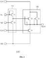
- FIG. 4 is a view of schematically illustrating the first GIP circuit according to the embodiment of the present disclosure.
- the first GIP circuit GIP1 includes a control unit 110 controlling a first node Q and an output unit 120 outputting the first gate signal Vout1 corresponding to the first clock signal CLK1 depending on a voltage state at the first node Q.
- control unit 110 controls the voltage state of the first node Q such that the first gate signal Vout1 corresponding to the first clock signal CLK1 is outputted from the output unit 120.
- control unit 110 includes a first transistor T1 connected between a start signal (Vst) input terminal and the first node Q and a second transistor T2 connected between the first node Q, a second gate signal Vg2 input terminal and a low level voltage VSS input terminal.
- drain and gate of the first transistor T1 are connected to each other, and the first transistor T1 functions as a diode. That is, a voltage at the drain of the first transistor T1 is inputted to source, and on the contrary to this, a voltage at the source is not inputted to the drain.
- the first transistor T1 applies the start signal Vst to the first node Q, and at the same time, the first transistor T1 prevents a voltage charged at the first node Q from being discharged to the outside through the first transistor T1.
- the second transistor T2 initializes the first node Q. At this time, the second transistor T2 turns on by the second gate signal Vg2 and charges the first node Q with the low level voltage VSS.
- the first node Q can be charged by the start signal Vst of a high level at the next frame.
- the output unit 120 outputs a high level of the first gate signal Vout1 or a low level of the first gate signal Vout1 depending on the voltage state of the first node Q.
- the output unit 120 includes a third transistor T3 connected between a first clock signal CLK1 input terminal, the first node Q and a first gate signal Vout1 output terminal, a fourth transistor T4 connected between a second clock signal CLK2 input terminal, the low level voltage VSS input terminal and source of the third transistor T3, a fifth transistor T5 connected between drain of the third transistor T3 and the first gate signal Vout1 output terminal, and a capacitor C connected between the first node Q and the source of the third transistor T3.
- the third transistor T3 turns on by a voltage of a high level charged at the first node Q and outputs the first gate signal Vout1 corresponding to a high level of the first clock signal CLK1.
- the first gate signal Vout1 is inputted to the second GIP circuit (not shown) as a starting signal. Then, the second GIP circuit outputs the second gate signal Vg2.
- the second gate signal Vg2 is inputted to the second gate signal Vg2 input terminal, and the second transistor T2 turns on by the second gate signal Vg2, whereby the first node Q is charged by the low level voltage VSS.
- source and gate of the fifth transistor T5 are connected to each other, and the fifth transistor T5 functions as a diode.
- the fifth transistor T5 turns on if the high level of the first clock signal is applied to the gate of the fifth transistor T5, and the fifth transistor T5 turns off if the low level voltage VSS is applied to the gate of the fifth transistor T5.
- the capacitor C is charged by a voltage level of the start signal Vst when the start signal Vst of the high level is inputted to the gate of the first transistor T1 and the first transistor T1 turns on.
- the fourth transistor T4 turns on by the second clock signal CLK2 and outputs the low level voltage VSS to the first gate signal Vout1 output terminal.
- the low level voltage VSS is charged at the first node Q by the second transistor T2, which turns on by the second gate signal Vg2, the third transistor T3 turns off, and initialization is accomplished.
- FIG. 5 is a view of a display panel including GIP circuits in a display area according to the embodiment of the present disclosure.
- second to seventh gate lines GL2 to GL7, first to fifth data lines DL1 to DL5 and one GIP circuit are shown in the figure.
- the GIP circuit corresponds to the sixth GIP circuit GIP6 of FIG. 2 wherein i is 6.
- two pixel columns are disposed between adjacent two of the first to fifth data lines DL1 to DL5, and two of the second to seventh gate lines GL2 to GL7 are disposed between adjacent two pixel rows.
- each pixel includes a pixel electrode P and a thin film transistor Tr.
- a data signal from one of the first to fifth data lines DL1 to DL5 is provided to two pixel columns, which are adjacent to each other with the one of the first to fifth data lines DL1 to DL5 therebetween.
- signal lines CLK, CLK2, VSS, Vst of FIG. 3 and Rst of FIG. 3 and transistors T1 to T5 which are included in the GIP circuit, are separately disposed between the two pixel columns and the next two pixel columns where there is no data line.
- the LCD device utilizes an area where the data lines DL1 to DL5 are not disposed in the display area AA. Accordingly, since it is not necessary to arrange an additional area for the signal lines CLK1, CLK2, VSS, Vst and Rst of FIG.3 and the transistors T1 to T5 in the display area AA, an aperture ratio can be prevented from being lowered.
- the signal lines CLK1, CLK2, VSS, Vst and Rst of FIG.3 include first and second clock signal lines CLK1 and CLK2, a start signal line Vst of FIG. 3 , a reset signal line Rst of FIG.3 , and a low level voltage line VSS.
- the GIP circuit further includes a first node line QL and a second node line (not shown). Each of the first node line QL and the second node line may be disposed between adjacent two pixel rows.
- the signal lines CLK1, CLK2, VSS, Vst and Rst of FIG.3 extend in the first direction, and may be formed of a same material on a same layer as the data lines DL1 to DL5.
- first node line QL and the second node line extend in the second direction. If the first node line QL and the second node line are spaced apart from the gate lines GL2 to GL7, the first node line QL and the second node line may be formed of the same material on the same layer as the gate lines GL2 to GL7. Alternatively, if the first node line QL and the second node line overlap the gate lines GL2 to GL7, the first node line QL and the second node line may be formed of a different material on a different layer from the gate lines GL2 to GL7.
- the transistors T1 to T5 include first to fifth transistors T1 to T5.
- gate and drain electrodes of the first transistor T1 are connected to the fifth gate line GL5, and a source electrode of the first transistor T1 is connected to the first node line QL.
- the first transistor T1 receives a gate signal supplied from the fifth gate line GL5 as a starting signal and inputs it to the first node line QL.
- the first transistor T1 of the first GIP circuit GIP1 of FIG. 3 cannot receive a gate signal outputted from the previous GIP circuit as a starting signal to start.
- the gate electrode of the first transistor T1 of the first GIP circuit GIP1 of FIG. 3 is connected to the start signal line Vst of FIG. 3 and receives a start signal supplied from the start signal line Vst of FIG. 3 to start.
- the gate and drain electrodes of the first transistor T1 are connected to each other, and the first transistor T1 functions as a diode. A voltage charged at the first node line QL is prevented from being discharged to the outside through the first transistor T 1.
- a drain electrode of the second transistor T2 is connected to the first node line QL, a source electrode of the second transistor T2 is connected to the low level voltage line VSS, and a gate electrode of the second transistor T2 is connected to the seventh gate line GL7.
- the second transistor T2 turns on by a gate signal supplied from the seventh gate line GL7 and inputs a low level voltage supplied from the low level voltage line VSS to the first node line QL.
- a next frame is prepared by charging the first node line QL with the low level voltage.
- a source electrode of the third transistor T3 is connected to the sixth gate line GL6, a drain electrode of the third transistor T3 is connected to the first clock signal line CLK1, and a gate electrode of the third transistor T3 is connected to the first node line QL.
- the third transistor T3 turns on by a high level voltage charged at the first node line QL and outputs a gate signal corresponding to the clock signal supplied from the first clock signal line CLK1 to the sixth gate line GL6.
- a gate electrode of the fourth transistor T4 is connected to the second clock signal line CLK2, a source electrode of the forth transistor T4 is connected to the low level voltage line VSS, and a drain electrode of the fourth transistor T4 is connected to the sixth gate line GL6 and the source electrode of the third transistor T3.
- the fourth transistor T4 turns on by a clock signal supplied from the second clock signal line CLK2 and outputs the low level voltage supplied from the low level voltage line VSS to the sixth gate line GL6.
- a drain electrode of the fifth transistor T5 is connected to the first clock signal line CLK1, and a gate electrode and a source electrode of the fifth transistor T5 are connected to the sixth gate line GL6 and the drain electrode of the third transistor T3.
- the fifth transistor T5 turns on a clock signal supplied from the first clock signal line CLK1 and outputs a gate signal corresponding to the clock signal to the sixth gate line GL6, and the fifth transistor T5 turn off by the low level voltage supplied from the low level voltage line VSS and outputs the low level voltage to the sixth gate line GL6.
- the gate and source electrodes of the fifth transistor T5 are connected to each other and the fifth transistor T5 functions as a diode.
- the sixth GIP circuit GIP6 of FIG. 3 outputs the gate signal to the sixth gate line GL6, the first to fifth transistors T1 to T5 of the sixth GIP circuit GIP6 of FIG. 3 are disposed between the fifth gate line GL5 and the sixth gate line GL6.
- the first transistor T1 is disposed at a left side of the first pixel column connected to the first data line DL1
- the second transistor T2 is disposed between two pixels P, which are located between the fourth and fifth data lines DL4 and DL5
- the third transistor T3 is disposed between the two pixels P, which are located between the first and second data lines DL1 and DL2
- the fourth transistor T4 is disposed between the two pixels P, which are located between the third and fourth data lines DL3 and DL4
- the fifth transistor T5 is disposed between the two pixels P, which are located between the second and third data lines DL2 and DL3.
- first clock signal line CLK1 is disposed between the two pixel columns, which are located between the first and second data lines DL1 and DL2, and also disposed between the two pixel columns, which are located between the second and third data lines DL2 and DL3.
- the first clock signal line CLK1 are connected to the third and fifth transistors T3 and T5.
- the second clock signal line CLK2 is disposed between the two pixel columns, which are located between the third and fourth data lines DL3 and DL4, and is connected to the fourth transistor T4.
- the low level voltage line VSS is disposed at a right side of the pixel column, which is located at a right side of the fifth data line DL5.
- the low level voltage line VSS extends parallel to the fourth and fifth gate lines GL4 and GL5 between the fourth and fifth gate lines GL4 and GL5 and is connected to the second and fourth transistors T2 and T4.
- the first node line QL is disposed parallel to the sixth and seventh gate lines GL6 and GL7 between the sixth and seventh gate lines GL6 and GL7 and is connected to the first, second and third transistors T1, T2 and T3.
- the number of the clock signals is not limited to this and is changeable.
- the gate line from which the first transistor T1 receives the starting signal and the gate line from which the second transistor T2 receives the gate signal to turn on may be changed.
- the first transistor T1 may receive the starting signal from the (i-4)th gate line, and the second transistor T2 may receive the gate signal of the (i+4)th gate line to turn on. That is, since i is 6, the gate electrode of the first transistor T1 may be connected to the second gate line, and the gate electrode of the second transistor T2 may be connected to the tenth gate line.
- the gate electrode of the first transistor T1 of each of the first to fourth GIP circuits may be connected to the start signal line Vst of FIG. 3
- the gate electrode of the second transistor T2 of each of the (j-3)th to (j)th GIP circuits may be connected to the reset signal line Rst of FIG. 3 .
- the narrow bezel can be achieved by disposing the signal lines CLK1, CLK2, VSS, Vst of FIG. 3 and Rst of FIG. 3 and the transistors T1 to T5 of the GIP circuits, which were disposed at the non-display areas NAA of FIG. 1 at the left and right sides of the display area AA of FIG. 1 , in the display area AA.
- the signal lines CLK1, CLK2, VSS, Vst of FIG. 3 and Rst of FIG. 3 and the transistors T1 to T5 of the GIP circuits are formed together when the data lines DL1 to DL5, the gate lines GL2 and GL7, and the thin film transistors Tr of the pixels P are formed, the manufacturing processes are simplified, and the manufacturing costs are decreased.
Landscapes
- Physics & Mathematics (AREA)
- Engineering & Computer Science (AREA)
- General Physics & Mathematics (AREA)
- Crystallography & Structural Chemistry (AREA)
- Chemical & Material Sciences (AREA)
- Theoretical Computer Science (AREA)
- Computer Hardware Design (AREA)
- Nonlinear Science (AREA)
- Mathematical Physics (AREA)
- Optics & Photonics (AREA)
- Microelectronics & Electronic Packaging (AREA)
- Devices For Indicating Variable Information By Combining Individual Elements (AREA)
- Liquid Crystal (AREA)
- Control Of Indicators Other Than Cathode Ray Tubes (AREA)
- Liquid Crystal Display Device Control (AREA)
Abstract
Description
- The present disclosure relates to a liquid crystal display device, and more particularly, to a liquid crystal display having a narrow bezel.
- A liquid crystal display (LCD) device includes a display panel, a data driving unit for providing data signals to data lines of the display panel, a gate driving unit for providing gate signals to gate lines of the display panel, and a timing controller for controlling the data driving unit and the gate driving unit.
- In the LCD device, the gate driving unit and the data driving unit are generally manufactured in an integrated circuit form and attached to the display panel in a TCP (tape carrier package) or COF (chip on film) type.
- Therefore, the number of components increases, and manufacturing processes and costs also rise due to an increase in the number of components. This causes a problem in decreasing a weight and size of the LCD device. To solve the problem, a GIP (gate in panel) type LCD device, in which the gate driving unit is formed in the display panel, has been suggested.
-
FIG. 1 is a plan view of a display panel of a GIP type LCD device according to a related art. - In
FIG. 1 , a display panel 10 of a GIP type LCD device according to the related art includes a display area AA and non-display areas NAA. The non-display areas NAA are disposed at outer sides of the display area AA, for example, at left and right sides of the display area AA, respectively. - Here, pixels P defined by gate lines GL and data lines DL crossing each other are disposed in the display area AA of the display panel 10, and GIP circuits each including signal lines (not shown) and transistors (not shown) are disposed in respective non-display areas NAA.
- Meantime, recently, in the LCD device, it is required to narrow a bezel, which is defined as a width of the non-display area NAA, with pursuing a light weight and thin thickness for a slim design of a final product such as monitors or TVs.
- However, as stated above, in the GIP type LCD device according to the related art, since the GIP circuits GIP, each of which includes the signal lines (not shown) and the transistors (not shown), are formed in the non-display areas NAA at left and right sides of the display area AA, there is a limitation on achieving a narrow bezel.
- Accordingly, the present disclosure is directed to an LCD device that substantially obviates one or more of the problems due to limitations and disadvantages of the related art.
- An object of the present disclosure is to provide an LCD device that has a narrow bezel by disposing signal lines and transistors of a GIP circuit.
- Additional features and advantages of the invention will be set forth in the description which follows, and in part will be apparent from the description, or may be learned by practice of the invention. The objectives and other advantages of the invention will be realized and attained by the structure particularly pointed out in the written description and claims hereof as well as the appended drawings. The objects are solved by the features of the independent claim.
- According to one aspect, there is provided a liquid crystal display device including a display panel including a display area and a non-display area, wherein in the display area, m/2 (m is a positive even number) data lines of a first direction and 2n (n is an integer more than 5) gate lines of a second direction cross each other to thereby define m × n pixels; and 2n GIP circuits in the display area and each including signal lines and transistors, wherein two gate lines are disposed between adjacent two pixel rows, and two pixel columns are disposed between adjacent two data lines, and wherein the signal lines and the transistors are separately disposed between the two pixel columns. Preferably, odd GIP circuits of the GIP circuits output odd gate lines of the gate lines, and even GIP circuits of the GIP circuits output even gate lines of the gate lines. Preferably, the signal lines include at least one of first and second clock signal lines, a start signal line, a reset signal line and a low level voltage line. Preferably, the signal lines are disposed on a same layer as the data lines. Preferably, the GIP circuit further includes first and second node lines. The first and second node lines may be disposed between adjacent two pixel rows. Preferably, the first and second node lines are spaced apart from the gate lines. Preferably, the first and second node lines are disposed on a same layer as the gate lines. Preferably, the first and second node lines overlap the gate lines. Preferably, the first and second node lines are disposed on a different layer from the gate lines. Preferably, the transistors include at least one of: a first transistor connected to the start signal line and the first node line; a second transistor connected to the first node line and the low level voltage line; a third transistor connected to the first clock signal line and the first node line; a fourth transistor connected to the second clock signal line, the low level voltage line and the third transistor; and a fifth transistor connected to the first clock signal line and the third transistor. Preferably, the liquid crystal display device further comprises a data driving unit in the non-display area and outputting data signals to the data lines.
- It is to be understood that both the foregoing general description and the following detailed description are exemplary and explanatory and are intended to provide further explanation of the invention as claimed.
- The accompanying drawings, which are included to provide a further understanding of the invention and are incorporated in and constitute a part of this specification, illustrate embodiments of the invention and together with the description serve to explain the principles of the invention. In the drawings:
-
FIG. 1 is a plan view of a display panel of a GIP type LCD device according to a related art; -
FIG. 2 is a plan view of a display panel of a GIP type LCD device according to an embodiment of the present disclosure; -
FIG. 3 is a schematic view of illustrating a plurality of GIP circuits according to the embodiment of the present disclosure; -
FIG. 4 is a view of schematically illustrating the first GIP circuit according to the embodiment of the present disclosure; and -
FIG. 5 is a view of a display panel including GIP circuits in a display area according to the embodiment of the present disclosure. - Reference will now be made in detail to the embodiment of the disclosure, an example of which is illustrated in the accompanying drawings.
-
FIG. 2 is a plan view of a display panel of a GIP type LCD device according to an embodiment of the present disclosure. - In
FIG. 2 , thedisplay panel 100 of a GIP type LCD device according to the embodiment of the present disclosure includes a display area AA and non-display areas (not shown) at outer sides of the display area AA. - More specifically, a plurality of pixels (not shown), which are defined by a plurality of gate lines GL1 to GL6 and a plurality of data lines (not shown) crossing each other, are disposed in the display area AA of the
display panel 100. - Particularly, a plurality of GIP circuits GIP1 to GIP6, each of which includes a plurality of signal lines (not shown) and a plurality of transistors (not shown), are disposed in the display area AA of the
display panel 100. - In the embodiment of the present disclosure, a narrow bezel can be achieved by disposing the GIP circuits GIP1 to GIP6 in the display area AA while the GIP circuits are disposed in the non-display areas NAA of
FIG. 1 at the left and right sides of the display area AA ofFIG. 1 in the LCD device according to the related art. This will be described in more detail later. - Meanwhile, although more gate lines and GIP circuits may be disposed in the display area AA of the
display panel 100, for convenience of explanation, six gate lines GL1 to GL6 and six GIP circuits GIP1 to GIP6 are shown in the figure. - At this time, odd GIP circuits GIP1, GIP3 and GIP5 of the GIP circuits GIP1 to GIP6 output gate signals to odd gate lines GL1, GL3 and GL5 of the gate lines GL1 to GL6, respectively, and even GIP circuits GIP2, GIP4 and GIP6 of the GIP circuits GIP1 to GIP6 output gate signals to even gate lines GL2, GL4 and GL6 of the gate lines GL1 to GL6, respectively.
- In the meantime, although not shown in the figure, a data driving unit (not shown) may be further disposed in the non-display area (not shown) at an upper or lower side of the display area AA.
- At this time, the data driving unit (not shown) outputs data signals to the data lines (not shown) in the display area AA.
-
FIG. 3 is a schematic view of illustrating a plurality of GIP circuits according to the embodiment of the present disclosure. - In
FIG. 3 , the GIP circuits GIP1, ..., GIP(i-1), GIP(i), GIP(i+1), ..., and GIP(j) respectively output gate signals Vout1, ..., Vout(i-1), Vout(i), Vout(i+1), ..., and Vout(j), each of which has one high level during a frame, wherein i is an integer larger than 2, and j is an integer larger than 4. - At this time, first GIP circuit to (j)th GIP circuit GIP1 to GIP(j) each receive at least one of a plurality of clock signals CLK1 and CLK2 and sequentially output the gate signals Vout1, ..., Vout(i-1), Vout(i), Vout(i+1), ..., and Vout(j) having the high level to the gate lines GL1, ..., GL(i-1), GL(i), GL(i+1), ..., and GL(j), respectively, wherein i is an integer larger than 2, and j is an integer larger than 4.
- In addition, each of the plurality of clock signals CLK1 and CLK2 partially overlaps the next clock signal, and the plurality of clock signals CLK1 and CLK2 are sequentially and repeatedly applied to the GIP circuits GIP1, ..., GIP(i-1), GIP(i), GIP(i+1), ..., and GIP(j). For example, each of the plurality of clock signals CLK1 and CLK2 may overlap 2/3 of a high level section of the next clock signal. Here, although two clock signals CLK1 and CLK2 are used, the number of clock signals CLK1 and CLK2 are not limited to this.
- The gate signals Vout1, ..., Vout(i-1), Vout(i), Vout(i+1), ..., and Vout(j), which are respectively outputted from the GIP circuits GIP1, ..., GIP(i-1), GIP(i), GIP(i+1), ..., and GIP(j), are sequentially provided to the gate lines GL1, ..., GL(i-1), GL(i), GL(i+1), ..., and GL(j) of a display panel (not shown) displaying images.
- More specifically, the first GIP circuit GIP1 outputs the first gate signal Vout1 having the high level to the first gate line GL1, ..., the (i-1)th GIP circuit GIP(i-1) outputs the (i-1)th gate signal Vout(i-1) having the high level to the (i-1)th gate line GL(i-1), the (i)th GIP circuit GIP(i) outputs the (i)th gate signal Vout(i) having the high level to the (i)th gate line GL(i), the (i+1)th GIP circuit GIP(i+1) outputs the (i+1)th gate signal Vout(i+1) having the high level to the (i+1)th gate line GL(i+1), ..., and the (j)th GIP circuit GIP(j) outputs the (j)th gate signal Vout(j) having the high level to the (j)th gate line GL(j).
- First, since there is no previous GIP circuit before the first GIP circuit GIP1, the first GIP circuit GIP1 cannot receive a gate signal of the previous GIP circuit as a starting signal to start. Thus, the first GIP circuit GIP1 receives a start signal Vst and starts.
- Accordingly, the start signal Vst is applied to the first GIP circuit GIP1, the first GIP circuit GIP1 outputs the first gate signal Vout1 of the high level using the first clock signal CLK1, ..., the (i-1)th gate signal Vout(i-1) of the high level outputted from the (i-1)th GIP circuit GIP(i-1) is provided to the (i)th GIP circuit GIP(i) to thereby start the (i)th GIP circuit GIP(i), and the (i)th GIP circuit GIP(i) outputs the (i)th gate signal Vout(i) of the high level using the second clock signal CLK2 (in the figure, although the second clock signal CLK2 is used, the first clock signal CLK1 or another clock signal may be used).
- Next, the (i)th gate signal Vout(i) of the high level outputted from the (i)th GIP circuit GIP(i) is provided to the (i+1)th GIP circuit GIP(i+1) to thereby start the (i+1)th GIP circuit GIP(i+1), and the (i+1)th GIP circuit GIP(i+1) outputs the (i+1)th gate signal Vout(i+1) of the high level using the first clock signal CLK1 (in the figure, although the first clock signal CLK1 is used, the first clock signal CLK1 or another clock signal may be used), ..., the (j)th GIP circuit GIP(j) outputs the (j)th gate signal Vout(j) of the high level using the second clock signal CLK2 (in the figure, although the second clock signal CLK2 is used, the first clock signal CLK1 or another clock signal may be used).
- When the (j)th gate signal Vout(j) is outputted from the (j)th GIP circuit GIP(j) where one frame ends, the (j)th GIP circuit GIP(j) receives a reset signal Rst and is initialized such that the first gate signal Vout1 is outputted from the first GIP circuit GIP1 where the next frame starts.
-
FIG. 4 is a view of schematically illustrating the first GIP circuit according to the embodiment of the present disclosure. - In
FIG. 4 , the first GIP circuit GIP1 includes acontrol unit 110 controlling a first node Q and anoutput unit 120 outputting the first gate signal Vout1 corresponding to the first clock signal CLK1 depending on a voltage state at the first node Q. - Here, the
control unit 110 controls the voltage state of the first node Q such that the first gate signal Vout1 corresponding to the first clock signal CLK1 is outputted from theoutput unit 120. - To do this, the
control unit 110 includes a first transistor T1 connected between a start signal (Vst) input terminal and the first node Q and a second transistor T2 connected between the first node Q, a second gate signal Vg2 input terminal and a low level voltage VSS input terminal. - Here, drain and gate of the first transistor T1 are connected to each other, and the first transistor T1 functions as a diode. That is, a voltage at the drain of the first transistor T1 is inputted to source, and on the contrary to this, a voltage at the source is not inputted to the drain.
- Therefore, the first transistor T1 applies the start signal Vst to the first node Q, and at the same time, the first transistor T1 prevents a voltage charged at the first node Q from being discharged to the outside through the first transistor T1.
- In addition, the second transistor T2 initializes the first node Q. At this time, the second transistor T2 turns on by the second gate signal Vg2 and charges the first node Q with the low level voltage VSS.
- According to this, the first node Q can be charged by the start signal Vst of a high level at the next frame.
- The
output unit 120 outputs a high level of the first gate signal Vout1 or a low level of the first gate signal Vout1 depending on the voltage state of the first node Q. - To do this, the
output unit 120 includes a third transistor T3 connected between a first clock signal CLK1 input terminal, the first node Q and a first gate signal Vout1 output terminal, a fourth transistor T4 connected between a second clock signal CLK2 input terminal, the low level voltage VSS input terminal and source of the third transistor T3, a fifth transistor T5 connected between drain of the third transistor T3 and the first gate signal Vout1 output terminal, and a capacitor C connected between the first node Q and the source of the third transistor T3. - At this time, the third transistor T3 turns on by a voltage of a high level charged at the first node Q and outputs the first gate signal Vout1 corresponding to a high level of the first clock signal CLK1.
- Additionally, the first gate signal Vout1 is inputted to the second GIP circuit (not shown) as a starting signal. Then, the second GIP circuit outputs the second gate signal Vg2.
- Moreover, the second gate signal Vg2 is inputted to the second gate signal Vg2 input terminal, and the second transistor T2 turns on by the second gate signal Vg2, whereby the first node Q is charged by the low level voltage VSS.
- Furthermore, source and gate of the fifth transistor T5 are connected to each other, and the fifth transistor T5 functions as a diode. At this time, the fifth transistor T5 turns on if the high level of the first clock signal is applied to the gate of the fifth transistor T5, and the fifth transistor T5 turns off if the low level voltage VSS is applied to the gate of the fifth transistor T5.
- In addition, the capacitor C is charged by a voltage level of the start signal Vst when the start signal Vst of the high level is inputted to the gate of the first transistor T1 and the first transistor T1 turns on.
- Then, when the capacitor C is charged with a voltage more than a threshold voltage between the gate and source of the third transistor T3 and the first clock signal CLK1 is high, bootstrapping occurs. A voltage larger than the high level of the start signal Vst is charged at the first node Q, and the voltage of the first node Q is definitely high. Thus, the third transistor T3 turns on.
- Moreover, the fourth transistor T4 turns on by the second clock signal CLK2 and outputs the low level voltage VSS to the first gate signal Vout1 output terminal.
- At this time, the low level voltage VSS is charged at the first node Q by the second transistor T2, which turns on by the second gate signal Vg2, the third transistor T3 turns off, and initialization is accomplished.
- These processes are repeatedly performed at each frame.
-
FIG. 5 is a view of a display panel including GIP circuits in a display area according to the embodiment of the present disclosure. - In the display area AA of the
display panel 100, m/2 (m is a positive even number) data lines extending in a first direction and 2n (n is an integer more than 5) gate lines extending in a second direction cross each other to thereby define m × n pixels, and 2n GIP circuits are disposed. However, for convenience of explanation, second to seventh gate lines GL2 to GL7, first to fifth data lines DL1 to DL5 and one GIP circuit are shown in the figure. At this time, the GIP circuit corresponds to the sixth GIP circuit GIP6 ofFIG. 2 wherein i is 6. - In
FIG. 5 , two pixel columns are disposed between adjacent two of the first to fifth data lines DL1 to DL5, and two of the second to seventh gate lines GL2 to GL7 are disposed between adjacent two pixel rows. - In addition, each pixel includes a pixel electrode P and a thin film transistor Tr. A data signal from one of the first to fifth data lines DL1 to DL5 is provided to two pixel columns, which are adjacent to each other with the one of the first to fifth data lines DL1 to DL5 therebetween.
- At this time, there is no data line between the two pixel columns, which are adjacent to each other with the one of the first to fifth data lines DL1 to DL5 therebetween, and the next two pixel columns.
- Here, signal lines CLK, CLK2, VSS, Vst of
FIG. 3 and Rst ofFIG. 3 and transistors T1 to T5, which are included in the GIP circuit, are separately disposed between the two pixel columns and the next two pixel columns where there is no data line. - Namely, the LCD device according to the present invention utilizes an area where the data lines DL1 to DL5 are not disposed in the display area AA. Accordingly, since it is not necessary to arrange an additional area for the signal lines CLK1, CLK2, VSS, Vst and Rst of
FIG.3 and the transistors T1 to T5 in the display area AA, an aperture ratio can be prevented from being lowered. - At this time, the signal lines CLK1, CLK2, VSS, Vst and Rst of
FIG.3 include first and second clock signal lines CLK1 and CLK2, a start signal line Vst ofFIG. 3 , a reset signal line Rst ofFIG.3 , and a low level voltage line VSS. - In addition, the GIP circuit further includes a first node line QL and a second node line (not shown). Each of the first node line QL and the second node line may be disposed between adjacent two pixel rows.
- Meanwhile, the signal lines CLK1, CLK2, VSS, Vst and Rst of
FIG.3 extend in the first direction, and may be formed of a same material on a same layer as the data lines DL1 to DL5. - Moreover, the first node line QL and the second node line extend in the second direction. If the first node line QL and the second node line are spaced apart from the gate lines GL2 to GL7, the first node line QL and the second node line may be formed of the same material on the same layer as the gate lines GL2 to GL7. Alternatively, if the first node line QL and the second node line overlap the gate lines GL2 to GL7, the first node line QL and the second node line may be formed of a different material on a different layer from the gate lines GL2 to GL7.
- Furthermore, the transistors T1 to T5 include first to fifth transistors T1 to T5.
- More specifically, gate and drain electrodes of the first transistor T1 are connected to the fifth gate line GL5, and a source electrode of the first transistor T1 is connected to the first node line QL.
- At this time, the first transistor T1 receives a gate signal supplied from the fifth gate line GL5 as a starting signal and inputs it to the first node line QL.
- In the meantime, since there is no previous GIP circuit before the first GIP circuit GIP1 of
FIG. 3 , the first transistor T1 of the first GIP circuit GIP1 ofFIG. 3 cannot receive a gate signal outputted from the previous GIP circuit as a starting signal to start. Thus, the gate electrode of the first transistor T1 of the first GIP circuit GIP1 ofFIG. 3 is connected to the start signal line Vst ofFIG. 3 and receives a start signal supplied from the start signal line Vst ofFIG. 3 to start. - In addition, the gate and drain electrodes of the first transistor T1 are connected to each other, and the first transistor T1 functions as a diode. A voltage charged at the first node line QL is prevented from being discharged to the outside through the
first transistor T 1. - Moreover, a drain electrode of the second transistor T2 is connected to the first node line QL, a source electrode of the second transistor T2 is connected to the low level voltage line VSS, and a gate electrode of the second transistor T2 is connected to the seventh gate line GL7.
- At this time, the second transistor T2 turns on by a gate signal supplied from the seventh gate line GL7 and inputs a low level voltage supplied from the low level voltage line VSS to the first node line QL.
- Like this, a next frame is prepared by charging the first node line QL with the low level voltage.
- Additionally, a source electrode of the third transistor T3 is connected to the sixth gate line GL6, a drain electrode of the third transistor T3 is connected to the first clock signal line CLK1, and a gate electrode of the third transistor T3 is connected to the first node line QL.
- At this time, the third transistor T3 turns on by a high level voltage charged at the first node line QL and outputs a gate signal corresponding to the clock signal supplied from the first clock signal line CLK1 to the sixth gate line GL6.
- In the meantime, as stated above, if the low level voltage is charged at the first node line QL by the second transistor T2 turning on, the third transistor T3 turns on, and the initialization is accomplished.
- In addition, a gate electrode of the fourth transistor T4 is connected to the second clock signal line CLK2, a source electrode of the forth transistor T4 is connected to the low level voltage line VSS, and a drain electrode of the fourth transistor T4 is connected to the sixth gate line GL6 and the source electrode of the third transistor T3.
- At this time, the fourth transistor T4 turns on by a clock signal supplied from the second clock signal line CLK2 and outputs the low level voltage supplied from the low level voltage line VSS to the sixth gate line GL6.
- Moreover, a drain electrode of the fifth transistor T5 is connected to the first clock signal line CLK1, and a gate electrode and a source electrode of the fifth transistor T5 are connected to the sixth gate line GL6 and the drain electrode of the third transistor T3.
- At this time, the fifth transistor T5 turns on a clock signal supplied from the first clock signal line CLK1 and outputs a gate signal corresponding to the clock signal to the sixth gate line GL6, and the fifth transistor T5 turn off by the low level voltage supplied from the low level voltage line VSS and outputs the low level voltage to the sixth gate line GL6.
- Meanwhile, the gate and source electrodes of the fifth transistor T5 are connected to each other and the fifth transistor T5 functions as a diode.
- In the above processes, although it is explained to output a gate signal from a sixth GIP circuit GIP6 of
FIG. 3 disposed in the display area AA to the sixth gate line GL6, other GIP circuits may output gate signals to respective gate lines according to the same processes as the above processes. - Hereinafter, arrangement structures and connection relations of the first to fifth transistors T1 to T5, the signal lines CLK1, CLK2 and VSS connected to the first to fifth transistors T1 to T5, and the first node line QL will be explained with reference to
FIG. 5 . - First, since the sixth GIP circuit GIP6 of
FIG. 3 outputs the gate signal to the sixth gate line GL6, the first to fifth transistors T1 to T5 of the sixth GIP circuit GIP6 ofFIG. 3 are disposed between the fifth gate line GL5 and the sixth gate line GL6. - At this time, the first transistor T1 is disposed at a left side of the first pixel column connected to the first data line DL1, the second transistor T2 is disposed between two pixels P, which are located between the fourth and fifth data lines DL4 and DL5, the third transistor T3 is disposed between the two pixels P, which are located between the first and second data lines DL1 and DL2, the fourth transistor T4 is disposed between the two pixels P, which are located between the third and fourth data lines DL3 and DL4, and the fifth transistor T5 is disposed between the two pixels P, which are located between the second and third data lines DL2 and DL3.
- In addition, the first clock signal line CLK1 is disposed between the two pixel columns, which are located between the first and second data lines DL1 and DL2, and also disposed between the two pixel columns, which are located between the second and third data lines DL2 and DL3.
- At this time, the first clock signal line CLK1 are connected to the third and fifth transistors T3 and T5.
- Moreover, the second clock signal line CLK2 is disposed between the two pixel columns, which are located between the third and fourth data lines DL3 and DL4, and is connected to the fourth transistor T4.
- Furthermore, the low level voltage line VSS is disposed at a right side of the pixel column, which is located at a right side of the fifth data line DL5.
- At this time, the low level voltage line VSS extends parallel to the fourth and fifth gate lines GL4 and GL5 between the fourth and fifth gate lines GL4 and GL5 and is connected to the second and fourth transistors T2 and T4.
- Additionally, the first node line QL is disposed parallel to the sixth and seventh gate lines GL6 and GL7 between the sixth and seventh gate lines GL6 and GL7 and is connected to the first, second and third transistors T1, T2 and T3.
- In the above embodiment, two clock signals are used. However, the number of the clock signals is not limited to this and is changeable.
- Meanwhile, the gate line from which the first transistor T1 receives the starting signal and the gate line from which the second transistor T2 receives the gate signal to turn on may be changed.
- For example, when eight clock signals are used, the first transistor T1 may receive the starting signal from the (i-4)th gate line, and the second transistor T2 may receive the gate signal of the (i+4)th gate line to turn on. That is, since i is 6, the gate electrode of the first transistor T1 may be connected to the second gate line, and the gate electrode of the second transistor T2 may be connected to the tenth gate line.
- At this time, the gate electrode of the first transistor T1 of each of the first to fourth GIP circuits may be connected to the start signal line Vst of
FIG. 3 , and the gate electrode of the second transistor T2 of each of the (j-3)th to (j)th GIP circuits may be connected to the reset signal line Rst ofFIG. 3 . - Like this, the narrow bezel can be achieved by disposing the signal lines CLK1, CLK2, VSS, Vst of
FIG. 3 and Rst ofFIG. 3 and the transistors T1 to T5 of the GIP circuits, which were disposed at the non-display areas NAA ofFIG. 1 at the left and right sides of the display area AA ofFIG. 1 , in the display area AA. - In addition, since the signal lines CLK1, CLK2, VSS, Vst of
FIG. 3 and Rst ofFIG. 3 and the transistors T1 to T5 of the GIP circuits are formed together when the data lines DL1 to DL5, the gate lines GL2 and GL7, and the thin film transistors Tr of the pixels P are formed, the manufacturing processes are simplified, and the manufacturing costs are decreased. - It will be apparent to those skilled in the art that various modifications and variations can be made in a display device of the present disclosure without departing from the scope of the invention. Thus, it is intended that the present disclosure covers the modifications and variations of this invention provided they come within the scope of the appended claims and their equivalents.
Claims (15)
- A liquid crystal display device comprising:a display panel including a display area with m × n pixels and a non-display area,m/2 data lines arranged in the display area in a first direction, with m being a positive even number,2n gate lines arranged in the display area in a second direction, with n being an integer more than 5, wherein the gate lines and the data lines cross each other for defining the m × n pixels arranged in m pixel columns and n pixel rows; and2n GIP circuits arranged in the display area, the GIP circuit including transistors,wherein two gate lines are disposed between adjacent two pixel rows, and two pixel columns are disposed between adjacent two data lines, and
wherein the transistors are arranged between pixel columns disposed between adjacent two data lines. - The liquid crystal display device of claim 1, wherein output of odd GIP circuits of the 2n GIP circuits is provided to odd gate lines of the 2n gate lines, and output of even GIP circuits of the 2n GIP circuits is provided to even gate lines of the 2n gate lines.
- The liquid crystal display device of claim 1 or 2, further including signal lines for providing signals to the GIP circuits, the signal lines being arranged between pixel columns disposed between adjacent two data lines.
- The liquid crystal display device of claim 3, wherein the signal lines are disposed on a same layer as the data lines and/or are made of a same material as the data lines.
- The liquid crystal display device according to any one of the preceding claims 3 or 4, wherein the signal lines extend in the first direction.
- The liquid crystal display device according to any one of the preceding claims, wherein the GIP circuit further includes at least one of a first and second node lines disposed between adjacent two pixel rows.
- The liquid crystal display device of claim 6, wherein at least one of the first and second node lines is spaced apart from the gate lines and/or is disposed on a same layer as the gate lines and/or is made of a same material as the gate lines.
- The liquid crystal display device of claim 6, wherein at least one of the first and second node lines is arranged overlapping one of the gate lines and is disposed on a different layer from the gate lines.
- The liquid crystal display device according to any one of the preceding claims 6 to 8, wherein the first and/or second node lines extend in the second direction.
- The liquid crystal display device according to any one of the preceding claims 3 to 9, wherein the signal lines include first and second clock signal lines, a start signal line, a reset signal line and a low level voltage line.
- The liquid crystal display device of claim 10, wherein a first GIP circuit configured to output a gate signal to a first gate line includes:a first transistor connected to the start signal line and the first node line;a second transistor connected to the first node line and the low level voltage line;a third transistor connected to the first clock signal line and the first node line;a fourth transistor connected to the second clock signal line, the low level voltage line and the third transistor; anda fifth transistor connected to the first clock signal line and the third transistor.
- The liquid crystal display device of claim 10 or 11, wherein an ith GIP circuit configured to output a gate signal to an ith gate line, with i being an integer larger than 2, includes:a first transistor connected to a (i-1)th gate line and the first node line;a second transistor connected to the first node line and the low level voltage line;a third transistor connected to the first clock signal line and the first node line;a fourth transistor connected to the second clock signal line, the low level voltage line and the third transistor; anda fifth transistor connected to the first clock signal line and the third transistor.
- The liquid crystal display device according to any one of the preceding claims, wherein each transistor of one GIP circuit is arranged between two pixel columns that are disposed between adjacent two data lines and/or wherein the transistors of one GIP circuit are arranged in the second direction along one of the gate lines.
- The liquid crystal display device according to any one of the preceding claims, further comprising a data driving unit in the non-display area and configured to output data signals to the data lines.
- The liquid crystal display device according to any one of the preceding claims, wherein two pixels of one pixel row are connected to a same data line arranged therebetween and/or wherein pixels of one pixel row are alternately connected to an odd and an even gate line.
Applications Claiming Priority (1)
| Application Number | Priority Date | Filing Date | Title |
|---|---|---|---|
| KR1020150190179A KR102481785B1 (en) | 2015-12-30 | 2015-12-30 | Liquid crystal display device |
Publications (2)
| Publication Number | Publication Date |
|---|---|
| EP3193325A1 true EP3193325A1 (en) | 2017-07-19 |
| EP3193325B1 EP3193325B1 (en) | 2020-11-11 |
Family
ID=57777468
Family Applications (1)
| Application Number | Title | Priority Date | Filing Date |
|---|---|---|---|
| EP16207554.3A Active EP3193325B1 (en) | 2015-12-30 | 2016-12-30 | Liquid crystal display device |
Country Status (5)
| Country | Link |
|---|---|
| US (1) | US10176775B2 (en) |
| EP (1) | EP3193325B1 (en) |
| JP (1) | JP6431028B2 (en) |
| KR (1) | KR102481785B1 (en) |
| CN (1) | CN106932936B (en) |
Cited By (2)
| Publication number | Priority date | Publication date | Assignee | Title |
|---|---|---|---|---|
| EP3187928A3 (en) * | 2015-12-31 | 2017-11-01 | LG Display Co., Ltd. | Display device |
| EP3477626A3 (en) * | 2017-10-26 | 2019-06-12 | LG Display Co., Ltd. | Oled display panel and oled display device |
Families Citing this family (15)
| Publication number | Priority date | Publication date | Assignee | Title |
|---|---|---|---|---|
| KR20190010052A (en) * | 2017-07-20 | 2019-01-30 | 엘지전자 주식회사 | Display device |
| JP2019074583A (en) * | 2017-10-13 | 2019-05-16 | シャープ株式会社 | Display device |
| KR102416888B1 (en) * | 2017-10-19 | 2022-07-04 | 엘지디스플레이 주식회사 | Display panel |
| KR102467881B1 (en) * | 2017-11-27 | 2022-11-16 | 엘지디스플레이 주식회사 | OLED display Panel |
| TWI677864B (en) * | 2018-06-28 | 2019-11-21 | 友達光電股份有限公司 | Display device |
| CN109064907A (en) * | 2018-10-24 | 2018-12-21 | 昆山国显光电有限公司 | Display panel and display device |
| TWI738281B (en) * | 2020-04-01 | 2021-09-01 | 友達光電股份有限公司 | Display panel |
| CN111429828A (en) | 2020-04-13 | 2020-07-17 | 深圳市华星光电半导体显示技术有限公司 | Display panel and display device |
| CN114067756B (en) * | 2020-07-30 | 2024-04-16 | 乐金显示有限公司 | Display device |
| WO2022133830A1 (en) | 2020-12-23 | 2022-06-30 | 京东方科技集团股份有限公司 | Display panel and display apparatus |
| KR102832919B1 (en) * | 2021-03-16 | 2025-07-11 | 삼성디스플레이 주식회사 | Display device and tiled display device including the same |
| CN113703236B (en) * | 2021-08-18 | 2023-05-02 | Tcl华星光电技术有限公司 | Display panel and array substrate thereof |
| KR102846695B1 (en) * | 2021-09-01 | 2025-08-13 | 엘지디스플레이 주식회사 | Display panel compensation circuit and display device including same |
| CN115050301B (en) * | 2022-06-30 | 2024-08-30 | 厦门天马显示科技有限公司 | Display panel and display device |
| CN115311981B (en) * | 2022-08-29 | 2025-09-02 | 武汉天马微电子有限公司 | Display panel and display device |
Citations (3)
| Publication number | Priority date | Publication date | Assignee | Title |
|---|---|---|---|---|
| EP1492078A2 (en) * | 2003-06-23 | 2004-12-29 | Samsung Electronics Co., Ltd. | Display driving device with partitioned gate driving unit and liquid crystal display apparatus and method using the same |
| US20140043306A1 (en) * | 2012-08-10 | 2014-02-13 | Lg Display Co., Ltd. | Liquid crystal display device |
| CN104849928A (en) * | 2015-04-16 | 2015-08-19 | 上海中航光电子有限公司 | TFT array substrate, display panel and display device |
Family Cites Families (18)
| Publication number | Priority date | Publication date | Assignee | Title |
|---|---|---|---|---|
| US5473270A (en) * | 1993-05-28 | 1995-12-05 | At&T Corp. | Adiabatic dynamic precharge boost circuitry |
| JPH08212188A (en) | 1995-02-01 | 1996-08-20 | Toshiba Corp | Cause / effect graph creation device and sentence type classification device |
| KR100589324B1 (en) | 2004-05-11 | 2006-06-14 | 삼성에스디아이 주식회사 | Light emitting display device and driving method thereof |
| JP4932415B2 (en) | 2006-09-29 | 2012-05-16 | 株式会社半導体エネルギー研究所 | Semiconductor device |
| EP2447950A1 (en) | 2009-06-25 | 2012-05-02 | Sharp Kabushiki Kaisha | Shift register circuit, display device provided with same, and shift register circuit driving method |
| JP2011170300A (en) | 2010-02-22 | 2011-09-01 | Hitachi Displays Ltd | Control circuit for display device |
| KR102022698B1 (en) * | 2012-05-31 | 2019-11-05 | 삼성디스플레이 주식회사 | Display panel |
| KR101991675B1 (en) * | 2012-08-10 | 2019-06-25 | 엘지디스플레이 주식회사 | Liquid crystal display device |
| JP5956600B2 (en) * | 2012-10-30 | 2016-07-27 | シャープ株式会社 | Active matrix substrate, display panel and display device including the same |
| CN103761944B (en) * | 2013-12-25 | 2017-01-25 | 合肥京东方光电科技有限公司 | Gate drive circuit, display device and drive method |
| KR102306098B1 (en) * | 2014-03-10 | 2021-09-28 | 엘지디스플레이 주식회사 | Display device and method of drving the same |
| JPWO2015163306A1 (en) * | 2014-04-22 | 2017-04-20 | シャープ株式会社 | Active matrix substrate and display device including the same |
| CN106233366A (en) * | 2014-04-22 | 2016-12-14 | 夏普株式会社 | Active matrix substrate and display device having same |
| CN106233368B (en) * | 2014-04-28 | 2019-03-12 | 夏普株式会社 | display device |
| JPWO2015166857A1 (en) * | 2014-04-28 | 2017-04-20 | シャープ株式会社 | Active matrix substrate and display device including the same |
| WO2016039184A1 (en) * | 2014-09-12 | 2016-03-17 | シャープ株式会社 | Display device |
| CN107003581B (en) * | 2014-11-21 | 2020-11-13 | 夏普株式会社 | Active matrix substrate and display panel |
| JPWO2016080542A1 (en) * | 2014-11-21 | 2017-08-31 | シャープ株式会社 | Active matrix substrate and display panel |
-
2015
- 2015-12-30 KR KR1020150190179A patent/KR102481785B1/en active Active
-
2016
- 2016-12-28 CN CN201611235575.7A patent/CN106932936B/en active Active
- 2016-12-28 JP JP2016254586A patent/JP6431028B2/en active Active
- 2016-12-28 US US15/392,097 patent/US10176775B2/en active Active
- 2016-12-30 EP EP16207554.3A patent/EP3193325B1/en active Active
Patent Citations (4)
| Publication number | Priority date | Publication date | Assignee | Title |
|---|---|---|---|---|
| EP1492078A2 (en) * | 2003-06-23 | 2004-12-29 | Samsung Electronics Co., Ltd. | Display driving device with partitioned gate driving unit and liquid crystal display apparatus and method using the same |
| US20140043306A1 (en) * | 2012-08-10 | 2014-02-13 | Lg Display Co., Ltd. | Liquid crystal display device |
| CN104849928A (en) * | 2015-04-16 | 2015-08-19 | 上海中航光电子有限公司 | TFT array substrate, display panel and display device |
| US20160307937A1 (en) * | 2015-04-16 | 2016-10-20 | Shanghai Avic Opto Electronics Co., Ltd. | Thin-film transistor, array substrate and display apparatus |
Cited By (3)
| Publication number | Priority date | Publication date | Assignee | Title |
|---|---|---|---|---|
| EP3187928A3 (en) * | 2015-12-31 | 2017-11-01 | LG Display Co., Ltd. | Display device |
| EP3477626A3 (en) * | 2017-10-26 | 2019-06-12 | LG Display Co., Ltd. | Oled display panel and oled display device |
| US10692439B2 (en) | 2017-10-26 | 2020-06-23 | Lg Display Co., Ltd. | OLED display panel and OLED display device |
Also Published As
| Publication number | Publication date |
|---|---|
| KR20170079509A (en) | 2017-07-10 |
| KR102481785B1 (en) | 2022-12-26 |
| JP2017120426A (en) | 2017-07-06 |
| JP6431028B2 (en) | 2018-11-28 |
| US20170193939A1 (en) | 2017-07-06 |
| CN106932936A (en) | 2017-07-07 |
| US10176775B2 (en) | 2019-01-08 |
| EP3193325B1 (en) | 2020-11-11 |
| CN106932936B (en) | 2020-09-01 |
Similar Documents
| Publication | Publication Date | Title |
|---|---|---|
| EP3193325B1 (en) | Liquid crystal display device | |
| EP3685223B1 (en) | Array substrate and display apparatus | |
| KR101189273B1 (en) | Driving apparatus for display device and display device including the same | |
| KR101337256B1 (en) | Driving apparatus for display device and display device including the same | |
| JP6632516B2 (en) | Display device | |
| US9190169B2 (en) | Shift register and flat panel display device having the same | |
| US9793004B2 (en) | Shift register, gate driver, and display apparatus | |
| JP5739515B2 (en) | Gate driver and display device including the same | |
| KR102866117B1 (en) | Organic Light Emitting Diode display panel and Organic Light Emitting Diode display device using the same | |
| KR102004710B1 (en) | Display apparatus and method of manufacturing the same | |
| US9576544B2 (en) | Gate driver and display apparatus having the same | |
| JP5483517B2 (en) | Liquid crystal display | |
| KR101182770B1 (en) | Gate driving circuit and display device having the same | |
| US20190243202A1 (en) | Liquid crystal display | |
| CN110658658B (en) | Image display device | |
| CN110660368B (en) | image display device | |
| KR102314071B1 (en) | Gate driver and display apparatus including the same | |
| KR102314447B1 (en) | Gate driving cicuit and display apparatus having them | |
| KR20160017390A (en) | Gate driver of display device | |
| US10410594B2 (en) | Active matrix substrate, and display device including same | |
| KR20140147203A (en) | Shift register and flat panel display device including the same | |
| KR20080027620A (en) | Gate driving circuit and display device having same | |
| KR102525226B1 (en) | Gate driving circuit and display device comprising the gate driving circuit | |
| US10360865B2 (en) | Gate driving circuit having high reliability and display device including the same | |
| KR20190061357A (en) | OLED display Panel |
Legal Events
| Date | Code | Title | Description |
|---|---|---|---|
| PUAI | Public reference made under article 153(3) epc to a published international application that has entered the european phase |
Free format text: ORIGINAL CODE: 0009012 |
|
| STAA | Information on the status of an ep patent application or granted ep patent |
Free format text: STATUS: REQUEST FOR EXAMINATION WAS MADE |
|
| 17P | Request for examination filed |
Effective date: 20161230 |
|
| AK | Designated contracting states |
Kind code of ref document: A1 Designated state(s): AL AT BE BG CH CY CZ DE DK EE ES FI FR GB GR HR HU IE IS IT LI LT LU LV MC MK MT NL NO PL PT RO RS SE SI SK SM TR |
|
| AX | Request for extension of the european patent |
Extension state: BA ME |
|
| RBV | Designated contracting states (corrected) |
Designated state(s): AL AT BE BG CH CY CZ DE DK EE ES FI FR GB GR HR HU IE IS IT LI LT LU LV MC MK MT NL NO PL PT RO RS SE SI SK SM TR |
|
| STAA | Information on the status of an ep patent application or granted ep patent |
Free format text: STATUS: EXAMINATION IS IN PROGRESS |
|
| 17Q | First examination report despatched |
Effective date: 20190528 |
|
| GRAP | Despatch of communication of intention to grant a patent |
Free format text: ORIGINAL CODE: EPIDOSNIGR1 |
|
| STAA | Information on the status of an ep patent application or granted ep patent |
Free format text: STATUS: GRANT OF PATENT IS INTENDED |
|
| RIC1 | Information provided on ipc code assigned before grant |
Ipc: G09G 3/36 20060101AFI20200529BHEP Ipc: G11C 19/28 20060101ALI20200529BHEP |
|
| INTG | Intention to grant announced |
Effective date: 20200619 |
|
| GRAS | Grant fee paid |
Free format text: ORIGINAL CODE: EPIDOSNIGR3 |
|
| GRAA | (expected) grant |
Free format text: ORIGINAL CODE: 0009210 |
|
| STAA | Information on the status of an ep patent application or granted ep patent |
Free format text: STATUS: THE PATENT HAS BEEN GRANTED |
|
| AK | Designated contracting states |
Kind code of ref document: B1 Designated state(s): AL AT BE BG CH CY CZ DE DK EE ES FI FR GB GR HR HU IE IS IT LI LT LU LV MC MK MT NL NO PL PT RO RS SE SI SK SM TR |
|
| REG | Reference to a national code |
Ref country code: GB Ref legal event code: FG4D |
|
| REG | Reference to a national code |
Ref country code: CH Ref legal event code: EP |
|
| REG | Reference to a national code |
Ref country code: AT Ref legal event code: REF Ref document number: 1334235 Country of ref document: AT Kind code of ref document: T Effective date: 20201115 |
|
| REG | Reference to a national code |
Ref country code: DE Ref legal event code: R096 Ref document number: 602016047577 Country of ref document: DE |
|
| REG | Reference to a national code |
Ref country code: IE Ref legal event code: FG4D |
|
| REG | Reference to a national code |
Ref country code: NL Ref legal event code: MP Effective date: 20201111 |
|
| REG | Reference to a national code |
Ref country code: AT Ref legal event code: MK05 Ref document number: 1334235 Country of ref document: AT Kind code of ref document: T Effective date: 20201111 |
|
| PG25 | Lapsed in a contracting state [announced via postgrant information from national office to epo] |
Ref country code: GR Free format text: LAPSE BECAUSE OF FAILURE TO SUBMIT A TRANSLATION OF THE DESCRIPTION OR TO PAY THE FEE WITHIN THE PRESCRIBED TIME-LIMIT Effective date: 20210212 Ref country code: FI Free format text: LAPSE BECAUSE OF FAILURE TO SUBMIT A TRANSLATION OF THE DESCRIPTION OR TO PAY THE FEE WITHIN THE PRESCRIBED TIME-LIMIT Effective date: 20201111 Ref country code: RS Free format text: LAPSE BECAUSE OF FAILURE TO SUBMIT A TRANSLATION OF THE DESCRIPTION OR TO PAY THE FEE WITHIN THE PRESCRIBED TIME-LIMIT Effective date: 20201111 Ref country code: PT Free format text: LAPSE BECAUSE OF FAILURE TO SUBMIT A TRANSLATION OF THE DESCRIPTION OR TO PAY THE FEE WITHIN THE PRESCRIBED TIME-LIMIT Effective date: 20210311 Ref country code: NO Free format text: LAPSE BECAUSE OF FAILURE TO SUBMIT A TRANSLATION OF THE DESCRIPTION OR TO PAY THE FEE WITHIN THE PRESCRIBED TIME-LIMIT Effective date: 20210211 |
|
| PG25 | Lapsed in a contracting state [announced via postgrant information from national office to epo] |
Ref country code: AT Free format text: LAPSE BECAUSE OF FAILURE TO SUBMIT A TRANSLATION OF THE DESCRIPTION OR TO PAY THE FEE WITHIN THE PRESCRIBED TIME-LIMIT Effective date: 20201111 Ref country code: IS Free format text: LAPSE BECAUSE OF FAILURE TO SUBMIT A TRANSLATION OF THE DESCRIPTION OR TO PAY THE FEE WITHIN THE PRESCRIBED TIME-LIMIT Effective date: 20210311 Ref country code: LV Free format text: LAPSE BECAUSE OF FAILURE TO SUBMIT A TRANSLATION OF THE DESCRIPTION OR TO PAY THE FEE WITHIN THE PRESCRIBED TIME-LIMIT Effective date: 20201111 Ref country code: PL Free format text: LAPSE BECAUSE OF FAILURE TO SUBMIT A TRANSLATION OF THE DESCRIPTION OR TO PAY THE FEE WITHIN THE PRESCRIBED TIME-LIMIT Effective date: 20201111 Ref country code: BG Free format text: LAPSE BECAUSE OF FAILURE TO SUBMIT A TRANSLATION OF THE DESCRIPTION OR TO PAY THE FEE WITHIN THE PRESCRIBED TIME-LIMIT Effective date: 20210211 Ref country code: SE Free format text: LAPSE BECAUSE OF FAILURE TO SUBMIT A TRANSLATION OF THE DESCRIPTION OR TO PAY THE FEE WITHIN THE PRESCRIBED TIME-LIMIT Effective date: 20201111 |
|
| REG | Reference to a national code |
Ref country code: LT Ref legal event code: MG9D |
|
| PG25 | Lapsed in a contracting state [announced via postgrant information from national office to epo] |
Ref country code: HR Free format text: LAPSE BECAUSE OF FAILURE TO SUBMIT A TRANSLATION OF THE DESCRIPTION OR TO PAY THE FEE WITHIN THE PRESCRIBED TIME-LIMIT Effective date: 20201111 |
|
| PG25 | Lapsed in a contracting state [announced via postgrant information from national office to epo] |
Ref country code: LT Free format text: LAPSE BECAUSE OF FAILURE TO SUBMIT A TRANSLATION OF THE DESCRIPTION OR TO PAY THE FEE WITHIN THE PRESCRIBED TIME-LIMIT Effective date: 20201111 Ref country code: SM Free format text: LAPSE BECAUSE OF FAILURE TO SUBMIT A TRANSLATION OF THE DESCRIPTION OR TO PAY THE FEE WITHIN THE PRESCRIBED TIME-LIMIT Effective date: 20201111 Ref country code: CZ Free format text: LAPSE BECAUSE OF FAILURE TO SUBMIT A TRANSLATION OF THE DESCRIPTION OR TO PAY THE FEE WITHIN THE PRESCRIBED TIME-LIMIT Effective date: 20201111 Ref country code: EE Free format text: LAPSE BECAUSE OF FAILURE TO SUBMIT A TRANSLATION OF THE DESCRIPTION OR TO PAY THE FEE WITHIN THE PRESCRIBED TIME-LIMIT Effective date: 20201111 Ref country code: SK Free format text: LAPSE BECAUSE OF FAILURE TO SUBMIT A TRANSLATION OF THE DESCRIPTION OR TO PAY THE FEE WITHIN THE PRESCRIBED TIME-LIMIT Effective date: 20201111 Ref country code: RO Free format text: LAPSE BECAUSE OF FAILURE TO SUBMIT A TRANSLATION OF THE DESCRIPTION OR TO PAY THE FEE WITHIN THE PRESCRIBED TIME-LIMIT Effective date: 20201111 |
|
| REG | Reference to a national code |
Ref country code: CH Ref legal event code: PL |
|
| REG | Reference to a national code |
Ref country code: DE Ref legal event code: R097 Ref document number: 602016047577 Country of ref document: DE |
|
| PG25 | Lapsed in a contracting state [announced via postgrant information from national office to epo] |
Ref country code: MC Free format text: LAPSE BECAUSE OF FAILURE TO SUBMIT A TRANSLATION OF THE DESCRIPTION OR TO PAY THE FEE WITHIN THE PRESCRIBED TIME-LIMIT Effective date: 20201111 Ref country code: DK Free format text: LAPSE BECAUSE OF FAILURE TO SUBMIT A TRANSLATION OF THE DESCRIPTION OR TO PAY THE FEE WITHIN THE PRESCRIBED TIME-LIMIT Effective date: 20201111 |
|
| REG | Reference to a national code |
Ref country code: BE Ref legal event code: MM Effective date: 20201231 |
|
| PLBE | No opposition filed within time limit |
Free format text: ORIGINAL CODE: 0009261 |
|
| STAA | Information on the status of an ep patent application or granted ep patent |
Free format text: STATUS: NO OPPOSITION FILED WITHIN TIME LIMIT |
|
| 26N | No opposition filed |
Effective date: 20210812 |
|
| PG25 | Lapsed in a contracting state [announced via postgrant information from national office to epo] |
Ref country code: LU Free format text: LAPSE BECAUSE OF NON-PAYMENT OF DUE FEES Effective date: 20201230 Ref country code: NL Free format text: LAPSE BECAUSE OF FAILURE TO SUBMIT A TRANSLATION OF THE DESCRIPTION OR TO PAY THE FEE WITHIN THE PRESCRIBED TIME-LIMIT Effective date: 20201111 Ref country code: IE Free format text: LAPSE BECAUSE OF NON-PAYMENT OF DUE FEES Effective date: 20201230 Ref country code: IT Free format text: LAPSE BECAUSE OF FAILURE TO SUBMIT A TRANSLATION OF THE DESCRIPTION OR TO PAY THE FEE WITHIN THE PRESCRIBED TIME-LIMIT Effective date: 20201111 Ref country code: AL Free format text: LAPSE BECAUSE OF FAILURE TO SUBMIT A TRANSLATION OF THE DESCRIPTION OR TO PAY THE FEE WITHIN THE PRESCRIBED TIME-LIMIT Effective date: 20201111 |
|
| PG25 | Lapsed in a contracting state [announced via postgrant information from national office to epo] |
Ref country code: LI Free format text: LAPSE BECAUSE OF NON-PAYMENT OF DUE FEES Effective date: 20201231 Ref country code: CH Free format text: LAPSE BECAUSE OF NON-PAYMENT OF DUE FEES Effective date: 20201231 Ref country code: SI Free format text: LAPSE BECAUSE OF FAILURE TO SUBMIT A TRANSLATION OF THE DESCRIPTION OR TO PAY THE FEE WITHIN THE PRESCRIBED TIME-LIMIT Effective date: 20201111 |
|
| PG25 | Lapsed in a contracting state [announced via postgrant information from national office to epo] |
Ref country code: ES Free format text: LAPSE BECAUSE OF FAILURE TO SUBMIT A TRANSLATION OF THE DESCRIPTION OR TO PAY THE FEE WITHIN THE PRESCRIBED TIME-LIMIT Effective date: 20201111 |
|
| PG25 | Lapsed in a contracting state [announced via postgrant information from national office to epo] |
Ref country code: IS Free format text: LAPSE BECAUSE OF FAILURE TO SUBMIT A TRANSLATION OF THE DESCRIPTION OR TO PAY THE FEE WITHIN THE PRESCRIBED TIME-LIMIT Effective date: 20210311 Ref country code: TR Free format text: LAPSE BECAUSE OF FAILURE TO SUBMIT A TRANSLATION OF THE DESCRIPTION OR TO PAY THE FEE WITHIN THE PRESCRIBED TIME-LIMIT Effective date: 20201111 Ref country code: MT Free format text: LAPSE BECAUSE OF FAILURE TO SUBMIT A TRANSLATION OF THE DESCRIPTION OR TO PAY THE FEE WITHIN THE PRESCRIBED TIME-LIMIT Effective date: 20201111 Ref country code: CY Free format text: LAPSE BECAUSE OF FAILURE TO SUBMIT A TRANSLATION OF THE DESCRIPTION OR TO PAY THE FEE WITHIN THE PRESCRIBED TIME-LIMIT Effective date: 20201111 |
|
| PG25 | Lapsed in a contracting state [announced via postgrant information from national office to epo] |
Ref country code: MK Free format text: LAPSE BECAUSE OF FAILURE TO SUBMIT A TRANSLATION OF THE DESCRIPTION OR TO PAY THE FEE WITHIN THE PRESCRIBED TIME-LIMIT Effective date: 20201111 |
|
| PG25 | Lapsed in a contracting state [announced via postgrant information from national office to epo] |
Ref country code: BE Free format text: LAPSE BECAUSE OF NON-PAYMENT OF DUE FEES Effective date: 20201231 |
|
| PGFP | Annual fee paid to national office [announced via postgrant information from national office to epo] |
Ref country code: DE Payment date: 20251020 Year of fee payment: 10 |
|
| PGFP | Annual fee paid to national office [announced via postgrant information from national office to epo] |
Ref country code: GB Payment date: 20251023 Year of fee payment: 10 |
|
| PGFP | Annual fee paid to national office [announced via postgrant information from national office to epo] |
Ref country code: FR Payment date: 20251021 Year of fee payment: 10 |