EP3190610A2 - Fin field-effect transistor and fabrication method thereof - Google Patents
Fin field-effect transistor and fabrication method thereof Download PDFInfo
- Publication number
- EP3190610A2 EP3190610A2 EP16207189.8A EP16207189A EP3190610A2 EP 3190610 A2 EP3190610 A2 EP 3190610A2 EP 16207189 A EP16207189 A EP 16207189A EP 3190610 A2 EP3190610 A2 EP 3190610A2
- Authority
- EP
- European Patent Office
- Prior art keywords
- layer
- fins
- oxide layer
- region
- insulating barrier
- Prior art date
- Legal status (The legal status is an assumption and is not a legal conclusion. Google has not performed a legal analysis and makes no representation as to the accuracy of the status listed.)
- Withdrawn
Links
Images




Classifications
-
- H—ELECTRICITY
- H10—SEMICONDUCTOR DEVICES; ELECTRIC SOLID-STATE DEVICES NOT OTHERWISE PROVIDED FOR
- H10D—INORGANIC ELECTRIC SEMICONDUCTOR DEVICES
- H10D30/00—Field-effect transistors [FET]
- H10D30/01—Manufacture or treatment
- H10D30/021—Manufacture or treatment of FETs having insulated gates [IGFET]
- H10D30/024—Manufacture or treatment of FETs having insulated gates [IGFET] of fin field-effect transistors [FinFET]
-
- H—ELECTRICITY
- H10—SEMICONDUCTOR DEVICES; ELECTRIC SOLID-STATE DEVICES NOT OTHERWISE PROVIDED FOR
- H10D—INORGANIC ELECTRIC SEMICONDUCTOR DEVICES
- H10D30/00—Field-effect transistors [FET]
- H10D30/60—Insulated-gate field-effect transistors [IGFET]
- H10D30/62—Fin field-effect transistors [FinFET]
-
- H—ELECTRICITY
- H10—SEMICONDUCTOR DEVICES; ELECTRIC SOLID-STATE DEVICES NOT OTHERWISE PROVIDED FOR
- H10D—INORGANIC ELECTRIC SEMICONDUCTOR DEVICES
- H10D62/00—Semiconductor bodies, or regions thereof, of devices having potential barriers
- H10D62/10—Shapes, relative sizes or dispositions of the regions of the semiconductor bodies; Shapes of the semiconductor bodies
- H10D62/113—Isolations within a component, i.e. internal isolations
- H10D62/115—Dielectric isolations, e.g. air gaps
-
- H—ELECTRICITY
- H10—SEMICONDUCTOR DEVICES; ELECTRIC SOLID-STATE DEVICES NOT OTHERWISE PROVIDED FOR
- H10D—INORGANIC ELECTRIC SEMICONDUCTOR DEVICES
- H10D84/00—Integrated devices formed in or on semiconductor substrates that comprise only semiconducting layers, e.g. on Si wafers or on GaAs-on-Si wafers
- H10D84/01—Manufacture or treatment
- H10D84/0123—Integrating together multiple components covered by H10D12/00 or H10D30/00, e.g. integrating multiple IGBTs
- H10D84/0126—Integrating together multiple components covered by H10D12/00 or H10D30/00, e.g. integrating multiple IGBTs the components including insulated gates, e.g. IGFETs
- H10D84/0158—Integrating together multiple components covered by H10D12/00 or H10D30/00, e.g. integrating multiple IGBTs the components including insulated gates, e.g. IGFETs the components including FinFETs
-
- H—ELECTRICITY
- H10—SEMICONDUCTOR DEVICES; ELECTRIC SOLID-STATE DEVICES NOT OTHERWISE PROVIDED FOR
- H10D—INORGANIC ELECTRIC SEMICONDUCTOR DEVICES
- H10D84/00—Integrated devices formed in or on semiconductor substrates that comprise only semiconducting layers, e.g. on Si wafers or on GaAs-on-Si wafers
- H10D84/01—Manufacture or treatment
- H10D84/02—Manufacture or treatment characterised by using material-based technologies
- H10D84/03—Manufacture or treatment characterised by using material-based technologies using Group IV technology, e.g. silicon technology or silicon-carbide [SiC] technology
- H10D84/038—Manufacture or treatment characterised by using material-based technologies using Group IV technology, e.g. silicon technology or silicon-carbide [SiC] technology using silicon technology, e.g. SiGe
-
- H—ELECTRICITY
- H10—SEMICONDUCTOR DEVICES; ELECTRIC SOLID-STATE DEVICES NOT OTHERWISE PROVIDED FOR
- H10D—INORGANIC ELECTRIC SEMICONDUCTOR DEVICES
- H10D84/00—Integrated devices formed in or on semiconductor substrates that comprise only semiconducting layers, e.g. on Si wafers or on GaAs-on-Si wafers
- H10D84/80—Integrated devices formed in or on semiconductor substrates that comprise only semiconducting layers, e.g. on Si wafers or on GaAs-on-Si wafers characterised by the integration of at least one component covered by groups H10D12/00 or H10D30/00, e.g. integration of IGFETs
- H10D84/82—Integrated devices formed in or on semiconductor substrates that comprise only semiconducting layers, e.g. on Si wafers or on GaAs-on-Si wafers characterised by the integration of at least one component covered by groups H10D12/00 or H10D30/00, e.g. integration of IGFETs of only field-effect components
- H10D84/83—Integrated devices formed in or on semiconductor substrates that comprise only semiconducting layers, e.g. on Si wafers or on GaAs-on-Si wafers characterised by the integration of at least one component covered by groups H10D12/00 or H10D30/00, e.g. integration of IGFETs of only field-effect components of only insulated-gate FETs [IGFET]
- H10D84/834—Integrated devices formed in or on semiconductor substrates that comprise only semiconducting layers, e.g. on Si wafers or on GaAs-on-Si wafers characterised by the integration of at least one component covered by groups H10D12/00 or H10D30/00, e.g. integration of IGFETs of only field-effect components of only insulated-gate FETs [IGFET] comprising FinFETs
-
- H—ELECTRICITY
- H10—SEMICONDUCTOR DEVICES; ELECTRIC SOLID-STATE DEVICES NOT OTHERWISE PROVIDED FOR
- H10P—GENERIC PROCESSES OR APPARATUS FOR THE MANUFACTURE OR TREATMENT OF DEVICES COVERED BY CLASS H10
- H10P50/00—Etching of wafers, substrates or parts of devices
- H10P50/20—Dry etching; Plasma etching; Reactive-ion etching
- H10P50/28—Dry etching; Plasma etching; Reactive-ion etching of insulating materials
- H10P50/282—Dry etching; Plasma etching; Reactive-ion etching of insulating materials of inorganic materials
- H10P50/283—Dry etching; Plasma etching; Reactive-ion etching of insulating materials of inorganic materials by chemical means
-
- H—ELECTRICITY
- H10—SEMICONDUCTOR DEVICES; ELECTRIC SOLID-STATE DEVICES NOT OTHERWISE PROVIDED FOR
- H10P—GENERIC PROCESSES OR APPARATUS FOR THE MANUFACTURE OR TREATMENT OF DEVICES COVERED BY CLASS H10
- H10P50/00—Etching of wafers, substrates or parts of devices
- H10P50/73—Etching of wafers, substrates or parts of devices using masks for insulating materials
-
- H—ELECTRICITY
- H10—SEMICONDUCTOR DEVICES; ELECTRIC SOLID-STATE DEVICES NOT OTHERWISE PROVIDED FOR
- H10P—GENERIC PROCESSES OR APPARATUS FOR THE MANUFACTURE OR TREATMENT OF DEVICES COVERED BY CLASS H10
- H10P95/00—Generic processes or apparatus for manufacture or treatments not covered by the other groups of this subclass
- H10P95/06—Planarisation of inorganic insulating materials
- H10P95/062—Planarisation of inorganic insulating materials involving a dielectric removal step
-
- H—ELECTRICITY
- H10—SEMICONDUCTOR DEVICES; ELECTRIC SOLID-STATE DEVICES NOT OTHERWISE PROVIDED FOR
- H10P—GENERIC PROCESSES OR APPARATUS FOR THE MANUFACTURE OR TREATMENT OF DEVICES COVERED BY CLASS H10
- H10P95/00—Generic processes or apparatus for manufacture or treatments not covered by the other groups of this subclass
- H10P95/90—Thermal treatments, e.g. annealing or sintering
Definitions
- the present invention generally relates to the field of semiconductor manufacturing technology and, more particularly, relates to fin field-effect transistors (FinFETs) and fabrication processes thereof.
- FinFETs fin field-effect transistors
- the technical node of the semiconductor technology has been continuously shrunk by following the Moore's Law.
- the channel length of the MOSFETs has to be continually reduced. Reducing the channel length of the MOSFETs is able to increase the device density of the integrate circuits (ICs); and increase the switching speed of the MOSFETs, etc.
- the distance between the source and the drain of the device has also be correspondingly reduced. Accordingly, the control ability of the gate on the channel region is reduced; and the difficulty for the gate voltage to pinch off the channel region is increased. Thus, the subthreshold leakage phenomenon may occur. That is, it may be easier to have the short channel effects (SCEs).
- SCEs short channel effects
- Fin field-effect transistors are a typical type of three-dimensional devices.
- the gate is able to control the ultrathin components (i.e., fins) from at least two sides.
- the gate of the FinFET has a stronger control ability on the channel region; and may be able to effectively inhibit the SCEs.
- FinFETs have better compatibilities with the existing IC manufacturing technologies.
- the fabrication processes may be relatively complex.
- the disclosed device structures and methods are directed to solve one or more problems set forth above and other problems in the art.
- a first aspect of the present invention includes a method for fabricating a fin field-effect transistor (FinFET).
- the method includes providing a substrate having a first region and a second region; forming a plurality of first fins on the substrate in the first region and a plurality of second fins on the substrate in the second region; forming a liner oxide layer on side surfaces of the first fins, side surfaces of the second fins and a surface of the substrate; forming an insulating barrier layer on a portion of the liner oxide layer in the first region; forming a precursor material layer on the insulating barrier layer in the first region and on the liner oxide layer in the second region; performing a curing annealing process to convert the precursor material into an insulation layer, a first oxide layer being formed on the side surfaces of the first fins, and a second oxide layer being formed on the side surfaces of the second fins; and removing a top portion of the insulation layer to form an isolating layer and removing portions of the liner oxide layer, the insul
- a feature size of the first fins is identical to a feature size of the second fins before forming the liner oxide layer.
- a feature size of portions of the first fins higher than the surface of the isolation layer is greater than a feature size of portions of the second fins higher than the surface of the isolation layer after removing portions of the liner oxide layer, the insulation layer, the first oxide layer and the second oxide layer higher the surface of the isolation layer.
- Forming the insulating barrier layer may comprise: forming an insulating barrier film on the liner oxide layer; forming a patterned layer on the liner oxide layer in the first region; and removing a portion of the insulating barrier film in the second region by etching the insulating barrier film using the patterned layer as an etching mask.
- a thickness difference between the first oxide layer and the second oxide layer is in a range of approximately 3 nm-5 nm.
- a feature size difference between the portions of the first fins higher than the isolation layer and the portions of the second fins higher than the isolation layer is in a range of approximately 3 mn-5 nm.
- the precursor material layer is flowable.
- the precursor material layer is formed by a flowable chemical vapor deposition process.
- precursors of the flowable chemical vapor deposition process may include one or more of saline, disaline, methylsaline, dimethylsaline, trimethylsaline, tetramethylsaline, tetraethyl orthosilicate, (3-Aminopropyl) triethoxysilane, octamethyl cyclotetrasiloxane, 1,1,3,3-tetramethyldisiloxane, tetramethylcyclotetrasiloxane, trisilylamine, and disilylamine.
- the curing annealing process is performed in a H 2 O-containing environment.
- the H 2 O-containing environment may further comprise: one or more of O 2 and O 3 .
- a temperature of the curing annealing process is in a range of approximately 400°C-500°C.
- the method may further comprise: performing a second annealing process to the precursor material layer, wherein: a temperature of the second annealing process is in a range of approximately 900°C-1100°C; and the second annealing process is performed in a N 2 environment.
- the top portion of the insulation layer is removed by a wet etching process to form the isolation layer.
- the liner oxide layer is formed by an in situ steam generation oxidation process.
- the method may further comprise: forming a hard mask layer on top surfaces of the first fins and top surfaces of the second fins, wherein: the insulating barrier layer covers the hard mask layer in the first region; and a top of the insulating barrier layer is higher than a top of the hard mask layer.
- the method may further comprise: polishing the insulation layer until a top surface of the hard mask layer is exposed.
- the hard mask layer is removed.
- a second aspect of the present invention includes a fin field-effect transistor (FinFET).
- the fin field-effect transistor includes a substrate having a first region and a second region; a plurality of first fins formed on the substrate in the first region and a plurality of second fins with a feature size different from a feature size of the first fins formed on the substrate in the second region; a liner oxide layer formed on the surface of the substrate and bottom portions of side surfaces of the first fins and the second fins; an insulating barrier layer formed on the liner oxide layer in the first region; a first oxide layer formed between the bottom side surfaces of the first fins and the liner oxide layer in the first region and a second oxide layer with a thickness different from a thickness of the first oxide layer formed between the bottom side surfaces of the second fins and the liner oxide layer in the second region; and an isolation layer with a top surface lower than the top surfaces of the first fins and the second fins formed on insulating barrier layer in the first region and on the liner oxide layer in the
- a feature size difference between the first fins and the second fins is in range of approximately 3 nm-5 nm.
- a thickness difference between the first oxide layer and the second oxide layer is in a range of approximately 3 nm-5 nm.
- the insulating barrier layer is made of one of silicon nitride, silicon oxynitride, silicon carbide, silicon carbonitride, silicon oxycarbonitride, and boron nitride.
- a thickness of the insulating barrier layer is in a range of approximately 30 ⁇ -50 ⁇ .
- the liner oxide layer is made of one of silicon oxide and silicon oxynitride.
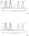
- Figure 11 illustrates an exemplary fabrication process of a FinFET consistent with the disclosed embodiments; and Figures 1-10 illustrate semiconductor structures corresponding to certain stages of the exemplary fabrication process.
- FIG. 11 a substrate with certain structures is provided (S101).
- Figure 1 illustrates a corresponding semiconductor structure.
- a substrate 101 is provided.
- the substrate 101 may include a first region I and a second region II.
- a plurality of first fins 111 may be formed on the surface of the substrate 101 in the first region I; and a plurality of second fins 112 may be formed on the surface of the substrate 101 in the second region II.
- the plurality of first fins 111 and the plurality of second fins 112 may be subsequently processed to cause the plurality of first fins 111 and the plurality of second fins 112 to have different critical dimensions (CDs).
- CDs critical dimensions
- the first region 1 is adjacent to the second region II. In certain other embodiments, the first region I and the second region II may be separated by other regions, or structures, etc.
- the number of the first fins 111 may be any appropriate value, such as 1,2, or 5, etc.
- the number of the second fins 112 may be any appropriate value, such as 1, 2, or 5, etc. In one embodiment, for illustrative purposes, the number of the first fins 111 is 2; and the number of the second fins 112 is 2.
- the substrate 101 may be made of any appropriate semiconductor material, such as silicon, polysilicon, silicon on insulator (SOI), germanium on insulator (GOI), silicon germanium, carborundum, indium antimonite, lead telluride, indium arsenide, indium phosphide, gallium arsenide, gallium antimonite, alloy semiconductor, or a combination thereof.
- the substrate 101 is made of silicon.
- the semiconductor substrate 101 provides a base for subsequent structures and processes.
- the first fins 111 may be made of any appropriate material, such as silicon, germanium, silicon germanium, gallium arsenide, or gallium indium, etc.
- the second fins 112 may be made of any appropriate material, such as silicon, germanium, silicon germanium, gallium arsenide, or gallium indium, etc.
- the first fins 111 are made of silicon; and the second fins 112 is made of silicon.
- the CD of the first fins 111 may be identical to the CD of the second fins 112.
- the process for forming the substrate 101, the first fins 111 and the second fins 112 may include providing an initial substrate; forming a hard mask layer 102 on the initial substrate; and etching the initial substrate using the hard mask layer 102 as an etching mask.
- the initial substrate after the etching process may be referred to as the substrate 101.
- the hard mask layer 102 may be made of any appropriate material, such as one or more of silicon oxide, silicon nitride, silicon oxynitride, and amorphous carbon, etc.
- the hard mask layer 102 may be a single layer structure or a multiple-layer structure. In one embodiment, the hard mask layer 102 is a single layer structure made of silicon nitride.
- the process for forming the hard mask layer 102 may include forming an initial hard mask film; forming a patterned photoresist layer on the initial hard mask film; and etching the initial hard mask film using the patterned photoresist layer as an etching mask.
- the hard mask layer 102 may be formed by a self-aligned double patterning (SADP) method, a self-aligned triple patterning method, or a self-aligned double double patterning method, etc.
- SADP method may include a litho-etch-litho-etch (LELE) method and or a litho-litho-etch (LLE) method.
- the hard mask layer 102 on the top surfaces of the first fins 111 and the second fins 112 may be kept.
- the hard mask layer 102 may protect the top surfaces of the first fins 111 and the second fins 112; and prevent the top surfaces of the first fins 111 and the second fins 112 from being oxidized.
- the top surface of the mask layer 102 may be used as a stop layer; and to protect the tops of the first fins 111 and the second fins 112.
- the size of the top of the fins 11 is smaller than the size of the bottom of the fins 111; and the size of the top of the second fins 112 is smaller than the size of the bottom of the second fins 112.
- the sidewalls of the first fins 111 may be perpendicular to the surface of the substrate 101. That is, the top size of the first fins 111 may be identical to the bottom size of the first fins 111. Further, the sidewall of the second fins 112 may be perpendicular to the surface of the substrate 101. That is, the top size of the second fins 112 may be identical to the bottom size of the second fins 112.
- a liner oxide layer may be formed (S102).
- Figure 2 illustrates a corresponding semiconductor structure.
- a liner oxide layer 103 is formed on the surface of the substrate 101, the side surfaces of the first fins 111 and the side surfaces of the second fins 112.
- the liner oxide layer 103 may be formed by any appropriate process.
- the liner oxide layer 103 is formed by oxidizing the surface of the substrate 101, the side surfaces of the first fins 111 and the side surfaces of the second fins 112.
- the top surfaces of the first fins 111 and the top surfaces of the second fins 112 may be covered by the mask layer 102, the top surfaces of the first fins 111 and the top surfaces of the second fins 112 may not be oxidized. Thus, the height of the first fins 111 and the heights of the second fins 112 may not be changed after the oxidation process.
- the surfaces the protruding corners of the first fins 111 and the second fins 112 may have defects.
- the first fins 111 and the second fins 112 may be oxidized to form the liner oxide layer 103.
- the surface-to-volume ratio of the protruding corners of the first fins 111 and the second fins 112 may be relatively large, it may be easier to oxidize the protruding corners of the first fins 111 and the second fins 112 than other regions.
- the defects on the surfaces of the first fins 111 and the second fins 112 may be removed; and the protruding corners may also be removed. Accordingly, the surfaces of the first fins 111 and the surfaces of the second fins 112 may be relatively smooth, and the quality of the crystal lattices of the first fins 111 and the second fins 112 may be improved. Therefore, the tip-discharging on the first fins 111 and the second fins 112 may be avoided.
- the liner oxide layer 103 may be able to improve the interface properties between subsequently formed insulation layer and the first fins 111 and between the insulation layer and the second fins 112. Thus, the interfacial defects between the insulation layer and the first fins 111 and between the insulation layer and the second fins 112 may be avoided.
- the oxidation process may include any appropriate process, such as an oxygen plasma oxidation process, or a solution of sulphuric acid and hydrogen peroxide oxidation process, etc.
- an in-situ steam generation (1SSG) oxidation process is used to oxidize the substrate 101, the first fins 111 and the second fins 112 to form the liner oxide layer 103. Because the substrate 101, the first fins 111 and the second fins 112 may all be made of silicon, the corresponding liner oxide layer 103 may be made of silicon oxide.
- the liner oxide layer 103 is made of silicon oxide.
- the thickness of the liner oxide layer 103 may be in a range of approximately 5 ⁇ -30 ⁇ .
- an insulating barrier film maybe formed (S103).
- Figure 3 illustrates a corresponding semiconductor structure.
- an insulating barrier film 104 is formed on the surface of the liner oxide layer 103.
- a subsequent etching process may remove the portion of the insulating barrier film 104 on the surface of the liner oxide layer 103 in the second region II.
- the remaining portion of the insulating barrier film 104 on the liner oxide layer 103 in the first region I may be used to reduce the oxidation rate of the sidewalls of the first fins 111 during a subsequent curing annealing process.
- the portion of the insulating barrier film 104 on the liner oxide layer 103 in the second region II may be subsequently removed by an etching process; and the etching process should not etch the liner oxide layer 103 in the second region II, it may require the insulating barrier film 104 and the liner oxide layer 103 to be made of different materials. Further, the insulating barrier film 104 may be made of a material that is easy to be subsequently removed. At the same time, the insulating barrier film 104 may also be an insulation material. The portion of the insulation film 104 in the first region I may be a portion of the insulation layer of the FinFET; and may function as an electrical insulator.
- the insulating barrier film 104 may be made of silicon nitride, silicon oxynitride, silicon carbide, silicon carbonitride, silicon oxycarbonitride, or boron nitride, etc.
- the insulating barrier film 104 is made of silicon nitride. Silicon nitride may have a relatively high compactness.
- the insulating barrier film 104 may be able to prevent the diffusion of H 2 O during the subsequent curing annealing process; and may be able to effectively reduce the quantity of H 2 O contacting with the first fins 111.
- the oxidation scale of the sidewalls of the first fins 111 may be reduced.
- the insulating barrier film 104 is substantially thin, the corresponding subsequently formed insulating barrier layer may also be substantially thin, and the ability for preventing the diffusion of H 2 O may be limited. If the insulating barrier film 104 is significantly thick, it may take a relatively long time to subsequently remove the portion of the insulating film 104 in the second region II. Further, the insulating barrier layer subsequently formed in the first region I may also be significantly thick. Thus, it may reduce the process window of the subsequently formed precursor material layer; and it may be difficult to form a precursor layer having few voids in the first region I. Thus, the thickness of the insulating barrier film 104 may be in a range of the approximately 30 ⁇ -50 ⁇ . In one embodiment, the thickness of the insulating barrier film 104 is approximately 40 ⁇ .
- the insulating barrier film 104 is formed by an ALD process.
- the ALD process may have a relatively high step-coverage ability.
- the insulating barrier film 104 formed by the ALD process may have a desired uniformity. Accordingly, the diffusion barrier ability of the insulating barrier film 104 at different positions of the insulating barrier film 104 may be identical; and the subsequently oxidized sidewalls of the first fins 111 may still have a desired morphology.
- a patterned layer may be formed (S104).
- Figure 4 illustrates a corresponding semiconductor structure.
- a patterned layer 105 is formed on the surface of the portion of the insulating barrier film 104 in the first region I.
- the patterned layer 105 may expose the surface of the portion of the insulating barrier film 104 in the second region II.
- the patterned layer 105 may be used as an mask for subsequently removing the portion of the insulating film 104 the second region II.
- the patterned layer 105 may be made of any appropriate material.
- the pattered layer 105 is a patterned photoresist layer.
- the process for forming the patterned photoresist layer 105 may include forming a photoresist layer on the insulating barrier film 104; and exposing the photoresist layer.
- the top surface of the photoresist layer is higher than the top surface of the hard mask layer 102.
- the exposed photoresist layer may be developed; and the portion of the photoresist layer on the surface of the insulating barrier film 104 in the second region II may be removed.
- the patterned layer 105 may also include a bottom antireflective layer; and a photoresist layer formed on the bottom antireflective layer.
- the patterned layer 105 may also be a hard mask layer.
- the hard mask layer may be made of a material different from those of the insulating barrier film 104 and the liner oxide layer 103.
- an insulating barrier layer may be formed (S105).
- Figure 5 illustrates a corresponding semiconductor structure.
- an insulating barrier layer 106 is formed on the portion of the liner oxide layer 103 in the first region I.
- the insulating barrier layer 106 may be formed by removing the insulating barrier film 104 (referring to Figure 4 ) in the second region II by an etching process using the patterned layer 105 as an etching mask.
- the insulating barrier film 104 may be etched by any appropriate process, such as a dry etching process, or a wet etching process, etc. In one embodiment, a dry etching process is used to etch the insulating barrier film 104. Because the insulating barrier film 104 and the liner oxide layer 103 may be made of different materials, during the dry etching process, the etch rate of the insulating barrier film 104 may be greater than the etching rate of the liner oxide layer 103.
- the insulating barrier layer 106 may be a material identical to that of the insulating barrier film 104. That is, the insulating barrier layer 106 may be made of silicon nitride, silicon oxynitride, silicon carbide, silicon carbonitride, silicon oxycarbonitride, or boron nitride, etc. In one embodiment, the insulating barrier layer 106 is made of silicon nitride. Because silicon nitride may has a relatively high compactness, it may prevent the diffusion of H 2 O during the subsequent curing annealing process; and may be able to effectively reduce the quantity of H 2 O contacting with the side walls of the first fins 111. Accordingly the oxidation rate of the sidewalls of the first fins 111 may be reduced.
- the ability for preventing the diffusion of H 2 O may be limited.
- the quantity of H 2 O contacting with the first fins 111 may be relatively large; and the oxidiation scale of the sidewalls of the first fins 111 may be relatively large.
- the feature size differences between the first fins 111 and the second fins 112 may be relatively small.
- the insulating barrier layer 106 is significantly thick, the process window for subsequently forming a precursor material layer may be relatively small; and voids may be formed in the precursor material layer in the first region I.
- the thickness of the insulating barrier layer 106 may be in a range of the approximately 30 ⁇ -50 ⁇ .
- the thickness of the insulating barrier layer 106 is approximately 40 ⁇ . Such a thickness range may enable the insulating barrier layer 106 to have a relatively strong ability to prevent the diffusion of H 2 O. Further, it may ensure the precursor material subsequently formed in the first region I to have a relatively high gap filling ability.
- the patterned layer 105 may be removed (S106).
- Figure 6 illustrates a corresponding semiconductor structure.
- the patterned layer 105 is removed.
- the patterned layer 105 is made of photoresist, a plasma ashing process, or a wet etching process may be used to remove the patterned layer 105.
- the patterned layer 105 may be a hard mask layer, a dry etching process, or a wet etching process may be used to remove the patterned layer 105.
- a precursor material layer may be formed (S107).
- Figure 7 illustrates a corresponding semiconductor structure.
- a precursor material layer 107 is formed on the surface of the insulating barrier layer 106 in the first region I and the surface of the liner oxide layer 103 in the second region II.
- the precursor material layer 107 may be flowable.
- the top of the precursor material layer 107 may be higher than the tops of the first fins 111 and the tops of the second fins 112.
- the precursor material layer 107 may be used to subsequently form an insulation layer among the first fins 111 and the second fins 112.
- the flowable material may be used to form the precursor material layer 107 on the surface of the insulating barrier layer 106 in the first region I and the surface of the liner oxide layer 103 in the second region II. Because the precursor material layer 107 may be flowable with a certain degree of the viscosity. Thus, a void-less filling may be achieved between adjacent first fins 111, between adjacent second fins 112 and between the first fins 111 and the adjacent second fins 112.
- the precursor material layer 107 is formed by a flowable-CVD (FCVD) process.
- FCVD flowable-CVD
- the substrate 101 may be kept at a pre-determined temperature range, the reaction precursors of the FCVD process may be able to flow into the gaps among the first fins 111, the gaps among the second fins 112 and the gaps among the first fins 111 and the second fins 112.
- the flowable precursor material layer 107 may be formed; and the top of the precursor material layer 107 may be higher than the hard mask layer 102.
- the reaction precursor of the FCVD process may include one or more of saline, disaline, methylsaline, dimethylsaline, trimethylsaline, tetramethylsaline, tetraethyl orthosilicate, (3-Aminopropyl) triethoxysilane, octamethyl cyclotetrasiloxane, 1,1,3,3-tetramethyldisiloxane, tetramethylcyclotetrasiloxane, trisilylamine, and disilylamine, etc.
- the reaction precursors may also be other silylamine and their derivatives, etc.
- trimethylsaline is used as the reaction precursor of the FCVD process to form the precursor material layer 107.
- the FCVD process may be performed in a NH 3 environment.
- the substrate 101 with the formed structures may be placed in a reaction chamber; and the reaction precursor and NH 3 may be introduced into the reaction chamber to perform the FCVD process.
- the flow rate of the reaction precursor may be in a range of approximately 100 sccm-3000 sccm.
- the flow rate of NH 3 may be in a range of approximately 20 sccm-1000 sccm.
- the pressure of the reaction chamber may be in a range of approximately 0.1 Torr-10 Torr.
- the temperature of the reaction chamber may be in a range of approximately 20°C-150°C.
- Inert gas, such as Ar, He, or, Xe, etc. may be also be introduced into the reaction chamber.
- the flow rate of the inert gas may be in a range of approximately 1000 sccm-10000 sccm.
- the reaction precursor of the FCVD process may include Si element. Further, the FCVD process may be performed in an N-containing environment. Thus, the precursor material layer 107 may include at least N atoms and Si atoms. Further, the precursor material layer 107 may also include H atoms. Specifically, the formed precursor material layer 107 may have Si-H bonds, Si-N bonds and Si-N-H bonds, etc. During the subsequent curing annealing process, N atoms in such chemical bonds may be substituted by O atoms; and O-Si-O, and Si-O bonds, etc., may be formed. Thus, an insulation layer made of SiO 2 may be formed.
- an insulation layer may be formed (S108).
- Figure 8 illustrates a corresponding semiconductor structure.
- an insulation layer 108 is formed.
- the insulation layer 108 may be formed by converting the precursor material layer 107 using a curing annealing process (not labeled).
- the curing annealing process may be performed in an H 2 O-containing environment.
- the chemical bonds in the precursor material layer 107 may be broken, and/or rearranged, to form new chemical bonds and/or function groups.
- the O ions in H 2 O may diffuse into the precursor material layer 107, and the broken Si bonds, N bonds and H bonds may combine with the O ions to form new chemical bonds, such as Si-O-H bonds, Si-O bonds and O-Si-O bonds, etc.
- the precursor material layer 107 may be converted into the insulation layer 108; and the insulation layer 108 may be made of silicon oxide.
- the top of the insulation layer 108 may be higher than the top of the mask layer 102.
- the environment of the curing annealing process may also include one or more of O 2 gas and O 3 gas, etc.
- the temperature of the curing annealing process may be in a range of approximately 400°C-500°C.
- H 2 O may diffuse into the precursor material layer 107.
- H 2 O may diffuse into the side surfaces of the first fins 111 through the liner oxide layer 103 and the insulating barrier layer 106 to form a first oxide layer (not shown).
- H 2 O may diffuse into the side surfaces of the second fins 112 through the liner oxide layer 103; and the side surfaces of the second fins 112 may be oxidized to form a second oxide layer 122.
- the oxidation scale of the side surfaces of the first fins 111 may be lower than the oxidation scale of the side surfaces of the second fins 122.
- the thickness of the first oxide layer may be smaller than the thickness of the second oxide layer 122.
- the feature size of the first fins 111 may be identical to the feature size of the second fins 112 before forming the first oxide layer and the second oxide layer 122, after forming the first oxide layer and the second oxide layer 122, the feature size of the first fins 111 may be greater than the feature size of the second fins 122.
- the thickness of the first oxide layer may be approximately 0; and the thickness of the second oxide layer 122 may be in a range of approximately 3 nm-5 nm. In certain other embodiments, the thickness of the first oxide layer may be greater than 0.
- the thickness difference between the first oxide layer and the second oxide layer 122 may be in a range of approximately 3 nm-5 nm. That is, after forming the first oxide layer and the second oxide layer 122, the feature size difference between the first fins 111 and the second fins 122 may be in a range of approximately 3 nm-5 nm. In certain other embodiments, when the thickness of the insulating barrier layer 106 and/or the parameters of the curing annealing process are changed, the thickness difference between the first oxide layer and the second oxide layer 122 may also be changed.
- a second annealing process may be performed on the precursor material layer 107.
- the second annealing process may be performed in a N 2 environment.
- the temperature of the second annealing process may be in a range of approximately 900°C-1 100°C.
- the annealing temperature may be in a range of approximately 900°C-1000°C.
- FIG. 9 illustrates a corresponding semiconductor structure.
- the portion of the insulation layer 108 higher than the mask layer 102 may be removed by any appropriate process.
- a chemical mechanical polishing process is used to remove the portion of the insulation layer 108 higher than the mask layer 102.
- the chemical mechanical polishing process may be stopped on the top surface of the mask layer 102.
- the mask layer 102 may be used to protect the top surfaces of the first fins 111 and the second fins 112; and the damages caused by the chemical mechanical polishing process may be avoided.
- the hard mask layer 102 may be removed.
- Various processes may be used to remove the hard mask layer 102, such as a dry etching process, or a wet etching process, etc. In one embodiment, a wet etching process is used to remove the hard mask layer 102.
- the hard mask layer 102 is made of silicon nitride.
- the etching solution of the wet etching process may be a phosphoric acid solution.
- the mass percentage of the phosphoric acid may be in a range of approximately 65%-85%.
- the temperature of the etching solution may be in a range of approximately 120°C-200°C.
- an isolation layer may be formed (S 110).
- Figure 10 illustrates a corresponding semiconductor structure.
- a top portion of the insulation layer 108 is removed; and an isolation layer 118 is formed. Further, the portion of the liner oxide layer 103 higher than the top surface of the insolation layer 118, the portion of the insulating barrier layer 106 higher than the top surface of the insolation layer 118, the portion of the first oxide layer (not shown) higher than the top surface of the insolation layer 118 and the portion of the second oxide layer 122 higher than the top surface of the insolation layer 118 may be removed. Thus, the top portions of the side surfaces of the first fins 111 and the top portions of the side surfaces of the second fins 122 may be exposed.
- the top portions of the insulation layer 108, the liner oxide layer 103, the insulating barrier layer 106, the first oxide layer and the second oxide layer 122 may be removed by any appropriate process, such as a dry etching process, a wet etching process and a SiCoNi system etching process, etc.
- the top portions of the insulation layer 108, the liner oxide layer 103, the insulating barrier layer 106, the first oxide layer and the second oxide layer 122 may be removed by a same etching process.
- the top portions of the insulation layer 108, the liner oxide layer 103, the insulating barrier layer 106, the first oxide layer and the second oxide layer 122 may be removed by different processes.
- the top portion of the insulation layer 108 is removed by a wet etching process.
- the etching solution may be a HF solution.
- the portion of the insulating barrier layer 106 higher than the top surface of the isolation layer 118 is removed by a wet etching process.
- the etching solution is a phosphoric acid solution.
- the mass percentage of the phosphoric acid solution may be in a range of approximately 65%-85%.
- the temperature of the etching solution may be in a range of approximately 120°C-200°C.
- the feature size of the first fins 111 higher than the isolation layer 118 may be greater than the feature size of the second fins 122 higher than the isolation layer 118.
- the feature size difference may be in range of approximately 3 nm-5 nm.
- the mask layer 102 may be removed before forming the isolation layer 118 and after forming the insulation layer 108. In certain other embodiments, the mask layer 102 may be removed after forming the isolation layer 118.
- a first gate structure crossing over the first fins 111 may be formed on the surface of the isolation layer 118 in the first region I.
- the first gate structure may cover the top and side surfaces of the first fins 111.
- first source/drain regions may be formed in the first fins 111 at the two sides of the first gate structure.
- a second gate structure crossing over the second fins 122 may be formed on the surface of the isolation layer 118 in the second region II.
- the second gate structure may cover the top and side surfaces of the second fins 122.
- second source/drain regions may be formed in the first second fins 122 at the two sides of the second gate structure.
- a FinFET structure may be formed by the disclosed methods and processes.
- the corresponding FinFET structure is illustrated in Figures 10 .
- the FinFET structure may include a substrate 101 having a first region I and a second region II.
- the FinFET structure may also include a plurality of first fins 111 formed on the substrate 101 in the first region I and a plurality of second fins 112 with a feature size different from a feature size of the first fins 111 formed on the substrate 101 in the second region II.
- the FinFET structure may also include a liner oxide layer 103 formed on the surface of the substrate 101 and the portions of the side surfaces of the first fins 111 and the second fins 122; and an insulating layer 106 formed on the liner oxide layer 103 in the first region I.
- the FinFET structure may also include a second oxide layer 122 formed between the side surfaces of the second fins 112 and the liner oxide layer 103 in the second region II; and an isolation layer 118 with a top surface lower than the top surfaces of the first fins 111 and the second fins 112 formed on the insulating barrier layer 106 in the first region I and on the liner oxide layer 103 in the second region II.
- the detailed structures and intermediate structures are described above with respect to the fabrication processes.
- the oxidation scale of the side surfaces of the first fins may be reduced during the subsequent curing annealing process.
- the feature size of the first fins may be greater than the feature size of the first fins. That is, fins with different sizes may be formed by the disclosed method.
- a curing annealing process may be performed on the precursor material layer, by using the oxidation scale difference between the first fins and the second fins during the curing annealing process of the precursor material layer, fins with different feature sizes may be obtained.
- the existing required methods forming fins may be effectively used; and the process for forming the FinFET may be simplified; and the process difficulties for forming the FinFET having fins with different sizes may be reduced. Further, comparing with the method for forming fins with a same size, only one mask may be added to form the fins with different sizes.
Landscapes
- Formation Of Insulating Films (AREA)
- Thin Film Transistor (AREA)
- Chemical & Material Sciences (AREA)
- Chemical Kinetics & Catalysis (AREA)
- General Chemical & Material Sciences (AREA)
- Element Separation (AREA)
Abstract
Description
- This application claims the priority of Chinese patent application No.
201610008863.2, filed on January 7, 2016 - The present invention generally relates to the field of semiconductor manufacturing technology and, more particularly, relates to fin field-effect transistors (FinFETs) and fabrication processes thereof.
- With the rapid development of semiconductor manufacturing technology, the technical node of the semiconductor technology has been continuously shrunk by following the Moore's Law. To adapt to the reduced technical node, the channel length of the MOSFETs has to be continually reduced. Reducing the channel length of the MOSFETs is able to increase the device density of the integrate circuits (ICs); and increase the switching speed of the MOSFETs, etc.
- However, with the continuously shrinking the channel length, the distance between the source and the drain of the device has also be correspondingly reduced. Accordingly, the control ability of the gate on the channel region is reduced; and the difficulty for the gate voltage to pinch off the channel region is increased. Thus, the subthreshold leakage phenomenon may occur. That is, it may be easier to have the short channel effects (SCEs).
- Thus, to meet the miniaturization requirements of the semiconductor devices, the semiconductor technology has been gradually developed from the planar MOSFETs to the three-dimensional transistors that have better performances. Fin field-effect transistors (FinFETs) are a typical type of three-dimensional devices.
- In a FinFET, the gate is able to control the ultrathin components (i.e., fins) from at least two sides. Thus, comparing with a planar MOSFET, the gate of the FinFET has a stronger control ability on the channel region; and may be able to effectively inhibit the SCEs. Further, comparing with other devices, FinFETs have better compatibilities with the existing IC manufacturing technologies.
- However, in the existing technologies, when fins with different critical dimensions (CDs) need to be formed in the FinFET, the fabrication processes may be relatively complex. The disclosed device structures and methods are directed to solve one or more problems set forth above and other problems in the art.
- A first aspect of the present invention includes a method for fabricating a fin field-effect transistor (FinFET). The method includes providing a substrate having a first region and a second region; forming a plurality of first fins on the substrate in the first region and a plurality of second fins on the substrate in the second region; forming a liner oxide layer on side surfaces of the first fins, side surfaces of the second fins and a surface of the substrate; forming an insulating barrier layer on a portion of the liner oxide layer in the first region; forming a precursor material layer on the insulating barrier layer in the first region and on the liner oxide layer in the second region; performing a curing annealing process to convert the precursor material into an insulation layer, a first oxide layer being formed on the side surfaces of the first fins, and a second oxide layer being formed on the side surfaces of the second fins; and removing a top portion of the insulation layer to form an isolating layer and removing portions of the liner oxide layer, the insulating barrier layer, the first oxide layer and the second oxide layer higher than a surface of the isolating layer.
- Preferably, a feature size of the first fins is identical to a feature size of the second fins before forming the liner oxide layer.
- Preferably, a feature size of portions of the first fins higher than the surface of the isolation layer is greater than a feature size of portions of the second fins higher than the surface of the isolation layer after removing portions of the liner oxide layer, the insulation layer, the first oxide layer and the second oxide layer higher the surface of the isolation layer.
- Forming the insulating barrier layer may comprise: forming an insulating barrier film on the liner oxide layer; forming a patterned layer on the liner oxide layer in the first region; and removing a portion of the insulating barrier film in the second region by etching the insulating barrier film using the patterned layer as an etching mask.
- Preferably, a thickness difference between the first oxide layer and the second oxide layer is in a range of approximately 3 nm-5 nm.
- Preferably, a feature size difference between the portions of the first fins higher than the isolation layer and the portions of the second fins higher than the isolation layer is in a range of approximately 3 mn-5 nm.
- Preferably, the precursor material layer is flowable. Most preferably, the precursor material layer is formed by a flowable chemical vapor deposition process.
- For example, precursors of the flowable chemical vapor deposition process may include one or more of saline, disaline, methylsaline, dimethylsaline, trimethylsaline, tetramethylsaline, tetraethyl orthosilicate, (3-Aminopropyl) triethoxysilane, octamethyl cyclotetrasiloxane, 1,1,3,3-tetramethyldisiloxane, tetramethylcyclotetrasiloxane, trisilylamine, and disilylamine.
- Preferably, the curing annealing process is performed in a H2O-containing environment. Most preferably, the H2O-containing environment may further comprise: one or more of O2 and O3.
- Preferably, a temperature of the curing annealing process is in a range of approximately 400°C-500°C.
- After the curing annealing process, the method may further comprise: performing a second annealing process to the precursor material layer, wherein: a temperature of the second annealing process is in a range of approximately 900°C-1100°C; and the second annealing process is performed in a N2 environment.
- Preferably, the top portion of the insulation layer is removed by a wet etching process to form the isolation layer.
- Preferably, the liner oxide layer is formed by an in situ steam generation oxidation process.
- Before forming the liner oxide layer, the method may further comprise: forming a hard mask layer on top surfaces of the first fins and top surfaces of the second fins, wherein: the insulating barrier layer covers the hard mask layer in the first region; and a top of the insulating barrier layer is higher than a top of the hard mask layer.
- Before removing the top portion of the insulation layer, the method may further comprise: polishing the insulation layer until a top surface of the hard mask layer is exposed.
- Preferably, the hard mask layer is removed.
- A second aspect of the present invention includes a fin field-effect transistor (FinFET). The fin field-effect transistor includes a substrate having a first region and a second region; a plurality of first fins formed on the substrate in the first region and a plurality of second fins with a feature size different from a feature size of the first fins formed on the substrate in the second region; a liner oxide layer formed on the surface of the substrate and bottom portions of side surfaces of the first fins and the second fins; an insulating barrier layer formed on the liner oxide layer in the first region; a first oxide layer formed between the bottom side surfaces of the first fins and the liner oxide layer in the first region and a second oxide layer with a thickness different from a thickness of the first oxide layer formed between the bottom side surfaces of the second fins and the liner oxide layer in the second region; and an isolation layer with a top surface lower than the top surfaces of the first fins and the second fins formed on insulating barrier layer in the first region and on the liner oxide layer in the second region.
- Preferably, a feature size difference between the first fins and the second fins is in range of approximately 3 nm-5 nm.
- Preferably, a thickness difference between the first oxide layer and the second oxide layer is in a range of approximately 3 nm-5 nm.
- Preferably, the insulating barrier layer is made of one of silicon nitride, silicon oxynitride, silicon carbide, silicon carbonitride, silicon oxycarbonitride, and boron nitride.
- Preferably, a thickness of the insulating barrier layer is in a range of approximately 30Å-50Å.
- Preferably, the liner oxide layer is made of one of silicon oxide and silicon oxynitride.
- Other aspects of the present invention can be understood by those skilled in the art in light of the description, the claims, and the drawings of the present invention.
-
-
Figures 1-10 illustrate semiconductor structures corresponding to certain stages of an exemplary fabrication process of a FinFET consistent with the disclosed embodiments; and -
Figure 11 illustrates an exemplary fabrication process of a FinFET consistent with the disclosed embodiments. - Reference will now be made in detail to exemplary embodiments of the invention, which are illustrated in the accompanying drawings. Wherever possible, the same reference numbers will be used throughout the drawings to refer to the same or like parts.
-
Figure 11 illustrates an exemplary fabrication process of a FinFET consistent with the disclosed embodiments; andFigures 1-10 illustrate semiconductor structures corresponding to certain stages of the exemplary fabrication process. - As shown in
Figure 11 , at the beginning of fabrication process, a substrate with certain structures is provided (S101).Figure 1 illustrates a corresponding semiconductor structure. - As shown in
Figure 1 , asubstrate 101 is provided. Thesubstrate 101 may include a first region I and a second region II. A plurality offirst fins 111 may be formed on the surface of thesubstrate 101 in the first region I; and a plurality ofsecond fins 112 may be formed on the surface of thesubstrate 101 in the second region II. The plurality offirst fins 111 and the plurality ofsecond fins 112 may be subsequently processed to cause the plurality offirst fins 111 and the plurality ofsecond fins 112 to have different critical dimensions (CDs). - In one embodiment, the first region 1 is adjacent to the second region II. In certain other embodiments, the first region I and the second region II may be separated by other regions, or structures, etc.
- The number of the
first fins 111 may be any appropriate value, such as 1,2, or 5, etc. The number of thesecond fins 112 may be any appropriate value, such as 1, 2, or 5, etc. In one embodiment, for illustrative purposes, the number of thefirst fins 111 is 2; and the number of thesecond fins 112 is 2. - The
substrate 101 may be made of any appropriate semiconductor material, such as silicon, polysilicon, silicon on insulator (SOI), germanium on insulator (GOI), silicon germanium, carborundum, indium antimonite, lead telluride, indium arsenide, indium phosphide, gallium arsenide, gallium antimonite, alloy semiconductor, or a combination thereof. In one embodiment, thesubstrate 101 is made of silicon. Thesemiconductor substrate 101 provides a base for subsequent structures and processes. - The
first fins 111 may be made of any appropriate material, such as silicon, germanium, silicon germanium, gallium arsenide, or gallium indium, etc. Thesecond fins 112 may be made of any appropriate material, such as silicon, germanium, silicon germanium, gallium arsenide, or gallium indium, etc. In one embodiment, thefirst fins 111 are made of silicon; and thesecond fins 112 is made of silicon. - The CD of the
first fins 111 may be identical to the CD of thesecond fins 112. The process for forming thesubstrate 101, thefirst fins 111 and thesecond fins 112 may include providing an initial substrate; forming ahard mask layer 102 on the initial substrate; and etching the initial substrate using thehard mask layer 102 as an etching mask. The initial substrate after the etching process may be referred to as thesubstrate 101. The protruding parts on the surface of thesubstrate 101 in the first region I may be referred to as thefirst fins 111; and the protruding parts on the surface of thesubstrate 101 in the second region II may be referred to as thesecond fins 112. - The
hard mask layer 102 may be made of any appropriate material, such as one or more of silicon oxide, silicon nitride, silicon oxynitride, and amorphous carbon, etc. Thehard mask layer 102 may be a single layer structure or a multiple-layer structure. In one embodiment, thehard mask layer 102 is a single layer structure made of silicon nitride. - The process for forming the
hard mask layer 102 may include forming an initial hard mask film; forming a patterned photoresist layer on the initial hard mask film; and etching the initial hard mask film using the patterned photoresist layer as an etching mask. In certain other embodiments, thehard mask layer 102 may be formed by a self-aligned double patterning (SADP) method, a self-aligned triple patterning method, or a self-aligned double double patterning method, etc. The SADP method may include a litho-etch-litho-etch (LELE) method and or a litho-litho-etch (LLE) method. - In one embodiment, after forming the
first fins 111 and thesecond fins 112, thehard mask layer 102 on the top surfaces of thefirst fins 111 and thesecond fins 112 may be kept. Thehard mask layer 102 may protect the top surfaces of thefirst fins 111 and thesecond fins 112; and prevent the top surfaces of thefirst fins 111 and thesecond fins 112 from being oxidized. Further during the subsequent planarization process, the top surface of themask layer 102 may be used as a stop layer; and to protect the tops of thefirst fins 111 and thesecond fins 112. - In one embodiment, as shown in
Figure 1 , the size of the top of the fins 11 is smaller than the size of the bottom of thefins 111; and the size of the top of thesecond fins 112 is smaller than the size of the bottom of thesecond fins 112. In certain other embodiments, the sidewalls of thefirst fins 111 may be perpendicular to the surface of thesubstrate 101. That is, the top size of thefirst fins 111 may be identical to the bottom size of thefirst fins 111. Further, the sidewall of thesecond fins 112 may be perpendicular to the surface of thesubstrate 101. That is, the top size of thesecond fins 112 may be identical to the bottom size of thesecond fins 112. - Returning to
Figure 11 , after forming thefirst fins 111 and thesecond fins 112, a liner oxide layer may be formed (S102).Figure 2 illustrates a corresponding semiconductor structure. - As shown in
Figure 2 , aliner oxide layer 103 is formed on the surface of thesubstrate 101, the side surfaces of thefirst fins 111 and the side surfaces of thesecond fins 112. Theliner oxide layer 103 may be formed by any appropriate process. In one embodiment, theliner oxide layer 103 is formed by oxidizing the surface of thesubstrate 101, the side surfaces of thefirst fins 111 and the side surfaces of thesecond fins 112. - Because the top surfaces of the
first fins 111 and the top surfaces of thesecond fins 112 may be covered by themask layer 102, the top surfaces of thefirst fins 111 and the top surfaces of thesecond fins 112 may not be oxidized. Thus, the height of thefirst fins 111 and the heights of thesecond fins 112 may not be changed after the oxidation process. - Because the
first fins 111 and thesecond fins 112 may be formed by etching the initial substrate, the surfaces the protruding corners of thefirst fins 111 and thesecond fins 112 may have defects. In one embodiment, thefirst fins 111 and thesecond fins 112 may be oxidized to form theliner oxide layer 103. During the oxidation process, because the surface-to-volume ratio of the protruding corners of thefirst fins 111 and thesecond fins 112 may be relatively large, it may be easier to oxidize the protruding corners of thefirst fins 111 and thesecond fins 112 than other regions. Thus, after subsequently removing theliner oxide layer 103, the defects on the surfaces of thefirst fins 111 and thesecond fins 112 may be removed; and the protruding corners may also be removed. Accordingly, the surfaces of thefirst fins 111 and the surfaces of thesecond fins 112 may be relatively smooth, and the quality of the crystal lattices of thefirst fins 111 and thesecond fins 112 may be improved. Therefore, the tip-discharging on thefirst fins 111 and thesecond fins 112 may be avoided. - Further, the
liner oxide layer 103 may be able to improve the interface properties between subsequently formed insulation layer and thefirst fins 111 and between the insulation layer and thesecond fins 112. Thus, the interfacial defects between the insulation layer and thefirst fins 111 and between the insulation layer and thesecond fins 112 may be avoided. - The oxidation process may include any appropriate process, such as an oxygen plasma oxidation process, or a solution of sulphuric acid and hydrogen peroxide oxidation process, etc. In one embodiment, an in-situ steam generation (1SSG) oxidation process is used to oxidize the
substrate 101, thefirst fins 111 and thesecond fins 112 to form theliner oxide layer 103. Because thesubstrate 101, thefirst fins 111 and thesecond fins 112 may all be made of silicon, the correspondingliner oxide layer 103 may be made of silicon oxide. - In one embodiment, the
liner oxide layer 103 is made of silicon oxide. The thickness of theliner oxide layer 103 may be in a range of approximately 5Å-30Å. - Returning to
Figure 11 , after forming theliner oxide layer 103, an insulating barrier film maybe formed (S103).Figure 3 illustrates a corresponding semiconductor structure. - As shown in
Figure 3 , an insulatingbarrier film 104 is formed on the surface of theliner oxide layer 103. A subsequent etching process may remove the portion of the insulatingbarrier film 104 on the surface of theliner oxide layer 103 in the second region II. The remaining portion of the insulatingbarrier film 104 on theliner oxide layer 103 in the first region I may be used to reduce the oxidation rate of the sidewalls of thefirst fins 111 during a subsequent curing annealing process. - Because the portion of the insulating
barrier film 104 on theliner oxide layer 103 in the second region II may be subsequently removed by an etching process; and the etching process should not etch theliner oxide layer 103 in the second region II, it may require the insulatingbarrier film 104 and theliner oxide layer 103 to be made of different materials. Further, the insulatingbarrier film 104 may be made of a material that is easy to be subsequently removed. At the same time, the insulatingbarrier film 104 may also be an insulation material. The portion of theinsulation film 104 in the first region I may be a portion of the insulation layer of the FinFET; and may function as an electrical insulator. - Thus, the insulating
barrier film 104 may be made of silicon nitride, silicon oxynitride, silicon carbide, silicon carbonitride, silicon oxycarbonitride, or boron nitride, etc. In one embodiment, the insulatingbarrier film 104 is made of silicon nitride. Silicon nitride may have a relatively high compactness. Thus, the insulatingbarrier film 104 may be able to prevent the diffusion of H2O during the subsequent curing annealing process; and may be able to effectively reduce the quantity of H2O contacting with thefirst fins 111. Thus, the oxidation scale of the sidewalls of thefirst fins 111 may be reduced. - If the insulating
barrier film 104 is substantially thin, the corresponding subsequently formed insulating barrier layer may also be substantially thin, and the ability for preventing the diffusion of H2O may be limited. If the insulatingbarrier film 104 is significantly thick, it may take a relatively long time to subsequently remove the portion of the insulatingfilm 104 in the second region II. Further, the insulating barrier layer subsequently formed in the first region I may also be significantly thick. Thus, it may reduce the process window of the subsequently formed precursor material layer; and it may be difficult to form a precursor layer having few voids in the first region I. Thus, the thickness of the insulatingbarrier film 104 may be in a range of the approximately 30Å-50Å. In one embodiment, the thickness of the insulatingbarrier film 104 is approximately 40Å. - Various processes may be used to form the insulating
barrier film 104, such as a chemical vapor deposition (CVD) process, a physical vapor deposition (PVD) process, or an atomic layer deposition (ALD) process, etc. In one embodiment, the insulatingbarrier film 104 is formed by an ALD process. The ALD process may have a relatively high step-coverage ability. Thus, the insulatingbarrier film 104 formed by the ALD process may have a desired uniformity. Accordingly, the diffusion barrier ability of the insulatingbarrier film 104 at different positions of the insulatingbarrier film 104 may be identical; and the subsequently oxidized sidewalls of thefirst fins 111 may still have a desired morphology. - Returning to
Figure 11 , after forming the insulatingbarrier film 104, a patterned layer may be formed (S104).Figure 4 illustrates a corresponding semiconductor structure. - As shown in
Figure 4 , apatterned layer 105 is formed on the surface of the portion of the insulatingbarrier film 104 in the first region I. The patternedlayer 105 may expose the surface of the portion of the insulatingbarrier film 104 in the second region II. The patternedlayer 105 may be used as an mask for subsequently removing the portion of the insulatingfilm 104 the second region II. - The patterned
layer 105 may be made of any appropriate material. In one embodiment, the patteredlayer 105 is a patterned photoresist layer. The process for forming the patternedphotoresist layer 105 may include forming a photoresist layer on the insulatingbarrier film 104; and exposing the photoresist layer. The top surface of the photoresist layer is higher than the top surface of thehard mask layer 102. After exposing photoresist layer, the exposed photoresist layer may be developed; and the portion of the photoresist layer on the surface of the insulatingbarrier film 104 in the second region II may be removed. - In certain other embodiments, the patterned
layer 105 may also include a bottom antireflective layer; and a photoresist layer formed on the bottom antireflective layer. The patternedlayer 105 may also be a hard mask layer. The hard mask layer may be made of a material different from those of the insulatingbarrier film 104 and theliner oxide layer 103. - Returning to
Figure 11 , after forming the patternedlayer 105, an insulating barrier layer may be formed (S105).Figure 5 illustrates a corresponding semiconductor structure. - As shown in
Figure 5 , an insulatingbarrier layer 106 is formed on the portion of theliner oxide layer 103 in the first region I. The insulatingbarrier layer 106 may be formed by removing the insulating barrier film 104 (referring toFigure 4 ) in the second region II by an etching process using the patternedlayer 105 as an etching mask. - The insulating
barrier film 104 may be etched by any appropriate process, such as a dry etching process, or a wet etching process, etc. In one embodiment, a dry etching process is used to etch the insulatingbarrier film 104. Because the insulatingbarrier film 104 and theliner oxide layer 103 may be made of different materials, during the dry etching process, the etch rate of the insulatingbarrier film 104 may be greater than the etching rate of theliner oxide layer 103. - The insulating
barrier layer 106 may be a material identical to that of the insulatingbarrier film 104. That is, the insulatingbarrier layer 106 may be made of silicon nitride, silicon oxynitride, silicon carbide, silicon carbonitride, silicon oxycarbonitride, or boron nitride, etc. In one embodiment, the insulatingbarrier layer 106 is made of silicon nitride. Because silicon nitride may has a relatively high compactness, it may prevent the diffusion of H2O during the subsequent curing annealing process; and may be able to effectively reduce the quantity of H2O contacting with the side walls of thefirst fins 111. Accordingly the oxidation rate of the sidewalls of thefirst fins 111 may be reduced. - If the insulating
barrier layer 106 is substantially thin, the ability for preventing the diffusion of H2O may be limited. The quantity of H2O contacting with thefirst fins 111 may be relatively large; and the oxidiation scale of the sidewalls of thefirst fins 111 may be relatively large. Thus, during the subsequent curing annealing process, the feature size differences between thefirst fins 111 and thesecond fins 112 may be relatively small. If the insulatingbarrier layer 106 is significantly thick, the process window for subsequently forming a precursor material layer may be relatively small; and voids may be formed in the precursor material layer in the first region I. Thus, the thickness of the insulatingbarrier layer 106 may be in a range of the approximately 30Å-50Å. In one embodiment, the thickness of the insulatingbarrier layer 106 is approximately 40Å. Such a thickness range may enable the insulatingbarrier layer 106 to have a relatively strong ability to prevent the diffusion of H2O. Further, it may ensure the precursor material subsequently formed in the first region I to have a relatively high gap filling ability. - Returning to
Figure 11 , after forming the insulatingbarrier layer 106, the patternedlayer 105 may be removed (S106).Figure 6 illustrates a corresponding semiconductor structure. - As shown in
Figure 6 , the patternedlayer 105 is removed. In one embodiment, the patternedlayer 105 is made of photoresist, a plasma ashing process, or a wet etching process may be used to remove the patternedlayer 105. In certain other embodiments, the patternedlayer 105 may be a hard mask layer, a dry etching process, or a wet etching process may be used to remove the patternedlayer 105. - Returning to
Figure 11 , after removing the patternedlayer 105, a precursor material layer may be formed (S107).Figure 7 illustrates a corresponding semiconductor structure. - As shown in
Figure 7 , aprecursor material layer 107 is formed on the surface of the insulatingbarrier layer 106 in the first region I and the surface of theliner oxide layer 103 in the second region II. Theprecursor material layer 107 may be flowable. The top of theprecursor material layer 107 may be higher than the tops of thefirst fins 111 and the tops of thesecond fins 112. Theprecursor material layer 107 may be used to subsequently form an insulation layer among thefirst fins 111 and thesecond fins 112. - With the continuous shrinking of the size of the semiconductor devices, the distances between adjacent
first fins 111 and the distances between adjacentsecond fins 112 have become smaller and smaller. To improve the gap filling ability of the subsequently formed insulation layer, the flowable material may be used to form theprecursor material layer 107 on the surface of the insulatingbarrier layer 106 in the first region I and the surface of theliner oxide layer 103 in the second region II. Because theprecursor material layer 107 may be flowable with a certain degree of the viscosity. Thus, a void-less filling may be achieved between adjacentfirst fins 111, between adjacentsecond fins 112 and between thefirst fins 111 and the adjacentsecond fins 112. - Various processes may be used to form the
precursor material layer 107. In one embodiment, theprecursor material layer 107 is formed by a flowable-CVD (FCVD) process. During the FCVD process, thesubstrate 101 may be kept at a pre-determined temperature range, the reaction precursors of the FCVD process may be able to flow into the gaps among thefirst fins 111, the gaps among thesecond fins 112 and the gaps among thefirst fins 111 and thesecond fins 112. Thus, the flowableprecursor material layer 107 may be formed; and the top of theprecursor material layer 107 may be higher than thehard mask layer 102. - The reaction precursor of the FCVD process may include one or more of saline, disaline, methylsaline, dimethylsaline, trimethylsaline, tetramethylsaline, tetraethyl orthosilicate, (3-Aminopropyl) triethoxysilane, octamethyl cyclotetrasiloxane, 1,1,3,3-tetramethyldisiloxane, tetramethylcyclotetrasiloxane, trisilylamine, and disilylamine, etc. The reaction precursors may also be other silylamine and their derivatives, etc.
- In one embodiment, trimethylsaline is used as the reaction precursor of the FCVD process to form the
precursor material layer 107. The FCVD process may be performed in a NH3 environment. - Specifically, the
substrate 101 with the formed structures may be placed in a reaction chamber; and the reaction precursor and NH3 may be introduced into the reaction chamber to perform the FCVD process. The flow rate of the reaction precursor may be in a range of approximately 100 sccm-3000 sccm. The flow rate of NH3 may be in a range of approximately 20 sccm-1000 sccm. The pressure of the reaction chamber may be in a range of approximately 0.1 Torr-10 Torr. The temperature of the reaction chamber may be in a range of approximately 20°C-150°C. Inert gas, such as Ar, He, or, Xe, etc., may be also be introduced into the reaction chamber. The flow rate of the inert gas may be in a range of approximately 1000 sccm-10000 sccm. - The reaction precursor of the FCVD process may include Si element. Further, the FCVD process may be performed in an N-containing environment. Thus, the
precursor material layer 107 may include at least N atoms and Si atoms. Further, theprecursor material layer 107 may also include H atoms. Specifically, the formedprecursor material layer 107 may have Si-H bonds, Si-N bonds and Si-N-H bonds, etc. During the subsequent curing annealing process, N atoms in such chemical bonds may be substituted by O atoms; and O-Si-O, and Si-O bonds, etc., may be formed. Thus, an insulation layer made of SiO2 may be formed. - Returning to
Figure 11 , after forming theprecursor material layer 107, an insulation layer may be formed (S108).Figure 8 illustrates a corresponding semiconductor structure. - As shown
Figure 8 , aninsulation layer 108 is formed. Theinsulation layer 108 may be formed by converting theprecursor material layer 107 using a curing annealing process (not labeled). - In one embodiment, the curing annealing process may be performed in an H2O-containing environment. In the H2O-containing environment, the chemical bonds in the
precursor material layer 107 may be broken, and/or rearranged, to form new chemical bonds and/or function groups. The O ions in H2O may diffuse into theprecursor material layer 107, and the broken Si bonds, N bonds and H bonds may combine with the O ions to form new chemical bonds, such as Si-O-H bonds, Si-O bonds and O-Si-O bonds, etc. Thus, theprecursor material layer 107 may be converted into theinsulation layer 108; and theinsulation layer 108 may be made of silicon oxide. The top of theinsulation layer 108 may be higher than the top of themask layer 102. - The environment of the curing annealing process may also include one or more of O2 gas and O3 gas, etc. The temperature of the curing annealing process may be in a range of approximately 400°C-500°C.
- In the H2O-containing environment, H2O may diffuse into the
precursor material layer 107. In the first region I, H2O may diffuse into the side surfaces of thefirst fins 111 through theliner oxide layer 103 and the insulatingbarrier layer 106 to form a first oxide layer (not shown). In the second region II, H2O may diffuse into the side surfaces of thesecond fins 112 through theliner oxide layer 103; and the side surfaces of thesecond fins 112 may be oxidized to form asecond oxide layer 122. - Because the insulating
barrier layer 106 in the first region I may prevent the diffusion of H2O, the oxidation scale of the side surfaces of thefirst fins 111 may be lower than the oxidation scale of the side surfaces of thesecond fins 122. Thus, the thickness of the first oxide layer may be smaller than the thickness of thesecond oxide layer 122. Because the feature size of thefirst fins 111 may be identical to the feature size of thesecond fins 112 before forming the first oxide layer and thesecond oxide layer 122, after forming the first oxide layer and thesecond oxide layer 122, the feature size of thefirst fins 111 may be greater than the feature size of thesecond fins 122. - In one embodiment, the thickness of the first oxide layer may be approximately 0; and the thickness of the
second oxide layer 122 may be in a range of approximately 3 nm-5 nm. In certain other embodiments, the thickness of the first oxide layer may be greater than 0. - In one embodiment, the thickness difference between the first oxide layer and the
second oxide layer 122 may be in a range of approximately 3 nm-5 nm. That is, after forming the first oxide layer and thesecond oxide layer 122, the feature size difference between thefirst fins 111 and thesecond fins 122 may be in a range of approximately 3 nm-5 nm. In certain other embodiments, when the thickness of the insulatingbarrier layer 106 and/or the parameters of the curing annealing process are changed, the thickness difference between the first oxide layer and thesecond oxide layer 122 may also be changed. - In one embodiment, after the curing annealing process in the H2O-containing environment, a second annealing process may be performed on the
precursor material layer 107. The second annealing process may be performed in a N2 environment. The temperature of the second annealing process may be in a range of approximately 900°C-1 100°C. For example, the annealing temperature may be in a range of approximately 900°C-1000°C. - Returning to
Figure 11 , after forming theinsulation layer 108, a portion of theinsulation layer 108 and themask layer 102 may be removed (S109).Figure 9 illustrates a corresponding semiconductor structure. - As shown in
Figure 9 , a portion of theinsulation layer 108 higher than the mask layer 102 (referring toFigure 8 ) is removed. Further, themask layer 102 is removed - The portion of the
insulation layer 108 higher than themask layer 102 may be removed by any appropriate process. In one embodiment, a chemical mechanical polishing process is used to remove the portion of theinsulation layer 108 higher than themask layer 102. The chemical mechanical polishing process may be stopped on the top surface of themask layer 102. Thus, themask layer 102 may be used to protect the top surfaces of thefirst fins 111 and thesecond fins 112; and the damages caused by the chemical mechanical polishing process may be avoided. - After removing the portion of the
insulation layer 108 higher than themask layer 102, thehard mask layer 102 may be removed. Various processes may be used to remove thehard mask layer 102, such as a dry etching process, or a wet etching process, etc. In one embodiment, a wet etching process is used to remove thehard mask layer 102. - In one embodiment, the
hard mask layer 102 is made of silicon nitride. The etching solution of the wet etching process may be a phosphoric acid solution. The mass percentage of the phosphoric acid may be in a range of approximately 65%-85%. The temperature of the etching solution may be in a range of approximately 120°C-200°C. During the process for removing thehard mask layer 102, the insulatingbarrier layer 106 on themask layer 102 in the first region I may also be removed. - Returning to
Figure 11 , after removing thehard mask layer 102, an isolation layer may be formed (S 110).Figure 10 illustrates a corresponding semiconductor structure. - As shown in
Figure 10 , a top portion of theinsulation layer 108 is removed; and anisolation layer 118 is formed. Further, the portion of theliner oxide layer 103 higher than the top surface of theinsolation layer 118, the portion of the insulatingbarrier layer 106 higher than the top surface of theinsolation layer 118, the portion of the first oxide layer (not shown) higher than the top surface of theinsolation layer 118 and the portion of thesecond oxide layer 122 higher than the top surface of theinsolation layer 118 may be removed. Thus, the top portions of the side surfaces of thefirst fins 111 and the top portions of the side surfaces of thesecond fins 122 may be exposed. - The top portions of the
insulation layer 108, theliner oxide layer 103, the insulatingbarrier layer 106, the first oxide layer and thesecond oxide layer 122 may be removed by any appropriate process, such as a dry etching process, a wet etching process and a SiCoNi system etching process, etc. In one embodiment, the top portions of theinsulation layer 108, theliner oxide layer 103, the insulatingbarrier layer 106, the first oxide layer and thesecond oxide layer 122 may be removed by a same etching process. In certain other embodiments, the top portions of theinsulation layer 108, theliner oxide layer 103, the insulatingbarrier layer 106, the first oxide layer and thesecond oxide layer 122 may be removed by different processes. - Specifically, in one embodiment, the top portion of the
insulation layer 108 is removed by a wet etching process. The etching solution may be a HF solution. The portion of the insulatingbarrier layer 106 higher than the top surface of theisolation layer 118 is removed by a wet etching process. The etching solution is a phosphoric acid solution. The mass percentage of the phosphoric acid solution may be in a range of approximately 65%-85%. The temperature of the etching solution may be in a range of approximately 120°C-200°C. - Because the thickness of the first oxide layer may be smaller than the thickness of the
second oxide layer 122, the feature size of thefirst fins 111 higher than theisolation layer 118 may be greater than the feature size of thesecond fins 122 higher than theisolation layer 118. Specifically, the feature size difference may be in range of approximately 3 nm-5 nm. - In one embodiment, the
mask layer 102 may be removed before forming theisolation layer 118 and after forming theinsulation layer 108. In certain other embodiments, themask layer 102 may be removed after forming theisolation layer 118. - After forming the
isolation layer 118, a first gate structure crossing over thefirst fins 111 may be formed on the surface of theisolation layer 118 in the first region I. The first gate structure may cover the top and side surfaces of thefirst fins 111. Further, first source/drain regions may be formed in thefirst fins 111 at the two sides of the first gate structure. Further, a second gate structure crossing over thesecond fins 122 may be formed on the surface of theisolation layer 118 in the second region II. The second gate structure may cover the top and side surfaces of thesecond fins 122. Further, second source/drain regions may be formed in the firstsecond fins 122 at the two sides of the second gate structure. - Thus, a FinFET structure may be formed by the disclosed methods and processes. The corresponding FinFET structure is illustrated in
Figures 10 . - As shown in
Figure 10 , the FinFET structure may include asubstrate 101 having a first region I and a second region II. The FinFET structure may also include a plurality offirst fins 111 formed on thesubstrate 101 in the first region I and a plurality ofsecond fins 112 with a feature size different from a feature size of thefirst fins 111 formed on thesubstrate 101 in the second region II. Further, the FinFET structure may also include aliner oxide layer 103 formed on the surface of thesubstrate 101 and the portions of the side surfaces of thefirst fins 111 and thesecond fins 122; and an insulatinglayer 106 formed on theliner oxide layer 103 in the first region I. Further, the FinFET structure may also include asecond oxide layer 122 formed between the side surfaces of thesecond fins 112 and theliner oxide layer 103 in the second region II; and anisolation layer 118 with a top surface lower than the top surfaces of thefirst fins 111 and thesecond fins 112 formed on the insulatingbarrier layer 106 in the first region I and on theliner oxide layer 103 in the second region II. The detailed structures and intermediate structures are described above with respect to the fabrication processes. - Thus, according to the disclose processes and structures, by forming an insulation layer on the side surfaces of the first fins, the oxidation scale of the side surfaces of the first fins may be reduced during the subsequent curing annealing process. Thus, after forming the isolation layer, the feature size of the first fins may be greater than the feature size of the first fins. That is, fins with different sizes may be formed by the disclosed method.
- Further, a curing annealing process may be performed on the precursor material layer, by using the oxidation scale difference between the first fins and the second fins during the curing annealing process of the precursor material layer, fins with different feature sizes may be obtained. Thus, the existing required methods forming fins may be effectively used; and the process for forming the FinFET may be simplified; and the process difficulties for forming the FinFET having fins with different sizes may be reduced. Further, comparing with the method for forming fins with a same size, only one mask may be added to form the fins with different sizes.
Claims (15)
- A method for fabricating a fin field-effect transistor, FinFET, comprising:providing a substrate having a first region and a second region;forming a plurality of first fins on the substrate in the first region and a plurality of second fins on the substrate in the second region;forming a liner oxide layer on side surfaces of the first fins, side surfaces of the second fins and a surface of the substrate;forming an insulating barrier layer on a portion of the liner oxide layer in the first region;forming a precursor material layer on the insulating barrier layer in the first region and on the liner oxide layer in the second region;performing a curing annealing process to convert the precursor material layer into an insulation layer, a first oxide layer being formed on the side surfaces of the first fins, and a second oxide layer being formed on the side surfaces of the second fins; andremoving a top portion of the insulation layer to form an isolation barrier layer and removing portions of the liner oxide layer, the insulating barrier layer, the first oxide layer and the second oxide layer higher than a surface of the isolation layer.
- The method according to claim 1, wherein:a feature size of the first fins is identical to a feature size of the second fins before forming the liner oxide layer; anda feature size of portions of the first fins higher than the surface of the isolation layer is greater than a feature size of portions of the second fins higher than the surface of the isolation layer after removing portions of the liner oxide layer, the insulation layer, the first oxide layer and the second oxide layer higher the surface of the isolation layer.
- The method according to claim 1 or 2, wherein forming the insulating barrier layer comprises:forming an insulating barrier film on the liner oxide layer;forming a patterned layer on the liner oxide layer in the first region; andremoving a portion of the insulating barrier film in the second region by etching the insulating barrier film using the patterned layer as an etching mask.
- The method according to any one of the claims 1-3, wherein:a thickness difference between the first oxide layer and the second oxide layer is in a range of approximately 3 nm-5 nm; anda feature size difference between the portions of the first fins higher than the isolation layer and the portions of the second fins higher than the isolation layer is in a range of approximately 3 nm-5 nm.
- The method according to any one of the claims 1-4, wherein:the precursor material layer is flowable; andthe precursor material layer is formed by a flowable chemical vapor deposition process;wherein preferably:precursors of the flowable chemical vapor deposition process include one or more of saline, disaline, methylsaline, dimethylsaline, trimethylsaline, tetramethylsaline, tetraethyl orthosilicate, (3-Aminopropyl) triethoxysilane, octamethyl cyclotetrasiloxane, 1,1,3,3-tetramethyldisiloxane, tetramethylcyclotetrasiloxane, trisilylamine, and disilylamine.
- The method according to any one of the claims 1-5, wherein:the curing annealing process is performed in a H2O-containing environment;wherein preferably the H2O-containing environment further comprises: one or more of O2 and O3.
- The method according to any one of the claim 1-6, wherein:a temperature of the curing annealing process is in a range of approximately 400°C-500°C.
- The method according to any one of the claims 1-7, after the curing annealing process, further comprising:performing a second annealing process to the precursor material layer,wherein:a temperature of the second annealing process is in a range of approximately 900°C-1100°C;andthe second annealing process is performed in a N2 environment.
- The method according to any one of the claims 1-8, wherein:the top portion of the insulation layer is removed by a wet etching process to form the isolation layer.
- The method according to any one of the claims 1-9, wherein:the liner oxide layer is formed by an in situ steam generation oxidation process.
- The method according to any one of the claims 1-10, before forming the liner oxide layer, further comprising forming a hard mask layer on top surfaces of the first fins and top surfaces of the second fins, wherein:the insulating barrier layer covers the hard mask layer in the first region; anda top of the insulating barrier layer is higher than a top of the hard mask layer;wherein preferably,the method comprises, before removing the top portion of the insulation layer, polishing the insulation layer until a top surface of the hard mask layer is exposed; and/orthe method further comprises: removing the hard mask layer.
- A fin field-effect transistor, FinFET, comprising:a substrate having a first region and a second region;a plurality of first fins formed on the substrate in the first region and a plurality of second fins with a feature side different from a feature size of the first fins formed on the substrate in the second region;a liner oxide layer formed on the surface of the substrate and bottom portions of side surfaces of the first fins and the second fins;an insulating barrier layer formed on the liner oxide layer in the first region;a first oxide layer formed between the bottom side surfaces of the first fins and the liner oxide layer in the first region and a second oxide layer with a thickness different from a thickness of the first oxide layer formed between the bottom side surfaces of the second fins and the liner oxide layer in the second region; andan isolation layer with a top surface lower than the top surfaces of the first fins and the second fins formed on the insulating barrier layer in the first region and on the liner oxide layer in the second region.
- The FinFET according to the claim 12, wherein :a feature size difference between the first fins and the second fins is in range of approximately 3 nm-5 nm; anda thickness difference between the first oxide layer and the second oxide layer is in a range of approximately 3 nm-5 nm.
- The FinFET according to claim 12 or 13, wherein:the insulating barrier layer is made of one of silicon nitride, silicon oxynitride, silicon carbide, silicon carbonitride, silicon oxycarbonitride, and boron nitride; and/orthe liner oxide layer is made of one of silicon oxide and silicon oxynitride.
- The FinFET according to any one of the claims 12-14, wherein:a thickness of the insulating barrier layer is in a range of approximately 30Å-50Å.
Applications Claiming Priority (1)
| Application Number | Priority Date | Filing Date | Title |
|---|---|---|---|
| CN201610008863.2A CN106952873B (en) | 2016-01-07 | 2016-01-07 | The forming method of fin field effect pipe |
Publications (2)
| Publication Number | Publication Date |
|---|---|
| EP3190610A2 true EP3190610A2 (en) | 2017-07-12 |
| EP3190610A3 EP3190610A3 (en) | 2017-07-19 |
Family
ID=57614293
Family Applications (1)
| Application Number | Title | Priority Date | Filing Date |
|---|---|---|---|
| EP16207189.8A Withdrawn EP3190610A3 (en) | 2016-01-07 | 2016-12-28 | Fin field-effect transistor and fabrication method thereof |
Country Status (3)
| Country | Link |
|---|---|
| US (1) | US10121880B2 (en) |
| EP (1) | EP3190610A3 (en) |
| CN (1) | CN106952873B (en) |
Cited By (3)
| Publication number | Priority date | Publication date | Assignee | Title |
|---|---|---|---|---|
| EP3282485A1 (en) * | 2016-08-09 | 2018-02-14 | Semiconductor Manufacturing International Corporation (Shanghai) | Semiconductor device and fabrication method thereof |
| CN109300844A (en) * | 2017-07-25 | 2019-02-01 | 中芯国际集成电路制造(上海)有限公司 | Fin transistor and method of forming the same |
| CN112382663A (en) * | 2020-10-12 | 2021-02-19 | 西安电子科技大学 | FinFET device resistant to single event effect and preparation method |
Families Citing this family (7)
| Publication number | Priority date | Publication date | Assignee | Title |
|---|---|---|---|---|
| US10522417B2 (en) * | 2017-04-27 | 2019-12-31 | Taiwan Semiconductor Manufacturing Co., Ltd. | FinFET device with different liners for PFET and NFET and method of fabricating thereof |
| KR102487548B1 (en) | 2017-09-28 | 2023-01-11 | 삼성전자주식회사 | Integrated circuit device |
| US10629497B2 (en) * | 2017-11-02 | 2020-04-21 | Taiwan Semiconductor Manufacturing Co., Ltd. | FinFET device structure and method for enlarging gap-fill window |
| CN109830462B (en) * | 2017-11-23 | 2021-06-22 | 联华电子股份有限公司 | Method for manufacturing semiconductor element |
| US11127639B2 (en) * | 2019-08-22 | 2021-09-21 | Taiwan Semiconductor Manufacturing Co., Ltd. | Structure and formation method of semiconductor device with fin structures |
| US11133224B2 (en) * | 2019-09-27 | 2021-09-28 | Taiwan Semiconductor Manufacturing Co., Ltd. | Semiconductor structure and method for forming the same |
| US11380782B2 (en) | 2020-08-18 | 2022-07-05 | Taiwan Semiconductor Manufacturing Co., Ltd. | Variable size fin structures |
Family Cites Families (9)
| Publication number | Priority date | Publication date | Assignee | Title |
|---|---|---|---|---|
| JP2004356114A (en) * | 2003-05-26 | 2004-12-16 | Tadahiro Omi | P-channel power MIS field-effect transistor and switching circuit |
| US7407851B2 (en) * | 2006-03-22 | 2008-08-05 | Miller Gayle W | DMOS device with sealed channel processing |
| US7829466B2 (en) * | 2009-02-04 | 2010-11-09 | GlobalFoundries, Inc. | Methods for fabricating FinFET structures having different channel lengths |
| US9530775B2 (en) * | 2013-06-12 | 2016-12-27 | Globalfoundries Inc. | Methods of forming different FinFET devices having different fin heights and an integrated circuit product containing such devices |
| US9105685B2 (en) * | 2013-07-12 | 2015-08-11 | United Microelectronics Corp. | Method of forming shallow trench isolation structure |
| CN104637817B (en) * | 2013-11-14 | 2018-03-20 | 中芯国际集成电路制造(上海)有限公司 | The method for making asymmetric FinFET |
| KR102130056B1 (en) * | 2013-11-15 | 2020-07-03 | 삼성전자주식회사 | Semiconductor device having fin field effect transistor and methods of forming the same |
| US20150340274A1 (en) * | 2014-05-23 | 2015-11-26 | GlobalFoundries, Inc. | Methods for producing integrated circuits with an insultating layer |
| CN105990239B (en) * | 2015-02-06 | 2020-06-30 | 联华电子股份有限公司 | Semiconductor element and manufacturing method thereof |
-
2016
- 2016-01-07 CN CN201610008863.2A patent/CN106952873B/en active Active
- 2016-12-28 EP EP16207189.8A patent/EP3190610A3/en not_active Withdrawn
-
2017
- 2017-01-05 US US15/398,786 patent/US10121880B2/en active Active
Non-Patent Citations (1)
| Title |
|---|
| None |
Cited By (6)
| Publication number | Priority date | Publication date | Assignee | Title |
|---|---|---|---|---|
| EP3282485A1 (en) * | 2016-08-09 | 2018-02-14 | Semiconductor Manufacturing International Corporation (Shanghai) | Semiconductor device and fabrication method thereof |
| US10157771B2 (en) | 2016-08-09 | 2018-12-18 | Semiconductor Manufacturing International (Shanghai) Corporation | Semiconductor device and fabrication method thereof |
| CN109300844A (en) * | 2017-07-25 | 2019-02-01 | 中芯国际集成电路制造(上海)有限公司 | Fin transistor and method of forming the same |
| CN109300844B (en) * | 2017-07-25 | 2020-07-10 | 中芯国际集成电路制造(上海)有限公司 | Fin type transistor and forming method thereof |
| CN112382663A (en) * | 2020-10-12 | 2021-02-19 | 西安电子科技大学 | FinFET device resistant to single event effect and preparation method |
| CN112382663B (en) * | 2020-10-12 | 2021-11-02 | 西安电子科技大学 | A kind of FinFET device and preparation method of anti-single event effect |
Also Published As
| Publication number | Publication date |
|---|---|
| US10121880B2 (en) | 2018-11-06 |
| US20170200810A1 (en) | 2017-07-13 |
| EP3190610A3 (en) | 2017-07-19 |
| CN106952873A (en) | 2017-07-14 |
| CN106952873B (en) | 2019-11-01 |
Similar Documents
| Publication | Publication Date | Title |
|---|---|---|
| US10121880B2 (en) | Fin field-effect transistor and fabrication method thereof | |
| CN104681613B (en) | The FIN structures of semiconductor devices | |
| CN104795331B (en) | The forming method of transistor | |
| CN105225951B (en) | The forming method of fin formula field effect transistor | |
| US10490457B2 (en) | Fin field-effect transistor and fabrication method thereof | |
| CN107564848B (en) | Semiconductor structure and forming method thereof | |
| EP3306665A2 (en) | Semiconductor structure and fabrication method thereof | |
| CN107591362B (en) | Semiconductor structure and forming method thereof | |
| US8404561B2 (en) | Method for fabricating an isolation structure | |
| US8071447B2 (en) | Semiconductor device manufacturing method | |
| CN110957259A (en) | Method of forming semiconductor device | |
| CN103107196A (en) | Fin field effect transistors and methods for fabricating the same | |
| CN110634798A (en) | Semiconductor structure and method of forming the same | |
| CN106571339B (en) | How to form a fin field effect transistor | |
| CN107123618A (en) | Method for manufacturing fin formula field effect transistor and shallow trench separator | |
| US8664079B2 (en) | Method of fabricating semiconductor device by thinning hardmask layers on frontside and backside of substrate | |
| CN109309088B (en) | Semiconductor structure and forming method thereof | |
| CN101980358B (en) | How to make an isolation structure | |
| CN107045981B (en) | Formation method of semiconductor structure | |
| CN109087892B (en) | Semiconductor structure, forming method thereof and forming method of fin field effect transistor | |
| US8587085B2 (en) | Semiconductor device with trench isolation having a diffusion preventing film and manufacturing method thereof | |
| CN106409765B (en) | Semiconductor structure and forming method thereof | |
| CN110875390B (en) | Semiconductor structure and forming method thereof | |
| TW202117813A (en) | Method for manufacturing semiconductor device | |
| CN107591331B (en) | Semiconductor structure and forming method thereof |
Legal Events
| Date | Code | Title | Description |
|---|---|---|---|
| PUAI | Public reference made under article 153(3) epc to a published international application that has entered the european phase |
Free format text: ORIGINAL CODE: 0009012 |
|
| STAA | Information on the status of an ep patent application or granted ep patent |
Free format text: STATUS: THE APPLICATION HAS BEEN PUBLISHED |
|
| PUAL | Search report despatched |
Free format text: ORIGINAL CODE: 0009013 |
|
| AK | Designated contracting states |
Kind code of ref document: A2 Designated state(s): AL AT BE BG CH CY CZ DE DK EE ES FI FR GB GR HR HU IE IS IT LI LT LU LV MC MK MT NL NO PL PT RO RS SE SI SK SM TR |
|
| AX | Request for extension of the european patent |
Extension state: BA ME |
|
| AK | Designated contracting states |
Kind code of ref document: A3 Designated state(s): AL AT BE BG CH CY CZ DE DK EE ES FI FR GB GR HR HU IE IS IT LI LT LU LV MC MK MT NL NO PL PT RO RS SE SI SK SM TR |
|
| AX | Request for extension of the european patent |
Extension state: BA ME |
|
| RIC1 | Information provided on ipc code assigned before grant |
Ipc: H01L 27/088 20060101ALI20170614BHEP Ipc: H01L 21/8234 20060101AFI20170614BHEP |
|
| RAP1 | Party data changed (applicant data changed or rights of an application transferred) |
Owner name: SEMICONDUCTOR MANUFACTURING INTERNATIONAL CORPORAT |
|
| STAA | Information on the status of an ep patent application or granted ep patent |
Free format text: STATUS: REQUEST FOR EXAMINATION WAS MADE |
|
| 17P | Request for examination filed |
Effective date: 20180108 |
|
| RBV | Designated contracting states (corrected) |
Designated state(s): AL AT BE BG CH CY CZ DE DK EE ES FI FR GB GR HR HU IE IS IT LI LT LU LV MC MK MT NL NO PL PT RO RS SE SI SK SM TR |
|
| RAP1 | Party data changed (applicant data changed or rights of an application transferred) |
Owner name: SEMICONDUCTOR MANUFACTURING INTERNATIONAL (BEIJING Owner name: SEMICONDUCTOR MANUFACTURING INTERNATIONAL (SHANGHA |
|
| STAA | Information on the status of an ep patent application or granted ep patent |
Free format text: STATUS: EXAMINATION IS IN PROGRESS |
|
| 17Q | First examination report despatched |
Effective date: 20200207 |
|
| STAA | Information on the status of an ep patent application or granted ep patent |
Free format text: STATUS: THE APPLICATION IS DEEMED TO BE WITHDRAWN |
|
| 18D | Application deemed to be withdrawn |
Effective date: 20200618 |