EP3188241B1 - Light-emitting diode chip - Google Patents
Light-emitting diode chip Download PDFInfo
- Publication number
- EP3188241B1 EP3188241B1 EP16207073.4A EP16207073A EP3188241B1 EP 3188241 B1 EP3188241 B1 EP 3188241B1 EP 16207073 A EP16207073 A EP 16207073A EP 3188241 B1 EP3188241 B1 EP 3188241B1
- Authority
- EP
- European Patent Office
- Prior art keywords
- light
- emitting diode
- semiconductor layer
- electrostatic discharge
- layer
- Prior art date
- Legal status (The legal status is an assumption and is not a legal conclusion. Google has not performed a legal analysis and makes no representation as to the accuracy of the status listed.)
- Active
Links
Images



Classifications
-
- H—ELECTRICITY
- H10—SEMICONDUCTOR DEVICES; ELECTRIC SOLID-STATE DEVICES NOT OTHERWISE PROVIDED FOR
- H10D—INORGANIC ELECTRIC SEMICONDUCTOR DEVICES
- H10D89/00—Aspects of integrated devices not covered by groups H10D84/00 - H10D88/00
- H10D89/60—Integrated devices comprising arrangements for electrical or thermal protection, e.g. protection circuits against electrostatic discharge [ESD]
- H10D89/601—Integrated devices comprising arrangements for electrical or thermal protection, e.g. protection circuits against electrostatic discharge [ESD] for devices having insulated gate electrodes, e.g. for IGFETs or IGBTs
- H10D89/611—Integrated devices comprising arrangements for electrical or thermal protection, e.g. protection circuits against electrostatic discharge [ESD] for devices having insulated gate electrodes, e.g. for IGFETs or IGBTs using diodes as protective elements
-
- H—ELECTRICITY
- H10—SEMICONDUCTOR DEVICES; ELECTRIC SOLID-STATE DEVICES NOT OTHERWISE PROVIDED FOR
- H10H—INORGANIC LIGHT-EMITTING SEMICONDUCTOR DEVICES HAVING POTENTIAL BARRIERS
- H10H20/00—Individual inorganic light-emitting semiconductor devices having potential barriers, e.g. light-emitting diodes [LED]
- H10H20/80—Constructional details
- H10H20/81—Bodies
-
- H—ELECTRICITY
- H10—SEMICONDUCTOR DEVICES; ELECTRIC SOLID-STATE DEVICES NOT OTHERWISE PROVIDED FOR
- H10D—INORGANIC ELECTRIC SEMICONDUCTOR DEVICES
- H10D8/00—Diodes
- H10D8/20—Breakdown diodes, e.g. avalanche diodes
- H10D8/25—Zener diodes
-
- H—ELECTRICITY
- H10—SEMICONDUCTOR DEVICES; ELECTRIC SOLID-STATE DEVICES NOT OTHERWISE PROVIDED FOR
- H10D—INORGANIC ELECTRIC SEMICONDUCTOR DEVICES
- H10D8/00—Diodes
- H10D8/60—Schottky-barrier diodes
-
- H—ELECTRICITY
- H10—SEMICONDUCTOR DEVICES; ELECTRIC SOLID-STATE DEVICES NOT OTHERWISE PROVIDED FOR
- H10H—INORGANIC LIGHT-EMITTING SEMICONDUCTOR DEVICES HAVING POTENTIAL BARRIERS
- H10H20/00—Individual inorganic light-emitting semiconductor devices having potential barriers, e.g. light-emitting diodes [LED]
- H10H20/80—Constructional details
- H10H20/84—Coatings, e.g. passivation layers or antireflective coatings
-
- H—ELECTRICITY
- H10—SEMICONDUCTOR DEVICES; ELECTRIC SOLID-STATE DEVICES NOT OTHERWISE PROVIDED FOR
- H10H—INORGANIC LIGHT-EMITTING SEMICONDUCTOR DEVICES HAVING POTENTIAL BARRIERS
- H10H20/00—Individual inorganic light-emitting semiconductor devices having potential barriers, e.g. light-emitting diodes [LED]
- H10H20/80—Constructional details
- H10H20/85—Packages
- H10H20/852—Encapsulations
-
- H—ELECTRICITY
- H10—SEMICONDUCTOR DEVICES; ELECTRIC SOLID-STATE DEVICES NOT OTHERWISE PROVIDED FOR
- H10H—INORGANIC LIGHT-EMITTING SEMICONDUCTOR DEVICES HAVING POTENTIAL BARRIERS
- H10H20/00—Individual inorganic light-emitting semiconductor devices having potential barriers, e.g. light-emitting diodes [LED]
- H10H20/80—Constructional details
- H10H20/85—Packages
- H10H20/857—Interconnections, e.g. lead-frames, bond wires or solder balls
-
- H—ELECTRICITY
- H10—SEMICONDUCTOR DEVICES; ELECTRIC SOLID-STATE DEVICES NOT OTHERWISE PROVIDED FOR
- H10H—INORGANIC LIGHT-EMITTING SEMICONDUCTOR DEVICES HAVING POTENTIAL BARRIERS
- H10H29/00—Integrated devices, or assemblies of multiple devices, comprising at least one light-emitting semiconductor element covered by group H10H20/00
- H10H29/10—Integrated devices comprising at least one light-emitting semiconductor component covered by group H10H20/00
-
- H—ELECTRICITY
- H10—SEMICONDUCTOR DEVICES; ELECTRIC SOLID-STATE DEVICES NOT OTHERWISE PROVIDED FOR
- H10H—INORGANIC LIGHT-EMITTING SEMICONDUCTOR DEVICES HAVING POTENTIAL BARRIERS
- H10H20/00—Individual inorganic light-emitting semiconductor devices having potential barriers, e.g. light-emitting diodes [LED]
- H10H20/80—Constructional details
- H10H20/83—Electrodes
- H10H20/831—Electrodes characterised by their shape
- H10H20/8312—Electrodes characterised by their shape extending at least partially through the bodies
-
- H—ELECTRICITY
- H10—SEMICONDUCTOR DEVICES; ELECTRIC SOLID-STATE DEVICES NOT OTHERWISE PROVIDED FOR
- H10W—GENERIC PACKAGES, INTERCONNECTIONS, CONNECTORS OR OTHER CONSTRUCTIONAL DETAILS OF DEVICES COVERED BY CLASS H10
- H10W90/00—Package configurations
Definitions
- the present invention relates to a semiconductor component. More particularly, the present invention relates to a light-emitting diode chip.
- electrostatic charges often accumulate within the light-emitting diode chips. As the electrostatic charges accumulate to a certain extent, an electrostatic discharge would occur. Due to the high voltage, short discharge time, and large instant current of the electrostatic discharge, it would cause damage to the circuit function of the light-emitting diode chips.
- electrostatic discharge (ESD) protection structures are often disposed in the light-emitting diode chips; however, the electrostatic discharge protection structures would lead to a reduction in the light-emitting area of the light-emitting diode chips, and degrade the yield and the quantity of light-emitting diode chips at the same time. As a result, new light-emitting diode chips are required.
- US 2015/0091041 A1 describes a semiconductor light emitting device which has an improved withstand voltage against reserve ESD and a semiconductor light emitting apparatus including the same.
- US 2012/0062638 A1 describes a semiconductor light emitting device which has a structure in which an ESD protection diode is integrated therewith.
- US 2015/0349232 A1 describes light emitting diodes and light emitting devices which includes the same to improve luminous efficacy and heat dissipation efficiency.
- the invention provides a light-emitting diode chip.
- the light-emitting diode chip includes a light-emitting diode structure and an electrostatic discharge (ESD) protection structure.
- the electrostatic discharge protection structure is in a corner of the light-emitting diode chip and connects with the light-emitting diode structure in anti-parallel.
- An interface between the light-emitting diode structure and the electrostatic discharge protection structure is a straight line from a top view.
- a top-view outline of the electrostatic discharge protection structure is triangular.
- a top-view area of the electrostatic discharge protection structure is 0.5-30% of a top-view area of the light-emitting diode structure.
- the light-emitting diode structure includes a first semiconductor layer, a first active layer, and a second semiconductor layer.
- the first semiconductor layer has a first type doping.
- the first active layer is disposed on the partial first semiconductor layer.
- the second semiconductor layer disposed on the first active layer is next to the interface and has a second type doping different from the first type doping.
- the electrostatic discharge protection structure includes a third semiconductor layer, a second active layer, and a fourth semiconductor layer.
- the third semiconductor layer has the first type doping.
- the second active layer is disposed on the partial third semiconductor layer.
- the fourth semiconductor layer disposed on the second active layer is next to the interface and has the second type doping.
- the first type doping is n-type doping and the second type doping is p-type doping.
- the interface includes a connection region.
- the connection region includes a first protective layer, a first wire, a second protective layer, and a second wire.
- the first protective layer insulates the light-emitting diode structure from the electrostatic discharge protection structure.
- the first wire covers the first protective layer, extends onto the first semiconductor layer and the fourth semiconductor layer, and electrically connects the first semiconductor layer with the fourth semiconductor layer.
- the second protective layer is disposed on the first wire.
- the second wire is disposed on the second protective layer, extends onto the second semiconductor layer and the third semiconductor layer, and electrically connects the second semiconductor layer with the third semiconductor layer.
- the first wire partially covers the first protective layer.
- the light-emitting diode chip further includes a first barrier layer between the second wire and the second semiconductor layer; and a second barrier layer between the second wire and the fourth semiconductor layer.
- the electrostatic discharge protection structure comprises a Zener diode or a Schottky diode.
- Figs. 1A-1D are top-view diagrams of light-emitting diode chips according to one embodiment of this invention.
- a light-emitting diode chip 110 includes a light-emitting diode structure 112 and an electrostatic discharge protection (ESD) structure 114, which is used to avoid damages caused by electrostatic discharge.
- the electrostatic discharge protection structure 114 is disposed in a corner of the light-emitting diode chip 110 and connects with the light-emitting diode structure 112 in anti-parallel.
- An interface 116 between the light-emitting diode structure 112 and the electrostatic discharge protection structure 114 is a straight line from a top view. It is worth noting that because the light-emitting diode structure 112 and the electrostatic discharge protection structure 114 are connected in anti-parallel, current could flow out from the electrostatic discharge protection structure 114 without causing damages to the light-emitting diode structure 112 as encountering the electrostatic discharge.
- the electrostatic discharge protection structure includes a Zener diode or a Schottky diode.
- the light-emitting diode structure 112 could connect with the electrostatic discharge protection structure 114 in anti-parallel.
- electrically connecting components include wire bondings, bonding pads, or conducting materials disposed in the interface 116. Therefore, depending on the different design requirements, insulating materials can be disposed in the interface 116 for insulating the light-emitting diode structure 112 from the electrostatic discharge protection structure 114. Unnecessary details are not provided here.
- the interface 116 between the light-emitting diode structure 112 and the electrostatic discharge protection structure 114 is a straight line from a top view, namely, the interface 116 is not circuitous from a top view.
- the interface 116 could reduce the possibility of occurring leakage current, further enhancing the quantity, yield and electrical performance of the light-emitting diode chip.
- the straight-line design of the interface 116 would minimize contact area between the light-emitting diode structure 112 and the electrostatic discharge protection structure 114, further abating problems of the interface blocking the emergent light and enhancing the luminous efficacy of the light-emitting diode chip accordingly.
- a light-emitting diode chip may include a plurality of electrostatic discharge protection structures. Depending on the different design requirements, the numbers and positions of the electrostatic discharge protection structures are freely adjustable. As shown in Fig. 1B , a light-emitting diode chip 120 includes two electrostatic discharge protection structures 114. As shown in Fig. 1C , a light-emitting diode chip 130 includes three electrostatic discharge protection structures 114. As shown in Fig. 1D , a light-emitting diode chip 140 includes four electrostatic discharge protection structures 114.
- the present invention illustratively shows the light-emitting diode chip 110, the light-emitting diode chip 120, the light-emitting diode chip 130 and the light-emitting diode chip 140 are rectangular. Furthermore, in one embodiment of the invention, a top-view outline of the electrostatic discharge protection structure 114 is triangular. Compared with rectangular electrostatic discharge protection structures, a top-view area of the electrostatic discharge protection structure 114 is smaller, such that a top-view area of the light-emitting diode structure 112 increases and the light-emitting area of the light-emitting diode structure 112 is larger accordingly.
- the shape of the light-emitting diode chip is arbitrary and is not limited to the illustrative figures in the invention.
- a top-view area of an electrostatic discharge protection structure is 0.5-30% of a top-view area of a light-emitting diode structure.
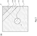
- Fig. 2 is a top-view diagram of a light-emitting diode chip according to one embodiment of this invention.
- a light-emitting diode chip 200 includes a first semiconductor layer 312, a second semiconductor layer 314, a third semiconductor layer 316 and a fourth semiconductor layer 318.
- the interface 116 between the second semiconductor layer 314 and the fourth semiconductor layer 318 is a straight line from the top view.
- the second semiconductor layer 314 and the fourth semiconductor layer 318 are next to the interface 116.
- the first semiconductor layer 312 and the second semiconductor layer 314 are components of the light-emitting diode structure.
- the third semiconductor layer 316 and the fourth semiconductor layer 318 are components of the electrostatic discharge protection structure. Other components of the light-emitting diode chip 200 are not shown here for clarity.
- the second semiconductor layer 314 is disposed on the first semiconductor layer 312 and the partial first semiconductor layer 312 is exposed.
- the fourth semiconductor layer 318 is disposed on the third semiconductor layer 316 and the partial third semiconductor layer 316 is exposed. In one embodiment of the invention, a top-view area of the fourth semiconductor layer 318 is larger than 3000 ⁇ m 2 .
- the first semiconductor layer 312 has a first type doping.
- the second semiconductor layer 314 has a second type doping which is different from the first type doping.
- the third semiconductor layer 316 has a first type doping.
- the fourth semiconductor layer 318 has a second type doping which is different from the first type doping.
- the first type doping is n-type doping and the second type doping is p-type doping. In another embodiment of the invention, the first type doping is p-type doping and the second type doping is n-type doping.
- both the first semiconductor layer 312 and the third semiconductor layer 316 are n-type gallium nitride (GaN).
- both the second semiconductor layer 314 and the fourth semiconductor layer 318 are p-type GaN.
- Fig. 3 is a cross-sectional diagram of the light-emitting diode chip along the section line A-A' in Fig. 2 .
- the light-emitting diode chip 300 in Fig. 3 shows these components which are not shown in light-emitting diode chip 200.
- a light-emitting diode structure 314A and an electrostatic discharge protection structure 318B are disposed on a substrate 310.
- the substrate 310 could be, for example, a sapphire substrate.
- the light-emitting diode structure 314A includes the first semiconductor layer 312, a first active layer 313 disposed on the partial first semiconductor layer 312, and the second semiconductor layer 314 disposed on the first active layer 313. As electron-hole recombination occur at the first active layer 313, photons will be generated in the light-emitting diode structure 314A.
- the electrostatic discharge protection structure 318B includes the third semiconductor layer 316, a second active layer 317 disposed on the partial third semiconductor layer 316, and the fourth semiconductor layer 318 disposed on the second active layer 317. In one embodiment of the invention, the second active layer 317 of the electrostatic discharge protection structure 318B could be omitted.
- the first semiconductor layer 312 and the third semiconductor layer 316 are fabricated from the same semiconductor layer
- the second semiconductor layer 314 and the fourth semiconductor layer 318 are fabricated from the same semiconductor layer
- the first active layer 313 and the second active layer 317 are fabricated from the same active layer.
- the interface includes a connection region including all components which are surrounded by a first surface 382, a second surface 384, and an upper surface 386 of the substrate 310.
- the first surface 382 extends from the upper surface 386 of the substrate 310 to an upper surface of the second semiconductor layer 314.
- the second surface 384 extends from the upper surface 386 of the substrate 310 to an upper surface of the fourth semiconductor layer 318.
- the connection region includes a first protective layer 320, a first wire 330, a second protective layer 340 and a second wire 350.
- the first protective layer 320 is used to insulate the light-emitting diode structure 314A from the electrostatic discharge protection structure 318B.
- the first protective layer 320 could be, for instance, a passivation layer or an insulating layer.
- the first wire 330 covers the first protective layer 320, and extends onto both the first semiconductor layer 312 and the fourth semiconductor layer 318. Moreover, due to the continuity of the structure of the first wire 330, the first semiconductor layer 312 could be electrically connected to the fourth semiconductor layer 318.
- the second protective layer 340 is disposed on the first wire 330, and the second wire 350 is disposed on the second protective layer 340.
- the second wire 350 extends onto the second semiconductor layer 314 and the third semiconductor layer 316 and electrically connects the second semiconductor layer 314 with the third semiconductor layer 316.
- the light-emitting diode structure 314A electrically connects the electrostatic discharge protection structure 318B through the connection region.
- both the second semiconductor layer 314 and the fourth semiconductor layer 318 are next to the connection region.
- the light-emitting diode chip 300 in Fig. 3 retains smaller uncovered top-view area of the third semiconductor layer 316, with other area overlaid with the fourth semiconductor layer 318.
- This design results in smaller top-view area of the electrostatic discharge protection structure 318B, leading to larger top-view area of the light-emitting diode structure 314A and further increasing the brightness of the light-emitting diode chip 300.
- the first wire 330 is connected with the fourth semiconductor layer 318 through a second barrier layer 360b and a second mirror layer 370b.
- the invention is not limited to the illustrative embodiment.
- the first wire 330 could be directly connected to the fourth semiconductor layer 318 by omitting the second barrier layer 360b and the second mirror layer 370b.
- the second wire 350 is connected with the second semiconductor layer 314 through a first barrier layer 360a and a first mirror layer 370a.
- the invention is not limited to the illustrative embodiment.
- the second wire 350 could be directly connected to the second semiconductor layer 314 by omitting the first barrier layer 360a and the first mirror layer 370a.
- Figs. 4A-4B are top-view diagrams of light-emitting diode chips according to one embodiment of this invention.
- a light-emitting diode chip 410 includes a connection region between the light-emitting diode structure 112 and the electrostatic discharge protection structure 114 as shown in Fig. 4A . Only partial components in the connection region are shown here for clarity.
- the first protective layer 320 is entirely covered with the first wire 330. As a result, the first protective layer 320 could not be observed from the top view.
- the structural design of the light-emitting diode chip 410 could enhance the luminance of the light-emitting diode chip 410 and make the current flowing through the light-emitting diode structure 112 and the electrostatic discharge protection structure 114 more homogeneous.
- a light-emitting diode chip 420 includes a connection region between the light-emitting diode structure 112 and the electrostatic discharge protection structure 114 as shown in Fig. 4B . Only partial components in the connection region are shown here for clarity. As shown in Fig. 4B , the first wire 330 partially covers the electrostatic discharge protection structure 320 in the connection region. Therefore, part of the first protective layer 320 is exposed from the top view. Since the first protective layer 320 is partially covered with the first wire 330, it would decrease the possibility of occurring leakage current in the connection region. According to the embodiments illustrated by Figs. 4A-4B , the degree of covering the first protective 320 with the first wire 330 is adjustable to satisfy design requirements of different light-emitting diode chips.
- the invention provides the light-emitting diode chips including the light-emitting diode structure and the electrostatic discharge protection structure. Since the interface between the two structures is a straight line from the top view, the luminance, yield and electrical performance of the light-emitting diode chip are improved. Also, the possibility of occurring leakage current is reduced and thus the high-quality light-emitting diode chip is obtained.
- the invention is defined by the appended claims.
Landscapes
- Led Device Packages (AREA)
- Led Devices (AREA)
Description
- The present invention relates to a semiconductor component. More particularly, the present invention relates to a light-emitting diode chip.
- During processes of fabricating, assembling and examining light-emitting diode chips, electrostatic charges often accumulate within the light-emitting diode chips. As the electrostatic charges accumulate to a certain extent, an electrostatic discharge would occur. Due to the high voltage, short discharge time, and large instant current of the electrostatic discharge, it would cause damage to the circuit function of the light-emitting diode chips.
- For preventing the damage caused by the electrostatic discharge, electrostatic discharge (ESD) protection structures are often disposed in the light-emitting diode chips; however, the electrostatic discharge protection structures would lead to a reduction in the light-emitting area of the light-emitting diode chips, and degrade the yield and the quantity of light-emitting diode chips at the same time. As a result, new light-emitting diode chips are required.
-
US 2015/0091041 A1 describes a semiconductor light emitting device which has an improved withstand voltage against reserve ESD and a semiconductor light emitting apparatus including the same. -
US 2012/0062638 A1 describes a semiconductor light emitting device which has a structure in which an ESD protection diode is integrated therewith. -
US 2015/0349232 A1 describes light emitting diodes and light emitting devices which includes the same to improve luminous efficacy and heat dissipation efficiency. - The invention provides a light-emitting diode chip. The light-emitting diode chip includes a light-emitting diode structure and an electrostatic discharge (ESD) protection structure. The electrostatic discharge protection structure is in a corner of the light-emitting diode chip and connects with the light-emitting diode structure in anti-parallel. An interface between the light-emitting diode structure and the electrostatic discharge protection structure is a straight line from a top view. A top-view outline of the electrostatic discharge protection structure is triangular.
- In one embodiment of the invention, a top-view area of the electrostatic discharge protection structure is 0.5-30% of a top-view area of the light-emitting diode structure.
- In one embodiment of the invention, the light-emitting diode structure includes a first semiconductor layer, a first active layer, and a second semiconductor layer. The first semiconductor layer has a first type doping. The first active layer is disposed on the partial first semiconductor layer. The second semiconductor layer disposed on the first active layer is next to the interface and has a second type doping different from the first type doping.
- In one embodiment of the invention, the electrostatic discharge protection structure includes a third semiconductor layer, a second active layer, and a fourth semiconductor layer. The third semiconductor layer has the first type doping. The second active layer is disposed on the partial third semiconductor layer. The fourth semiconductor layer disposed on the second active layer is next to the interface and has the second type doping.
- In one embodiment of the invention, the first type doping is n-type doping and the second type doping is p-type doping.
- In one embodiment of the invention, the interface includes a connection region. The connection region includes a first protective layer, a first wire, a second protective layer, and a second wire. The first protective layer insulates the light-emitting diode structure from the electrostatic discharge protection structure. The first wire covers the first protective layer, extends onto the first semiconductor layer and the fourth semiconductor layer, and electrically connects the first semiconductor layer with the fourth semiconductor layer. The second protective layer is disposed on the first wire. The second wire is disposed on the second protective layer, extends onto the second semiconductor layer and the third semiconductor layer, and electrically connects the second semiconductor layer with the third semiconductor layer.
- In one embodiment of the invention, the first wire partially covers the first protective layer.
- In one embodiment of the invention, the light-emitting diode chip further includes a first barrier layer between the second wire and the second semiconductor layer; and a second barrier layer between the second wire and the fourth semiconductor layer.
- In one embodiment of the invention, the electrostatic discharge protection structure comprises a Zener diode or a Schottky diode.
- The invention can be more fully understood by reading the following detailed description of the embodiment, with reference made to the accompanying drawings as follows:
-
Figs. 1A-1D are top-view diagrams of light-emitting diode chips according to one embodiment of this invention; -
Fig. 2 is a top-view diagram of a light-emitting diode chip according to one embodiment of this invention; -
Fig. 3 is a cross-sectional diagram of the light-emitting diode chip along the section line A-A' inFig. 2 ; and -
Figs. 4A-4B are top-view diagrams of light-emitting diode chips according to one embodiment of this invention. - The following embodiments are disclosed with accompanying diagrams for detailed description. For illustration clarity, many details of practice are explained in the following descriptions. However, it should be understood that these details of practice do not intend to limit the present invention. That is, these details of practice are not necessary in parts of embodiments of the present invention. Furthermore, for simplifying the drawings, some of the conventional structures and elements are shown with schematic illustrations.
- The terminology used herein is for the purpose of describing particular embodiments only and is not intended to be limiting of the invention. As used herein, the singular forms "a", "an" and "the" are intended to include the plural forms as well, unless the context clearly indicates otherwise. It will be further understood that the terms "comprises" and/or "comprising", or "includes" and/or "including" or "has" and/or "having" when used in this specification, specify the presence of stated features, regions, integers, steps, operations, elements, and/or components, but do not preclude the presence or addition of one or more other features, regions, integers, steps, operations, elements, components, and/or groups thereof.
- It will be understood that when an element is referred to as being "connected" or "coupled" to another element, it can be directly connected or coupled to the other element or intervening elements may be present. In contrast, when an element is referred to as being "directly connected" or "directly coupled" to another element, there are no intervening elements present.
- Please refer to
Figs. 1A-1D. Figs. 1A-1D are top-view diagrams of light-emitting diode chips according to one embodiment of this invention. As shown inFig. 1A , a light-emitting diode chip 110 includes a light-emitting diode structure 112 and an electrostatic discharge protection (ESD)structure 114, which is used to avoid damages caused by electrostatic discharge. The electrostaticdischarge protection structure 114 is disposed in a corner of the light-emittingdiode chip 110 and connects with the light-emittingdiode structure 112 in anti-parallel. Aninterface 116 between the light-emitting diode structure 112 and the electrostaticdischarge protection structure 114 is a straight line from a top view. It is worth noting that because the light-emittingdiode structure 112 and the electrostaticdischarge protection structure 114 are connected in anti-parallel, current could flow out from the electrostaticdischarge protection structure 114 without causing damages to the light-emittingdiode structure 112 as encountering the electrostatic discharge. - In one embodiment of the invention, the electrostatic discharge protection structure includes a Zener diode or a Schottky diode.
- Through many kinds of electrically connecting components, the light-emitting
diode structure 112 could connect with the electrostaticdischarge protection structure 114 in anti-parallel. For example, electrically connecting components include wire bondings, bonding pads, or conducting materials disposed in theinterface 116. Therefore, depending on the different design requirements, insulating materials can be disposed in theinterface 116 for insulating the light-emittingdiode structure 112 from the electrostaticdischarge protection structure 114. Unnecessary details are not provided here. - As shown in
Fig. 1A , it is worth noting that theinterface 116 between the light-emittingdiode structure 112 and the electrostaticdischarge protection structure 114 is a straight line from a top view, namely, theinterface 116 is not circuitous from a top view. Compared with circuitous or zigzag interfaces, theinterface 116 could reduce the possibility of occurring leakage current, further enhancing the quantity, yield and electrical performance of the light-emitting diode chip. Besides, owing to an insulating requirement between the light-emittingdiode structure 112 and the electrostaticdischarge protection structure 114, there must exist some interfaces, of which the simplest form is a straight line. Accordingly, the straight-line design of theinterface 116 would minimize contact area between the light-emittingdiode structure 112 and the electrostaticdischarge protection structure 114, further abating problems of the interface blocking the emergent light and enhancing the luminous efficacy of the light-emitting diode chip accordingly. - In one embodiment of the invention, a light-emitting diode chip may include a plurality of electrostatic discharge protection structures. Depending on the different design requirements, the numbers and positions of the electrostatic discharge protection structures are freely adjustable. As shown in
Fig. 1B , a light-emittingdiode chip 120 includes two electrostaticdischarge protection structures 114. As shown inFig. 1C , a light-emittingdiode chip 130 includes three electrostaticdischarge protection structures 114. As shown inFig. 1D , a light-emittingdiode chip 140 includes four electrostaticdischarge protection structures 114. - The present invention illustratively shows the light-emitting
diode chip 110, the light-emittingdiode chip 120, the light-emittingdiode chip 130 and the light-emittingdiode chip 140 are rectangular. Furthermore, in one embodiment of the invention, a top-view outline of the electrostaticdischarge protection structure 114 is triangular. Compared with rectangular electrostatic discharge protection structures, a top-view area of the electrostaticdischarge protection structure 114 is smaller, such that a top-view area of the light-emittingdiode structure 112 increases and the light-emitting area of the light-emittingdiode structure 112 is larger accordingly. However, the shape of the light-emitting diode chip is arbitrary and is not limited to the illustrative figures in the invention. - In one embodiment of the invention, a top-view area of an electrostatic discharge protection structure is 0.5-30% of a top-view area of a light-emitting diode structure.
- Please refer to
Fig. 2. Fig. 2 is a top-view diagram of a light-emitting diode chip according to one embodiment of this invention. As shown inFig. 2 , a light-emittingdiode chip 200 includes afirst semiconductor layer 312, asecond semiconductor layer 314, athird semiconductor layer 316 and afourth semiconductor layer 318. Theinterface 116 between thesecond semiconductor layer 314 and thefourth semiconductor layer 318 is a straight line from the top view. Thesecond semiconductor layer 314 and thefourth semiconductor layer 318 are next to theinterface 116. - The
first semiconductor layer 312 and thesecond semiconductor layer 314 are components of the light-emitting diode structure. Thethird semiconductor layer 316 and thefourth semiconductor layer 318 are components of the electrostatic discharge protection structure. Other components of the light-emittingdiode chip 200 are not shown here for clarity. Thesecond semiconductor layer 314 is disposed on thefirst semiconductor layer 312 and the partialfirst semiconductor layer 312 is exposed. Thefourth semiconductor layer 318 is disposed on thethird semiconductor layer 316 and the partialthird semiconductor layer 316 is exposed. In one embodiment of the invention, a top-view area of thefourth semiconductor layer 318 is larger than 3000 µm2. - In one embodiment of the invention, the
first semiconductor layer 312 has a first type doping. On the other hand, thesecond semiconductor layer 314 has a second type doping which is different from the first type doping. In one embodiment of the invention, thethird semiconductor layer 316 has a first type doping. On the other hand, thefourth semiconductor layer 318 has a second type doping which is different from the first type doping. - In one embodiment of the invention, the first type doping is n-type doping and the second type doping is p-type doping. In another embodiment of the invention, the first type doping is p-type doping and the second type doping is n-type doping. For instance, both the
first semiconductor layer 312 and thethird semiconductor layer 316 are n-type gallium nitride (GaN). On the other hand, both thesecond semiconductor layer 314 and thefourth semiconductor layer 318 are p-type GaN. - Please refer to
Fig. 3. Fig. 3 is a cross-sectional diagram of the light-emitting diode chip along the section line A-A' inFig. 2 . The light-emittingdiode chip 300 inFig. 3 shows these components which are not shown in light-emittingdiode chip 200. As shown inFig. 3 , a light-emittingdiode structure 314A and an electrostaticdischarge protection structure 318B are disposed on asubstrate 310. Thesubstrate 310 could be, for example, a sapphire substrate. The light-emittingdiode structure 314A includes thefirst semiconductor layer 312, a firstactive layer 313 disposed on the partialfirst semiconductor layer 312, and thesecond semiconductor layer 314 disposed on the firstactive layer 313. As electron-hole recombination occur at the firstactive layer 313, photons will be generated in the light-emittingdiode structure 314A. On the other hand, the electrostaticdischarge protection structure 318B includes thethird semiconductor layer 316, a secondactive layer 317 disposed on the partialthird semiconductor layer 316, and thefourth semiconductor layer 318 disposed on the secondactive layer 317. In one embodiment of the invention, the secondactive layer 317 of the electrostaticdischarge protection structure 318B could be omitted. - In one embodiment of the invention, during processes of fabricating light-emitting diode chips, the
first semiconductor layer 312 and thethird semiconductor layer 316 are fabricated from the same semiconductor layer, thesecond semiconductor layer 314 and thefourth semiconductor layer 318 are fabricated from the same semiconductor layer, and the firstactive layer 313 and the secondactive layer 317 are fabricated from the same active layer. - In one embodiment of the invention, the interface includes a connection region including all components which are surrounded by a
first surface 382, asecond surface 384, and anupper surface 386 of thesubstrate 310. Thefirst surface 382 extends from theupper surface 386 of thesubstrate 310 to an upper surface of thesecond semiconductor layer 314. Thesecond surface 384 extends from theupper surface 386 of thesubstrate 310 to an upper surface of thefourth semiconductor layer 318. Specifically, the connection region includes a firstprotective layer 320, afirst wire 330, a secondprotective layer 340 and asecond wire 350. - The first
protective layer 320 is used to insulate the light-emittingdiode structure 314A from the electrostaticdischarge protection structure 318B. The firstprotective layer 320 could be, for instance, a passivation layer or an insulating layer. Thefirst wire 330 covers the firstprotective layer 320, and extends onto both thefirst semiconductor layer 312 and thefourth semiconductor layer 318. Moreover, due to the continuity of the structure of thefirst wire 330, thefirst semiconductor layer 312 could be electrically connected to thefourth semiconductor layer 318. On the other hand, the secondprotective layer 340 is disposed on thefirst wire 330, and thesecond wire 350 is disposed on the secondprotective layer 340. Thesecond wire 350 extends onto thesecond semiconductor layer 314 and thethird semiconductor layer 316 and electrically connects thesecond semiconductor layer 314 with thethird semiconductor layer 316. In other words, the light-emittingdiode structure 314A electrically connects the electrostaticdischarge protection structure 318B through the connection region. - As shown in
Fig. 3 , both thesecond semiconductor layer 314 and thefourth semiconductor layer 318 are next to the connection region. In comparison with thefourth semiconductor layer 318 which is distant from the connection region, the light-emittingdiode chip 300 inFig. 3 retains smaller uncovered top-view area of thethird semiconductor layer 316, with other area overlaid with thefourth semiconductor layer 318. This design results in smaller top-view area of the electrostaticdischarge protection structure 318B, leading to larger top-view area of the light-emittingdiode structure 314A and further increasing the brightness of the light-emittingdiode chip 300. - In one embodiment of the invention, the
first wire 330 is connected with thefourth semiconductor layer 318 through asecond barrier layer 360b and asecond mirror layer 370b. However, the invention is not limited to the illustrative embodiment. Thefirst wire 330 could be directly connected to thefourth semiconductor layer 318 by omitting thesecond barrier layer 360b and thesecond mirror layer 370b. - In one embodiment of the invention, the
second wire 350 is connected with thesecond semiconductor layer 314 through afirst barrier layer 360a and afirst mirror layer 370a. However, the invention is not limited to the illustrative embodiment. Thesecond wire 350 could be directly connected to thesecond semiconductor layer 314 by omitting thefirst barrier layer 360a and thefirst mirror layer 370a. - Please refer to the
Figs. 4A-4B. Figs. 4A-4B are top-view diagrams of light-emitting diode chips according to one embodiment of this invention. In one embodiment of the invention, a light-emittingdiode chip 410 includes a connection region between the light-emittingdiode structure 112 and the electrostaticdischarge protection structure 114 as shown inFig. 4A . Only partial components in the connection region are shown here for clarity. As shown inFig. 4A , the firstprotective layer 320 is entirely covered with thefirst wire 330. As a result, the firstprotective layer 320 could not be observed from the top view. Since thefirst wire 330 totally covers the firstprotective layer 320 and thefirst wire 330 is capable of reflecting light from active layer, the structural design of the light-emittingdiode chip 410 could enhance the luminance of the light-emittingdiode chip 410 and make the current flowing through the light-emittingdiode structure 112 and the electrostaticdischarge protection structure 114 more homogeneous. - In another embodiment of the invention, a light-emitting
diode chip 420 includes a connection region between the light-emittingdiode structure 112 and the electrostaticdischarge protection structure 114 as shown inFig. 4B . Only partial components in the connection region are shown here for clarity. As shown inFig. 4B , thefirst wire 330 partially covers the electrostaticdischarge protection structure 320 in the connection region. Therefore, part of the firstprotective layer 320 is exposed from the top view. Since the firstprotective layer 320 is partially covered with thefirst wire 330, it would decrease the possibility of occurring leakage current in the connection region. According to the embodiments illustrated byFigs. 4A-4B , the degree of covering the first protective 320 with thefirst wire 330 is adjustable to satisfy design requirements of different light-emitting diode chips. - In summary, the invention provides the light-emitting diode chips including the light-emitting diode structure and the electrostatic discharge protection structure. Since the interface between the two structures is a straight line from the top view, the luminance, yield and electrical performance of the light-emitting diode chip are improved. Also, the possibility of occurring leakage current is reduced and thus the high-quality light-emitting diode chip is obtained. The invention is defined by the appended claims.
Claims (9)
- A light-emitting diode chip (110, 120, 130, 140, 200, 300, 410, 420), comprising:a light-emitting diode structure (112, 314A); andan electrostatic discharge protection structure (114, 318B) in a corner of the light-emitting diode chip (110, 120, 130, 140, 200, 300, 410, 420) and connecting with the light-emitting diode structure (112, 314A) in anti-parallel, wherein an interface (116) between the light-emitting diode structure (112, 314A) and the electrostatic discharge protection structure (114, 318B) is a straight line from a top view, characterized in thata top-view outline of the electrostatic discharge protection structure (114, 318B) is triangular.
- The light-emitting diode chip of claim 1, wherein a top-view area of the electrostatic discharge protection structure (114, 318B) is 0.5-30% of a top-view area of the light-emitting diode structure (112, 314A).
- The light-emitting diode chip of claim 1, wherein the light-emitting diode structure (314A) comprises:a first semiconductor layer (312) having a first type doping;a first active layer (313) disposed on the partial first semiconductor layer (312); anda second semiconductor layer (314) disposed on the first active layer (313), having a second type doping different from the first type doping, and being next to the interface (116).
- The light-emitting diode chip of claim 3, wherein the electrostatic discharge protection structure (318B) comprises:a third semiconductor layer (316) having the first type doping;a second active layer (317) disposed on the partial third semiconductor layer (316); anda fourth semiconductor layer (318) disposed on the second active layer (317), having the second type doping, and being next to the interface (116).
- The light-emitting diode chip of claim 3, wherein the first type doping is n-type doping and the second type doping is p-type doping.
- The light-emitting diode chip of claim 4, wherein the interface (116) comprises a connection region and the connection region comprises:a first protective layer (320) insulating the light-emitting diode structure (314A) from the electrostatic discharge protection structure (318B);a first wire (330) covering the first protective layer (320), extending onto the first semiconductor layer (312) and the fourth semiconductor layer (318), and electrically connecting the first semiconductor layer (312) with the fourth semiconductor layer (318);a second protective layer (340) disposed on the first wire (330); anda second wire (350) disposed on the second protective layer (340), extending onto the second semiconductor layer (314) and the third semiconductor layer (316), and electrically connecting the second semiconductor layer (314) with the third semiconductor layer (316).
- The light-emitting diode chip of claim 6, wherein the first wire 330 partially covers the first protective layer (320).
- The light-emitting diode chip of claim 6, further comprising:a first barrier layer (360a) between the second wire (350) and the second semiconductor layer (314); anda second barrier layer (360b) between the second wire (350) and the fourth semiconductor layer (318).
- The light-emitting diode chip of claim 1, wherein the electrostatic discharge protection structure (114) comprises a Zener diode or a Schottky diode.
Applications Claiming Priority (1)
| Application Number | Priority Date | Filing Date | Title |
|---|---|---|---|
| TW104144505A TWI578576B (en) | 2015-12-30 | 2015-12-30 | Light-emitting diode chip |
Publications (2)
| Publication Number | Publication Date |
|---|---|
| EP3188241A1 EP3188241A1 (en) | 2017-07-05 |
| EP3188241B1 true EP3188241B1 (en) | 2018-06-27 |
Family
ID=57614266
Family Applications (1)
| Application Number | Title | Priority Date | Filing Date |
|---|---|---|---|
| EP16207073.4A Active EP3188241B1 (en) | 2015-12-30 | 2016-12-28 | Light-emitting diode chip |
Country Status (4)
| Country | Link |
|---|---|
| US (1) | US10283497B2 (en) |
| EP (1) | EP3188241B1 (en) |
| KR (1) | KR20170080471A (en) |
| TW (1) | TWI578576B (en) |
Families Citing this family (3)
| Publication number | Priority date | Publication date | Assignee | Title |
|---|---|---|---|---|
| US8471282B2 (en) * | 2010-06-07 | 2013-06-25 | Koninklijke Philips Electronics N.V. | Passivation for a semiconductor light emitting device |
| CN113363359A (en) * | 2021-06-09 | 2021-09-07 | 泉州三安半导体科技有限公司 | Flip-chip light emitting diode |
| JP7662754B2 (en) * | 2022-12-29 | 2025-04-15 | エルジー ディスプレイ カンパニー リミテッド | Display panel and display device including the same |
Family Cites Families (13)
| Publication number | Priority date | Publication date | Assignee | Title |
|---|---|---|---|---|
| TW492202B (en) | 2001-06-05 | 2002-06-21 | South Epitaxy Corp | Structure of III-V light emitting diode (LED) arranged in flip chip configuration having structure for preventing electrostatic discharge |
| TWI229463B (en) | 2004-02-02 | 2005-03-11 | South Epitaxy Corp | Light-emitting diode structure with electro-static discharge protection |
| US20050179042A1 (en) | 2004-02-13 | 2005-08-18 | Kopin Corporation | Monolithic integration and enhanced light extraction in gallium nitride-based light-emitting devices |
| KR100576872B1 (en) * | 2004-09-17 | 2006-05-10 | 삼성전기주식회사 | Nitride semiconductor light emitting device having anti-static discharge function |
| TWI257186B (en) * | 2005-09-29 | 2006-06-21 | Formosa Epitaxy Inc | Light-emitting diode chip |
| DE102007061479A1 (en) | 2007-12-20 | 2009-06-25 | Osram Opto Semiconductors Gmbh | LED chip with surge protection |
| KR101428085B1 (en) * | 2008-07-24 | 2014-08-07 | 엘지이노텍 주식회사 | Semiconductor light emitting device and fabrication method thereof |
| JP2012023328A (en) * | 2010-06-18 | 2012-02-02 | Citizen Holdings Co Ltd | Semiconductor light-emitting element and manufacturing method of the same |
| US8723206B2 (en) | 2011-09-09 | 2014-05-13 | Samsung Electronics Co., Ltd. | Semiconductor light emitting device with contact hole passing through active layer |
| CN202871793U (en) | 2012-10-13 | 2013-04-10 | 江苏新广联科技股份有限公司 | Light emitting diode structure with improved electrostatic protection |
| US8835949B2 (en) * | 2013-02-21 | 2014-09-16 | Sharp Laboratories Of America, Inc. | Three-terminal light emitting device (LED) with built-in electrostatic discharge (ESD) protection device |
| KR20150035656A (en) | 2013-09-27 | 2015-04-07 | 삼성전자주식회사 | Semiconductor light emitting device and semiconductor light emitting apparatus having the same |
| US9728698B2 (en) | 2014-06-03 | 2017-08-08 | Seoul Viosys Co., Ltd. | Light emitting device package having improved heat dissipation efficiency |
-
2015
- 2015-12-30 TW TW104144505A patent/TWI578576B/en active
-
2016
- 2016-11-27 US US15/361,475 patent/US10283497B2/en active Active
- 2016-12-06 KR KR1020160164781A patent/KR20170080471A/en not_active Ceased
- 2016-12-28 EP EP16207073.4A patent/EP3188241B1/en active Active
Non-Patent Citations (1)
| Title |
|---|
| None * |
Also Published As
| Publication number | Publication date |
|---|---|
| TW201724565A (en) | 2017-07-01 |
| EP3188241A1 (en) | 2017-07-05 |
| TWI578576B (en) | 2017-04-11 |
| KR20170080471A (en) | 2017-07-10 |
| US20170194313A1 (en) | 2017-07-06 |
| US10283497B2 (en) | 2019-05-07 |
Similar Documents
| Publication | Publication Date | Title |
|---|---|---|
| JP5015433B2 (en) | LED chip with built-in high-speed switching diode for ESD protection | |
| US7683383B2 (en) | Light emitting device having circuit protection unit | |
| US7105860B2 (en) | Flip chip light-emitting diode package | |
| US8129726B2 (en) | Light-emitting diode package having electrostatic discharge protection function and method of fabricating the same | |
| US7750439B2 (en) | ESD protection device | |
| US9929315B2 (en) | LED chip resistant to electrostatic discharge and LED package including the same | |
| US20060267040A1 (en) | High-brightness LED with protective function of electrostatic discharge damage | |
| CN105531834B (en) | LED chips with ESD protection | |
| US7589350B2 (en) | Light-emitting diode chip | |
| KR101039939B1 (en) | Light emitting device, method of manufacturing light emitting device, light emitting device package and lighting system including same | |
| JP3559435B2 (en) | Semiconductor light emitting device | |
| JPH1154804A (en) | Chip type light emitting device | |
| US20100207163A1 (en) | Semiconductor device including electrostatic-discharge protection circuit | |
| US10283497B2 (en) | Light-emitting diode chip | |
| US20160300829A1 (en) | Optoelectronic semiconductor chip with built-in esd protection | |
| US20150249072A1 (en) | Optoelectronic Component and Method for Producing an Optoelectronic Component | |
| CN115312514B (en) | Transient Voltage Suppression Device | |
| CN114551435B (en) | Bidirectional electrostatic discharge protection device | |
| US9685396B2 (en) | Semiconductor die arrangement | |
| EP2851946A1 (en) | Surge protection device | |
| KR20150042012A (en) | Light emitting diode array | |
| US20120003762A1 (en) | Method to Protect Compound Semiconductor from Electrostatic Discharge Damage | |
| US12224279B2 (en) | Integrated mult-device chip and package | |
| KR20160128516A (en) | Semiconductor light emitting device package | |
| US9048278B2 (en) | Semiconductor device |
Legal Events
| Date | Code | Title | Description |
|---|---|---|---|
| PUAI | Public reference made under article 153(3) epc to a published international application that has entered the european phase |
Free format text: ORIGINAL CODE: 0009012 |
|
| AK | Designated contracting states |
Kind code of ref document: A1 Designated state(s): AL AT BE BG CH CY CZ DE DK EE ES FI FR GB GR HR HU IE IS IT LI LT LU LV MC MK MT NL NO PL PT RO RS SE SI SK SM TR |
|
| AX | Request for extension of the european patent |
Extension state: BA ME |
|
| 17P | Request for examination filed |
Effective date: 20180103 |
|
| RBV | Designated contracting states (corrected) |
Designated state(s): AL AT BE BG CH CY CZ DE DK EE ES FI FR GB GR HR HU IE IS IT LI LT LU LV MC MK MT NL NO PL PT RO RS SE SI SK SM TR |
|
| GRAP | Despatch of communication of intention to grant a patent |
Free format text: ORIGINAL CODE: EPIDOSNIGR1 |
|
| RIC1 | Information provided on ipc code assigned before grant |
Ipc: H01L 33/38 20100101ALN20180212BHEP Ipc: H01L 27/15 20060101AFI20180212BHEP |
|
| INTG | Intention to grant announced |
Effective date: 20180227 |
|
| GRAS | Grant fee paid |
Free format text: ORIGINAL CODE: EPIDOSNIGR3 |
|
| GRAA | (expected) grant |
Free format text: ORIGINAL CODE: 0009210 |
|
| AK | Designated contracting states |
Kind code of ref document: B1 Designated state(s): AL AT BE BG CH CY CZ DE DK EE ES FI FR GB GR HR HU IE IS IT LI LT LU LV MC MK MT NL NO PL PT RO RS SE SI SK SM TR |
|
| REG | Reference to a national code |
Ref country code: GB Ref legal event code: FG4D |
|
| REG | Reference to a national code |
Ref country code: AT Ref legal event code: REF Ref document number: 1013064 Country of ref document: AT Kind code of ref document: T Effective date: 20180715 |
|
| REG | Reference to a national code |
Ref country code: IE Ref legal event code: FG4D |
|
| REG | Reference to a national code |
Ref country code: DE Ref legal event code: R096 Ref document number: 602016003844 Country of ref document: DE |
|
| PG25 | Lapsed in a contracting state [announced via postgrant information from national office to epo] |
Ref country code: NO Free format text: LAPSE BECAUSE OF FAILURE TO SUBMIT A TRANSLATION OF THE DESCRIPTION OR TO PAY THE FEE WITHIN THE PRESCRIBED TIME-LIMIT Effective date: 20180927 Ref country code: LT Free format text: LAPSE BECAUSE OF FAILURE TO SUBMIT A TRANSLATION OF THE DESCRIPTION OR TO PAY THE FEE WITHIN THE PRESCRIBED TIME-LIMIT Effective date: 20180627 Ref country code: FI Free format text: LAPSE BECAUSE OF FAILURE TO SUBMIT A TRANSLATION OF THE DESCRIPTION OR TO PAY THE FEE WITHIN THE PRESCRIBED TIME-LIMIT Effective date: 20180627 Ref country code: SE Free format text: LAPSE BECAUSE OF FAILURE TO SUBMIT A TRANSLATION OF THE DESCRIPTION OR TO PAY THE FEE WITHIN THE PRESCRIBED TIME-LIMIT Effective date: 20180627 Ref country code: BG Free format text: LAPSE BECAUSE OF FAILURE TO SUBMIT A TRANSLATION OF THE DESCRIPTION OR TO PAY THE FEE WITHIN THE PRESCRIBED TIME-LIMIT Effective date: 20180927 |
|
| REG | Reference to a national code |
Ref country code: NL Ref legal event code: MP Effective date: 20180627 |
|
| REG | Reference to a national code |
Ref country code: LT Ref legal event code: MG4D |
|
| PG25 | Lapsed in a contracting state [announced via postgrant information from national office to epo] |
Ref country code: GR Free format text: LAPSE BECAUSE OF FAILURE TO SUBMIT A TRANSLATION OF THE DESCRIPTION OR TO PAY THE FEE WITHIN THE PRESCRIBED TIME-LIMIT Effective date: 20180928 Ref country code: LV Free format text: LAPSE BECAUSE OF FAILURE TO SUBMIT A TRANSLATION OF THE DESCRIPTION OR TO PAY THE FEE WITHIN THE PRESCRIBED TIME-LIMIT Effective date: 20180627 Ref country code: RS Free format text: LAPSE BECAUSE OF FAILURE TO SUBMIT A TRANSLATION OF THE DESCRIPTION OR TO PAY THE FEE WITHIN THE PRESCRIBED TIME-LIMIT Effective date: 20180627 Ref country code: HR Free format text: LAPSE BECAUSE OF FAILURE TO SUBMIT A TRANSLATION OF THE DESCRIPTION OR TO PAY THE FEE WITHIN THE PRESCRIBED TIME-LIMIT Effective date: 20180627 |
|
| REG | Reference to a national code |
Ref country code: AT Ref legal event code: MK05 Ref document number: 1013064 Country of ref document: AT Kind code of ref document: T Effective date: 20180627 |
|
| PG25 | Lapsed in a contracting state [announced via postgrant information from national office to epo] |
Ref country code: NL Free format text: LAPSE BECAUSE OF FAILURE TO SUBMIT A TRANSLATION OF THE DESCRIPTION OR TO PAY THE FEE WITHIN THE PRESCRIBED TIME-LIMIT Effective date: 20180627 |
|
| PG25 | Lapsed in a contracting state [announced via postgrant information from national office to epo] |
Ref country code: CZ Free format text: LAPSE BECAUSE OF FAILURE TO SUBMIT A TRANSLATION OF THE DESCRIPTION OR TO PAY THE FEE WITHIN THE PRESCRIBED TIME-LIMIT Effective date: 20180627 Ref country code: RO Free format text: LAPSE BECAUSE OF FAILURE TO SUBMIT A TRANSLATION OF THE DESCRIPTION OR TO PAY THE FEE WITHIN THE PRESCRIBED TIME-LIMIT Effective date: 20180627 Ref country code: SK Free format text: LAPSE BECAUSE OF FAILURE TO SUBMIT A TRANSLATION OF THE DESCRIPTION OR TO PAY THE FEE WITHIN THE PRESCRIBED TIME-LIMIT Effective date: 20180627 Ref country code: AT Free format text: LAPSE BECAUSE OF FAILURE TO SUBMIT A TRANSLATION OF THE DESCRIPTION OR TO PAY THE FEE WITHIN THE PRESCRIBED TIME-LIMIT Effective date: 20180627 Ref country code: IS Free format text: LAPSE BECAUSE OF FAILURE TO SUBMIT A TRANSLATION OF THE DESCRIPTION OR TO PAY THE FEE WITHIN THE PRESCRIBED TIME-LIMIT Effective date: 20181027 Ref country code: EE Free format text: LAPSE BECAUSE OF FAILURE TO SUBMIT A TRANSLATION OF THE DESCRIPTION OR TO PAY THE FEE WITHIN THE PRESCRIBED TIME-LIMIT Effective date: 20180627 Ref country code: PL Free format text: LAPSE BECAUSE OF FAILURE TO SUBMIT A TRANSLATION OF THE DESCRIPTION OR TO PAY THE FEE WITHIN THE PRESCRIBED TIME-LIMIT Effective date: 20180627 |
|
| PG25 | Lapsed in a contracting state [announced via postgrant information from national office to epo] |
Ref country code: IT Free format text: LAPSE BECAUSE OF FAILURE TO SUBMIT A TRANSLATION OF THE DESCRIPTION OR TO PAY THE FEE WITHIN THE PRESCRIBED TIME-LIMIT Effective date: 20180627 Ref country code: ES Free format text: LAPSE BECAUSE OF FAILURE TO SUBMIT A TRANSLATION OF THE DESCRIPTION OR TO PAY THE FEE WITHIN THE PRESCRIBED TIME-LIMIT Effective date: 20180627 Ref country code: SM Free format text: LAPSE BECAUSE OF FAILURE TO SUBMIT A TRANSLATION OF THE DESCRIPTION OR TO PAY THE FEE WITHIN THE PRESCRIBED TIME-LIMIT Effective date: 20180627 |
|
| REG | Reference to a national code |
Ref country code: DE Ref legal event code: R097 Ref document number: 602016003844 Country of ref document: DE |
|
| PLBE | No opposition filed within time limit |
Free format text: ORIGINAL CODE: 0009261 |
|
| STAA | Information on the status of an ep patent application or granted ep patent |
Free format text: STATUS: NO OPPOSITION FILED WITHIN TIME LIMIT |
|
| PG25 | Lapsed in a contracting state [announced via postgrant information from national office to epo] |
Ref country code: DK Free format text: LAPSE BECAUSE OF FAILURE TO SUBMIT A TRANSLATION OF THE DESCRIPTION OR TO PAY THE FEE WITHIN THE PRESCRIBED TIME-LIMIT Effective date: 20180627 |
|
| 26N | No opposition filed |
Effective date: 20190328 |
|
| PG25 | Lapsed in a contracting state [announced via postgrant information from national office to epo] |
Ref country code: SI Free format text: LAPSE BECAUSE OF FAILURE TO SUBMIT A TRANSLATION OF THE DESCRIPTION OR TO PAY THE FEE WITHIN THE PRESCRIBED TIME-LIMIT Effective date: 20180627 Ref country code: MC Free format text: LAPSE BECAUSE OF FAILURE TO SUBMIT A TRANSLATION OF THE DESCRIPTION OR TO PAY THE FEE WITHIN THE PRESCRIBED TIME-LIMIT Effective date: 20180627 Ref country code: LU Free format text: LAPSE BECAUSE OF NON-PAYMENT OF DUE FEES Effective date: 20181228 |
|
| REG | Reference to a national code |
Ref country code: IE Ref legal event code: MM4A |
|
| REG | Reference to a national code |
Ref country code: BE Ref legal event code: MM Effective date: 20181231 |
|
| PG25 | Lapsed in a contracting state [announced via postgrant information from national office to epo] |
Ref country code: IE Free format text: LAPSE BECAUSE OF NON-PAYMENT OF DUE FEES Effective date: 20181228 Ref country code: FR Free format text: LAPSE BECAUSE OF NON-PAYMENT OF DUE FEES Effective date: 20181231 |
|
| PG25 | Lapsed in a contracting state [announced via postgrant information from national office to epo] |
Ref country code: AL Free format text: LAPSE BECAUSE OF FAILURE TO SUBMIT A TRANSLATION OF THE DESCRIPTION OR TO PAY THE FEE WITHIN THE PRESCRIBED TIME-LIMIT Effective date: 20180627 Ref country code: BE Free format text: LAPSE BECAUSE OF NON-PAYMENT OF DUE FEES Effective date: 20181231 |
|
| PG25 | Lapsed in a contracting state [announced via postgrant information from national office to epo] |
Ref country code: MT Free format text: LAPSE BECAUSE OF NON-PAYMENT OF DUE FEES Effective date: 20181228 |
|
| PG25 | Lapsed in a contracting state [announced via postgrant information from national office to epo] |
Ref country code: TR Free format text: LAPSE BECAUSE OF FAILURE TO SUBMIT A TRANSLATION OF THE DESCRIPTION OR TO PAY THE FEE WITHIN THE PRESCRIBED TIME-LIMIT Effective date: 20180627 |
|
| PG25 | Lapsed in a contracting state [announced via postgrant information from national office to epo] |
Ref country code: PT Free format text: LAPSE BECAUSE OF FAILURE TO SUBMIT A TRANSLATION OF THE DESCRIPTION OR TO PAY THE FEE WITHIN THE PRESCRIBED TIME-LIMIT Effective date: 20180627 |
|
| PG25 | Lapsed in a contracting state [announced via postgrant information from national office to epo] |
Ref country code: CY Free format text: LAPSE BECAUSE OF FAILURE TO SUBMIT A TRANSLATION OF THE DESCRIPTION OR TO PAY THE FEE WITHIN THE PRESCRIBED TIME-LIMIT Effective date: 20180627 Ref country code: MK Free format text: LAPSE BECAUSE OF NON-PAYMENT OF DUE FEES Effective date: 20180627 Ref country code: HU Free format text: LAPSE BECAUSE OF FAILURE TO SUBMIT A TRANSLATION OF THE DESCRIPTION OR TO PAY THE FEE WITHIN THE PRESCRIBED TIME-LIMIT; INVALID AB INITIO Effective date: 20161228 |
|
| REG | Reference to a national code |
Ref country code: CH Ref legal event code: PL |
|
| PG25 | Lapsed in a contracting state [announced via postgrant information from national office to epo] |
Ref country code: LI Free format text: LAPSE BECAUSE OF NON-PAYMENT OF DUE FEES Effective date: 20191231 Ref country code: CH Free format text: LAPSE BECAUSE OF NON-PAYMENT OF DUE FEES Effective date: 20191231 |
|
| GBPC | Gb: european patent ceased through non-payment of renewal fee |
Effective date: 20201228 |
|
| PG25 | Lapsed in a contracting state [announced via postgrant information from national office to epo] |
Ref country code: GB Free format text: LAPSE BECAUSE OF NON-PAYMENT OF DUE FEES Effective date: 20201228 |
|
| REG | Reference to a national code |
Ref country code: DE Ref legal event code: R079 Ref document number: 602016003844 Country of ref document: DE Free format text: PREVIOUS MAIN CLASS: H01L0027150000 Ipc: H10H0029140000 |
|
| PGFP | Annual fee paid to national office [announced via postgrant information from national office to epo] |
Ref country code: DE Payment date: 20251120 Year of fee payment: 10 |