EP3188163B1 - Display device - Google Patents
Display device Download PDFInfo
- Publication number
- EP3188163B1 EP3188163B1 EP15835522.2A EP15835522A EP3188163B1 EP 3188163 B1 EP3188163 B1 EP 3188163B1 EP 15835522 A EP15835522 A EP 15835522A EP 3188163 B1 EP3188163 B1 EP 3188163B1
- Authority
- EP
- European Patent Office
- Prior art keywords
- display device
- guide plate
- light guide
- display
- display panel
- Prior art date
- Legal status (The legal status is an assumption and is not a legal conclusion. Google has not performed a legal analysis and makes no representation as to the accuracy of the status listed.)
- Active
Links
Images



Classifications
-
- G—PHYSICS
- G02—OPTICS
- G02F—OPTICAL DEVICES OR ARRANGEMENTS FOR THE CONTROL OF LIGHT BY MODIFICATION OF THE OPTICAL PROPERTIES OF THE MEDIA OF THE ELEMENTS INVOLVED THEREIN; NON-LINEAR OPTICS; FREQUENCY-CHANGING OF LIGHT; OPTICAL LOGIC ELEMENTS; OPTICAL ANALOGUE/DIGITAL CONVERTERS
- G02F1/00—Devices or arrangements for the control of the intensity, colour, phase, polarisation or direction of light arriving from an independent light source, e.g. switching, gating or modulating; Non-linear optics
- G02F1/01—Devices or arrangements for the control of the intensity, colour, phase, polarisation or direction of light arriving from an independent light source, e.g. switching, gating or modulating; Non-linear optics for the control of the intensity, phase, polarisation or colour
- G02F1/13—Devices or arrangements for the control of the intensity, colour, phase, polarisation or direction of light arriving from an independent light source, e.g. switching, gating or modulating; Non-linear optics for the control of the intensity, phase, polarisation or colour based on liquid crystals, e.g. single liquid crystal display cells
- G02F1/133—Constructional arrangements; Operation of liquid crystal cells; Circuit arrangements
- G02F1/1333—Constructional arrangements; Manufacturing methods
- G02F1/133308—Support structures for LCD panels, e.g. frames or bezels
-
- G—PHYSICS
- G02—OPTICS
- G02B—OPTICAL ELEMENTS, SYSTEMS OR APPARATUS
- G02B6/00—Light guides; Structural details of arrangements comprising light guides and other optical elements, e.g. couplings
- G02B6/0001—Light guides; Structural details of arrangements comprising light guides and other optical elements, e.g. couplings specially adapted for lighting devices or systems
- G02B6/0011—Light guides; Structural details of arrangements comprising light guides and other optical elements, e.g. couplings specially adapted for lighting devices or systems the light guides being planar or of plate-like form
- G02B6/0081—Mechanical or electrical aspects of the light guide and light source in the lighting device peculiar to the adaptation to planar light guides, e.g. concerning packaging
- G02B6/0086—Positioning aspects
- G02B6/0088—Positioning aspects of the light guide or other optical sheets in the package
-
- G—PHYSICS
- G02—OPTICS
- G02F—OPTICAL DEVICES OR ARRANGEMENTS FOR THE CONTROL OF LIGHT BY MODIFICATION OF THE OPTICAL PROPERTIES OF THE MEDIA OF THE ELEMENTS INVOLVED THEREIN; NON-LINEAR OPTICS; FREQUENCY-CHANGING OF LIGHT; OPTICAL LOGIC ELEMENTS; OPTICAL ANALOGUE/DIGITAL CONVERTERS
- G02F1/00—Devices or arrangements for the control of the intensity, colour, phase, polarisation or direction of light arriving from an independent light source, e.g. switching, gating or modulating; Non-linear optics
- G02F1/01—Devices or arrangements for the control of the intensity, colour, phase, polarisation or direction of light arriving from an independent light source, e.g. switching, gating or modulating; Non-linear optics for the control of the intensity, phase, polarisation or colour
- G02F1/13—Devices or arrangements for the control of the intensity, colour, phase, polarisation or direction of light arriving from an independent light source, e.g. switching, gating or modulating; Non-linear optics for the control of the intensity, phase, polarisation or colour based on liquid crystals, e.g. single liquid crystal display cells
- G02F1/133—Constructional arrangements; Operation of liquid crystal cells; Circuit arrangements
- G02F1/1333—Constructional arrangements; Manufacturing methods
- G02F1/1335—Structural association of cells with optical devices, e.g. polarisers or reflectors
- G02F1/133524—Light-guides, e.g. fibre-optic bundles, louvered or jalousie light-guides
-
- G—PHYSICS
- G02—OPTICS
- G02F—OPTICAL DEVICES OR ARRANGEMENTS FOR THE CONTROL OF LIGHT BY MODIFICATION OF THE OPTICAL PROPERTIES OF THE MEDIA OF THE ELEMENTS INVOLVED THEREIN; NON-LINEAR OPTICS; FREQUENCY-CHANGING OF LIGHT; OPTICAL LOGIC ELEMENTS; OPTICAL ANALOGUE/DIGITAL CONVERTERS
- G02F1/00—Devices or arrangements for the control of the intensity, colour, phase, polarisation or direction of light arriving from an independent light source, e.g. switching, gating or modulating; Non-linear optics
- G02F1/01—Devices or arrangements for the control of the intensity, colour, phase, polarisation or direction of light arriving from an independent light source, e.g. switching, gating or modulating; Non-linear optics for the control of the intensity, phase, polarisation or colour
- G02F1/13—Devices or arrangements for the control of the intensity, colour, phase, polarisation or direction of light arriving from an independent light source, e.g. switching, gating or modulating; Non-linear optics for the control of the intensity, phase, polarisation or colour based on liquid crystals, e.g. single liquid crystal display cells
- G02F1/133—Constructional arrangements; Operation of liquid crystal cells; Circuit arrangements
- G02F1/1333—Constructional arrangements; Manufacturing methods
- G02F1/1335—Structural association of cells with optical devices, e.g. polarisers or reflectors
- G02F1/133528—Polarisers
- G02F1/133536—Reflective polarizers
-
- G—PHYSICS
- G02—OPTICS
- G02F—OPTICAL DEVICES OR ARRANGEMENTS FOR THE CONTROL OF LIGHT BY MODIFICATION OF THE OPTICAL PROPERTIES OF THE MEDIA OF THE ELEMENTS INVOLVED THEREIN; NON-LINEAR OPTICS; FREQUENCY-CHANGING OF LIGHT; OPTICAL LOGIC ELEMENTS; OPTICAL ANALOGUE/DIGITAL CONVERTERS
- G02F1/00—Devices or arrangements for the control of the intensity, colour, phase, polarisation or direction of light arriving from an independent light source, e.g. switching, gating or modulating; Non-linear optics
- G02F1/01—Devices or arrangements for the control of the intensity, colour, phase, polarisation or direction of light arriving from an independent light source, e.g. switching, gating or modulating; Non-linear optics for the control of the intensity, phase, polarisation or colour
- G02F1/13—Devices or arrangements for the control of the intensity, colour, phase, polarisation or direction of light arriving from an independent light source, e.g. switching, gating or modulating; Non-linear optics for the control of the intensity, phase, polarisation or colour based on liquid crystals, e.g. single liquid crystal display cells
- G02F1/133—Constructional arrangements; Operation of liquid crystal cells; Circuit arrangements
- G02F1/1333—Constructional arrangements; Manufacturing methods
- G02F1/1335—Structural association of cells with optical devices, e.g. polarisers or reflectors
- G02F1/133553—Reflecting elements
-
- G—PHYSICS
- G09—EDUCATION; CRYPTOGRAPHY; DISPLAY; ADVERTISING; SEALS
- G09F—DISPLAYING; ADVERTISING; SIGNS; LABELS OR NAME-PLATES; SEALS
- G09F9/00—Indicating arrangements for variable information in which the information is built-up on a support by selection or combination of individual elements
-
- G—PHYSICS
- G02—OPTICS
- G02B—OPTICAL ELEMENTS, SYSTEMS OR APPARATUS
- G02B6/00—Light guides; Structural details of arrangements comprising light guides and other optical elements, e.g. couplings
- G02B6/0001—Light guides; Structural details of arrangements comprising light guides and other optical elements, e.g. couplings specially adapted for lighting devices or systems
- G02B6/0011—Light guides; Structural details of arrangements comprising light guides and other optical elements, e.g. couplings specially adapted for lighting devices or systems the light guides being planar or of plate-like form
- G02B6/0081—Mechanical or electrical aspects of the light guide and light source in the lighting device peculiar to the adaptation to planar light guides, e.g. concerning packaging
- G02B6/0085—Means for removing heat created by the light source from the package
-
- G—PHYSICS
- G02—OPTICS
- G02F—OPTICAL DEVICES OR ARRANGEMENTS FOR THE CONTROL OF LIGHT BY MODIFICATION OF THE OPTICAL PROPERTIES OF THE MEDIA OF THE ELEMENTS INVOLVED THEREIN; NON-LINEAR OPTICS; FREQUENCY-CHANGING OF LIGHT; OPTICAL LOGIC ELEMENTS; OPTICAL ANALOGUE/DIGITAL CONVERTERS
- G02F1/00—Devices or arrangements for the control of the intensity, colour, phase, polarisation or direction of light arriving from an independent light source, e.g. switching, gating or modulating; Non-linear optics
- G02F1/01—Devices or arrangements for the control of the intensity, colour, phase, polarisation or direction of light arriving from an independent light source, e.g. switching, gating or modulating; Non-linear optics for the control of the intensity, phase, polarisation or colour
- G02F1/13—Devices or arrangements for the control of the intensity, colour, phase, polarisation or direction of light arriving from an independent light source, e.g. switching, gating or modulating; Non-linear optics for the control of the intensity, phase, polarisation or colour based on liquid crystals, e.g. single liquid crystal display cells
- G02F1/133—Constructional arrangements; Operation of liquid crystal cells; Circuit arrangements
- G02F1/1333—Constructional arrangements; Manufacturing methods
- G02F1/133308—Support structures for LCD panels, e.g. frames or bezels
- G02F1/133314—Back frames
-
- G—PHYSICS
- G02—OPTICS
- G02F—OPTICAL DEVICES OR ARRANGEMENTS FOR THE CONTROL OF LIGHT BY MODIFICATION OF THE OPTICAL PROPERTIES OF THE MEDIA OF THE ELEMENTS INVOLVED THEREIN; NON-LINEAR OPTICS; FREQUENCY-CHANGING OF LIGHT; OPTICAL LOGIC ELEMENTS; OPTICAL ANALOGUE/DIGITAL CONVERTERS
- G02F1/00—Devices or arrangements for the control of the intensity, colour, phase, polarisation or direction of light arriving from an independent light source, e.g. switching, gating or modulating; Non-linear optics
- G02F1/01—Devices or arrangements for the control of the intensity, colour, phase, polarisation or direction of light arriving from an independent light source, e.g. switching, gating or modulating; Non-linear optics for the control of the intensity, phase, polarisation or colour
- G02F1/13—Devices or arrangements for the control of the intensity, colour, phase, polarisation or direction of light arriving from an independent light source, e.g. switching, gating or modulating; Non-linear optics for the control of the intensity, phase, polarisation or colour based on liquid crystals, e.g. single liquid crystal display cells
- G02F1/133—Constructional arrangements; Operation of liquid crystal cells; Circuit arrangements
- G02F1/1333—Constructional arrangements; Manufacturing methods
- G02F1/133308—Support structures for LCD panels, e.g. frames or bezels
- G02F1/13332—Front frames
-
- G—PHYSICS
- G02—OPTICS
- G02F—OPTICAL DEVICES OR ARRANGEMENTS FOR THE CONTROL OF LIGHT BY MODIFICATION OF THE OPTICAL PROPERTIES OF THE MEDIA OF THE ELEMENTS INVOLVED THEREIN; NON-LINEAR OPTICS; FREQUENCY-CHANGING OF LIGHT; OPTICAL LOGIC ELEMENTS; OPTICAL ANALOGUE/DIGITAL CONVERTERS
- G02F1/00—Devices or arrangements for the control of the intensity, colour, phase, polarisation or direction of light arriving from an independent light source, e.g. switching, gating or modulating; Non-linear optics
- G02F1/01—Devices or arrangements for the control of the intensity, colour, phase, polarisation or direction of light arriving from an independent light source, e.g. switching, gating or modulating; Non-linear optics for the control of the intensity, phase, polarisation or colour
- G02F1/13—Devices or arrangements for the control of the intensity, colour, phase, polarisation or direction of light arriving from an independent light source, e.g. switching, gating or modulating; Non-linear optics for the control of the intensity, phase, polarisation or colour based on liquid crystals, e.g. single liquid crystal display cells
- G02F1/133—Constructional arrangements; Operation of liquid crystal cells; Circuit arrangements
- G02F1/1333—Constructional arrangements; Manufacturing methods
- G02F1/133308—Support structures for LCD panels, e.g. frames or bezels
- G02F1/133328—Segmented frames
-
- G—PHYSICS
- G02—OPTICS
- G02F—OPTICAL DEVICES OR ARRANGEMENTS FOR THE CONTROL OF LIGHT BY MODIFICATION OF THE OPTICAL PROPERTIES OF THE MEDIA OF THE ELEMENTS INVOLVED THEREIN; NON-LINEAR OPTICS; FREQUENCY-CHANGING OF LIGHT; OPTICAL LOGIC ELEMENTS; OPTICAL ANALOGUE/DIGITAL CONVERTERS
- G02F1/00—Devices or arrangements for the control of the intensity, colour, phase, polarisation or direction of light arriving from an independent light source, e.g. switching, gating or modulating; Non-linear optics
- G02F1/01—Devices or arrangements for the control of the intensity, colour, phase, polarisation or direction of light arriving from an independent light source, e.g. switching, gating or modulating; Non-linear optics for the control of the intensity, phase, polarisation or colour
- G02F1/13—Devices or arrangements for the control of the intensity, colour, phase, polarisation or direction of light arriving from an independent light source, e.g. switching, gating or modulating; Non-linear optics for the control of the intensity, phase, polarisation or colour based on liquid crystals, e.g. single liquid crystal display cells
- G02F1/133—Constructional arrangements; Operation of liquid crystal cells; Circuit arrangements
- G02F1/1333—Constructional arrangements; Manufacturing methods
- G02F1/1335—Structural association of cells with optical devices, e.g. polarisers or reflectors
- G02F1/1336—Illuminating devices
- G02F1/133628—Illuminating devices with cooling means
-
- G—PHYSICS
- G02—OPTICS
- G02F—OPTICAL DEVICES OR ARRANGEMENTS FOR THE CONTROL OF LIGHT BY MODIFICATION OF THE OPTICAL PROPERTIES OF THE MEDIA OF THE ELEMENTS INVOLVED THEREIN; NON-LINEAR OPTICS; FREQUENCY-CHANGING OF LIGHT; OPTICAL LOGIC ELEMENTS; OPTICAL ANALOGUE/DIGITAL CONVERTERS
- G02F2201/00—Constructional arrangements not provided for in groups G02F1/00 - G02F7/00
- G02F2201/54—Arrangements for reducing warping-twist
-
- G—PHYSICS
- G02—OPTICS
- G02F—OPTICAL DEVICES OR ARRANGEMENTS FOR THE CONTROL OF LIGHT BY MODIFICATION OF THE OPTICAL PROPERTIES OF THE MEDIA OF THE ELEMENTS INVOLVED THEREIN; NON-LINEAR OPTICS; FREQUENCY-CHANGING OF LIGHT; OPTICAL LOGIC ELEMENTS; OPTICAL ANALOGUE/DIGITAL CONVERTERS
- G02F2202/00—Materials and properties
- G02F2202/28—Adhesive materials or arrangements
Definitions
- the disclosure relates to a display device such as a television device.
- a display panel may be accommodated in a casing.
- the casing may include a front casing and a rear casing.
- the front casing may be disposed on display-surface side of the display panel, and include, for example, a front bezel and a top chassis.
- the rear casing may cover rear-surface side of the display panel, and include, for example, a back chassis, a frame, and a rear cover.
- PTL 2 discloses a thin image display device which is free from display defects caused by the deformation of an image display unit and has no unnecessary resin adhering to a backlight side.
- PTL 3 discloses a method for manufacturing an image display device includes the step of forming a cured resin layer by interposing a photo-curable resin composition between a base including an image display unit such as a liquid crystal display panel and a light-transmitting protection member including a light-shielding member and then photo-curing the photo-curable resin composition.
- PTL 3 discloses a liquid crystal display having a liquid crystal panel having a liquid crystal layer sandwiched by a pair of substrates, and a backlight unit, wherein a reflective polarizer of specific properties is arranged between a first substrate and the backlight unit.
- PTL 4 discloses an electrooptical device including an electrooptical panel, a light guide plate disposed so as to be opposed to one panel surface of the electrooptical panel and a frame holding the electrooptical panel and the light guide plate and including a metal frame member.
- WO2014/051924 discloses a display device having a closed-cell foam provided between an outer frame and the cover glass to reduce the effects of thermal expansion in combination with a heat sink located in contact with the light guide of the backlight.
- the casing that accommodates a liquid crystal panel may include a plurality of members. This constitutes hindrance to the enhancement in the designability such as the lower profile.
- a display device according to an embodiment of the invention is set out in the appended set of claims.
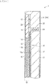
- FIG. 1 illustrates a cross-sectional configuration of an upper part and its surroundings of a display device (a display device 1) according to an embodiment of the invention.
- FIG. 2A illustrates, in perspective, an external appearance on front (display-surface) side of the display device 1.
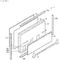
- FIG. 2B illustrates, in perspective and in an exploded manner, an overall configuration of the display device 1, as viewed from rear side.
- FIG. 3 illustrates a cross-sectional configuration of a lower part and its surroundings of the display device 1. It is to be noted that FIGs. 1 and 3 are cross-sectional views respectively taken along lines I-I and II-II illustrated in FIG. 2 . In FIG. 2B , the configuration is partially omitted.
- the display device 1 may be, for example, a liquid crystal display device used as a television device.
- the display device 1 may include optical members, besides a display panel 10.
- the optical members may include a reflection polarizing film 15, a light guide plate 16, a reflection sheet 17, an optical sheet 18, and a light source 19A.
- the light guide plate 16 may include a base having rigidity.
- an edge surface of the light guide plate 16 is attached to a frame 21 (a decorative member).
- chassis e.g., a middle chassis 131, a back chassis 132, and a rear cover 133 (refer to FIG. 5 )
- chassis e.g., a middle chassis 131, a back chassis 132, and a rear cover 133 (refer to FIG. 5 )
- the display device 1 may include a sealing member 13 provided in a periphery of the display panel 10.
- the sealing member 13 may include a front surface that is level with the front surface (the display surface) of the display panel 10 (specifically, a CF substrate 11B).
- a bonding film 14 may be bonded to the display surface of the display panel 10 including the sealing member 13.
- the display panel 10 may display an image such as a moving image or a still image.
- the display panel 10 may include, for example, a TFT (Thin Film Transistor) substrate 11A (a first substrate), the color filter (CF) substrate 11B (a second substrate), and a display layer (here, a liquid crystal layer 12) provided between the two substrates.
- the display panel 10 may include polarizing plates (not illustrated) provided on opposite surfaces to the liquid crystal layer 12 of the TFT substrate 11A and the CF substrate 11B (on the front surface (the display surface) and the rear surface of the display panel 10). The polarizing plates may each transmit polarized light in a specific direction.
- the TFT substrate 11A may include a glass substrate and a plurality of pixel electrodes (not illustrated) provided on the glass substrate.
- the plurality of pixel electrodes may be disposed, for example, in a matrix.
- the TFT substrate 11A may include TFT elements, gate lines and source lines, and other components (neither illustrated).
- the TFT elements may drive the plurality of respective pixel electrodes.
- the gate lines and the source lines may be coupled to the TFT elements.
- the pixel electrodes may be made of, for example, a conductive material having transparency, e.g., ITO (Indium Tin Oxide).
- the pixel electrodes may be provided on the glass substrate for respective subpixels (not illustrated).
- the TFT substrate 11A may be, for example, a rectangular substrate.
- one side of the TFT substrate 11A may be longer than a corresponding side of the CF substrate 11B, so as to form an extension.
- the extension of the TFT substrate 11A may include an electrode.
- One end of a printed circuit substrate 11C may be electrically coupled to the electrode through an anisotropic conductive film (ACF).
- ACF anisotropic conductive film
- the CF substrate 11B may include a glass substrate and a color filter (not illustrated) provided on the glass substrate.
- the color filter may include, for example, red (R), green (G), and blue (B) filters in stripes.
- the CF substrate 11B may also include an opposite electrode (not illustrated) over an entire surface of an effective display region on the color filter.
- the opposite electrode may be made of, for example, the conductive material having transparency, e.g., ITO, as with the pixel electrodes as mentioned above.
- a spacer may be provided between the opposite electrode and the pixel electrodes on side on which the TFT substrate 11A is disposed, although not illustrated here. The spacer may maintain a gap between both substrates.
- the printed circuit substrate 11C may have flexibility. As described above, the printed circuit substrate 11C may include the one end that is electrically coupled, through the ACF, to the electrode provided in the extension of the TFT substrate 11A. The printed circuit substrate 11C may include another end that is electrically coupled to a driver substrate 26A. The driver substrate 26A may be mounted on a back chassis 26 disposed on the rear side of the display panel 10.
- the liquid crystal layer 12 may include, for example, a liquid crystal material (liquid crystal molecules) having negative dielectric anisotropy, in a case of a normally black system.
- a liquid crystal material liquid crystal molecules
- the liquid crystal material having the negative dielectric anisotropy may include MLC-7026-000 (available from Merck KGaA).
- MLC-7026-000 available from Merck KGaA.
- the material used for the liquid crystal layer 12 is not limited thereto.
- IPS In Plane Switching
- a liquid crystal material having positive dielectric anisotropy may be used.
- the liquid crystal material having the positive dielectric anisotropy may be also used in a case of a normally white system such as a TN (Twisted Nematic) mode.
- the liquid crystal layer 12 may be sealed by a sealing material (not illustrated).
- the sealing material may be provided, in a periphery of the liquid crystal layer 12, between the TFT substrate 11A and the CF substrate 11B.
- alignment films may be provided between the liquid crystal layer 12 and the TFT substrate 11A, and between the liquid crystal layer 12 and the CF substrate 11B.
- the alignment films may cause the liquid crystal molecules to be adjusted in a predetermined alignment state.
- the alignment films either vertical alignment films or horizontal alignment films may be used.
- the sealing member 13 may be provided in the periphery of the display panel 10, as described above. This allows for planarization of a shouldered edge surface of the display panel 10 formed by combination of differently-sized members (i.e., the TFT substrate 11A and the CF substrate 11B).
- a general resin material may be used as the sealing member 13.
- a photocurable resin may be used.
- Specific examples may include an acrylic resin, an epoxy resin, and a silicone resin.
- one preferable example may be a resin having small shrinkage after curing.
- the silicon resin may be suitable.
- the sealing member 13 may be colored.
- coloring the sealing member 13 in black makes it possible to reduce light leakage through, for example, a side surface of the liquid crystal layer 12.
- Examples of a method of coloring the sealing member 13 may include adding a colorant, and using a resin material that changes color (is colored) by light irradiation in curing.
- the colorant may be a material that maintains transmittance of the sealing resin material. Examples may include carbon black and a metal-containing dye.
- the sealing member 13 may be provided in an entirety of the periphery of the display panel 10, but this is non-limiting.
- the sealing member 13 may be provided solely on one side of the rectangular-shaped display panel 10.
- the sealing member 13 may be provided in an interspaced manner on four sides of the display panel 10.
- the sealing member 13 may be provided in a pattern determined as necessary.
- the bonding film 14 may be bonded to the front surface (the display surface) of the display panel 10 including the sealing member 13.
- the bonding film 14 may protect the front surface of the display panel 10, and provide unity of the display panel 10 and the sealing member 13.
- the bonding film 14 may be a film having transparency over its entire surface, or alternatively, a film that is partly colored in black in a peripheral part of the display region.
- the reflection polarizing film 15 may transmit only polarized light or polarized wave in the specific direction, and cause reflection, toward the display panel 10, of light propagated through the light guide plate 16 from the light source 19A, without absorption of the light.
- the reflection polarizing film 15 may be attached to, for example, the TFT substrate 11A of the display panel 10, with an adhesive layer 15a in between.
- the light guide plate 16 may propagate light entering from the light source 19A to guide the light toward the display panel 10.
- the light guide plate 16 may have a planar shape of, for example, a rectangle.
- the light guide plate 16 may be made of a material having high transparency and having rigidity. In a more preferable example, a material having a small coefficient of thermal expansion may be used.
- the light guide plate 16 may include a glass base. Any adjustment may be made with respect to a shape, a size, a refractive index, a concentration, or distribution of the concentration, or other factors, so that desired characteristics are obtained.
- the reflection sheet 17 may prevent the light entering from the light source 19A from leaking through the light guide plate 16 to opposite side.
- the reflection sheet 17 may also cause efficient reflection, toward the display panel 10, of the light propagated through the light guide plate 16.
- the optical sheet 18 may be a sheet that provides various optical functions with respect to light that is emitted from the light source 19A to irradiate the display panel 10 through the light guide plate 16.
- the optical sheet 18 may include a single layer of a sheet, or a stack of sheets.
- the sheet or the sheets may have, for example, a function of dividing the light entering the display panel 10 from the light source 19A through the light guide plate 16 into the entering light and a polarized component orthogonal to the entering light, a function of compensating a phase difference of light waves to provide wide viewing angle or to prevent coloration, or a function of diffusing display light.
- a heatsink 19 is disposed on a rear surface of the reflection sheet 17, and include, for example, a bending surface that wraps around a lower surface (a bottom surface) of the light guide plate 16.
- the light source 19A may be disposed on the bending surface.
- a white LED Light Emitting Diode
- LEDs that provide red, green, and blue colors may be also used.
- a line light source such as a fluorescent lamp may be also used.
- the light source 19A may be disposed, for example, directly on one edge surface (the lower surface) of the light guide plate 16.
- the light source 19A may be disposed along four sides of the light guide plate 16.
- the display panel 10 may be disposed on a front surface of the display device 1.
- the frame 21 may be disposed.
- the frame 21 may serve as an exterior member of edge-surface parts of the display device 1, and fix the display panel 10 and the optical members as described above.
- the rear sheet 22 may be bonded on rear-surface side of the light guide plate 16, with the reflection sheet 17 in between.
- the rear sheet 22 may serve as an exterior.
- various kinds of metal plates 23A, 23B, and 23C, the back chassis 26 and a source shield 25, and other components may be attached near a lower part of the rear surface of the display device 1.
- the metal plates 23A, 23B, and 23C may serve as holding tools that allow for installation of the display device 1 on a stand or a wall, or other places.
- the back chassis 26 and the source shield 27 may be provided for mounting of the driver substrate 26A, and hold the driver substrate 26A. It is to be noted that these may be fixed in a stepped state to the light guide plate 16 so as to reduce contact area with the light guide plate 16, in order to prevent generation of stress due to a difference in the coefficients of thermal expansion between these and the light guide plate 16.
- the frame 21 may be divided into four parts, as illustrated in FIG. 2B , namely a frame 21A, a frame 21B, a frame 21C, and a frame 21D.
- the frame 21A may cover a top surface.
- the frames 21B and 21C may cover lateral side surfaces.
- the frame 21D may cover a bottom surface. These may be combined to constitute the frame 21 in a frame shape.
- the frame 21 may be made of, for example, a metal having high thermal conductivity. Specific and preferable examples may include aluminum (Al) in terms of costs and small weight. Besides, other materials may be also used, examples of which may include iron (Fe), polycarbonate (PC), and plastic in which an ABS resin is added to PC.
- the display panel 10 may be attached to the frame 21, with an adhesive layer 23.
- the adhesive layer 23 may be provided on a rear surface of the sealing member 13 provided in the periphery of the display panel 10.
- the adhesive layer 23 may be made of a soft resin material, in order to reduce stress applied to the display panel 10.
- a resin material of a closed-cell foam may be used. Using such a material makes it possible to absorb a difference in expansion and shrinkage of parts due to heat, and to prevent generation of display unevenness.
- the light guide plate 16 may be attached to the frame 21, with an adhesive layer 24 provided on edge surfaces of the light guide plate 16.
- an UV resin material may be used as the adhesive layer 24.
- the optical sheet 18 may not be bonded to the light guide plate 16. Instead, a part of the optical sheet may be disposed in a suspended state along the edge surface of the light guide plate 16.
- FIG. 4A schematically illustrates the suspended part and its surroundings of the optical sheet 18 along the light guide plate 16.
- FIG. 4B illustrates, in perspective, a shape of the surroundings of the suspended part of the optical sheet 18.
- the optical sheet 18 may include a lug (a tab 18A) as illustrated in FIG. 4B , at a predetermined position.
- the tab 18A may be turned out toward the light guide plate 16, and have a suspension hole 18B that extends across the turned-out part.
- the optical sheet 18 may be suspended by hooking the turned-out tab 18A over the edge surface of the light guide plate 16, and inserting a stopper 28 in the suspension hole 18B. In this way, it is possible to prevent the optical sheet 18 from being twisted due to the difference in the coefficients of thermal expansion between the light guide plate 16 and the optical sheet 18.
- the adhesive layer 24 may include a dam material 29 at a position outward of the suspended part.
- the dam material 29 may prevent an adhesive from flowing into the suspended part and its surroundings, in order to prevent the optical sheet 18 from unintentionally being attached to the light guide plate 16 when light guide plate 16 is attached to the frame 21 with the adhesive layer 24. It is to be noted that the description here is given of an example of installation of the optical sheet 18 solely on a top side of the light guide plate 16, but this is non-limiting.
- the lug as described above may be provided on all four sides of the optical sheet 16, so as to install the optical sheet 18 on all sides of the light guide plate 16.
- the rear sheet 22 may keep external light from entering an inside of the display device 1, and adjust an external appearance of the rear surface of the display device 1.
- the rear sheet 22 may be made of, for example, a black-colored metal sheet such as aluminum (Al), and a resin film such as a black film that is mixed with a black colorant and has optical density of 1 or more.
- a metal having high thermal conductivity specifically aluminum (Al)
- Al aluminum
- iron (Fe), polycarbonate (PC), or plastic with an ABS resin added thereto may be also used. It is to be noted that the use of the metal material makes it possible to shield an electromagnetic wave generated from various circuits and electronic components. This leads to reduction in unwanted radiation generated from various circuits and electronic components provided in the inside of the display device 1.
- the display device 1 may provide picture display by application of a drive voltage between the TFT substrate 11A and the CF substrate 11B.
- the application of the drive voltage may cause a change in the alignment state of the liquid crystal molecules included in the liquid crystal layer 12, in response to an electric potential difference between the TFT substrate 11A and the CF substrate 11B.
- the liquid crystal molecules may make a response so as to change their attitude from vertical inclination (at a right angle) to horizontal inclination (in parallel) with respect to the TFT substrate 11A and the CF substrate 11B.
- the liquid crystal molecules may make a response so as to change their attitude from the horizontal inclination (in parallel) to the vertical inclination (at the right angle) with respect to the TFT substrate 11A and the CF substrate 11B.
- the change in optical characteristics of the liquid crystal layer 12 may cause entering light to be modulated by the liquid crystal molecules to become emission light.
- the entering light refers to light emitted from the light source 19A and entering the liquid crystal layer 12 through the light guide plate 16.
- Gradation expression may be made on the basis of the emission light, to provide the picture display.
- FIG. 5 illustrates a cross-sectional configuration near a top surface of a general display device 100.
- a light guide plate 116 may be made of, for example, a resin material such as an acrylic resin.
- the light guide plate 116 made of, for example, an acrylic resin has small rigidity.
- optical members such as the light guide plate 116, a reflection sheet 117, and an optical sheet 118 may be held by holder members such as the middle chassis 131 and the back chassis 132.
- the optical members and a display panel 110, and other components may be held by, for example, the middle chassis 131 and the back chassis 132, and may be accommodated in a casing.
- the casing may include a frame 121 and a rear cover 133 that cover a peripheral region (a frame border part) of the display panel 110 and side surfaces of the display panel and the optical members. It is to be noted that the display panel 110, the frame 121, the back chassis 132, and the rear cover 133 may each be fixed by screwing.
- the holder members may hold the display panel 110 and the optical members, and include, for example, the middle chassis 131 and the back chassis 132.
- the casing may accommodate them. Accordingly, it is difficult to reduce a thickness of the display device.
- fixing the holder members and the casing with, for example, screws results in the large number of components, and large weight due to weight of the components.
- the light guide plate 16 may include the base having rigidity.
- the edge surface of the light guide plate 16 is attached and fixed to the frame 21. Accordingly, the reflection sheet 17 and the optical sheet 18 are held by the light guide plate 16.
- This allows for omission of the middle chassis 131, and simplification of the back chassis 132 so that the back chassis 132 is provided solely in a necessary part (here, a lower part of the rear surface on which the driver substrate 26A is mounted).
- attaching the rear sheet 22 to the rear surface of the light guide plate 16 allows for elimination of the rear cover 133.
- the light guide plate 16 may include the base having rigidity.
- the edge surface of the light guide plate 16 is attached to the frame 21.
- This allows for elimination of the holder members such as the middle chassis 131 and the back chassis 132, and the rear member such as the rear cover 133.
- it is possible to significantly reduce the number of components and to reduce weight in association therewith.
- it is possible to provide the low-profile display device 1. In other words, it is possible to provide a higher degree of freedom in design of the display device 1, and enhance desinability of the external appearance of the display device 1.
- the display panel 10 may be fixed to the frame 21, with the adhesive layer 23 in between, on the rear surface of the sealing member 13 provided in the periphery of the display panel 10.
- This allows for elimination, from the frame 21, of a frame border part that covers the periphery of the display panel 10.
- the display device 1 is exemplified by the liquid crystal display device.
- the technology may be also applicable to a plasma display device or an organic electroluminescence display device.
Landscapes
- Physics & Mathematics (AREA)
- Nonlinear Science (AREA)
- General Physics & Mathematics (AREA)
- Optics & Photonics (AREA)
- Mathematical Physics (AREA)
- Chemical & Material Sciences (AREA)
- Crystallography & Structural Chemistry (AREA)
- Liquid Crystal (AREA)
- Engineering & Computer Science (AREA)
- Theoretical Computer Science (AREA)
- Devices For Indicating Variable Information By Combining Individual Elements (AREA)
Description
- The disclosure relates to a display device such as a television device.
- In a display device typified by, for example, a liquid crystal display device, an organic EL display device, and an electrophoretic display device, there has been pursuit of a display device having a lower profile and a smaller weight. In a general display device, a display panel may be accommodated in a casing. The casing may include a front casing and a rear casing. The front casing may be disposed on display-surface side of the display panel, and include, for example, a front bezel and a top chassis. The rear casing may cover rear-surface side of the display panel, and include, for example, a back chassis, a frame, and a rear cover. (For example, reference is made to PTL 1.) PTL 2 discloses a thin image display device which is free from display defects caused by the deformation of an image display unit and has no unnecessary resin adhering to a backlight side. PTL 3 discloses a method for manufacturing an image display device includes the step of forming a cured resin layer by interposing a photo-curable resin composition between a base including an image display unit such as a liquid crystal display panel and a light-transmitting protection member including a light-shielding member and then photo-curing the photo-curable resin composition. PTL 3 discloses a liquid crystal display having a liquid crystal panel having a liquid crystal layer sandwiched by a pair of substrates, and a backlight unit, wherein a reflective polarizer of specific properties is arranged between a first substrate and the backlight unit.. PTL 4 discloses an electrooptical device including an electrooptical panel, a light guide plate disposed so as to be opposed to one panel surface of the electrooptical panel and a frame holding the electrooptical panel and the light guide plate and including a metal frame member.
-
- [PTL 1]
Japanese Unexamined Patent Application Publication No. 2008-304630 - [PTL 2]
EP 2 144 218 A1 - [PTL 3]
EP 2 133 855 A1 - [PTL 4]
US 2007/0058110 A1 - [PTL 5]
JP 2010 217524 A -
WO2014/051924 discloses a display device having a closed-cell foam provided between an outer frame and the cover glass to reduce the effects of thermal expansion in combination with a heat sink located in contact with the light guide of the backlight. - In recent years, in the display device such as the liquid crystal display device, advance in techniques of the display panel and electronic components has brought enhancement in designability of an external appearance. For purpose of further enhancement, there has been pursuit of the lower profile and a narrower frame border of the display device. However, in an existing display device, as disclosed in PTL 1 mentioned above, the casing that accommodates a liquid crystal panel may include a plurality of members. This constitutes hindrance to the enhancement in the designability such as the lower profile.
- It is therefore desirable to provide a display device that makes it possible to reduce the number of components and to enhance designability.
- A display device according to an embodiment of the invention is set out in the appended set of claims.
-
- [
FIG. 1] FIG. 1 is a cross-sectional view of an upper part and its surroundings of a display device according to an embodiment of the invention. - [
FIG. 2A] FIG. 2A is a perspective view of an external appearance on front side of the display device illustrated inFIG. 1 . - [
FIG. 2B] FIG. 2B is an exploded perspective view of the display device illustrated inFIG. 2 , as viewed from rear. - [
FIG. 3] FIG. 3 is a cross-sectional view of a lower part and its surroundings of the display device illustrated inFIG. 2 . - [
FIG 4A] FIG. 4A schematically illustrates an attachment part and its surroundings where a light guide plate of the display device illustrated inFIG. 2 is attached to a frame. - [
FIG. 4B] FIG. 4B is a perspective view of an optical sheet illustrated inFIG. 4 . - [
FIG. 5] FIG. 5 is a cross-sectional view of an upper part of a general display device. - Some embodiments of the invention are described in detail with reference to the drawings, in the following order.
- 1. Embodiment (an example in which a light guide plate is made of a material having rigidity, and an edge surface thereof is attached to a frame)
- 1.1 Overall Configuration
- 1.2 Description of Parts
- 1.3 Workings and Effects
-
FIG. 1 illustrates a cross-sectional configuration of an upper part and its surroundings of a display device (a display device 1) according to an embodiment of the invention.FIG. 2A illustrates, in perspective, an external appearance on front (display-surface) side of the display device 1.FIG. 2B illustrates, in perspective and in an exploded manner, an overall configuration of the display device 1, as viewed from rear side.FIG. 3 illustrates a cross-sectional configuration of a lower part and its surroundings of the display device 1. It is to be noted thatFIGs. 1 and3 are cross-sectional views respectively taken along lines I-I and II-II illustrated inFIG. 2 . InFIG. 2B , the configuration is partially omitted. The display device 1 may be, for example, a liquid crystal display device used as a television device. - The display device 1 may include optical members, besides a
display panel 10. Examples of the optical members may include areflection polarizing film 15, alight guide plate 16, areflection sheet 17, anoptical sheet 18, and alight source 19A. In this embodiment, thelight guide plate 16 may include a base having rigidity. Moreover, an edge surface of thelight guide plate 16 is attached to a frame 21 (a decorative member). Hence, it is possible to eliminate or simplify chassis (e.g., amiddle chassis 131, aback chassis 132, and a rear cover 133 (refer toFIG. 5 )) that may be used as holder members in a general display device. - The display device 1 may include a sealing
member 13 provided in a periphery of thedisplay panel 10. The sealingmember 13 may include a front surface that is level with the front surface (the display surface) of the display panel 10 (specifically, aCF substrate 11B). Abonding film 14 may be bonded to the display surface of thedisplay panel 10 including the sealingmember 13. - The
display panel 10 may display an image such as a moving image or a still image. Thedisplay panel 10 may include, for example, a TFT (Thin Film Transistor)substrate 11A (a first substrate), the color filter (CF)substrate 11B (a second substrate), and a display layer (here, a liquid crystal layer 12) provided between the two substrates. Thedisplay panel 10 may include polarizing plates (not illustrated) provided on opposite surfaces to theliquid crystal layer 12 of theTFT substrate 11A and theCF substrate 11B (on the front surface (the display surface) and the rear surface of the display panel 10). The polarizing plates may each transmit polarized light in a specific direction. - The
TFT substrate 11A may include a glass substrate and a plurality of pixel electrodes (not illustrated) provided on the glass substrate. The plurality of pixel electrodes may be disposed, for example, in a matrix. TheTFT substrate 11A may include TFT elements, gate lines and source lines, and other components (neither illustrated). The TFT elements may drive the plurality of respective pixel electrodes. The gate lines and the source lines may be coupled to the TFT elements. The pixel electrodes may be made of, for example, a conductive material having transparency, e.g., ITO (Indium Tin Oxide). The pixel electrodes may be provided on the glass substrate for respective subpixels (not illustrated). - The
TFT substrate 11A may be, for example, a rectangular substrate. Here, although illustrated in a simplified manner, one side of theTFT substrate 11A may be longer than a corresponding side of theCF substrate 11B, so as to form an extension. The extension of theTFT substrate 11A may include an electrode. One end of a printed circuit substrate 11C may be electrically coupled to the electrode through an anisotropic conductive film (ACF). - The
CF substrate 11B may include a glass substrate and a color filter (not illustrated) provided on the glass substrate. The color filter may include, for example, red (R), green (G), and blue (B) filters in stripes. TheCF substrate 11B may also include an opposite electrode (not illustrated) over an entire surface of an effective display region on the color filter. The opposite electrode may be made of, for example, the conductive material having transparency, e.g., ITO, as with the pixel electrodes as mentioned above. It is to be noted a spacer may be provided between the opposite electrode and the pixel electrodes on side on which theTFT substrate 11A is disposed, although not illustrated here. The spacer may maintain a gap between both substrates. - The printed circuit substrate 11C may have flexibility. As described above, the printed circuit substrate 11C may include the one end that is electrically coupled, through the ACF, to the electrode provided in the extension of the
TFT substrate 11A. The printed circuit substrate 11C may include another end that is electrically coupled to adriver substrate 26A. Thedriver substrate 26A may be mounted on aback chassis 26 disposed on the rear side of thedisplay panel 10. - The
liquid crystal layer 12 may include, for example, a liquid crystal material (liquid crystal molecules) having negative dielectric anisotropy, in a case of a normally black system. Examples of the liquid crystal material having the negative dielectric anisotropy may include MLC-7026-000 (available from Merck KGaA). It is to be noted that the material used for theliquid crystal layer 12 is not limited thereto. For example, in a case of an IPS (In Plane Switching) mode, a liquid crystal material having positive dielectric anisotropy may be used. Moreover, the liquid crystal material having the positive dielectric anisotropy may be also used in a case of a normally white system such as a TN (Twisted Nematic) mode. It is to be noted that theliquid crystal layer 12 may be sealed by a sealing material (not illustrated). The sealing material may be provided, in a periphery of theliquid crystal layer 12, between theTFT substrate 11A and theCF substrate 11B. Moreover, alignment films (not illustrated) may be provided between theliquid crystal layer 12 and theTFT substrate 11A, and between theliquid crystal layer 12 and theCF substrate 11B. The alignment films may cause the liquid crystal molecules to be adjusted in a predetermined alignment state. As the alignment films, either vertical alignment films or horizontal alignment films may be used. - The sealing
member 13 may be provided in the periphery of thedisplay panel 10, as described above. This allows for planarization of a shouldered edge surface of thedisplay panel 10 formed by combination of differently-sized members (i.e., theTFT substrate 11A and theCF substrate 11B). - For example, a general resin material may be used as the sealing
member 13. In particular, in one preferable example, a photocurable resin may be used. Specific examples may include an acrylic resin, an epoxy resin, and a silicone resin. Among these, one preferable example may be a resin having small shrinkage after curing. In particular, the silicon resin may be suitable. The sealingmember 13 may be colored. For example, coloring the sealingmember 13 in black makes it possible to reduce light leakage through, for example, a side surface of theliquid crystal layer 12. Examples of a method of coloring the sealingmember 13 may include adding a colorant, and using a resin material that changes color (is colored) by light irradiation in curing. In one preferable example, the colorant may be a material that maintains transmittance of the sealing resin material. Examples may include carbon black and a metal-containing dye. - It is to be noted that the sealing
member 13 may be provided in an entirety of the periphery of thedisplay panel 10, but this is non-limiting. For example, the sealingmember 13 may be provided solely on one side of the rectangular-shapeddisplay panel 10. In another alternative, the sealingmember 13 may be provided in an interspaced manner on four sides of thedisplay panel 10. The sealingmember 13 may be provided in a pattern determined as necessary. - The
bonding film 14 may be bonded to the front surface (the display surface) of thedisplay panel 10 including the sealingmember 13. Thebonding film 14 may protect the front surface of thedisplay panel 10, and provide unity of thedisplay panel 10 and the sealingmember 13. Thebonding film 14 may be a film having transparency over its entire surface, or alternatively, a film that is partly colored in black in a peripheral part of the display region. - The
reflection polarizing film 15 may transmit only polarized light or polarized wave in the specific direction, and cause reflection, toward thedisplay panel 10, of light propagated through thelight guide plate 16 from thelight source 19A, without absorption of the light. Thereflection polarizing film 15 may be attached to, for example, theTFT substrate 11A of thedisplay panel 10, with anadhesive layer 15a in between. - The
light guide plate 16 may propagate light entering from thelight source 19A to guide the light toward thedisplay panel 10. Thelight guide plate 16 may have a planar shape of, for example, a rectangle. In this embodiment, in one preferable example, thelight guide plate 16 may be made of a material having high transparency and having rigidity. In a more preferable example, a material having a small coefficient of thermal expansion may be used. In one specific and preferable example, thelight guide plate 16 may include a glass base. Any adjustment may be made with respect to a shape, a size, a refractive index, a concentration, or distribution of the concentration, or other factors, so that desired characteristics are obtained. - The
reflection sheet 17 may prevent the light entering from thelight source 19A from leaking through thelight guide plate 16 to opposite side. Thereflection sheet 17 may also cause efficient reflection, toward thedisplay panel 10, of the light propagated through thelight guide plate 16. - The
optical sheet 18 may be a sheet that provides various optical functions with respect to light that is emitted from thelight source 19A to irradiate thedisplay panel 10 through thelight guide plate 16. Theoptical sheet 18 may include a single layer of a sheet, or a stack of sheets. The sheet or the sheets may have, for example, a function of dividing the light entering thedisplay panel 10 from thelight source 19A through thelight guide plate 16 into the entering light and a polarized component orthogonal to the entering light, a function of compensating a phase difference of light waves to provide wide viewing angle or to prevent coloration, or a function of diffusing display light. - A
heatsink 19 is disposed on a rear surface of thereflection sheet 17, and include, for example, a bending surface that wraps around a lower surface (a bottom surface) of thelight guide plate 16. Thelight source 19A may be disposed on the bending surface. As thelight source 19A, for example, a white LED (Light Emitting Diode) may be used. Alternatively, LEDs that provide red, green, and blue colors may be also used. Moreover, besides a point light source such as an LED, a line light source such as a fluorescent lamp may be also used. Thelight source 19A may be disposed, for example, directly on one edge surface (the lower surface) of thelight guide plate 16. Alternatively, thelight source 19A may be disposed along four sides of thelight guide plate 16. - The parts that constitute the display device 1 as described above may be assembled as follows. In the display device 1, referring to
FIGs. 2A and2B , thedisplay panel 10 may be disposed on a front surface of the display device 1. On side surfaces of thedisplay panel 10, theframe 21 may be disposed. Theframe 21 may serve as an exterior member of edge-surface parts of the display device 1, and fix thedisplay panel 10 and the optical members as described above. On a rear surface of the display device 1, therear sheet 22 may be bonded on rear-surface side of thelight guide plate 16, with thereflection sheet 17 in between. Therear sheet 22 may serve as an exterior. Further, various kinds of metal plates 23A, 23B, and 23C, theback chassis 26 and a source shield 25, and other components may be attached near a lower part of the rear surface of the display device 1. The metal plates 23A, 23B, and 23C may serve as holding tools that allow for installation of the display device 1 on a stand or a wall, or other places. Theback chassis 26 and thesource shield 27 may be provided for mounting of thedriver substrate 26A, and hold thedriver substrate 26A. It is to be noted that these may be fixed in a stepped state to thelight guide plate 16 so as to reduce contact area with thelight guide plate 16, in order to prevent generation of stress due to a difference in the coefficients of thermal expansion between these and thelight guide plate 16. - The
frame 21 may be divided into four parts, as illustrated inFIG. 2B , namely aframe 21A, aframe 21B, a frame 21C, and aframe 21D. Theframe 21A may cover a top surface. Theframes 21B and 21C may cover lateral side surfaces. Theframe 21D may cover a bottom surface. These may be combined to constitute theframe 21 in a frame shape. In one preferable example, theframe 21 may be made of, for example, a metal having high thermal conductivity. Specific and preferable examples may include aluminum (Al) in terms of costs and small weight. Besides, other materials may be also used, examples of which may include iron (Fe), polycarbonate (PC), and plastic in which an ABS resin is added to PC. - The
display panel 10 may be attached to theframe 21, with anadhesive layer 23. Theadhesive layer 23 may be provided on a rear surface of the sealingmember 13 provided in the periphery of thedisplay panel 10. In one preferable example, theadhesive layer 23 may be made of a soft resin material, in order to reduce stress applied to thedisplay panel 10. For example, in one preferable example, a resin material of a closed-cell foam may be used. Using such a material makes it possible to absorb a difference in expansion and shrinkage of parts due to heat, and to prevent generation of display unevenness. - Moreover, the
light guide plate 16 may be attached to theframe 21, with anadhesive layer 24 provided on edge surfaces of thelight guide plate 16. In one preferable example, an UV resin material may be used as theadhesive layer 24. In this embodiment, referring toFIG. 4A , thelight guide plate 16 and theframe 21 may be attached in an interspaced state by theadhesive layer 24. In the display device 1, theoptical sheet 18 may not be bonded to thelight guide plate 16. Instead, a part of the optical sheet may be disposed in a suspended state along the edge surface of thelight guide plate 16.FIG. 4A schematically illustrates the suspended part and its surroundings of theoptical sheet 18 along thelight guide plate 16.FIG. 4B illustrates, in perspective, a shape of the surroundings of the suspended part of theoptical sheet 18. Theoptical sheet 18 may include a lug (atab 18A) as illustrated inFIG. 4B , at a predetermined position. Thetab 18A may be turned out toward thelight guide plate 16, and have asuspension hole 18B that extends across the turned-out part. Theoptical sheet 18 may be suspended by hooking the turned-outtab 18A over the edge surface of thelight guide plate 16, and inserting astopper 28 in thesuspension hole 18B. In this way, it is possible to prevent theoptical sheet 18 from being twisted due to the difference in the coefficients of thermal expansion between thelight guide plate 16 and theoptical sheet 18. Moreover, theadhesive layer 24 may include adam material 29 at a position outward of the suspended part. Thedam material 29 may prevent an adhesive from flowing into the suspended part and its surroundings, in order to prevent theoptical sheet 18 from unintentionally being attached to thelight guide plate 16 whenlight guide plate 16 is attached to theframe 21 with theadhesive layer 24. It is to be noted that the description here is given of an example of installation of theoptical sheet 18 solely on a top side of thelight guide plate 16, but this is non-limiting. For example, the lug as described above may be provided on all four sides of theoptical sheet 16, so as to install theoptical sheet 18 on all sides of thelight guide plate 16. - The
rear sheet 22 may keep external light from entering an inside of the display device 1, and adjust an external appearance of the rear surface of the display device 1. Therear sheet 22 may be made of, for example, a black-colored metal sheet such as aluminum (Al), and a resin film such as a black film that is mixed with a black colorant and has optical density of 1 or more. - As the
back chassis 26 and thesource shield 27, for example, a metal having high thermal conductivity, specifically aluminum (Al), may be used. In addition, iron (Fe), polycarbonate (PC), or plastic with an ABS resin added thereto may be also used. It is to be noted that the use of the metal material makes it possible to shield an electromagnetic wave generated from various circuits and electronic components. This leads to reduction in unwanted radiation generated from various circuits and electronic components provided in the inside of the display device 1. - The display device 1 may provide picture display by application of a drive voltage between the
TFT substrate 11A and theCF substrate 11B. In one specific example, the application of the drive voltage may cause a change in the alignment state of the liquid crystal molecules included in theliquid crystal layer 12, in response to an electric potential difference between theTFT substrate 11A and theCF substrate 11B. Regarding the alignment state of the liquid crystal molecules, in a case with use of the vertical alignment films in the normally black system, the liquid crystal molecules may make a response so as to change their attitude from vertical inclination (at a right angle) to horizontal inclination (in parallel) with respect to theTFT substrate 11A and theCF substrate 11B. In contrast, in the normally white system such as the TN mode, the liquid crystal molecules may make a response so as to change their attitude from the horizontal inclination (in parallel) to the vertical inclination (at the right angle) with respect to theTFT substrate 11A and theCF substrate 11B. In this way, the change in optical characteristics of theliquid crystal layer 12 may cause entering light to be modulated by the liquid crystal molecules to become emission light. The entering light refers to light emitted from thelight source 19A and entering theliquid crystal layer 12 through thelight guide plate 16. Gradation expression may be made on the basis of the emission light, to provide the picture display. -
FIG. 5 illustrates a cross-sectional configuration near a top surface of ageneral display device 100. In thedisplay device 100, alight guide plate 116 may be made of, for example, a resin material such as an acrylic resin. Thelight guide plate 116 made of, for example, an acrylic resin has small rigidity. Accordingly, optical members such as thelight guide plate 116, areflection sheet 117, and anoptical sheet 118 may be held by holder members such as themiddle chassis 131 and theback chassis 132. In one configuration example, the optical members and adisplay panel 110, and other components may be held by, for example, themiddle chassis 131 and theback chassis 132, and may be accommodated in a casing. The casing may include aframe 121 and arear cover 133 that cover a peripheral region (a frame border part) of thedisplay panel 110 and side surfaces of the display panel and the optical members. It is to be noted that thedisplay panel 110, theframe 121, theback chassis 132, and therear cover 133 may each be fixed by screwing. - Thus, in the
general display device 100, it is necessary to provide the holder members and the casing. The holder members may hold thedisplay panel 110 and the optical members, and include, for example, themiddle chassis 131 and theback chassis 132. The casing may accommodate them. Accordingly, it is difficult to reduce a thickness of the display device. Moreover, fixing the holder members and the casing with, for example, screws results in the large number of components, and large weight due to weight of the components. - In contrast, in the display device 1 of this embodiment, the
light guide plate 16 may include the base having rigidity. The edge surface of thelight guide plate 16 is attached and fixed to theframe 21. Accordingly, thereflection sheet 17 and theoptical sheet 18 are held by thelight guide plate 16. This allows for omission of themiddle chassis 131, and simplification of theback chassis 132 so that theback chassis 132 is provided solely in a necessary part (here, a lower part of the rear surface on which thedriver substrate 26A is mounted). Moreover, attaching therear sheet 22 to the rear surface of thelight guide plate 16 allows for elimination of therear cover 133. - As described, in this embodiment, the
light guide plate 16 may include the base having rigidity. The edge surface of thelight guide plate 16 is attached to theframe 21. This allows for elimination of the holder members such as themiddle chassis 131 and theback chassis 132, and the rear member such as therear cover 133. Hence, it is possible to significantly reduce the number of components and to reduce weight in association therewith. Moreover, it is possible to provide the low-profile display device 1. In other words, it is possible to provide a higher degree of freedom in design of the display device 1, and enhance desinability of the external appearance of the display device 1. - Furthermore, in this embodiment, the
display panel 10 may be fixed to theframe 21, with theadhesive layer 23 in between, on the rear surface of the sealingmember 13 provided in the periphery of thedisplay panel 10. This allows for elimination, from theframe 21, of a frame border part that covers the periphery of thedisplay panel 10. In other words, it is possible to eliminate an overlap region in which a frame border part of thedisplay panel 10 overlaps the frame border part of theframe 21. This leads to reduction in a frame border region. - Although description has been made by giving the embodiment as mentioned above, the contents of the technology are not limited to the above-mentioned example embodiments and may be modified in a variety of ways. For example, in the forgoing embodiment, the display device 1 is exemplified by the liquid crystal display device. However, the technology may be also applicable to a plasma display device or an organic electroluminescence display device.
Claims (15)
- A display device (1), comprising:a display panel (10);a sealing member (13) provided in the periphery of the display panel (10);a frame (21) that holds the display panel;a light guide plate (16) that has rigidity and includes an edge surface attached to the frame (21);a reflection sheet (17) adapted to prevent the light entering from a light source (19A) from leaking through the light guide plate (16) to an opposite side; anda heatsink (19) disposed on a rear surface of the reflection sheet (17), wherein the sealing member (13) is attached to the frame (21) with an adhesive layer (23) which is made of a closed-cell foam.
- The display device (1) according to claim 1, wherein the light guide plate (16) is attached to the frame (21), with an adhesive layer (24) in between.
- The display device (1) according to claim 1, wherein the light guide plate (16) includes a glass base.
- The display device (1) according to claim 1, the sealing member (13) including a surface that is level with a display surface of the display panel (10).
- The display device (1) according to claim 4, further comprising a bonding film (14) bonded to a front surface of the display panel (10) and a front surface of the sealing member (13).
- The display device (1) according to claim 1, further comprising a rear sheet (22) disposed on a rear surface of the light guide plate (16).
- The display device (1) according to any of the preceding claims, further comprising a reflection polarizing film (15), whereinthe display panel (10) includes a first substrate, a display layer, and a second substrate that are stacked in order, andthe reflection polarizing film (15) is disposed on an opposite surface to the display layer of the first substrate.
- The display device according to any of the preceding claims, wherein a light source (19A) is disposed on at least one side of the light guide plate.
- The display device according to claim 8, the light source (19A) comprises LEDs.
- The display device according to claim 9, the LEDs comprise red, green and blue LEDs.
- The display device according to claim 1, wherein the heat sink has a bent surface that extends around a portion of a lower surface of the light guide plate.
- The display device according to claim 11, further comprising a light source disposed on a first portion of the bent surface of the heat sink.
- The display device according to claim 12, wherein the bent surface of the heat sink comprises a cornered surface having a second portion extending in a different direction than the first portion and along a lengthwise direction of the light guide plate.
- The display device according to claim 1, further comprising an optical sheet (18) having a first member and a second member (18A), the first member disposed directly on a first surface of the light guide plate that extends in a lengthwise direction of the light guide plate and the second member disposed directly on a second surface of the light plate that extends in a depthwise direction of the light guide plate so as to form a lug (18A), the lug having an opening (18B) operable to dispose the optical sheet in the suspended state.
- The display device according to claim 14, wherein the optical sheet is provided on a display-surface side with respect to the light guide plate
Applications Claiming Priority (2)
| Application Number | Priority Date | Filing Date | Title |
|---|---|---|---|
| JP2014174200 | 2014-08-28 | ||
| PCT/JP2015/069441 WO2016031394A1 (en) | 2014-08-28 | 2015-07-06 | Display device |
Publications (3)
| Publication Number | Publication Date |
|---|---|
| EP3188163A1 EP3188163A1 (en) | 2017-07-05 |
| EP3188163A4 EP3188163A4 (en) | 2018-07-18 |
| EP3188163B1 true EP3188163B1 (en) | 2022-04-06 |
Family
ID=55399298
Family Applications (1)
| Application Number | Title | Priority Date | Filing Date |
|---|---|---|---|
| EP15835522.2A Active EP3188163B1 (en) | 2014-08-28 | 2015-07-06 | Display device |
Country Status (5)
| Country | Link |
|---|---|
| US (1) | US10816837B2 (en) |
| EP (1) | EP3188163B1 (en) |
| JP (1) | JP6601398B2 (en) |
| CN (2) | CN113643618B (en) |
| WO (1) | WO2016031394A1 (en) |
Families Citing this family (11)
| Publication number | Priority date | Publication date | Assignee | Title |
|---|---|---|---|---|
| JP7085472B2 (en) * | 2016-05-25 | 2022-06-16 | ソニーグループ株式会社 | Light emitting unit, liquid crystal module, display device and lighting device |
| CN107621665B (en) * | 2016-07-13 | 2020-09-22 | 群创光电股份有限公司 | display screen |
| CN107765477B (en) * | 2016-08-23 | 2023-10-13 | 京东方科技集团股份有限公司 | Film materials, backlight modules and display devices |
| KR20190014292A (en) * | 2017-08-01 | 2019-02-12 | 삼성디스플레이 주식회사 | Optical member, Backlight Unit including the same and method for Backlight Unit |
| USD848528S1 (en) * | 2017-09-08 | 2019-05-14 | Samsung Electronics Co., Ltd. | Digital signage |
| USD848529S1 (en) * | 2017-09-08 | 2019-05-14 | Samsung Electronics Co., Ltd. | Digital signage |
| KR102544326B1 (en) * | 2018-08-27 | 2023-06-19 | 삼성디스플레이 주식회사 | Display device |
| US10908459B2 (en) * | 2018-11-07 | 2021-02-02 | Sharp Kabushiki Kaisha | Lighting device and display device |
| US11003208B2 (en) | 2018-12-18 | 2021-05-11 | Apple Inc. | Display having optical films with bent alignment structures |
| JP6823278B1 (en) * | 2020-09-04 | 2021-02-03 | 富士通クライアントコンピューティング株式会社 | Display device |
| JP7691275B2 (en) * | 2021-05-06 | 2025-06-11 | シャープ株式会社 | Display Module |
Citations (1)
| Publication number | Priority date | Publication date | Assignee | Title |
|---|---|---|---|---|
| WO2014051924A1 (en) * | 2012-09-26 | 2014-04-03 | Apple Inc. | Computer backlight unit (blu) attachment to cover glass/cell |
Family Cites Families (61)
| Publication number | Priority date | Publication date | Assignee | Title |
|---|---|---|---|---|
| JPH03243985A (en) | 1990-06-15 | 1991-10-30 | Hitachi Ltd | Liquid crystal display unit and liquid crystal display device |
| JPH1184351A (en) * | 1997-09-11 | 1999-03-26 | Toshiba Corp | Liquid crystal display |
| JP2002196312A (en) * | 2000-12-25 | 2002-07-12 | Hitachi Ltd | Liquid crystal display |
| CN100409076C (en) * | 2003-07-16 | 2008-08-06 | 夏普株式会社 | Liquid crystal display device and backlight device |
| JP2006011242A (en) | 2004-06-29 | 2006-01-12 | Kyocera Corp | Liquid crystal display |
| KR101189088B1 (en) * | 2005-06-22 | 2012-11-09 | 삼성디스플레이 주식회사 | Back light assembly and liquid crystal display apparatus having the same |
| JP4602878B2 (en) | 2005-09-14 | 2010-12-22 | 株式会社 日立ディスプレイズ | Liquid crystal display |
| TWI348571B (en) * | 2005-12-15 | 2011-09-11 | Tpo Hong Kong Holding Ltd | Display module |
| JP2007240649A (en) * | 2006-03-06 | 2007-09-20 | Sony Corp | Optical display device |
| JP4883523B2 (en) | 2006-03-22 | 2012-02-22 | Nltテクノロジー株式会社 | Liquid crystal display |
| CN100529911C (en) * | 2006-06-30 | 2009-08-19 | 索尼株式会社 | Backlight device, liquid crystal display device and electric equipment |
| KR101527980B1 (en) * | 2007-04-03 | 2015-06-10 | 데쿠세리아루즈 가부시키가이샤 | Manufacturing method of image display device |
| JP5401824B2 (en) | 2007-04-09 | 2014-01-29 | デクセリアルズ株式会社 | Image display device |
| JP4552155B2 (en) * | 2007-04-27 | 2010-09-29 | ソニー株式会社 | Television equipment |
| WO2008143418A1 (en) * | 2007-05-23 | 2008-11-27 | Lg Innotek Co., Ltd. | Display device |
| JP2008305576A (en) * | 2007-06-05 | 2008-12-18 | Toshiba Matsushita Display Technology Co Ltd | Illumination unit and liquid crystal display device including the same |
| JP2008304630A (en) | 2007-06-06 | 2008-12-18 | Hitachi Ltd | Liquid crystal display |
| JP4575486B2 (en) * | 2007-10-24 | 2010-11-04 | セイコーインスツル株式会社 | Display device |
| CN101435948B (en) * | 2007-11-14 | 2012-12-26 | 奇美电子股份有限公司 | Backlight module and liquid crystal display including same |
| JP2009139572A (en) * | 2007-12-05 | 2009-06-25 | Sharp Corp | Liquid crystal display |
| KR20090005952U (en) * | 2007-12-12 | 2009-06-17 | 엘지이노텍 주식회사 | LCD Display |
| JP2009277641A (en) | 2007-12-27 | 2009-11-26 | Fujifilm Corp | Surface lighting device |
| JP5029413B2 (en) * | 2008-02-21 | 2012-09-19 | 豊田合成株式会社 | Backlight device |
| JP5261082B2 (en) * | 2008-09-03 | 2013-08-14 | 株式会社ジャパンディスプレイウェスト | Electro-optical device and electronic apparatus |
| JP2010217524A (en) | 2009-03-17 | 2010-09-30 | Sony Corp | Electrooptical device and electronic device |
| JP5509960B2 (en) | 2009-07-08 | 2014-06-04 | カシオ計算機株式会社 | Display device |
| US20110029315A1 (en) * | 2009-07-28 | 2011-02-03 | Brent Nichols | Voice directed system and method for messaging to multiple recipients |
| US20120281153A1 (en) * | 2010-01-29 | 2012-11-08 | Sharp Kabushiki Kaisha | Lighting device, display device and television receiver |
| KR20110103074A (en) * | 2010-03-12 | 2011-09-20 | 엘지전자 주식회사 | Display device |
| CN102193219B (en) * | 2010-03-19 | 2016-03-30 | 群创光电股份有限公司 | Display device and assembly method thereof |
| JP5467388B2 (en) * | 2010-04-06 | 2014-04-09 | ソニー株式会社 | Illumination device and display device |
| KR101327743B1 (en) * | 2010-04-27 | 2013-11-11 | 엘지디스플레이 주식회사 | Display apparatus |
| KR101764191B1 (en) * | 2010-05-28 | 2017-08-03 | 삼성디스플레이 주식회사 | Backlight assembly, liquid crystal display module and liquid crystal display device having the same |
| WO2012053397A1 (en) * | 2010-10-19 | 2012-04-26 | シャープ株式会社 | Liquid crystal display device |
| WO2012111501A1 (en) | 2011-02-15 | 2012-08-23 | シャープ株式会社 | Illumination device, display device, and television receiver device |
| CN202002027U (en) * | 2011-03-25 | 2011-10-05 | 青岛海信电器股份有限公司 | Light guide plate fixing component and backlight module |
| FR2973528B1 (en) * | 2011-03-31 | 2013-04-26 | Valeo Systemes Thermiques | CONTROL AND DISPLAY MODULE FOR MOTOR VEHICLE |
| EP2527910B1 (en) | 2011-05-24 | 2017-08-09 | Sony Corporation | Display |
| JP2013008016A (en) * | 2011-05-24 | 2013-01-10 | Sony Corp | Display unit |
| JP5747729B2 (en) * | 2011-08-10 | 2015-07-15 | セイコーエプソン株式会社 | LIGHTING DEVICE, LIQUID CRYSTAL DISPLAY DEVICE, AND ELECTRONIC DEVICE |
| KR20130019079A (en) * | 2011-08-16 | 2013-02-26 | 삼성디스플레이 주식회사 | Backlight assembly and display apparatus having the same |
| JP5226148B1 (en) * | 2011-12-13 | 2013-07-03 | シャープ株式会社 | Liquid crystal display device and liquid crystal television |
| US8941795B2 (en) * | 2011-12-20 | 2015-01-27 | Apple Inc. | Electronic device with backlit display |
| KR101436806B1 (en) | 2012-03-08 | 2014-09-03 | 엘지디스플레이 주식회사 | Display apparatus and method for manufacturing the same |
| JP5614421B2 (en) * | 2012-03-15 | 2014-10-29 | オムロン株式会社 | Surface light source device |
| CN102644887A (en) * | 2012-03-23 | 2012-08-22 | 深圳市华星光电技术有限公司 | Backlight module structure and liquid crystal display device |
| CN102608785B (en) * | 2012-03-30 | 2015-04-01 | 深圳市华星光电技术有限公司 | Central frame and liquid crystal display module |
| TW201341894A (en) * | 2012-04-06 | 2013-10-16 | Au Optronics Corp | Display device and assembly method thereof |
| US9323087B2 (en) * | 2012-08-06 | 2016-04-26 | Sharp Kabushiki Kaisha | Display apparatus and television receiver |
| KR20140023716A (en) * | 2012-08-17 | 2014-02-27 | 삼성디스플레이 주식회사 | Liquid crystal display and backlihgt unit |
| US8830419B2 (en) * | 2012-09-07 | 2014-09-09 | Shenzhen China Star Optoelectronics Technology Co., Ltd | Backlight module and liquid crystal display device |
| CN102799023B (en) * | 2012-09-11 | 2015-02-04 | 深圳市华星光电技术有限公司 | Liquid crystal display (LCD) device |
| JP2014085653A (en) * | 2012-10-26 | 2014-05-12 | Funai Electric Co Ltd | Display device |
| JP5468692B1 (en) * | 2012-10-29 | 2014-04-09 | シャープ株式会社 | Liquid crystal display |
| US20150362652A1 (en) * | 2013-01-28 | 2015-12-17 | Sharp Kabushiki Kaisha | Lighting device, display device, and television receiving device |
| WO2015002017A1 (en) * | 2013-07-01 | 2015-01-08 | シャープ株式会社 | Illumination device, display device, and television receiving device |
| CN103982868B (en) * | 2014-04-30 | 2018-09-07 | 合肥京东方显示光源有限公司 | One kind is from buffer element and preparation method thereof, backlight module, display device |
| CN106575059B (en) | 2014-08-28 | 2021-03-19 | 索尼公司 | Display and lighting |
| WO2016093137A1 (en) * | 2014-12-10 | 2016-06-16 | シャープ株式会社 | Lighting device and display device |
| KR101736932B1 (en) * | 2015-11-30 | 2017-05-17 | 엘지디스플레이 주식회사 | Liquid crystal display device |
| CN107121833A (en) * | 2016-02-25 | 2017-09-01 | 瑞仪光电(苏州)有限公司 | Backlight module |
-
2015
- 2015-07-06 CN CN202110937948.XA patent/CN113643618B/en active Active
- 2015-07-06 CN CN201580044574.1A patent/CN106575493B/en active Active
- 2015-07-06 WO PCT/JP2015/069441 patent/WO2016031394A1/en not_active Ceased
- 2015-07-06 US US15/329,349 patent/US10816837B2/en active Active
- 2015-07-06 EP EP15835522.2A patent/EP3188163B1/en active Active
- 2015-07-06 JP JP2016545030A patent/JP6601398B2/en active Active
Patent Citations (1)
| Publication number | Priority date | Publication date | Assignee | Title |
|---|---|---|---|---|
| WO2014051924A1 (en) * | 2012-09-26 | 2014-04-03 | Apple Inc. | Computer backlight unit (blu) attachment to cover glass/cell |
Also Published As
| Publication number | Publication date |
|---|---|
| CN106575493B (en) | 2021-08-27 |
| JP6601398B2 (en) | 2019-11-06 |
| US10816837B2 (en) | 2020-10-27 |
| EP3188163A1 (en) | 2017-07-05 |
| CN113643618B (en) | 2024-02-06 |
| WO2016031394A1 (en) | 2016-03-03 |
| CN113643618A (en) | 2021-11-12 |
| JPWO2016031394A1 (en) | 2017-06-08 |
| CN106575493A (en) | 2017-04-19 |
| EP3188163A4 (en) | 2018-07-18 |
| US20170227806A1 (en) | 2017-08-10 |
Similar Documents
| Publication | Publication Date | Title |
|---|---|---|
| US10816837B2 (en) | Display device | |
| EP3444658B1 (en) | Display | |
| US8797477B2 (en) | Display | |
| US10234715B2 (en) | Display device | |
| US9939686B2 (en) | Display device | |
| US10042195B2 (en) | Display | |
| KR102174819B1 (en) | Display device |
Legal Events
| Date | Code | Title | Description |
|---|---|---|---|
| STAA | Information on the status of an ep patent application or granted ep patent |
Free format text: STATUS: THE INTERNATIONAL PUBLICATION HAS BEEN MADE |
|
| PUAI | Public reference made under article 153(3) epc to a published international application that has entered the european phase |
Free format text: ORIGINAL CODE: 0009012 |
|
| STAA | Information on the status of an ep patent application or granted ep patent |
Free format text: STATUS: REQUEST FOR EXAMINATION WAS MADE |
|
| 17P | Request for examination filed |
Effective date: 20170214 |
|
| AK | Designated contracting states |
Kind code of ref document: A1 Designated state(s): AL AT BE BG CH CY CZ DE DK EE ES FI FR GB GR HR HU IE IS IT LI LT LU LV MC MK MT NL NO PL PT RO RS SE SI SK SM TR |
|
| AX | Request for extension of the european patent |
Extension state: BA ME |
|
| DAV | Request for validation of the european patent (deleted) | ||
| DAX | Request for extension of the european patent (deleted) | ||
| RIC1 | Information provided on ipc code assigned before grant |
Ipc: G02F 1/1333 20060101ALI20180308BHEP Ipc: G09F 9/00 20060101AFI20180308BHEP Ipc: G02F 1/13357 20060101ALI20180308BHEP Ipc: H04M 1/02 20060101ALI20180308BHEP |
|
| A4 | Supplementary search report drawn up and despatched |
Effective date: 20180618 |
|
| RIC1 | Information provided on ipc code assigned before grant |
Ipc: G02F 1/1333 20060101ALI20180612BHEP Ipc: H04M 1/02 20060101ALI20180612BHEP Ipc: G02F 1/13357 20060101ALI20180612BHEP Ipc: G09F 9/00 20060101AFI20180612BHEP |
|
| STAA | Information on the status of an ep patent application or granted ep patent |
Free format text: STATUS: EXAMINATION IS IN PROGRESS |
|
| 17Q | First examination report despatched |
Effective date: 20200129 |
|
| GRAP | Despatch of communication of intention to grant a patent |
Free format text: ORIGINAL CODE: EPIDOSNIGR1 |
|
| STAA | Information on the status of an ep patent application or granted ep patent |
Free format text: STATUS: GRANT OF PATENT IS INTENDED |
|
| INTG | Intention to grant announced |
Effective date: 20210511 |
|
| RAP3 | Party data changed (applicant data changed or rights of an application transferred) |
Owner name: SONY GROUP CORPORATION |
|
| GRAJ | Information related to disapproval of communication of intention to grant by the applicant or resumption of examination proceedings by the epo deleted |
Free format text: ORIGINAL CODE: EPIDOSDIGR1 |
|
| STAA | Information on the status of an ep patent application or granted ep patent |
Free format text: STATUS: EXAMINATION IS IN PROGRESS |
|
| INTG | Intention to grant announced |
Effective date: 20210511 |
|
| INTC | Intention to grant announced (deleted) | ||
| GRAP | Despatch of communication of intention to grant a patent |
Free format text: ORIGINAL CODE: EPIDOSNIGR1 |
|
| STAA | Information on the status of an ep patent application or granted ep patent |
Free format text: STATUS: GRANT OF PATENT IS INTENDED |
|
| INTG | Intention to grant announced |
Effective date: 20211025 |
|
| GRAS | Grant fee paid |
Free format text: ORIGINAL CODE: EPIDOSNIGR3 |
|
| GRAA | (expected) grant |
Free format text: ORIGINAL CODE: 0009210 |
|
| STAA | Information on the status of an ep patent application or granted ep patent |
Free format text: STATUS: THE PATENT HAS BEEN GRANTED |
|
| AK | Designated contracting states |
Kind code of ref document: B1 Designated state(s): AL AT BE BG CH CY CZ DE DK EE ES FI FR GB GR HR HU IE IS IT LI LT LU LV MC MK MT NL NO PL PT RO RS SE SI SK SM TR |
|
| REG | Reference to a national code |
Ref country code: GB Ref legal event code: FG4D |
|
| REG | Reference to a national code |
Ref country code: CH Ref legal event code: EP |
|
| REG | Reference to a national code |
Ref country code: AT Ref legal event code: REF Ref document number: 1482136 Country of ref document: AT Kind code of ref document: T Effective date: 20220415 |
|
| REG | Reference to a national code |
Ref country code: DE Ref legal event code: R096 Ref document number: 602015078089 Country of ref document: DE |
|
| REG | Reference to a national code |
Ref country code: IE Ref legal event code: FG4D |
|
| REG | Reference to a national code |
Ref country code: NL Ref legal event code: FP |
|
| REG | Reference to a national code |
Ref country code: LT Ref legal event code: MG9D |
|
| REG | Reference to a national code |
Ref country code: AT Ref legal event code: MK05 Ref document number: 1482136 Country of ref document: AT Kind code of ref document: T Effective date: 20220406 |
|
| PG25 | Lapsed in a contracting state [announced via postgrant information from national office to epo] |
Ref country code: SE Free format text: LAPSE BECAUSE OF FAILURE TO SUBMIT A TRANSLATION OF THE DESCRIPTION OR TO PAY THE FEE WITHIN THE PRESCRIBED TIME-LIMIT Effective date: 20220406 Ref country code: PT Free format text: LAPSE BECAUSE OF FAILURE TO SUBMIT A TRANSLATION OF THE DESCRIPTION OR TO PAY THE FEE WITHIN THE PRESCRIBED TIME-LIMIT Effective date: 20220808 Ref country code: NO Free format text: LAPSE BECAUSE OF FAILURE TO SUBMIT A TRANSLATION OF THE DESCRIPTION OR TO PAY THE FEE WITHIN THE PRESCRIBED TIME-LIMIT Effective date: 20220706 Ref country code: LT Free format text: LAPSE BECAUSE OF FAILURE TO SUBMIT A TRANSLATION OF THE DESCRIPTION OR TO PAY THE FEE WITHIN THE PRESCRIBED TIME-LIMIT Effective date: 20220406 Ref country code: HR Free format text: LAPSE BECAUSE OF FAILURE TO SUBMIT A TRANSLATION OF THE DESCRIPTION OR TO PAY THE FEE WITHIN THE PRESCRIBED TIME-LIMIT Effective date: 20220406 Ref country code: GR Free format text: LAPSE BECAUSE OF FAILURE TO SUBMIT A TRANSLATION OF THE DESCRIPTION OR TO PAY THE FEE WITHIN THE PRESCRIBED TIME-LIMIT Effective date: 20220707 Ref country code: FI Free format text: LAPSE BECAUSE OF FAILURE TO SUBMIT A TRANSLATION OF THE DESCRIPTION OR TO PAY THE FEE WITHIN THE PRESCRIBED TIME-LIMIT Effective date: 20220406 Ref country code: ES Free format text: LAPSE BECAUSE OF FAILURE TO SUBMIT A TRANSLATION OF THE DESCRIPTION OR TO PAY THE FEE WITHIN THE PRESCRIBED TIME-LIMIT Effective date: 20220406 Ref country code: BG Free format text: LAPSE BECAUSE OF FAILURE TO SUBMIT A TRANSLATION OF THE DESCRIPTION OR TO PAY THE FEE WITHIN THE PRESCRIBED TIME-LIMIT Effective date: 20220706 Ref country code: AT Free format text: LAPSE BECAUSE OF FAILURE TO SUBMIT A TRANSLATION OF THE DESCRIPTION OR TO PAY THE FEE WITHIN THE PRESCRIBED TIME-LIMIT Effective date: 20220406 |
|
| PG25 | Lapsed in a contracting state [announced via postgrant information from national office to epo] |
Ref country code: RS Free format text: LAPSE BECAUSE OF FAILURE TO SUBMIT A TRANSLATION OF THE DESCRIPTION OR TO PAY THE FEE WITHIN THE PRESCRIBED TIME-LIMIT Effective date: 20220406 Ref country code: PL Free format text: LAPSE BECAUSE OF FAILURE TO SUBMIT A TRANSLATION OF THE DESCRIPTION OR TO PAY THE FEE WITHIN THE PRESCRIBED TIME-LIMIT Effective date: 20220406 Ref country code: LV Free format text: LAPSE BECAUSE OF FAILURE TO SUBMIT A TRANSLATION OF THE DESCRIPTION OR TO PAY THE FEE WITHIN THE PRESCRIBED TIME-LIMIT Effective date: 20220406 Ref country code: IS Free format text: LAPSE BECAUSE OF FAILURE TO SUBMIT A TRANSLATION OF THE DESCRIPTION OR TO PAY THE FEE WITHIN THE PRESCRIBED TIME-LIMIT Effective date: 20220806 |
|
| REG | Reference to a national code |
Ref country code: DE Ref legal event code: R097 Ref document number: 602015078089 Country of ref document: DE |
|
| PG25 | Lapsed in a contracting state [announced via postgrant information from national office to epo] |
Ref country code: SM Free format text: LAPSE BECAUSE OF FAILURE TO SUBMIT A TRANSLATION OF THE DESCRIPTION OR TO PAY THE FEE WITHIN THE PRESCRIBED TIME-LIMIT Effective date: 20220406 Ref country code: SK Free format text: LAPSE BECAUSE OF FAILURE TO SUBMIT A TRANSLATION OF THE DESCRIPTION OR TO PAY THE FEE WITHIN THE PRESCRIBED TIME-LIMIT Effective date: 20220406 Ref country code: RO Free format text: LAPSE BECAUSE OF FAILURE TO SUBMIT A TRANSLATION OF THE DESCRIPTION OR TO PAY THE FEE WITHIN THE PRESCRIBED TIME-LIMIT Effective date: 20220406 Ref country code: EE Free format text: LAPSE BECAUSE OF FAILURE TO SUBMIT A TRANSLATION OF THE DESCRIPTION OR TO PAY THE FEE WITHIN THE PRESCRIBED TIME-LIMIT Effective date: 20220406 Ref country code: DK Free format text: LAPSE BECAUSE OF FAILURE TO SUBMIT A TRANSLATION OF THE DESCRIPTION OR TO PAY THE FEE WITHIN THE PRESCRIBED TIME-LIMIT Effective date: 20220406 Ref country code: CZ Free format text: LAPSE BECAUSE OF FAILURE TO SUBMIT A TRANSLATION OF THE DESCRIPTION OR TO PAY THE FEE WITHIN THE PRESCRIBED TIME-LIMIT Effective date: 20220406 |
|
| PLBE | No opposition filed within time limit |
Free format text: ORIGINAL CODE: 0009261 |
|
| STAA | Information on the status of an ep patent application or granted ep patent |
Free format text: STATUS: NO OPPOSITION FILED WITHIN TIME LIMIT |
|
| PG25 | Lapsed in a contracting state [announced via postgrant information from national office to epo] |
Ref country code: MC Free format text: LAPSE BECAUSE OF FAILURE TO SUBMIT A TRANSLATION OF THE DESCRIPTION OR TO PAY THE FEE WITHIN THE PRESCRIBED TIME-LIMIT Effective date: 20220406 |
|
| REG | Reference to a national code |
Ref country code: CH Ref legal event code: PL |
|
| 26N | No opposition filed |
Effective date: 20230110 |
|
| REG | Reference to a national code |
Ref country code: BE Ref legal event code: MM Effective date: 20220731 |
|
| PG25 | Lapsed in a contracting state [announced via postgrant information from national office to epo] |
Ref country code: AL Free format text: LAPSE BECAUSE OF FAILURE TO SUBMIT A TRANSLATION OF THE DESCRIPTION OR TO PAY THE FEE WITHIN THE PRESCRIBED TIME-LIMIT Effective date: 20220406 |
|
| PG25 | Lapsed in a contracting state [announced via postgrant information from national office to epo] |
Ref country code: LU Free format text: LAPSE BECAUSE OF NON-PAYMENT OF DUE FEES Effective date: 20220706 Ref country code: LI Free format text: LAPSE BECAUSE OF NON-PAYMENT OF DUE FEES Effective date: 20220731 Ref country code: CH Free format text: LAPSE BECAUSE OF NON-PAYMENT OF DUE FEES Effective date: 20220731 |
|
| PG25 | Lapsed in a contracting state [announced via postgrant information from national office to epo] |
Ref country code: SI Free format text: LAPSE BECAUSE OF FAILURE TO SUBMIT A TRANSLATION OF THE DESCRIPTION OR TO PAY THE FEE WITHIN THE PRESCRIBED TIME-LIMIT Effective date: 20220406 Ref country code: BE Free format text: LAPSE BECAUSE OF NON-PAYMENT OF DUE FEES Effective date: 20220731 |
|
| P01 | Opt-out of the competence of the unified patent court (upc) registered |
Effective date: 20230514 |
|
| PG25 | Lapsed in a contracting state [announced via postgrant information from national office to epo] |
Ref country code: IE Free format text: LAPSE BECAUSE OF NON-PAYMENT OF DUE FEES Effective date: 20220706 |
|
| PG25 | Lapsed in a contracting state [announced via postgrant information from national office to epo] |
Ref country code: IT Free format text: LAPSE BECAUSE OF FAILURE TO SUBMIT A TRANSLATION OF THE DESCRIPTION OR TO PAY THE FEE WITHIN THE PRESCRIBED TIME-LIMIT Effective date: 20220406 |
|
| PG25 | Lapsed in a contracting state [announced via postgrant information from national office to epo] |
Ref country code: HU Free format text: LAPSE BECAUSE OF FAILURE TO SUBMIT A TRANSLATION OF THE DESCRIPTION OR TO PAY THE FEE WITHIN THE PRESCRIBED TIME-LIMIT; INVALID AB INITIO Effective date: 20150706 |
|
| PG25 | Lapsed in a contracting state [announced via postgrant information from national office to epo] |
Ref country code: MK Free format text: LAPSE BECAUSE OF FAILURE TO SUBMIT A TRANSLATION OF THE DESCRIPTION OR TO PAY THE FEE WITHIN THE PRESCRIBED TIME-LIMIT Effective date: 20220406 Ref country code: CY Free format text: LAPSE BECAUSE OF FAILURE TO SUBMIT A TRANSLATION OF THE DESCRIPTION OR TO PAY THE FEE WITHIN THE PRESCRIBED TIME-LIMIT Effective date: 20220406 |
|
| PG25 | Lapsed in a contracting state [announced via postgrant information from national office to epo] |
Ref country code: MT Free format text: LAPSE BECAUSE OF FAILURE TO SUBMIT A TRANSLATION OF THE DESCRIPTION OR TO PAY THE FEE WITHIN THE PRESCRIBED TIME-LIMIT Effective date: 20220406 |
|
| PG25 | Lapsed in a contracting state [announced via postgrant information from national office to epo] |
Ref country code: BG Free format text: LAPSE BECAUSE OF FAILURE TO SUBMIT A TRANSLATION OF THE DESCRIPTION OR TO PAY THE FEE WITHIN THE PRESCRIBED TIME-LIMIT Effective date: 20220406 |
|
| PG25 | Lapsed in a contracting state [announced via postgrant information from national office to epo] |
Ref country code: BG Free format text: LAPSE BECAUSE OF FAILURE TO SUBMIT A TRANSLATION OF THE DESCRIPTION OR TO PAY THE FEE WITHIN THE PRESCRIBED TIME-LIMIT Effective date: 20220406 |
|
| PGFP | Annual fee paid to national office [announced via postgrant information from national office to epo] |
Ref country code: NL Payment date: 20250724 Year of fee payment: 11 |
|
| PGFP | Annual fee paid to national office [announced via postgrant information from national office to epo] |
Ref country code: DE Payment date: 20250728 Year of fee payment: 11 |
|
| PGFP | Annual fee paid to national office [announced via postgrant information from national office to epo] |
Ref country code: GB Payment date: 20250722 Year of fee payment: 11 |
|
| PGFP | Annual fee paid to national office [announced via postgrant information from national office to epo] |
Ref country code: FR Payment date: 20250725 Year of fee payment: 11 |
|
| PG25 | Lapsed in a contracting state [announced via postgrant information from national office to epo] |
Ref country code: TR Free format text: LAPSE BECAUSE OF FAILURE TO SUBMIT A TRANSLATION OF THE DESCRIPTION OR TO PAY THE FEE WITHIN THE PRESCRIBED TIME-LIMIT Effective date: 20220406 |