EP3179160A1 - Phosphor plate, and illumination device containing same - Google Patents
Phosphor plate, and illumination device containing same Download PDFInfo
- Publication number
- EP3179160A1 EP3179160A1 EP15829459.5A EP15829459A EP3179160A1 EP 3179160 A1 EP3179160 A1 EP 3179160A1 EP 15829459 A EP15829459 A EP 15829459A EP 3179160 A1 EP3179160 A1 EP 3179160A1
- Authority
- EP
- European Patent Office
- Prior art keywords
- phosphor
- phosphor plate
- pattern
- lighting device
- patterns
- Prior art date
- Legal status (The legal status is an assumption and is not a legal conclusion. Google has not performed a legal analysis and makes no representation as to the accuracy of the status listed.)
- Granted
Links
Images


Classifications
-
- F—MECHANICAL ENGINEERING; LIGHTING; HEATING; WEAPONS; BLASTING
- F21—LIGHTING
- F21V—FUNCTIONAL FEATURES OR DETAILS OF LIGHTING DEVICES OR SYSTEMS THEREOF; STRUCTURAL COMBINATIONS OF LIGHTING DEVICES WITH OTHER ARTICLES, NOT OTHERWISE PROVIDED FOR
- F21V3/00—Globes; Bowls; Cover glasses
- F21V3/04—Globes; Bowls; Cover glasses characterised by materials, surface treatments or coatings
- F21V3/06—Globes; Bowls; Cover glasses characterised by materials, surface treatments or coatings characterised by the material
- F21V3/08—Globes; Bowls; Cover glasses characterised by materials, surface treatments or coatings characterised by the material the material comprising photoluminescent substances
-
- F—MECHANICAL ENGINEERING; LIGHTING; HEATING; WEAPONS; BLASTING
- F21—LIGHTING
- F21V—FUNCTIONAL FEATURES OR DETAILS OF LIGHTING DEVICES OR SYSTEMS THEREOF; STRUCTURAL COMBINATIONS OF LIGHTING DEVICES WITH OTHER ARTICLES, NOT OTHERWISE PROVIDED FOR
- F21V5/00—Refractors for light sources
-
- F—MECHANICAL ENGINEERING; LIGHTING; HEATING; WEAPONS; BLASTING
- F21—LIGHTING
- F21K—NON-ELECTRIC LIGHT SOURCES USING LUMINESCENCE; LIGHT SOURCES USING ELECTROCHEMILUMINESCENCE; LIGHT SOURCES USING CHARGES OF COMBUSTIBLE MATERIAL; LIGHT SOURCES USING SEMICONDUCTOR DEVICES AS LIGHT-GENERATING ELEMENTS; LIGHT SOURCES NOT OTHERWISE PROVIDED FOR
- F21K9/00—Light sources using semiconductor devices as light-generating elements, e.g. using light-emitting diodes [LED] or lasers
- F21K9/60—Optical arrangements integrated in the light source, e.g. for improving the colour rendering index or the light extraction
- F21K9/66—Details of globes or covers forming part of the light source
-
- F—MECHANICAL ENGINEERING; LIGHTING; HEATING; WEAPONS; BLASTING
- F21—LIGHTING
- F21V—FUNCTIONAL FEATURES OR DETAILS OF LIGHTING DEVICES OR SYSTEMS THEREOF; STRUCTURAL COMBINATIONS OF LIGHTING DEVICES WITH OTHER ARTICLES, NOT OTHERWISE PROVIDED FOR
- F21V17/00—Fastening of component parts of lighting devices, e.g. shades, globes, refractors, reflectors, filters, screens, grids or protective cages
- F21V17/10—Fastening of component parts of lighting devices, e.g. shades, globes, refractors, reflectors, filters, screens, grids or protective cages characterised by specific fastening means or way of fastening
- F21V17/101—Fastening of component parts of lighting devices, e.g. shades, globes, refractors, reflectors, filters, screens, grids or protective cages characterised by specific fastening means or way of fastening permanently, e.g. welding, gluing or riveting
-
- F—MECHANICAL ENGINEERING; LIGHTING; HEATING; WEAPONS; BLASTING
- F21—LIGHTING
- F21V—FUNCTIONAL FEATURES OR DETAILS OF LIGHTING DEVICES OR SYSTEMS THEREOF; STRUCTURAL COMBINATIONS OF LIGHTING DEVICES WITH OTHER ARTICLES, NOT OTHERWISE PROVIDED FOR
- F21V3/00—Globes; Bowls; Cover glasses
- F21V3/04—Globes; Bowls; Cover glasses characterised by materials, surface treatments or coatings
- F21V3/049—Patterns or structured surfaces for diffusing light, e.g. frosted surfaces
-
- H—ELECTRICITY
- H10—SEMICONDUCTOR DEVICES; ELECTRIC SOLID-STATE DEVICES NOT OTHERWISE PROVIDED FOR
- H10H—INORGANIC LIGHT-EMITTING SEMICONDUCTOR DEVICES HAVING POTENTIAL BARRIERS
- H10H20/00—Individual inorganic light-emitting semiconductor devices having potential barriers, e.g. light-emitting diodes [LED]
- H10H20/80—Constructional details
- H10H20/85—Packages
- H10H20/851—Wavelength conversion means
- H10H20/8511—Wavelength conversion means characterised by their material, e.g. binder
- H10H20/8512—Wavelength conversion materials
-
- H—ELECTRICITY
- H10—SEMICONDUCTOR DEVICES; ELECTRIC SOLID-STATE DEVICES NOT OTHERWISE PROVIDED FOR
- H10H—INORGANIC LIGHT-EMITTING SEMICONDUCTOR DEVICES HAVING POTENTIAL BARRIERS
- H10H20/00—Individual inorganic light-emitting semiconductor devices having potential barriers, e.g. light-emitting diodes [LED]
- H10H20/80—Constructional details
- H10H20/85—Packages
- H10H20/851—Wavelength conversion means
- H10H20/8511—Wavelength conversion means characterised by their material, e.g. binder
- H10H20/8512—Wavelength conversion materials
- H10H20/8513—Wavelength conversion materials having two or more wavelength conversion materials
-
- H—ELECTRICITY
- H10—SEMICONDUCTOR DEVICES; ELECTRIC SOLID-STATE DEVICES NOT OTHERWISE PROVIDED FOR
- H10H—INORGANIC LIGHT-EMITTING SEMICONDUCTOR DEVICES HAVING POTENTIAL BARRIERS
- H10H20/00—Individual inorganic light-emitting semiconductor devices having potential barriers, e.g. light-emitting diodes [LED]
- H10H20/80—Constructional details
- H10H20/85—Packages
- H10H20/851—Wavelength conversion means
- H10H20/8514—Wavelength conversion means characterised by their shape, e.g. plate or foil
-
- F—MECHANICAL ENGINEERING; LIGHTING; HEATING; WEAPONS; BLASTING
- F21—LIGHTING
- F21K—NON-ELECTRIC LIGHT SOURCES USING LUMINESCENCE; LIGHT SOURCES USING ELECTROCHEMILUMINESCENCE; LIGHT SOURCES USING CHARGES OF COMBUSTIBLE MATERIAL; LIGHT SOURCES USING SEMICONDUCTOR DEVICES AS LIGHT-GENERATING ELEMENTS; LIGHT SOURCES NOT OTHERWISE PROVIDED FOR
- F21K9/00—Light sources using semiconductor devices as light-generating elements, e.g. using light-emitting diodes [LED] or lasers
- F21K9/60—Optical arrangements integrated in the light source, e.g. for improving the colour rendering index or the light extraction
- F21K9/64—Optical arrangements integrated in the light source, e.g. for improving the colour rendering index or the light extraction using wavelength conversion means distinct or spaced from the light-generating element, e.g. a remote phosphor layer
-
- F—MECHANICAL ENGINEERING; LIGHTING; HEATING; WEAPONS; BLASTING
- F21—LIGHTING
- F21Y—INDEXING SCHEME ASSOCIATED WITH SUBCLASSES F21K, F21L, F21S and F21V, RELATING TO THE FORM OR THE KIND OF THE LIGHT SOURCES OR OF THE COLOUR OF THE LIGHT EMITTED
- F21Y2115/00—Light-generating elements of semiconductor light sources
- F21Y2115/10—Light-emitting diodes [LED]
Definitions
- An exemplary embodiment of the present invention relates to a lighting device and a phosphor plate constituting the same.
- White light emitting diodes have attracted attention as highly efficient and highly reliable white lighting light sources, and thus some white LEDs are already provided for use as small micro-power light sources.
- the most common and currently used method includes molding a blue LED element using a resin as a matrix together with a yellow phosphor.
- the resin may easily deteriorate since blue light has strong energy. Accordingly, since the resin is discolored when a white LED is used for a long time, a color tone of light emitted from the white LED having such a structure changes.
- heat is not easily dissipated from the element since the element is molded by the resin, the temperature may easily rise. The color of emitted light may shift toward yellow due to such an elevated temperature.
- phosphor plates in which a ceramic sintered body is used as a matrix material of a phosphor have been applied.
- transmittance of the ceramic sintered body may be lowered by 30% to 40%, compared to conventional resin matrices.
- a large amount of light from a blue LED light source is not incident due to low transmittance of the ceramic sintered body, which makes it impossible to sufficiently excite the phosphor.
- the light from the blue light source is not sufficiently incident on the phosphor plate (i.e., an optical wavelength conversion portion), a decrease in light flux may be caused due to a decrease in concentration of the phosphor added to emit light with desired color coordinates.
- an integrally formed phosphor plate is subjected to surface polishing and processing in order to mount it on a light source element.
- light flux extraction may be degraded due to an increase in reflectance of light on a flat surface of the phosphor plate obtained through the surface polishing.
- embodiments of the present invention are designed to solve the problems of the prior art, and it is an object of the present invention to provide a phosphor plate with a plate-shaped photo-conversion structure in which a phosphor is dispersed inside a glass matrix.
- an uneven surface having one or more patterns is formed on at least one of both surfaces of the phosphor plate, and the patterns occupy 70% to 95% of the area of the one surface.
- a phosphor plate having a plate-shaped photo-conversion structure in which a phosphor is dispersed inside a glass matrix.
- an uneven surface having one or more patterns is formed on at least one of both surfaces of the phosphor plate, and the patterns occupy 70% to 95% of the area of the one surface.
- a lighting device including the phosphor plate and a light source element.
- a phosphor plate having a plate-shaped photo-conversion structure in which a phosphor is dispersed inside a glass matrix can be realized.
- an uneven surface having one or more patterns is formed on at least one of both surfaces of the phosphor plate, and the patterns occupy 70% to 95% of the area of the one surface. Accordingly, the phosphor plate has an effect of improving light efficiency by minimizing a difference in refractive index through various patterns to improve brightness of light source elements and uniformity of light.
- Phosphor plates 110, 210 and 310 have an uneven surface formed on at least one surface thereof.
- the uneven surface has one or more patterns 112, 212 and 312, and the patterns 112, 212 and 312 occupy 70% to 95% of the area of the one surface.
- FIGS. 1 to 3 are cross-sectional views of light diffusion units 100, 200 and 300 included in a lighting device according to this exemplary embodiment.
- the phosphor plates 110, 210 and 310 in the light diffusion units 100, 200 and 300 will be described, and the other parts 120, 130, 220, 230, 320 and 330 will be described later.
- the phosphor plates 110, 210 and 310 have a plate-shaped photo-conversion structure in which a phosphor is dispersed inside a matrix.
- the matrix of the phosphor plates 110, 210 and 310 may be formed of a glass material.
- a phosphor in the form of particles may be mixed with a glass frit, and the resulting mixture may be sintered to obtain a phosphor plate.
- a material having a transmittance of 70% to 80% and a refractive index of 1.5 to 1.7 with respect to glass having a thickness of 190 ⁇ m after sintering may be used as the glass material.
- the transmittance and refractive index of the glass material may be lowered.
- glass materials having a proper transmittance and refractive index may be selected and used, depending on the types of phosphors. Different compositions of the glass material may be used in consideration of the desired optical characteristics and heat processing characteristics of a phosphor plate and the types of phosphors to be mixed.
- a mixture including two or more phosphors selected from the group consisting of yttrium-aluminum-garnet (YAG)-based, lutetium-aluminum-garnet (LuAG)-based, nitride-based, sulfide-based, and silicate-based phosphors may be used as the phosphor.
- YAG yttrium-aluminum-garnet
- LuAG lutetium-aluminum-garnet
- nitride-based nitride-based
- sulfide-based silicate-based phosphors
- a phosphor in the form of particles or powder may be used as the phosphor.
- a phosphor having a particle diameter of 10 ⁇ m to 20 ⁇ m may be used.
- a phosphor having a refractive index of 1.5 to 2.5 is preferably used.
- the phosphor is mixed at a content of 10% by weight to 20% by weight with respect to the glass frit. In this case, an amount of the mixed phosphor may vary depending on the transmissivity and color difference after sintering. Also, the content of the phosphor may vary depending on a change in thickness. In this case, a smaller amount of the phosphor may be added when the thickness is increased.
- the phosphor plates 110, 120 and 130 may be manufactured using the following method.
- a mixture of the glass frit and the phosphor is put into a stainless use steel (SUS) mold, and uniaxially compressed to have a plate or disc shape.
- the size of the mold may vary depending on the use of the phosphor plate.
- a disc-shaped mold may be used for a down-light product for a lighting so that the product has a diameter of 50 to 100 mm and a thickness of 200 ⁇ m to 600 ⁇ m.
- a hexahedral mold may be used so that the phosphor plate after sintering has a size of 1 ⁇ 1 ⁇ 0.16 to 1 ⁇ 1 ⁇ 0.2 mm (W ⁇ D ⁇ H) for a product for an automotive headlamp having a size of 15 ⁇ 60 ⁇ 0.5 mm (W ⁇ D ⁇ H).
- the compression is performed at a load of 5 tons to 8 tons for 5 to 10 minutes.
- the compressed phosphor/glass frit mixture is put into a sintering furnace to perform a sintering process.
- a temperature and time required to perform a sintering process may be adjusted depending on the glass transition temperatures (T g ) of the phosphor and the glass frit.
- the thickness of the completely sintered phosphor plates 110, 210 and 310 may be adjusted to satisfy desired characteristics in this exemplary embodiment.
- Surface polishing may be further performed to adjust surface roughness.
- the ceramic photo-conversion member is polished to have a thickness of 200 ⁇ m to 1,000 ⁇ m and a surface roughness of 0.1 ⁇ m to 0.3 ⁇ m.
- the phosphor plates 110, 210 and 310 thus obtained may be subjected to a conventional patterning process to form patterns 112, 212 and 312, respectively.
- a patterned sapphire substrate (PSS) process is used during an LED process to form the patterns 112, 212 and 312.
- a photoresist (PR) is applied onto surfaces of the phosphor plates 110, 210 and 310 whose surfaces are finely processed, or a dry film resist (DFR) is attached to the surfaces of the phosphor plates 110, 210 and 310.
- the phosphor plates 110, 210 and 310 are exposed through a patterned mask, developed, and then subjected to wet or dry etching, depending on the desired characteristics.
- the patterns 112, 212 and 312 of the phosphor plates 110, 210 and 310 are indicated by rectangular patterns, as shown in FIGS. 1 to 3 , but the present invention is not limited thereto.
- the patterns 112, 212 and 312 may be formed as patterns having other shapes such as dome (hemispherical), conical, pyramidal, cylindrical, and hexagonal prism shapes. Also, the patterns 112, 212 and 312 may be formed as convex or concave patterns or mixed concave/convex patterns.
- FIG. 1 shows a convex pattern
- FIG. 2 shows a mixed concave/convex pattern
- FIG. 3 shows a concave pattern.
- the mixed concave/convex pattern has a structure in which a concave pattern 214 is further formed within the convex pattern 212.
- the size A of the patterns 112, 212 and 312 represents a size of the underside of a pattern, that is, a size of one side when the underside is in a square shape, or a diameter when the underside is in a circular shape.
- the size A of the patterns 112, 212 and 312 may be in a range of 5.0 ⁇ m to 8.0 ⁇ m, and the distance B of the patterns 112, 212 and 312 may be in a range of 7.0 ⁇ m to 10 ⁇ m, based on a central point of the pattern.
- the size A and distance B of the patterns may be adjusted to adjust the area occupancy to within a range of 70% to 95%.
- the height C or depth C' of the patterns 112, 212 and 312 may be in a range of 0.3 ⁇ m to 1.5 ⁇ m.
- the sum of the height C and the depth C' should not be greater than 2 ⁇ m.
- a reason for forming the patterns 112, 212 and 312 on the phosphor plate 110, 210 and 310 is to prevent light radiated from light source elements 120, 220 and 320 from being back-scattered on the phosphor plate. As a result, a difference in refractive index may be minimized through various patterns. Light extraction should be performed as much as possible through diffuse reflection of light.
- the height C or depth C' of the patterns 112, 212 and 312 is less than 0.3 ⁇ m, it is impossible to improve light efficiency due to low diffuse reflection, and light efficiency may be rather degraded.
- the lighting device includes light diffusion units 100, 200 and 300 composed of the above-described phosphor plates 110, 210 and 310 and the light source elements 120, 220 and 320, respectively.
- the patterned phosphor plates 110, 210 and 310 may be stacked on the light source elements 120, 220 and 320 via adhesive layers 130, 230 and 330 including at least one adhesive, respectively.
- the light source elements 120, 220 and 320 are elements that emit light.
- a solid light-emitting element may be applied.
- a light emitting diode (LED), an organic light emitting diode (OLED), a laser diode (LD), a laser, or a vertical-cavity surface-emitting laser (VCSEL) may be used as the solid light-emitting element.
- Types of elements used in the art may be used as the light source elements 120, 220 and 320. In particular, in this exemplary embodiment, elements emitting bluish light may be used.
- the light source elements 120, 220 and 320 are coated with the adhesive layers 130, 230 and 330 to be attached to the phosphor plates 110, 210 and 310.
- the adhesive layers 130, 230 and 330 may be formed by coating with at least one adhesive. After curing, the adhesive layers 130, 230 and 330 may have a thickness of 2 ⁇ m to 5 ⁇ m. When the thickness is less than 2 ⁇ m, the light source elements 120, 220 and 320 may be peeled off due to insufficient adhesive strength, and may be deformed due to heat generated from the light source elements 120, 220 and 320.
- the refractive indices and transmittances of the light diffusion units 100, 200 and 300 may be severely degraded, resulting in declined light efficiency.
- Types of adhesives may be used without particular limitation as long as they are not deformed after curing due to heat generated from the light source elements 120, 220 and 320.
- the peripheries of the light source elements 120, 220 and 320 may be coated and molded with a white molding material (i.e., paint) to prevent light leakage of the light source elements 120, 220 and 320.
- the white molding material is preferably a perfectly reflecting material having a reflectance of 99.8% or more. As necessary, a mixture of the white molding material and spherical particles having high reflectance may be used for coating.
- the patterns were simulated for pattern shape, position, convex/concave shape, arrangement, and the like under the conditions listed in the following Table 1 to determine light efficiency characteristics.
- the phosphor plate thus prepared was subjected to surface polishing without performing a patterning process.
- Each of the light source elements satisfying the requirements listed in the following Table 3 was coated with a silicon adhesive resin (Dow KER-2300 having a refractive index of 1.42) to a thickness of 3 ⁇ m. Thereafter, each of the patterned phosphor plates of Examples 1 and 2 and the non-patterned phosphor plate of Comparative Example was attached to the light source element, and optical characteristics were measured. The results are listed in the following Table 4.
- Ra represents an average value for the whole section
- Rq represents an RMS value of Ra (average value)
- Rt represents a value obtained by adding the upper and lower maximum values, based on a central line of the whole measurement section
- Rz (DIN) represents a value obtained by dividing the whole measurement section into five subsections, determining the maximum values for the respective subsections, and dividing the sum of the maximum values by 5, and a color bar on the right of the drawing represents a depth of a pattern
Landscapes
- Engineering & Computer Science (AREA)
- General Engineering & Computer Science (AREA)
- Physics & Mathematics (AREA)
- Microelectronics & Electronic Packaging (AREA)
- Optics & Photonics (AREA)
- Led Device Packages (AREA)
- Planar Illumination Modules (AREA)
Abstract
Description
- An exemplary embodiment of the present invention relates to a lighting device and a phosphor plate constituting the same.
- White light emitting diodes (LEDs) have attracted attention as highly efficient and highly reliable white lighting light sources, and thus some white LEDs are already provided for use as small micro-power light sources. There are various methods of realizing white LEDs. However, the most common and currently used method includes molding a blue LED element using a resin as a matrix together with a yellow phosphor. However, the resin may easily deteriorate since blue light has strong energy. Accordingly, since the resin is discolored when a white LED is used for a long time, a color tone of light emitted from the white LED having such a structure changes. Also, since heat is not easily dissipated from the element since the element is molded by the resin, the temperature may easily rise. The color of emitted light may shift toward yellow due to such an elevated temperature.
- To solve these problems, phosphor plates in which a ceramic sintered body is used as a matrix material of a phosphor have been applied. However, when a ceramic sintered body is used, transmittance of the ceramic sintered body may be lowered by 30% to 40%, compared to conventional resin matrices. In this case, a large amount of light from a blue LED light source is not incident due to low transmittance of the ceramic sintered body, which makes it impossible to sufficiently excite the phosphor. Also, since the light from the blue light source is not sufficiently incident on the phosphor plate (i.e., an optical wavelength conversion portion), a decrease in light flux may be caused due to a decrease in concentration of the phosphor added to emit light with desired color coordinates.
- Further, an integrally formed phosphor plate is subjected to surface polishing and processing in order to mount it on a light source element. In this case, light flux extraction may be degraded due to an increase in reflectance of light on a flat surface of the phosphor plate obtained through the surface polishing.
- Therefore, embodiments of the present invention are designed to solve the problems of the prior art, and it is an object of the present invention to provide a phosphor plate with a plate-shaped photo-conversion structure in which a phosphor is dispersed inside a glass matrix. Here, an uneven surface having one or more patterns is formed on at least one of both surfaces of the phosphor plate, and the patterns occupy 70% to 95% of the area of the one surface.
- To solve the problems, according to one aspect of the present invention, there is provided a phosphor plate having a plate-shaped photo-conversion structure in which a phosphor is dispersed inside a glass matrix. Here, an uneven surface having one or more patterns is formed on at least one of both surfaces of the phosphor plate, and the patterns occupy 70% to 95% of the area of the one surface.
- According to another aspect of the present invention, there is provided a lighting device including the phosphor plate and a light source element.
- According to exemplary embodiments of the present invention, a phosphor plate having a plate-shaped photo-conversion structure in which a phosphor is dispersed inside a glass matrix can be realized. Here, an uneven surface having one or more patterns is formed on at least one of both surfaces of the phosphor plate, and the patterns occupy 70% to 95% of the area of the one surface. Accordingly, the phosphor plate has an effect of improving light efficiency by minimizing a difference in refractive index through various patterns to improve brightness of light source elements and uniformity of light.
-
-
FIG. 1 is a cross-sectional view of a light diffusion unit included in a lighting device according to this exemplary embodiment. -
FIG. 2 is a cross-sectional view of a light diffusion unit included in a lighting device according to this exemplary embodiment. -
FIG. 3 is a cross-sectional view of a light diffusion unit included in a lighting device according to this exemplary embodiment. -
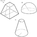
FIG. 4 is a perspective view of patterns applied to simulations according to this exemplary embodiment. -
FIG. 5 is a chart showing results of measuring surface roughness of a phosphor plate according to this exemplary embodiment. - Hereinafter, preferred embodiments of the present invention which can be easily practiced by those of ordinary skill in the art to which the present invention belongs will be described in detail with reference to the accompanying drawings.
-
Phosphor plates more patterns patterns -
FIGS. 1 to 3 are cross-sectional views oflight diffusion units phosphor plates light diffusion units other parts - Referring to
FIGS. 1 to 3 , thephosphor plates phosphor plates - A mixture including two or more phosphors selected from the group consisting of yttrium-aluminum-garnet (YAG)-based, lutetium-aluminum-garnet (LuAG)-based, nitride-based, sulfide-based, and silicate-based phosphors may be used as the phosphor. A phosphor having a wavelength range of 530 nm to 600 nm (green to yellow) may be selected as the phosphor.
- A phosphor in the form of particles or powder may be used as the phosphor. In this case, a phosphor having a particle diameter of 10 µm to 20 µm may be used. In the phosphors, a phosphor having a refractive index of 1.5 to 2.5 is preferably used. The phosphor is mixed at a content of 10% by weight to 20% by weight with respect to the glass frit. In this case, an amount of the mixed phosphor may vary depending on the transmissivity and color difference after sintering. Also, the content of the phosphor may vary depending on a change in thickness. In this case, a smaller amount of the phosphor may be added when the thickness is increased.
- The
phosphor plates - In this case, the compression is performed at a load of 5 tons to 8 tons for 5 to 10 minutes. The compressed phosphor/glass frit mixture is put into a sintering furnace to perform a sintering process. In this case, a temperature and time required to perform a sintering process may be adjusted depending on the glass transition temperatures (Tg) of the phosphor and the glass frit.
- The thickness of the completely sintered
phosphor plates - The
phosphor plates patterns patterns - A photoresist (PR) is applied onto surfaces of the
phosphor plates phosphor plates phosphor plates patterns phosphor plates FIGS. 1 to 3 , but the present invention is not limited thereto. For example, thepatterns patterns FIG. 1 shows a convex pattern,FIG. 2 shows a mixed concave/convex pattern, andFIG. 3 shows a concave pattern. The mixed concave/convex pattern has a structure in which aconcave pattern 214 is further formed within theconvex pattern 212. - The size A of the
patterns patterns patterns - The height C or depth C' of the
patterns convex patterns 212 and 214 (seeFIG. 2 ), the sum of the height C and the depth C' should not be greater than 2 µm. In this exemplary embodiment, a reason for forming thepatterns phosphor plate light source elements patterns - The lighting device according to another aspect of this exemplary embodiment includes
light diffusion units phosphor plates light source elements FIGS. 1 to 3 , the patternedphosphor plates light source elements adhesive layers - The
light source elements light source elements - The
light source elements adhesive layers phosphor plates adhesive layers adhesive layers light source elements light source elements light diffusion units light source elements - Also, although not shown in
FIGS. 1 to 3 , the peripheries of thelight source elements light source elements - Hereinafter, the present invention will be described in further detail with reference to exemplary embodiments thereof. However, it should be understood that the following exemplary embodiments are provided merely to aid in understanding the present invention, and not intended to limit the scope of the present invention.
- The patterns were simulated for pattern shape, position, convex/concave shape, arrangement, and the like under the conditions listed in the following Table 1 to determine light efficiency characteristics.
- The shapes of the patterns are shown in
FIG. 4 .[Table 1] Items Pattern Convex/conc ave Top/bottom Efficiency Efficiency ratio Comparative Example - - - 65.32 1 Pattern 1 Pyramid (4x4x2) Convex Top 72.56 1.1108 Pattern 2 Bottom 64.42 0.9862 Pattern 3 Concave Top 73.11 1.1193 Pattern 4 Bottom 65.8 1.0073 Pattern 5 Hemisphere (Φ4×2) Convex Top 74.77 1.1447 Pattern 6 Bottom 61.64 0.9437 Pattern 7 Concave Top 71.9 1.1007 Pattern 8 Bottom 66.15 1.0127 Pattern 9 Cone 1 (Φ4×2) Convex Top 73.01 1.1177 Pattern 10 Bottom 65.44 1.0018 Pattern 11 Concave Top 72.18 1.1050 Pattern 12 Bottom 64.57 0.9885 Pattern 13 Cone 2 (Φ4×4) Convex Top 73.94 1.1320 Pattern 14 Concave Top 73.57 1.1263 Pattern 15 Sphere_Hexa (Φ4×2) Convex Top 75.58 1.1571 Pattern 16 Concave Top 72.39 1.1082 Pattern 17 Cone_Hexa (Φ4×2) Convex Top 73.16 1.1200 Pattern 18 Concave Top 72.16 1.1047 - (In Table 1, "Hexa" represents a structure in which one unit of the pattern is adjacent to six other units of the pattern, that is, a honeycomb structure)
- From the simulation results, it was revealed that the efficiency was improved by approximately 110% or more when pyramid-shaped, spherical and conical convex/concave patterns were applied to the top surface of the phosphor plate, compared to when there were no patterns. However, it was revealed that the efficiency was slightly improved or degraded when the patterns were applied to the bottom surface of the phosphor plate.
- In the case of the certain shapes, that is, conical and pyramid shapes of the patterns in which the light efficiency is maximized, it is possible to optimize an angle of an incline plane, etc. From the simulation results, it was also revealed that the denser the distance between the patterns was, the more advantageous it was to improving the light efficiency.
- Glass and a phosphor having the following characteristics were mixed to prepare a phosphor plate having a thickness of 160 µm.
-
- Transmittance: 75% (transmittance of glass only based on thickness of 190 µm)
- Refractive index: 1.613
-
- LuAG phosphor having a wavelength of 550 nm, a particle diameter of 15 µm, a content of 15% by weight, and a refractive index of 1.8
- Nitride phosphor having a wavelength of 595 nm, a particle diameter of 15 µm, a content of 2% by weight, and a refractive index of 2.0
- One surface of the phosphor plate thus prepared was subjected to surface polishing to make the surface flat. Thereafter, the surface of the phosphor plate was coated with a photoresist according to a patterned sapphire substrate (PSS) process, exposed to light according to a pattern, and then etched to form patterns on the surface of the phosphor plate (Table 2).
[Table 2] Items Patterning conditions Pattern Pattern height Example 1 PSS pattern 0.4 µm Example 2 PSS pattern 1.0 µm - The phosphor plate thus prepared was subjected to surface polishing without performing a patterning process.
- Each of the light source elements satisfying the requirements listed in the following Table 3 was coated with a silicon adhesive resin (Dow KER-2300 having a refractive index of 1.42) to a thickness of 3 µm. Thereafter, each of the patterned phosphor plates of Examples 1 and 2 and the non-patterned phosphor plate of Comparative Example was attached to the light source element, and optical characteristics were measured. The results are listed in the following Table 4.
[Table 3] p-GaN GaN [Mg] 5.0E18, 2000A MQW In0.14Ga.0xN 4 pairs 25A (InGaN)/80A (GaN) n-GaN GaN (4.5 µm) [Si] 1.0E19 Size 0.98×0.98, 2 Wires White molding material WR-3001 Reflectance: 99.8% Peak at 442 nm, FWHM 21 nm [Table 4] Items Cx Cy Im Relative comparison Example 1 0.3247 0.3273 1905.0 94% Example 2 0.3299 0.3434 2092.4 103% Comparative Example 0.325 0.3358 2027.0 100% - Each of the light source elements satisfying the requirements listed in Table 1 was mounted on an integrating sphere to determine optical characteristics. Thereafter, each of the patterned phosphor plate of Example 1 and the non-patterned phosphor plate of Comparative Example was mounted on an integrating sphere to measure color coordinates (CIE), light flux, light efficiency, and surface roughness. The results are listed in the following Table 5 and shown in
FIG. 5 .[Table 5] Light flux (Lumen) CIE Light efficiency (Lm/Wrad) Note Cx Cy Example 1 (top view) 638.9 0.4425 0.5042 251.2 101.5% Example 1 (bottom view) 638.2 0.4426 0.5039 251.0 101.4% Comparative Example 641.4 0.4412 0.5040 247.5 100% - Referring to Table 5, it can be seen that there was a change between the light flux before patterning and the light flux after patterning. Also, it was revealed that there was no difference in light flux either when a portion of the light source element in contact with the light source element was patterned or vice versa.
- (In
FIG. 5 , Ra represents an average value for the whole section, Rq represents an RMS value of Ra (average value), Rt represents a value obtained by adding the upper and lower maximum values, based on a central line of the whole measurement section, Rz (DIN) represents a value obtained by dividing the whole measurement section into five subsections, determining the maximum values for the respective subsections, and dividing the sum of the maximum values by 5, and a color bar on the right of the drawing represents a depth of a pattern) - The description set forth herein has been merely exemplary and illustrative of exemplary embodiments for the purpose of describing the scope of the present invention, and it will be apparent to those skilled in the art to which the present invention belongs that various modifications and changes can be made without departing from the scope of the present invention. Thus, it should be understood that the exemplary embodiments set forth herein are merely exemplary embodiments for the purpose of illustration only, and not intended to limit the scope of the invention. Accordingly, it should be understood that the scope of the present invention is defined by the appended claims, and that the scope of the present invention defined by the appended claims and their equivalents is intended to cover the scope of the present invention.
Claims (19)
- A phosphor plate comprising:a matrix having one surface and the other surface opposite the one surface;a phosphor dispersed inside the matrix; andan uneven surface disposed on at least one of the one surface and the other surface and having one or more patterns,wherein the patterns occupy 70% to 95% of the whole surface area of either the one surface or the other surface.
- The phosphor plate of claim 1, wherein the uneven surface comprises the pattern having a size (A) of 5.0 µm to 8.0 µm.
- The phosphor plate of claim 2, wherein the patterns have a distance (B) of 7.0 µm to 10 µm, based on a central point of one unit pattern.
- The phosphor plate of claim 1, wherein the uneven surface has a single layout structure including a concave pattern or a convex pattern formed on a surface of the matrix, or a mixed pattern structure in which the concave pattern and the convex pattern are mixed.
- The phosphor plate of claim 4, wherein the pattern has a height (C) or a depth (C') of 0.3 µm to 1.5 µm.
- The phosphor plate of claim 5, wherein the sum of the height (C) and the depth (C') of the pattern is less than or equal to 2 µm when the pattern formed on the uneven surface is a mixed concave/convex pattern.
- The phosphor plate of claim 3, wherein the matrix has a plate-shaped structure comprising a glass material.
- The phosphor plate of claim 3, wherein the phosphor has a refractive index of 1.5 to 2.5.
- The phosphor plate of claim 3, wherein the phosphor comprises two or more phosphors selected from the group consisting of yttrium-aluminum-garnet (YAG)-based, lutetium-aluminum-garnet (LuAG)-based, nitride-based, sulfide-based, and silicate-based phosphors.
- The phosphor plate of claim 9, wherein the phosphor has a wavelength range of 530 nm to 600 nm.
- A lighting device comprising:a light source element; anda phosphor plate disposed below the light source element,wherein the phosphor plate comprises a matrix having one surface and another surface opposite the one surface, a phosphor dispersed inside the matrix, and an uneven surface disposed on either the one surface or the other surface and having one or more patterns, andthe patterns occupy 70% to 95% of the whole surface area of the one surface or the other surface.
- The lighting device of claim 11, wherein a light exit surface of the light source element and the surface opposite the surface on which the uneven surface is formed are disposed in the phosphor plate to be adjacent to each other.
- The lighting device of claim 12, wherein the patterns have a height (C) or a depth (C') of 0.3 µm to 1.5 µm.
- The lighting device of claim 11, wherein the lighting device further comprises an adhesive layer disposed between the light source element and the phosphor plate.
- The lighting device of claim 14, wherein the adhesive layer has a thickness of 2 µm to 5 µm.
- The lighting device of claim 11, wherein the light source element is at least one element selected from the group consisting of a light emitting diode (LED), an organic light emitting diode (OLED), a laser diode (LD), a laser, and a vertical-cavity surface-emitting laser (VCSEL).
- The lighting device of claim 16, wherein the light source element is a blue light source element.
- The lighting device of claim 11, wherein at least one surface of the light source element is coated with a molding material.
- The lighting device of claim 18, wherein the molding material has a reflectance of 99.8% or more.
Applications Claiming Priority (2)
| Application Number | Priority Date | Filing Date | Title |
|---|---|---|---|
| KR1020140101674A KR102310805B1 (en) | 2014-08-07 | 2014-08-07 | Phosphor plate and lighting device including the same |
| PCT/KR2015/008266 WO2016021971A1 (en) | 2014-08-07 | 2015-08-06 | Phosphor plate, and illumination device containing same |
Publications (3)
| Publication Number | Publication Date |
|---|---|
| EP3179160A1 true EP3179160A1 (en) | 2017-06-14 |
| EP3179160A4 EP3179160A4 (en) | 2018-03-14 |
| EP3179160B1 EP3179160B1 (en) | 2021-09-29 |
Family
ID=55264163
Family Applications (1)
| Application Number | Title | Priority Date | Filing Date |
|---|---|---|---|
| EP15829459.5A Active EP3179160B1 (en) | 2014-08-07 | 2015-08-06 | Lighting device including a phosphor plate |
Country Status (5)
| Country | Link |
|---|---|
| US (1) | US10451245B2 (en) |
| EP (1) | EP3179160B1 (en) |
| KR (1) | KR102310805B1 (en) |
| CN (1) | CN106574764B (en) |
| WO (1) | WO2016021971A1 (en) |
Families Citing this family (8)
| Publication number | Priority date | Publication date | Assignee | Title |
|---|---|---|---|---|
| DE102016105988A1 (en) * | 2016-04-01 | 2017-10-05 | Osram Opto Semiconductors Gmbh | Converter for partial conversion of a primary radiation and light-emitting component |
| KR101949893B1 (en) | 2016-11-25 | 2019-02-19 | 광주과학기술원 | Sapphire phosphor plate and white light apparatus based on laser using thereof |
| US11199764B2 (en) | 2018-07-02 | 2021-12-14 | Coretronic Corporation | Light wavelength conversion element and projection apparatus |
| CN110673427B (en) * | 2018-07-02 | 2021-08-24 | 中强光电股份有限公司 | Optical wavelength conversion element and projection device |
| KR102675945B1 (en) * | 2018-09-18 | 2024-06-17 | 삼성전자주식회사 | A light-generating device |
| CN109761501A (en) * | 2019-03-08 | 2019-05-17 | 福建师范大学 | A glass ceramic that can be used for up-conversion laser solid-state lighting and its preparation method and solid-state lighting device |
| US12327978B2 (en) * | 2021-09-23 | 2025-06-10 | Osram Opto Semiconductors Gmbh | Semiconductor light source with a mirror coating and method |
| CN117432973B (en) * | 2023-10-31 | 2024-09-03 | 四川公路工程咨询监理有限公司 | Light source reflecting system special for tunnel energy conservation |
Family Cites Families (22)
| Publication number | Priority date | Publication date | Assignee | Title |
|---|---|---|---|---|
| JP4415572B2 (en) | 2003-06-05 | 2010-02-17 | 日亜化学工業株式会社 | Semiconductor light emitting device and manufacturing method thereof |
| CN1853068A (en) * | 2003-09-19 | 2006-10-25 | 索尼株式会社 | Backlight device and liquid crystal display |
| JP4020092B2 (en) | 2004-03-16 | 2007-12-12 | 住友電気工業株式会社 | Semiconductor light emitting device |
| US7768023B2 (en) * | 2005-10-14 | 2010-08-03 | The Regents Of The University Of California | Photonic structures for efficient light extraction and conversion in multi-color light emitting devices |
| JP4688553B2 (en) * | 2005-04-18 | 2011-05-25 | 京セラ株式会社 | Light emitting device and lighting device |
| JP2007109946A (en) * | 2005-10-14 | 2007-04-26 | Toyoda Gosei Co Ltd | Phosphor plate and light emitting device having the same |
| KR100746749B1 (en) * | 2006-03-15 | 2007-08-09 | (주)케이디티 | Optical excitation sheet |
| KR100723233B1 (en) * | 2006-03-31 | 2007-05-29 | 삼성전기주식회사 | White light emitting device |
| DE102006054330A1 (en) * | 2006-11-17 | 2008-05-21 | Merck Patent Gmbh | Phosphor plates for LEDs made of structured foils |
| CN101459163B (en) * | 2007-12-12 | 2011-07-06 | 富士迈半导体精密工业(上海)有限公司 | Light emitting diode |
| EP2272102B1 (en) * | 2008-03-26 | 2016-06-22 | Panasonic Intellectual Property Management Co., Ltd. | Semiconductor light-emitting apparatus |
| US20140175377A1 (en) * | 2009-04-07 | 2014-06-26 | Soraa, Inc. | Polarized white light devices using non-polar or semipolar gallium containing materials and transparent phosphors |
| KR100969100B1 (en) * | 2010-02-12 | 2010-07-09 | 엘지이노텍 주식회사 | Light emitting device, manufacturing method and light emitting device package |
| EP2602303A4 (en) * | 2010-08-04 | 2014-03-05 | Sekisui Chemical Co Ltd | SURFACE-TREATED FLUORESCENT MATERIAL AND PROCESS FOR PRODUCING SURFACE-TREATED FLUORESCENT MATERIAL |
| KR101805121B1 (en) * | 2010-12-03 | 2017-12-05 | 엘지이노텍 주식회사 | Light emitting device, Light emitting device package and light system |
| US9122000B2 (en) * | 2011-08-24 | 2015-09-01 | Minebea Co., Ltd. | Illuminator using a combination of pseudo-white LED and lens sheet |
| KR101338704B1 (en) * | 2011-12-18 | 2013-12-06 | 엘지이노텍 주식회사 | Light emitting apparatus |
| US9249963B2 (en) * | 2011-11-08 | 2016-02-02 | Lg Innotek Co., Ltd. | Light emitting device |
| US20130258637A1 (en) * | 2012-03-31 | 2013-10-03 | Michael Dongxue Wang | Wavelength-converting structure for a light source |
| KR20130112577A (en) * | 2012-04-04 | 2013-10-14 | 서울반도체 주식회사 | Led lighting apparatus |
| JP2014082401A (en) * | 2012-10-18 | 2014-05-08 | Ushio Inc | Fluorescent light source device |
| US9995458B2 (en) * | 2014-01-13 | 2018-06-12 | Lg Innotek Co., Ltd. | Ceramic phosphor plate and lighting device including the same |
-
2014
- 2014-08-07 KR KR1020140101674A patent/KR102310805B1/en active Active
-
2015
- 2015-08-06 WO PCT/KR2015/008266 patent/WO2016021971A1/en not_active Ceased
- 2015-08-06 CN CN201580042476.4A patent/CN106574764B/en active Active
- 2015-08-06 EP EP15829459.5A patent/EP3179160B1/en active Active
- 2015-08-06 US US15/502,388 patent/US10451245B2/en not_active Expired - Fee Related
Also Published As
| Publication number | Publication date |
|---|---|
| KR20160017948A (en) | 2016-02-17 |
| US20170234506A1 (en) | 2017-08-17 |
| US10451245B2 (en) | 2019-10-22 |
| CN106574764A (en) | 2017-04-19 |
| WO2016021971A1 (en) | 2016-02-11 |
| EP3179160B1 (en) | 2021-09-29 |
| EP3179160A4 (en) | 2018-03-14 |
| CN106574764B (en) | 2019-11-05 |
| KR102310805B1 (en) | 2021-10-08 |
Similar Documents
| Publication | Publication Date | Title |
|---|---|---|
| EP3179160B1 (en) | Lighting device including a phosphor plate | |
| KR101835907B1 (en) | Optoelectronic component | |
| JP5665969B2 (en) | Optoelectronic device and manufacturing method of optoelectronic device | |
| US8222054B2 (en) | LED light source and chromaticity adjustment method for LED light source | |
| TWI725012B (en) | Light source assembly with improved color uniformity | |
| US8803171B2 (en) | Reduced color over angle variation LEDs | |
| CN101449398B (en) | Light emitting element | |
| CN101675536B (en) | Led module with colour conversion layer designed for a homogenous colour distribution | |
| KR20110111390A (en) | Semiconductor lighting system with improved color quality | |
| TW201229434A (en) | Solid-state lamps with light guide and photoluminescence material | |
| TWI566440B (en) | Optoelectronic component and method for manufacturing optoelectronic component | |
| JP2009538532A5 (en) | ||
| TWI497760B (en) | A light-emitting device, an optical characteristic adjusting method, and a light-emitting device manufacturing method | |
| KR20160036489A (en) | Light emitting device | |
| KR20170068518A (en) | Led apparatus employing neodymium-fluorine materials | |
| WO2016056316A1 (en) | Illumination device | |
| KR20160098580A (en) | Optical device and light source module having the same | |
| KR20140141615A (en) | Light source with led chip and luminophore layer | |
| TW201327926A (en) | Light conversion structure and the light emitting device packaging structure using the same | |
| JP2010183035A (en) | Light-emitting device | |
| KR101666844B1 (en) | Optical device and light source module having the same | |
| TW201318216A (en) | Coated diffuser cap for LED illumination device | |
| JP7174290B2 (en) | Light-emitting device and method for manufacturing light-emitting device | |
| JP2023001230A (en) | Light-emitting device and method for manufacturing light-emitting device | |
| JP2006108180A (en) | Reflector, light-emitting diode and package therefor |
Legal Events
| Date | Code | Title | Description |
|---|---|---|---|
| STAA | Information on the status of an ep patent application or granted ep patent |
Free format text: STATUS: THE INTERNATIONAL PUBLICATION HAS BEEN MADE |
|
| PUAI | Public reference made under article 153(3) epc to a published international application that has entered the european phase |
Free format text: ORIGINAL CODE: 0009012 |
|
| STAA | Information on the status of an ep patent application or granted ep patent |
Free format text: STATUS: REQUEST FOR EXAMINATION WAS MADE |
|
| 17P | Request for examination filed |
Effective date: 20170127 |
|
| AK | Designated contracting states |
Kind code of ref document: A1 Designated state(s): AL AT BE BG CH CY CZ DE DK EE ES FI FR GB GR HR HU IE IS IT LI LT LU LV MC MK MT NL NO PL PT RO RS SE SI SK SM TR |
|
| AX | Request for extension of the european patent |
Extension state: BA ME |
|
| DAV | Request for validation of the european patent (deleted) | ||
| DAX | Request for extension of the european patent (deleted) | ||
| A4 | Supplementary search report drawn up and despatched |
Effective date: 20180214 |
|
| RIC1 | Information provided on ipc code assigned before grant |
Ipc: F21K 9/64 20160101ALN20180208BHEP Ipc: H01L 33/32 20100101ALN20180208BHEP Ipc: H01L 33/06 20100101ALN20180208BHEP Ipc: F21K 9/60 20160101AFI20180208BHEP Ipc: H01L 33/60 20100101ALN20180208BHEP Ipc: H01L 33/50 20100101ALI20180208BHEP |
|
| STAA | Information on the status of an ep patent application or granted ep patent |
Free format text: STATUS: EXAMINATION IS IN PROGRESS |
|
| 17Q | First examination report despatched |
Effective date: 20200706 |
|
| REG | Reference to a national code |
Ref country code: DE Ref legal event code: R079 Ref document number: 602015073755 Country of ref document: DE Free format text: PREVIOUS MAIN CLASS: F21V0005000000 Ipc: H01L0033500000 |
|
| RIC1 | Information provided on ipc code assigned before grant |
Ipc: F21K 9/64 20160101ALN20210310BHEP Ipc: H01L 33/50 20100101AFI20210310BHEP |
|
| GRAP | Despatch of communication of intention to grant a patent |
Free format text: ORIGINAL CODE: EPIDOSNIGR1 |
|
| STAA | Information on the status of an ep patent application or granted ep patent |
Free format text: STATUS: GRANT OF PATENT IS INTENDED |
|
| INTG | Intention to grant announced |
Effective date: 20210420 |
|
| GRAS | Grant fee paid |
Free format text: ORIGINAL CODE: EPIDOSNIGR3 |
|
| GRAA | (expected) grant |
Free format text: ORIGINAL CODE: 0009210 |
|
| STAA | Information on the status of an ep patent application or granted ep patent |
Free format text: STATUS: THE PATENT HAS BEEN GRANTED |
|
| AK | Designated contracting states |
Kind code of ref document: B1 Designated state(s): AL AT BE BG CH CY CZ DE DK EE ES FI FR GB GR HR HU IE IS IT LI LT LU LV MC MK MT NL NO PL PT RO RS SE SI SK SM TR |
|
| REG | Reference to a national code |
Ref country code: GB Ref legal event code: FG4D |
|
| REG | Reference to a national code |
Ref country code: CH Ref legal event code: EP Ref country code: AT Ref legal event code: REF Ref document number: 1434981 Country of ref document: AT Kind code of ref document: T Effective date: 20211015 |
|
| REG | Reference to a national code |
Ref country code: DE Ref legal event code: R096 Ref document number: 602015073755 Country of ref document: DE |
|
| REG | Reference to a national code |
Ref country code: IE Ref legal event code: FG4D |
|
| REG | Reference to a national code |
Ref country code: LT Ref legal event code: MG9D |
|
| PG25 | Lapsed in a contracting state [announced via postgrant information from national office to epo] |
Ref country code: NO Free format text: LAPSE BECAUSE OF FAILURE TO SUBMIT A TRANSLATION OF THE DESCRIPTION OR TO PAY THE FEE WITHIN THE PRESCRIBED TIME-LIMIT Effective date: 20211229 Ref country code: FI Free format text: LAPSE BECAUSE OF FAILURE TO SUBMIT A TRANSLATION OF THE DESCRIPTION OR TO PAY THE FEE WITHIN THE PRESCRIBED TIME-LIMIT Effective date: 20210929 Ref country code: LT Free format text: LAPSE BECAUSE OF FAILURE TO SUBMIT A TRANSLATION OF THE DESCRIPTION OR TO PAY THE FEE WITHIN THE PRESCRIBED TIME-LIMIT Effective date: 20210929 Ref country code: BG Free format text: LAPSE BECAUSE OF FAILURE TO SUBMIT A TRANSLATION OF THE DESCRIPTION OR TO PAY THE FEE WITHIN THE PRESCRIBED TIME-LIMIT Effective date: 20211229 Ref country code: HR Free format text: LAPSE BECAUSE OF FAILURE TO SUBMIT A TRANSLATION OF THE DESCRIPTION OR TO PAY THE FEE WITHIN THE PRESCRIBED TIME-LIMIT Effective date: 20210929 Ref country code: SE Free format text: LAPSE BECAUSE OF FAILURE TO SUBMIT A TRANSLATION OF THE DESCRIPTION OR TO PAY THE FEE WITHIN THE PRESCRIBED TIME-LIMIT Effective date: 20210929 Ref country code: RS Free format text: LAPSE BECAUSE OF FAILURE TO SUBMIT A TRANSLATION OF THE DESCRIPTION OR TO PAY THE FEE WITHIN THE PRESCRIBED TIME-LIMIT Effective date: 20210929 |
|
| REG | Reference to a national code |
Ref country code: NL Ref legal event code: MP Effective date: 20210929 |
|
| REG | Reference to a national code |
Ref country code: AT Ref legal event code: MK05 Ref document number: 1434981 Country of ref document: AT Kind code of ref document: T Effective date: 20210929 |
|
| PG25 | Lapsed in a contracting state [announced via postgrant information from national office to epo] |
Ref country code: LV Free format text: LAPSE BECAUSE OF FAILURE TO SUBMIT A TRANSLATION OF THE DESCRIPTION OR TO PAY THE FEE WITHIN THE PRESCRIBED TIME-LIMIT Effective date: 20210929 Ref country code: GR Free format text: LAPSE BECAUSE OF FAILURE TO SUBMIT A TRANSLATION OF THE DESCRIPTION OR TO PAY THE FEE WITHIN THE PRESCRIBED TIME-LIMIT Effective date: 20211230 |
|
| PG25 | Lapsed in a contracting state [announced via postgrant information from national office to epo] |
Ref country code: AT Free format text: LAPSE BECAUSE OF FAILURE TO SUBMIT A TRANSLATION OF THE DESCRIPTION OR TO PAY THE FEE WITHIN THE PRESCRIBED TIME-LIMIT Effective date: 20210929 |
|
| PG25 | Lapsed in a contracting state [announced via postgrant information from national office to epo] |
Ref country code: IS Free format text: LAPSE BECAUSE OF FAILURE TO SUBMIT A TRANSLATION OF THE DESCRIPTION OR TO PAY THE FEE WITHIN THE PRESCRIBED TIME-LIMIT Effective date: 20220129 Ref country code: SK Free format text: LAPSE BECAUSE OF FAILURE TO SUBMIT A TRANSLATION OF THE DESCRIPTION OR TO PAY THE FEE WITHIN THE PRESCRIBED TIME-LIMIT Effective date: 20210929 Ref country code: RO Free format text: LAPSE BECAUSE OF FAILURE TO SUBMIT A TRANSLATION OF THE DESCRIPTION OR TO PAY THE FEE WITHIN THE PRESCRIBED TIME-LIMIT Effective date: 20210929 Ref country code: PT Free format text: LAPSE BECAUSE OF FAILURE TO SUBMIT A TRANSLATION OF THE DESCRIPTION OR TO PAY THE FEE WITHIN THE PRESCRIBED TIME-LIMIT Effective date: 20220131 Ref country code: PL Free format text: LAPSE BECAUSE OF FAILURE TO SUBMIT A TRANSLATION OF THE DESCRIPTION OR TO PAY THE FEE WITHIN THE PRESCRIBED TIME-LIMIT Effective date: 20210929 Ref country code: NL Free format text: LAPSE BECAUSE OF FAILURE TO SUBMIT A TRANSLATION OF THE DESCRIPTION OR TO PAY THE FEE WITHIN THE PRESCRIBED TIME-LIMIT Effective date: 20210929 Ref country code: ES Free format text: LAPSE BECAUSE OF FAILURE TO SUBMIT A TRANSLATION OF THE DESCRIPTION OR TO PAY THE FEE WITHIN THE PRESCRIBED TIME-LIMIT Effective date: 20210929 Ref country code: EE Free format text: LAPSE BECAUSE OF FAILURE TO SUBMIT A TRANSLATION OF THE DESCRIPTION OR TO PAY THE FEE WITHIN THE PRESCRIBED TIME-LIMIT Effective date: 20210929 Ref country code: CZ Free format text: LAPSE BECAUSE OF FAILURE TO SUBMIT A TRANSLATION OF THE DESCRIPTION OR TO PAY THE FEE WITHIN THE PRESCRIBED TIME-LIMIT Effective date: 20210929 Ref country code: AL Free format text: LAPSE BECAUSE OF FAILURE TO SUBMIT A TRANSLATION OF THE DESCRIPTION OR TO PAY THE FEE WITHIN THE PRESCRIBED TIME-LIMIT Effective date: 20210929 |
|
| REG | Reference to a national code |
Ref country code: DE Ref legal event code: R097 Ref document number: 602015073755 Country of ref document: DE |
|
| PG25 | Lapsed in a contracting state [announced via postgrant information from national office to epo] |
Ref country code: DK Free format text: LAPSE BECAUSE OF FAILURE TO SUBMIT A TRANSLATION OF THE DESCRIPTION OR TO PAY THE FEE WITHIN THE PRESCRIBED TIME-LIMIT Effective date: 20210929 |
|
| PLBE | No opposition filed within time limit |
Free format text: ORIGINAL CODE: 0009261 |
|
| STAA | Information on the status of an ep patent application or granted ep patent |
Free format text: STATUS: NO OPPOSITION FILED WITHIN TIME LIMIT |
|
| 26N | No opposition filed |
Effective date: 20220630 |
|
| PG25 | Lapsed in a contracting state [announced via postgrant information from national office to epo] |
Ref country code: SI Free format text: LAPSE BECAUSE OF FAILURE TO SUBMIT A TRANSLATION OF THE DESCRIPTION OR TO PAY THE FEE WITHIN THE PRESCRIBED TIME-LIMIT Effective date: 20210929 |
|
| PG25 | Lapsed in a contracting state [announced via postgrant information from national office to epo] |
Ref country code: IT Free format text: LAPSE BECAUSE OF FAILURE TO SUBMIT A TRANSLATION OF THE DESCRIPTION OR TO PAY THE FEE WITHIN THE PRESCRIBED TIME-LIMIT Effective date: 20210929 |
|
| PG25 | Lapsed in a contracting state [announced via postgrant information from national office to epo] |
Ref country code: MC Free format text: LAPSE BECAUSE OF FAILURE TO SUBMIT A TRANSLATION OF THE DESCRIPTION OR TO PAY THE FEE WITHIN THE PRESCRIBED TIME-LIMIT Effective date: 20210929 |
|
| REG | Reference to a national code |
Ref country code: CH Ref legal event code: PL |
|
| GBPC | Gb: european patent ceased through non-payment of renewal fee |
Effective date: 20220806 |
|
| PG25 | Lapsed in a contracting state [announced via postgrant information from national office to epo] |
Ref country code: LU Free format text: LAPSE BECAUSE OF NON-PAYMENT OF DUE FEES Effective date: 20220806 Ref country code: LI Free format text: LAPSE BECAUSE OF NON-PAYMENT OF DUE FEES Effective date: 20220831 Ref country code: CH Free format text: LAPSE BECAUSE OF NON-PAYMENT OF DUE FEES Effective date: 20220831 |
|
| REG | Reference to a national code |
Ref country code: BE Ref legal event code: MM Effective date: 20220831 |
|
| PG25 | Lapsed in a contracting state [announced via postgrant information from national office to epo] |
Ref country code: IE Free format text: LAPSE BECAUSE OF NON-PAYMENT OF DUE FEES Effective date: 20220806 Ref country code: FR Free format text: LAPSE BECAUSE OF NON-PAYMENT OF DUE FEES Effective date: 20220831 |
|
| PG25 | Lapsed in a contracting state [announced via postgrant information from national office to epo] |
Ref country code: BE Free format text: LAPSE BECAUSE OF NON-PAYMENT OF DUE FEES Effective date: 20220831 |
|
| PG25 | Lapsed in a contracting state [announced via postgrant information from national office to epo] |
Ref country code: GB Free format text: LAPSE BECAUSE OF NON-PAYMENT OF DUE FEES Effective date: 20220806 |
|
| PG25 | Lapsed in a contracting state [announced via postgrant information from national office to epo] |
Ref country code: HU Free format text: LAPSE BECAUSE OF FAILURE TO SUBMIT A TRANSLATION OF THE DESCRIPTION OR TO PAY THE FEE WITHIN THE PRESCRIBED TIME-LIMIT; INVALID AB INITIO Effective date: 20150806 |
|
| PG25 | Lapsed in a contracting state [announced via postgrant information from national office to epo] |
Ref country code: SM Free format text: LAPSE BECAUSE OF FAILURE TO SUBMIT A TRANSLATION OF THE DESCRIPTION OR TO PAY THE FEE WITHIN THE PRESCRIBED TIME-LIMIT Effective date: 20210929 Ref country code: CY Free format text: LAPSE BECAUSE OF FAILURE TO SUBMIT A TRANSLATION OF THE DESCRIPTION OR TO PAY THE FEE WITHIN THE PRESCRIBED TIME-LIMIT Effective date: 20210929 |
|
| PG25 | Lapsed in a contracting state [announced via postgrant information from national office to epo] |
Ref country code: MK Free format text: LAPSE BECAUSE OF FAILURE TO SUBMIT A TRANSLATION OF THE DESCRIPTION OR TO PAY THE FEE WITHIN THE PRESCRIBED TIME-LIMIT Effective date: 20210929 |
|
| PG25 | Lapsed in a contracting state [announced via postgrant information from national office to epo] |
Ref country code: MT Free format text: LAPSE BECAUSE OF FAILURE TO SUBMIT A TRANSLATION OF THE DESCRIPTION OR TO PAY THE FEE WITHIN THE PRESCRIBED TIME-LIMIT Effective date: 20210929 |
|
| REG | Reference to a national code |
Ref country code: DE Ref legal event code: R079 Ref document number: 602015073755 Country of ref document: DE Free format text: PREVIOUS MAIN CLASS: H01L0033500000 Ipc: H10H0020851000 |
|
| PGFP | Annual fee paid to national office [announced via postgrant information from national office to epo] |
Ref country code: DE Payment date: 20250721 Year of fee payment: 11 |
|
| PG25 | Lapsed in a contracting state [announced via postgrant information from national office to epo] |
Ref country code: TR Free format text: LAPSE BECAUSE OF FAILURE TO SUBMIT A TRANSLATION OF THE DESCRIPTION OR TO PAY THE FEE WITHIN THE PRESCRIBED TIME-LIMIT Effective date: 20210929 |