EP3176934A1 - Power conversion device - Google Patents
Power conversion device Download PDFInfo
- Publication number
- EP3176934A1 EP3176934A1 EP15827427.4A EP15827427A EP3176934A1 EP 3176934 A1 EP3176934 A1 EP 3176934A1 EP 15827427 A EP15827427 A EP 15827427A EP 3176934 A1 EP3176934 A1 EP 3176934A1
- Authority
- EP
- European Patent Office
- Prior art keywords
- command
- arm
- voltage
- phase
- control
- Prior art date
- Legal status (The legal status is an assumption and is not a legal conclusion. Google has not performed a legal analysis and makes no representation as to the accuracy of the status listed.)
- Granted
Links
Images




Classifications
-
- H—ELECTRICITY
- H02—GENERATION; CONVERSION OR DISTRIBUTION OF ELECTRIC POWER
- H02M—APPARATUS FOR CONVERSION BETWEEN AC AND AC, BETWEEN AC AND DC, OR BETWEEN DC AND DC, AND FOR USE WITH MAINS OR SIMILAR POWER SUPPLY SYSTEMS; CONVERSION OF DC OR AC INPUT POWER INTO SURGE OUTPUT POWER; CONTROL OR REGULATION THEREOF
- H02M7/00—Conversion of AC power input into DC power output; Conversion of DC power input into AC power output
- H02M7/42—Conversion of DC power input into AC power output without possibility of reversal
- H02M7/44—Conversion of DC power input into AC power output without possibility of reversal by static converters
- H02M7/48—Conversion of DC power input into AC power output without possibility of reversal by static converters using discharge tubes with control electrode or semiconductor devices with control electrode
- H02M7/483—Converters with outputs that each can have more than two voltages levels
-
- H—ELECTRICITY
- H02—GENERATION; CONVERSION OR DISTRIBUTION OF ELECTRIC POWER
- H02M—APPARATUS FOR CONVERSION BETWEEN AC AND AC, BETWEEN AC AND DC, OR BETWEEN DC AND DC, AND FOR USE WITH MAINS OR SIMILAR POWER SUPPLY SYSTEMS; CONVERSION OF DC OR AC INPUT POWER INTO SURGE OUTPUT POWER; CONTROL OR REGULATION THEREOF
- H02M1/00—Details of apparatus for conversion
- H02M1/12—Arrangements for reducing harmonics from AC input or output
-
- H—ELECTRICITY
- H02—GENERATION; CONVERSION OR DISTRIBUTION OF ELECTRIC POWER
- H02M—APPARATUS FOR CONVERSION BETWEEN AC AND AC, BETWEEN AC AND DC, OR BETWEEN DC AND DC, AND FOR USE WITH MAINS OR SIMILAR POWER SUPPLY SYSTEMS; CONVERSION OF DC OR AC INPUT POWER INTO SURGE OUTPUT POWER; CONTROL OR REGULATION THEREOF
- H02M7/00—Conversion of AC power input into DC power output; Conversion of DC power input into AC power output
- H02M7/02—Conversion of AC power input into DC power output without possibility of reversal
- H02M7/04—Conversion of AC power input into DC power output without possibility of reversal by static converters
- H02M7/12—Conversion of AC power input into DC power output without possibility of reversal by static converters using discharge tubes with control electrode or semiconductor devices with control electrode
- H02M7/21—Conversion of AC power input into DC power output without possibility of reversal by static converters using discharge tubes with control electrode or semiconductor devices with control electrode using devices of a triode or transistor type requiring continuous application of a control signal
- H02M7/217—Conversion of AC power input into DC power output without possibility of reversal by static converters using discharge tubes with control electrode or semiconductor devices with control electrode using devices of a triode or transistor type requiring continuous application of a control signal using semiconductor devices only
-
- H—ELECTRICITY
- H02—GENERATION; CONVERSION OR DISTRIBUTION OF ELECTRIC POWER
- H02M—APPARATUS FOR CONVERSION BETWEEN AC AND AC, BETWEEN AC AND DC, OR BETWEEN DC AND DC, AND FOR USE WITH MAINS OR SIMILAR POWER SUPPLY SYSTEMS; CONVERSION OF DC OR AC INPUT POWER INTO SURGE OUTPUT POWER; CONTROL OR REGULATION THEREOF
- H02M7/00—Conversion of AC power input into DC power output; Conversion of DC power input into AC power output
- H02M7/42—Conversion of DC power input into AC power output without possibility of reversal
- H02M7/44—Conversion of DC power input into AC power output without possibility of reversal by static converters
- H02M7/48—Conversion of DC power input into AC power output without possibility of reversal by static converters using discharge tubes with control electrode or semiconductor devices with control electrode
- H02M7/483—Converters with outputs that each can have more than two voltages levels
- H02M7/4835—Converters with outputs that each can have more than two voltages levels comprising two or more cells, each including a switchable capacitor, the capacitors having a nominal charge voltage which corresponds to a given fraction of the input voltage, and the capacitors being selectively connected in series to determine the instantaneous output voltage
Definitions
- the present invention relates to a power conversion device for performing power conversion between three-phase AC, and DC, and in particular, to a large-capacity power conversion device with multi-connected converters.
- the converter output is high voltage or large current, and therefore, many large-capacity power conversion devices are configured with a plurality of converters multi-connected in series or parallel.
- Multi-connecting converters can not only increase the converter capacity, but also reduce harmonics contained in an output voltage waveform by synthesizing outputs, and as a result, can reduce harmonic current flowing to a grid.
- multilevel converter in which outputs of a plurality of converters are connected in cascade, and one of such multilevel converters is a modular multilevel converter.
- Each arm of the modular multilevel converter is composed of a plurality of converter cells connected in cascade.
- Each of a first arm and a second arm for each phase of the conventional modular multilevel converter has a chopper cell (converter cell) and a reactor.
- the chopper cell has two semiconductor switches connected in series to each other, and a DC capacitor connected in parallel thereto.
- the same number of chopper cells are connected in cascade via their respective output terminals.
- Control for each phase of the conventional modular multilevel converter comprises: average value control for causing the average value of voltage values of all DC capacitors to follow a capacitor voltage command value; individual balance control for causing the voltage value of each DC capacitor to follow the capacitor voltage command value; and arm balance control for causing the average value of voltage values of all the DC capacitors in the first arm and the average value of voltage values of all the DC capacitors in the second arm to coincide with each other.
- a voltage command value is calculated so as to control circulating current which circulates in the modular multilevel converter without flowing to the outside of the modular multilevel converter, and to control AC current for each phase (for example, see Patent Document 1 and Non-Patent Document 1).
- a control device in a power conversion device used for DC power transmission, a control device is often designed with respect to a specific operation point, and if an AC grid varies, the system might become unstable.
- a DC current path of a DC power transmission system is a long-distance cable
- the inductance and the electrostatic capacitance of the cable increase and the resonance frequency of the DC current path decreases, and it is necessary to perform control that is stable against resonance of the DC circuit and ensures response performance.
- Non-Patent Document 1 IEEJ transactions D (on industry applications) Vol. 131, No. 1, 2011 (pages 84 to 92 )
- the conventional power conversion device using a modular multilevel converter performs control under the assumption that the inductance components of the positive arm and the negative arm are equal to each other. If the inductance components of the positive arm and the negative arm are different from each other, a fluctuation component contained in output voltages of the positive arm and the negative arm flows out to the DC circuit. In particular, in the case where the inductance and the electrostatic capacitance of the DC current path are great and the resonance frequency of the DC current path is low, there is a problem that the fluctuation component having flowed out to the DC circuit excites the DC circuit and current of the DC circuit oscillates.
- the disturbance generation source of DC circuit resonance is the power conversion device (modular multilevel converter), and therefore current oscillation of the DC circuit cannot be suppressed by the control shown in the above Patent Document 2, i.e., the method of controlling the DC voltage.
- the present invention has been made to solve the above problems, and an object of the present invention is to obtain a power conversion device capable of, even if the positive arm and the negative arm have different inductance components, suppressing a voltage fluctuation component flowing out to the DC side and suppressing current oscillation of the connected DC circuit.
- a power conversion device comprises: a power converter for performing power conversion between three-phase AC, and DC, the power converter including a plurality of leg circuits each having a positive arm and a negative arm connected in series, outputs of the positive arm and the negative arm being connected to each phase AC line, the plurality of leg circuits being connected in parallel between positive and negative DC buses; and a control device for controlling the power converter.
- Each of the positive arm and the negative arm of each leg circuit is composed of one or a plurality of converter cells connected in series and including: a series unit of a plurality of semiconductor switching elements connected in series to each other; and a DC capacitor connected in parallel to the series unit.
- the control device comprises a voltage command generating unit for generating a first voltage command for the positive arm and a second voltage command for the negative arm, to perform output control for each converter cell in the positive arm and the negative arm by PWM control.
- the voltage command generating unit comprises: an AC current control unit for generating an AC control command for controlling an AC current component flowing through each phase AC line; a circulating current control unit for calculating a circulation control command for controlling a circulating current component for each phase which circulates between the leg circuits; and a command distributing unit for determining the first voltage command and the second voltage command on the basis of the AC control command, the circulation control command, and a voltage command value for voltage between the DC buses.
- the circulating current control unit comprises: a compensator for calculating a first control command so that circulating current for each phase which circulates between the leg circuits approaches a circulating current command value; and a suppression unit for generating a second control command for suppressing at least one of a double-frequency component and a quadruple-frequency component of an AC fundamental wave, which are contained in the calculated first control command.
- the circulating current control unit calculates the circulation control command by combining the first control command and the second control command.
- the power conversion device of the present invention is capable of, even if the positive arm and the negative arm have different inductance components, suppressing a fluctuation component flowing out to the DC side and suppressing current oscillation of the connected DC circuit.
- the power conversion device of the present invention is capable of suppressing flowing out of a current oscillation component including at least one of a double-frequency component and a quadruple-frequency component of the AC fundamental wave, to the three-phase AC side, and thereby enabling reliable control of the power conversion device.
- FIG. 1 is a schematic configuration diagram of the power conversion device according to Embodiment 1 of the present invention.
- the power conversion device comprises a power converter 1 as a main circuit, and a control device 20 for controlling the power converter 1.
- the power converter 1 performs power conversion between three-phase AC, and DC.
- the AC side of the power converter 1 is connected via an interconnection transformer 13 to a three-phase AC power supply 14 which is a grid as a three-phase AC circuit, and the DC side is connected via an impedance 15 to a DC power supply 16 which is a DC grid.
- connection to the AC power supply 14 may be made via an interconnection reactor instead of the interconnection transformer 13.
- the DC side of the power converter 1 may be connected to a DC load or may be connected to another power conversion device that performs DC output.
- Each phase of the power converter 1 is composed of a leg circuit 4 in which a positive arm 5 and a negative arm 6 are connected in series and an AC terminal 7 which is the connection point therebetween is connected to each phase AC line.
- the three leg circuits 4 are connected in parallel between positive and negative DC buses 2 and 3.
- the positive arm 5 and the negative arm 6 of each leg circuit 4 are respectively composed of cell groups 5a and 6a each including one or more converter cells 10 connected in series, and a positive reactor 9p and a negative reactor 9n are provided in series in the respective arms.
- the positive reactor 9p and the negative reactor 9n have different reactances, and are connected on the AC terminal 7 side, to form a reactor 8 having three terminals.
- the locations where the positive reactor 9p and the negative reactor 9n are provided may be any locations in the arms 5 and 6, and a plurality of reactors may be provided in each arm.
- the control device 20 comprises: a voltage command generating unit 21 for generating a positive arm voltage command Vp + which is a first voltage command, and a negative arm voltage command Vp- which is a second voltage command; and a PWM circuit 22, to generate a gate signal 22a, thereby controlling each converter cell 10 in the positive arm 5 and the negative arm 6 for each phase.
- Positive arm current ip + and negative arm current ip- respectively flowing through the positive arm 5 and the negative arm 6 for each phase, and AC current ip flowing through each phase AC line are detected by a current detector (not shown) and input to the control device 20. Further, each phase voltage (hereinafter, referred to as AC voltage Vsp) of the AC power supply 14 detected by a voltage detector (not shown), neutral point voltage Vsn of the power converter 1, and a command value (hereinafter, a DC voltage command value Vdc) for voltage of the DC power supply 16 which is voltage between the DC buses, are input to the control device 20.
- AC current ip for each phase the one calculated from the positive arm current ip + and the negative arm current ip-respectively flowing through the positive arm 5 and the negative arm 6 for each phase, may be used.
- the voltage command generating unit 21 generates the positive arm voltage command Vp + for the positive arm 5 for each phase, and the negative arm voltage command Vp- for the negative arm 6 for each phase, on the basis of the input information about voltage and current. Then, the PWM circuit 22 generates the gate signal 22a through pulse width modulation control (PWM control) on the basis of each voltage command Vp + , Vp - .
- PWM control pulse width modulation control
- control device 20 The details of the configuration and operation of the control device 20 will be described later.
- FIG. 2 shows a configuration example of each converter cell 10.
- FIG. 2 shows the converter cell 10 in which a half-bridge configuration is employed.
- the converter cell 10 in FIG. 2 is composed of: a series unit 32 of a plurality of (in this case, two) semiconductor switching elements 30 (hereinafter, simply referred to as switching elements) to which diodes 31 are respectively connected in antiparallel; and a DC capacitor 34 connected in parallel to the series unit 32 and for smoothing DC voltage.
- Each switching element 30 is formed of a self-turn-off switching element such as an IGBT (Insulated Gate Bipolar Transistor) or a GCT (Gate Commutated Turn-off thyristor), and the diodes 31 are respectively connected in antiparallel thereto, to form switches 33P and 33N.
- both terminals of the switching element 30 of the switch 33N are used as output terminals, and through ON/OFF control of the switching element 30, voltage of the DC capacitor 34 and zero voltage are output from the output terminals.
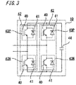
- FIG. 3 shows another configuration example of each converter cell 10.
- FIG. 3 shows the converter cell 10 in which a full-bridge configuration is employed.
- the converter cell 10 in FIG. 3 is composed of: two series units 42 connected in parallel; and a DC capacitor 44 connected in parallel to the series units 42 and for smoothing DC voltage.
- Each series unit 42 is composed of a plurality of (in this case, two) switching elements 40 connected in series, to which diodes 41 are respectively connected in antiparallel.
- Each switching element 40 is formed of a self-turn-off switching element such as an IGBT or a GCT, and the diodes 41 are respectively connected in antiparallel thereto, to form switches 43P and 43N.
- terminals of the switching elements 40 corresponding to the intermediate connection points of the respective series units 42 are used as output terminals, and through ON/OFF control of the switching elements 40, positive voltage and negative voltage at both terminals of the DC capacitor 44 and zero voltage are output from the output terminals.
- the converter cell 10 is not limited to the configurations shown in FIG. 2 and FIG. 3 as long as the converter cell 10 is composed of a series unit of a plurality of switching elements and a DC capacitor connected in parallel to the series unit, and selectively outputs voltage of the DC capacitor through switching operation.
- control device 20 Next, the details of the control device 20 will be described.
- the power converter 1 Since the power converter 1 outputs DC and AC, the power converter 1 needs to be controlled both on the DC side and the AC side. Further, since circulating current izp which circulates between the positive and negative arms without contributing to the AC-side output or the DC-side output flows in the power converter 1, it is necessary to control the circulating current izp in addition to the DC-side control and the AC-side control. In this case, since the AC terminals 7 are interconnected with the AC power supply 14 of the grid, it is necessary to output AC voltage needed for the AC-side control from the power converter 1, and control of performing compensation by feeding forward the AC voltage Vsp for each phase at the AC interconnection point is performed.
- FIG. 4 is a block diagram showing a configuration example of the control device 20.
- FIG. 5 shows the details of a circulating current control unit 24 in the control device 20.
- the control device 20 comprises the voltage command generating unit 21 and the PWM circuit 22.
- the voltage command generating unit 21 comprises: an AC current control unit 23 for controlling the AC current ip; and the circulating current control unit 24 for controlling the circulating current izp for each phase which circulates in the power converter 1, and further comprises a command distributing unit 25 for determining the positive arm voltage command Vp + and the negative arm voltage command Vp- for each phase.
- the AC current control unit 23 calculates an AC control command Vcp which is a voltage command so that the deviation between the detected AC current ip and a set AC current command becomes zero. That is, the AC current control unit 23 calculates the AC control command Vcp for controlling the AC current ip flowing through each phase AC line to follow the AC current command.
- the circulating current control unit 24 calculates a circulation control command Vzp for controlling the circulating current izp for each phase to follow a set circulating current command value, e.g., zero.
- the circulating current control unit 24 comprises: a compensator 27 for calculating a first control command ⁇ Vzp so that the circulating current izp for each phase approaches the circulating current command value; a suppression unit 28 for suppressing a double-frequency component and a quadruple-frequency component of an AC fundamental wave, which are contained in the calculated first control command ⁇ Vzp; and a subtractor 26 and an adder 29.
- the circulating current izp for each phase can be calculated from the positive arm current ip + and the negative arm current ip- respectively flowing through the positive arm 5 and the negative arm 6 for each phase.
- nf an n-th order frequency of the AC fundamental wave
- nf component an n-th order frequency component of the AC fundamental wave
- the subtractor 26 calculates a deviation ⁇ izp between the set circulating current command value and the circulating current izp for each phase, and the compensator 27 calculates a first control command ⁇ Vzp which is a voltage command value so that low-frequency components of the deviation ⁇ izp, e.g., a DC component and a 1f component become zero.
- the suppression unit 28 calculates a second control command ⁇ Vfzp which is a voltage command value for extracting and suppressing a 2f component and a 4f component of the first control command ⁇ Vzp from the compensator 27.
- the adder 29 adds the second control command ⁇ Vfzp to the first control command ⁇ Vzp which is output of the compensator 27, whereby the circulation control command Vzp is calculated.
- the command distributing unit 25 receives the calculated AC control command Vcp and circulation control command Vzp, the DC voltage command value Vdc, and the neutral point voltage Vsn, and further receives the AC voltage Vsp for each phase as a feedforward term.
- the neutral point voltage Vsn is calculated from voltage of the DC power supply 16.
- the DC voltage command value VDC may be given by DC output control, or may be a constant value.
- the neutral point voltage Vsn is calculated from the AC voltage Vsp and voltage of the DC power supply 16.
- the command distributing unit 25 subtracts voltage drop portions due to inductance components in the arms 5 and 6 from respective voltages assigned as outputs of the positive arm 5 and the negative arm 6, to distribute voltage components, thereby determining the positive arm voltage command Vp + for the positive arm 5 for each phase and the negative arm voltage command Vp- for the negative arm 6 for each phase.
- the positive arm voltage command Vp + and the negative arm voltage command Vp- for each phase thus generated by the voltage command generating unit 21 become output voltage commands for controlling the AC current ip and the circulating current izp to respectively follow the AC current command and the circulating current command value, controlling voltage of the DC power supply 16 to be the DC voltage command value Vdc, and performing feedforward control of the AC voltage Vsp.
- the PWM circuit 22 generates the gate signal 22a to perform PWM control for each converter cell 10 in the positive arm 5 and the negative arm 6 for each phase, on the basis of the positive arm voltage command Vp + and the negative arm voltage command Vp - .
- the switching element 30 (40) in each converter cell 10 is drive-controlled, so that output voltage of the power converter 1 is controlled to be a desired value.
- FIG. 6 is a diagram showing voltages and currents at various sections on a circuit, for one phase of the power converter 1.
- LAC denotes an inductance of the interconnection transformer 13
- Lc + denotes an inductance of the positive reactor 9p
- Lc - denotes an inductance of the negative reactor 9n.
- the positive arm voltage command Vp + is a command value for voltage to be output from the cell group 5a including the converter cells 10 connected in series in the positive arm 5
- the negative arm voltage command Vp- is a command value for voltage to be output from the cell group 6a including the converter cells 10 connected in series in the negative arm 6.
- the output voltages of the cell groups 5a and 6a are controlled to be Vp + and Vp - .
- voltage of the DC power supply 16 is controlled to be the DC voltage command value Vdc.
- the positive arm current ip + and the negative arm current ip - are represented by the following Expression (1) and Expression (2).
- Mathematical 1 Mathematical 1 ip + ip 2 + izp
- Mathematical 2 Mathematical 2 ip ⁇ ⁇ ip 2 + izp
- Vp + (v) and Vp - (v) for controlling voltage are represented as follows.
- Vp + (i) and Vp - (i) for controlling current are represented as follows.
- the AC control command Vcp and the circulation control command Vzp only need to be represented by the following Expression (9).
- Expression (8) becomes the following Expression (10), and thus the AC current ip and the circulating current izp are respectively controlled by the AC control command Vcp and the circulation control command Vzp independently of each other.
- a coefficient of a control target of the AC current control is LAC + Lc + •Lc - /(Lc + + Lc - ), and a coefficient of a control target of the circulating current control is Lc + + Lc - .
- the voltages Vp + and Vp- represented by Expression (12) are used for the positive arm voltage command Vp + and the negative arm voltage command Vp - .
- the positive arm voltage command Vp + and the negative arm voltage command Vp- satisfy Expression (3) are voltages obtained by subtracting voltage drop portions due to the inductance components in the arms 5 and 6 from respective voltages assigned as outputs of the positive arm 5 and the negative arm 6.
- the inductance components involved with the voltage drop portions are inductance components from which the parallel inductance component of the arms 5 and 6 has been removed.
- voltage components regarding the AC control command Vcp for controlling the AC current ip are voltages obtained by multiplying the AC control command Vcp by coefficients. Since the AC current ip flows through the interconnection transformer 13, the positive reactor 9p, and the negative reactor 9n, the coefficients of the AC control command Vcp are calculated from the inductances Lac, Lc + , and Lc - of the interconnection transformer 13, the positive reactor 9p, and the negative reactor 9n.
- a negative coefficient is applied to the AC control command Vcp
- Vp - a positive coefficient is applied to the AC control command Vcp.
- a voltage component regarding the circulation control command Vzp for controlling the circulating current izp is voltage obtained by multiplying the circulation control command Vzp by a coefficient. Since the circulating current izp flowing between the positive arm 5 and the negative arm 6 flows through the positive reactor 9p and the negative reactor 9n, the coefficient of the circulation control command Vzp is calculated from the inductances Lc + and Lc - of the positive reactor 9p and the negative reactor 9n. For the positive arm voltage command Vp + and the negative arm voltage command Vp - , coefficients having the same polarity are applied to the circulation control command Vzp.
- the voltage components regarding the AC voltage Vsp and the neutral point voltage Vsn have a negative polarity for the positive arm 5, and a positive polarity for the negative arm 6, as in the voltage components regarding the AC control command Vcp.
- the coefficients for the positive arm 5 and the negative arm 6 have the same magnitude of 1.
- the voltage component regarding the DC voltage command value VDC is only voltage for the positive arm 5, and the coefficient thereof is 1.
- the control device 20 generates the positive arm voltage command Vp + and the negative arm voltage command Vp- for each phase, to perform PWM control for each converter cell 10.
- the circulating current control unit 24 which controls the circulating current izp for each phase to follow the circulating current command value, performs control to suppress, in particular, a 2f component and a 4f component.
- each of the positive arm current ip + and the negative arm current ip- also mainly contains two components of a DC component and an AC fundamental wave component.
- the DC components of currents of ip + and ip- have the same magnitude and the same polarity, and the AC fundamental wave components of currents of ip + and ip- have the same magnitude and have polarities opposite to each other.
- each of voltage Vp + output from the cell group 5a in the positive arm 5 and voltage Vp- output from the cell group 6a in the negative arm 6 also mainly contains two components of a DC component and an AC fundamental wave component.
- the DC components of voltages of Vp + and Vp- have the same magnitude and the same polarity.
- arm voltages of the positive arm 5 and the negative arm 6 have components having the same magnitude and polarities opposite to each other.
- the arm voltage is the sum of voltage Vp + , Vp- output from the cell group 5a, 6a and voltage of the reactor 9p, 9n.
- oscillation components which are caused by the DC components and the AC fundamental wave components of the voltages Vp + and Vp - output from the cell groups 5a and 6a, and the DC components and the AC fundamental wave components of the arm currents ip + and ip- flowing through the cell groups 5a and 6a.
- the oscillation components comprise minute amount of harmonic oscillation occurring on the voltages Vp + and Vp - , minute amount of harmonic oscillation occurring on the arm currents ip + and ip - , and harmonic oscillation of the DC capacitor voltage (voltage of DC capacitor 34, 44) in each converter cell 10. Further, a harmonic component of the circulating current izp caused by these oscillations, a harmonic component output to the AC side, and a harmonic component output to the DC side will also be described.
- the power converter 1 since the power converter 1 generates DC voltages having the same polarity between positive and negative, DC components having the same polarity between positive and negative exist in the modulation signal. Due to the DC components having the same polarity between positive and negative in the modulation signal and the 2f components having the same polarity between positive and negative in the DC capacitor voltages, 2f voltage oscillations having the same polarity between positive and negative occur, and the 2f voltage oscillations are applied to the reactors 9p and 9n, so that 2f oscillations having the same polarity between positive and negative occur in the arm currents ip + and ip - . Since the 2f current oscillations have the same polarity between positive and negative, the 2f current oscillations become the circulating current izp, that is, 2f oscillation occurs in the circulating current izp.
- the DC capacitor voltages also oscillate as 3f components having opposite polarities between positive and negative.
- the inductance Lc + of the positive reactor 9p and the inductance Lc - of the negative reactor 9n are equal to each other, the magnitude of each of the 2f oscillation and the 4f oscillation in the circulating current izp is the same between the positive arm current ip + and the negative arm current ip - , and therefore all the components become the circulating current izp and are not output to the AC side.
- each of the 2f oscillation and the 4f oscillation in the circulating current izp has a magnitude slightly different between the positive arm current ip + and the negative arm current ip - .
- the differential current is output to the AC side, and harmonic components of 2f and 4f flow out to the AC current ip.
- the harmonic components of 2f and 4f flow out to the AC current ip and the harmonic component of 3f flows out to the DC current.
- these oscillation components can be suppressed by suppressing the 2f component and the 4f component of the circulating current izp.
- the compensator 27 calculates the first control command ⁇ Vzp so that the circulating current izp for each phase approaches the circulating current command value
- the suppression unit 28 generates the second control command ⁇ Vfzp so as to suppress a 2f component and a 4f component contained in the first control command ⁇ Vzp
- the first control command ⁇ Vzp and the second control command ⁇ Vfzp are combined to generate the circulation control command Vzp.
- the circulation control command Vzp has a great sensitivity to the 2f component and the 4f component, whereby the 2f component and the 4f component of the circulating current izp can be effectively suppressed.
- harmonic current of 3f flowing out to the DC circuit becomes a great component to cause great oscillation.
- control is performed so as to suppress the 2f component and the 4f component of the circulating current izp, flowing out of a harmonic component of 3f to the DC current can be suppressed, whereby current oscillation in the DC circuit can be suppressed.
- control device 20 subtracts voltage drop portions due to the inductance components in the arms 5 and 6, from respective voltages assigned as outputs of the positive arm 5 and the negative arm 6 of the power converter 1, to distribute voltage components, thereby determining the positive arm voltage command Vp + for the positive arm 5 for each phase and the negative arm voltage command Vp- for the negative arm 6 for each phase.
- the inductance Lc + of the positive reactor 9p and the inductance Lc - of the negative reactor 9n are different from each other, only one of the arms 5 and 6 may be provided with a reactor.
- the effect is provided also in the case where the inductance components in the arms 5 and 6 are different due to a factor other than the inductances of the reactors 9p and 9n themselves.
- each phase AC line may be made via a transformer without providing the AC terminal 7.
- the positive arm 5 and the negative arm 6 for each phase of the power converter 1 are connected in series via the secondary winding for each phase of the transformer.
- the suppression unit 28 may perform control so as to suppress only one of the 2f component and the 4f component.
- flowing out of a harmonic component of the suppression target (one of the 2f component and the 4f component) to the AC current ip can be suppressed.
- the effect is reduced as compared to the case of suppressing both of the 2f component and the 4f component, flowing out of a harmonic component of 3 f to the DC current can be suppressed.
- the AC side of the power converter 1 is interconnected to the grid, and the control device 20 performs control of feeding forward the AC voltage Vsp.
- the AC side of the power converter 1 may be connected to another AC circuit, and the feedforward control of the AC voltage Vsp may not be performed.
- FIG. 7 is a schematic configuration diagram of the power conversion device according to Embodiment 2 of the present invention.
- the positive arm 5 and the negative arm 6 of each leg circuit 4 are respectively composed of the cell groups 5a and 6a each including one or more converter cells 10 connected in series, and only for the negative arm 6, the negative reactor 9n is provided in series on the negative side of the cell group 6a.
- the other configuration is the same as that in the above Embodiment 1 shown in FIG. 1 .
- control device 20 is not shown in FIG. 7 .
- control device 20 The configuration of the control device 20 is the same as that in the above Embodiment 1 shown in FIG. 4 and FIG. 5 . However, in this case, since the positive reactor 9p is not provided, calculation in the command distributing unit 25 is different as shown below.
- a reactor (negative reactor 9n) is provided only on the negative side of the cell group 6a of the negative arm 6. Therefore, the negative reactor 9n may be a small-size element with a low withstand voltage property, and thus the power converter 1 has a configuration suitable for downsizing.
- the negative reactor 9n may be provided on the positive side of the cell group 6a of the negative arm 6, and as in the above Embodiment 2, the control device 20 generates the positive arm voltage command Vp + and the negative arm voltage command Vp- to control the power converter 1.
- the control of the command distributing unit 25 of the control device 20 is not limited to those shown in the above embodiments 1 and 2, and also in such other cases, a 2f component and a 4f component of the circulating current izp can be suppressed by the control of the circulating current control unit 24.
- Embodiment 3 of the present invention will be described below.
- a configuration example of the suppression unit 28 in the circulating current control unit 24 according to the above Embodiment 1 will be described below on the basis of FIG. 8 .
- the suppression unit 28 comprises a 2f component suppression unit 28a and a 4f component suppression unit 28b, and generates a second control command ⁇ Vfzp by an adder 78 adding a voltage command 73a calculated by the 2f component suppression unit 28a and a voltage command 77a calculated by the 4f component suppression unit 28b.
- the 2f component suppression unit 28a comprises: a compensator 71a which is a first cosine compensator for suppressing a cosine component of the 2f component; a compensator 71b which is a first sine compensator for suppressing a sine component of the 2f component; multipliers 70a, 70b, 72a, 72b; and an adder 73.
- the 4f component suppression unit 28b comprises: a compensator 75a which is a second cosine compensator for suppressing a cosine component of the 4f component; a compensator 75b which is a second sine compensator for suppressing a sine component of the 4f component; multipliers 74a, 74b, 76a, 76b; and an adder 77.
- the suppression unit 28 receives the first control command ⁇ Vzp calculated by the compensator 27 so that the circulating current izp for each phase approaches the circulating current command value.
- the multipliers 70a and 70b respectively multiply the first control command ⁇ Vzp by the cosine and the sine of 2 ⁇ which is twice the fundamental wave phase ⁇ of the AC voltage, thereby changing the cosine component and the sine component of the 2f component to DC components.
- the outputs of the multipliers 70a and 70b are respectively input to the compensators 71a and 71 b, and the compensators 71a and 71 b calculate voltage command components so that the input DC components become zero.
- the multipliers 72a and 72b respectively multiply the above calculation results by the cosine and the sine of 2 ⁇ again, and the adder 73 adds the outputs of the multipliers 72a and 72b, thereby obtaining the voltage command 73 a.
- the multipliers 74a and 74b respectively multiply the first control command ⁇ Vzp by the cosine and the sine of 4 ⁇ which is four times the fundamental wave phase ⁇ of the AC voltage, thereby changing the cosine component and the sine component of the 4f component to DC components.
- the outputs of the multipliers 74a and 74b are respectively input to the compensators 75a and 75b, and the compensators 75a and 75b calculate voltage command components so that the input DC components become zero. Then, the multipliers 76a and 76b respectively multiply the above calculation results by the cosine and the sine of 4 ⁇ again, and the adder 77 adds the outputs of the multipliers 76a and 76b, thereby obtaining the voltage command 77a.
- the adder 78 adds the two voltage commands 73a and 77a, thereby generating the second control command ⁇ Vfzp.
- Each compensator 71a, 71b, 75a, 75b can ensure the suppression capability by increasing the gain for the DC components.
- each compensator 71a, 71b, 75a, 75b may be configured using integral control that makes the DC gain infinite, whereby the target component can be effectively suppressed.
- the compensator 27 for generating the first control command ⁇ Vzp in the circulating current control unit 24 may be configured using proportional control.
- the suppression unit 28 is configured to extract and suppress the cosine component and the sine component of a 2f component and a 4f component of the circulating current izp, whereby the capability of suppression of the 2f component and the 4f component is improved.
- harmonic components of the 2f component and the 4f component flowing out to the AC current ip, and a harmonic component of 3f flowing out to the DC current can be effectively and reliably suppressed.
- the suppression unit 28 may comprise only one of the 2f component suppression unit 28a and the 4f component suppression unit 28b.
- the voltage command 73a calculated by the 2f component suppression unit 28a becomes the second control command ⁇ Vfzp
- the voltage command 77a calculated by the 4f component suppression unit 28b becomes the second control command ⁇ Vfzp.
- Embodiment 4 of the present invention will be described below.
- still another configuration of the suppression unit 28 in the circulating current control unit 24 according to the above Embodiment 1 will be described below on the basis of FIG. 9 .
- a suppression unit 280 comprises a 2f component suppression unit 280a and a 4f component suppression unit 280b, and generates a second control command ⁇ Vfzp by an adder 86 adding a calculation result of the 2f component suppression unit 280a and a calculation result of the 4f component suppression unit 28b.
- the 2f component suppression unit 280a comprises: a rotating coordinate conversion unit 80 which is a first rotating coordinate conversion unit for extracting a 2f component; a compensator 81; and a stationary coordinate conversion unit 82 which is a first stationary coordinate conversion unit.
- the 4f component suppression unit 280b comprises: a rotating coordinate conversion unit 83 which is a second rotating coordinate conversion unit for extracting a 4f component; a compensator 84; and a stationary coordinate conversion unit 85 which is a second stationary coordinate conversion unit.
- the suppression unit 28 receives the first control command ⁇ Vzp calculated by the compensator 27 so that the circulating current izp for each phase approaches the circulating current command value.
- the rotating coordinate conversion unit 80 performs rotating coordinate conversion of the input first control command ⁇ Vzp ( ⁇ Vzu, ⁇ Vzv, ⁇ Vzw) by 2 ⁇ which is twice the fundamental wave phase ⁇ of the AC voltage, thereby converting a 2f component of the first control command ⁇ Vzp into two orthogonal DC components (having phases different from each other by 90°).
- the output of the rotating coordinate conversion unit 80 is input to the compensator 81, and the compensator 81 calculates two voltage command components so that the input two DC components become zero. Then, the stationary coordinate conversion unit 82 performs, for the calculated two voltage command components, stationary coordinate conversion by -2 ⁇ , i.e., inverse conversion of the preceding rotating coordinate conversion, thereby calculating a voltage command for suppressing the 2f component for each phase.
- the rotating coordinate conversion unit 83 performs rotating coordinate conversion of the input first control command ⁇ Vzp ( ⁇ Vzu, ⁇ Vzv, ⁇ Vzw) by 4 ⁇ which is four times the fundamental wave phase ⁇ of the AC voltage, thereby converting a 4f component of the first control command ⁇ Vzp into two orthogonal DC components (having phases different from each other by 90°).
- the output of the rotating coordinate conversion unit 83 is input to the compensator 84, and the compensator 84 calculates two voltage command components so that the input two DC components become zero. Then, the stationary coordinate conversion unit 85 performs, for the calculated two voltage command components, stationary coordinate conversion by -4 ⁇ , i.e., inverse conversion of the preceding rotating coordinate conversion, thereby calculating a voltage command for suppressing a 4f component for each phase.
- the adder 86 adds the voltage command for suppressing the 2f component for each phase and the voltage command for suppressing the 4f component for each phase, thereby generating the second control command ⁇ Vfzp.
- Each compensator 81, 84 can ensure the suppression capacity by increasing the gain for the DC components.
- each compensator 81, 84 may be configured using integral control that makes the DC gain infinite, whereby the target component can be effectively suppressed.
- the compensator 27 for generating the first control command ⁇ Vzp in the circulating current control unit 24 may be configured using proportional control.
- the suppression unit 280 is configured to detect a 2f component and a 4f component of the circulating current izp, as DC components, using the rotating coordinate conversion, and to suppress the 2f component and the 4f component, whereby the capability of suppression of the 2f component and the 4f component is improved.
- harmonic components of the 2f component and the 4f component flowing out to the AC current ip, and a harmonic component of 3f flowing out to the DC current can be effectively and reliably suppressed.
- the suppression unit 280 may comprise only one of the 2f component suppression unit 280a and the 4f component suppression unit 280b.
- the voltage command calculated by the 2f component suppression unit 280a becomes the second control command ⁇ Vfzp
- the voltage command calculated by the 4f component suppression unit 280b becomes the second control command ⁇ Vfzp.
Landscapes
- Engineering & Computer Science (AREA)
- Power Engineering (AREA)
- Inverter Devices (AREA)
Abstract
Description
- The present invention relates to a power conversion device for performing power conversion between three-phase AC, and DC, and in particular, to a large-capacity power conversion device with multi-connected converters.
- In large-capacity power conversion devices, the converter output is high voltage or large current, and therefore, many large-capacity power conversion devices are configured with a plurality of converters multi-connected in series or parallel. Multi-connecting converters can not only increase the converter capacity, but also reduce harmonics contained in an output voltage waveform by synthesizing outputs, and as a result, can reduce harmonic current flowing to a grid.
- As means for multi-connecting converters, there is a multilevel converter in which outputs of a plurality of converters are connected in cascade, and one of such multilevel converters is a modular multilevel converter. Each arm of the modular multilevel converter is composed of a plurality of converter cells connected in cascade.
- Each of a first arm and a second arm for each phase of the conventional modular multilevel converter has a chopper cell (converter cell) and a reactor. The chopper cell has two semiconductor switches connected in series to each other, and a DC capacitor connected in parallel thereto. In each of the first arm and the second arm, the same number of chopper cells are connected in cascade via their respective output terminals.
- Control for each phase of the conventional modular multilevel converter comprises: average value control for causing the average value of voltage values of all DC capacitors to follow a capacitor voltage command value; individual balance control for causing the voltage value of each DC capacitor to follow the capacitor voltage command value; and arm balance control for causing the average value of voltage values of all the DC capacitors in the first arm and the average value of voltage values of all the
DC capacitors in the second arm to coincide with each other. A voltage command value is calculated so as to control circulating current which circulates in the modular multilevel converter without flowing to the outside of the modular multilevel converter, and to control AC current for each phase (for example, seePatent Document 1 and Non-Patent Document 1). - In addition, in a power conversion device used for DC power transmission, a control device is often designed with respect to a specific operation point, and if an AC grid varies, the system might become unstable. In particular, in the case where a DC current path of a DC power transmission system is a long-distance cable, the inductance and the electrostatic capacitance of the cable increase and the resonance frequency of the DC current path decreases, and it is necessary to perform control that is stable against resonance of the DC circuit and ensures response performance. In the conventional control, DC voltage and DC current flowing through the DC current path are detected, the status value of the DC power transmission system is estimated from the detected DC voltage and DC current, and control for the DC voltage is performed using the estimated status value, thereby suppressing resonance of the DC circuit (for example, see Patent Document 2).
-
- Patent Document 1: Japanese Laid-Open Patent Publication
JP 2011-182 517 A - Patent Document 2: Japanese Laid-Open Patent Publication
JP 2003-037 939 A - Non-Patent Document 1: IEEJ transactions D (on industry applications) Vol. 131, No. 1, 2011 ()
- The conventional power conversion device using a modular multilevel converter performs control under the assumption that the inductance components of the positive arm and the negative arm are equal to each other. If the inductance components of the positive arm and the negative arm are different from each other, a fluctuation component contained in output voltages of the positive arm and the negative arm flows out to the DC circuit. In particular, in the case where the inductance and the electrostatic capacitance of the DC current path are great and the resonance frequency of the DC current path is low, there is a problem that the fluctuation component having flowed out to the DC circuit excites the DC circuit and current of the DC circuit oscillates.
- In such a power conversion device, the disturbance generation source of DC circuit resonance is the power conversion device (modular multilevel converter), and therefore current oscillation of the DC circuit cannot be suppressed by the control shown in the above Patent Document 2, i.e., the method of controlling the DC voltage.
- The present invention has been made to solve the above problems, and an object of the present invention is to obtain a power conversion device capable of, even if the positive arm and the negative arm have different inductance components, suppressing a voltage fluctuation component flowing out to the DC side and suppressing current oscillation of the connected DC circuit.
- A power conversion device according to the present invention comprises: a power converter for performing power conversion between three-phase AC, and DC, the power converter including a plurality of leg circuits each having a positive arm and a negative arm connected in series, outputs of the positive arm and the negative arm being connected to each phase AC line, the plurality of leg circuits being connected in parallel between positive and negative DC buses; and a control device for controlling the power converter. Each of the positive arm and the negative arm of each leg circuit is composed of one or a plurality of converter cells connected in series and including: a series unit of a plurality of semiconductor switching elements connected in series to each other; and a DC capacitor connected in parallel to the series unit. The control device comprises a voltage command generating unit for generating a first voltage command for the positive arm and a second voltage command for the negative arm, to perform output control for each converter cell in the positive arm and the negative arm by PWM control. The voltage command generating unit comprises: an AC current control unit for generating an AC control command for controlling an AC current component flowing through each phase AC line; a circulating current control unit for calculating a circulation control command for controlling a circulating current component for each phase which circulates between the leg circuits; and a command distributing unit for determining the first voltage command and the second voltage command on the basis of the AC control command, the circulation control command, and a voltage command value for voltage between the DC buses. The circulating current control unit comprises: a compensator for calculating a first control command so that circulating current for each phase which circulates between the leg circuits approaches a circulating current command value; and a suppression unit for generating a second control command for suppressing at least one of a double-frequency component and a quadruple-frequency component of an AC fundamental wave, which are contained in the calculated first control command. The circulating current control unit calculates the circulation control command by combining the first control command and the second control command.
- The power conversion device of the present invention is capable of, even if the positive arm and the negative arm have different inductance components, suppressing a fluctuation component flowing out to the DC side and suppressing current oscillation of the connected DC circuit. In addition, the power conversion device of the present invention is capable of suppressing flowing out of a current oscillation component including at least one of a double-frequency component and a quadruple-frequency component of the AC fundamental wave, to the three-phase AC side, and thereby enabling reliable control of the power conversion device.
-
- FIG. 1
- is a schematic configuration diagram of a power conversion device according to
Embodiment 1 of the present invention. - FIG. 2
- is a circuit diagram showing the configuration of a converter cell according to
Embodiment 1 of the present invention. - FIG. 3
- is a circuit diagram showing another configuration example of the converter cell according to
Embodiment 1 of the present invention. - FIG. 4
- is a block diagram showing a control configuration example of the power conversion device according to
Embodiment 1 of the present invention. - FIG. 5
- is a block diagram showing a configuration example of a circulating current control unit according to
Embodiment 1 of the present invention. - FIG. 6
- is a diagram showing voltages and currents at various sections on a circuit in the power conversion device according to
Embodiment 1 of the present invention. - FIG. 7
- is a schematic configuration diagram of a power conversion device according to Embodiment 2 of the present invention.
- FIG. 8
- is a block diagram showing a control configuration example of a suppression unit according to
Embodiment 3 of the present invention. - FIG. 9
- is a block diagram showing a control configuration example of a suppression unit according to
Embodiment 4 of the present invention. - Hereinafter, a power conversion device according to
Embodiment 1 of the present invention will be described with reference to the drawings.FIG. 1 is a schematic configuration diagram of the power conversion device according toEmbodiment 1 of the present invention. - As shown in
FIG. 1 , the power conversion device comprises apower converter 1 as a main circuit, and acontrol device 20 for controlling thepower converter 1. Thepower converter 1 performs power conversion between three-phase AC, and DC. The AC side of thepower converter 1 is connected via aninterconnection transformer 13 to a three-phaseAC power supply 14 which is a grid as a three-phase AC circuit, and the DC side is connected via animpedance 15 to aDC power supply 16 which is a DC grid. - The connection to the
AC power supply 14 may be made via an interconnection reactor instead of theinterconnection transformer 13. The DC side of thepower converter 1 may be connected to a DC load or may be connected to another power conversion device that performs DC output. - Each phase of the
power converter 1 is composed of aleg circuit 4 in which apositive arm 5 and anegative arm 6 are connected in series and anAC terminal 7 which is the connection point therebetween is connected to each phase AC line. The threeleg circuits 4 are connected in parallel between positive andnegative DC buses 2 and 3. - The
positive arm 5 and thenegative arm 6 of eachleg circuit 4 are respectively composed ofcell groups more converter cells 10 connected in series, and apositive reactor 9p and anegative reactor 9n are provided in series in the respective arms. In this case, thepositive reactor 9p and thenegative reactor 9n have different reactances, and are connected on theAC terminal 7 side, to form areactor 8 having three terminals. - The locations where the
positive reactor 9p and thenegative reactor 9n are provided may be any locations in thearms - The
control device 20 comprises: a voltagecommand generating unit 21 for generating a positive arm voltage command Vp+ which is a first voltage command, and a negative arm voltage command Vp- which is a second voltage command; and aPWM circuit 22, to generate agate signal 22a, thereby controlling eachconverter cell 10 in thepositive arm 5 and thenegative arm 6 for each phase. - Positive arm current ip+ and negative arm current ip- respectively flowing through the
positive arm 5 and thenegative arm 6 for each phase, and AC current ip flowing through each phase AC line are detected by a current detector (not shown) and input to thecontrol device 20. Further, each phase voltage (hereinafter, referred to as AC voltage Vsp) of theAC power supply 14 detected by a voltage detector (not shown), neutral point voltage Vsn of thepower converter 1, and a command value (hereinafter, a DC voltage command value Vdc) for voltage of theDC power supply 16 which is voltage between the DC buses, are input to thecontrol device 20. As the AC current ip for each phase, the one calculated from the positive arm current ip+ and the negative arm current ip-respectively flowing through thepositive arm 5 and thenegative arm 6 for each phase, may be used. - In the
control device 20, the voltagecommand generating unit 21 generates the positive arm voltage command Vp+ for thepositive arm 5 for each phase, and the negative arm voltage command Vp- for thenegative arm 6 for each phase, on the basis of the input information about voltage and current. Then, thePWM circuit 22 generates thegate signal 22a through pulse width modulation control (PWM control) on the basis of each voltage command Vp+, Vp-. - The details of the configuration and operation of the
control device 20 will be described later. -
FIG. 2 shows a configuration example of eachconverter cell 10.FIG. 2 shows theconverter cell 10 in which a half-bridge configuration is employed. - The
converter cell 10 inFIG. 2 is composed of: aseries unit 32 of a plurality of (in this case, two) semiconductor switching elements 30 (hereinafter, simply referred to as switching elements) to whichdiodes 31 are respectively connected in antiparallel; and aDC capacitor 34 connected in parallel to theseries unit 32 and for smoothing DC voltage. Each switchingelement 30 is formed of a self-turn-off switching element such as an IGBT (Insulated Gate Bipolar Transistor) or a GCT (Gate Commutated Turn-off thyristor), and thediodes 31 are respectively connected in antiparallel thereto, to formswitches - As shown in
FIG. 2 , in theconverter cell 10, both terminals of the switchingelement 30 of theswitch 33N are used as output terminals, and through ON/OFF control of the switchingelement 30, voltage of theDC capacitor 34 and zero voltage are output from the output terminals. -
FIG. 3 shows another configuration example of eachconverter cell 10.FIG. 3 shows theconverter cell 10 in which a full-bridge configuration is employed. - The
converter cell 10 inFIG. 3 is composed of: twoseries units 42 connected in parallel; and aDC capacitor 44 connected in parallel to theseries units 42 and for smoothing DC voltage. Eachseries unit 42 is composed of a plurality of (in this case, two) switchingelements 40 connected in series, to whichdiodes 41 are respectively connected in antiparallel. Each switchingelement 40 is formed of a self-turn-off switching element such as an IGBT or a GCT, and thediodes 41 are respectively connected in antiparallel thereto, to formswitches - As shown in
FIG. 3 , in theconverter cell 10, terminals of the switchingelements 40 corresponding to the intermediate connection points of therespective series units 42 are used as output terminals, and through ON/OFF control of the switchingelements 40, positive voltage and negative voltage at both terminals of theDC capacitor 44 and zero voltage are output from the output terminals. - The
converter cell 10 is not limited to the configurations shown inFIG. 2 andFIG. 3 as long as theconverter cell 10 is composed of a series unit of a plurality of switching elements and a DC capacitor connected in parallel to the series unit, and selectively outputs voltage of the DC capacitor through switching operation. - Next, the details of the
control device 20 will be described. - Since the
power converter 1 outputs DC and AC, thepower converter 1 needs to be controlled both on the DC side and the AC side. Further, since circulating current izp which circulates between the positive and negative arms without contributing to the AC-side output or the DC-side output flows in thepower converter 1, it is necessary to control the circulating current izp in addition to the DC-side control and the AC-side control. In this case, since theAC terminals 7 are interconnected with theAC power supply 14 of the grid, it is necessary to output AC voltage needed for the AC-side control from thepower converter 1, and control of performing compensation by feeding forward the AC voltage Vsp for each phase at the AC interconnection point is performed. -
FIG. 4 is a block diagram showing a configuration example of thecontrol device 20.FIG. 5 shows the details of a circulatingcurrent control unit 24 in thecontrol device 20. - As described above, the
control device 20 comprises the voltagecommand generating unit 21 and thePWM circuit 22. The voltagecommand generating unit 21 comprises: an ACcurrent control unit 23 for controlling the AC current ip; and the circulatingcurrent control unit 24 for controlling the circulating current izp for each phase which circulates in thepower converter 1, and further comprises acommand distributing unit 25 for determining the positive arm voltage command Vp+ and the negative arm voltage command Vp- for each phase. - The AC
current control unit 23 calculates an AC control command Vcp which is a voltage command so that the deviation between the detected AC current ip and a set AC current command becomes zero. That is, the ACcurrent control unit 23 calculates the AC control command Vcp for controlling the AC current ip flowing through each phase AC line to follow the AC current command. - The circulating
current control unit 24 calculates a circulation control command Vzp for controlling the circulating current izp for each phase to follow a set circulating current command value, e.g., zero. The circulatingcurrent control unit 24 comprises: acompensator 27 for calculating a first control command ΔVzp so that the circulating current izp for each phase approaches the circulating current command value; asuppression unit 28 for suppressing a double-frequency component and a quadruple-frequency component of an AC fundamental wave, which are contained in the calculated first control command ΔVzp; and asubtractor 26 and anadder 29. - The circulating current izp for each phase can be calculated from the positive arm current ip+ and the negative arm current ip- respectively flowing through the
positive arm 5 and thenegative arm 6 for each phase. Hereinafter, an n-th order frequency of the AC fundamental wave is referred to as nf, and an n-th order frequency component of the AC fundamental wave is referred to as an nf component. - In the circulating
current control unit 24, thesubtractor 26 calculates a deviation Δizp between the set circulating current command value and the circulating current izp for each phase, and thecompensator 27 calculates a first control command ΔVzp which is a voltage command value so that low-frequency components of the deviation Δizp, e.g., a DC component and a 1f component become zero. Further, thesuppression unit 28 calculates a second control command ΔVfzp which is a voltage command value for extracting and suppressing a 2f component and a 4f component of the first control command ΔVzp from thecompensator 27. Theadder 29 adds the second control command ΔVfzp to the first control command ΔVzp which is output of thecompensator 27, whereby the circulation control command Vzp is calculated. - The
command distributing unit 25 receives the calculated AC control command Vcp and circulation control command Vzp, the DC voltage command value Vdc, and the neutral point voltage Vsn, and further receives the AC voltage Vsp for each phase as a feedforward term. In this case, since the AC side of thepower converter 1 is connected via theinterconnection transformer 13 to theAC power supply 14, the neutral point voltage Vsn is calculated from voltage of theDC power supply 16. The DC voltage command value VDC may be given by DC output control, or may be a constant value. - In the case where the
power converter 1 and theAC power supply 14 are not isolated from each other, the neutral point voltage Vsn is calculated from the AC voltage Vsp and voltage of theDC power supply 16. - On the basis of the above input information, the
command distributing unit 25 subtracts voltage drop portions due to inductance components in thearms positive arm 5 and thenegative arm 6, to distribute voltage components, thereby determining the positive arm voltage command Vp+ for thepositive arm 5 for each phase and the negative arm voltage command Vp- for thenegative arm 6 for each phase. - The positive arm voltage command Vp+ and the negative arm voltage command Vp- for each phase thus generated by the voltage
command generating unit 21 become output voltage commands for controlling the AC current ip and the circulating current izp to respectively follow the AC current command and the circulating current command value, controlling voltage of theDC power supply 16 to be the DC voltage command value Vdc, and performing feedforward control of the AC voltage Vsp. - The
PWM circuit 22 generates thegate signal 22a to perform PWM control for eachconverter cell 10 in thepositive arm 5 and thenegative arm 6 for each phase, on the basis of the positive arm voltage command Vp+ and the negative arm voltage command Vp-. - By the generated
gate signal 22a, the switching element 30 (40) in eachconverter cell 10 is drive-controlled, so that output voltage of thepower converter 1 is controlled to be a desired value. - Next, calculation in the
command distributing unit 25 will be described in detail below. -
FIG. 6 is a diagram showing voltages and currents at various sections on a circuit, for one phase of thepower converter 1. - Here, LAC denotes an inductance of the
interconnection transformer 13, Lc+ denotes an inductance of thepositive reactor 9p, and Lc- denotes an inductance of thenegative reactor 9n. - The positive arm voltage command Vp+ is a command value for voltage to be output from the
cell group 5a including theconverter cells 10 connected in series in thepositive arm 5, and the negative arm voltage command Vp- is a command value for voltage to be output from thecell group 6a including theconverter cells 10 connected in series in thenegative arm 6. In this case, the output voltages of thecell groups - In addition, voltage of the
DC power supply 16 is controlled to be the DC voltage command value Vdc. - From Kirchhoff's current law, the relationship among the AC current ip, the positive arm current ip+, and the negative arm current ip- is as follows.

- The circulating current izp is defined as follows.

- Accordingly, the positive arm current ip+ and the negative arm current ip-are represented by the following Expression (1) and Expression (2).
Mathematical 1
Mathematical 1
Mathematical 2
Mathematical 2
- In the circuit for one phase of the
power converter 1 shown inFIG. 6 , from Kirchhoff's voltage law on the DC side, the following expression is satisfied.
Mathematical 3
Mathematical 3
- From the Kirchhoff's voltage law on the AC side, the following expression is satisfied.
Mathematical 4
Mathematical 4
- By substituting Expression (1) and Expression (2) into Expression (3) and Expression (4) to eliminate ip+ and ip- and rearranging the resultant expressions for the time derivatives of currents, the following expression is obtained.
Mathematical 5
Mathematical 5
- By diagonalizing Expression (5) in order to prevent interference between the AC current ip and the circulating current izp, the following Expression (6) is obtained.
Mathematical 6
Mathematical 6
- From Expression (6), it is found that the voltages Vp+ and Vp- can be resolved into voltage components Vp+(i) and Vp-(i) needed for controlling current, and voltage components Vp+(v) and Vp-(v) for controlling AC voltage and DC voltage.
- From Expression (5), Vp+(v) and Vp-(v) for controlling voltage are represented as follows.
Mathematical 7
Mathematical 7
- From Expression (6), Vp+(i) and Vp-(i) for controlling current are represented as follows.
Mathematical 8
Mathematical 8
- In order to prevent interference between the AC control command Vcp for controlling the AC current ip to follow the AC current command and the circulation control command Vzp for controlling the circulating current izp to follow the circulating current command value, and to perform the AC current control and the circulating current control independently of each other, from Expression (8), the AC control command Vcp and the circulation control command Vzp only need to be represented by the following Expression (9).
Mathematical 9
Mathematical 9
- Considering Expression (9), Expression (8) becomes the following Expression (10), and thus the AC current ip and the circulating current izp are respectively controlled by the AC control command Vcp and the circulation control command Vzp independently of each other.
Mathematical 10
Mathematical 10
- From the left-hand side of Expression (10), a coefficient of a control target of the AC current control is LAC + Lc+•Lc-/(Lc+ + Lc-), and a coefficient of a control target of the circulating current control is Lc+ + Lc-.
- In the AC current control, not only the inductance LAC on the
AC power supply 14 side with respect to theAC terminal 7 but also a parallel inductance component (Lc+•Lc-/(Lc+ + Lc-)) of thepositive arm 5 and thenegative arm 6 is a control target. That is, in the AC control command Vcp, a voltage drop portion due to the parallel inductance component is not taken into consideration. - Expression (9) is deformed into Expression (11), and from Expression (7) and Expression (11), the voltages Vp+ and Vp- are represented by Expression (12).
Mathematical 11
Mathematical 11
Mathematical 12
Mathematical 12
- In the
command distributing unit 25, the voltages Vp+ and Vp- represented by Expression (12) are used for the positive arm voltage command Vp+ and the negative arm voltage command Vp-. - The positive arm voltage command Vp+ and the negative arm voltage command Vp- satisfy Expression (3), that is, are voltages obtained by subtracting voltage drop portions due to the inductance components in the
arms positive arm 5 and thenegative arm 6. Here, the inductance components involved with the voltage drop portions are inductance components from which the parallel inductance component of thearms - In Vp+ and Vp- shown in Expression (12), voltage components regarding the AC control command Vcp for controlling the AC current ip are voltages obtained by multiplying the AC control command Vcp by coefficients. Since the AC current ip flows through the
interconnection transformer 13, thepositive reactor 9p, and thenegative reactor 9n, the coefficients of the AC control command Vcp are calculated from the inductances Lac, Lc+, and Lc- of theinterconnection transformer 13, thepositive reactor 9p, and thenegative reactor 9n. For the positive arm voltage command Vp+, a negative coefficient is applied to the AC control command Vcp, and for the negative arm voltage command Vp-, a positive coefficient is applied to the AC control command Vcp. - Since the AC current ip flows through the
positive arm 5 and thenegative arm 6 in directions opposite to each other, the voltage components regarding the AC control command Vcp for thepositive arm 5 and thenegative arm 6 have polarities opposite to each other. - In Vp+ and Vp- shown in Expression (12), a voltage component regarding the circulation control command Vzp for controlling the circulating current izp is voltage obtained by multiplying the circulation control command Vzp by a coefficient. Since the circulating current izp flowing between the
positive arm 5 and thenegative arm 6 flows through thepositive reactor 9p and thenegative reactor 9n, the coefficient of the circulation control command Vzp is calculated from the inductances Lc+ and Lc- of thepositive reactor 9p and thenegative reactor 9n. For the positive arm voltage command Vp+ and the negative arm voltage command Vp-, coefficients having the same polarity are applied to the circulation control command Vzp. - Since the circulating current izp flows through the
positive arm 5 and thenegative arm 6 in the same direction, the voltage components regarding the circulation control command Vzp for thepositive arm 5 and thenegative arm 6 have the same polarity. - The voltage components regarding the AC voltage Vsp and the neutral point voltage Vsn have a negative polarity for the
positive arm 5, and a positive polarity for thenegative arm 6, as in the voltage components regarding the AC control command Vcp. In this case, the coefficients for thepositive arm 5 and thenegative arm 6 have the same magnitude of 1. - The voltage component regarding the DC voltage command value VDC is only voltage for the
positive arm 5, and the coefficient thereof is 1. - As described above, the
control device 20 generates the positive arm voltage command Vp+ and the negative arm voltage command Vp- for each phase, to perform PWM control for eachconverter cell 10. In generation of the positive arm voltage command Vp+ and the negative arm voltage command Vp-, the circulatingcurrent control unit 24 which controls the circulating current izp for each phase to follow the circulating current command value, performs control to suppress, in particular, a 2f component and a 4f component. - Hereinafter, this circulating current control, and a 2f component and a 4f component occurring in the circulating current izp will be described in detail.
- First, a current component flowing through the
power converter 1 will be described. Since thepower converter 1 outputs DC current and AC current, current flowing through thepower converter 1 mainly contains two components of a DC component and an AC fundamental wave component. Therefore, each of the positive arm current ip+ and the negative arm current ip- also mainly contains two components of a DC component and an AC fundamental wave component. The DC components of currents of ip+ and ip- have the same magnitude and the same polarity, and the AC fundamental wave components of currents of ip+ and ip- have the same magnitude and have polarities opposite to each other. - Next, a voltage component output from the
power converter 1 will be described. Since thepower converter 1 outputs DC current and AC current, voltage output from thepower converter 1 also mainly contains two components of a DC component and an AC fundamental wave component. Therefore, each of voltage Vp+ output from thecell group 5a in thepositive arm 5 and voltage Vp- output from thecell group 6a in thenegative arm 6 also mainly contains two components of a DC component and an AC fundamental wave component. - The DC components of voltages of Vp+ and Vp- have the same magnitude and the same polarity.
- As for the AC fundamental wave components of voltages, arm voltages of the
positive arm 5 and thenegative arm 6 have components having the same magnitude and polarities opposite to each other. The arm voltage is the sum of voltage Vp+, Vp- output from thecell group reactor reactors positive reactor 9p and the inductance Lc- of thenegative reactor 9n are different from each other, a deviation occurs between voltages of thereactors cell groups - It is noted that, if the voltages of the
reactors positive arm 5 and thenegative arm 6 are equal to each other, the AC fundamental wave components of voltages Vp+ and Vp- have the same magnitude and have polarities opposite to each other. - Next, oscillation components will be described which are caused by the DC components and the AC fundamental wave components of the voltages Vp+ and Vp-output from the
cell groups cell groups DC capacitor 34, 44) in eachconverter cell 10. Further, a harmonic component of the circulating current izp caused by these oscillations, a harmonic component output to the AC side, and a harmonic component output to the DC side will also be described. - Specifically, a 2f component of the DC capacitor voltage, a 3f component of the DC current, a 2f component and a 4f component of the circulating current izp, and a 2f component and a 4f component of the AC current ip will be described.
- In the
positive arm 5 and thenegative arm 6, currents of AC fundamental wave components (1f component) having opposite polarities between positive and negative flow. In addition, since voltages of 1f having opposite polarities between positive and negative are generated in thepositive arm 5 and thenegative arm 6, 1f components having opposite polarities between positive and negative exist in the modulation signal which is the voltage commands (positive arm voltage command Vp+ and negative arm voltage command Vp-). - It is noted that the case where the
positive arm 5 and thenegative arm 6 have polarities opposite to each other is simply referred to as opposite polarities between positive and negative, and the case where thepositive arm 5 and thenegative arm 6 have the same polarity is simply referred to as the same polarity between positive and negative. - Due to the 1f current components having opposite polarities between positive and negative and the 1f modulation signal having opposite polarities between positive and negative, 2f power pulsations having the same polarity between positive and negative occur, and current of 2f component flows through the
DC capacitor converter cell 10. Thus, the DC capacitor voltages also oscillate as 2f components having the same polarity between positive and negative. - In addition, since the
power converter 1 generates DC voltages having the same polarity between positive and negative, DC components having the same polarity between positive and negative exist in the modulation signal. Due to the DC components having the same polarity between positive and negative in the modulation signal and the 2f components having the same polarity between positive and negative in the DC capacitor voltages, 2f voltage oscillations having the same polarity between positive and negative occur, and the 2f voltage oscillations are applied to thereactors - Due to the 2f current components having the same polarity between positive and negative and the 1f modulation signal having opposite polarities between positive and negative, 3f power pulsations having opposite polarities between positive and negative occur, and current of 3f component flows in the
DC capacitor converter cell 10. Thus, the DC capacitor voltages also oscillate as 3f components having opposite polarities between positive and negative. - Due to the 3f components having opposite polarities between positive and negative in the DC capacitor voltages and the 1f modulation signal having opposite polarities between positive and negative, 4f voltage oscillations having the same polarity between positive and negative occur, and the 4f voltage oscillations are applied to the
reactors - In addition, due to the 3f components having opposite polarities between positive and negative in the DC capacitor voltages and DC components having the same polarity between positive and negative in the modulation signal, 3f voltage oscillations having opposite polarities between positive and negative occur.
- The 2f oscillation and the 4f oscillation in the circulating current izp, and the 3f voltage oscillation, which occur as described above, cause the following influence.
- If the inductance Lc+ of the
positive reactor 9p and the inductance Lc- of thenegative reactor 9n are equal to each other, the magnitude of each of the 2f oscillation and the 4f oscillation in the circulating current izp is the same between the positive arm current ip+ and the negative arm current ip-, and therefore all the components become the circulating current izp and are not output to the AC side. - In this case, since the inductance Lc+ of the
positive reactor 9p and the inductance Lc- of thenegative reactor 9n are different from each other, each of the 2f oscillation and the 4f oscillation in the circulating current izp has a magnitude slightly different between the positive arm current ip+ and the negative arm current ip-. Thus, the differential current is output to the AC side, and harmonic components of 2f and 4f flow out to the AC current ip. - Also for the 3f voltage oscillation, if the inductances Lc+ and Lc- of the
reactors cell groups - In this case, since the inductance Lc+ and Lc- of the
reactors cell groups - As described above, as oscillation components, the harmonic components of 2f and 4f flow out to the AC current ip and the harmonic component of 3f flows out to the DC current. As is found from the occurrence factors described above, these oscillation components can be suppressed by suppressing the 2f component and the 4f component of the circulating current izp.
- In the present embodiment, as described above, in the circulating
current control unit 24, thecompensator 27 calculates the first control command ΔVzp so that the circulating current izp for each phase approaches the circulating current command value, thesuppression unit 28 generates the second control command ΔVfzp so as to suppress a 2f component and a 4f component contained in the first control command ΔVzp, and then the first control command ΔVzp and the second control command ΔVfzp are combined to generate the circulation control command Vzp. Thus, the circulation control command Vzp has a great sensitivity to the 2f component and the 4f component, whereby the 2f component and the 4f component of the circulating current izp can be effectively suppressed. - Thus, flowing out of harmonic components of 2f and 4f to the AC current ip can be suppressed, and flowing out of a harmonic component of 3 f to the DC current can be suppressed.
- In the case where the resonance frequency of the DC circuit connected via the
DC buses 2 and 3 is low, in particular, close to 3f, harmonic current of 3f flowing out to the DC circuit becomes a great component to cause great oscillation. In the present embodiment, since control is performed so as to suppress the 2f component and the 4f component of the circulating current izp, flowing out of a harmonic component of 3f to the DC current can be suppressed, whereby current oscillation in the DC circuit can be suppressed. - At the same time, flowing out of harmonic components of 2f and 4f to the AC current ip can be suppressed, whereby the reliability of the control is improved.
- Further, in the case of the power conversion device connected to the DC grid (DC power supply 16) and used for DC power transmission, since current oscillation in the DC current can be suppressed, the reliability of the control can be significantly improved.
- In addition, the
control device 20 subtracts voltage drop portions due to the inductance components in thearms positive arm 5 and thenegative arm 6 of thepower converter 1, to distribute voltage components, thereby determining the positive arm voltage command Vp+ for thepositive arm 5 for each phase and the negative arm voltage command Vp- for thenegative arm 6 for each phase. - Thus, even if the inductance components in the
arms power converter 1 is controlled stably and reliably. In addition, since interference does not occur between the current control for the AC current ip and the current control for the circulating current izp, the control for suppressing a 2f component and a 4f component of the circulating current izp can be effectively performed. - Although, in the above embodiment, the inductance Lc+ of the
positive reactor 9p and the inductance Lc- of thenegative reactor 9n are different from each other, only one of thearms arms reactors - In the above embodiment, the case where the
positive arm 5 and thenegative arm 6 are connected in series and theAC terminal 7 which is the connection point therebetween is connected to each phase AC line, has been shown. However, the connection to each phase AC line may be made via a transformer without providing theAC terminal 7. In this case, if the primary side of the transformer is connected to each phase AC line, for example, thepositive arm 5 and thenegative arm 6 for each phase of thepower converter 1 are connected in series via the secondary winding for each phase of the transformer. - In the above embodiment, the case of suppressing a 2f component and a 4f component of the circulating current izp has been shown. However, the
suppression unit 28 may perform control so as to suppress only one of the 2f component and the 4f component. In this case, flowing out of a harmonic component of the suppression target (one of the 2f component and the 4f component) to the AC current ip can be suppressed. Although the effect is reduced as compared to the case of suppressing both of the 2f component and the 4f component, flowing out of a harmonic component of 3 f to the DC current can be suppressed. - In the above embodiment, the AC side of the
power converter 1 is interconnected to the grid, and thecontrol device 20 performs control of feeding forward the AC voltage Vsp. However, the AC side of thepower converter 1 may be connected to another AC circuit, and the feedforward control of the AC voltage Vsp may not be performed. - Next, a power conversion device according to Embodiment 2 of the present invention will be described below on the basis of
FIG. 7. FIG. 7 is a schematic configuration diagram of the power conversion device according to Embodiment 2 of the present invention. - In the present Embodiment 2, the
positive arm 5 and thenegative arm 6 of eachleg circuit 4 are respectively composed of thecell groups more converter cells 10 connected in series, and only for thenegative arm 6, thenegative reactor 9n is provided in series on the negative side of thecell group 6a. The other configuration is the same as that in theabove Embodiment 1 shown inFIG. 1 . - For convenience sake, the
control device 20 is not shown inFIG. 7 . - The configuration of the
control device 20 is the same as that in theabove Embodiment 1 shown inFIG. 4 andFIG. 5 . However, in this case, since thepositive reactor 9p is not provided, calculation in thecommand distributing unit 25 is different as shown below. - By setting the inductance Lc+ at zero and deforming Expression (12) in the
above Embodiment 1, the following Expression (13) is obtained.
Mathematical 13
Mathematical 13
- In the
command distributing unit 25, voltages Vp+ and Vp- shown in Expression (13) are used for the positive arm voltage command Vp+ and the negative arm voltage command Vp-. - Also in this embodiment, interference does not occur between the current control for the AC current ip and the current control for the circulating current izp, and the control for suppressing a 2f component and a 4f component of the circulating current izp can be effectively performed. Thus, the same effect as in the
above Embodiment 1 is obtained. - Further, in the
leg circuit 4 for each phase of thepower converter 1, a reactor (negative reactor 9n) is provided only on the negative side of thecell group 6a of thenegative arm 6. Therefore, thenegative reactor 9n may be a small-size element with a low withstand voltage property, and thus thepower converter 1 has a configuration suitable for downsizing. - Thus, the positive arm voltage command Vp+ and the negative arm voltage command Vp- for the
power converter 1 suitable for downsizing are reliably generated. - The
negative reactor 9n may be provided on the positive side of thecell group 6a of thenegative arm 6, and as in the above Embodiment 2, thecontrol device 20 generates the positive arm voltage command Vp+ and the negative arm voltage command Vp- to control thepower converter 1. - The control of the
command distributing unit 25 of thecontrol device 20 is not limited to those shown in theabove embodiments 1 and 2, and also in such other cases, a 2f component and a 4f component of the circulating current izp can be suppressed by the control of the circulatingcurrent control unit 24. - Next,
Embodiment 3 of the present invention will be described below. In thepresent Embodiment 3, a configuration example of thesuppression unit 28 in the circulatingcurrent control unit 24 according to theabove Embodiment 1 will be described below on the basis ofFIG. 8 . - As shown in
FIG. 8 , thesuppression unit 28 comprises a 2fcomponent suppression unit 28a and a 4fcomponent suppression unit 28b, and generates a second control command ΔVfzp by anadder 78 adding a voltage command 73a calculated by the 2fcomponent suppression unit 28a and avoltage command 77a calculated by the 4fcomponent suppression unit 28b. - The 2f
component suppression unit 28a comprises: acompensator 71a which is a first cosine compensator for suppressing a cosine component of the 2f component; acompensator 71b which is a first sine compensator for suppressing a sine component of the 2f component;multipliers component suppression unit 28b comprises: acompensator 75a which is a second cosine compensator for suppressing a cosine component of the 4f component; acompensator 75b which is a second sine compensator for suppressing a sine component of the 4f component;multipliers adder 77. - As described in the
above Embodiment 1, thesuppression unit 28 receives the first control command ΔVzp calculated by thecompensator 27 so that the circulating current izp for each phase approaches the circulating current command value. - In the 2f
component suppression unit 28a in thesuppression unit 28, themultipliers multipliers compensators compensators multipliers multipliers - In the 4f
component suppression unit 28b in thesuppression unit 28, themultipliers - The outputs of the
multipliers compensators compensators multipliers adder 77 adds the outputs of themultipliers voltage command 77a. - Then, the
adder 78 adds the twovoltage commands 73a and 77a, thereby generating the second control command ΔVfzp. - Each
compensator - For example, each
compensator compensator 27 for generating the first control command ΔVzp in the circulatingcurrent control unit 24 may be configured using proportional control. - As described above, in the
present Embodiment 3, thesuppression unit 28 is configured to extract and suppress the cosine component and the sine component of a 2f component and a 4f component of the circulating current izp, whereby the capability of suppression of the 2f component and the 4f component is improved. Thus, harmonic components of the 2f component and the 4f component flowing out to the AC current ip, and a harmonic component of 3f flowing out to the DC current, can be effectively and reliably suppressed. - The
suppression unit 28 may comprise only one of the 2fcomponent suppression unit 28a and the 4fcomponent suppression unit 28b. For example, in the case of providing only the 2fcomponent suppression unit 28a, the voltage command 73a calculated by the 2fcomponent suppression unit 28a becomes the second control command ΔVfzp, and in the case of providing only the 4fcomponent suppression unit 28b, thevoltage command 77a calculated by the 4fcomponent suppression unit 28b becomes the second control command ΔVfzp. - Next,
Embodiment 4 of the present invention will be described below. In thepresent Embodiment 4, still another configuration of thesuppression unit 28 in the circulatingcurrent control unit 24 according to theabove Embodiment 1 will be described below on the basis ofFIG. 9 . - As shown in
FIG. 9 , asuppression unit 280 comprises a 2fcomponent suppression unit 280a and a 4fcomponent suppression unit 280b, and generates a second control command ΔVfzp by anadder 86 adding a calculation result of the 2fcomponent suppression unit 280a and a calculation result of the 4fcomponent suppression unit 28b. - The 2f
component suppression unit 280a comprises: a rotating coordinateconversion unit 80 which is a first rotating coordinate conversion unit for extracting a 2f component; acompensator 81; and a stationary coordinateconversion unit 82 which is a first stationary coordinate conversion unit. The 4fcomponent suppression unit 280b comprises: a rotating coordinateconversion unit 83 which is a second rotating coordinate conversion unit for extracting a 4f component; acompensator 84; and a stationary coordinateconversion unit 85 which is a second stationary coordinate conversion unit. - As described in the
above Embodiment 1, thesuppression unit 28 receives the first control command ΔVzp calculated by thecompensator 27 so that the circulating current izp for each phase approaches the circulating current command value. - In the 2f
component suppression unit 280a in thesuppression unit 280, the rotating coordinateconversion unit 80 performs rotating coordinate conversion of the input first control command ΔVzp (ΔVzu, ΔVzv, ΔVzw) by 2θ which is twice the fundamental wave phase θ of the AC voltage, thereby converting a 2f component of the first control command ΔVzp into two orthogonal DC components (having phases different from each other by 90°). - The output of the rotating coordinate
conversion unit 80 is input to thecompensator 81, and thecompensator 81 calculates two voltage command components so that the input two DC components become zero. Then, the stationary coordinateconversion unit 82 performs, for the calculated two voltage command components, stationary coordinate conversion by -2θ, i.e., inverse conversion of the preceding rotating coordinate conversion, thereby calculating a voltage command for suppressing the 2f component for each phase. - In the 4f
component suppression unit 280b in thesuppression unit 280, the rotating coordinateconversion unit 83 performs rotating coordinate conversion of the input first control command ΔVzp (ΔVzu, ΔVzv, ΔVzw) by 4θ which is four times the fundamental wave phase θ of the AC voltage, thereby converting a 4f component of the first control command ΔVzp into two orthogonal DC components (having phases different from each other by 90°). - The output of the rotating coordinate
conversion unit 83 is input to thecompensator 84, and thecompensator 84 calculates two voltage command components so that the input two DC components become zero. Then, the stationary coordinateconversion unit 85 performs, for the calculated two voltage command components, stationary coordinate conversion by -4θ, i.e., inverse conversion of the preceding rotating coordinate conversion, thereby calculating a voltage command for suppressing a 4f component for each phase. - Then, the
adder 86 adds the voltage command for suppressing the 2f component for each phase and the voltage command for suppressing the 4f component for each phase, thereby generating the second control command ΔVfzp. - Each
compensator - For example, each compensator 81, 84 may be configured using integral control that makes the DC gain infinite, whereby the target component can be effectively suppressed. In this case, the
compensator 27 for generating the first control command ΔVzp in the circulatingcurrent control unit 24 may be configured using proportional control. - As described above, in the
present Embodiment 4, thesuppression unit 280 is configured to detect a 2f component and a 4f component of the circulating current izp, as DC components, using the rotating coordinate conversion, and to suppress the 2f component and the 4f component, whereby the capability of suppression of the 2f component and the 4f component is improved. Thus, harmonic components of the 2f component and the 4f component flowing out to the AC current ip, and a harmonic component of 3f flowing out to the DC current, can be effectively and reliably suppressed. - Also in this case, the
suppression unit 280 may comprise only one of the 2fcomponent suppression unit 280a and the 4fcomponent suppression unit 280b. For example, in the case of providing only the 2fcomponent suppression unit 280a, the voltage command calculated by the 2fcomponent suppression unit 280a becomes the second control command ΔVfzp, and in the case of providing only the 4fcomponent suppression unit 280b, the voltage command calculated by the 4fcomponent suppression unit 280b becomes the second control command ΔVfzp. - It is noted that, within the scope of the present invention, the above embodiments may be freely combined with each other, or each of the above embodiments may be modified or simplified as appropriate.
Claims (13)
- A power conversion device comprising:- a power converter for performing power conversion between three-phase AC, and DC, the power converter including a plurality of leg circuits each having a positive arm and a negative arm connected in series, outputs of the positive arm and the negative arm being connected to each phase AC line, the plurality of leg circuits being connected in parallel between positive and negative DC buses; and- a control device for controlling the power converter,wherein each of the positive arm and the negative arm of each leg circuit is composed of one or a plurality of converter cells connected in series and including: a series unit of a plurality of semiconductor switching elements connected in series to each other; and a DC capacitor connected in parallel to the series unit,
wherein the control device comprises a voltage command generating unit for generating a first voltage command for the positive arm and a second voltage command for the negative arm, to perform output control for each converter cell in the positive arm and the negative arm by PWM control,
wherein the voltage command generating unit comprises: an AC current control unit for generating an AC control command for controlling an AC current component flowing through each phase AC line; a circulating current control unit for calculating a circulation control command for controlling a circulating current component for each phase which circulates between the leg circuits; and a command distributing unit for determining the first voltage command and the second voltage command on the basis of the AC control command, the circulation control command, and a voltage command value for voltage between the DC buses,
wherein the circulating current control unit comprises: a compensator for calculating a first control command so that circulating current for each phase which circulates between the leg circuits approaches a circulating current command value; and a suppression unit for generating a second control command for suppressing at least one of a double-frequency component and a quadruple-frequency component of an AC fundamental wave, which are contained in the calculated first control command, and
wherein the circulating current control unit is adapted to calculate the circulation control command by combining the first control command and the second control command. - The power conversion device according to claim 1,
wherein the suppression unit comprises a first cosine compensator and a first sine compensator which are adapted to perform calculations so as to respectively suppress two types of components calculated by multiplying the first control command by each of a cosine and a sine of a double phase of the AC fundamental wave, and
wherein the suppression unit is adapted to generate the second control command on the basis of a voltage command obtained by combining two types of results obtained by multiplying again results of the calculations of the first cosine compensator and the first sine compensator by a cosine and a sine of the double phase, respectively. - The power conversion device according to claim 1 or 2,
wherein the suppression unit comprises a second cosine compensator and a second sine compensator which are adapted to perform calculations so as to respectively suppress two types of components calculated by multiplying the first control command by each of a cosine and a sine of a quadruple phase of the AC fundamental wave, and
wherein the suppression unit is adapted to generate the second control command on the basis of a voltage command obtained by combining two types of results obtained by multiplying again results of the calculations of the second cosine compensator and the second sine compensator by a cosine and a sine of the quadruple phase, respectively. - The power conversion device according to claim 1,
wherein the suppression unit comprises: a first rotating coordinate conversion unit for performing rotating coordinate conversion of the first control command, using a double phase of the AC fundamental wave; a compensator for performing calculation so as to suppress a component output from the first rotating coordinate conversion unit; and a first stationary coordinate conversion unit for performing stationary coordinate conversion of a result of the calculation of the compensator, using the double phase, and
wherein the suppression unit is adapted to generate the second control command on the basis of output of the first stationary coordinate conversion unit. - The power conversion device according to claim 1 or 4,
wherein the suppression unit comprises: a second rotating coordinate conversion unit for performing rotating coordinate conversion of the first control command, using a quadruple phase of the AC fundamental wave; a compensator for performing calculation so as to suppress a component output from the second rotating coordinate conversion unit; and a second stationary coordinate conversion unit for performing stationary coordinate conversion of a result of the calculation of the compensator, using the quadruple phase, and
wherein the suppression unit is adapted to generate the second control command on the basis of output of the second stationary coordinate conversion unit. - The power conversion device according to any one of claims 1 to 5,
wherein the compensator for calculating the first control command uses proportional control, and the suppression unit for generating the second control command uses integral control. - The power conversion device according to any one of claims 1 to 6,
wherein a connection point between the positive arm and the negative arm in each leg circuit is connected to each phase AC line. - The power conversion device according to any one of claims 1 to 7,
wherein a reactor is provided in series in only one of the positive arm and the negative arm in each leg circuit, or reactors having different reactances are respectively provided in series in the positive arm and the negative arm. - The power conversion device according to claim 8,
wherein the reactor is provided in series in only the negative arm of each leg circuit. - The power conversion device according to claim 9,
wherein the reactor is provided on a negative side of the converter cell in the negative arm. - The power conversion device according to any one of claims 1 to 10,
wherein the command distributing unit is adapted to determine the first voltage command and the second voltage command by subtracting voltage drop portions due to inductance components in the positive arm and the negative arm from voltages assigned as outputs of the positive arm and the negative arm, respectively. - The power conversion device according to any one of claims 1 to 11,
wherein each phase AC line is connected to a three-phase AC circuit, and
wherein the command distributing unit is adapted to determine the first voltage command and the second voltage command, using each phase voltage of the three-phase AC circuit as a feedforward term. - The power conversion device according to any one of claims 1 to 12,
wherein the power converter is connected to a DC grid via the positive and negative DC buses.
Applications Claiming Priority (2)
| Application Number | Priority Date | Filing Date | Title |
|---|---|---|---|
| JP2014157280 | 2014-08-01 | ||
| PCT/JP2015/070936 WO2016017517A1 (en) | 2014-08-01 | 2015-07-23 | Power conversion device |
Publications (3)
| Publication Number | Publication Date |
|---|---|
| EP3176934A1 true EP3176934A1 (en) | 2017-06-07 |
| EP3176934A4 EP3176934A4 (en) | 2018-04-11 |
| EP3176934B1 EP3176934B1 (en) | 2021-05-12 |
Family
ID=55217418
Family Applications (1)
| Application Number | Title | Priority Date | Filing Date |
|---|---|---|---|
| EP15827427.4A Active EP3176934B1 (en) | 2014-08-01 | 2015-07-23 | Power conversion device |
Country Status (4)
| Country | Link |
|---|---|
| US (1) | US9806630B2 (en) |
| EP (1) | EP3176934B1 (en) |
| JP (1) | JP6180641B2 (en) |
| WO (1) | WO2016017517A1 (en) |
Cited By (1)
| Publication number | Priority date | Publication date | Assignee | Title |
|---|---|---|---|---|
| US20230041013A1 (en) * | 2020-03-30 | 2023-02-09 | Mitsubishi Electric Corporation | Power conversion device |
Families Citing this family (13)
| Publication number | Priority date | Publication date | Assignee | Title |
|---|---|---|---|---|
| JP6227192B2 (en) * | 2015-03-17 | 2017-11-08 | 三菱電機株式会社 | Power converter |
| FR3036237B1 (en) * | 2015-05-11 | 2018-06-01 | Schneider Toshiba Inverter Europe Sas | MULTINIVEAL MEDIUM VOLTAGE POWER CONVERTING DEVICE WITH ALTERNATIVE OUTPUT |
| JP6522141B2 (en) * | 2015-09-17 | 2019-05-29 | 三菱電機株式会社 | Power converter |
| US10205402B2 (en) * | 2015-09-17 | 2019-02-12 | Mitsubishi Electric Corporation | Power conversion device for converting power between a DC circuit and an AC circuit by performing a non-linear operation |
| US10637343B2 (en) * | 2015-09-17 | 2020-04-28 | Mitsubishi Electric Corporation | Power conversion device for reliable control of circulating current |
| JP6618823B2 (en) * | 2016-02-09 | 2019-12-11 | 株式会社東芝 | Power converter |
| US10673352B2 (en) * | 2016-03-28 | 2020-06-02 | Mitsubishi Electric Corporation | Power conversion apparatus comprising cell blocks each including cascaded converter cells and a bypass circuit connected thereto |
| EP3591830A4 (en) * | 2017-03-03 | 2020-03-04 | Mitsubishi Electric Corporation | POWER CONVERSION DEVICE AND COMMUNICATION METHOD |
| CN110311563B (en) * | 2019-07-29 | 2021-05-07 | 杭州中恒电气股份有限公司 | DCDC circulation control device, DCDC circulation control method, electronic apparatus, and medium |
| WO2021181583A1 (en) * | 2020-03-11 | 2021-09-16 | 三菱電機株式会社 | Power conversion device |
| WO2022208735A1 (en) * | 2021-03-31 | 2022-10-06 | 三菱電機株式会社 | Power conversion device |
| JP7612558B2 (en) * | 2021-11-25 | 2025-01-14 | 株式会社東芝 | POWER CONVERSION DEVICE, CONTROL METHOD FOR POWER CONVERSION DEVICE, AND PROGRAM |
| US20250274054A1 (en) * | 2022-05-06 | 2025-08-28 | Mitsubishi Electric Corporation | Power conversion device |
Family Cites Families (18)
| Publication number | Priority date | Publication date | Assignee | Title |
|---|---|---|---|---|
| JP2656684B2 (en) * | 1991-06-12 | 1997-09-24 | 三菱電機株式会社 | Elevator blackout operation device |
| JP2003037939A (en) | 2001-07-24 | 2003-02-07 | Toshiba Corp | DC power transmission system controller |
| CN102282750B (en) * | 2009-01-13 | 2014-03-12 | 三菱电机株式会社 | power conversion device |
| EP2439839B1 (en) * | 2009-06-04 | 2020-07-29 | Daikin Industries, Ltd. | Power converter |
| CN102474201A (en) * | 2009-07-02 | 2012-05-23 | Abb技术有限公司 | Power converter with multi-level voltage output and harmonics compensator |
| JP5455055B2 (en) | 2010-02-26 | 2014-03-26 | 国立大学法人東京工業大学 | Power converter |
| JP5452330B2 (en) | 2010-04-12 | 2014-03-26 | 株式会社日立製作所 | Power converter |
| JP5721096B2 (en) * | 2010-08-23 | 2015-05-20 | 国立大学法人東京工業大学 | Power converter |
| CN102215004B (en) * | 2011-03-16 | 2014-07-30 | 中国电力科学研究院 | Valve current control method based on modular multi-level converter |
| JP5827924B2 (en) | 2012-05-30 | 2015-12-02 | 株式会社日立製作所 | Control device and control method for voltage type power converter |
| WO2014030202A1 (en) * | 2012-08-20 | 2014-02-27 | 東芝三菱電機産業システム株式会社 | Power converter |
| JP6017272B2 (en) * | 2012-11-12 | 2016-10-26 | 株式会社日立製作所 | Power conversion device and power conversion method |
| KR101410731B1 (en) * | 2013-02-13 | 2014-06-24 | 한국전기연구원 | Method for suppressing circulating currents from modular multi-level converter based high voltage direct-current system |
| EP2983284B1 (en) | 2013-04-02 | 2020-08-12 | Mitsubishi Electric Corporation | Power conversion device |
| JP2015012729A (en) * | 2013-06-28 | 2015-01-19 | 株式会社安川電機 | Matrix converter |
| EP3093977B1 (en) * | 2014-01-06 | 2020-03-04 | Mitsubishi Electric Corporation | Electric power conversion device |
| JP6188827B2 (en) | 2014-01-09 | 2017-08-30 | 三菱電機株式会社 | Power converter |
| WO2015178376A1 (en) * | 2014-05-21 | 2015-11-26 | 三菱電機株式会社 | Direct-current power transmission power conversion device and direct-current power transmission power conversion method |
-
2015
- 2015-07-23 EP EP15827427.4A patent/EP3176934B1/en active Active
- 2015-07-23 US US15/328,810 patent/US9806630B2/en active Active
- 2015-07-23 JP JP2016538303A patent/JP6180641B2/en active Active
- 2015-07-23 WO PCT/JP2015/070936 patent/WO2016017517A1/en not_active Ceased
Cited By (3)
| Publication number | Priority date | Publication date | Assignee | Title |
|---|---|---|---|---|
| US20230041013A1 (en) * | 2020-03-30 | 2023-02-09 | Mitsubishi Electric Corporation | Power conversion device |
| EP4131765A4 (en) * | 2020-03-30 | 2023-05-03 | Mitsubishi Electric Corporation | Power conversion device |
| US12212251B2 (en) * | 2020-03-30 | 2025-01-28 | Mitsubishi Electric Corporation | Power conversion device having converter cells connected in series in a multiplexed manner and each including an energy storage element |
Also Published As
| Publication number | Publication date |
|---|---|
| EP3176934A4 (en) | 2018-04-11 |
| US20170214334A1 (en) | 2017-07-27 |
| JPWO2016017517A1 (en) | 2017-04-27 |
| EP3176934B1 (en) | 2021-05-12 |
| US9806630B2 (en) | 2017-10-31 |
| WO2016017517A1 (en) | 2016-02-04 |
| JP6180641B2 (en) | 2017-08-16 |
Similar Documents
| Publication | Publication Date | Title |
|---|---|---|
| EP3176934B1 (en) | Power conversion device | |
| EP3273586B1 (en) | Power conversion device | |
| US9564827B2 (en) | Power conversion device | |
| EP3148067B1 (en) | Direct-current power transmission power conversion device and direct-current power transmission power conversion method | |
| CN104811067B (en) | PR (proportional resonant) controller-based NMC-HVDC (modular multilevel converter-high voltage direct current) circulating current suppression method | |
| US8207712B2 (en) | Arrangement for exchanging power | |
| EP3093975B1 (en) | Power conversion system | |
| WO2018211624A1 (en) | Power conversion device | |
| US12413156B2 (en) | Capacitor balancing control in an HVDC MMC | |
| US20230170822A1 (en) | Power conversion device | |
| JP6730946B2 (en) | Power converter controller | |
| Liang et al. | A solid state variable capacitor with minimum DC capacitance | |
| JP6771707B1 (en) | Power converter | |
| JP5904883B2 (en) | Transformer multiple power converter | |
| Zhu et al. | Negative sequence control for DC voltage balancing in three-phase cascaded H-bridge rectifiers considering DC-port failures | |
| JP7202189B2 (en) | POWER CONVERTER, RAIL VEHICLE, AND POWER CONVERTER CONTROL METHOD | |
| RU2677628C1 (en) | Three-phase reactive power compensator | |
| CN115224918B (en) | Power conversion device | |
| Mochidate et al. | Total volume reduction of passive components in Grid-connected converters by introducing flying capacitor multilevel topology | |
| Ni | Advanced control of regenerative cascaded H-bridge (CHB) motor drives | |
| KOCAMIS et al. | Control of Modular Multilevel Converter under Unequal Arm Capacitor Values | |
| Kadhum et al. | Optimized model predictive control with reduced switching states for neutral point clamped converters | |
| WO2023214462A1 (en) | Power conversion device |
Legal Events
| Date | Code | Title | Description |
|---|---|---|---|
| STAA | Information on the status of an ep patent application or granted ep patent |
Free format text: STATUS: THE INTERNATIONAL PUBLICATION HAS BEEN MADE |
|
| 17P | Request for examination filed |
Effective date: 20170123 |
|
| AK | Designated contracting states |
Kind code of ref document: A1 Designated state(s): AL AT BE BG CH CY CZ DE DK EE ES FI FR GB GR HR HU IE IS IT LI LT LU LV MC MK MT NL NO PL PT RO RS SE SI SK SM TR |
|
| AX | Request for extension of the european patent |
Extension state: BA ME |
|
| PUAI | Public reference made under article 153(3) epc to a published international application that has entered the european phase |
Free format text: ORIGINAL CODE: 0009012 |
|
| STAA | Information on the status of an ep patent application or granted ep patent |
Free format text: STATUS: REQUEST FOR EXAMINATION WAS MADE |
|
| DAV | Request for validation of the european patent (deleted) | ||
| DAX | Request for extension of the european patent (deleted) | ||
| A4 | Supplementary search report drawn up and despatched |
Effective date: 20180308 |
|
| RIC1 | Information provided on ipc code assigned before grant |
Ipc: H02M 7/483 20070101ALI20180303BHEP Ipc: H02M 7/12 20060101AFI20180303BHEP |
|
| GRAP | Despatch of communication of intention to grant a patent |
Free format text: ORIGINAL CODE: EPIDOSNIGR1 |
|
| STAA | Information on the status of an ep patent application or granted ep patent |
Free format text: STATUS: GRANT OF PATENT IS INTENDED |
|
| INTG | Intention to grant announced |
Effective date: 20201126 |
|
| GRAS | Grant fee paid |
Free format text: ORIGINAL CODE: EPIDOSNIGR3 |
|
| GRAA | (expected) grant |
Free format text: ORIGINAL CODE: 0009210 |
|
| STAA | Information on the status of an ep patent application or granted ep patent |
Free format text: STATUS: THE PATENT HAS BEEN GRANTED |
|
| AK | Designated contracting states |
Kind code of ref document: B1 Designated state(s): AL AT BE BG CH CY CZ DE DK EE ES FI FR GB GR HR HU IE IS IT LI LT LU LV MC MK MT NL NO PL PT RO RS SE SI SK SM TR |
|
| REG | Reference to a national code |
Ref country code: GB Ref legal event code: FG4D |
|
| REG | Reference to a national code |
Ref country code: CH Ref legal event code: EP |
|
| REG | Reference to a national code |
Ref country code: DE Ref legal event code: R096 Ref document number: 602015069295 Country of ref document: DE |
|
| REG | Reference to a national code |
Ref country code: IE Ref legal event code: FG4D |
|
| REG | Reference to a national code |
Ref country code: AT Ref legal event code: REF Ref document number: 1392848 Country of ref document: AT Kind code of ref document: T Effective date: 20210615 |
|
| REG | Reference to a national code |
Ref country code: LT Ref legal event code: MG9D |
|
| REG | Reference to a national code |
Ref country code: AT Ref legal event code: MK05 Ref document number: 1392848 Country of ref document: AT Kind code of ref document: T Effective date: 20210512 |
|
| REG | Reference to a national code |
Ref country code: NL Ref legal event code: MP Effective date: 20210512 |
|
| PG25 | Lapsed in a contracting state [announced via postgrant information from national office to epo] |
Ref country code: BG Free format text: LAPSE BECAUSE OF FAILURE TO SUBMIT A TRANSLATION OF THE DESCRIPTION OR TO PAY THE FEE WITHIN THE PRESCRIBED TIME-LIMIT Effective date: 20210812 Ref country code: AT Free format text: LAPSE BECAUSE OF FAILURE TO SUBMIT A TRANSLATION OF THE DESCRIPTION OR TO PAY THE FEE WITHIN THE PRESCRIBED TIME-LIMIT Effective date: 20210512 Ref country code: HR Free format text: LAPSE BECAUSE OF FAILURE TO SUBMIT A TRANSLATION OF THE DESCRIPTION OR TO PAY THE FEE WITHIN THE PRESCRIBED TIME-LIMIT Effective date: 20210512 Ref country code: FI Free format text: LAPSE BECAUSE OF FAILURE TO SUBMIT A TRANSLATION OF THE DESCRIPTION OR TO PAY THE FEE WITHIN THE PRESCRIBED TIME-LIMIT Effective date: 20210512 Ref country code: LT Free format text: LAPSE BECAUSE OF FAILURE TO SUBMIT A TRANSLATION OF THE DESCRIPTION OR TO PAY THE FEE WITHIN THE PRESCRIBED TIME-LIMIT Effective date: 20210512 |
|
| PG25 | Lapsed in a contracting state [announced via postgrant information from national office to epo] |
Ref country code: IS Free format text: LAPSE BECAUSE OF FAILURE TO SUBMIT A TRANSLATION OF THE DESCRIPTION OR TO PAY THE FEE WITHIN THE PRESCRIBED TIME-LIMIT Effective date: 20210912 Ref country code: LV Free format text: LAPSE BECAUSE OF FAILURE TO SUBMIT A TRANSLATION OF THE DESCRIPTION OR TO PAY THE FEE WITHIN THE PRESCRIBED TIME-LIMIT Effective date: 20210512 Ref country code: GR Free format text: LAPSE BECAUSE OF FAILURE TO SUBMIT A TRANSLATION OF THE DESCRIPTION OR TO PAY THE FEE WITHIN THE PRESCRIBED TIME-LIMIT Effective date: 20210813 Ref country code: PL Free format text: LAPSE BECAUSE OF FAILURE TO SUBMIT A TRANSLATION OF THE DESCRIPTION OR TO PAY THE FEE WITHIN THE PRESCRIBED TIME-LIMIT Effective date: 20210512 Ref country code: NO Free format text: LAPSE BECAUSE OF FAILURE TO SUBMIT A TRANSLATION OF THE DESCRIPTION OR TO PAY THE FEE WITHIN THE PRESCRIBED TIME-LIMIT Effective date: 20210812 Ref country code: PT Free format text: LAPSE BECAUSE OF FAILURE TO SUBMIT A TRANSLATION OF THE DESCRIPTION OR TO PAY THE FEE WITHIN THE PRESCRIBED TIME-LIMIT Effective date: 20210913 Ref country code: SE Free format text: LAPSE BECAUSE OF FAILURE TO SUBMIT A TRANSLATION OF THE DESCRIPTION OR TO PAY THE FEE WITHIN THE PRESCRIBED TIME-LIMIT Effective date: 20210512 Ref country code: RS Free format text: LAPSE BECAUSE OF FAILURE TO SUBMIT A TRANSLATION OF THE DESCRIPTION OR TO PAY THE FEE WITHIN THE PRESCRIBED TIME-LIMIT Effective date: 20210512 |
|
| PG25 | Lapsed in a contracting state [announced via postgrant information from national office to epo] |
Ref country code: NL Free format text: LAPSE BECAUSE OF FAILURE TO SUBMIT A TRANSLATION OF THE DESCRIPTION OR TO PAY THE FEE WITHIN THE PRESCRIBED TIME-LIMIT Effective date: 20210512 |
|
| PG25 | Lapsed in a contracting state [announced via postgrant information from national office to epo] |
Ref country code: RO Free format text: LAPSE BECAUSE OF FAILURE TO SUBMIT A TRANSLATION OF THE DESCRIPTION OR TO PAY THE FEE WITHIN THE PRESCRIBED TIME-LIMIT Effective date: 20210512 Ref country code: ES Free format text: LAPSE BECAUSE OF FAILURE TO SUBMIT A TRANSLATION OF THE DESCRIPTION OR TO PAY THE FEE WITHIN THE PRESCRIBED TIME-LIMIT Effective date: 20210512 Ref country code: DK Free format text: LAPSE BECAUSE OF FAILURE TO SUBMIT A TRANSLATION OF THE DESCRIPTION OR TO PAY THE FEE WITHIN THE PRESCRIBED TIME-LIMIT Effective date: 20210512 Ref country code: EE Free format text: LAPSE BECAUSE OF FAILURE TO SUBMIT A TRANSLATION OF THE DESCRIPTION OR TO PAY THE FEE WITHIN THE PRESCRIBED TIME-LIMIT Effective date: 20210512 Ref country code: CZ Free format text: LAPSE BECAUSE OF FAILURE TO SUBMIT A TRANSLATION OF THE DESCRIPTION OR TO PAY THE FEE WITHIN THE PRESCRIBED TIME-LIMIT Effective date: 20210512 Ref country code: SK Free format text: LAPSE BECAUSE OF FAILURE TO SUBMIT A TRANSLATION OF THE DESCRIPTION OR TO PAY THE FEE WITHIN THE PRESCRIBED TIME-LIMIT Effective date: 20210512 Ref country code: SM Free format text: LAPSE BECAUSE OF FAILURE TO SUBMIT A TRANSLATION OF THE DESCRIPTION OR TO PAY THE FEE WITHIN THE PRESCRIBED TIME-LIMIT Effective date: 20210512 |
|
| REG | Reference to a national code |
Ref country code: DE Ref legal event code: R097 Ref document number: 602015069295 Country of ref document: DE |
|
| REG | Reference to a national code |
Ref country code: CH Ref legal event code: PL |
|
| PLBE | No opposition filed within time limit |
Free format text: ORIGINAL CODE: 0009261 |
|
| STAA | Information on the status of an ep patent application or granted ep patent |
Free format text: STATUS: NO OPPOSITION FILED WITHIN TIME LIMIT |
|
| PG25 | Lapsed in a contracting state [announced via postgrant information from national office to epo] |
Ref country code: MC Free format text: LAPSE BECAUSE OF FAILURE TO SUBMIT A TRANSLATION OF THE DESCRIPTION OR TO PAY THE FEE WITHIN THE PRESCRIBED TIME-LIMIT Effective date: 20210512 |
|
| REG | Reference to a national code |
Ref country code: BE Ref legal event code: MM Effective date: 20210731 |
|
| 26N | No opposition filed |
Effective date: 20220215 |
|
| PG25 | Lapsed in a contracting state [announced via postgrant information from national office to epo] |
Ref country code: LI Free format text: LAPSE BECAUSE OF NON-PAYMENT OF DUE FEES Effective date: 20210731 Ref country code: CH Free format text: LAPSE BECAUSE OF NON-PAYMENT OF DUE FEES Effective date: 20210731 |
|
| PG25 | Lapsed in a contracting state [announced via postgrant information from national office to epo] |
Ref country code: IS Free format text: LAPSE BECAUSE OF FAILURE TO SUBMIT A TRANSLATION OF THE DESCRIPTION OR TO PAY THE FEE WITHIN THE PRESCRIBED TIME-LIMIT Effective date: 20210912 Ref country code: LU Free format text: LAPSE BECAUSE OF NON-PAYMENT OF DUE FEES Effective date: 20210723 Ref country code: FR Free format text: LAPSE BECAUSE OF NON-PAYMENT OF DUE FEES Effective date: 20210731 Ref country code: AL Free format text: LAPSE BECAUSE OF FAILURE TO SUBMIT A TRANSLATION OF THE DESCRIPTION OR TO PAY THE FEE WITHIN THE PRESCRIBED TIME-LIMIT Effective date: 20210512 |
|
| PG25 | Lapsed in a contracting state [announced via postgrant information from national office to epo] |
Ref country code: IT Free format text: LAPSE BECAUSE OF FAILURE TO SUBMIT A TRANSLATION OF THE DESCRIPTION OR TO PAY THE FEE WITHIN THE PRESCRIBED TIME-LIMIT Effective date: 20210512 Ref country code: IE Free format text: LAPSE BECAUSE OF NON-PAYMENT OF DUE FEES Effective date: 20210723 Ref country code: BE Free format text: LAPSE BECAUSE OF NON-PAYMENT OF DUE FEES Effective date: 20210731 |
|
| PG25 | Lapsed in a contracting state [announced via postgrant information from national office to epo] |
Ref country code: HU Free format text: LAPSE BECAUSE OF FAILURE TO SUBMIT A TRANSLATION OF THE DESCRIPTION OR TO PAY THE FEE WITHIN THE PRESCRIBED TIME-LIMIT; INVALID AB INITIO Effective date: 20150723 |
|
| P01 | Opt-out of the competence of the unified patent court (upc) registered |
Effective date: 20230512 |
|
| PG25 | Lapsed in a contracting state [announced via postgrant information from national office to epo] |
Ref country code: CY Free format text: LAPSE BECAUSE OF FAILURE TO SUBMIT A TRANSLATION OF THE DESCRIPTION OR TO PAY THE FEE WITHIN THE PRESCRIBED TIME-LIMIT Effective date: 20210512 |
|
| PG25 | Lapsed in a contracting state [announced via postgrant information from national office to epo] |
Ref country code: MK Free format text: LAPSE BECAUSE OF FAILURE TO SUBMIT A TRANSLATION OF THE DESCRIPTION OR TO PAY THE FEE WITHIN THE PRESCRIBED TIME-LIMIT Effective date: 20210512 |
|
| PG25 | Lapsed in a contracting state [announced via postgrant information from national office to epo] |
Ref country code: MT Free format text: LAPSE BECAUSE OF FAILURE TO SUBMIT A TRANSLATION OF THE DESCRIPTION OR TO PAY THE FEE WITHIN THE PRESCRIBED TIME-LIMIT Effective date: 20210512 |
|
| PGFP | Annual fee paid to national office [announced via postgrant information from national office to epo] |
Ref country code: GB Payment date: 20250529 Year of fee payment: 11 |
|
| PGFP | Annual fee paid to national office [announced via postgrant information from national office to epo] |
Ref country code: DE Payment date: 20250528 Year of fee payment: 11 |
|
| PG25 | Lapsed in a contracting state [announced via postgrant information from national office to epo] |
Ref country code: TR Free format text: LAPSE BECAUSE OF FAILURE TO SUBMIT A TRANSLATION OF THE DESCRIPTION OR TO PAY THE FEE WITHIN THE PRESCRIBED TIME-LIMIT Effective date: 20210512 |