EP3176772A1 - Display apparatus - Google Patents
Display apparatus Download PDFInfo
- Publication number
- EP3176772A1 EP3176772A1 EP16185776.8A EP16185776A EP3176772A1 EP 3176772 A1 EP3176772 A1 EP 3176772A1 EP 16185776 A EP16185776 A EP 16185776A EP 3176772 A1 EP3176772 A1 EP 3176772A1
- Authority
- EP
- European Patent Office
- Prior art keywords
- light
- display region
- thin film
- film transistor
- emitting devices
- Prior art date
- Legal status (The legal status is an assumption and is not a legal conclusion. Google has not performed a legal analysis and makes no representation as to the accuracy of the status listed.)
- Granted
Links
Images


Classifications
-
- G—PHYSICS
- G09—EDUCATION; CRYPTOGRAPHY; DISPLAY; ADVERTISING; SEALS
- G09G—ARRANGEMENTS OR CIRCUITS FOR CONTROL OF INDICATING DEVICES USING STATIC MEANS TO PRESENT VARIABLE INFORMATION
- G09G3/00—Control arrangements or circuits, of interest only in connection with visual indicators other than cathode-ray tubes
- G09G3/20—Control arrangements or circuits, of interest only in connection with visual indicators other than cathode-ray tubes for presentation of an assembly of a number of characters, e.g. a page, by composing the assembly by combination of individual elements arranged in a matrix no fixed position being assigned to or needed to be assigned to the individual characters or partial characters
- G09G3/22—Control arrangements or circuits, of interest only in connection with visual indicators other than cathode-ray tubes for presentation of an assembly of a number of characters, e.g. a page, by composing the assembly by combination of individual elements arranged in a matrix no fixed position being assigned to or needed to be assigned to the individual characters or partial characters using controlled light sources
- G09G3/30—Control arrangements or circuits, of interest only in connection with visual indicators other than cathode-ray tubes for presentation of an assembly of a number of characters, e.g. a page, by composing the assembly by combination of individual elements arranged in a matrix no fixed position being assigned to or needed to be assigned to the individual characters or partial characters using controlled light sources using electroluminescent panels
- G09G3/32—Control arrangements or circuits, of interest only in connection with visual indicators other than cathode-ray tubes for presentation of an assembly of a number of characters, e.g. a page, by composing the assembly by combination of individual elements arranged in a matrix no fixed position being assigned to or needed to be assigned to the individual characters or partial characters using controlled light sources using electroluminescent panels semiconductive, e.g. using light-emitting diodes [LED]
- G09G3/3208—Control arrangements or circuits, of interest only in connection with visual indicators other than cathode-ray tubes for presentation of an assembly of a number of characters, e.g. a page, by composing the assembly by combination of individual elements arranged in a matrix no fixed position being assigned to or needed to be assigned to the individual characters or partial characters using controlled light sources using electroluminescent panels semiconductive, e.g. using light-emitting diodes [LED] organic, e.g. using organic light-emitting diodes [OLED]
- G09G3/3225—Control arrangements or circuits, of interest only in connection with visual indicators other than cathode-ray tubes for presentation of an assembly of a number of characters, e.g. a page, by composing the assembly by combination of individual elements arranged in a matrix no fixed position being assigned to or needed to be assigned to the individual characters or partial characters using controlled light sources using electroluminescent panels semiconductive, e.g. using light-emitting diodes [LED] organic, e.g. using organic light-emitting diodes [OLED] using an active matrix
- G09G3/3233—Control arrangements or circuits, of interest only in connection with visual indicators other than cathode-ray tubes for presentation of an assembly of a number of characters, e.g. a page, by composing the assembly by combination of individual elements arranged in a matrix no fixed position being assigned to or needed to be assigned to the individual characters or partial characters using controlled light sources using electroluminescent panels semiconductive, e.g. using light-emitting diodes [LED] organic, e.g. using organic light-emitting diodes [OLED] using an active matrix with pixel circuitry controlling the current through the light-emitting element
-
- G—PHYSICS
- G09—EDUCATION; CRYPTOGRAPHY; DISPLAY; ADVERTISING; SEALS
- G09G—ARRANGEMENTS OR CIRCUITS FOR CONTROL OF INDICATING DEVICES USING STATIC MEANS TO PRESENT VARIABLE INFORMATION
- G09G3/00—Control arrangements or circuits, of interest only in connection with visual indicators other than cathode-ray tubes
- G09G3/20—Control arrangements or circuits, of interest only in connection with visual indicators other than cathode-ray tubes for presentation of an assembly of a number of characters, e.g. a page, by composing the assembly by combination of individual elements arranged in a matrix no fixed position being assigned to or needed to be assigned to the individual characters or partial characters
-
- G—PHYSICS
- G09—EDUCATION; CRYPTOGRAPHY; DISPLAY; ADVERTISING; SEALS
- G09G—ARRANGEMENTS OR CIRCUITS FOR CONTROL OF INDICATING DEVICES USING STATIC MEANS TO PRESENT VARIABLE INFORMATION
- G09G3/00—Control arrangements or circuits, of interest only in connection with visual indicators other than cathode-ray tubes
- G09G3/20—Control arrangements or circuits, of interest only in connection with visual indicators other than cathode-ray tubes for presentation of an assembly of a number of characters, e.g. a page, by composing the assembly by combination of individual elements arranged in a matrix no fixed position being assigned to or needed to be assigned to the individual characters or partial characters
- G09G3/22—Control arrangements or circuits, of interest only in connection with visual indicators other than cathode-ray tubes for presentation of an assembly of a number of characters, e.g. a page, by composing the assembly by combination of individual elements arranged in a matrix no fixed position being assigned to or needed to be assigned to the individual characters or partial characters using controlled light sources
- G09G3/30—Control arrangements or circuits, of interest only in connection with visual indicators other than cathode-ray tubes for presentation of an assembly of a number of characters, e.g. a page, by composing the assembly by combination of individual elements arranged in a matrix no fixed position being assigned to or needed to be assigned to the individual characters or partial characters using controlled light sources using electroluminescent panels
- G09G3/32—Control arrangements or circuits, of interest only in connection with visual indicators other than cathode-ray tubes for presentation of an assembly of a number of characters, e.g. a page, by composing the assembly by combination of individual elements arranged in a matrix no fixed position being assigned to or needed to be assigned to the individual characters or partial characters using controlled light sources using electroluminescent panels semiconductive, e.g. using light-emitting diodes [LED]
- G09G3/3208—Control arrangements or circuits, of interest only in connection with visual indicators other than cathode-ray tubes for presentation of an assembly of a number of characters, e.g. a page, by composing the assembly by combination of individual elements arranged in a matrix no fixed position being assigned to or needed to be assigned to the individual characters or partial characters using controlled light sources using electroluminescent panels semiconductive, e.g. using light-emitting diodes [LED] organic, e.g. using organic light-emitting diodes [OLED]
- G09G3/3225—Control arrangements or circuits, of interest only in connection with visual indicators other than cathode-ray tubes for presentation of an assembly of a number of characters, e.g. a page, by composing the assembly by combination of individual elements arranged in a matrix no fixed position being assigned to or needed to be assigned to the individual characters or partial characters using controlled light sources using electroluminescent panels semiconductive, e.g. using light-emitting diodes [LED] organic, e.g. using organic light-emitting diodes [OLED] using an active matrix
-
- H—ELECTRICITY
- H10—SEMICONDUCTOR DEVICES; ELECTRIC SOLID-STATE DEVICES NOT OTHERWISE PROVIDED FOR
- H10K—ORGANIC ELECTRIC SOLID-STATE DEVICES
- H10K50/00—Organic light-emitting devices
- H10K50/80—Constructional details
- H10K50/84—Passivation; Containers; Encapsulations
- H10K50/842—Containers
- H10K50/8426—Peripheral sealing arrangements, e.g. adhesives, sealants
-
- H—ELECTRICITY
- H10—SEMICONDUCTOR DEVICES; ELECTRIC SOLID-STATE DEVICES NOT OTHERWISE PROVIDED FOR
- H10K—ORGANIC ELECTRIC SOLID-STATE DEVICES
- H10K50/00—Organic light-emitting devices
- H10K50/80—Constructional details
- H10K50/84—Passivation; Containers; Encapsulations
- H10K50/844—Encapsulations
-
- H—ELECTRICITY
- H10—SEMICONDUCTOR DEVICES; ELECTRIC SOLID-STATE DEVICES NOT OTHERWISE PROVIDED FOR
- H10K—ORGANIC ELECTRIC SOLID-STATE DEVICES
- H10K59/00—Integrated devices, or assemblies of multiple devices, comprising at least one organic light-emitting element covered by group H10K50/00
- H10K59/10—OLED displays
- H10K59/12—Active-matrix OLED [AMOLED] displays
- H10K59/121—Active-matrix OLED [AMOLED] displays characterised by the geometry or disposition of pixel elements
-
- H—ELECTRICITY
- H10—SEMICONDUCTOR DEVICES; ELECTRIC SOLID-STATE DEVICES NOT OTHERWISE PROVIDED FOR
- H10K—ORGANIC ELECTRIC SOLID-STATE DEVICES
- H10K59/00—Integrated devices, or assemblies of multiple devices, comprising at least one organic light-emitting element covered by group H10K50/00
- H10K59/10—OLED displays
- H10K59/12—Active-matrix OLED [AMOLED] displays
- H10K59/131—Interconnections, e.g. wiring lines or terminals
-
- H—ELECTRICITY
- H10—SEMICONDUCTOR DEVICES; ELECTRIC SOLID-STATE DEVICES NOT OTHERWISE PROVIDED FOR
- H10K—ORGANIC ELECTRIC SOLID-STATE DEVICES
- H10K59/00—Integrated devices, or assemblies of multiple devices, comprising at least one organic light-emitting element covered by group H10K50/00
- H10K59/80—Constructional details
- H10K59/87—Passivation; Containers; Encapsulations
- H10K59/873—Encapsulations
-
- G—PHYSICS
- G09—EDUCATION; CRYPTOGRAPHY; DISPLAY; ADVERTISING; SEALS
- G09G—ARRANGEMENTS OR CIRCUITS FOR CONTROL OF INDICATING DEVICES USING STATIC MEANS TO PRESENT VARIABLE INFORMATION
- G09G2300/00—Aspects of the constitution of display devices
- G09G2300/04—Structural and physical details of display devices
- G09G2300/0421—Structural details of the set of electrodes
- G09G2300/0426—Layout of electrodes and connections
-
- G—PHYSICS
- G09—EDUCATION; CRYPTOGRAPHY; DISPLAY; ADVERTISING; SEALS
- G09G—ARRANGEMENTS OR CIRCUITS FOR CONTROL OF INDICATING DEVICES USING STATIC MEANS TO PRESENT VARIABLE INFORMATION
- G09G2300/00—Aspects of the constitution of display devices
- G09G2300/04—Structural and physical details of display devices
- G09G2300/0439—Pixel structures
-
- G—PHYSICS
- G09—EDUCATION; CRYPTOGRAPHY; DISPLAY; ADVERTISING; SEALS
- G09G—ARRANGEMENTS OR CIRCUITS FOR CONTROL OF INDICATING DEVICES USING STATIC MEANS TO PRESENT VARIABLE INFORMATION
- G09G2300/00—Aspects of the constitution of display devices
- G09G2300/08—Active matrix structure, i.e. with use of active elements, inclusive of non-linear two terminal elements, in the pixels together with light emitting or modulating elements
- G09G2300/0809—Several active elements per pixel in active matrix panels
- G09G2300/0819—Several active elements per pixel in active matrix panels used for counteracting undesired variations, e.g. feedback or autozeroing
-
- G—PHYSICS
- G09—EDUCATION; CRYPTOGRAPHY; DISPLAY; ADVERTISING; SEALS
- G09G—ARRANGEMENTS OR CIRCUITS FOR CONTROL OF INDICATING DEVICES USING STATIC MEANS TO PRESENT VARIABLE INFORMATION
- G09G2310/00—Command of the display device
- G09G2310/02—Addressing, scanning or driving the display screen or processing steps related thereto
- G09G2310/0232—Special driving of display border areas
-
- G—PHYSICS
- G09—EDUCATION; CRYPTOGRAPHY; DISPLAY; ADVERTISING; SEALS
- G09G—ARRANGEMENTS OR CIRCUITS FOR CONTROL OF INDICATING DEVICES USING STATIC MEANS TO PRESENT VARIABLE INFORMATION
- G09G2310/00—Command of the display device
- G09G2310/02—Addressing, scanning or driving the display screen or processing steps related thereto
- G09G2310/0262—The addressing of the pixel, in a display other than an active matrix LCD, involving the control of two or more scan electrodes or two or more data electrodes, e.g. pixel voltage dependent on signals of two data electrodes
-
- G—PHYSICS
- G09—EDUCATION; CRYPTOGRAPHY; DISPLAY; ADVERTISING; SEALS
- G09G—ARRANGEMENTS OR CIRCUITS FOR CONTROL OF INDICATING DEVICES USING STATIC MEANS TO PRESENT VARIABLE INFORMATION
- G09G2340/00—Aspects of display data processing
- G09G2340/04—Changes in size, position or resolution of an image
- G09G2340/0407—Resolution change, inclusive of the use of different resolutions for different screen areas
Definitions
- One or more embodiments of the invention relate to a display apparatus.
- display devices may be formed to be flat, various methods may be used to design display devices of different shapes, and the number of functions that may be applied or linked to the display devices has increased.
- One or more embodiments of the invention include a display apparatus including at least one through portion in a display region.
- a display apparatus includes a substrate, a display unit on the substrate and including a display region including a first display region having therein a plurality of first pixel circuits, and a plurality of first light-emitting devices configured to be driven by the plurality of first pixel circuits, and a second display region having therein a plurality of second pixel circuits, and a plurality of second light-emitting devices configured to be driven by the plurality of second pixel circuits, a plurality of scan lines crossing the display region in a first direction, and a plurality of data lines crossing the display region in a second direction that is different from the first direction, wherein resolutions of the first and second display regions are different, wherein a total number of the first light-emitting devices driven by one of the first pixel circuits is different from a total number of the second light-emitting devices driven by one of the second pixel circuits, and wherein the display unit and the substrate collectively define at least one through portion in
- the total number of the first light-emitting devices driven by the one of the first pixel circuits may be less than the total number of the second light-emitting devices driven by the one of the second pixel circuits.
- a number of the first light-emitting device per unit area may be equal to a number of the second light-emitting devices per unit area.
- the plurality of data lines may include a first data line disconnected at the at least one through portion in the second display region, and directly connected to the one of the second pixel circuits, and a second data line continuously extending over the first display region and the second display region, electrically connected to the first data line by a first connection line, and directly connected to the one of the first pixel circuits.
- the plurality of data lines may further include a third data line aligned with the first data line, and separated from the first data line by the at least one through portion, the second data line and the third data line may be electrically connected to each other by a second connection line, and a same data signal may be applied to the first data line and the third data line.
- the second data line may terminate at a boundary between the first display region and the second display region.
- Each of the second pixel circuits may include a thin film transistor including an active layer, a gate electrode, a source electrode, and a drain electrode, and a storage capacitor including a second electrode, and a first electrode that includes the gate electrode of the thin film transistor, and the first connection line and the second connection line may be at a same layer as the gate electrode, the source electrode, the drain electrode, or the second electrode.
- Each of the plurality of second light-emitting devices may include a pixel electrode, and an intermediate layer including an organic emission layer on the pixel electrode, at least two of the second light-emitting devices may be simultaneously driven by one second pixel circuit, and the pixel electrodes of the at least two second light-emitting devices may be electrically connected to each other.
- the intermediate layers of the at least two second light-emitting devices may be configured to emit light having a same color.
- the first pixel circuit may include a first thin film transistor
- the second pixel circuit may include a second thin film transistor
- a magnitude of a driving current of the first thin film transistor may be different from a magnitude of a driving current of the second thin film transistor
- the display apparatus may further include a thin film encapsulation layer that encapsulates the display unit, and that includes at least one organic layer and at least one inorganic layer, the display unit may include a non-display region at an edge of the at least one through portion to surround the at least one through portion, and the thin film encapsulation layer may extend to the non-display region.
- a thin film encapsulation layer that encapsulates the display unit, and that includes at least one organic layer and at least one inorganic layer
- the display unit may include a non-display region at an edge of the at least one through portion to surround the at least one through portion
- the thin film encapsulation layer may extend to the non-display region.
- the display apparatus may further include a dam unit that surrounds the at least one through portion at the non-display region, an end of the organic layer may face or may contact a lateral surface of the dam unit facing the display region, the inorganic layer may cover the dam unit, and an end of the inorganic layer may be closer to the at least one through portion than to the dam unit.
- the inorganic layer may contact a lateral surface of the substrate exposed by the at least one through portion.
- a display apparatus includes a substrate, a display unit on the substrate, the substrate and the display unit collectively defining at least one through portion, and a thin film encapsulation layer that encapsulates the display unit, and that includes an organic layer and an inorganic layer, wherein the display unit includes a display region including first and second display regions having different resolutions, a non-display region at an edge of, and surrounding, the at least one through portion, and a dam unit within the non-display region and surrounding the at least one through portion, wherein the organic layer faces or contacts a lateral surface of the dam unit that faces the display region, and wherein the inorganic layer covers the dam unit, and contacts a lateral surface of the substrate exposed by the at least one through portion.
- the display apparatus may further include a plurality of first pixel circuits, a plurality of first light-emitting devices configured to be driven by the plurality of first pixel circuits in the first display region, a plurality of second pixel circuits, and a plurality of second light-emitting devices configured to be driven by the plurality of second pixel circuits in the second display region, and a number of first light-emitting devices driven by one of the first pixel circuits may be less than a number of second light-emitting devices driven by one of the second pixel circuits.
- the at least one through portion may be in the second display region.
- the display unit may further include a plurality of scan lines crossing the display region in a first direction, and a plurality of data lines crossing the display region in a second direction that is different from the first direction, the plurality of data lines may include a first data line in the second display region and disconnected at the at least one through portion, and a second data line continuously extending over the first display region and the second display region, and the first data line and the second data line may be electrically connected to each other by a first connection line.
- the first data line may be directly connected only to the one of the second pixel circuits, and the second data line may be directly connected only to the one of the first pixel circuits.
- the plurality of data lines may further include a third data line aligned with the first data line, and separated from the first data line by the at least one through portion, the second data line and the third data line may be electrically connected to each other by a second connection line, and the second data line may terminate at a boundary between the first display region and the second display region.
- Each of the plurality of second pixel circuits may include a thin film transistor including an active layer, a gate electrode, a source electrode, and a drain electrode, and the first connection line and the second connection line may be at a same layer as the active layer, the gate electrode, the source electrode, or the drain electrode.
- Each of the plurality of second light-emitting devices may include a pixel electrode, and an intermediate layer including an organic emission layer on the pixel electrode, at least two of the plurality of second light-emitting devices may be simultaneously driven by one second pixel circuit, and the pixel electrodes of the at least two second light-emitting devices may be electrically connected to each other.
- the intermediate layers of the at least two second light-emitting devices may be configured to emit light having a same color.
- the first pixel circuit may include a first thin film transistor
- the second pixel circuit may include a second thin film transistor
- a magnitude of a driving current of the first thin film transistor may be different from a magnitude of a driving current of the second thin film transistor
- spatially relative terms such as “beneath,” “below,” “lower,” “under,” “above,” “upper,” and the like, may be used herein for ease of explanation to describe one element or feature's relationship to another element(s) or feature(s) as illustrated in the figures. It will be understood that the spatially relative terms are intended to encompass different orientations of the device in use or in operation, in addition to the orientation depicted in the figures. For example, if the device in the figures is turned over, elements described as “below” or “beneath” or “under” other elements or features would then be oriented “above” the other elements or features. Thus, the example terms “below” and “under” can encompass both an orientation of above and below. The device may be otherwise oriented (e.g., rotated 90 degrees or at other orientations) and the spatially relative descriptors used herein should be interpreted accordingly.
- the x-axis, the y-axis and the z-axis are not limited to three axes of a rectangular coordinate system, and may be interpreted in a broader sense.
- the x-axis, the y-axis, and the z-axis may be perpendicular to one another, or may represent different directions that are not perpendicular to one another.
- the term “substantially,” “about,” and similar terms are used as terms of approximation and not as terms of degree, and are intended to account for the inherent deviations in measured or calculated values that would be recognized by those of ordinary skill in the art. Further, the use of “may” when describing embodiments of the present invention refers to “one or more embodiments of the present invention.” As used herein, the terms “use,” “using,” and “used” may be considered synonymous with the terms “utilize,” “utilizing,” and “utilized,” respectively. Also, the term “exemplary” is intended to refer to an example or illustration.
- a specific process order may be performed differently from the described order.
- two consecutively described processes may be performed substantially at the same time or performed in an order opposite to the described order.
- the electronic or electric devices and/or any other relevant devices or components according to embodiments of the present invention described herein may be implemented utilizing any suitable hardware, firmware (e.g. an application-specific integrated circuit), software, or a combination of software, firmware, and hardware.
- the various components of these devices may be formed on one integrated circuit (IC) chip or on separate IC chips.
- the various components of these devices may be implemented on a flexible printed circuit film, a tape carrier package (TCP), a printed circuit board (PCB), or formed on one substrate.
- the various components of these devices may be a process or thread, running on one or more processors, in one or more computing devices, executing computer program instructions and interacting with other system components for performing the various functionalities described herein.
- the computer program instructions are stored in a memory which may be implemented in a computing device using a standard memory device, such as, for example, a random access memory (RAM).
- the computer program instructions may also be stored in other non-transitory computer readable media such as, for example, a CD-ROM, flash drive, or the like.
- a person of skill in the art should recognize that the functionality of various computing devices may be combined or integrated into a single computing device, or the functionality of a particular computing device may be distributed across one or more other computing devices without departing from the spirit and scope of the exemplary embodiments of the present invention.
- FIG. 1 is a schematic plan view of a display apparatus 1 according to an embodiment of the present invention
- FIG. 2 is a schematic plan view of a display unit 200 of the display apparatus 1 of FIG. 1 .
- the display apparatus 1 may include a substrate 100, the display unit 200 on the substrate 100, and at least one through portion H penetrating through the display unit 200 and the substrate 100.
- the display unit 200 may include a display region DA where an image is realized, a plurality of scan lines SL that cross the display region DA in a first direction, and a plurality of data lines DL that cross the display region DA in a second direction that is different from the first direction.
- the first direction and the second direction may be perpendicular to each other.
- a plurality of pixels Px1 and Px2 may be respectively positioned at crossing regions CA of the plurality of data lines DL and the plurality of scan lines SL.
- the plurality of scan lines SL may transmit scan signals, which are received from a first scan driving unit 20 and from a second scan driving unit 30, to the plurality of pixels Px1 and Px2.
- some of the plurality of scan lines SL may receive a scan signal from the first scan driving unit 20, and the remaining ones of the plurality of scan lines SL may receive a scan signal from the second scan driving unit 30.
- the first scan driving unit 20 and the second scan driving unit 30 may be synchronized with each other by a synchronized clock signal.
- the plurality of data lines DL may receive a data signal from a data driving unit 10, and may transmit the data signal to the plurality of pixels Px1 and Px2.
- a controller 40 may change an externally-received image signal to an image data signal, and may transmit the image data signal to the data driving unit 10.
- the controller 40 may receive a synchronization signal and a clock signal to generate control signals for controlling the first scan driving unit 20, the second scan driving unit 30, and the data driving unit 10, and may respectively transmit the control signals to the first scan driving unit 20, the second scan driving unit 30, and the data driving unit 10.
- the display region DA may include a first display region DA1 and a second display region DA2 having different resolutions.
- the first pixels Px1 may be positioned in the first display region DA1.
- the second pixels Px2 may be positioned in the second display region DA2.
- the resolution of the first display region DA1 may be higher than that of the second display region DA2.
- the number of first pixels Px1 may be higher than that of second pixels Px2.
- the at least one through portion H may be positioned within the second display region DA2.
- a camera, a sensor, and the like may be mounted in the at least one through portion H.
- the at least one through portion H may be a space for an extra member for a function of the display apparatus 1, or for an extra member capable of adding a new function to the display apparatus 1.
- the second display region DA2 and the at least one through portion H are not limited to the example shown in FIG. 1 .
- the second display region DA2 may be at any of various places, such as a center portion or a lower portion of the display region DA, and the second display region DA2 may also be set to have various sizes.
- the at least one through portion H need not be circular, and may instead have various shapes, such as a triangular or polygonal shape. Further, the shape, size, and location of the at least one through portion H may vary. For example, the at least one through portion H may be adjacent the first display region DA. For example, the second display region DA2 may partially surround the through portion H. Thus, in plan view, the through portion H may extend up to the edge of the substrate 100.
- the plurality of scan lines SL receive the scan signals from both of the first scan driving unit 20 and the second scan driving unit 30, which are located on opposite sides of the display unit 200, the plurality of scan lines SL are not affected by the disconnection due to the at least one through portion H.
- a data line DL that overlaps the through portion H may have a curved shape to avoid the through portion H.
- an additional space may be used to dispose the data line DL having the curved shape around the through portion H.
- the area of a non-display region NDA' around the through portion H may increase (e.g., see FIG. 8 ).
- a data line DL disconnected due to the through portion H may be connected to another data line DL that is not directly connected to the second pixels Px2 by a first connection line CL1 (e.g., see FIG. 5 ), and may receive a data signal.
- the area of the non-display region NDA' around the through portion H (e.g., see FIG. 8 ) may be reduced or minimized, and manufacturing efficiency of the display apparatus 1 may improve. This will be described later in more detail with reference to FIG. 5 .
- FIG. 3 is a circuit diagram of an example of an equivalent circuit of a first pixel Px1 included in the first display region DA1 of the display unit 200 of FIG. 2
- FIG. 4 is a cross-sectional view taken along the line I-I of FIG. 1 .
- the first pixel Px1 may include a first pixel circuit C1 and a first light-emitting device OLED1.
- the first light-emitting device OLED1 may emit red light, green light, blue light, or white light.
- the first pixel circuit C1 may include a plurality of thin film transistors T1-T7 and at least one storage capacitor Cst.
- the first pixel circuit C1 may be electrically connected to the first light-emitting device OLED1.
- the first light-emitting device OLED1 may receive a driving current via the first pixel circuit C1, and may emit light.
- the plurality of thin film transistors T1-T7 may include a driving thin film transistor T1, a switching thin film transistor T2, a compensating thin film transistor T3, a first initializing thin film transistor T4, a first light-emission control thin film transistor T5, a second light-emission control thin film transistor T6, and a second initializing thin film transistor T7.
- the first pixel circuit C1 may include a first scan line 14 for transmitting a first scan signal Sn to the switching thin film transistor T2 and to the compensating thin film transistor T3.
- the first pixel circuit C1 may also include a second scan line 24 for transmitting a second scan signal Sn-1 to the first initializing thin film transistor T4, a third scan line 34 for transmitting a third scan signal Sn+1 to the second initializing thin film transistor T7, a light-emission control line 15 for transmitting a light-emission control signal En to the first light-emission control thin film transistor T5 and to the second light-emission control thin film transistor T6, a data line 16 for transmitting a data signal Dm, a driving voltage line 26 for transmitting a first power supply voltage ELVDD, and an initializing voltage line 22 for transmitting an initializing voltage VINT for initializing the driving thin film transistor T1.
- a drain electrode of the driving thin film transistor T1 may be electrically connected to the first light-emitting device OLED1 via the second light-emission control thin film transistor T6.
- the driving thin film transistor T1 may receive the data signal Dm according to a switching operation of the switching thin film transistor T2, and may supply the driving current to the first light-emitting device OLED1.
- a gate electrode of the switching thin film transistor T2 may be connected to the first scan line 14.
- a source electrode of the switching thin film transistor T2 may be connected to the data line 16.
- a drain electrode of the switching thin film transistor T2 may be connected to a source electrode of the driving thin film transistor T1, and may also be connected to the driving voltage line 26 via the first light-emission control thin film transistor T5.
- the switching thin film transistor T2 is configured to be turned on according to the first scan signal Sn received via the first scan line 14, and is configured to perform a switching operation for transmitting the data signal Dm received from the data line 16 to the source electrode of the driving thin film transistor T1.
- a gate electrode of the compensating thin film transistor T3 may be connected to the first scan line 14.
- a source electrode of the compensating thin film transistor T3 may be connected to the drain electrode of the driving thin film transistor T1, and may also be connected to a pixel electrode 221 (see FIG. 4 ) of the first light-emitting device OLED1 via the second light-emission control thin film transistor T6.
- a drain electrode of the compensating thin film transistor T3 is connected to a first electrode CE1 (see FIG. 4 ) of the storage capacitor Cst, a source electrode of the first initializing thin film transistor T4, and the gate electrode of the driving thin film transistor T1.
- the compensating thin film transistor T3 is configured to be turned on in response to the first scan signal Sn received via the first scan line 14, and is configured to connect the gate electrode of the driving thin film transistor T1 to the drain electrode of the driving thin film transistor T1, such that the driving thin film transistor T1 is diode-connected.
- a gate electrode of the first initializing thin film transistor T4 may be connected to the second scan line 24.
- a drain electrode of the first initializing thin film transistor T4 may be connected to the initializing voltage line 22.
- the source electrode of the first initializing thin film transistor T4 may be connected to the first electrode CE1 (see FIG. 4 ) of the storage capacitor Cst, to the drain electrode of the compensating thin film transistor T3, and to the gate electrode of the driving thin film transistor T1.
- the first initializing thin film transistor T4 may be turned on according to the second scan signal Sn-1 received via the second scan line 24, and may transmit the initializing voltage VINT to the gate electrode of the driving thin film transistor T1 to thereby perform an initialization operation by initializing a voltage of the gate electrode of the driving thin film transistor T1.
- a gate electrode of the first light-emission control thin film transistor T5 may be connected to the light-emission control line 15.
- a source electrode of the first light-emission control thin film transistor T5 may be connected to the driving voltage line 26.
- a drain electrode of the first light-emission control thin film transistor T5 is connected to the source electrode of the driving thin film transistor T1, and to the drain electrode of the switching thin film transistor T2.
- a gate electrode of the second light-emission control thin film transistor T6 may be connected to the light-emission control line 15.
- a source electrode of the second light-emission control thin film transistor T6 may be connected to the drain electrode of the driving thin film transistor T1 and to the source electrode of the compensating thin film transistor T3.
- a drain electrode of the second light-emission control thin film transistor T6 may be electrically connected to the pixel electrode 221 (see FIG. 4 ) of the first light-emitting device OLED1.
- the first light-emission control thin film transistor T5 and the second light-emission control thin film transistor T6 are configured to be simultaneously turned on according to the light-emission control signal En received via the light-emission control line 15, and thus the first power supply voltage ELVDD is able to be transmitted to the first light-emitting device OLED1 when the driving current flows in the first light-emitting device OLED1.
- a gate electrode of the second initializing thin film transistor T7 may be connected to the third scan line 34.
- a source electrode of the second initializing thin film transistor T7 may be connected to the pixel electrode 221 (see FIG. 4 ) of the first light-emitting device OLED1.
- a drain electrode of the second initializing thin film transistor T7 may be connected to the initializing voltage line 22.
- the second initializing thin film transistor T7 may be turned on according to the third scan signal Sn+1 received via the third scan line 34, and may initialize the pixel electrode 221 of the first light-emitting device OLED1.
- a second electrode CE2 (see FIG. 4 ) of the storage capacitor Cst may be connected to the driving voltage line 26.
- the first electrode CE1 (see FIG. 4 ) of the storage capacitor Cst may be connected to the gate electrode of the driving thin film transistor T1, to the drain electrode of the compensating thin film transistor T3, and to the source electrode of the first initializing thin film transistor T4.
- An opposite electrode 223 (see FIG. 4 ) of the first light-emitting device OLED1 may be connected to a second power supply voltage ELVSS.
- the first light-emitting device OLED1 may receive a driving current from the driving thin film transistor T1, and may emit light.
- FIG. 3 illustrates an example of a circuit that drives the first pixel Px1, and the first light-emitting device OLED1 may be operated by various other circuit structures.
- FIG. 4 is a cross-sectional view schematically illustrating a cross-section of the first pixel Px1
- FIG. 4 illustrates a first pixel circuit C1 including the driving thin film transistor T1, the switching thin film transistor T2, and the storage capacitor Cst, for convenience of explanation.
- the substrate 100 may include various materials.
- the substrate 100 may be formed of a glass material containing SiO 2 as a main component.
- the material used to form the substrate 100 is not limited thereto, and the substrate 100 may be formed of a plastic material.
- the plastic material may be polyethersulphone (PES), polyacrylate (PAR), polyetherimide (PEI), polyethyelenen napthalate (PEN), polyethyeleneterepthalate (PET), polyphenylene sulfide (PPS), polyallylate, polyimide, polycarbonate (PC), cellulose triacetate (TAC), cellulose acetate propionate (CAP), cyclic olefin polymer, cyclic olefin copolymer, or the like.
- PES polyethersulphone
- PAR polyacrylate
- PEI polyetherimide
- PEN polyethyelenen napthalate
- PET polyethyeleneterepthalate
- PPS polyphenylene sulfide
- PES polyallylate, polyimide, polycarbonate (PC), cellulose triacetate (TAC), cellulose acetate propionate (CAP), cyclic olefin polymer, cyclic olefin copoly
- a buffer layer 201 is formed on the substrate 100.
- the buffer layer 201 may reduce or prevent infiltration of a foreign material, moisture, or ambient air from below the substrate 100, and may provide a flat surface on the substrate 100.
- the buffer layer 201 may include an inorganic material (such as oxide or nitride), an organic material, or an organic and inorganic compound, and may be formed as a single layer or as multiple layers of inorganic and organic material.
- a first thin film transistor T1 may be a driving thin film transistor, and may include an active layer A1, a gate electrode G1, a source electrode S1, and a drain electrode D1.
- a second thin film transistor T2 may be a switching thin film transistor, and may include an active layer A2, a gate electrode G2, a source electrode S2, and a drain electrode D2.
- FIG. 4 illustrates an example in which the first thin film transistor T1 and the second thin film transistor T2 are top gate type thin film transistors, in which the gate electrodes G1 and G2 thereof are respectively on the active layers A1 and A2 with a gate insulating layer 203 interposed therebetween, embodiments of the present invention are not limited thereto, and the first thin film transistor T1 and the second thin film transistor T2 may be bottom gate type thin film transistors.
- the active layers A1 and A2 of the first thin film transistor T1 and the second thin film transistor T2 may include amorphous silicon or polycrystalline silicon.
- the active layers A1 and A2 may include oxide of at least one selected from the group consisting of indium (In), gallium (Ga), stannum (Sn), zirconium (Zr), vanadium (V), hafnium (Hf), cadmium (Cd), germanium (Ge), chromium (Cr), titanium (Ti), and zinc (Zn).
- the active layers A1 and A2 may include a channel region, and may also include a source region and a drain region doped with impurities.
- the gate insulating layer 203 may be on the active layers A1 and A2.
- the gate insulating layer 203 may include an inorganic material including oxide or nitride.
- the gate insulating layer 203 may include silicon oxide (SiO 2 ), silicon nitride (SiNx), silicon oxynitride (SiON), aluminum oxide (Al 2 O 3 ), titanium oxide (TiO 2 ), tantalum oxide (Ta 2 O 5 ), hafnium oxide (HfO 2 ), zinc oxide (ZnO 2 ), or the like.
- the gate electrodes G1 and G2 respectively of the first thin film transistor T1 and the second thin film transistor T2 may be positioned on the gate insulating layer 203.
- the gate electrodes G1 and G2 may include a low resistance metal material.
- the gate electrodes G1 and G2 may include molybdenum (Mo), aluminum (Al), copper (Cu), and titanium (Ti), and may be formed as a single layer or as a multi-layer.
- the gate electrode G1 of the first thin film transistor T1 may also form the first electrode CE1 of the storage capacitor Cst.
- a first interlayer insulating layer 205 on the gate electrodes G1 and G2 may include an inorganic material including oxide or nitride.
- the first interlayer insulating layer 205 may include silicon oxide (SiO 2 ), silicon nitride (SiNx), silicon oxynitride (SiON), aluminum oxide (Al 2 O 3 ), titanium oxide (TiO 2 ), tantalum oxide (Ta 2 O 5 ), hafnium oxide (HfO 2 ), zinc oxide (ZnO 2 ), or the like.
- the second electrode CE2 of the storage capacitor Cst is positioned on the first interlayer insulating layer 205 to overlap the first electrode CE1. Because the first electrode CE1 is the gate electrode G1 of the first thin film transistor T1, the storage capacitor Cst may be positioned to overlap the first thin film transistor T1.
- the second electrode CE2 may include a conductive material including molybdenum (Mo), aluminum (Al), copper (Cu), and titanium (Ti), and may be formed as a multi-layer or as a single layer including the aforementioned materials.
- Mo molybdenum
- Al aluminum
- Cu copper
- Ti titanium
- a second interlayer insulating layer 207 is positioned on the second electrode CE2, and the source electrodes S1 and S2 and the drain electrodes D1 and D2 respectively of the first thin film transistor T1 and the second thin film transistor T2 are positioned on the second interlayer insulating layer 207.
- the second interlayer insulating layer 207 may include silicon oxide (SiO x ), silicon nitride (SiNx), silicon oxynitride (SiON), aluminum oxide (Al 2 O 3 ), titanium oxide (TiO 2 ), tantalum oxide (Ta 2 O 5 ), hafnium oxide (HfO 2 ), zinc oxide (ZnO 2 ), or the like.
- the source electrodes S1 and S2 and the drain electrodes D1 and D2 of the first thin film transistor T1 and the second thin film transistor T2 may include a highly-conductive material.
- each of the source electrodes S1 and S2 and the drain electrodes D1 and D2 may include a conductive material including molybdenum (Mo), aluminum (Al), copper (Cu), and titanium (Ti), and may be formed as a multi-layer or as a single layer including the aforementioned materials.
- each of the source electrodes S1 and S2 and the drain electrodes D1 and D2 may be formed as a multi-layer of Ti/Al/Ti.
- a data line DL may be formed on the same layer as a layer on which the source electrodes S1 and S2 and the drain electrodes D1 and D2 are formed.
- the source electrodes S1 and S2 and the drain electrodes D1 and D2 may respectively contact source regions and drain regions of the active layers A1 and A2 via contact holes.
- a planarization layer 208 may be positioned on the source electrodes S1 and S2 and the drain electrodes D1 and D2, and the first light-emitting device OLED1 may be positioned on the planarization layer 208.
- the planarization layer 208 may be a single layer including an organic material layer or including a multi-layer formed by stacking single layers including an organic material.
- the organic material may include a commercial polymer, such as polymethyl methacrylate (PMMA) or polystyrene (PS), a polymer derivative having a phenol-based group, an acryl-based polymer, an imide-based polymer, an acryl ether-based polymer, an amide-based polymer, a fluorine-based polymer, a p-xylene-based polymer, a vinyl alcohol-based polymer, a blend thereof, or the like.
- the planarization layer 208 may be a stack of an inorganic insulation layer and an organic insulation layer.
- the first light-emitting device OLED1 may include the pixel electrode 221, the opposite electrode 223, and an intermediate layer 222 between the pixel electrode 221 and the opposite electrode 223.
- the pixel electrode 221 may be electrically connected to the drain electrode D1 of the first thin film transistor T1 via the second light-emission control thin film transistor T6 of FIG. 3 .
- the pixel electrode 221 may have various shapes.
- the pixel electrode 221 may be patterned to have an island shape.
- the pixel electrode 221 may be a reflection electrode.
- the pixel electrode 221 may include a reflection layer formed of silver (Ag), magnesium (Mg), aluminum (Al), platinum (Pt), palladium (Pd), gold (Au), nickel (Ni), neodymium (Nd), iridium (Ir), chromium (Cr), or a compound thereof, and may include a transparent or semi-transparent electrode layer on the reflection layer.
- the transparent or semi-transparent electrode layer may include at least one selected from the group consisting of indium tin oxide (ITO), indium zinc oxide (IZO), zinc oxide (ZnO), indium oxide (In 2 O 3 ), indium gallium oxide (IGO), and/or aluminum zinc oxide (AZO).
- ITO indium tin oxide
- IZO indium zinc oxide
- ZnO zinc oxide
- IGO indium gallium oxide
- AZO aluminum zinc oxide
- a pixel defining layer 212 is formed of an insulating material partially located on the pixel electrode 221.
- the pixel defining layer 212 may include at least one organic insulating material selected from the group consisting of polyimide, polyamide (PA), acryl resin, benzocyclobutene (BCB) and a phenolic resin, by using a method such as spin coating.
- the pixel defining layer 212 exposes an area of the pixel electrode 221.
- the intermediate layer 222 including an organic emission layer is positioned on the exposed area of the pixel electrode 221.
- the organic emission layer included in the intermediate layer 222 may include a low molecular organic material or of a high molecular organic material, and the intermediate layer 222 may further include one or more functional layers, such as a hole transport layer (HTL), an hole injection layer (HIL), an electron transport layer (ETL), and/or an electron injection layer (EIL), in addition to the organic emission layer.
- HTL hole transport layer
- HIL hole injection layer
- ETL electron transport layer
- EIL electron injection layer
- the opposite electrode 223 may be a transparent or semi-transparent electrode, and may include a metal thin film having a small work function, including Li, Ca, LiF/Ca, LiF/Al, Al, Ag, Mg, or a combination thereof.
- An auxiliary electrode layer or a bus electrode may include a transparent electrode forming material, such as ITO, IZO, ZnO, or In 2 O 3 , on the metal thin film. Accordingly, the opposite electrode 223 may transmit light emitted by the organic emission layer included in the intermediate layer 222. In other words, the light emitted by the organic emission layer may travel directly toward the opposite electrode 223, or may be reflected by the pixel electrode 221 and then travel toward the opposite electrode 223.
- a thin film encapsulation layer 300 is on the opposite electrode 223.
- the thin film encapsulation layer 300 may entirely cover the display unit 200 to prevent external oxygen and moisture from permeating the display unit 200.
- the thin film encapsulation layer 300 may include at least one organic layer (e.g., an organic layer 320), and may include at least one inorganic layer (e.g., inorganic layers 310 and 330).
- the organic layer 320 and the inorganic layers 310 and 330 may be alternately stacked one on another.
- the thin film encapsulation layer 300 includes the two inorganic layers 310 and 330 and the single organic layer 320 in FIG. 4 , embodiments of the present invention are not limited thereto.
- the thin film encapsulation layer 300 may further include a plurality of additional inorganic layers and a plurality of additional organic layers that are alternately stacked one on another, and the number of inorganic layers stacked and the number of organic layers stacked are not limited.
- the inorganic layers 310 and 330 may include at least one selected from silicon nitride, aluminum nitride, zirconium nitride, titanium nitride, hafnium nitride, tantalum nitride, silicon oxide, aluminum oxide, titanium oxide, tin oxide, cerium oxide, and/or silicon oxynitride (SiON).
- the organic layer 320 may planarize steps caused by the pixel defining layer 212, and may reduce stresses generated on the inorganic layers 310 and 330.
- the organic layer 320 may include PMMA, PC, PS, acryl-based resin, epoxy-based resin, polyimide, and/or polyethylene.
- the inorganic layers 310 and 330 may have larger areas than the organic layer 320. Thus, the inorganic layers 320 and 330 may contact each other at an edge of the organic layer 320, and accordingly, permeation of external oxygen or moisture may be effectively prevented.
- the display apparatus 1 may further include a dam unit D surrounding the display region DA, and located in a non-display region NDA around the display region DA.
- the dam unit D may block an organic material used to form the organic layer 320 from flowing toward an edge of the substrate 100, thereby preventing formation of an edge tale of the organic layer 320.
- the dam unit D may surround the display region DA.
- the dam unit D may include the same material used to form at least one of the planarization layer 208 and the pixel defining layer 212.
- the dam unit D may include a first layer including the material used to form the planarization layer 208, and may include a second layer including the material used to form the pixel defining layer 212.
- embodiments of the present invention are not limited thereto, and the dam unit D may include a single layer.
- a plurality of dam units D may be included. When a plurality of dam units D is included, each of the dam units D has a height increasing in a direction toward the edge of the substrate 100.
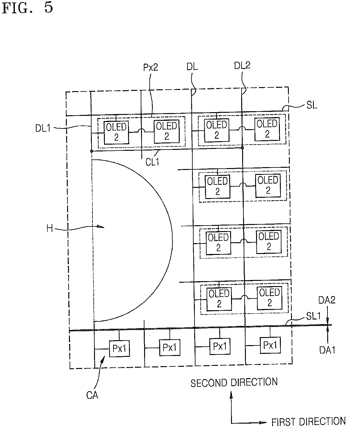
- FIG. 5 is a magnified plan view of an example of the portion A of FIG. 2
- FIG. 6 is a magnified plan view of another example of the portion A of FIG. 2
- FIG. 7 is a circuit diagram of an example of an equivalent circuit of a second pixel Px2 included in the second display region DA2 of the display unit 200 of FIG. 2
- FIG. 8 is a cross-sectional view taken along the line II-II of FIG. 1 .
- the display region DA may include the first display region DA1 and the second display region DA2 having different resolutions.
- the first display region DA1 may be defined as a region where the first pixels Px1 are consecutively arranged in a first direction that is parallel to the plurality of scan lines SL, and in a second direction that is parallel to the plurality of data lines DL, and are arranged among the crossing regions CA between the plurality of data lines DL and the plurality of scan lines SL.
- the second display region DA2 may be defined as the remaining region.
- the first display region DA1 may be defined as a region where the first pixel circuits C1 of FIG. 3 are consecutively arranged in the first direction and in the second direction among the crossing regions CA between the plurality of data lines DL and the plurality of scan lines SL.
- the first display region DA1 and the second display region DA2 may be defined by a first scan line SL1, which is connected to all of the first pixel circuits C1 of FIG. 3 at the crossing regions CA between the first scan line SL1 and the plurality of data lines DL, and which is closest to the at least one through portion H.
- the crossing regions CA between the first scan line SL1 and the plurality of data lines DL may be, or may be at, an edge of the first display region DA1, and accordingly the first display region DA1 and the second display region DA2 may be divided by the first scan line SL1.
- first display region DA1 and the second display region DA2 may be divided in various forms.
- crossing regions CA in which the first pixels Px1 are consecutively arranged in the first direction may also extend in the second direction around the through portion H.
- a boundary between the first display region DA1 and the second display region DA2 may have a step shape in a plan view, and the first display region DA1 may have a shape that surrounds a portion of the through portion H.
- the resolution of the second display region DA2 may be lower than that of the first display region DA1.
- the second display region DA2 includes a plurality of second pixels Px2, and each of the plurality of second pixels Px2 may include one second pixel circuit C2 (see FIG. 7 ), and may include a plurality of second light-emitting devices OLED2. Referring to FIGS. 5 and 6 , more second pixels Px2 may be arranged between the first scan line SL1 and the through portion H.
- the second display region DA2 some of the plurality of data lines DL are not directly connected to the second pixels Px2.
- no second pixel circuits C2 of FIG. 7 are in some of the crossing regions CA between the plurality of data lines DL and the plurality of scan lines SL. Accordingly, the number of second pixel circuits C2 of FIG. 7 per unit area is smaller than the number of first pixel circuits C1 of FIG. 3 per unit area.
- the first light-emitting devices OLED1 of FIG. 4 included in the first display region DA1 and in the second light-emitting devices OLED2 included in the second display region DA2 may be formed equally.
- the number of first light-emitting devices OLED1 of FIG. 3 per unit area may be equal to that of second light-emitting devices OLED2, and thus the number of first light-emitting devices OLED1 of FIG. 3 driven by one first pixel circuit C1 of FIG. 3 may be different from that of second light-emitting devices OLED2 driven by one second pixel circuit C2 of FIG. 7 .
- FIG. 5 illustrates an example in which one second pixel Px2 includes two second light-emitting devices OLED2.
- a first pixel Px1 includes one first light-emitting device OLED1 of FIG. 3 .
- the number of first light-emitting devices OLED1 of FIG. 3 driven by one first pixel circuit C1 of FIG. 3 is less than that of second light-emitting devices OLED2 driven by one second pixel circuit C2 of FIG. 7 , and consequently, within identically sized areas, the number of second pixels Px2 is less than that of first pixels Px1.
- resolution of the second display region DA2 may be lower than that of the first display region DA1.
- one scan signal may be used for two scan lines SL.
- Two or more second light-emitting devices OLED2 connected to one second pixel circuit C2 of FIG. 7 may be simultaneously driven. This will be described later in more detail with reference to FIGS. 7 and 8 .
- the plurality of data lines DL may include a first data line DL1 disconnected by at least one through portion H, and positioned within the second display region DA2, and may also include a second data line DL2 continuously extending over the first display region DA1 and the second display region DA2.
- FIGS. 5 and 6 illustrate one first data line DL1 and one second data line DL2 for convenience of explanation, it should be understood that a plurality of first data lines DL1 and/or a plurality of second data lines DL2 may be included.
- the first data line DL1 is connected to a second pixel Px2.
- the second data line DL2 may be connected to first pixels Px1 within the first display region DA1, and might not be connected to any second pixel Px2 within the second display region DA2.
- the first data line DL1 may be electrically connected to the second data line DL2 by a first connection line CL1. Accordingly, the data signal applied to the second data line DL2 may be equally applied to the first data line DL1, and the second pixel Px2 connected to the first data line DL1 may be normally driven.
- the first connection line CL1 may be on the same layer as the gate electrodes G1 and G2 of FIG. 4 , the same layer as the source and drain electrodes S1, S2, D1, and D2 of FIG. 4 , or the same layer as the second electrode CE2 of the storage capacitor Cst. Accordingly, because an additional process for forming the first connection line CL1 is not necessary, and because the pre-existing second data line DL2 is used as a passage for avoiding the through portion H, the area of the non-display region NDA' of FIG. 8 around the through portion H may be reduced or minimized, and manufacturing efficiency of the display apparatus 1 may improve.
- the first connection line CL1 may cross over the display region DA, or may have a length necessary for connecting the first data line DL1 to the second data line DL2.
- the second data line DL2 may also elongate in the second direction, or may have only sufficient length for connection with the first connection line CL1.
- FIG. 7 illustrates an equivalent circuit of a second pixel Px2 of FIG. 5
- FIG. 8 illustrates a schematic cross-section of the second pixel Px2 of FIG. 5
- FIGS. 5 , 7 , and 8 illustrate, for convenience of explanation, an example in which one second pixel Px2 includes two second light-emitting devices OLED2, embodiments of the present invention are not limited thereto, and one second pixel Px2 may include three or more second light-emitting devices OLED2 that may be simultaneously driven.
- the second pixel circuit C2 may be the same as the first pixel circuit C1 of FIG. 3 .
- the second pixel circuit C2 may include a driving thin film transistor T1', a switching thin film transistor T2', a compensating thin film transistor T3', a first initializing thin film transistor T4', a first light-emission control thin film transistor T5', a second light-emission control thin film transistor T6', a second initializing thin film transistor T7', and at least one storage capacitor Cst'.
- the driving thin film transistor T1' may be electrically connected to the second light-emitting devices OLED2 via the second light-emission control thin film transistor T6' to supply a driving current.
- Pixel electrodes 221' (see FIG. 8 ) of the second light-emitting devices OLED2 may be connected to each other.
- the magnitude of the driving current flowing in the second pixel circuit C2 may be different from that of the driving current flowing in the first pixel circuit C1 of FIG. 3 .
- a driving current that is greater than the driving current flowing in the first pixel circuit C1 of FIG. 3 may flow in the second pixel circuit C2.
- channels of the plurality of thin film transistors T1'-T7' included in the second pixel circuit C2 may be wider than those of the plurality of thin film transistor T1-T7 included in the first pixel circuit C1 of FIG. 3 .
- the channels of the plurality of thin film transistors T1'-T7' included in the second pixel circuit C2 may be shorter than those of the plurality of thin film transistor T1-T7 included in the first pixel circuit C1 of FIG. 3 .
- the channels of the plurality of thin film transistors T1'-T7' included in the second pixel circuit C2 may include a material having a greater charge mobility than a material used to form the channels of the plurality of thin film transistor T1-T7 included in the first pixel circuit C1 of FIG. 3 .
- the gate insulating layer 203 of FIG. 4 positioned on the channels of the plurality of thin film transistors T1'-T7' included in the second pixel circuit C2 may be thinner than that positioned on the channels of the plurality of thin film transistor T1-T7 of FIG. 3 included in the first pixel circuit C1 of FIG. 3 .
- FIG. 8 illustrates a second pixel circuit C2 including only the driving thin film transistor T1', the switching thin film transistor T2', and the storage capacitor Cst' for convenience of explanation.
- the driving thin film transistor T1', the switching thin film transistor T2', and the storage capacitor Cst' may be the same as the driving thin film transistor T1, the switching thin film transistor T2, and the storage capacitor Cst of FIG. 4 , respectively.
- a larger current may flow in a channel of the driving thin film transistor T1' than the current flowing in the channel of the driving thin film transistor T1 of FIG. 4 .
- Each of the two second light-emitting devices OLED2 may include the pixel electrode 221', an opposite electrode 223', and an intermediate layer 222' between the pixel electrode 221' and the opposite electrode 223'.
- the pixel electrodes 221' of the two second light-emitting devices OLED2 may be electrically connected to each other so that the two second light-emitting devices OLED2 may be simultaneously driven by the single second pixel circuit C2.
- the pixel electrodes 221' of the two second light-emitting devices OLED2 may be integrally formed with each other.
- the pixel electrodes 221' of the two second light-emitting devices OLED2 may be electrically connected to each other by an additional line.
- the additional line may be formed at the same layer as the active layers A1 and A2, the gate electrodes G1 and G2, the source and drain electrodes S1, S2, D1, and D2, or the second electrode CE2 of the storage capacitor Cst of FIG. 4 .
- the intermediate layers 222' of the two second light-emitting devices OLED2 that are simultaneously driven may emit light having the same color. Accordingly, the second pixel Px2 may emit red light, green light, blue light, or white light, for example.
- a space between the through portion H and the display region DA is the non-display area NDA'.
- the non-display region NDA' may surround a through portion H.
- the thin film encapsulation layer 300 may extend up to the non-display region NDA'.
- the display apparatus 1 may further include a dam unit D' surrounding the through portion H, in the non-display region NDA'. Because the dam unit D' is the same as the dam unit D of FIG. 4 , the dam unit D' may prevent the organic layer 320 of the thin film encapsulation layer 300 from flowing toward the through portion H.
- the organic layer 320 faces or contacts a lateral surface of the dam unit D' facing the display region DA from among lateral surfaces of the dam unit D', and thus the organic layer 320 is prevented from moving toward, or into, the through portion H.
- the inorganic layers 310 and 330 may cover the dam unit D', and ends of the inorganic layers 310 and 330 may be closer to the through portion H than to the dam unit D'. At least one of the inorganic layers 310 and 330 may contact a lateral surface S of the substrate 100 that is exposed by the through portion H. Accordingly, in the non-display region NDA', edges of the inorganic layers 310 and 330 may be peeled off, and thus encapsulation characteristics of the thin film encapsulation layer 300 may be prevented from being weakened or removed.
- FIG. 9 is a magnified plan view of another example of the portion A of FIG. 2 .
- the plurality of data lines DL may include a first data line DL1 disconnected by at least one through portion H, and positioned within the second display region DA2, may also include a second data line DL2 continuously extending over the first display region DA1 and the second display region DA2, and may also include a third data line DL3 aligned with the first data line DL1 and disconnected from the first data line DL1 by the at least one through portion H.
- FIG. 9 illustrates one first data line DL1, one second data line DL2, and one third data line DL3 for convenience of explanation, it should be understood that a plurality of first data lines DL1, a plurality of second data lines DL2, and a plurality of third data lines DL3 may be included.
- the first data line DL1 is connected to a second pixel Px2.
- the second data line DL2 may be connected to first pixels Px1 within the first display region DA1, and might not be connected to any second pixel Px2 within the second display region DA2.
- a first connection line CL1 may electrically connect the first data line DL1 to the second data line DL2, and a second connection line CL2 may electrically connect the second data line DL2 to the third data line DL3. Accordingly, the data signal applied to the third data line DL3 may be equally applied to the first data line DL1, and the second pixel Px2 connected to the first data line DL1 may normally emit light.
- the first connection line CL1 and the second connection line CL2 may be formed at the same layer as the gate electrodes G1 and G2, the source and drain electrodes S1, S2, D1, and D2, or the second electrode CE2 of the storage capacitor Cst of FIG. 4 .
- the second data line DL2 may be cut off (e.g., may terminate) at a boundary between the first display region DA1 and the second display region DA2 (e.g., at a cut point CP) to prevent a short-circuit between the second data line DL2 and the third data line DL3.
- the cutting off of second data line DL2 at the boundary between the first display region DA1 and the second display region DA2 does not create any problems. Because a portion of the second data line DL2 to which no second data signals are applied due to the cutting is used as a passage for avoiding the through portion H, the area of the non-display region NDA' of FIG. 8 around the through portion H may be reduced or minimized, and manufacturing efficiency of the display apparatus 1 may improve.
- the second pixels Px2 each include a plurality of second light-emitting devices OLED2 that are simultaneously driven and that emit light having the same color, resolution of the second display region DA2 may be lower than that of the first display region DA1.
- FIGS. 10 and 11 are plan views illustrating examples in which light-emitting devices are arranged within the display region DA of the display apparatus 1 of FIG. 1 .
- FIG. 10 illustrates an example in which the light-emitting devices are arranged in a pentile manner.
- the arrangement manner of the light-emitting devices may be equally applied to the first display region DA1 of FIG. 1 and the second display region DA2 of FIG. 1 .
- one light-emitting device may be connected to one first pixel circuit C1 of FIG. 3 to form one first pixel Px1.
- a plurality of light-emitting devices may be connected to one second pixel circuit C2 of FIG. 7 .
- the plurality of light-emitting devices connected to the single second pixel circuit C2 of FIG. 7 may emit light having the same color.
- the light-emitting devices when the light-emitting devices are arranged in a pentile manner, four green (G) light-emitting devices may be simultaneously driven by one second pixel circuit C2 of FIG. 7 , two red (R) light-emitting devices may be simultaneously driven by another second pixel circuit C2 of FIG. 7 , and two blue (B) light-emitting devices may be simultaneously driven by another second pixel circuit C2 of FIG. 7 . Accordingly, the 8 light-emitting devices may be driven by the three second pixel circuits C2 of FIG. 7 .
- embodiments of the present invention are not limited thereto, and the number of light-emitting devices simultaneously driven by one second pixel circuit C2 of FIG. 7 may vary in other embodiments.
- two green light-emitting devices may be simultaneously driven by one second pixel circuit C2 of FIG. 7 , while the other two green light-emitting devices may be simultaneously driven by another second pixel circuit C2.
- the 8 light-emitting devices may be driven by four second pixel circuits C2 of FIG. 7 .
- FIG. 11 illustrates an example in which the light-emitting devices are arranged in a stripe manner.
- two light-emitting devices that emit red light are connected to each other
- two light-emitting devices that emit blue light are connected to each other
- two light-emitting devices that emit green light are connected to each other.
- 6 light-emitting devices are driven by three second pixel circuits C2 of FIG. 7 .
- embodiments of the present invention are not limited thereto, and the number of light-emitting devices simultaneously driven by one second pixel circuit C2 of FIG. 7 may vary.
- the light-emitting devices when the light-emitting devices are arranged in the same stripe manner, four light-emitting devices that emit red light may be connected to one another, four light-emitting devices that emit blue light may be connected to one another, and four light-emitting devices that emit green light may be connected to one another.
- FIG. 12 is a schematic plan view of a display apparatus 2, which is a modification of the display apparatus 1 of FIG. 1 .
- FIG. 12 A description of FIG. 12 that is the same as given above with reference to FIG. 1 will not be repeated herein, and only differences between the display apparatuses 1 and 2 respectively of FIGS. 1 and 12 will be described.
- the display apparatus 2 of FIG. 12 may include the display unit 200 on the substrate 100, and the display unit 200 may include the display region DA including the first display region DA1 and the second display region DA2 having different resolutions.
- the second display region DA2 at least one through portion H penetrating through the substrate 100 and the display unit 200 may be formed. Because some of the data lines in the second display region DA2 are not directly connected to any second pixel circuit C2 of FIG. 7 to be used as a passage for avoiding the through portion H, resolution of the second display region DA2 may be lower than that of the first display region DA1.
- the second display region DA2 may have a reduced or minimized area that surrounds the through portion H.
- the areas of the second display region DA2 may vary according to the number of data lines disconnected by the through portion H. Accordingly, the display apparatus 2 of FIG. 12 may include the high-resolution first display region DA1 having an increased area.
- a camera, a sensor, an LED, and the like may be mounted in the at least one through portion H.
- the camera, the sensor, the LED, and the like are arranged in the through portion H formed in the second display region DA2, the display region DA of the display apparatus 2 that displays an image may widen.
- a through portion H in which a camera and the like may be mounted is positioned within a display region of a display apparatus, and thus the display region for displaying an image may widen.
- the display apparatus may have a reduced non-display region around the through portion H and may provide improved manufacturing efficiency.
Landscapes
- Engineering & Computer Science (AREA)
- Physics & Mathematics (AREA)
- Computer Hardware Design (AREA)
- General Physics & Mathematics (AREA)
- Theoretical Computer Science (AREA)
- Microelectronics & Electronic Packaging (AREA)
- Geometry (AREA)
- Optics & Photonics (AREA)
- Electroluminescent Light Sources (AREA)
- Devices For Indicating Variable Information By Combining Individual Elements (AREA)
- Preparation Of Compounds By Using Micro-Organisms (AREA)
- Measuring Pulse, Heart Rate, Blood Pressure Or Blood Flow (AREA)
- Compounds Of Unknown Constitution (AREA)
Abstract

Description
- One or more embodiments of the invention relate to a display apparatus.
- Applications of conventional display devices have diversified. Also, due to their relatively small thickness and light weight, the application range thereof has increased. In particular, flat panel display devices have been recently researched and manufactured.
- Because display devices may be formed to be flat, various methods may be used to design display devices of different shapes, and the number of functions that may be applied or linked to the display devices has increased.
- One or more embodiments of the invention include a display apparatus including at least one through portion in a display region.
- Additional aspects of the invention will be set forth in part in the description that follows and, in part, will be apparent from the description, or may be learned by practice of the presented embodiments.
- According to one or more embodiments of the invention, a display apparatus includes a substrate, a display unit on the substrate and including a display region including a first display region having therein a plurality of first pixel circuits, and a plurality of first light-emitting devices configured to be driven by the plurality of first pixel circuits, and a second display region having therein a plurality of second pixel circuits, and a plurality of second light-emitting devices configured to be driven by the plurality of second pixel circuits, a plurality of scan lines crossing the display region in a first direction, and a plurality of data lines crossing the display region in a second direction that is different from the first direction, wherein resolutions of the first and second display regions are different, wherein a total number of the first light-emitting devices driven by one of the first pixel circuits is different from a total number of the second light-emitting devices driven by one of the second pixel circuits, and wherein the display unit and the substrate collectively define at least one through portion in the second display region.
- The total number of the first light-emitting devices driven by the one of the first pixel circuits may be less than the total number of the second light-emitting devices driven by the one of the second pixel circuits.
- A number of the first light-emitting device per unit area may be equal to a number of the second light-emitting devices per unit area.
- The plurality of data lines may include a first data line disconnected at the at least one through portion in the second display region, and directly connected to the one of the second pixel circuits, and a second data line continuously extending over the first display region and the second display region, electrically connected to the first data line by a first connection line, and directly connected to the one of the first pixel circuits.
- The plurality of data lines may further include a third data line aligned with the first data line, and separated from the first data line by the at least one through portion, the second data line and the third data line may be electrically connected to each other by a second connection line, and a same data signal may be applied to the first data line and the third data line.
- The second data line may terminate at a boundary between the first display region and the second display region.
- Each of the second pixel circuits may include a thin film transistor including an active layer, a gate electrode, a source electrode, and a drain electrode, and a storage capacitor including a second electrode, and a first electrode that includes the gate electrode of the thin film transistor, and the first connection line and the second connection line may be at a same layer as the gate electrode, the source electrode, the drain electrode, or the second electrode.
- Each of the plurality of second light-emitting devices may include a pixel electrode, and an intermediate layer including an organic emission layer on the pixel electrode, at least two of the second light-emitting devices may be simultaneously driven by one second pixel circuit, and the pixel electrodes of the at least two second light-emitting devices may be electrically connected to each other.
- The intermediate layers of the at least two second light-emitting devices may be configured to emit light having a same color.
- The first pixel circuit may include a first thin film transistor, the second pixel circuit may include a second thin film transistor, and a magnitude of a driving current of the first thin film transistor may be different from a magnitude of a driving current of the second thin film transistor.
- The display apparatus may further include a thin film encapsulation layer that encapsulates the display unit, and that includes at least one organic layer and at least one inorganic layer, the display unit may include a non-display region at an edge of the at least one through portion to surround the at least one through portion, and the thin film encapsulation layer may extend to the non-display region.
- The display apparatus may further include a dam unit that surrounds the at least one through portion at the non-display region, an end of the organic layer may face or may contact a lateral surface of the dam unit facing the display region, the inorganic layer may cover the dam unit, and an end of the inorganic layer may be closer to the at least one through portion than to the dam unit.
- The inorganic layer may contact a lateral surface of the substrate exposed by the at least one through portion.
- According to one or more embodiments of the invention, a display apparatus includes a substrate, a display unit on the substrate, the substrate and the display unit collectively defining at least one through portion, and a thin film encapsulation layer that encapsulates the display unit, and that includes an organic layer and an inorganic layer, wherein the display unit includes a display region including first and second display regions having different resolutions, a non-display region at an edge of, and surrounding, the at least one through portion, and a dam unit within the non-display region and surrounding the at least one through portion, wherein the organic layer faces or contacts a lateral surface of the dam unit that faces the display region, and wherein the inorganic layer covers the dam unit, and contacts a lateral surface of the substrate exposed by the at least one through portion.
- The display apparatus may further include a plurality of first pixel circuits, a plurality of first light-emitting devices configured to be driven by the plurality of first pixel circuits in the first display region, a plurality of second pixel circuits, and a plurality of second light-emitting devices configured to be driven by the plurality of second pixel circuits in the second display region, and a number of first light-emitting devices driven by one of the first pixel circuits may be less than a number of second light-emitting devices driven by one of the second pixel circuits.
- The at least one through portion may be in the second display region.
- The display unit may further include a plurality of scan lines crossing the display region in a first direction, and a plurality of data lines crossing the display region in a second direction that is different from the first direction, the plurality of data lines may include a first data line in the second display region and disconnected at the at least one through portion, and a second data line continuously extending over the first display region and the second display region, and the first data line and the second data line may be electrically connected to each other by a first connection line.
- The first data line may be directly connected only to the one of the second pixel circuits, and the second data line may be directly connected only to the one of the first pixel circuits.
- The plurality of data lines may further include a third data line aligned with the first data line, and separated from the first data line by the at least one through portion, the second data line and the third data line may be electrically connected to each other by a second connection line, and the second data line may terminate at a boundary between the first display region and the second display region.
- Each of the plurality of second pixel circuits may include a thin film transistor including an active layer, a gate electrode, a source electrode, and a drain electrode, and the first connection line and the second connection line may be at a same layer as the active layer, the gate electrode, the source electrode, or the drain electrode.
- Each of the plurality of second light-emitting devices may include a pixel electrode, and an intermediate layer including an organic emission layer on the pixel electrode, at least two of the plurality of second light-emitting devices may be simultaneously driven by one second pixel circuit, and the pixel electrodes of the at least two second light-emitting devices may be electrically connected to each other.
- The intermediate layers of the at least two second light-emitting devices may be configured to emit light having a same color.
- The first pixel circuit may include a first thin film transistor, the second pixel circuit may include a second thin film transistor, and a magnitude of a driving current of the first thin film transistor may be different from a magnitude of a driving current of the second thin film transistor.
- At least some of the above and other features of the invention are set out in the claims.
- These and/or other aspects will become apparent, and will be more readily appreciated, from the following description of the embodiments of the invention, taken in conjunction with the accompanying drawings, in which:
-
FIG. 1 is a schematic plan view of a display apparatus according to an embodiment of the present invention; -
FIG. 2 is a schematic plan view of a display unit of the display apparatus ofFIG. 1 ; -
FIG. 3 is a circuit diagram of an example of an equivalent circuit of a first pixel included in a first display region of the display unit ofFIG. 2 ; -
FIG. 4 is a cross-sectional view taken along the line I-I ofFIG. 1 ; -
FIG. 5 is a magnified plan view of an example of the portion A ofFIG. 2 ; -
FIG. 6 is a magnified plan view of another example of the portion A ofFIG. 2 ; -
FIG. 7 is a circuit diagram of an example of an equivalent circuit of a second pixel included in a second display region of the display unit ofFIG. 2 ; -
FIG. 8 is a cross-sectional view taken along the line II-II ofFIG. 1 ; -
FIG. 9 is a magnified plan view of another example of the portion A ofFIG. 2 ; -
FIG. 10 is a plan view illustrating an example in which light-emitting devices are arranged within a display region of the display apparatus ofFIG. 1 ; -
FIG. 11 is a plan view illustrating another example in which light-emitting devices are arranged within a display region of the display apparatus ofFIG. 1 ; and -
FIG. 12 is a schematic plan view of a display apparatus, which is a modification of the display apparatus ofFIG. 1 . - Features of the inventive concept and methods of accomplishing the same may be understood more readily by reference to the following detailed description of embodiments thereafter and the accompanying drawings. Hereinafter, example embodiments will be described in more detail with reference to the accompanying drawings, in which like reference numbers refer to like elements throughout. The present invention, however, may be embodied in various different forms, and should not be construed as being limited to only the illustrated embodiments herein. Rather, these embodiments are provided as examples so that this disclosure will be thorough and complete, and will fully convey the aspects and features of the present invention to those skilled in the art. Accordingly, processes, elements, and techniques that are not necessary to those having ordinary skill in the art for a complete understanding of the aspects and features of the present invention may not be described. Unless otherwise noted, like reference numerals denote like elements throughout the attached drawings and the written description, and thus, descriptions thereof will not be repeated. In the drawings, the relative sizes of elements, layers, and regions may be exaggerated for clarity.
- It will be understood that, although the terms "first," "second," "third," etc., may be used herein to describe various elements, components, regions, layers and/or sections, these elements, components, regions, layers and/or sections should not be limited by these terms. These terms are used to distinguish one element, component, region, layer or section from another element, component, region, layer or section. Thus, a first element, component, region, layer or section described below could be termed a second element, component, region, layer or section, without departing from the scope of the present invention.
- Spatially relative terms, such as "beneath," "below," "lower," "under," "above," "upper," and the like, may be used herein for ease of explanation to describe one element or feature's relationship to another element(s) or feature(s) as illustrated in the figures. It will be understood that the spatially relative terms are intended to encompass different orientations of the device in use or in operation, in addition to the orientation depicted in the figures. For example, if the device in the figures is turned over, elements described as "below" or "beneath" or "under" other elements or features would then be oriented "above" the other elements or features. Thus, the example terms "below" and "under" can encompass both an orientation of above and below. The device may be otherwise oriented (e.g., rotated 90 degrees or at other orientations) and the spatially relative descriptors used herein should be interpreted accordingly.
- It will be understood that when an element, layer, region, or component is referred to as being "on," "connected to," or "coupled to" another element, layer, region, or component, it can be directly on, connected to, or coupled to the other element, layer, region, or component, or one or more intervening elements, layers, regions, or components may be present. In addition, it will also be understood that when an element or layer is referred to as being "between" two elements or layers, it can be the only element or layer between the two elements or layers, or one or more intervening elements or layers may also be present.
- In the following examples, the x-axis, the y-axis and the z-axis are not limited to three axes of a rectangular coordinate system, and may be interpreted in a broader sense. For example, the x-axis, the y-axis, and the z-axis may be perpendicular to one another, or may represent different directions that are not perpendicular to one another.
- The terminology used herein is for the purpose of describing particular embodiments only and is not intended to be limiting of the present invention. As used herein, the singular forms "a," "an," and "the" are intended to include the plural forms as well, unless the context clearly indicates otherwise. It will be further understood that the terms "comprises," "comprising," "includes," and "including," when used in this specification, specify the presence of the stated features, integers, steps, operations, elements, and/or components, but do not preclude the presence or addition of one or more other features, integers, steps, operations, elements, components, and/or groups thereof. As used herein, the term "and/or" includes any and all combinations of one or more of the associated listed items. Expressions such as "at least one of," when preceding a list of elements, modify the entire list of elements and do not modify the individual elements of the list.
- As used herein, the term "substantially," "about," and similar terms are used as terms of approximation and not as terms of degree, and are intended to account for the inherent deviations in measured or calculated values that would be recognized by those of ordinary skill in the art. Further, the use of "may" when describing embodiments of the present invention refers to "one or more embodiments of the present invention." As used herein, the terms "use," "using," and "used" may be considered synonymous with the terms "utilize," "utilizing," and "utilized," respectively. Also, the term "exemplary" is intended to refer to an example or illustration.
- When a certain embodiment may be implemented differently, a specific process order may be performed differently from the described order. For example, two consecutively described processes may be performed substantially at the same time or performed in an order opposite to the described order.
- The electronic or electric devices and/or any other relevant devices or components according to embodiments of the present invention described herein may be implemented utilizing any suitable hardware, firmware (e.g. an application-specific integrated circuit), software, or a combination of software, firmware, and hardware. For example, the various components of these devices may be formed on one integrated circuit (IC) chip or on separate IC chips. Further, the various components of these devices may be implemented on a flexible printed circuit film, a tape carrier package (TCP), a printed circuit board (PCB), or formed on one substrate. Further, the various components of these devices may be a process or thread, running on one or more processors, in one or more computing devices, executing computer program instructions and interacting with other system components for performing the various functionalities described herein. The computer program instructions are stored in a memory which may be implemented in a computing device using a standard memory device, such as, for example, a random access memory (RAM). The computer program instructions may also be stored in other non-transitory computer readable media such as, for example, a CD-ROM, flash drive, or the like. Also, a person of skill in the art should recognize that the functionality of various computing devices may be combined or integrated into a single computing device, or the functionality of a particular computing device may be distributed across one or more other computing devices without departing from the spirit and scope of the exemplary embodiments of the present invention.
- Unless otherwise defined, all terms (including technical and scientific terms) used herein have the same meaning as commonly understood by one of ordinary skill in the art to which the present invention belongs. It will be further understood that terms, such as those defined in commonly used dictionaries, should be interpreted as having a meaning that is consistent with their meaning in the context of the relevant art and/or the present specification, and should not be interpreted in an idealized or overly formal sense, unless expressly so defined herein.
-
FIG. 1 is a schematic plan view of adisplay apparatus 1 according to an embodiment of the present invention, andFIG. 2 is a schematic plan view of adisplay unit 200 of thedisplay apparatus 1 ofFIG. 1 . - Referring to
FIGS. 1 and2 , thedisplay apparatus 1 may include asubstrate 100, thedisplay unit 200 on thesubstrate 100, and at least one through portion H penetrating through thedisplay unit 200 and thesubstrate 100. - The
display unit 200 may include a display region DA where an image is realized, a plurality of scan lines SL that cross the display region DA in a first direction, and a plurality of data lines DL that cross the display region DA in a second direction that is different from the first direction. For example, the first direction and the second direction may be perpendicular to each other. A plurality of pixels Px1 and Px2 may be respectively positioned at crossing regions CA of the plurality of data lines DL and the plurality of scan lines SL. - For example, the plurality of scan lines SL may transmit scan signals, which are received from a first
scan driving unit 20 and from a secondscan driving unit 30, to the plurality of pixels Px1 and Px2. For example, some of the plurality of scan lines SL may receive a scan signal from the firstscan driving unit 20, and the remaining ones of the plurality of scan lines SL may receive a scan signal from the secondscan driving unit 30. The firstscan driving unit 20 and the secondscan driving unit 30 may be synchronized with each other by a synchronized clock signal. - The plurality of data lines DL may receive a data signal from a
data driving unit 10, and may transmit the data signal to the plurality of pixels Px1 and Px2. - A
controller 40 may change an externally-received image signal to an image data signal, and may transmit the image data signal to thedata driving unit 10. Thecontroller 40 may receive a synchronization signal and a clock signal to generate control signals for controlling the firstscan driving unit 20, the secondscan driving unit 30, and thedata driving unit 10, and may respectively transmit the control signals to the firstscan driving unit 20, the secondscan driving unit 30, and thedata driving unit 10. - The display region DA may include a first display region DA1 and a second display region DA2 having different resolutions. The first pixels Px1 may be positioned in the first display region DA1. The second pixels Px2 may be positioned in the second display region DA2. For example, the resolution of the first display region DA1 may be higher than that of the second display region DA2. In other words, in separate identically sized areas of the first and second display regions DA1 and DA2, the number of first pixels Px1 may be higher than that of second pixels Px2.
- The at least one through portion H may be positioned within the second display region DA2. A camera, a sensor, and the like may be mounted in the at least one through portion H. The at least one through portion H may be a space for an extra member for a function of the
display apparatus 1, or for an extra member capable of adding a new function to thedisplay apparatus 1. The second display region DA2 and the at least one through portion H are not limited to the example shown inFIG. 1 . In other words, the second display region DA2 may be at any of various places, such as a center portion or a lower portion of the display region DA, and the second display region DA2 may also be set to have various sizes. The at least one through portion H need not be circular, and may instead have various shapes, such as a triangular or polygonal shape. Further, the shape, size, and location of the at least one through portion H may vary. For example, the at least one through portion H may be adjacent the first display region DA. For example, the second display region DA2 may partially surround the through portion H. Thus, in plan view, the through portion H may extend up to the edge of thesubstrate 100. - Because some of the plurality of data lines DL and the plurality of scan lines SL overlap the at least one through portion H, a disconnection in the data lines DL and the scan lines SL occurs due to the at least one through portion H. Because the plurality of scan lines SL receive the scan signals from both of the first
scan driving unit 20 and the secondscan driving unit 30, which are located on opposite sides of thedisplay unit 200, the plurality of scan lines SL are not affected by the disconnection due to the at least one through portion H. However, when a data line DL is disconnected due to the at least one through portion H, a data signal is not transmitted to the second pixels Px2 located on the side of the at least one through portion H that is opposite thedata driving unit 10, and thus the quality of the second display region DA2 may degrade. - To address this problem, a data line DL that overlaps the through portion H may have a curved shape to avoid the through portion H. However, when the data line DL has the curved shape and is located along an exterior circumference of the through portion H, an additional space may be used to dispose the data line DL having the curved shape around the through portion H. Thus, the area of a non-display region NDA' around the through portion H may increase (e.g., see
FIG. 8 ). - However, according to the present embodiment, because some of the plurality of data lines DL are not directly connected to the second pixels Px2 in the second display region DA2, a data line DL disconnected due to the through portion H may be connected to another data line DL that is not directly connected to the second pixels Px2 by a first connection line CL1 (e.g., see
FIG. 5 ), and may receive a data signal. - Accordingly, because a pre-existing data line DL is used as a passage for avoiding the through portion H, the area of the non-display region NDA' around the through portion H (e.g., see
FIG. 8 ) may be reduced or minimized, and manufacturing efficiency of thedisplay apparatus 1 may improve. This will be described later in more detail with reference toFIG. 5 . -
FIG. 3 is a circuit diagram of an example of an equivalent circuit of a first pixel Px1 included in the first display region DA1 of thedisplay unit 200 ofFIG. 2 , andFIG. 4 is a cross-sectional view taken along the line I-I ofFIG. 1 . - Referring to
FIG. 3 , the first pixel Px1 may include a first pixel circuit C1 and a first light-emitting device OLED1. The first light-emitting device OLED1 may emit red light, green light, blue light, or white light. - For example, the first pixel circuit C1 may include a plurality of thin film transistors T1-T7 and at least one storage capacitor Cst. The first pixel circuit C1 may be electrically connected to the first light-emitting device OLED1. The first light-emitting device OLED1 may receive a driving current via the first pixel circuit C1, and may emit light.
- The plurality of thin film transistors T1-T7 may include a driving thin film transistor T1, a switching thin film transistor T2, a compensating thin film transistor T3, a first initializing thin film transistor T4, a first light-emission control thin film transistor T5, a second light-emission control thin film transistor T6, and a second initializing thin film transistor T7.
- The first pixel circuit C1 may include a
first scan line 14 for transmitting a first scan signal Sn to the switching thin film transistor T2 and to the compensating thin film transistor T3. The first pixel circuit C1 may also include a second scan line 24 for transmitting a second scan signal Sn-1 to the first initializing thin film transistor T4, athird scan line 34 for transmitting a third scan signal Sn+1 to the second initializing thin film transistor T7, a light-emission control line 15 for transmitting a light-emission control signal En to the first light-emission control thin film transistor T5 and to the second light-emission control thin film transistor T6, adata line 16 for transmitting a data signal Dm, a drivingvoltage line 26 for transmitting a first power supply voltage ELVDD, and an initializingvoltage line 22 for transmitting an initializing voltage VINT for initializing the driving thin film transistor T1. - A drain electrode of the driving thin film transistor T1 may be electrically connected to the first light-emitting device OLED1 via the second light-emission control thin film transistor T6. The driving thin film transistor T1 may receive the data signal Dm according to a switching operation of the switching thin film transistor T2, and may supply the driving current to the first light-emitting device OLED1.
- A gate electrode of the switching thin film transistor T2 may be connected to the
first scan line 14. A source electrode of the switching thin film transistor T2 may be connected to thedata line 16. A drain electrode of the switching thin film transistor T2 may be connected to a source electrode of the driving thin film transistor T1, and may also be connected to the drivingvoltage line 26 via the first light-emission control thin film transistor T5. - The switching thin film transistor T2 is configured to be turned on according to the first scan signal Sn received via the
first scan line 14, and is configured to perform a switching operation for transmitting the data signal Dm received from thedata line 16 to the source electrode of the driving thin film transistor T1. - A gate electrode of the compensating thin film transistor T3 may be connected to the
first scan line 14. A source electrode of the compensating thin film transistor T3 may be connected to the drain electrode of the driving thin film transistor T1, and may also be connected to a pixel electrode 221 (seeFIG. 4 ) of the first light-emitting device OLED1 via the second light-emission control thin film transistor T6. A drain electrode of the compensating thin film transistor T3 is connected to a first electrode CE1 (seeFIG. 4 ) of the storage capacitor Cst, a source electrode of the first initializing thin film transistor T4, and the gate electrode of the driving thin film transistor T1. The compensating thin film transistor T3 is configured to be turned on in response to the first scan signal Sn received via thefirst scan line 14, and is configured to connect the gate electrode of the driving thin film transistor T1 to the drain electrode of the driving thin film transistor T1, such that the driving thin film transistor T1 is diode-connected. - A gate electrode of the first initializing thin film transistor T4 may be connected to the second scan line 24. A drain electrode of the first initializing thin film transistor T4 may be connected to the initializing
voltage line 22. The source electrode of the first initializing thin film transistor T4 may be connected to the first electrode CE1 (seeFIG. 4 ) of the storage capacitor Cst, to the drain electrode of the compensating thin film transistor T3, and to the gate electrode of the driving thin film transistor T1. The first initializing thin film transistor T4 may be turned on according to the second scan signal Sn-1 received via the second scan line 24, and may transmit the initializing voltage VINT to the gate electrode of the driving thin film transistor T1 to thereby perform an initialization operation by initializing a voltage of the gate electrode of the driving thin film transistor T1. - A gate electrode of the first light-emission control thin film transistor T5 may be connected to the light-
emission control line 15. A source electrode of the first light-emission control thin film transistor T5 may be connected to the drivingvoltage line 26. A drain electrode of the first light-emission control thin film transistor T5 is connected to the source electrode of the driving thin film transistor T1, and to the drain electrode of the switching thin film transistor T2. - A gate electrode of the second light-emission control thin film transistor T6 may be connected to the light-
emission control line 15. A source electrode of the second light-emission control thin film transistor T6 may be connected to the drain electrode of the driving thin film transistor T1 and to the source electrode of the compensating thin film transistor T3. A drain electrode of the second light-emission control thin film transistor T6 may be electrically connected to the pixel electrode 221 (seeFIG. 4 ) of the first light-emitting device OLED1. The first light-emission control thin film transistor T5 and the second light-emission control thin film transistor T6 are configured to be simultaneously turned on according to the light-emission control signal En received via the light-emission control line 15, and thus the first power supply voltage ELVDD is able to be transmitted to the first light-emitting device OLED1 when the driving current flows in the first light-emitting device OLED1. - A gate electrode of the second initializing thin film transistor T7 may be connected to the
third scan line 34. A source electrode of the second initializing thin film transistor T7 may be connected to the pixel electrode 221 (seeFIG. 4 ) of the first light-emitting device OLED1. A drain electrode of the second initializing thin film transistor T7 may be connected to the initializingvoltage line 22. The second initializing thin film transistor T7 may be turned on according to the third scan signal Sn+1 received via thethird scan line 34, and may initialize thepixel electrode 221 of the first light-emitting device OLED1. - A second electrode CE2 (see
FIG. 4 ) of the storage capacitor Cst may be connected to the drivingvoltage line 26. The first electrode CE1 (seeFIG. 4 ) of the storage capacitor Cst may be connected to the gate electrode of the driving thin film transistor T1, to the drain electrode of the compensating thin film transistor T3, and to the source electrode of the first initializing thin film transistor T4. - An opposite electrode 223 (see
FIG. 4 ) of the first light-emitting device OLED1 may be connected to a second power supply voltage ELVSS. The first light-emitting device OLED1 may receive a driving current from the driving thin film transistor T1, and may emit light. -
FIG. 3 illustrates an example of a circuit that drives the first pixel Px1, and the first light-emitting device OLED1 may be operated by various other circuit structures. - Because
FIG. 4 is a cross-sectional view schematically illustrating a cross-section of the first pixel Px1,FIG. 4 illustrates a first pixel circuit C1 including the driving thin film transistor T1, the switching thin film transistor T2, and the storage capacitor Cst, for convenience of explanation. - Referring to
FIG. 4 , thesubstrate 100 may include various materials. For example, thesubstrate 100 may be formed of a glass material containing SiO2 as a main component. However, the material used to form thesubstrate 100 is not limited thereto, and thesubstrate 100 may be formed of a plastic material. The plastic material may be polyethersulphone (PES), polyacrylate (PAR), polyetherimide (PEI), polyethyelenen napthalate (PEN), polyethyeleneterepthalate (PET), polyphenylene sulfide (PPS), polyallylate, polyimide, polycarbonate (PC), cellulose triacetate (TAC), cellulose acetate propionate (CAP), cyclic olefin polymer, cyclic olefin copolymer, or the like. - A
buffer layer 201 is formed on thesubstrate 100. Thebuffer layer 201 may reduce or prevent infiltration of a foreign material, moisture, or ambient air from below thesubstrate 100, and may provide a flat surface on thesubstrate 100. Thebuffer layer 201 may include an inorganic material (such as oxide or nitride), an organic material, or an organic and inorganic compound, and may be formed as a single layer or as multiple layers of inorganic and organic material. - A first thin film transistor T1 may be a driving thin film transistor, and may include an active layer A1, a gate electrode G1, a source electrode S1, and a drain electrode D1. A second thin film transistor T2 may be a switching thin film transistor, and may include an active layer A2, a gate electrode G2, a source electrode S2, and a drain electrode D2.
- Although
FIG. 4 illustrates an example in which the first thin film transistor T1 and the second thin film transistor T2 are top gate type thin film transistors, in which the gate electrodes G1 and G2 thereof are respectively on the active layers A1 and A2 with agate insulating layer 203 interposed therebetween, embodiments of the present invention are not limited thereto, and the first thin film transistor T1 and the second thin film transistor T2 may be bottom gate type thin film transistors. - The active layers A1 and A2 of the first thin film transistor T1 and the second thin film transistor T2 may include amorphous silicon or polycrystalline silicon. According to another embodiment, the active layers A1 and A2 may include oxide of at least one selected from the group consisting of indium (In), gallium (Ga), stannum (Sn), zirconium (Zr), vanadium (V), hafnium (Hf), cadmium (Cd), germanium (Ge), chromium (Cr), titanium (Ti), and zinc (Zn). The active layers A1 and A2 may include a channel region, and may also include a source region and a drain region doped with impurities.
- The
gate insulating layer 203 may be on the active layers A1 and A2. Thegate insulating layer 203 may include an inorganic material including oxide or nitride. For example, thegate insulating layer 203 may include silicon oxide (SiO2), silicon nitride (SiNx), silicon oxynitride (SiON), aluminum oxide (Al2O3), titanium oxide (TiO2), tantalum oxide (Ta2O5), hafnium oxide (HfO2), zinc oxide (ZnO2), or the like. - The gate electrodes G1 and G2 respectively of the first thin film transistor T1 and the second thin film transistor T2 may be positioned on the
gate insulating layer 203. The gate electrodes G1 and G2 may include a low resistance metal material. For example, the gate electrodes G1 and G2 may include molybdenum (Mo), aluminum (Al), copper (Cu), and titanium (Ti), and may be formed as a single layer or as a multi-layer. - The gate electrode G1 of the first thin film transistor T1 may also form the first electrode CE1 of the storage capacitor Cst.
- A first
interlayer insulating layer 205 on the gate electrodes G1 and G2 may include an inorganic material including oxide or nitride. For example, the firstinterlayer insulating layer 205 may include silicon oxide (SiO2), silicon nitride (SiNx), silicon oxynitride (SiON), aluminum oxide (Al2O3), titanium oxide (TiO2), tantalum oxide (Ta2O5), hafnium oxide (HfO2), zinc oxide (ZnO2), or the like. - The second electrode CE2 of the storage capacitor Cst is positioned on the first
interlayer insulating layer 205 to overlap the first electrode CE1. Because the first electrode CE1 is the gate electrode G1 of the first thin film transistor T1, the storage capacitor Cst may be positioned to overlap the first thin film transistor T1. - The second electrode CE2 may include a conductive material including molybdenum (Mo), aluminum (Al), copper (Cu), and titanium (Ti), and may be formed as a multi-layer or as a single layer including the aforementioned materials.
- A second
interlayer insulating layer 207 is positioned on the second electrode CE2, and the source electrodes S1 and S2 and the drain electrodes D1 and D2 respectively of the first thin film transistor T1 and the second thin film transistor T2 are positioned on the secondinterlayer insulating layer 207. - For example, the second
interlayer insulating layer 207 may include silicon oxide (SiOx), silicon nitride (SiNx), silicon oxynitride (SiON), aluminum oxide (Al2O3), titanium oxide (TiO2), tantalum oxide (Ta2O5), hafnium oxide (HfO2), zinc oxide (ZnO2), or the like. - The source electrodes S1 and S2 and the drain electrodes D1 and D2 of the first thin film transistor T1 and the second thin film transistor T2 may include a highly-conductive material. For example, each of the source electrodes S1 and S2 and the drain electrodes D1 and D2 may include a conductive material including molybdenum (Mo), aluminum (Al), copper (Cu), and titanium (Ti), and may be formed as a multi-layer or as a single layer including the aforementioned materials. For example, each of the source electrodes S1 and S2 and the drain electrodes D1 and D2 may be formed as a multi-layer of Ti/Al/Ti. A data line DL may be formed on the same layer as a layer on which the source electrodes S1 and S2 and the drain electrodes D1 and D2 are formed.
- The source electrodes S1 and S2 and the drain electrodes D1 and D2 may respectively contact source regions and drain regions of the active layers A1 and A2 via contact holes.
- A
planarization layer 208 may be positioned on the source electrodes S1 and S2 and the drain electrodes D1 and D2, and the first light-emitting device OLED1 may be positioned on theplanarization layer 208. - The
planarization layer 208 may be a single layer including an organic material layer or including a multi-layer formed by stacking single layers including an organic material. The organic material may include a commercial polymer, such as polymethyl methacrylate (PMMA) or polystyrene (PS), a polymer derivative having a phenol-based group, an acryl-based polymer, an imide-based polymer, an acryl ether-based polymer, an amide-based polymer, a fluorine-based polymer, a p-xylene-based polymer, a vinyl alcohol-based polymer, a blend thereof, or the like. Theplanarization layer 208 may be a stack of an inorganic insulation layer and an organic insulation layer. - The first light-emitting device OLED1 may include the
pixel electrode 221, theopposite electrode 223, and anintermediate layer 222 between thepixel electrode 221 and theopposite electrode 223. - The
pixel electrode 221 may be electrically connected to the drain electrode D1 of the first thin film transistor T1 via the second light-emission control thin film transistor T6 ofFIG. 3 . Thepixel electrode 221 may have various shapes. For example, thepixel electrode 221 may be patterned to have an island shape. - For example, the
pixel electrode 221 may be a reflection electrode. For example, thepixel electrode 221 may include a reflection layer formed of silver (Ag), magnesium (Mg), aluminum (Al), platinum (Pt), palladium (Pd), gold (Au), nickel (Ni), neodymium (Nd), iridium (Ir), chromium (Cr), or a compound thereof, and may include a transparent or semi-transparent electrode layer on the reflection layer. The transparent or semi-transparent electrode layer may include at least one selected from the group consisting of indium tin oxide (ITO), indium zinc oxide (IZO), zinc oxide (ZnO), indium oxide (In2O3), indium gallium oxide (IGO), and/or aluminum zinc oxide (AZO). - A
pixel defining layer 212 is formed of an insulating material partially located on thepixel electrode 221. Thepixel defining layer 212 may include at least one organic insulating material selected from the group consisting of polyimide, polyamide (PA), acryl resin, benzocyclobutene (BCB) and a phenolic resin, by using a method such as spin coating. Thepixel defining layer 212 exposes an area of thepixel electrode 221. Theintermediate layer 222 including an organic emission layer is positioned on the exposed area of thepixel electrode 221. - The organic emission layer included in the
intermediate layer 222 may include a low molecular organic material or of a high molecular organic material, and theintermediate layer 222 may further include one or more functional layers, such as a hole transport layer (HTL), an hole injection layer (HIL), an electron transport layer (ETL), and/or an electron injection layer (EIL), in addition to the organic emission layer. - The
opposite electrode 223 may be a transparent or semi-transparent electrode, and may include a metal thin film having a small work function, including Li, Ca, LiF/Ca, LiF/Al, Al, Ag, Mg, or a combination thereof. An auxiliary electrode layer or a bus electrode may include a transparent electrode forming material, such as ITO, IZO, ZnO, or In2O3, on the metal thin film. Accordingly, theopposite electrode 223 may transmit light emitted by the organic emission layer included in theintermediate layer 222. In other words, the light emitted by the organic emission layer may travel directly toward theopposite electrode 223, or may be reflected by thepixel electrode 221 and then travel toward theopposite electrode 223. - A thin
film encapsulation layer 300 is on theopposite electrode 223. The thinfilm encapsulation layer 300 may entirely cover thedisplay unit 200 to prevent external oxygen and moisture from permeating thedisplay unit 200. - The thin
film encapsulation layer 300 may include at least one organic layer (e.g., an organic layer 320), and may include at least one inorganic layer (e.g.,inorganic layers 310 and 330). Theorganic layer 320 and theinorganic layers film encapsulation layer 300 includes the twoinorganic layers organic layer 320 inFIG. 4 , embodiments of the present invention are not limited thereto. In other words, the thinfilm encapsulation layer 300 may further include a plurality of additional inorganic layers and a plurality of additional organic layers that are alternately stacked one on another, and the number of inorganic layers stacked and the number of organic layers stacked are not limited. - The
inorganic layers - The
organic layer 320 may planarize steps caused by thepixel defining layer 212, and may reduce stresses generated on theinorganic layers organic layer 320 may include PMMA, PC, PS, acryl-based resin, epoxy-based resin, polyimide, and/or polyethylene. - The
inorganic layers organic layer 320. Thus, theinorganic layers organic layer 320, and accordingly, permeation of external oxygen or moisture may be effectively prevented. - The
display apparatus 1 may further include a dam unit D surrounding the display region DA, and located in a non-display region NDA around the display region DA. - During formation of the
organic layer 320 of the thinfilm encapsulation layer 300, the dam unit D may block an organic material used to form theorganic layer 320 from flowing toward an edge of thesubstrate 100, thereby preventing formation of an edge tale of theorganic layer 320. The dam unit D may surround the display region DA. - The dam unit D may include the same material used to form at least one of the
planarization layer 208 and thepixel defining layer 212. For example, the dam unit D may include a first layer including the material used to form theplanarization layer 208, and may include a second layer including the material used to form thepixel defining layer 212. However, embodiments of the present invention are not limited thereto, and the dam unit D may include a single layer. A plurality of dam units D may be included. When a plurality of dam units D is included, each of the dam units D has a height increasing in a direction toward the edge of thesubstrate 100. -
FIG. 5 is a magnified plan view of an example of the portion A ofFIG. 2 ,FIG. 6 is a magnified plan view of another example of the portion A ofFIG. 2 ,FIG. 7 is a circuit diagram of an example of an equivalent circuit of a second pixel Px2 included in the second display region DA2 of thedisplay unit 200 ofFIG. 2 , andFIG. 8 is a cross-sectional view taken along the line II-II ofFIG. 1 . - Referring to
FIGS. 2-5 , the display region DA may include the first display region DA1 and the second display region DA2 having different resolutions. - The first display region DA1 may be defined as a region where the first pixels Px1 are consecutively arranged in a first direction that is parallel to the plurality of scan lines SL, and in a second direction that is parallel to the plurality of data lines DL, and are arranged among the crossing regions CA between the plurality of data lines DL and the plurality of scan lines SL. The second display region DA2 may be defined as the remaining region.
- As described above, because each of the first pixels Px1 includes the first pixel circuit C1 of
FIG. 3 and the first light-emitting device OLED1 ofFIG. 3 , the first display region DA1 may be defined as a region where the first pixel circuits C1 ofFIG. 3 are consecutively arranged in the first direction and in the second direction among the crossing regions CA between the plurality of data lines DL and the plurality of scan lines SL. - For example, as shown in
FIG. 2 , when the second display region DA2 covers entirely one side (e.g., an upper side) of the display region DA in a direction parallel to the scan lines SL, the first display region DA1 and the second display region DA2 may be defined by a first scan line SL1, which is connected to all of the first pixel circuits C1 ofFIG. 3 at the crossing regions CA between the first scan line SL1 and the plurality of data lines DL, and which is closest to the at least one through portion H. In other words, the crossing regions CA between the first scan line SL1 and the plurality of data lines DL may be, or may be at, an edge of the first display region DA1, and accordingly the first display region DA1 and the second display region DA2 may be divided by the first scan line SL1. - However, embodiments of the present invention are not limited thereto, and the first display region DA1 and the second display region DA2 may be divided in various forms. As another example, as shown in
FIG. 6 , crossing regions CA in which the first pixels Px1 are consecutively arranged in the first direction may also extend in the second direction around the through portion H. Accordingly, a boundary between the first display region DA1 and the second display region DA2 may have a step shape in a plan view, and the first display region DA1 may have a shape that surrounds a portion of the through portion H. - The resolution of the second display region DA2 may be lower than that of the first display region DA1. The second display region DA2 includes a plurality of second pixels Px2, and each of the plurality of second pixels Px2 may include one second pixel circuit C2 (see
FIG. 7 ), and may include a plurality of second light-emitting devices OLED2. Referring toFIGS. 5 and6 , more second pixels Px2 may be arranged between the first scan line SL1 and the through portion H. - In the second display region DA2, some of the plurality of data lines DL are not directly connected to the second pixels Px2. Thus, no second pixel circuits C2 of
FIG. 7 are in some of the crossing regions CA between the plurality of data lines DL and the plurality of scan lines SL. Accordingly, the number of second pixel circuits C2 ofFIG. 7 per unit area is smaller than the number of first pixel circuits C1 ofFIG. 3 per unit area. - However, the first light-emitting devices OLED1 of
FIG. 4 included in the first display region DA1 and in the second light-emitting devices OLED2 included in the second display region DA2 may be formed equally. In other words, the number of first light-emitting devices OLED1 ofFIG. 3 per unit area may be equal to that of second light-emitting devices OLED2, and thus the number of first light-emitting devices OLED1 ofFIG. 3 driven by one first pixel circuit C1 ofFIG. 3 may be different from that of second light-emitting devices OLED2 driven by one second pixel circuit C2 ofFIG. 7 . - For example,
FIG. 5 illustrates an example in which one second pixel Px2 includes two second light-emitting devices OLED2. However, a first pixel Px1 includes one first light-emitting device OLED1 ofFIG. 3 . Thus, the number of first light-emitting devices OLED1 ofFIG. 3 driven by one first pixel circuit C1 ofFIG. 3 is less than that of second light-emitting devices OLED2 driven by one second pixel circuit C2 ofFIG. 7 , and consequently, within identically sized areas, the number of second pixels Px2 is less than that of first pixels Px1. Thus, resolution of the second display region DA2 may be lower than that of the first display region DA1. In the second display region DA2, one scan signal may be used for two scan lines SL. - Two or more second light-emitting devices OLED2 connected to one second pixel circuit C2 of
FIG. 7 may be simultaneously driven. This will be described later in more detail with reference toFIGS. 7 and8 . - Referring to
FIGS. 5 and6 , the plurality of data lines DL may include a first data line DL1 disconnected by at least one through portion H, and positioned within the second display region DA2, and may also include a second data line DL2 continuously extending over the first display region DA1 and the second display region DA2. AlthoughFIGS. 5 and6 illustrate one first data line DL1 and one second data line DL2 for convenience of explanation, it should be understood that a plurality of first data lines DL1 and/or a plurality of second data lines DL2 may be included. - The first data line DL1 is connected to a second pixel Px2. On the other hand, the second data line DL2 may be connected to first pixels Px1 within the first display region DA1, and might not be connected to any second pixel Px2 within the second display region DA2.
- Within the second display region DA2, the first data line DL1 may be electrically connected to the second data line DL2 by a first connection line CL1. Accordingly, the data signal applied to the second data line DL2 may be equally applied to the first data line DL1, and the second pixel Px2 connected to the first data line DL1 may be normally driven.
- The first connection line CL1 may be on the same layer as the gate electrodes G1 and G2 of
FIG. 4 , the same layer as the source and drain electrodes S1, S2, D1, and D2 ofFIG. 4 , or the same layer as the second electrode CE2 of the storage capacitor Cst. Accordingly, because an additional process for forming the first connection line CL1 is not necessary, and because the pre-existing second data line DL2 is used as a passage for avoiding the through portion H, the area of the non-display region NDA' ofFIG. 8 around the through portion H may be reduced or minimized, and manufacturing efficiency of thedisplay apparatus 1 may improve. - The first connection line CL1 may cross over the display region DA, or may have a length necessary for connecting the first data line DL1 to the second data line DL2. The second data line DL2 may also elongate in the second direction, or may have only sufficient length for connection with the first connection line CL1.
-
FIG. 7 illustrates an equivalent circuit of a second pixel Px2 ofFIG. 5 , andFIG. 8 illustrates a schematic cross-section of the second pixel Px2 ofFIG. 5 . AlthoughFIGS. 5 ,7 , and8 illustrate, for convenience of explanation, an example in which one second pixel Px2 includes two second light-emitting devices OLED2, embodiments of the present invention are not limited thereto, and one second pixel Px2 may include three or more second light-emitting devices OLED2 that may be simultaneously driven. - The second pixel circuit C2 may be the same as the first pixel circuit C1 of
FIG. 3 . In other words, the second pixel circuit C2 may include a driving thin film transistor T1', a switching thin film transistor T2', a compensating thin film transistor T3', a first initializing thin film transistor T4', a first light-emission control thin film transistor T5', a second light-emission control thin film transistor T6', a second initializing thin film transistor T7', and at least one storage capacitor Cst'. - The driving thin film transistor T1' may be electrically connected to the second light-emitting devices OLED2 via the second light-emission control thin film transistor T6' to supply a driving current. Pixel electrodes 221' (see
FIG. 8 ) of the second light-emitting devices OLED2 may be connected to each other. - The magnitude of the driving current flowing in the second pixel circuit C2 may be different from that of the driving current flowing in the first pixel circuit C1 of
FIG. 3 . In other words, because the second pixel circuit C2 needs to simultaneously drive two or more second light-emitting devices OLED2, a driving current that is greater than the driving current flowing in the first pixel circuit C1 ofFIG. 3 may flow in the second pixel circuit C2. - To this end, for example, channels of the plurality of thin film transistors T1'-T7' included in the second pixel circuit C2 may be wider than those of the plurality of thin film transistor T1-T7 included in the first pixel circuit C1 of
FIG. 3 . Alternatively, the channels of the plurality of thin film transistors T1'-T7' included in the second pixel circuit C2 may be shorter than those of the plurality of thin film transistor T1-T7 included in the first pixel circuit C1 ofFIG. 3 . Alternatively, the channels of the plurality of thin film transistors T1'-T7' included in the second pixel circuit C2 may include a material having a greater charge mobility than a material used to form the channels of the plurality of thin film transistor T1-T7 included in the first pixel circuit C1 ofFIG. 3 . Alternatively, thegate insulating layer 203 ofFIG. 4 positioned on the channels of the plurality of thin film transistors T1'-T7' included in the second pixel circuit C2 may be thinner than that positioned on the channels of the plurality of thin film transistor T1-T7 ofFIG. 3 included in the first pixel circuit C1 ofFIG. 3 . -
FIG. 8 illustrates a second pixel circuit C2 including only the driving thin film transistor T1', the switching thin film transistor T2', and the storage capacitor Cst' for convenience of explanation. The driving thin film transistor T1', the switching thin film transistor T2', and the storage capacitor Cst' may be the same as the driving thin film transistor T1, the switching thin film transistor T2, and the storage capacitor Cst ofFIG. 4 , respectively. However, a larger current may flow in a channel of the driving thin film transistor T1' than the current flowing in the channel of the driving thin film transistor T1 ofFIG. 4 . - Each of the two second light-emitting devices OLED2 may include the pixel electrode 221', an opposite electrode 223', and an intermediate layer 222' between the pixel electrode 221' and the opposite electrode 223'.
- The pixel electrodes 221' of the two second light-emitting devices OLED2 may be electrically connected to each other so that the two second light-emitting devices OLED2 may be simultaneously driven by the single second pixel circuit C2. When the two second light-emitting devices OLED2 are adjacent each other, the pixel electrodes 221' of the two second light-emitting devices OLED2 may be integrally formed with each other.
- Alternatively, the pixel electrodes 221' of the two second light-emitting devices OLED2 may be electrically connected to each other by an additional line. The additional line may be formed at the same layer as the active layers A1 and A2, the gate electrodes G1 and G2, the source and drain electrodes S1, S2, D1, and D2, or the second electrode CE2 of the storage capacitor Cst of
FIG. 4 . - The intermediate layers 222' of the two second light-emitting devices OLED2 that are simultaneously driven may emit light having the same color. Accordingly, the second pixel Px2 may emit red light, green light, blue light, or white light, for example.
- A space between the through portion H and the display region DA is the non-display area NDA'. In other words, the non-display region NDA' may surround a through portion H. In this case, the thin
film encapsulation layer 300 may extend up to the non-display region NDA'. - The
display apparatus 1 may further include a dam unit D' surrounding the through portion H, in the non-display region NDA'. Because the dam unit D' is the same as the dam unit D ofFIG. 4 , the dam unit D' may prevent theorganic layer 320 of the thinfilm encapsulation layer 300 from flowing toward the through portion H. - In other words, the
organic layer 320 faces or contacts a lateral surface of the dam unit D' facing the display region DA from among lateral surfaces of the dam unit D', and thus theorganic layer 320 is prevented from moving toward, or into, the through portion H. On the other hand, theinorganic layers inorganic layers inorganic layers substrate 100 that is exposed by the through portion H. Accordingly, in the non-display region NDA', edges of theinorganic layers film encapsulation layer 300 may be prevented from being weakened or removed. -
FIG. 9 is a magnified plan view of another example of the portion A ofFIG. 2 . - Referring to
FIGS. 2 and9 , the plurality of data lines DL may include a first data line DL1 disconnected by at least one through portion H, and positioned within the second display region DA2, may also include a second data line DL2 continuously extending over the first display region DA1 and the second display region DA2, and may also include a third data line DL3 aligned with the first data line DL1 and disconnected from the first data line DL1 by the at least one through portion H. - Although
FIG. 9 illustrates one first data line DL1, one second data line DL2, and one third data line DL3 for convenience of explanation, it should be understood that a plurality of first data lines DL1, a plurality of second data lines DL2, and a plurality of third data lines DL3 may be included. - The first data line DL1 is connected to a second pixel Px2. On the other hand, the second data line DL2 may be connected to first pixels Px1 within the first display region DA1, and might not be connected to any second pixel Px2 within the second display region DA2.
- A first connection line CL1 may electrically connect the first data line DL1 to the second data line DL2, and a second connection line CL2 may electrically connect the second data line DL2 to the third data line DL3. Accordingly, the data signal applied to the third data line DL3 may be equally applied to the first data line DL1, and the second pixel Px2 connected to the first data line DL1 may normally emit light.
- The first connection line CL1 and the second connection line CL2 may be formed at the same layer as the gate electrodes G1 and G2, the source and drain electrodes S1, S2, D1, and D2, or the second electrode CE2 of the storage capacitor Cst of
FIG. 4 . - When the first data line DL1 is electrically connected to the third data line DL3, the second data line DL2 may be cut off (e.g., may terminate) at a boundary between the first display region DA1 and the second display region DA2 (e.g., at a cut point CP) to prevent a short-circuit between the second data line DL2 and the third data line DL3.
- Because the second data line DL2 is not connected to the second pixels Px2 within the second display region DA2, the cutting off of second data line DL2 at the boundary between the first display region DA1 and the second display region DA2 does not create any problems. Because a portion of the second data line DL2 to which no second data signals are applied due to the cutting is used as a passage for avoiding the through portion H, the area of the non-display region NDA' of
FIG. 8 around the through portion H may be reduced or minimized, and manufacturing efficiency of thedisplay apparatus 1 may improve. - Because the second pixels Px2 each include a plurality of second light-emitting devices OLED2 that are simultaneously driven and that emit light having the same color, resolution of the second display region DA2 may be lower than that of the first display region DA1.
-
FIGS. 10 and11 are plan views illustrating examples in which light-emitting devices are arranged within the display region DA of thedisplay apparatus 1 ofFIG. 1 . -
FIG. 10 illustrates an example in which the light-emitting devices are arranged in a pentile manner. The arrangement manner of the light-emitting devices may be equally applied to the first display region DA1 ofFIG. 1 and the second display region DA2 ofFIG. 1 . - Within the first display region DA1 of
FIG. 1 , one light-emitting device may be connected to one first pixel circuit C1 ofFIG. 3 to form one first pixel Px1. On the other hand, within the second display region DA2 ofFIG. 1 , a plurality of light-emitting devices may be connected to one second pixel circuit C2 ofFIG. 7 . The plurality of light-emitting devices connected to the single second pixel circuit C2 ofFIG. 7 may emit light having the same color. - For example, as shown in
FIG. 10 , when the light-emitting devices are arranged in a pentile manner, four green (G) light-emitting devices may be simultaneously driven by one second pixel circuit C2 ofFIG. 7 , two red (R) light-emitting devices may be simultaneously driven by another second pixel circuit C2 ofFIG. 7 , and two blue (B) light-emitting devices may be simultaneously driven by another second pixel circuit C2 ofFIG. 7 . Accordingly, the 8 light-emitting devices may be driven by the three second pixel circuits C2 ofFIG. 7 . However, embodiments of the present invention are not limited thereto, and the number of light-emitting devices simultaneously driven by one second pixel circuit C2 ofFIG. 7 may vary in other embodiments. As another example, in the same pentile structure, two green light-emitting devices may be simultaneously driven by one second pixel circuit C2 ofFIG. 7 , while the other two green light-emitting devices may be simultaneously driven by another second pixel circuit C2. In other words, the 8 light-emitting devices may be driven by four second pixel circuits C2 ofFIG. 7 . -
FIG. 11 illustrates an example in which the light-emitting devices are arranged in a stripe manner. InFIG. 11 , two light-emitting devices that emit red light are connected to each other, two light-emitting devices that emit blue light are connected to each other, and two light-emitting devices that emit green light are connected to each other. In other words, 6 light-emitting devices are driven by three second pixel circuits C2 ofFIG. 7 . However, embodiments of the present invention are not limited thereto, and the number of light-emitting devices simultaneously driven by one second pixel circuit C2 ofFIG. 7 may vary. As another example, when the light-emitting devices are arranged in the same stripe manner, four light-emitting devices that emit red light may be connected to one another, four light-emitting devices that emit blue light may be connected to one another, and four light-emitting devices that emit green light may be connected to one another. -
FIG. 12 is a schematic plan view of adisplay apparatus 2, which is a modification of thedisplay apparatus 1 ofFIG. 1 . - A description of
FIG. 12 that is the same as given above with reference toFIG. 1 will not be repeated herein, and only differences between thedisplay apparatuses FIGS. 1 and12 will be described. - The
display apparatus 2 ofFIG. 12 may include thedisplay unit 200 on thesubstrate 100, and thedisplay unit 200 may include the display region DA including the first display region DA1 and the second display region DA2 having different resolutions. In the second display region DA2, at least one through portion H penetrating through thesubstrate 100 and thedisplay unit 200 may be formed. Because some of the data lines in the second display region DA2 are not directly connected to any second pixel circuit C2 ofFIG. 7 to be used as a passage for avoiding the through portion H, resolution of the second display region DA2 may be lower than that of the first display region DA1. - The second display region DA2 may have a reduced or minimized area that surrounds the through portion H. The areas of the second display region DA2 may vary according to the number of data lines disconnected by the through portion H. Accordingly, the
display apparatus 2 ofFIG. 12 may include the high-resolution first display region DA1 having an increased area. - A camera, a sensor, an LED, and the like may be mounted in the at least one through portion H. In other words, the camera, the sensor, the LED, and the like are arranged in the through portion H formed in the second display region DA2, the display region DA of the
display apparatus 2 that displays an image may widen. - According to embodiments of the present invention, a through portion H in which a camera and the like may be mounted is positioned within a display region of a display apparatus, and thus the display region for displaying an image may widen.
- Moreover, because data lines that extend over the through portion H do not need to have a curved shape in order to avoid the through portion H, the display apparatus may have a reduced non-display region around the through portion H and may provide improved manufacturing efficiency.
- It should be understood that embodiments described herein should be considered in a descriptive sense only and not for purposes of limitation. Descriptions of features or aspects within each embodiment should typically be considered as available for other similar features or aspects in other embodiments.
- While one or more embodiments have been described with reference to the figures, it will be understood by those of ordinary skill in the art that various changes in form and details may be made therein without departing from the scope as defined by the following claims and their equivalents.
Claims (13)
- A display apparatus comprising:a substrate;a display unit on the substrate and comprising:a display region comprising:a first display region having therein a plurality of first pixel circuits, and a plurality of first light-emitting devices configured to be driven by the plurality of first pixel circuits; anda second display region having therein a plurality of second pixel circuits, and a plurality of second light-emitting devices configured to be driven by the plurality of second pixel circuits;a plurality of scan lines crossing the display region in a first direction; anda plurality of data lines crossing the display region in a second direction that is different from the first direction,wherein resolutions of the first and second display regions are different,wherein a total number of the first light-emitting devices driven by one of the first pixel circuits is different from a total number of the second light-emitting devices driven by one of the second pixel circuits, andwherein the display unit and the substrate collectively define at least one through portion in the second display region.
- A display apparatus according to claim 1, wherein the total number of the first light-emitting devices driven by the one of the first pixel circuits is less than the total number of the second light-emitting devices driven by the one of the second pixel circuits.
- A display apparatus according to claim 1 or claim 2, wherein a number of the first light-emitting device per unit area is equal to a number of the second light-emitting devices per unit area.
- A display apparatus according to claim 1, 2 or 3, wherein the plurality of data lines comprise:a first data line disconnected at the at least one through portion in the second display region, and directly connected to the one of the second pixel circuits; anda second data line continuously extending over the first display region and the second display region, electrically connected to the first data line by a first connection line, and directly connected to the one of the first pixel circuits.
- A display apparatus according to claim 4, wherein the plurality of data lines further comprise a third data line aligned with the first data line, and separated from the first data line by the at least one through portion,
wherein the second data line and the third data line are electrically connected to each other by a second connection line, and
wherein a same data signal is applied to the first data line and the third data line. - A display apparatus according to claim 5, wherein the second data line terminates at a boundary between the first display region and the second display region.
- A display apparatus according to claim 5, wherein each of the second pixel circuits comprises:a thin film transistor comprising:an active layer;a gate electrode;a source electrode; anda drain electrode, anda storage capacitor comprising:a second electrode; anda first electrode that comprises the gate electrode of the thin film transistor, andwherein the first connection line and the second connection line are at a same layer as the gate electrode, the source electrode, the drain electrode, or the second electrode.
- A display apparatus according to any preceding claim, wherein each of the plurality of second light-emitting devices comprises:a pixel electrode; andan intermediate layer comprising an organic emission layer on the pixel electrode,wherein at least two of the second light-emitting devices are simultaneously driven by one second pixel circuit, and
wherein the pixel electrodes of the at least two second light-emitting devices are electrically connected to each other. - A display apparatus according to claim 8, wherein the intermediate layers of the at least two second light-emitting devices are configured to emit light having a same color.
- A display apparatus according to any preceding claim, wherein the first pixel circuit comprises a first thin film transistor,
wherein the second pixel circuit comprises a second thin film transistor, and
wherein a magnitude of a driving current of the first thin film transistor is different from a magnitude of a driving current of the second thin film transistor. - A display apparatus according to any preceding claim, further comprising a thin film encapsulation layer that encapsulates the display unit, and that comprises at least one organic layer and at least one inorganic layer,
wherein the display unit comprises a non-display region at an edge of the at least one through portion to surround the at least one through portion, and
wherein the thin film encapsulation layer extends to the non-display region. - A display apparatus according to claim 11, further comprising a dam unit that surrounds the at least one through portion at the non-display region,
wherein an end of the organic layer faces or contacts a lateral surface of the dam unit facing the display region,
wherein the inorganic layer covers the dam unit, and
wherein an end of the inorganic layer is closer to the at least one through portion than to the dam unit. - A display apparatus according to claim 11 or claim 12, wherein the inorganic layer contacts a lateral surface of the substrate exposed by the at least one through portion.
Applications Claiming Priority (1)
| Application Number | Priority Date | Filing Date | Title |
|---|---|---|---|
| KR1020150170668A KR102465379B1 (en) | 2015-12-02 | 2015-12-02 | Display apparatus |
Publications (2)
| Publication Number | Publication Date |
|---|---|
| EP3176772A1 true EP3176772A1 (en) | 2017-06-07 |
| EP3176772B1 EP3176772B1 (en) | 2019-04-17 |
Family
ID=56801452
Family Applications (1)
| Application Number | Title | Priority Date | Filing Date |
|---|---|---|---|
| EP16185776.8A Active EP3176772B1 (en) | 2015-12-02 | 2016-08-25 | Display apparatus |
Country Status (4)
| Country | Link |
|---|---|
| US (3) | US10186191B2 (en) |
| EP (1) | EP3176772B1 (en) |
| KR (1) | KR102465379B1 (en) |
| CN (1) | CN107025875B (en) |
Cited By (15)
| Publication number | Priority date | Publication date | Assignee | Title |
|---|---|---|---|---|
| EP3438732A1 (en) * | 2017-07-31 | 2019-02-06 | Guangdong Oppo Mobile Telecommunications Corp., Ltd | Display panel and electronic device |
| CN110767166A (en) * | 2018-10-31 | 2020-02-07 | 昆山国显光电有限公司 | Display screen and display terminal |
| WO2020041002A1 (en) * | 2018-08-21 | 2020-02-27 | Apple Inc. | Displays with data lines that accommodate openings |
| EP3678188A1 (en) * | 2019-01-04 | 2020-07-08 | Samsung Display Co., Ltd. | Electronic device |
| EP3680888A1 (en) * | 2019-01-10 | 2020-07-15 | Samsung Display Co., Ltd. | Display device having light transmissive regions |
| EP3709367A1 (en) * | 2019-03-12 | 2020-09-16 | Samsung Display Co., Ltd. | Display apparatus and method of manufacturing the same |
| EP3786936A1 (en) * | 2019-08-29 | 2021-03-03 | Samsung Display Co., Ltd. | Method of driving a display panel |
| WO2021167991A1 (en) * | 2020-02-18 | 2021-08-26 | Google Llc | Reducing hole bezel region in displays |
| US20210265430A1 (en) * | 2019-04-04 | 2021-08-26 | Kunshan Go-Visionox Opto-Electronics Co., Ltd. | Oled array substrate, display panel and display device |
| US11127931B2 (en) | 2018-09-28 | 2021-09-21 | Samsung Display Co., Ltd. | Method for manufacturing display panel |
| CN113764460A (en) * | 2020-06-01 | 2021-12-07 | 京东方科技集团股份有限公司 | Display substrate and display device |
| WO2022067965A1 (en) * | 2020-09-30 | 2022-04-07 | 京东方科技集团股份有限公司 | Terminal device, display apparatus, and display panel and manufacturing method therefor |
| EP4024377A4 (en) * | 2019-10-31 | 2022-08-24 | Guangdong Oppo Mobile Telecommunications Corp., Ltd. | Display apparatus and electronic device |
| CN115116393A (en) * | 2020-07-20 | 2022-09-27 | 武汉天马微电子有限公司 | Display panel and display device |
| US11852938B2 (en) | 2018-08-21 | 2023-12-26 | Apple Inc. | Displays with data lines that accommodate openings |
Families Citing this family (149)
| Publication number | Priority date | Publication date | Assignee | Title |
|---|---|---|---|---|
| US11711958B2 (en) * | 2014-09-11 | 2023-07-25 | Boe Technology Group Co., Ltd. | Display panel and display device |
| GB2552090B (en) | 2017-06-29 | 2021-06-16 | Inodyn Newmedia Gmbh | Front-facing camera and maximized display screen of a mobile device |
| KR102483956B1 (en) | 2016-03-31 | 2023-01-03 | 삼성디스플레이 주식회사 | Display device |
| KR102103962B1 (en) | 2016-09-02 | 2020-06-01 | 삼성디스플레이 주식회사 | Display device and manufacturing method thereof |
| CN107808892B (en) | 2016-09-08 | 2020-06-26 | 群创光电股份有限公司 | display screen |
| CN115425052A (en) * | 2017-06-29 | 2022-12-02 | 京东方科技集团股份有限公司 | Display panel and display device |
| JP6723456B2 (en) * | 2017-07-10 | 2020-07-15 | シャープ株式会社 | EL device, EL device manufacturing method, and EL device manufacturing apparatus |
| CN107393458B (en) * | 2017-07-28 | 2019-11-15 | 武汉华星光电半导体显示技术有限公司 | A kind of flexible display panel and device |
| CN107300814B (en) * | 2017-07-31 | 2023-10-13 | Oppo广东移动通信有限公司 | Array substrates, display panels and electronic devices |
| KR102400648B1 (en) * | 2017-08-18 | 2022-05-23 | 삼성디스플레이 주식회사 | Display device and fabricating method of the same |
| WO2019047126A1 (en) * | 2017-09-07 | 2019-03-14 | 华为技术有限公司 | Organic light-emitting display (oled) screen and terminal |
| KR102352312B1 (en) * | 2017-09-29 | 2022-01-19 | 삼성디스플레이 주식회사 | Display device |
| CN108389879B (en) * | 2017-09-30 | 2021-06-15 | 云谷(固安)科技有限公司 | Display and electronic equipment |
| JP7002908B2 (en) * | 2017-10-13 | 2022-01-20 | 株式会社ジャパンディスプレイ | Display device |
| CN112908238B (en) * | 2017-10-27 | 2023-06-23 | 武汉天马微电子有限公司 | A display panel and electronic device |
| CN107845663B (en) * | 2017-10-27 | 2020-12-08 | 武汉天马微电子有限公司 | A display panel and display device |
| KR102483346B1 (en) | 2017-10-30 | 2023-01-02 | 엘지디스플레이 주식회사 | Display Apparatus |
| USD907034S1 (en) | 2017-11-03 | 2021-01-05 | Inodyn Newmedia Gmbh | Mobile electronic device |
| USD898023S1 (en) | 2017-11-03 | 2020-10-06 | Inodyn Newmedia Gmbh | Mobile electronic device |
| KR102444215B1 (en) * | 2017-11-09 | 2022-09-20 | 삼성디스플레이 주식회사 | display device |
| CN108122528A (en) * | 2017-12-13 | 2018-06-05 | 广东欧珀移动通信有限公司 | Display control method and related product |
| KR102550732B1 (en) * | 2017-12-13 | 2023-07-03 | 삼성디스플레이 주식회사 | Display device |
| KR102527993B1 (en) | 2018-01-05 | 2023-05-04 | 삼성디스플레이 주식회사 | Display device and method for manufacturing the same |
| CN110021640B (en) | 2018-01-08 | 2025-02-11 | 三星显示有限公司 | Electroluminescent device |
| KR102572136B1 (en) * | 2018-01-08 | 2023-08-29 | 삼성디스플레이 주식회사 | Electroluminescent device having window |
| KR102413113B1 (en) * | 2018-01-08 | 2022-06-27 | 삼성전자주식회사 | An electronic device comprising a sensor for generating image data using incident light through an opening formed in a display |
| CN110034152B (en) * | 2018-01-12 | 2023-08-04 | 京东方科技集团股份有限公司 | Display panel, manufacturing method thereof, and display device |
| CN108122497B (en) * | 2018-02-02 | 2023-11-14 | 京东方科技集团股份有限公司 | A flexible array substrate, flexible display device and assembly method |
| CN110134182A (en) * | 2018-02-08 | 2019-08-16 | 深圳富泰宏精密工业有限公司 | Portable electronic device and its operating method |
| CN108417605B (en) * | 2018-02-27 | 2020-08-25 | 上海天马微电子有限公司 | Display panel and display device |
| KR102527230B1 (en) * | 2018-03-09 | 2023-05-02 | 삼성디스플레이 주식회사 | Display apparatus |
| JP2019160174A (en) * | 2018-03-16 | 2019-09-19 | シャープ株式会社 | Liquid crystal display panel |
| WO2019186763A1 (en) * | 2018-03-28 | 2019-10-03 | シャープ株式会社 | Display device and method for driving same |
| KR102664717B1 (en) * | 2018-04-13 | 2024-05-10 | 삼성전자 주식회사 | Display comprising a plurality of electric wirings bypassing hole area surrounded by display area, and electronic device comprising the same |
| USD913266S1 (en) | 2018-04-16 | 2021-03-16 | Inodyn Newmedia Gmbh | Smartphone |
| USD911321S1 (en) | 2018-04-16 | 2021-02-23 | Inodyn Newmedia Gmbh | Smartphone |
| USD913267S1 (en) | 2018-04-16 | 2021-03-16 | Inodyn Newmedia Gmbh | Smartphone |
| USD914003S1 (en) | 2018-04-16 | 2021-03-23 | Inodyn Newmedia Gmbh | Smartphone |
| US11201307B2 (en) | 2018-04-17 | 2021-12-14 | Samsung Display Co., Ltd. | Display panel and electronic apparatus including the same |
| CN108417731B (en) * | 2018-05-09 | 2020-02-07 | 京东方科技集团股份有限公司 | Thin film packaging structure, packaging method thereof and OLED display device |
| KR102610254B1 (en) | 2018-05-18 | 2023-12-07 | 삼성디스플레이 주식회사 | Electronic panel and method of manufaturing the same |
| KR102549692B1 (en) | 2018-05-25 | 2023-06-30 | 삼성전자 주식회사 | display device including scan driver for driving display panel in which is formed empty area surrounded by display area |
| CN108732841A (en) * | 2018-05-31 | 2018-11-02 | 厦门天马微电子有限公司 | A kind of display panel and preparation method thereof, display device |
| WO2019240332A1 (en) * | 2018-06-11 | 2019-12-19 | 엘지전자 주식회사 | Mobile terminal |
| KR102592652B1 (en) * | 2018-06-11 | 2023-10-24 | 엘지전자 주식회사 | Mobile terminal |
| KR102580450B1 (en) | 2018-06-22 | 2023-09-20 | 삼성디스플레이 주식회사 | Display module, display panel and method for manufacturing the display panel |
| KR102649144B1 (en) * | 2018-06-25 | 2024-03-21 | 삼성디스플레이 주식회사 | Display apparatus |
| CN108847415B (en) * | 2018-06-29 | 2020-08-11 | 厦门天马微电子有限公司 | Array substrate, gate drive circuit and display panel |
| KR102663905B1 (en) | 2018-07-31 | 2024-05-09 | 삼성디스플레이 주식회사 | Display panel and method of manufacturing the same |
| KR102581242B1 (en) | 2018-08-01 | 2023-09-22 | 삼성디스플레이 주식회사 | Display device |
| KR102699676B1 (en) * | 2018-08-02 | 2024-08-28 | 삼성디스플레이 주식회사 | Display panel |
| KR102548987B1 (en) * | 2018-08-09 | 2023-06-29 | 삼성디스플레이 주식회사 | Display device |
| CN109037298B (en) * | 2018-08-15 | 2021-06-29 | 武汉天马微电子有限公司 | An organic light-emitting display panel and an organic light-emitting display device |
| JP7132032B2 (en) * | 2018-08-23 | 2022-09-06 | 株式会社ジャパンディスプレイ | Display device |
| KR102602191B1 (en) | 2018-08-24 | 2023-11-15 | 삼성디스플레이 주식회사 | Display device |
| CN208848933U (en) * | 2018-08-29 | 2019-05-10 | 昆山国显光电有限公司 | Display panel and display device |
| US10541380B1 (en) | 2018-08-30 | 2020-01-21 | Samsung Display Co., Ltd. | Display device with substrate comprising an opening and adjacent grooves |
| KR102697258B1 (en) * | 2018-09-27 | 2024-08-21 | 삼성디스플레이 주식회사 | Display device |
| KR102612036B1 (en) | 2018-09-27 | 2023-12-11 | 삼성디스플레이 주식회사 | Display panel and electronic device including of the same |
| KR102762691B1 (en) * | 2018-09-28 | 2025-02-06 | 삼성디스플레이 주식회사 | Organic light emitting diode display device |
| CN112133708B (en) * | 2018-09-30 | 2022-07-29 | 厦门天马微电子有限公司 | A display panel, a display device and a manufacturing method of the display panel |
| KR102691772B1 (en) | 2018-10-02 | 2024-08-05 | 삼성디스플레이 주식회사 | Display device |
| KR102602670B1 (en) * | 2018-10-05 | 2023-11-17 | 삼성디스플레이 주식회사 | Display apharatus having input sensing unit |
| KR102697457B1 (en) | 2018-10-11 | 2024-08-22 | 삼성디스플레이 주식회사 | Display panel |
| KR102601689B1 (en) | 2018-10-12 | 2023-11-15 | 삼성디스플레이 주식회사 | Electronic apparatus |
| TWI674572B (en) * | 2018-10-12 | 2019-10-11 | 友達光電股份有限公司 | Non-rectangular display apparatus |
| KR102733114B1 (en) * | 2018-10-31 | 2024-11-21 | 삼성디스플레이 주식회사 | Display device |
| KR102615640B1 (en) * | 2018-10-23 | 2023-12-20 | 삼성디스플레이 주식회사 | Display apparatus |
| US11095762B2 (en) * | 2018-10-23 | 2021-08-17 | International Business Machines Corporation | Display device with camera embedded beneath screen |
| KR102737768B1 (en) | 2018-11-02 | 2024-12-04 | 삼성디스플레이 주식회사 | Display panel and electronic device including the same |
| KR102792465B1 (en) * | 2018-11-15 | 2025-04-07 | 삼성디스플레이 주식회사 | Display device |
| KR102758808B1 (en) * | 2018-12-14 | 2025-01-23 | 엘지디스플레이 주식회사 | Display device |
| KR102648723B1 (en) | 2018-12-31 | 2024-03-18 | 삼성디스플레이 주식회사 | Display device and driving method thereof |
| CN113851600B (en) * | 2019-01-08 | 2023-06-30 | 京东方科技集团股份有限公司 | Display substrate, manufacturing method thereof and display device |
| US11282474B1 (en) * | 2019-01-15 | 2022-03-22 | Rockwell Collins, Inc. | Systems and methods for multi-region displays |
| CN109755282B (en) | 2019-01-15 | 2022-04-15 | 武汉天马微电子有限公司 | Display panel and display device |
| KR102778473B1 (en) | 2019-01-21 | 2025-03-12 | 삼성디스플레이 주식회사 | Display device |
| CN109584794A (en) * | 2019-01-25 | 2019-04-05 | 京东方科技集团股份有限公司 | Display panel and display device |
| KR102770831B1 (en) * | 2019-02-07 | 2025-02-24 | 삼성디스플레이 주식회사 | Display apparatus |
| KR102869845B1 (en) | 2019-03-06 | 2025-10-13 | 삼성디스플레이 주식회사 | Display panel and display apparatus including the same |
| KR102806400B1 (en) | 2019-03-08 | 2025-05-13 | 삼성디스플레이 주식회사 | Display panel |
| KR102808926B1 (en) * | 2019-03-13 | 2025-05-16 | 삼성디스플레이 주식회사 | Flexible display device and augmented reality providing device including the same |
| CN110767834B (en) * | 2019-03-29 | 2020-09-22 | 昆山国显光电有限公司 | Display device and display panel thereof |
| WO2020202247A1 (en) * | 2019-03-29 | 2020-10-08 | シャープ株式会社 | Display device |
| US12022680B2 (en) * | 2019-04-05 | 2024-06-25 | Sharp Kabushiki Kaisha | Display device |
| KR102869843B1 (en) * | 2019-04-11 | 2025-10-13 | 삼성디스플레이 주식회사 | Display apparatus and the manufacturing method thereof |
| KR102724701B1 (en) * | 2019-04-16 | 2024-11-01 | 삼성디스플레이 주식회사 | Method for manufacturing a display apparatus |
| TWI696988B (en) * | 2019-05-02 | 2020-06-21 | 友達光電股份有限公司 | Display panel |
| KR102837682B1 (en) | 2019-05-08 | 2025-07-23 | 삼성디스플레이 주식회사 | Display panel |
| US20200357869A1 (en) * | 2019-05-10 | 2020-11-12 | Samsung Display Co., Ltd. | Display apparatus and method of manufacturing the same |
| KR102806399B1 (en) * | 2019-05-13 | 2025-05-13 | 삼성디스플레이 주식회사 | Display apparatus |
| KR102907359B1 (en) * | 2019-05-31 | 2026-01-02 | 삼성디스플레이 주식회사 | Display panel |
| KR102712664B1 (en) | 2019-06-18 | 2024-10-04 | 삼성디스플레이 주식회사 | Display device and manufacturing method thereof |
| KR102896748B1 (en) | 2019-06-19 | 2025-12-05 | 삼성디스플레이 주식회사 | Display panel |
| KR102936050B1 (en) * | 2019-06-24 | 2026-03-10 | 삼성디스플레이 주식회사 | Display panel and display device having the same |
| KR102914150B1 (en) * | 2019-06-26 | 2026-01-16 | 삼성디스플레이 주식회사 | Display device |
| KR102867421B1 (en) | 2019-07-05 | 2025-10-02 | 삼성디스플레이 주식회사 | Electronic apparatus and method of manufacturing the same |
| KR102845810B1 (en) * | 2019-07-17 | 2025-08-13 | 삼성디스플레이 주식회사 | Display device |
| KR102862554B1 (en) * | 2019-07-31 | 2025-09-22 | 삼성디스플레이 주식회사 | Display device |
| KR102875122B1 (en) | 2019-08-26 | 2025-10-22 | 삼성디스플레이 주식회사 | Display panel and display apparatus comprising the same |
| KR102859922B1 (en) | 2019-09-03 | 2025-09-15 | 삼성디스플레이 주식회사 | Display device |
| CN110543050B (en) * | 2019-09-30 | 2021-11-23 | 上海天马微电子有限公司 | Display panel, display device and compensation method of display device |
| KR102896745B1 (en) | 2019-10-02 | 2025-12-05 | 삼성디스플레이 주식회사 | Display device and electronic product |
| KR102891504B1 (en) * | 2019-10-15 | 2025-11-26 | 삼성디스플레이 주식회사 | Display device |
| KR102919365B1 (en) * | 2019-10-25 | 2026-01-29 | 삼성디스플레이 주식회사 | Display apparatus |
| KR102712663B1 (en) | 2019-10-30 | 2024-10-04 | 삼성디스플레이 주식회사 | Display apparatus |
| CN110783487B (en) * | 2019-10-31 | 2024-11-05 | Oppo广东移动通信有限公司 | Display device and electronic equipment |
| US12165560B2 (en) * | 2019-11-18 | 2024-12-10 | Boe Technology Group Co., Ltd. | Display panel and display device |
| KR102734650B1 (en) * | 2019-12-16 | 2024-11-28 | 삼성디스플레이 주식회사 | Display device and operating method of controller of the same |
| KR20210078003A (en) | 2019-12-18 | 2021-06-28 | 엘지디스플레이 주식회사 | Display device |
| KR102951422B1 (en) * | 2019-12-18 | 2026-04-10 | 삼성디스플레이 주식회사 | Display panel and display apparatus including the same |
| KR102932275B1 (en) * | 2019-12-18 | 2026-02-27 | 삼성디스플레이 주식회사 | Display panel and display device including the same |
| CN211265478U (en) * | 2019-12-20 | 2020-08-14 | 京东方科技集团股份有限公司 | Display substrate and display device |
| KR102865946B1 (en) * | 2019-12-24 | 2025-09-26 | 엘지디스플레이 주식회사 | Organic light emitting display apparatus |
| KR102835926B1 (en) * | 2019-12-24 | 2025-07-17 | 엘지디스플레이 주식회사 | Light emitting display panel |
| KR102756664B1 (en) * | 2019-12-24 | 2025-01-16 | 엘지디스플레이 주식회사 | Organic light emitting display apparatus |
| KR20210082316A (en) | 2019-12-24 | 2021-07-05 | 삼성디스플레이 주식회사 | Display panel and display device including the same |
| KR102933927B1 (en) * | 2019-12-27 | 2026-03-04 | 삼성디스플레이 주식회사 | Display apparatus |
| KR20210085902A (en) * | 2019-12-31 | 2021-07-08 | 엘지디스플레이 주식회사 | Display device |
| KR102943880B1 (en) * | 2019-12-31 | 2026-03-26 | 엘지디스플레이 주식회사 | Light Emitting Display Device |
| CN111161673B (en) * | 2019-12-31 | 2022-08-16 | Oppo广东移动通信有限公司 | Electronic equipment and display screen thereof |
| KR102929425B1 (en) | 2020-01-02 | 2026-02-23 | 삼성디스플레이 주식회사 | Display apparatus |
| KR102852727B1 (en) * | 2020-01-22 | 2025-09-02 | 삼성디스플레이 주식회사 | Display device |
| KR102892883B1 (en) * | 2020-01-28 | 2025-11-28 | 삼성디스플레이 주식회사 | Display apparatus |
| KR102736680B1 (en) | 2020-02-10 | 2024-12-02 | 삼성전자 주식회사 | An electronic device having a structure in which a camera is disposed below a display |
| KR102756813B1 (en) | 2020-03-10 | 2025-01-21 | 삼성디스플레이 주식회사 | Display device and method for driving the same |
| KR102782013B1 (en) * | 2020-04-06 | 2025-03-19 | 삼성디스플레이 주식회사 | Display panel and display apparatus including the same |
| CN115702451A (en) * | 2020-04-09 | 2023-02-14 | Oti照明公司 | Display panel with blind holes for accommodating signals exchanged with underscreen components |
| KR102809348B1 (en) * | 2020-04-13 | 2025-05-19 | 삼성디스플레이 주식회사 | Display device |
| KR102942306B1 (en) | 2020-05-11 | 2026-03-20 | 삼성디스플레이 주식회사 | Display panel and display apparatus including the same |
| JP2023106646A (en) * | 2020-06-15 | 2023-08-02 | ソニーセミコンダクタソリューションズ株式会社 | Image display device and electronic equipment |
| CN111834430B (en) * | 2020-07-09 | 2022-03-08 | 昆山国显光电有限公司 | Display panel and display device |
| US11825709B2 (en) * | 2020-08-11 | 2023-11-21 | Samsung Display Co., Ltd. | Display device |
| KR102853705B1 (en) | 2020-08-14 | 2025-09-02 | 삼성디스플레이 주식회사 | Display apparatus and manufacturing the same |
| KR20220025990A (en) * | 2020-08-24 | 2022-03-04 | 삼성디스플레이 주식회사 | Display Panel and Display Device |
| CN111983843B (en) * | 2020-08-31 | 2022-03-08 | 武汉华星光电技术有限公司 | Display panel and electronic device |
| CN112038380B (en) * | 2020-09-08 | 2023-04-07 | 京东方科技集团股份有限公司 | Display substrate and display device |
| CN212847514U (en) * | 2020-09-30 | 2021-03-30 | 京东方科技集团股份有限公司 | Display panel and display device |
| KR102850821B1 (en) * | 2020-11-04 | 2025-08-26 | 삼성디스플레이 주식회사 | Method for detecting a touch location and display apparatus |
| CN114566519B (en) * | 2020-11-27 | 2026-02-13 | 京东方科技集团股份有限公司 | Display substrate and display device |
| CN112542121B (en) * | 2020-12-03 | 2023-01-31 | Oppo广东移动通信有限公司 | Display structure, display screen and electronic equipment |
| KR102897918B1 (en) * | 2020-12-29 | 2025-12-09 | 삼성디스플레이 주식회사 | Display panel and display apparatus including the same |
| KR102903492B1 (en) * | 2021-02-01 | 2025-12-23 | 삼성디스플레이 주식회사 | Lught emitting display device |
| CN112908247B (en) * | 2021-03-01 | 2022-04-15 | 成都辰显光电有限公司 | Pixel circuit, driving method thereof and display panel |
| KR102946901B1 (en) | 2021-03-26 | 2026-04-01 | 삼성디스플레이 주식회사 | Display apparatus |
| CN115273656B (en) * | 2021-04-30 | 2023-10-24 | 荣耀终端有限公司 | Display panel and display device |
| KR20230049190A (en) * | 2021-10-05 | 2023-04-13 | 삼성디스플레이 주식회사 | Display apparatus |
| US20240122039A1 (en) * | 2022-10-11 | 2024-04-11 | Samsung Display Co., Ltd. | Display device and method for manufacturing the same |
| WO2024250127A1 (en) * | 2023-06-03 | 2024-12-12 | Kunshan Yunyinggu Electronic Technology Co., Ltd. | Display panel and method for rendering subpixels of the display panel |
Citations (4)
| Publication number | Priority date | Publication date | Assignee | Title |
|---|---|---|---|---|
| EP1672411A2 (en) * | 2004-12-14 | 2006-06-21 | Samsung Electronics Co., Ltd. | Thin film transistor panel and liquid crystal display using the same |
| US20090179880A1 (en) * | 2008-01-15 | 2009-07-16 | Sony Corporation | Display device and luminance control method therefor |
| US20130094126A1 (en) * | 2011-10-14 | 2013-04-18 | Benjamin M. Rappoport | Electronic Devices Having Displays with Openings |
| WO2014141893A1 (en) * | 2013-03-15 | 2014-09-18 | シャープ株式会社 | Electronic device |
Family Cites Families (10)
| Publication number | Priority date | Publication date | Assignee | Title |
|---|---|---|---|---|
| KR101122230B1 (en) * | 2004-12-14 | 2012-03-19 | 삼성전자주식회사 | Thin film transistor array panel and liquid crystal display using the same |
| KR101122233B1 (en) * | 2004-12-23 | 2012-03-19 | 삼성전자주식회사 | Display device including sensing element |
| KR20070073105A (en) | 2006-01-03 | 2007-07-10 | 삼성전자주식회사 | Display board |
| US8988331B2 (en) * | 2009-06-29 | 2015-03-24 | Seiko Epson Corporation | Optical recording display device, driving method of the optical recording display device, electro-optical device and electronic apparatus |
| JP5287676B2 (en) | 2009-11-13 | 2013-09-11 | セイコーエプソン株式会社 | Electro-optical device and electronic apparatus |
| JP2012022226A (en) * | 2010-07-16 | 2012-02-02 | Panasonic Corp | Image display device |
| CN202855256U (en) * | 2012-10-08 | 2013-04-03 | 杜玉锋 | Display screen with adjustable display area |
| KR102060788B1 (en) * | 2012-12-31 | 2019-12-31 | 삼성디스플레이 주식회사 | Display device and driving method thereof |
| KR20150006726A (en) | 2013-07-09 | 2015-01-19 | 삼성디스플레이 주식회사 | Organic light emitting diode display |
| KR102376966B1 (en) | 2015-08-11 | 2022-03-22 | 삼성디스플레이 주식회사 | Display apparatus and method of manufacturing the same |
-
2015
- 2015-12-02 KR KR1020150170668A patent/KR102465379B1/en active Active
-
2016
- 2016-07-14 US US15/210,842 patent/US10186191B2/en active Active
- 2016-08-25 EP EP16185776.8A patent/EP3176772B1/en active Active
- 2016-11-03 CN CN201610959982.6A patent/CN107025875B/en active Active
-
2018
- 2018-12-17 US US16/223,054 patent/US10482811B2/en active Active
-
2019
- 2019-10-16 US US16/655,025 patent/US20200051497A1/en not_active Abandoned
Patent Citations (5)
| Publication number | Priority date | Publication date | Assignee | Title |
|---|---|---|---|---|
| EP1672411A2 (en) * | 2004-12-14 | 2006-06-21 | Samsung Electronics Co., Ltd. | Thin film transistor panel and liquid crystal display using the same |
| US20090179880A1 (en) * | 2008-01-15 | 2009-07-16 | Sony Corporation | Display device and luminance control method therefor |
| US20130094126A1 (en) * | 2011-10-14 | 2013-04-18 | Benjamin M. Rappoport | Electronic Devices Having Displays with Openings |
| WO2014141893A1 (en) * | 2013-03-15 | 2014-09-18 | シャープ株式会社 | Electronic device |
| US20160011633A1 (en) * | 2013-03-15 | 2016-01-14 | Sharp Kabushiki Kaisha | Electronic device |
Cited By (42)
| Publication number | Priority date | Publication date | Assignee | Title |
|---|---|---|---|---|
| EP3438732A1 (en) * | 2017-07-31 | 2019-02-06 | Guangdong Oppo Mobile Telecommunications Corp., Ltd | Display panel and electronic device |
| US11852938B2 (en) | 2018-08-21 | 2023-12-26 | Apple Inc. | Displays with data lines that accommodate openings |
| US11204534B2 (en) | 2018-08-21 | 2021-12-21 | Apple Inc. | Displays with data lines that accommodate openings |
| WO2020041002A1 (en) * | 2018-08-21 | 2020-02-27 | Apple Inc. | Displays with data lines that accommodate openings |
| CN110851010A (en) * | 2018-08-21 | 2020-02-28 | 苹果公司 | Display with data cable receiving opening |
| CN116300226A (en) * | 2018-08-21 | 2023-06-23 | 苹果公司 | Display with data cable receiving opening |
| US11619851B2 (en) | 2018-08-21 | 2023-04-04 | Apple Inc. | Displays with data lines that accommodate openings |
| US10852607B2 (en) | 2018-08-21 | 2020-12-01 | Apple Inc. | Displays with data lines that accommodate openings |
| US12038659B2 (en) | 2018-08-21 | 2024-07-16 | Apple Inc. | Displays with data lines that accommodate openings |
| US12292664B2 (en) | 2018-08-21 | 2025-05-06 | Apple Inc. | Displays with data lines that accommodate openings |
| US11127931B2 (en) | 2018-09-28 | 2021-09-21 | Samsung Display Co., Ltd. | Method for manufacturing display panel |
| CN110767166B (en) * | 2018-10-31 | 2021-03-30 | 昆山国显光电有限公司 | Display screen and display terminal |
| CN110767166A (en) * | 2018-10-31 | 2020-02-07 | 昆山国显光电有限公司 | Display screen and display terminal |
| US11258041B2 (en) | 2019-01-04 | 2022-02-22 | Samsung Display Co., Ltd. | Display apparatus, method of manufacturing the same, and electronic device |
| EP3678188A1 (en) * | 2019-01-04 | 2020-07-08 | Samsung Display Co., Ltd. | Electronic device |
| US12364101B2 (en) | 2019-01-04 | 2025-07-15 | Samsung Display Co., Ltd. | Display apparatus, method of manufacturing the same, and electronic device |
| EP3680888A1 (en) * | 2019-01-10 | 2020-07-15 | Samsung Display Co., Ltd. | Display device having light transmissive regions |
| US11411062B2 (en) | 2019-01-10 | 2022-08-09 | Samsung Display Co., Ltd | Display device having light transmissive regions |
| US11239446B2 (en) | 2019-03-12 | 2022-02-01 | Samsung Display Co., Ltd. | Display apparatus and method of manufacturing the same |
| US11839103B2 (en) | 2019-03-12 | 2023-12-05 | Samsung Display Co., Ltd. | Display apparatus and method of manufacturing the same |
| EP3709367A1 (en) * | 2019-03-12 | 2020-09-16 | Samsung Display Co., Ltd. | Display apparatus and method of manufacturing the same |
| US12127431B2 (en) * | 2019-04-04 | 2024-10-22 | Kunshan Go-Visionox Opto-Electronics Co., Ltd. | OLED array substrate, display panel and display device |
| US20210265430A1 (en) * | 2019-04-04 | 2021-08-26 | Kunshan Go-Visionox Opto-Electronics Co., Ltd. | Oled array substrate, display panel and display device |
| EP3786936A1 (en) * | 2019-08-29 | 2021-03-03 | Samsung Display Co., Ltd. | Method of driving a display panel |
| US11568782B2 (en) | 2019-08-29 | 2023-01-31 | Samsung Display Co., Ltd. | Method of driving a display panel that includes a first display region having a first resolution and a second display region being adjacent to the first display region and having a second resolution higher than the first resolution |
| US11929004B2 (en) | 2019-08-29 | 2024-03-12 | Samsung Display Co., Ltd. | Method of driving a display panel that includes a first display region having a first resolution and a second display region being adjacent to the first display region and having a second resolution higher than the first resolution |
| US11776469B2 (en) | 2019-10-31 | 2023-10-03 | Guangdong Oppo Mobile Telecommunications Corp., Ltd. | Display apparatus and electronic device |
| EP4024377A4 (en) * | 2019-10-31 | 2022-08-24 | Guangdong Oppo Mobile Telecommunications Corp., Ltd. | Display apparatus and electronic device |
| US11687126B2 (en) | 2020-02-18 | 2023-06-27 | Google Llc | Reducing hole bezel region in displays |
| WO2021167991A1 (en) * | 2020-02-18 | 2021-08-26 | Google Llc | Reducing hole bezel region in displays |
| US11994920B2 (en) | 2020-02-18 | 2024-05-28 | Google Llc | Reducing hole bezel region in displays |
| CN113764460A (en) * | 2020-06-01 | 2021-12-07 | 京东方科技集团股份有限公司 | Display substrate and display device |
| CN115116393A (en) * | 2020-07-20 | 2022-09-27 | 武汉天马微电子有限公司 | Display panel and display device |
| CN115116393B (en) * | 2020-07-20 | 2024-05-28 | 武汉天马微电子有限公司 | Display panel and display device |
| US11862081B2 (en) | 2020-09-30 | 2024-01-02 | Chengdu Boe Optoelectronics Technology Co., Ltd. | Display panel and display device |
| US11847964B2 (en) | 2020-09-30 | 2023-12-19 | Chengdu 03;Boe Optoelectronics Technology Co., Ltd. | Display panel and display device |
| US12131695B2 (en) | 2020-09-30 | 2024-10-29 | Chengdu Boe Optoelectronics Technology Co., Ltd. | Display panel, display device and terminal device |
| US12136389B2 (en) | 2020-09-30 | 2024-11-05 | Chengdu Bo Optoelectronics Technology., Ltd. | Terminal device, display apparatus, display panel and manufacturing method thereof |
| US12183274B2 (en) | 2020-09-30 | 2024-12-31 | Chengdu Boe Optoelectronics Technology Co., Ltd. | Display substrate and display device |
| US12236860B2 (en) | 2020-09-30 | 2025-02-25 | Chengdu Boe Optoelectronics Technology Co., Ltd. | Display panel and display device |
| US11810504B2 (en) | 2020-09-30 | 2023-11-07 | Chengdu Boe Optoelectronics Technology Co., Ltd. | Display substrate and display device |
| WO2022067965A1 (en) * | 2020-09-30 | 2022-04-07 | 京东方科技集团股份有限公司 | Terminal device, display apparatus, and display panel and manufacturing method therefor |
Also Published As
| Publication number | Publication date |
|---|---|
| CN107025875B (en) | 2021-08-24 |
| CN107025875A (en) | 2017-08-08 |
| EP3176772B1 (en) | 2019-04-17 |
| US10186191B2 (en) | 2019-01-22 |
| US20170162111A1 (en) | 2017-06-08 |
| KR102465379B1 (en) | 2022-11-10 |
| US10482811B2 (en) | 2019-11-19 |
| US20190122608A1 (en) | 2019-04-25 |
| KR20170065059A (en) | 2017-06-13 |
| US20200051497A1 (en) | 2020-02-13 |
Similar Documents
| Publication | Publication Date | Title |
|---|---|---|
| US10482811B2 (en) | Display apparatus | |
| US12274133B2 (en) | Display device having a through portion | |
| US11569335B2 (en) | Display device | |
| US12437719B2 (en) | Display device | |
| US11211443B2 (en) | Display apparatus | |
| CN107274837B (en) | Display device | |
| EP4036982B1 (en) | Display apparatus | |
| KR102776385B1 (en) | Display apparatus | |
| US20230105289A1 (en) | Display apparatus and method of providing the same | |
| US20240324314A1 (en) | Display apparatus | |
| KR102959770B1 (en) | Display apparatus |
Legal Events
| Date | Code | Title | Description |
|---|---|---|---|
| AK | Designated contracting states |
Kind code of ref document: A1 Designated state(s): AL AT BE BG CH CY CZ DE DK EE ES FI FR GB GR HR HU IE IS IT LI LT LU LV MC MK MT NL NO PL PT RO RS SE SI SK SM TR |
|
| AX | Request for extension of the european patent |
Extension state: BA ME |
|
| PUAI | Public reference made under article 153(3) epc to a published international application that has entered the european phase |
Free format text: ORIGINAL CODE: 0009012 |
|
| STAA | Information on the status of an ep patent application or granted ep patent |
Free format text: STATUS: REQUEST FOR EXAMINATION WAS MADE |
|
| 17P | Request for examination filed |
Effective date: 20170524 |
|
| RBV | Designated contracting states (corrected) |
Designated state(s): AL AT BE BG CH CY CZ DE DK EE ES FI FR GB GR HR HU IE IS IT LI LT LU LV MC MK MT NL NO PL PT RO RS SE SI SK SM TR |
|
| RIC1 | Information provided on ipc code assigned before grant |
Ipc: G06F 1/16 20060101ALI20180207BHEP Ipc: H01L 51/52 20060101ALI20180207BHEP Ipc: G09G 3/3233 20160101ALI20180207BHEP Ipc: G09G 3/32 20160101AFI20180207BHEP Ipc: H01L 27/32 20060101ALI20180207BHEP |
|
| GRAP | Despatch of communication of intention to grant a patent |
Free format text: ORIGINAL CODE: EPIDOSNIGR1 |
|
| STAA | Information on the status of an ep patent application or granted ep patent |
Free format text: STATUS: GRANT OF PATENT IS INTENDED |
|
| INTG | Intention to grant announced |
Effective date: 20180326 |
|
| GRAJ | Information related to disapproval of communication of intention to grant by the applicant or resumption of examination proceedings by the epo deleted |
Free format text: ORIGINAL CODE: EPIDOSDIGR1 |
|
| STAA | Information on the status of an ep patent application or granted ep patent |
Free format text: STATUS: REQUEST FOR EXAMINATION WAS MADE |
|
| REG | Reference to a national code |
Ref country code: DE Ref legal event code: R079 Ref document number: 602016012475 Country of ref document: DE Free format text: PREVIOUS MAIN CLASS: G09G0003320000 Ipc: G09G0003322500 |
|
| GRAS | Grant fee paid |
Free format text: ORIGINAL CODE: EPIDOSNIGR3 |
|
| INTC | Intention to grant announced (deleted) | ||
| RIC1 | Information provided on ipc code assigned before grant |
Ipc: G09G 3/3225 20160101AFI20180809BHEP Ipc: G09G 3/3233 20160101ALI20180809BHEP Ipc: H01L 51/52 20060101ALI20180809BHEP Ipc: H01L 27/32 20060101ALI20180809BHEP |
|
| STAA | Information on the status of an ep patent application or granted ep patent |
Free format text: STATUS: GRANT OF PATENT IS INTENDED |
|
| GRAP | Despatch of communication of intention to grant a patent |
Free format text: ORIGINAL CODE: EPIDOSNIGR1 |
|
| INTG | Intention to grant announced |
Effective date: 20180920 |
|
| GRAJ | Information related to disapproval of communication of intention to grant by the applicant or resumption of examination proceedings by the epo deleted |
Free format text: ORIGINAL CODE: EPIDOSDIGR1 |
|
| GRAL | Information related to payment of fee for publishing/printing deleted |
Free format text: ORIGINAL CODE: EPIDOSDIGR3 |
|
| STAA | Information on the status of an ep patent application or granted ep patent |
Free format text: STATUS: REQUEST FOR EXAMINATION WAS MADE |
|
| GRAR | Information related to intention to grant a patent recorded |
Free format text: ORIGINAL CODE: EPIDOSNIGR71 |
|
| STAA | Information on the status of an ep patent application or granted ep patent |
Free format text: STATUS: GRANT OF PATENT IS INTENDED |
|
| INTC | Intention to grant announced (deleted) | ||
| GRAA | (expected) grant |
Free format text: ORIGINAL CODE: 0009210 |
|
| STAA | Information on the status of an ep patent application or granted ep patent |
Free format text: STATUS: THE PATENT HAS BEEN GRANTED |
|
| AK | Designated contracting states |
Kind code of ref document: B1 Designated state(s): AL AT BE BG CH CY CZ DE DK EE ES FI FR GB GR HR HU IE IS IT LI LT LU LV MC MK MT NL NO PL PT RO RS SE SI SK SM TR |
|
| INTG | Intention to grant announced |
Effective date: 20190308 |
|
| RAP1 | Party data changed (applicant data changed or rights of an application transferred) |
Owner name: SAMSUNG DISPLAY CO., LTD. |
|
| REG | Reference to a national code |
Ref country code: GB Ref legal event code: FG4D |
|
| RIN1 | Information on inventor provided before grant (corrected) |
Inventor name: YOON, JOOSUN Inventor name: SIM, SUYEON Inventor name: KIM, SUNKWANG Inventor name: CHOI, JONGHYUN Inventor name: KANG, KINYENG |
|
| REG | Reference to a national code |
Ref country code: CH Ref legal event code: EP |
|
| REG | Reference to a national code |
Ref country code: DE Ref legal event code: R096 Ref document number: 602016012475 Country of ref document: DE |
|
| REG | Reference to a national code |
Ref country code: AT Ref legal event code: REF Ref document number: 1122418 Country of ref document: AT Kind code of ref document: T Effective date: 20190515 Ref country code: IE Ref legal event code: FG4D |
|
| REG | Reference to a national code |
Ref country code: NL Ref legal event code: FP |
|
| REG | Reference to a national code |
Ref country code: LT Ref legal event code: MG4D |
|
| PG25 | Lapsed in a contracting state [announced via postgrant information from national office to epo] |
Ref country code: LT Free format text: LAPSE BECAUSE OF FAILURE TO SUBMIT A TRANSLATION OF THE DESCRIPTION OR TO PAY THE FEE WITHIN THE PRESCRIBED TIME-LIMIT Effective date: 20190417 Ref country code: FI Free format text: LAPSE BECAUSE OF FAILURE TO SUBMIT A TRANSLATION OF THE DESCRIPTION OR TO PAY THE FEE WITHIN THE PRESCRIBED TIME-LIMIT Effective date: 20190417 Ref country code: NO Free format text: LAPSE BECAUSE OF FAILURE TO SUBMIT A TRANSLATION OF THE DESCRIPTION OR TO PAY THE FEE WITHIN THE PRESCRIBED TIME-LIMIT Effective date: 20190717 Ref country code: PT Free format text: LAPSE BECAUSE OF FAILURE TO SUBMIT A TRANSLATION OF THE DESCRIPTION OR TO PAY THE FEE WITHIN THE PRESCRIBED TIME-LIMIT Effective date: 20190817 Ref country code: SE Free format text: LAPSE BECAUSE OF FAILURE TO SUBMIT A TRANSLATION OF THE DESCRIPTION OR TO PAY THE FEE WITHIN THE PRESCRIBED TIME-LIMIT Effective date: 20190417 Ref country code: AL Free format text: LAPSE BECAUSE OF FAILURE TO SUBMIT A TRANSLATION OF THE DESCRIPTION OR TO PAY THE FEE WITHIN THE PRESCRIBED TIME-LIMIT Effective date: 20190417 Ref country code: HR Free format text: LAPSE BECAUSE OF FAILURE TO SUBMIT A TRANSLATION OF THE DESCRIPTION OR TO PAY THE FEE WITHIN THE PRESCRIBED TIME-LIMIT Effective date: 20190417 Ref country code: ES Free format text: LAPSE BECAUSE OF FAILURE TO SUBMIT A TRANSLATION OF THE DESCRIPTION OR TO PAY THE FEE WITHIN THE PRESCRIBED TIME-LIMIT Effective date: 20190417 |
|
| PG25 | Lapsed in a contracting state [announced via postgrant information from national office to epo] |
Ref country code: PL Free format text: LAPSE BECAUSE OF FAILURE TO SUBMIT A TRANSLATION OF THE DESCRIPTION OR TO PAY THE FEE WITHIN THE PRESCRIBED TIME-LIMIT Effective date: 20190417 Ref country code: LV Free format text: LAPSE BECAUSE OF FAILURE TO SUBMIT A TRANSLATION OF THE DESCRIPTION OR TO PAY THE FEE WITHIN THE PRESCRIBED TIME-LIMIT Effective date: 20190417 Ref country code: BG Free format text: LAPSE BECAUSE OF FAILURE TO SUBMIT A TRANSLATION OF THE DESCRIPTION OR TO PAY THE FEE WITHIN THE PRESCRIBED TIME-LIMIT Effective date: 20190717 Ref country code: RS Free format text: LAPSE BECAUSE OF FAILURE TO SUBMIT A TRANSLATION OF THE DESCRIPTION OR TO PAY THE FEE WITHIN THE PRESCRIBED TIME-LIMIT Effective date: 20190417 Ref country code: GR Free format text: LAPSE BECAUSE OF FAILURE TO SUBMIT A TRANSLATION OF THE DESCRIPTION OR TO PAY THE FEE WITHIN THE PRESCRIBED TIME-LIMIT Effective date: 20190718 |
|
| REG | Reference to a national code |
Ref country code: AT Ref legal event code: MK05 Ref document number: 1122418 Country of ref document: AT Kind code of ref document: T Effective date: 20190417 |
|
| PG25 | Lapsed in a contracting state [announced via postgrant information from national office to epo] |
Ref country code: IS Free format text: LAPSE BECAUSE OF FAILURE TO SUBMIT A TRANSLATION OF THE DESCRIPTION OR TO PAY THE FEE WITHIN THE PRESCRIBED TIME-LIMIT Effective date: 20190817 |
|
| REG | Reference to a national code |
Ref country code: DE Ref legal event code: R097 Ref document number: 602016012475 Country of ref document: DE |
|
| PG25 | Lapsed in a contracting state [announced via postgrant information from national office to epo] |
Ref country code: CZ Free format text: LAPSE BECAUSE OF FAILURE TO SUBMIT A TRANSLATION OF THE DESCRIPTION OR TO PAY THE FEE WITHIN THE PRESCRIBED TIME-LIMIT Effective date: 20190417 Ref country code: RO Free format text: LAPSE BECAUSE OF FAILURE TO SUBMIT A TRANSLATION OF THE DESCRIPTION OR TO PAY THE FEE WITHIN THE PRESCRIBED TIME-LIMIT Effective date: 20190417 Ref country code: SK Free format text: LAPSE BECAUSE OF FAILURE TO SUBMIT A TRANSLATION OF THE DESCRIPTION OR TO PAY THE FEE WITHIN THE PRESCRIBED TIME-LIMIT Effective date: 20190417 Ref country code: EE Free format text: LAPSE BECAUSE OF FAILURE TO SUBMIT A TRANSLATION OF THE DESCRIPTION OR TO PAY THE FEE WITHIN THE PRESCRIBED TIME-LIMIT Effective date: 20190417 Ref country code: DK Free format text: LAPSE BECAUSE OF FAILURE TO SUBMIT A TRANSLATION OF THE DESCRIPTION OR TO PAY THE FEE WITHIN THE PRESCRIBED TIME-LIMIT Effective date: 20190417 Ref country code: AT Free format text: LAPSE BECAUSE OF FAILURE TO SUBMIT A TRANSLATION OF THE DESCRIPTION OR TO PAY THE FEE WITHIN THE PRESCRIBED TIME-LIMIT Effective date: 20190417 |
|
| PLBE | No opposition filed within time limit |
Free format text: ORIGINAL CODE: 0009261 |
|
| STAA | Information on the status of an ep patent application or granted ep patent |
Free format text: STATUS: NO OPPOSITION FILED WITHIN TIME LIMIT |
|
| PG25 | Lapsed in a contracting state [announced via postgrant information from national office to epo] |
Ref country code: SM Free format text: LAPSE BECAUSE OF FAILURE TO SUBMIT A TRANSLATION OF THE DESCRIPTION OR TO PAY THE FEE WITHIN THE PRESCRIBED TIME-LIMIT Effective date: 20190417 Ref country code: IT Free format text: LAPSE BECAUSE OF FAILURE TO SUBMIT A TRANSLATION OF THE DESCRIPTION OR TO PAY THE FEE WITHIN THE PRESCRIBED TIME-LIMIT Effective date: 20190417 |
|
| 26N | No opposition filed |
Effective date: 20200120 |
|
| PG25 | Lapsed in a contracting state [announced via postgrant information from national office to epo] |
Ref country code: TR Free format text: LAPSE BECAUSE OF FAILURE TO SUBMIT A TRANSLATION OF THE DESCRIPTION OR TO PAY THE FEE WITHIN THE PRESCRIBED TIME-LIMIT Effective date: 20190417 |
|
| PG25 | Lapsed in a contracting state [announced via postgrant information from national office to epo] |
Ref country code: MC Free format text: LAPSE BECAUSE OF FAILURE TO SUBMIT A TRANSLATION OF THE DESCRIPTION OR TO PAY THE FEE WITHIN THE PRESCRIBED TIME-LIMIT Effective date: 20190417 Ref country code: CH Free format text: LAPSE BECAUSE OF NON-PAYMENT OF DUE FEES Effective date: 20190831 Ref country code: LI Free format text: LAPSE BECAUSE OF NON-PAYMENT OF DUE FEES Effective date: 20190831 Ref country code: LU Free format text: LAPSE BECAUSE OF NON-PAYMENT OF DUE FEES Effective date: 20190825 Ref country code: SI Free format text: LAPSE BECAUSE OF FAILURE TO SUBMIT A TRANSLATION OF THE DESCRIPTION OR TO PAY THE FEE WITHIN THE PRESCRIBED TIME-LIMIT Effective date: 20190417 |
|
| REG | Reference to a national code |
Ref country code: BE Ref legal event code: MM Effective date: 20190831 |
|
| PG25 | Lapsed in a contracting state [announced via postgrant information from national office to epo] |
Ref country code: IE Free format text: LAPSE BECAUSE OF NON-PAYMENT OF DUE FEES Effective date: 20190825 |
|
| PG25 | Lapsed in a contracting state [announced via postgrant information from national office to epo] |
Ref country code: BE Free format text: LAPSE BECAUSE OF NON-PAYMENT OF DUE FEES Effective date: 20190831 |
|
| PG25 | Lapsed in a contracting state [announced via postgrant information from national office to epo] |
Ref country code: CY Free format text: LAPSE BECAUSE OF FAILURE TO SUBMIT A TRANSLATION OF THE DESCRIPTION OR TO PAY THE FEE WITHIN THE PRESCRIBED TIME-LIMIT Effective date: 20190417 |
|
| PG25 | Lapsed in a contracting state [announced via postgrant information from national office to epo] |
Ref country code: HU Free format text: LAPSE BECAUSE OF FAILURE TO SUBMIT A TRANSLATION OF THE DESCRIPTION OR TO PAY THE FEE WITHIN THE PRESCRIBED TIME-LIMIT; INVALID AB INITIO Effective date: 20160825 Ref country code: MT Free format text: LAPSE BECAUSE OF FAILURE TO SUBMIT A TRANSLATION OF THE DESCRIPTION OR TO PAY THE FEE WITHIN THE PRESCRIBED TIME-LIMIT Effective date: 20190417 |
|
| PG25 | Lapsed in a contracting state [announced via postgrant information from national office to epo] |
Ref country code: MK Free format text: LAPSE BECAUSE OF FAILURE TO SUBMIT A TRANSLATION OF THE DESCRIPTION OR TO PAY THE FEE WITHIN THE PRESCRIBED TIME-LIMIT Effective date: 20190417 |
|
| P01 | Opt-out of the competence of the unified patent court (upc) registered |
Effective date: 20230515 |
|
| PGFP | Annual fee paid to national office [announced via postgrant information from national office to epo] |
Ref country code: NL Payment date: 20250722 Year of fee payment: 10 |
|
| PGFP | Annual fee paid to national office [announced via postgrant information from national office to epo] |
Ref country code: DE Payment date: 20250721 Year of fee payment: 10 |
|
| PGFP | Annual fee paid to national office [announced via postgrant information from national office to epo] |
Ref country code: GB Payment date: 20250722 Year of fee payment: 10 |
|
| PGFP | Annual fee paid to national office [announced via postgrant information from national office to epo] |
Ref country code: FR Payment date: 20250725 Year of fee payment: 10 |