EP3176225B1 - Functional material, preparation method therefor, organic light-emitting diode display panel - Google Patents
Functional material, preparation method therefor, organic light-emitting diode display panel Download PDFInfo
- Publication number
- EP3176225B1 EP3176225B1 EP14882151.5A EP14882151A EP3176225B1 EP 3176225 B1 EP3176225 B1 EP 3176225B1 EP 14882151 A EP14882151 A EP 14882151A EP 3176225 B1 EP3176225 B1 EP 3176225B1
- Authority
- EP
- European Patent Office
- Prior art keywords
- functional material
- oxide
- dianhydride
- diamine
- bis
- Prior art date
- Legal status (The legal status is an assumption and is not a legal conclusion. Google has not performed a legal analysis and makes no representation as to the accuracy of the status listed.)
- Active
Links
- 239000000463 material Substances 0.000 title claims description 61
- 238000002360 preparation method Methods 0.000 title description 6
- GTDPSWPPOUPBNX-UHFFFAOYSA-N ac1mqpva Chemical compound CC12C(=O)OC(=O)C1(C)C1(C)C2(C)C(=O)OC1=O GTDPSWPPOUPBNX-UHFFFAOYSA-N 0.000 claims description 43
- 239000011812 mixed powder Substances 0.000 claims description 38
- 238000005538 encapsulation Methods 0.000 claims description 35
- 150000004985 diamines Chemical class 0.000 claims description 34
- 239000004615 ingredient Substances 0.000 claims description 20
- 238000010438 heat treatment Methods 0.000 claims description 19
- 238000006243 chemical reaction Methods 0.000 claims description 17
- 239000003999 initiator Substances 0.000 claims description 15
- 238000000034 method Methods 0.000 claims description 15
- 239000002904 solvent Substances 0.000 claims description 15
- VYPSYNLAJGMNEJ-UHFFFAOYSA-N Silicium dioxide Chemical compound O=[Si]=O VYPSYNLAJGMNEJ-UHFFFAOYSA-N 0.000 claims description 12
- 239000011651 chromium Substances 0.000 claims description 9
- 125000001997 phenyl group Chemical group [H]C1=C([H])C([H])=C(*)C([H])=C1[H] 0.000 claims description 9
- OZAIFHULBGXAKX-UHFFFAOYSA-N 2-(2-cyanopropan-2-yldiazenyl)-2-methylpropanenitrile Chemical compound N#CC(C)(C)N=NC(C)(C)C#N OZAIFHULBGXAKX-UHFFFAOYSA-N 0.000 claims description 8
- AMWRITDGCCNYAT-UHFFFAOYSA-L hydroxy(oxo)manganese;manganese Chemical compound [Mn].O[Mn]=O.O[Mn]=O AMWRITDGCCNYAT-UHFFFAOYSA-L 0.000 claims description 8
- 239000000126 substance Substances 0.000 claims description 8
- VYZAMTAEIAYCRO-UHFFFAOYSA-N Chromium Chemical compound [Cr] VYZAMTAEIAYCRO-UHFFFAOYSA-N 0.000 claims description 6
- XEEYBQQBJWHFJM-UHFFFAOYSA-N Iron Chemical compound [Fe] XEEYBQQBJWHFJM-UHFFFAOYSA-N 0.000 claims description 6
- UQSXHKLRYXJYBZ-UHFFFAOYSA-N Iron oxide Chemical compound [Fe]=O UQSXHKLRYXJYBZ-UHFFFAOYSA-N 0.000 claims description 6
- PXHVJJICTQNCMI-UHFFFAOYSA-N Nickel Chemical compound [Ni] PXHVJJICTQNCMI-UHFFFAOYSA-N 0.000 claims description 6
- XLOMVQKBTHCTTD-UHFFFAOYSA-N Zinc monoxide Chemical compound [Zn]=O XLOMVQKBTHCTTD-UHFFFAOYSA-N 0.000 claims description 6
- 229910052804 chromium Inorganic materials 0.000 claims description 6
- ZUOUZKKEUPVFJK-UHFFFAOYSA-N diphenyl Chemical compound C1=CC=CC=C1C1=CC=CC=C1 ZUOUZKKEUPVFJK-UHFFFAOYSA-N 0.000 claims description 6
- USIUVYZYUHIAEV-UHFFFAOYSA-N diphenyl ether Chemical compound C=1C=CC=CC=1OC1=CC=CC=C1 USIUVYZYUHIAEV-UHFFFAOYSA-N 0.000 claims description 6
- 239000000377 silicon dioxide Substances 0.000 claims description 6
- 235000012239 silicon dioxide Nutrition 0.000 claims description 6
- SQGYOTSLMSWVJD-UHFFFAOYSA-N silver(1+) nitrate Chemical compound [Ag+].[O-]N(=O)=O SQGYOTSLMSWVJD-UHFFFAOYSA-N 0.000 claims description 6
- MTLWTRLYHAQCAM-UHFFFAOYSA-N 2-[(1-cyano-2-methylpropyl)diazenyl]-3-methylbutanenitrile Chemical compound CC(C)C(C#N)N=NC(C#N)C(C)C MTLWTRLYHAQCAM-UHFFFAOYSA-N 0.000 claims description 5
- GWEVSGVZZGPLCZ-UHFFFAOYSA-N Titan oxide Chemical compound O=[Ti]=O GWEVSGVZZGPLCZ-UHFFFAOYSA-N 0.000 claims description 5
- 238000002156 mixing Methods 0.000 claims description 5
- 239000002245 particle Substances 0.000 claims description 5
- VLDPXPPHXDGHEW-UHFFFAOYSA-N 1-chloro-2-dichlorophosphoryloxybenzene Chemical compound ClC1=CC=CC=C1OP(Cl)(Cl)=O VLDPXPPHXDGHEW-UHFFFAOYSA-N 0.000 claims description 4
- WYGWHHGCAGTUCH-UHFFFAOYSA-N 2-[(2-cyano-4-methylpentan-2-yl)diazenyl]-2,4-dimethylpentanenitrile Chemical compound CC(C)CC(C)(C#N)N=NC(C)(C#N)CC(C)C WYGWHHGCAGTUCH-UHFFFAOYSA-N 0.000 claims description 4
- ZDBWYUOUYNQZBM-UHFFFAOYSA-N 3-(aminomethyl)aniline Chemical compound NCC1=CC=CC(N)=C1 ZDBWYUOUYNQZBM-UHFFFAOYSA-N 0.000 claims description 4
- SNCJAJRILVFXAE-UHFFFAOYSA-N 9h-fluorene-2,7-diamine Chemical compound NC1=CC=C2C3=CC=C(N)C=C3CC2=C1 SNCJAJRILVFXAE-UHFFFAOYSA-N 0.000 claims description 4
- WGLPBDUCMAPZCE-UHFFFAOYSA-N Trioxochromium Chemical compound O=[Cr](=O)=O WGLPBDUCMAPZCE-UHFFFAOYSA-N 0.000 claims description 4
- QLBRROYTTDFLDX-UHFFFAOYSA-N [3-(aminomethyl)cyclohexyl]methanamine Chemical compound NCC1CCCC(CN)C1 QLBRROYTTDFLDX-UHFFFAOYSA-N 0.000 claims description 4
- OXIKYYJDTWKERT-UHFFFAOYSA-N [4-(aminomethyl)cyclohexyl]methanamine Chemical compound NCC1CCC(CN)CC1 OXIKYYJDTWKERT-UHFFFAOYSA-N 0.000 claims description 4
- RWCCWEUUXYIKHB-UHFFFAOYSA-N benzophenone Chemical compound C=1C=CC=CC=1C(=O)C1=CC=CC=C1 RWCCWEUUXYIKHB-UHFFFAOYSA-N 0.000 claims description 4
- 239000012965 benzophenone Substances 0.000 claims description 4
- 229910052810 boron oxide Inorganic materials 0.000 claims description 4
- BRPQOXSCLDDYGP-UHFFFAOYSA-N calcium oxide Chemical compound [O-2].[Ca+2] BRPQOXSCLDDYGP-UHFFFAOYSA-N 0.000 claims description 4
- 239000000292 calcium oxide Substances 0.000 claims description 4
- ODINCKMPIJJUCX-UHFFFAOYSA-N calcium oxide Inorganic materials [Ca]=O ODINCKMPIJJUCX-UHFFFAOYSA-N 0.000 claims description 4
- PMHQVHHXPFUNSP-UHFFFAOYSA-M copper(1+);methylsulfanylmethane;bromide Chemical compound Br[Cu].CSC PMHQVHHXPFUNSP-UHFFFAOYSA-M 0.000 claims description 4
- JKWMSGQKBLHBQQ-UHFFFAOYSA-N diboron trioxide Chemical compound O=BOB=O JKWMSGQKBLHBQQ-UHFFFAOYSA-N 0.000 claims description 4
- FUJCRWPEOMXPAD-UHFFFAOYSA-N lithium oxide Chemical compound [Li+].[Li+].[O-2] FUJCRWPEOMXPAD-UHFFFAOYSA-N 0.000 claims description 4
- 229910001947 lithium oxide Inorganic materials 0.000 claims description 4
- CPLXHLVBOLITMK-UHFFFAOYSA-N magnesium oxide Inorganic materials [Mg]=O CPLXHLVBOLITMK-UHFFFAOYSA-N 0.000 claims description 4
- 239000000395 magnesium oxide Substances 0.000 claims description 4
- AXZKOIWUVFPNLO-UHFFFAOYSA-N magnesium;oxygen(2-) Chemical compound [O-2].[Mg+2] AXZKOIWUVFPNLO-UHFFFAOYSA-N 0.000 claims description 4
- 229910000480 nickel oxide Inorganic materials 0.000 claims description 4
- GNRSAWUEBMWBQH-UHFFFAOYSA-N oxonickel Chemical compound [Ni]=O GNRSAWUEBMWBQH-UHFFFAOYSA-N 0.000 claims description 4
- RVTZCBVAJQQJTK-UHFFFAOYSA-N oxygen(2-);zirconium(4+) Chemical compound [O-2].[O-2].[Zr+4] RVTZCBVAJQQJTK-UHFFFAOYSA-N 0.000 claims description 4
- 229910000161 silver phosphate Inorganic materials 0.000 claims description 4
- FJOLTQXXWSRAIX-UHFFFAOYSA-K silver phosphate Chemical compound [Ag+].[Ag+].[Ag+].[O-]P([O-])([O-])=O FJOLTQXXWSRAIX-UHFFFAOYSA-K 0.000 claims description 4
- 229940019931 silver phosphate Drugs 0.000 claims description 4
- KKCBUQHMOMHUOY-UHFFFAOYSA-N sodium oxide Chemical compound [O-2].[Na+].[Na+] KKCBUQHMOMHUOY-UHFFFAOYSA-N 0.000 claims description 4
- 229910001948 sodium oxide Inorganic materials 0.000 claims description 4
- 229910001928 zirconium oxide Inorganic materials 0.000 claims description 4
- QIJNJJZPYXGIQM-UHFFFAOYSA-N 1lambda4,2lambda4-dimolybdacyclopropa-1,2,3-triene Chemical compound [Mo]=C=[Mo] QIJNJJZPYXGIQM-UHFFFAOYSA-N 0.000 claims description 3
- MSTZGVRUOMBULC-UHFFFAOYSA-N 2-amino-4-[2-(3-amino-4-hydroxyphenyl)-1,1,1,3,3,3-hexafluoropropan-2-yl]phenol Chemical compound C1=C(O)C(N)=CC(C(C=2C=C(N)C(O)=CC=2)(C(F)(F)F)C(F)(F)F)=C1 MSTZGVRUOMBULC-UHFFFAOYSA-N 0.000 claims description 3
- UVUCUHVQYAPMEU-UHFFFAOYSA-N 3-[2-(3-aminophenyl)-1,1,1,3,3,3-hexafluoropropan-2-yl]aniline Chemical compound NC1=CC=CC(C(C=2C=C(N)C=CC=2)(C(F)(F)F)C(F)(F)F)=C1 UVUCUHVQYAPMEU-UHFFFAOYSA-N 0.000 claims description 3
- QJENIOQDYXRGLF-UHFFFAOYSA-N 4-[(4-amino-3-ethyl-5-methylphenyl)methyl]-2-ethyl-6-methylaniline Chemical compound CC1=C(N)C(CC)=CC(CC=2C=C(CC)C(N)=C(C)C=2)=C1 QJENIOQDYXRGLF-UHFFFAOYSA-N 0.000 claims description 3
- BEKFRNOZJSYWKZ-UHFFFAOYSA-N 4-[2-(4-aminophenyl)-1,1,1,3,3,3-hexafluoropropan-2-yl]aniline Chemical compound C1=CC(N)=CC=C1C(C(F)(F)F)(C(F)(F)F)C1=CC=C(N)C=C1 BEKFRNOZJSYWKZ-UHFFFAOYSA-N 0.000 claims description 3
- HHLMWQDRYZAENA-UHFFFAOYSA-N 4-[4-[2-[4-(4-aminophenoxy)phenyl]-1,1,1,3,3,3-hexafluoropropan-2-yl]phenoxy]aniline Chemical compound C1=CC(N)=CC=C1OC1=CC=C(C(C=2C=CC(OC=3C=CC(N)=CC=3)=CC=2)(C(F)(F)F)C(F)(F)F)C=C1 HHLMWQDRYZAENA-UHFFFAOYSA-N 0.000 claims description 3
- RXNKCIBVUNMMAD-UHFFFAOYSA-N 4-[9-(4-amino-3-fluorophenyl)fluoren-9-yl]-2-fluoroaniline Chemical compound C1=C(F)C(N)=CC=C1C1(C=2C=C(F)C(N)=CC=2)C2=CC=CC=C2C2=CC=CC=C21 RXNKCIBVUNMMAD-UHFFFAOYSA-N 0.000 claims description 3
- QHHKLPCQTTWFSS-UHFFFAOYSA-N 5-[2-(1,3-dioxo-2-benzofuran-5-yl)-1,1,1,3,3,3-hexafluoropropan-2-yl]-2-benzofuran-1,3-dione Chemical compound C1=C2C(=O)OC(=O)C2=CC(C(C=2C=C3C(=O)OC(=O)C3=CC=2)(C(F)(F)F)C(F)(F)F)=C1 QHHKLPCQTTWFSS-UHFFFAOYSA-N 0.000 claims description 3
- HJSYPLCSZPEDCQ-UHFFFAOYSA-N 5-[2-(3-amino-4-methylphenyl)-1,1,1,3,3,3-hexafluoropropan-2-yl]-2-methylaniline Chemical compound C1=C(N)C(C)=CC=C1C(C(F)(F)F)(C(F)(F)F)C1=CC=C(C)C(N)=C1 HJSYPLCSZPEDCQ-UHFFFAOYSA-N 0.000 claims description 3
- QYEXBYZXHDUPRC-UHFFFAOYSA-N B#[Ti]#B Chemical compound B#[Ti]#B QYEXBYZXHDUPRC-UHFFFAOYSA-N 0.000 claims description 3
- 229910052580 B4C Inorganic materials 0.000 claims description 3
- 229910052582 BN Inorganic materials 0.000 claims description 3
- PZNSFCLAULLKQX-UHFFFAOYSA-N Boron nitride Chemical compound N#B PZNSFCLAULLKQX-UHFFFAOYSA-N 0.000 claims description 3
- OKTJSMMVPCPJKN-UHFFFAOYSA-N Carbon Chemical compound [C] OKTJSMMVPCPJKN-UHFFFAOYSA-N 0.000 claims description 3
- RYGMFSIKBFXOCR-UHFFFAOYSA-N Copper Chemical compound [Cu] RYGMFSIKBFXOCR-UHFFFAOYSA-N 0.000 claims description 3
- QPLDLSVMHZLSFG-UHFFFAOYSA-N Copper oxide Chemical compound [Cu]=O QPLDLSVMHZLSFG-UHFFFAOYSA-N 0.000 claims description 3
- 239000005751 Copper oxide Substances 0.000 claims description 3
- 229910039444 MoC Inorganic materials 0.000 claims description 3
- ZSILVJLXKHGNPL-UHFFFAOYSA-L S(=S)(=O)([O-])[O-].[Ag+2] Chemical compound S(=S)(=O)([O-])[O-].[Ag+2] ZSILVJLXKHGNPL-UHFFFAOYSA-L 0.000 claims description 3
- NRTOMJZYCJJWKI-UHFFFAOYSA-N Titanium nitride Chemical compound [Ti]#N NRTOMJZYCJJWKI-UHFFFAOYSA-N 0.000 claims description 3
- QCWXUUIWCKQGHC-UHFFFAOYSA-N Zirconium Chemical compound [Zr] QCWXUUIWCKQGHC-UHFFFAOYSA-N 0.000 claims description 3
- 229910026551 ZrC Inorganic materials 0.000 claims description 3
- FDLQZKYLHJJBHD-UHFFFAOYSA-N [3-(aminomethyl)phenyl]methanamine Chemical compound NCC1=CC=CC(CN)=C1 FDLQZKYLHJJBHD-UHFFFAOYSA-N 0.000 claims description 3
- OTCHGXYCWNXDOA-UHFFFAOYSA-N [C].[Zr] Chemical compound [C].[Zr] OTCHGXYCWNXDOA-UHFFFAOYSA-N 0.000 claims description 3
- DIZPMCHEQGEION-UHFFFAOYSA-H aluminium sulfate (anhydrous) Chemical compound [Al+3].[Al+3].[O-]S([O-])(=O)=O.[O-]S([O-])(=O)=O.[O-]S([O-])(=O)=O DIZPMCHEQGEION-UHFFFAOYSA-H 0.000 claims description 3
- SJKRCWUQJZIWQB-UHFFFAOYSA-N azane;chromium Chemical compound N.[Cr] SJKRCWUQJZIWQB-UHFFFAOYSA-N 0.000 claims description 3
- 235000010290 biphenyl Nutrition 0.000 claims description 3
- 239000004305 biphenyl Substances 0.000 claims description 3
- DFJQEGUNXWZVAH-UHFFFAOYSA-N bis($l^{2}-silanylidene)titanium Chemical compound [Si]=[Ti]=[Si] DFJQEGUNXWZVAH-UHFFFAOYSA-N 0.000 claims description 3
- INAHAJYZKVIDIZ-UHFFFAOYSA-N boron carbide Chemical compound B12B3B4C32B41 INAHAJYZKVIDIZ-UHFFFAOYSA-N 0.000 claims description 3
- 125000002837 carbocyclic group Chemical group 0.000 claims description 3
- 239000002041 carbon nanotube Substances 0.000 claims description 3
- 229910021393 carbon nanotube Inorganic materials 0.000 claims description 3
- 229910000423 chromium oxide Inorganic materials 0.000 claims description 3
- 229910017052 cobalt Inorganic materials 0.000 claims description 3
- 239000010941 cobalt Substances 0.000 claims description 3
- GUTLYIVDDKVIGB-UHFFFAOYSA-N cobalt atom Chemical compound [Co] GUTLYIVDDKVIGB-UHFFFAOYSA-N 0.000 claims description 3
- 229910000428 cobalt oxide Inorganic materials 0.000 claims description 3
- IVMYJDGYRUAWML-UHFFFAOYSA-N cobalt(ii) oxide Chemical compound [Co]=O IVMYJDGYRUAWML-UHFFFAOYSA-N 0.000 claims description 3
- 229910052802 copper Inorganic materials 0.000 claims description 3
- 239000010949 copper Substances 0.000 claims description 3
- 229910000431 copper oxide Inorganic materials 0.000 claims description 3
- 229910052742 iron Inorganic materials 0.000 claims description 3
- WPBNNNQJVZRUHP-UHFFFAOYSA-L manganese(2+);methyl n-[[2-(methoxycarbonylcarbamothioylamino)phenyl]carbamothioyl]carbamate;n-[2-(sulfidocarbothioylamino)ethyl]carbamodithioate Chemical compound [Mn+2].[S-]C(=S)NCCNC([S-])=S.COC(=O)NC(=S)NC1=CC=CC=C1NC(=S)NC(=O)OC WPBNNNQJVZRUHP-UHFFFAOYSA-L 0.000 claims description 3
- ZQMHJBXHRFJKOT-UHFFFAOYSA-N methyl 2-[(1-methoxy-2-methyl-1-oxopropan-2-yl)diazenyl]-2-methylpropanoate Chemical compound COC(=O)C(C)(C)N=NC(C)(C)C(=O)OC ZQMHJBXHRFJKOT-UHFFFAOYSA-N 0.000 claims description 3
- NFFIWVVINABMKP-UHFFFAOYSA-N methylidynetantalum Chemical compound [Ta]#C NFFIWVVINABMKP-UHFFFAOYSA-N 0.000 claims description 3
- 229910052759 nickel Inorganic materials 0.000 claims description 3
- TWNQGVIAIRXVLR-UHFFFAOYSA-N oxo(oxoalumanyloxy)alumane Chemical compound O=[Al]O[Al]=O TWNQGVIAIRXVLR-UHFFFAOYSA-N 0.000 claims description 3
- HBMJWWWQQXIZIP-UHFFFAOYSA-N silicon carbide Chemical compound [Si+]#[C-] HBMJWWWQQXIZIP-UHFFFAOYSA-N 0.000 claims description 3
- 229910010271 silicon carbide Inorganic materials 0.000 claims description 3
- 150000003378 silver Chemical class 0.000 claims description 3
- 229910001961 silver nitrate Inorganic materials 0.000 claims description 3
- 229960001516 silver nitrate Drugs 0.000 claims description 3
- 229910003468 tantalcarbide Inorganic materials 0.000 claims description 3
- 229910021352 titanium disilicide Inorganic materials 0.000 claims description 3
- 229910052613 tourmaline Inorganic materials 0.000 claims description 3
- 229940070527 tourmaline Drugs 0.000 claims description 3
- 239000011032 tourmaline Substances 0.000 claims description 3
- SRPWOOOHEPICQU-UHFFFAOYSA-N trimellitic anhydride Chemical compound OC(=O)C1=CC=C2C(=O)OC(=O)C2=C1 SRPWOOOHEPICQU-UHFFFAOYSA-N 0.000 claims description 3
- MTPVUVINMAGMJL-UHFFFAOYSA-N trimethyl(1,1,2,2,2-pentafluoroethyl)silane Chemical compound C[Si](C)(C)C(F)(F)C(F)(F)F MTPVUVINMAGMJL-UHFFFAOYSA-N 0.000 claims description 3
- WQJQOUPTWCFRMM-UHFFFAOYSA-N tungsten disilicide Chemical compound [Si]#[W]#[Si] WQJQOUPTWCFRMM-UHFFFAOYSA-N 0.000 claims description 3
- 239000011787 zinc oxide Substances 0.000 claims description 3
- 229910052726 zirconium Inorganic materials 0.000 claims description 3
- ZVWKZXLXHLZXLS-UHFFFAOYSA-N zirconium nitride Chemical compound [Zr]#N ZVWKZXLXHLZXLS-UHFFFAOYSA-N 0.000 claims description 3
- 239000004408 titanium dioxide Substances 0.000 claims description 2
- 239000010410 layer Substances 0.000 description 45
- 239000008204 material by function Substances 0.000 description 8
- 239000000758 substrate Substances 0.000 description 8
- 150000002500 ions Chemical class 0.000 description 6
- 150000001450 anions Chemical class 0.000 description 5
- IJGRMHOSHXDMSA-UHFFFAOYSA-N Atomic nitrogen Chemical compound N#N IJGRMHOSHXDMSA-UHFFFAOYSA-N 0.000 description 4
- 230000000694 effects Effects 0.000 description 4
- 230000001737 promoting effect Effects 0.000 description 4
- 238000004659 sterilization and disinfection Methods 0.000 description 4
- 238000007920 subcutaneous administration Methods 0.000 description 4
- ZWEHNKRNPOVVGH-UHFFFAOYSA-N 2-Butanone Chemical compound CCC(C)=O ZWEHNKRNPOVVGH-UHFFFAOYSA-N 0.000 description 3
- XEKOWRVHYACXOJ-UHFFFAOYSA-N Ethyl acetate Chemical compound CCOC(C)=O XEKOWRVHYACXOJ-UHFFFAOYSA-N 0.000 description 3
- 150000008064 anhydrides Chemical class 0.000 description 3
- 239000011248 coating agent Substances 0.000 description 3
- 238000000576 coating method Methods 0.000 description 3
- 239000002270 dispersing agent Substances 0.000 description 3
- 239000000843 powder Substances 0.000 description 3
- 238000010298 pulverizing process Methods 0.000 description 3
- 239000002994 raw material Substances 0.000 description 3
- XLYOFNOQVPJJNP-UHFFFAOYSA-N water Substances O XLYOFNOQVPJJNP-UHFFFAOYSA-N 0.000 description 3
- YEJRWHAVMIAJKC-UHFFFAOYSA-N 4-Butyrolactone Chemical compound O=C1CCCO1 YEJRWHAVMIAJKC-UHFFFAOYSA-N 0.000 description 2
- 241000894006 Bacteria Species 0.000 description 2
- XDTMQSROBMDMFD-UHFFFAOYSA-N Cyclohexane Chemical compound C1CCCCC1 XDTMQSROBMDMFD-UHFFFAOYSA-N 0.000 description 2
- KFZMGEQAYNKOFK-UHFFFAOYSA-N Isopropanol Chemical compound CC(C)O KFZMGEQAYNKOFK-UHFFFAOYSA-N 0.000 description 2
- 230000003213 activating effect Effects 0.000 description 2
- 125000003277 amino group Chemical group 0.000 description 2
- 230000017531 blood circulation Effects 0.000 description 2
- 238000005229 chemical vapour deposition Methods 0.000 description 2
- 230000002708 enhancing effect Effects 0.000 description 2
- 230000007613 environmental effect Effects 0.000 description 2
- 230000036039 immunity Effects 0.000 description 2
- 229920002521 macromolecule Polymers 0.000 description 2
- 230000004060 metabolic process Effects 0.000 description 2
- 229910052757 nitrogen Inorganic materials 0.000 description 2
- LLHKCFNBLRBOGN-UHFFFAOYSA-N propylene glycol methyl ether acetate Chemical compound COCC(C)OC(C)=O LLHKCFNBLRBOGN-UHFFFAOYSA-N 0.000 description 2
- 102000004169 proteins and genes Human genes 0.000 description 2
- 108090000623 proteins and genes Proteins 0.000 description 2
- 238000007789 sealing Methods 0.000 description 2
- 230000001954 sterilising effect Effects 0.000 description 2
- 238000003756 stirring Methods 0.000 description 2
- 238000005728 strengthening Methods 0.000 description 2
- 238000012360 testing method Methods 0.000 description 2
- 230000017423 tissue regeneration Effects 0.000 description 2
- ARXJGSRGQADJSQ-UHFFFAOYSA-N 1-methoxypropan-2-ol Chemical compound COCC(C)O ARXJGSRGQADJSQ-UHFFFAOYSA-N 0.000 description 1
- OAYXUHPQHDHDDZ-UHFFFAOYSA-N 2-(2-butoxyethoxy)ethanol Chemical compound CCCCOCCOCCO OAYXUHPQHDHDDZ-UHFFFAOYSA-N 0.000 description 1
- VXQBJTKSVGFQOL-UHFFFAOYSA-N 2-(2-butoxyethoxy)ethyl acetate Chemical compound CCCCOCCOCCOC(C)=O VXQBJTKSVGFQOL-UHFFFAOYSA-N 0.000 description 1
- XNWFRZJHXBZDAG-UHFFFAOYSA-N 2-METHOXYETHANOL Chemical compound COCCO XNWFRZJHXBZDAG-UHFFFAOYSA-N 0.000 description 1
- NTIZESTWPVYFNL-UHFFFAOYSA-N Methyl isobutyl ketone Chemical compound CC(C)CC(C)=O NTIZESTWPVYFNL-UHFFFAOYSA-N 0.000 description 1
- UIHCLUNTQKBZGK-UHFFFAOYSA-N Methyl isobutyl ketone Natural products CCC(C)C(C)=O UIHCLUNTQKBZGK-UHFFFAOYSA-N 0.000 description 1
- CTQNGGLPUBDAKN-UHFFFAOYSA-N O-Xylene Chemical compound CC1=CC=CC=C1C CTQNGGLPUBDAKN-UHFFFAOYSA-N 0.000 description 1
- 229910052581 Si3N4 Inorganic materials 0.000 description 1
- XUIMIQQOPSSXEZ-UHFFFAOYSA-N Silicon Chemical group [Si] XUIMIQQOPSSXEZ-UHFFFAOYSA-N 0.000 description 1
- 239000000654 additive Substances 0.000 description 1
- 230000002411 adverse Effects 0.000 description 1
- 238000005054 agglomeration Methods 0.000 description 1
- 230000002776 aggregation Effects 0.000 description 1
- PNEYBMLMFCGWSK-UHFFFAOYSA-N aluminium oxide Inorganic materials [O-2].[O-2].[O-2].[Al+3].[Al+3] PNEYBMLMFCGWSK-UHFFFAOYSA-N 0.000 description 1
- QVGXLLKOCUKJST-UHFFFAOYSA-N atomic oxygen Chemical compound [O] QVGXLLKOCUKJST-UHFFFAOYSA-N 0.000 description 1
- 238000000498 ball milling Methods 0.000 description 1
- 239000011230 binding agent Substances 0.000 description 1
- 125000006269 biphenyl-2-yl group Chemical group [H]C1=C([H])C([H])=C(C([H])=C1[H])C1=C(*)C([H])=C([H])C([H])=C1[H] 0.000 description 1
- 239000011247 coating layer Substances 0.000 description 1
- 150000001875 compounds Chemical class 0.000 description 1
- 238000007796 conventional method Methods 0.000 description 1
- 238000001816 cooling Methods 0.000 description 1
- 238000007334 copolymerization reaction Methods 0.000 description 1
- 230000005670 electromagnetic radiation Effects 0.000 description 1
- BHXIWUJLHYHGSJ-UHFFFAOYSA-N ethyl 3-ethoxypropanoate Chemical compound CCOCCC(=O)OCC BHXIWUJLHYHGSJ-UHFFFAOYSA-N 0.000 description 1
- LYCAIKOWRPUZTN-UHFFFAOYSA-N ethylene glycol Natural products OCCO LYCAIKOWRPUZTN-UHFFFAOYSA-N 0.000 description 1
- 238000001704 evaporation Methods 0.000 description 1
- 150000002191 fatty alcohols Chemical class 0.000 description 1
- 239000012467 final product Substances 0.000 description 1
- 239000011521 glass Substances 0.000 description 1
- -1 glycol ethers Chemical class 0.000 description 1
- 238000000227 grinding Methods 0.000 description 1
- WGCNASOHLSPBMP-UHFFFAOYSA-N hydroxyacetaldehyde Natural products OCC=O WGCNASOHLSPBMP-UHFFFAOYSA-N 0.000 description 1
- 239000011256 inorganic filler Substances 0.000 description 1
- 229910003475 inorganic filler Inorganic materials 0.000 description 1
- 239000003607 modifier Substances 0.000 description 1
- 239000000178 monomer Substances 0.000 description 1
- 239000003960 organic solvent Substances 0.000 description 1
- 229910052760 oxygen Inorganic materials 0.000 description 1
- 239000001301 oxygen Substances 0.000 description 1
- 229920005575 poly(amic acid) Polymers 0.000 description 1
- 239000000047 product Substances 0.000 description 1
- 230000005855 radiation Effects 0.000 description 1
- 239000000376 reactant Substances 0.000 description 1
- HQVNEWCFYHHQES-UHFFFAOYSA-N silicon nitride Chemical compound N12[Si]34N5[Si]62N3[Si]51N64 HQVNEWCFYHHQES-UHFFFAOYSA-N 0.000 description 1
- 238000005507 spraying Methods 0.000 description 1
- 238000004544 sputter deposition Methods 0.000 description 1
- 239000000725 suspension Substances 0.000 description 1
- OGIDPMRJRNCKJF-UHFFFAOYSA-N titanium oxide Inorganic materials [Ti]=O OGIDPMRJRNCKJF-UHFFFAOYSA-N 0.000 description 1
- 239000008096 xylene Substances 0.000 description 1
Images

Classifications
-
- H—ELECTRICITY
- H10—SEMICONDUCTOR DEVICES; ELECTRIC SOLID-STATE DEVICES NOT OTHERWISE PROVIDED FOR
- H10K—ORGANIC ELECTRIC SOLID-STATE DEVICES
- H10K50/00—Organic light-emitting devices
- H10K50/80—Constructional details
- H10K50/84—Passivation; Containers; Encapsulations
- H10K50/844—Encapsulations
-
- A—HUMAN NECESSITIES
- A61—MEDICAL OR VETERINARY SCIENCE; HYGIENE
- A61N—ELECTROTHERAPY; MAGNETOTHERAPY; RADIATION THERAPY; ULTRASOUND THERAPY
- A61N5/00—Radiation therapy
- A61N5/06—Radiation therapy using light
- A61N5/0613—Apparatus adapted for a specific treatment
-
- A—HUMAN NECESSITIES
- A61—MEDICAL OR VETERINARY SCIENCE; HYGIENE
- A61N—ELECTROTHERAPY; MAGNETOTHERAPY; RADIATION THERAPY; ULTRASOUND THERAPY
- A61N5/00—Radiation therapy
- A61N5/06—Radiation therapy using light
- A61N5/0613—Apparatus adapted for a specific treatment
- A61N5/0625—Warming the body, e.g. hyperthermia treatment
-
- C—CHEMISTRY; METALLURGY
- C09—DYES; PAINTS; POLISHES; NATURAL RESINS; ADHESIVES; COMPOSITIONS NOT OTHERWISE PROVIDED FOR; APPLICATIONS OF MATERIALS NOT OTHERWISE PROVIDED FOR
- C09K—MATERIALS FOR MISCELLANEOUS APPLICATIONS, NOT PROVIDED FOR ELSEWHERE
- C09K11/00—Luminescent, e.g. electroluminescent, chemiluminescent materials
- C09K11/02—Use of particular materials as binders, particle coatings or suspension media therefor
- C09K11/025—Use of particular materials as binders, particle coatings or suspension media therefor non-luminescent particle coatings or suspension media
-
- C—CHEMISTRY; METALLURGY
- C09—DYES; PAINTS; POLISHES; NATURAL RESINS; ADHESIVES; COMPOSITIONS NOT OTHERWISE PROVIDED FOR; APPLICATIONS OF MATERIALS NOT OTHERWISE PROVIDED FOR
- C09K—MATERIALS FOR MISCELLANEOUS APPLICATIONS, NOT PROVIDED FOR ELSEWHERE
- C09K11/00—Luminescent, e.g. electroluminescent, chemiluminescent materials
- C09K11/08—Luminescent, e.g. electroluminescent, chemiluminescent materials containing inorganic luminescent materials
- C09K11/67—Luminescent, e.g. electroluminescent, chemiluminescent materials containing inorganic luminescent materials containing refractory metals
- C09K11/676—Aluminates; Silicates
-
- H—ELECTRICITY
- H10—SEMICONDUCTOR DEVICES; ELECTRIC SOLID-STATE DEVICES NOT OTHERWISE PROVIDED FOR
- H10K—ORGANIC ELECTRIC SOLID-STATE DEVICES
- H10K50/00—Organic light-emitting devices
- H10K50/80—Constructional details
- H10K50/85—Arrangements for extracting light from the devices
-
- H—ELECTRICITY
- H10—SEMICONDUCTOR DEVICES; ELECTRIC SOLID-STATE DEVICES NOT OTHERWISE PROVIDED FOR
- H10K—ORGANIC ELECTRIC SOLID-STATE DEVICES
- H10K59/00—Integrated devices, or assemblies of multiple devices, comprising at least one organic light-emitting element covered by group H10K50/00
- H10K59/80—Constructional details
- H10K59/87—Passivation; Containers; Encapsulations
- H10K59/873—Encapsulations
-
- A—HUMAN NECESSITIES
- A61—MEDICAL OR VETERINARY SCIENCE; HYGIENE
- A61N—ELECTROTHERAPY; MAGNETOTHERAPY; RADIATION THERAPY; ULTRASOUND THERAPY
- A61N5/00—Radiation therapy
- A61N5/06—Radiation therapy using light
- A61N2005/065—Light sources therefor
- A61N2005/0651—Diodes
- A61N2005/0653—Organic light emitting diodes
-
- A—HUMAN NECESSITIES
- A61—MEDICAL OR VETERINARY SCIENCE; HYGIENE
- A61N—ELECTROTHERAPY; MAGNETOTHERAPY; RADIATION THERAPY; ULTRASOUND THERAPY
- A61N5/00—Radiation therapy
- A61N5/06—Radiation therapy using light
- A61N2005/0658—Radiation therapy using light characterised by the wavelength of light used
- A61N2005/0659—Radiation therapy using light characterised by the wavelength of light used infrared
- A61N2005/066—Radiation therapy using light characterised by the wavelength of light used infrared far infrared
-
- C—CHEMISTRY; METALLURGY
- C08—ORGANIC MACROMOLECULAR COMPOUNDS; THEIR PREPARATION OR CHEMICAL WORKING-UP; COMPOSITIONS BASED THEREON
- C08K—Use of inorganic or non-macromolecular organic substances as compounding ingredients
- C08K3/00—Use of inorganic substances as compounding ingredients
- C08K3/18—Oxygen-containing compounds, e.g. metal carbonyls
- C08K3/20—Oxides; Hydroxides
- C08K3/22—Oxides; Hydroxides of metals
- C08K2003/2203—Oxides; Hydroxides of metals of lithium
-
- C—CHEMISTRY; METALLURGY
- C08—ORGANIC MACROMOLECULAR COMPOUNDS; THEIR PREPARATION OR CHEMICAL WORKING-UP; COMPOSITIONS BASED THEREON
- C08K—Use of inorganic or non-macromolecular organic substances as compounding ingredients
- C08K3/00—Use of inorganic substances as compounding ingredients
- C08K3/18—Oxygen-containing compounds, e.g. metal carbonyls
- C08K3/20—Oxides; Hydroxides
- C08K3/22—Oxides; Hydroxides of metals
- C08K2003/2244—Oxides; Hydroxides of metals of zirconium
-
- C—CHEMISTRY; METALLURGY
- C08—ORGANIC MACROMOLECULAR COMPOUNDS; THEIR PREPARATION OR CHEMICAL WORKING-UP; COMPOSITIONS BASED THEREON
- C08K—Use of inorganic or non-macromolecular organic substances as compounding ingredients
- C08K3/00—Use of inorganic substances as compounding ingredients
- C08K3/18—Oxygen-containing compounds, e.g. metal carbonyls
- C08K3/20—Oxides; Hydroxides
- C08K3/22—Oxides; Hydroxides of metals
-
- C—CHEMISTRY; METALLURGY
- C08—ORGANIC MACROMOLECULAR COMPOUNDS; THEIR PREPARATION OR CHEMICAL WORKING-UP; COMPOSITIONS BASED THEREON
- C08K—Use of inorganic or non-macromolecular organic substances as compounding ingredients
- C08K3/00—Use of inorganic substances as compounding ingredients
- C08K3/38—Boron-containing compounds
-
- C—CHEMISTRY; METALLURGY
- C08—ORGANIC MACROMOLECULAR COMPOUNDS; THEIR PREPARATION OR CHEMICAL WORKING-UP; COMPOSITIONS BASED THEREON
- C08K—Use of inorganic or non-macromolecular organic substances as compounding ingredients
- C08K9/00—Use of pretreated ingredients
- C08K9/08—Ingredients agglomerated by treatment with a binding agent
-
- H—ELECTRICITY
- H10—SEMICONDUCTOR DEVICES; ELECTRIC SOLID-STATE DEVICES NOT OTHERWISE PROVIDED FOR
- H10K—ORGANIC ELECTRIC SOLID-STATE DEVICES
- H10K2102/00—Constructional details relating to the organic devices covered by this subclass
-
- H—ELECTRICITY
- H10—SEMICONDUCTOR DEVICES; ELECTRIC SOLID-STATE DEVICES NOT OTHERWISE PROVIDED FOR
- H10K—ORGANIC ELECTRIC SOLID-STATE DEVICES
- H10K2102/00—Constructional details relating to the organic devices covered by this subclass
- H10K2102/301—Details of OLEDs
- H10K2102/331—Nanoparticles used in non-emissive layers, e.g. in packaging layer
-
- H—ELECTRICITY
- H10—SEMICONDUCTOR DEVICES; ELECTRIC SOLID-STATE DEVICES NOT OTHERWISE PROVIDED FOR
- H10K—ORGANIC ELECTRIC SOLID-STATE DEVICES
- H10K2102/00—Constructional details relating to the organic devices covered by this subclass
- H10K2102/301—Details of OLEDs
- H10K2102/351—Thickness
-
- H—ELECTRICITY
- H10—SEMICONDUCTOR DEVICES; ELECTRIC SOLID-STATE DEVICES NOT OTHERWISE PROVIDED FOR
- H10K—ORGANIC ELECTRIC SOLID-STATE DEVICES
- H10K59/00—Integrated devices, or assemblies of multiple devices, comprising at least one organic light-emitting element covered by group H10K50/00
- H10K59/80—Constructional details
- H10K59/875—Arrangements for extracting light from the devices
-
- H—ELECTRICITY
- H10—SEMICONDUCTOR DEVICES; ELECTRIC SOLID-STATE DEVICES NOT OTHERWISE PROVIDED FOR
- H10K—ORGANIC ELECTRIC SOLID-STATE DEVICES
- H10K85/00—Organic materials used in the body or electrodes of devices covered by this subclass
- H10K85/60—Organic compounds having low molecular weight
- H10K85/615—Polycyclic condensed aromatic hydrocarbons, e.g. anthracene
- H10K85/621—Aromatic anhydride or imide compounds, e.g. perylene tetra-carboxylic dianhydride or perylene tetracarboxylic di-imide
-
- Y—GENERAL TAGGING OF NEW TECHNOLOGICAL DEVELOPMENTS; GENERAL TAGGING OF CROSS-SECTIONAL TECHNOLOGIES SPANNING OVER SEVERAL SECTIONS OF THE IPC; TECHNICAL SUBJECTS COVERED BY FORMER USPC CROSS-REFERENCE ART COLLECTIONS [XRACs] AND DIGESTS
- Y10—TECHNICAL SUBJECTS COVERED BY FORMER USPC
- Y10T—TECHNICAL SUBJECTS COVERED BY FORMER US CLASSIFICATION
- Y10T428/00—Stock material or miscellaneous articles
- Y10T428/29—Coated or structually defined flake, particle, cell, strand, strand portion, rod, filament, macroscopic fiber or mass thereof
- Y10T428/2982—Particulate matter [e.g., sphere, flake, etc.]
- Y10T428/2991—Coated
- Y10T428/2998—Coated including synthetic resin or polymer
-
- Y—GENERAL TAGGING OF NEW TECHNOLOGICAL DEVELOPMENTS; GENERAL TAGGING OF CROSS-SECTIONAL TECHNOLOGIES SPANNING OVER SEVERAL SECTIONS OF THE IPC; TECHNICAL SUBJECTS COVERED BY FORMER USPC CROSS-REFERENCE ART COLLECTIONS [XRACs] AND DIGESTS
- Y10—TECHNICAL SUBJECTS COVERED BY FORMER USPC
- Y10T—TECHNICAL SUBJECTS COVERED BY FORMER US CLASSIFICATION
- Y10T428/00—Stock material or miscellaneous articles
- Y10T428/31504—Composite [nonstructural laminate]
- Y10T428/31721—Of polyimide
Definitions
- the present invention relates to the display technical field, in particular to a functional material, its preparation method, and an organic light emitting diode display panel.
- OLED display panels are more and more extensively used in computers, televisions, mobile phones and the like.
- JP H055154A discloses an inorganic filler with a coating layer imidized after coating with a specified polyamic acid compound having terminal silicon groups.
- CN 103739205A provides an environmentally friendly functional material and a preparation method therefor, a display structure forming material, a color film substrate, and a display device.
- the functional material comprises an inorganic mixed powder, and has a surface modified layer formed by copolymerization of a polymerizable vinylated unsaturated monomer and an organic anhydride.
- the present invention provides an environmentally friendly functional material which can play a role in health care and a method for preparing the same, as well as an organic light emitting diode display panel.
- One technical solution employed to address a technical problem of the present invention is a functional material comprising an inorganic mixed powder whose surface has a modified layer, wherein the inorganic mixed powder comprises a primary ingredient and a secondary ingredient; the primary ingredient consisting of boron oxide, sodium oxide, lithium oxide, and zirconium oxide; the secondary ingredient including any one or more of aluminum oxide, zinc oxide, titanium dioxide, silicon dioxide, calcium oxide, silver complexes, silver phosphate, silver nitrate, tourmaline, silver thiosulfate, carbon nanotubes, aluminum sulfate, manganese, manganese oxide, iron, iron oxide, cobalt, cobalt oxide, nickel, nickel oxide, chromium, chromium oxide, copper, copper oxide, magnesium oxide, boron carbide, silicon carbide, titanium carbide, zirconium carbide, tantalum carbide, molybdenum carbide, boron nitride, chromium nitride, titanium nitride, zir
- the molar ratio of the dianhydride to the diamine for generating the modified layer is between 0.85:1 and 1.05:1.
- the molar ratio of the dianhydride to the diamine for generating the modified layer is between 0.92:1 and 1.05:1.
- the dianhydride for generating the modified layer comprises at least one phenyl group
- the diamine for generating the modified layer comprises at least one phenyl ring or at least one non-phenyl six-membered carbocyclic ring.
- the dianhydride for generating the modified layer is selected from any one of pyromellitic dianhydride, trimellitic anhydride, benzophenone dianhydride, biphenyl dianhydride, diphenyl ether dianhydride, and 4,4'-(hexafluoroisopropylidene) diphthalic anhydride;
- the diamine for generating the modified layer is selected from any one of 3-amino-benzylamine, 2,2'-difluoro-4,4'-(9-fluorenylidene) dianiline, 2,2-bis(3-amino-4-hydroxyphenyl) hexafluoropropane, hexahydro- m -xylylene diamine, 1,4-bis(aminomethyl)cyclohexane, 2,2-bis[4-(4-aminophenoxy)phenyl]hexafluoropropane, 2,2-bis(3-amino-4-methylphenyl
- the inorganic mixed powder has a particle diameter of 1 to 5000 nm.
- One technical solution employed to solve a technical problem of the present invention is a method for preparing the above functional material, comprising: mixing the inorganic mixed powder, the dianhydride, and the diamine with an initiator and a solvent uniformly; and reacting the dianhydride with the diamine by heating to form the modified layer on the surface of the inorganic mixed powder.
- the mass ratio of the inorganic mixed powder to the substance generated by the reaction of the dianhydride and the diamine is between 20:1 and 1:1.
- the initiator is any one of azo bisisobutyronitrile, 2,2'-azo-bis-(2,4-dimethylvaleronitrile), dimethyl azobisisobutyrate and azo bisisovaleronitrile.
- the heating comprises two steps: heating at a temperature of 35 to 70°C for 20 to 40 min; and heating at a temperature of 70 to 100°C for 20 to 40 min.
- an organic light emitting diode display panel comprising an organic light emitting diode and an encapsulation structure for encapsulating the organic light emitting diode, wherein the surface and/or interior of the encapsulation structure comprise(s) the above functional material.
- the interior of the encapsulation structure comprises the functional material in an amount of 0.1 to 30% by mass; and/or, the surface of the encapsulation structure has a surface film layer with a thickness of 50 to 1000 nm which comprises the functional material in an amount of 0.1 to 10% by mass.
- the interior of the encapsulation structure comprises the functional material in an amount of 3 to 20% by mass; and/or, the surface film layer comprises the functional material in an amount of 0.5 to 5% by mass.
- Functional materials of the present invention can emit far-infrared light and negative ions.
- Far-infrared light after being absorbed by a human body, can allow water molecules in the body to resonate and be activated, which enhances the intermolecular bonding force, thereby activating proteins and other biological macromolecules and bringing the organism cells to the highest vibration level.
- far-infrared heat can be transferred to a subcutaneous deeper part, thus increasing the temperature of the subcutaneous deeper part, expanding the capillaries, promoting the blood circulation, strengthening the metabolism among tissues, promoting a tissue regeneration capacity, enhancing the organism immunity, and bringing the vivacity.
- negative ions can decompose and oxidize bacteria and organic substances, and may serve the function of disinfection and sterilization and produce the effect of improving air quality. Therefore, the functional material may play a role in health care and is environmentally friendly.
- the surface of the inorganic mixed powder in the functional material according to the present invention has a modified layer, which can allow the inorganic mixed powder to bond well with the encapsulation structure and can further improve the inorganic mixed powder's capacity to emit far-infrared light and negative ions, so that the functional material is well incorporated into the organic light emitting diode display panel to increase its environmental friendliness without affecting the performance of the organic light emitting diode display panel itself.
- reference signs are: 1. an organic light emitting diode; 21. an encapsulation layer; 22. an encapsulation substrate; 23. a surface film layer; and 3 a functional material.
- the present embodiment provides a functional material and a method for preparing the same.
- the functional material comprises an inorganic mixed powder having a modified layer on its surface, wherein the inorganic mixed powder comprises a primary ingredient and a secondary ingredient; the primary ingredient consisting of boron oxide, sodium oxide, lithium oxide, and zirconium oxide; the secondary ingredient including any one or more of aluminum oxide, zinc oxide, titanium oxide, silicon dioxide, calcium oxide, silver complexes, silver phosphate, silver nitrate, tourmaline, silver thiosulfate, carbon nanotubes, aluminum sulfate, manganese, manganese oxide, iron, iron oxide, cobalt, cobalt oxide, nickel, nickel oxide, chromium, chromium oxide, copper, copper oxide, magnesium oxide, boron carbide, silicon carbide, titanium carbide, zirconium carbide, tantalum carbide, molybdenum carbide, boron nitride, chromium nitride, titanium nitride, zirconium nitride, aluminum nitride, chro
- the particle diameter of the inorganic mixed powder is from nanometers to micrometers, specifically, for example, from 1 to 5000 nm, preferably from 10 to 500 nm.
- the particle diameter can be measured, for example by a Malvern laser particle size analyzer.
- Dianhydride refers to a substance containing at least two anhydride groups in the molecular structure; while diamine refers to a substance containing at least two amine groups (or amino groups) in the molecular structure.
- the dianhydride for example, contains at least one phenyl group, and is preferably any one of pyromellitic dianhydride, trimellitic anhydride, benzophenone dianhydride, biphenyl dianhydride, diphenyl ether dianhydride, and 4,4'-(Hexafluoroisopropylidene)diphthalic anhydride.
- the diamine for example, contains at least one phenyl ring or at least one non-phenyl six-membered carbocyclic ring (e.g. cyclohexane), and is preferably any one of 3-amino-benzylamine, 2,2'-difluoro-4,4'-(9-fluorenylidene) dianiline, 2,2-bis(3-amino-4-hydroxyphenyl)hexafluoropropane, hexahydro-m-xylylene diamine, 1,4-bis(aminomethyl)cyclohexane, 2,2-bis[4-(4-aminophenoxy)phenyl]hexafluoropropane, 2,2-bis(3-amino-4-methylphenyl)hexafluoropropane, 2,2-bis(3-aminophenyl) hexafluoropropane, 2,2-bis(4-aminophenyl)hexafluoroprop
- the molar ratio of the dianhydride to the diamine is from 0.85:1 to 1.05:1, preferably from 0.92:1 to 1.05:1.
- Functional materials of the present embodiment can emit far-infrared light and negative ions.
- Far-infrared light after being absorbed by a human body, can allow water molecules in the body to resonate and be activated, which enhances the intermolecular bonding force, thereby activating proteins and other biological macromolecules and bringing the organism cells to the highest vibration level.
- far-infrared heat can be transferred to a subcutaneous deeper part, thus increasing the temperature of the subcutaneous deeper part, expanding the capillaries, promoting the blood circulation, strengthening the metabolism among tissues, promoting a tissue regeneration capacity, enhancing the organism immunity, and bringing the vivacity.
- negative ions can decompose and oxidize bacteria and organic substances, and may serve the function of disinfection and sterilization and produce the effect of improving air quality. Therefore, the functional material may play a role in health care and is environmentally friendly.
- the method for preparing the above functional material comprises: mixing the inorganic mixed powder, the dianhydride, and the diamine with an initiator and a solvent uniformly; and reacting the dianhydride with the diamine by heating to form the modified layer on the surface of the inorganic mixed powder.
- the above preparation method may comprise:
- the dispersant may be chosen from conventional dispersants such as BYK 161 manufactured by BYK Additives & Instruments and Solsperse 32500 and Solsperse 22000 manufactured by The Lubrizol Corporation. Pulverization may be carried out using conventional methods such as ball milling, grinding, and the like. As the inorganic mixed powder may be prepared by existing methods, no further details will be provided herein.
- the mass ratio of the inorganic mixed powder to the substance generated by the reaction of the dianhydride and the diamine is from 20:1 to 1:1.
- the amounts of the dianhydride and the diamine are determined as follows: assuming a complete reaction between the dianhydride and the diamine to yield a resultant (which is actually a modified layer), if the mass of the resultant is 1, then the mass of the inorganic mixed powder is between 1 and 20. Such an amount can ensure that a modifier layer with a suitable thickness can be obtained on the inorganic mixed powder.
- An initiator is used to initiate the reaction, which, for example, is a nitrogen-based initiator, preferably any one of azo bisisobutyronitrile, 2,2'-azo bis(2,4-dimethylvaleronitrile), dimethyl azo bisisobutyrate, and azo bisisovaleronitrile.
- the solvent can be selected from fatty alcohols, glycol ethers, ethyl acetate, methyl ethyl ketone, methyl isobutyl ketone, ethylene glycol mono methyl ether, ⁇ -butyrolactone, ethyl 3-ethoxypropionate, butyl carbitol, butyl carbitol acetate, propylene glycol monomethyl ether, propylene glycol monomethyl ether acetate, cyclohexane, xylene, isopropanol, and other conventional organic solvents. Since the choice of the solvent has no significant effect on the performance of the final product, propylene glycol monomethyl ether acetate is used in all the Examples as the solvent.
- reaction vessel e.g., a four-neck flask
- a reaction vessel e.g., a four-neck flask
- stirring, shocking, shaking and the like afterwards, adding the dianhydride and the solvent as well as the remaining initiator and diamine and allowing them to be dissolved uniformly.
- heating to carry out the reaction for example in two steps specifically comprising: heating at a temperature of 35 to 70°C for 20 to 40 min; and then continuing heating at a temperature of 70 to 100°C for 20 to 40 min.
- the dianhydride and the diamine are allowed to react, thereby generating a modified layer on the surface of the inorganic mixed powder; wherein heating is carried out in two steps so as to prevent the reaction from being too severe.
- the above solution prepared by dissolving an initiator and a diamine is gradually added dropwise to a four-neck flask so as to prevent the reaction from being too severe.
- the reaction in this step may be carried out, for example, under the protection of nitrogen, and for example under constant stirring.
- the solvent in each step is in an amount sufficient to disperse and dissolve the substances therein uniformly, while the initiator is in an amount sufficient to initiate the reaction, which can be adjusted by those skilled in the art based on the actual conditions, and thus no further detail is given herein.
- the mass ratio (all referring to the total amount) of the inorganic mixed powder, the initiator and the solvent is generally 1 : (from 0.25 to 0.4) : (from 1 to 1.5).
- the mass ratio of the inorganic powder, the initiator and the solvent is 1:0.3:1.4.
- the preparation method described above may undergo a number of variations, e.g., the dianhydride, the diamine, and the initiator can be dissolved once in the solvent; for another example, heating can be carried out in one step. After all, any variation is allowed as long as the dianhydride and the diamine can react to form a modified layer on the surface of the inorganic mixed powder.
- the infrared emissivity of the functional material is measured according to the GB/T 7287-2008 standard test, and the amount of anions generated by the functional material is measured using an air anion analyzer (for example, Japan KEC Corporation's KEC-900 type).
- the present embodiment further provides an organic light emitting diode display panel comprising an organic light emitting diode and an encapsulation structure for encapsulation the organic light emitting diode, wherein the surface and/or interior of the encapsulation structure comprise(s) the above functional material.
- the most primary structure of the organic light emitting diode display panel is a plurality of organic light emitting diodes 1 (which can be provided in an array substrate).
- the light emitting layer in the organic light emitting diode 1 tends to be affected by water, oxygen and the like, it generally needs to be encapsulated using an encapsulation structure so as to be isolated from the outside environment.
- the encapsulation structure may comprise an encapsulation layer 21 and an encapsulation substrate 22; wherein the encapsulation substrate 22 is typically a glass plate and is assembled with an array substrate in which the organic light emitting diode 1 is located, thereby encapsulating the organic light emitting diode 1 therein.
- the encapsulation layer 21 is a layer structure provided on the organic light emitting diode 1 or around the organic light emitting diode 1. According to the difference in the display panel structure, the encapsulation layer may comprise one or more of a sealing layer, an insulating layer (e.g., silicon nitride layer), a getter, a binding layer and the like. As the specific forms of the encapsulation layer 21 are known and diverse, it will not be further described in detail.
- the mass percentage of the functional material in the encapsulation structure is 0.1 to 30%; and/or, the surface of the encapsulation structure has a surface film layer with a thickness of 50 to 1000 nm which comprises the functional material in an amount of 0.1 to 10% by mass.
- the interior of the encapsulation substrate 22 and/or encapsulation layer 21 may comprise the functional material 3 and its mass percentage (based on the total mass 100% of the encapsulation structure and the functional material 3) is, for example, 0.1 to 30%, preferably 3 to 20%.
- the functional material 3 can be added to the materials (for example, getters, binders and the like) for forming an encapsulation structure so that the functional material 3 is naturally formed therein upon forming an encapsulation structure from the above materials by means of coating and the like.
- an encapsulating layer 21 such as an insulating layer, a sealing layer and the like is formed by means of chemical vapor deposition (CVD) and the like, and then the functional material 3 is incorporated therein by means of sputtering and the like.
- CVD chemical vapor deposition
- a surface film layer 23 having a thickness of 50 to 1000 nm can be provided on the surface of the encapsulation substrate 22 and/or encapsulation layer 21, and the above functional material 3 is distributed in the surface film layer 23 in an amount of, for example, 0.1 to 10% by mass, preferably 0.5 to 5% by mass.
- the functional material 3 can be dispersed in a solvent to form a suspension which is then applied to the surface of the encapsulation structure by means of coating, spraying and the like. After curing, a surface film layer 23 is formed.
- the functional material 3 does not involve any phenomenon such as agglomeration, shedding, etc., which suggests that the functional material 3 of the present embodiment can be well bonded to the organic light emitting diode display panel and will not produce adverse effects on the properties thereof.
- the surface of the inorganic mixed powder in the functional material 3 of the present embodiment has a modified layer which can allow the inorganic mixed powder to bond well to an encapsulation structure and can improve the ability of the inorganic mixed powder to emit far-infrared rays and negative ions, so that the functional material 3 can be well incorporated into the organic light emitting diode display panel to increase its environmental friendliness without affecting the performance of the organic light emitting diode display panel itself.
- the organic light emitting diode display panel of the present embodiment is particularly suitable for being used in mobile phones.
Description
- The present invention relates to the display technical field, in particular to a functional material, its preparation method, and an organic light emitting diode display panel.
- Organic light emitting diode (OLED) display panels are more and more extensively used in computers, televisions, mobile phones and the like.
- However, organic light emitting diode display panels will inevitably produce some electromagnetic radiation pollution, which will affect human health. In particular, the radiation pollution produced by mobile phones exerts a more notable impact on a human body since they are generally used very close to a human body.
JP H055154A CN 103739205A provides an environmentally friendly functional material and a preparation method therefor, a display structure forming material, a color film substrate, and a display device. The functional material comprises an inorganic mixed powder, and has a surface modified layer formed by copolymerization of a polymerizable vinylated unsaturated monomer and an organic anhydride. - Regarding the problem that current organic light emitting diode display panels will produce pollution, the present invention provides an environmentally friendly functional material which can play a role in health care and a method for preparing the same, as well as an organic light emitting diode display panel.
- One technical solution employed to address a technical problem of the present invention is a functional material comprising an inorganic mixed powder whose surface has a modified layer, wherein the inorganic mixed powder comprises a primary ingredient and a secondary ingredient;
the primary ingredient consisting of boron oxide, sodium oxide, lithium oxide, and zirconium oxide;
the secondary ingredient including any one or more of aluminum oxide, zinc oxide, titanium dioxide, silicon dioxide, calcium oxide, silver complexes, silver phosphate, silver nitrate, tourmaline, silver thiosulfate, carbon nanotubes, aluminum sulfate, manganese, manganese oxide, iron, iron oxide, cobalt, cobalt oxide, nickel, nickel oxide, chromium, chromium oxide,
copper, copper oxide, magnesium oxide, boron carbide, silicon carbide, titanium carbide, zirconium carbide, tantalum carbide, molybdenum carbide, boron nitride, chromium nitride, titanium nitride, zirconium nitride, aluminum nitride, chromium boride, Cr3B4, titanium boride, zirconium boride, tungsten disilicide, and titanium disilicide; and the modified layer comprising a material obtained from a reaction of a dianhydride and a diamine. - For example, the molar ratio of the dianhydride to the diamine for generating the modified layer is between 0.85:1 and 1.05:1.
- More preferably, the molar ratio of the dianhydride to the diamine for generating the modified layer is between 0.92:1 and 1.05:1.
- For example, the dianhydride for generating the modified layer comprises at least one phenyl group, and the diamine for generating the modified layer comprises at least one phenyl ring or at least one non-phenyl six-membered carbocyclic ring.
- More preferably, the dianhydride for generating the modified layer is selected from any one of pyromellitic dianhydride, trimellitic anhydride, benzophenone dianhydride, biphenyl dianhydride, diphenyl ether dianhydride, and 4,4'-(hexafluoroisopropylidene) diphthalic anhydride; the diamine for generating the modified layer is selected from any one of 3-amino-benzylamine, 2,2'-difluoro-4,4'-(9-fluorenylidene) dianiline, 2,2-bis(3-amino-4-hydroxyphenyl) hexafluoropropane, hexahydro-m-xylylene diamine, 1,4-bis(aminomethyl)cyclohexane, 2,2-bis[4-(4-aminophenoxy)phenyl]hexafluoropropane, 2,2-bis(3-amino-4-methylphenyl)hexafluoropropane, 2,2-bis(3-aminophenyl) hexafluoropropane, 2,2-bis(4-aminophenyl)hexafluoropropane, 2,7-diamino-fluorene, m-xylylene diamine, and 4,4'-methylene bis(2-ethyl-6-methylaniline).
- For example, the inorganic mixed powder has a particle diameter of 1 to 5000 nm.
- One technical solution employed to solve a technical problem of the present invention is a method for preparing the above functional material, comprising: mixing the inorganic mixed powder, the dianhydride, and the diamine with an initiator and a solvent uniformly; and
reacting the dianhydride with the diamine by heating to form the modified layer on the surface of the inorganic mixed powder. - For example, the mass ratio of the inorganic mixed powder to the substance generated by the reaction of the dianhydride and the diamine is between 20:1 and 1:1.
- More preferably, the initiator is any one of azo bisisobutyronitrile, 2,2'-azo-bis-(2,4-dimethylvaleronitrile), dimethyl azobisisobutyrate and azo bisisovaleronitrile.
- For example, the heating comprises two steps: heating at a temperature of 35 to 70°C for 20 to 40 min; and heating at a temperature of 70 to 100°C for 20 to 40 min.
- One technical solution employed to solve a technical problem of the present invention is an organic light emitting diode display panel comprising an organic light emitting diode and an encapsulation structure for encapsulating the organic light emitting diode, wherein the surface and/or interior of the encapsulation structure comprise(s) the above functional material.
- For example, the interior of the encapsulation structure comprises the functional material in an amount of 0.1 to 30% by mass; and/or, the surface of the encapsulation structure has a surface film layer with a thickness of 50 to 1000 nm which comprises the functional material in an amount of 0.1 to 10% by mass.
- More preferably, the interior of the encapsulation structure comprises the functional material in an amount of 3 to 20% by mass; and/or, the surface film layer comprises the functional material in an amount of 0.5 to 5% by mass.
- Functional materials of the present invention can emit far-infrared light and negative ions. Far-infrared light, after being absorbed by a human body, can allow water molecules in the body to resonate and be activated, which enhances the intermolecular bonding force, thereby activating proteins and other biological macromolecules and bringing the organism cells to the highest vibration level. Furthermore, far-infrared heat can be transferred to a subcutaneous deeper part, thus increasing the temperature of the subcutaneous deeper part, expanding the capillaries, promoting the blood circulation, strengthening the metabolism among tissues, promoting a tissue regeneration capacity, enhancing the organism immunity, and bringing the vivacity. On the other hand, negative ions can decompose and oxidize bacteria and organic substances, and may serve the function of disinfection and sterilization and produce the effect of improving air quality. Therefore, the functional material may play a role in health care and is environmentally friendly.
- The surface of the inorganic mixed powder in the functional material according to the present invention has a modified layer, which can allow the inorganic mixed powder to bond well with the encapsulation structure and can further improve the inorganic mixed powder's capacity to emit far-infrared light and negative ions, so that the functional material is well incorporated into the organic light emitting diode display panel to increase its environmental friendliness without affecting the performance of the organic light emitting diode display panel itself.
-
-
Figure 1 is a flow chart of a method for preparing a functional material according to an embodiment of the present invention; and -
Figure 2 is a partial schematic cross-sectional structure of the organic light emitting diode display panel according to an embodiment of the present invention; - wherein the reference signs are:
1. an organic light emitting diode; 21. an encapsulation layer; 22. an encapsulation substrate; 23. a surface film layer; and 3 a functional material. - To enable those skilled in the art to better understand the technical solution of the present invention, further detailed descriptions are made for the present invention with reference to the drawings and embodiments.
- The present embodiment provides a functional material and a method for preparing the same.
- The functional material comprises an inorganic mixed powder having a modified layer on its surface, wherein the inorganic mixed powder comprises a primary ingredient and a secondary ingredient;
the primary ingredient consisting of boron oxide, sodium oxide, lithium oxide, and zirconium oxide;
the secondary ingredient including any one or more of aluminum oxide, zinc oxide, titanium oxide, silicon dioxide, calcium oxide, silver complexes, silver phosphate, silver nitrate, tourmaline, silver thiosulfate, carbon nanotubes, aluminum sulfate, manganese, manganese oxide, iron, iron oxide, cobalt, cobalt oxide, nickel, nickel oxide, chromium, chromium oxide, copper, copper oxide, magnesium oxide, boron carbide, silicon carbide, titanium carbide, zirconium carbide, tantalum carbide, molybdenum carbide, boron nitride, chromium nitride, titanium nitride, zirconium nitride, aluminum nitride, chromium boride, Cr3B4, titanium boride, zirconium boride, tungsten disilicide, and titanium disilicide; and
the modified layer being generated by reaction of a dianhydride and a diamine. - The particle diameter of the inorganic mixed powder is from nanometers to micrometers, specifically, for example, from 1 to 5000 nm, preferably from 10 to 500 nm. The particle diameter can be measured, for example by a Malvern laser particle size analyzer.
- Dianhydride refers to a substance containing at least two anhydride groups in the molecular structure; while diamine refers to a substance containing at least two amine groups (or amino groups) in the molecular structure.
- The dianhydride, for example, contains at least one phenyl group, and is preferably any one of pyromellitic dianhydride, trimellitic anhydride, benzophenone dianhydride, biphenyl dianhydride, diphenyl ether dianhydride, and 4,4'-(Hexafluoroisopropylidene)diphthalic anhydride.
- The diamine, for example, contains at least one phenyl ring or at least one non-phenyl six-membered carbocyclic ring (e.g. cyclohexane), and is preferably any one of 3-amino-benzylamine, 2,2'-difluoro-4,4'-(9-fluorenylidene) dianiline, 2,2-bis(3-amino-4-hydroxyphenyl)hexafluoropropane, hexahydro-m-xylylene diamine, 1,4-bis(aminomethyl)cyclohexane, 2,2-bis[4-(4-aminophenoxy)phenyl]hexafluoropropane, 2,2-bis(3-amino-4-methylphenyl)hexafluoropropane, 2,2-bis(3-aminophenyl) hexafluoropropane, 2,2-bis(4-aminophenyl)hexafluoropropane, 2,7-diamino-fluorene, m-xylylene diamine, and 4,4'-methylene bis(2-ethyl-6-methylaniline).
- The molar ratio of the dianhydride to the diamine is from 0.85:1 to 1.05:1, preferably from 0.92:1 to 1.05:1.
- Our studies have revealed that the modified layer generated by reaction of the above dianhydride and diamine can desirably improve the properties of the inorganic mixed powder.
- Functional materials of the present embodiment can emit far-infrared light and negative ions. Far-infrared light, after being absorbed by a human body, can allow water molecules in the body to resonate and be activated, which enhances the intermolecular bonding force, thereby activating proteins and other biological macromolecules and bringing the organism cells to the highest vibration level. Furthermore, far-infrared heat can be transferred to a subcutaneous deeper part, thus increasing the temperature of the subcutaneous deeper part, expanding the capillaries, promoting the blood circulation, strengthening the metabolism among tissues, promoting a tissue regeneration capacity, enhancing the organism immunity, and bringing the vivacity. On the other hand, negative ions can decompose and oxidize bacteria and organic substances, and may serve the function of disinfection and sterilization and produce the effect of improving air quality. Therefore, the functional material may play a role in health care and is environmentally friendly.
- The method for preparing the above functional material comprises: mixing the inorganic mixed powder, the dianhydride, and the diamine with an initiator and a solvent uniformly; and reacting the dianhydride with the diamine by heating to form the modified layer on the surface of the inorganic mixed powder.
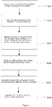
- To be specific, as shown in
Figure 1 , the above preparation method may comprise: - S01, in the case of using a dispersant, pulverizing the raw materials respectively into powder and mixing the same uniformly in proportion, or mixing the raw materials in proportion uniformly and then pulverizing the same, to yield an inorganic mixed powder.
- The dispersant may be chosen from conventional dispersants such as BYK 161 manufactured by BYK Additives & Instruments and Solsperse 32500 and Solsperse 22000 manufactured by The Lubrizol Corporation. Pulverization may be carried out using conventional methods such as ball milling, grinding, and the like. As the inorganic mixed powder may be prepared by existing methods, no further details will be provided herein.
- S02, dissolving from a fourth to a third of an initiator and from a fourth to a third of a diamine in a solvent for later use.
- The mass ratio of the inorganic mixed powder to the substance generated by the reaction of the dianhydride and the diamine is from 20:1 to 1:1.
- That is to say, the amounts of the dianhydride and the diamine are determined as follows: assuming a complete reaction between the dianhydride and the diamine to yield a resultant (which is actually a modified layer), if the mass of the resultant is 1, then the mass of the inorganic mixed powder is between 1 and 20. Such an amount can ensure that a modifier layer with a suitable thickness can be obtained on the inorganic mixed powder.
- An initiator is used to initiate the reaction, which, for example, is a nitrogen-based initiator, preferably any one of azo bisisobutyronitrile, 2,2'-azo bis(2,4-dimethylvaleronitrile), dimethyl azo bisisobutyrate, and azo bisisovaleronitrile.
- The solvent can be selected from fatty alcohols, glycol ethers, ethyl acetate, methyl ethyl ketone, methyl isobutyl ketone, ethylene glycol mono methyl ether, γ-butyrolactone, ethyl 3-ethoxypropionate, butyl carbitol, butyl carbitol acetate, propylene glycol monomethyl ether, propylene glycol monomethyl ether acetate, cyclohexane, xylene, isopropanol, and other conventional organic solvents. Since the choice of the solvent has no significant effect on the performance of the final product, propylene glycol monomethyl ether acetate is used in all the Examples as the solvent.
- S03, adding the inorganic mixed powder to a reaction vessel (e.g., a four-neck flask) which is then subjected to stirring, shocking, shaking and the like; afterwards, adding the dianhydride and the solvent as well as the remaining initiator and diamine and allowing them to be dissolved uniformly.
- S04, heating to carry out the reaction for example in two steps, specifically comprising: heating at a temperature of 35 to 70°C for 20 to 40 min; and then continuing heating at a temperature of 70 to 100°C for 20 to 40 min.
- During the above heating process, the dianhydride and the diamine are allowed to react, thereby generating a modified layer on the surface of the inorganic mixed powder; wherein heating is carried out in two steps so as to prevent the reaction from being too severe.
- During the reaction process, the above solution prepared by dissolving an initiator and a diamine is gradually added dropwise to a four-neck flask so as to prevent the reaction from being too severe.
- The reaction in this step may be carried out, for example, under the protection of nitrogen, and for example under constant stirring.
- The solvent in each step is in an amount sufficient to disperse and dissolve the substances therein uniformly, while the initiator is in an amount sufficient to initiate the reaction, which can be adjusted by those skilled in the art based on the actual conditions, and thus no further detail is given herein. However, the mass ratio (all referring to the total amount) of the inorganic mixed powder, the initiator and the solvent is generally 1 : (from 0.25 to 0.4) : (from 1 to 1.5). To achieve consistency in the process of preparing the functional material in the various Examples, the mass ratio of the inorganic powder, the initiator and the solvent is 1:0.3:1.4.
- S05, cooling the reactant with a refrigerated solvent to room temperature (at about 10 to 30°C) after the reaction is complete.
- S06, evaporating the remaining solvent or separating the powder therefrom, to yield an inorganic mixed powder with a modified layer, i.e., a functional material.
- Of course, it should be appreciated that the preparation method described above may undergo a number of variations, e.g., the dianhydride, the diamine, and the initiator can be dissolved once in the solvent; for another example, heating can be carried out in one step. After all, any variation is allowed as long as the dianhydride and the diamine can react to form a modified layer on the surface of the inorganic mixed powder.
- The infrared emissivity of the functional material is measured according to the
GB/T 7287-2008 - Various functional materials were prepared according to the method described above, where the materials, amounts, parameters and product properties are shown in the following tables.
Table 1. Information about the primary ingredient in the inorganic mixed powder of the functional materials in Examples (content unit: by mass parts) Example # Content of Boron Oxide Content of Sodium Oxide Content of Lithium Oxide Content of Zirconium Oxide 1 3.83 1.83 6.73 20 2 5.18 2.27 8.16 25 3 6.5 3.6 10.5 30 4 7.17 3.6 10.5 30 Table 2. Information about the secondary ingredient in the inorganic mixed powder of the functional materials in Examples (content unit: by mass parts) Example # Secondary Ingredient 1 Type Secondary Ingredient 1 Content Secondary Ingredient 2 Type Secondary Ingredient 2 Content Secondary Ingredient 3 TypeSecondary Ingredient 3 Content1 Silicon Dioxide 40 Manganese Oxide 1.2 Calcium Oxide 0.98 2 Silicon Dioxide 40 Aluminum Nitride 15 Silver Phosphate 3 3 Silicon Dioxide 40 Nickel Oxide 1.4 Chromic Oxide 1.4 4 Alumina 10 Magnesium Oxide 10 None None Table 3. Information about raw materials for preparing a modified layer in the functional materials of Examples Example # Dianhydride Type Diamine Type Mass Ratio of Dianhydride to Diamine Mass Ratio of Inorganic Mixed Powder to Resultant Initiator Type 1 Benzophenone Dianhydride 1,4-bis (aminomethyl) cyclohexane 0.85:1 20:1 Azobisisovaleronitrile 2 Biphenyl Dianhydride 3-amino-benzylamine 0.92:1 1:1 Azobisisovaleronitrile 3 4,4'-(Hexafluoroisopropylide ne)diphthalic anhydride Hexahydro-m-xylylene diamine 1:1 12:1 Azobisisobutyronitrile 4 Pyromellitic Dianhydride 2,7-diamino-fluorene 1.05:1 15:1 2,2'-azobis(2,4-dimethylv aleronitrile) Table 4. Preparation parameters and performance testing results of the functional materials in Examples Example # Heating temperature at the first stage (°C) Heating duration at the first stage (min) Heating temperature at the second stage (°C) Heating duration at the second stage (min) Infrared emissivity (%) Anion concentration (per cubic centimeter) 1 35 40 70 40 85 2572 2 70 20 100 20 88 2466 3 45 35 80 35 92 2785 4 55 25 90 25 94 2810 - As can be seen from the above, all the functional materials of the Examples have a high infrared emissivity and a high anion concentration, which indicates that they actually can produce far-infrared light and anions, thereby improving the environment.
- The present embodiment further provides an organic light emitting diode display panel comprising an organic light emitting diode and an encapsulation structure for encapsulation the organic light emitting diode, wherein the surface and/or interior of the encapsulation structure comprise(s) the above functional material.
- As shown in
Figure 2 , the most primary structure of the organic light emitting diode display panel is a plurality of organic light emitting diodes 1 (which can be provided in an array substrate). However, since the light emitting layer in the organic light emitting diode 1 tends to be affected by water, oxygen and the like, it generally needs to be encapsulated using an encapsulation structure so as to be isolated from the outside environment. - Specifically, the encapsulation structure may comprise an
encapsulation layer 21 and anencapsulation substrate 22;
wherein theencapsulation substrate 22 is typically a glass plate and is assembled with an array substrate in which the organic light emitting diode 1 is located, thereby encapsulating the organic light emitting diode 1 therein. - However, the
encapsulation layer 21 is a layer structure provided on the organic light emitting diode 1 or around the organic light emitting diode 1. According to the difference in the display panel structure, the encapsulation layer may comprise one or more of a sealing layer, an insulating layer (e.g., silicon nitride layer), a getter, a binding layer and the like. As the specific forms of theencapsulation layer 21 are known and diverse, it will not be further described in detail. - For example, the mass percentage of the functional material in the encapsulation structure is 0.1 to 30%; and/or, the surface of the encapsulation structure has a surface film layer with a thickness of 50 to 1000 nm which comprises the functional material in an amount of 0.1 to 10% by mass.
- In other words, the interior of the
encapsulation substrate 22 and/orencapsulation layer 21 may comprise thefunctional material 3 and its mass percentage (based on the total mass 100% of the encapsulation structure and the functional material 3) is, for example, 0.1 to 30%, preferably 3 to 20%. Specifically, thefunctional material 3 can be added to the materials (for example, getters, binders and the like) for forming an encapsulation structure so that thefunctional material 3 is naturally formed therein upon forming an encapsulation structure from the above materials by means of coating and the like. Alternatively, anencapsulating layer 21 such as an insulating layer, a sealing layer and the like is formed by means of chemical vapor deposition (CVD) and the like, and then thefunctional material 3 is incorporated therein by means of sputtering and the like. - Alternatively, a
surface film layer 23 having a thickness of 50 to 1000 nm can be provided on the surface of theencapsulation substrate 22 and/orencapsulation layer 21, and the abovefunctional material 3 is distributed in thesurface film layer 23 in an amount of, for example, 0.1 to 10% by mass, preferably 0.5 to 5% by mass. Specifically, thefunctional material 3 can be dispersed in a solvent to form a suspension which is then applied to the surface of the encapsulation structure by means of coating, spraying and the like. After curing, asurface film layer 23 is formed. - By observing the organic light emitting diode display panel to which the
functional material 3 has been added, it was found out that thefunctional material 3 therein does not involve any phenomenon such as agglomeration, shedding, etc., which suggests that thefunctional material 3 of the present embodiment can be well bonded to the organic light emitting diode display panel and will not produce adverse effects on the properties thereof. - The surface of the inorganic mixed powder in the
functional material 3 of the present embodiment has a modified layer which can allow the inorganic mixed powder to bond well to an encapsulation structure and can improve the ability of the inorganic mixed powder to emit far-infrared rays and negative ions, so that thefunctional material 3 can be well incorporated into the organic light emitting diode display panel to increase its environmental friendliness without affecting the performance of the organic light emitting diode display panel itself. - The organic light emitting diode display panel of the present embodiment is particularly suitable for being used in mobile phones.
- The present application claims the priority of the Chinese Patent Application No.
201410367033.X filed on July 29, 2014
Claims (13)
- A functional material comprising an inorganic mixed powder whose surface has a modified layer, wherein the inorganic mixed powder comprises a primary ingredient and a secondary ingredient;
the primary ingredient consists of boron oxide, sodium oxide, lithium oxide, and zirconium oxide;
the secondary ingredient includes any one or more of aluminum oxide, zinc oxide, titanium dioxide, silicon dioxide, calcium oxide, silver complexes, silver phosphate, silver nitrate, tourmaline, silver thiosulfate, carbon nanotubes, aluminum sulfate, manganese, manganese oxide, iron, iron oxide, cobalt, cobalt oxide, nickel, nickel oxide, chromium, chromium oxide, copper, copper oxide, magnesium oxide, boron carbide, silicon carbide, titanium carbide, zirconium carbide, tantalum carbide, molybdenum carbide, boron nitride, chromium nitride, titanium nitride, zirconium nitride, aluminum nitride, chromium boride, Cr3B4, titanium boride, zirconium boride, tungsten disilicide, and titanium disilicide; characterized in that the modified layer comprises a material obtained from a reaction of a dianhydride and a diamine. - The functional material according to Claim 1, wherein
the dianhydride for generating the modified layer comprises at least one phenyl group; and
the diamine for generating the modified layer comprises at least one phenyl ring or at least one non-phenyl six-membered carbocyclic ring. - The functional material according to Claim 2, wherein
the dianhydride for generating the modified layer is selected from any one of pyromellitic dianhydride, trimellitic anhydride, benzophenone dianhydride, biphenyl dianhydride, diphenyl ether dianhydride, and 4,4'-(hexafluoroisopropylidene)diphthalic anhydride; and
the diamine for generating the modified layer is selected from any one of 3-aminobenzylamine, 2,2'-difluoro-4,4'-(9-fluorenylidene)dianiline, 2,2-bis(3-amino-4-hydroxyphenyl)hexafluoropropane, hexahydro-m-xylylene diamine, 1,4-bis(aminomethyl)cyclohexane, 2,2-bis[4-(4-amino phenoxy)phenyl] hexafluoropropane, 2,2-bis(3-amino-4-methylphenyl)hexafluoropropane, 2,2-bis(3-aminophenyl)hexafluoropropane, 2,2-bis(4-aminophenyl)hexafluoropropane, 2,7-diaminofluorene, m-xylylene diamine, and 4,4'-methylene bis(2-ethyl-6-methylaniline). - The functional material according to any one of Claims 1 to 3, wherein the inorganic mixed powder has a particle diameter of 1 to 5000 nm.
- A method for preparing the functional material according to any one of Claims 1 to 4, the method comprising:mixing the inorganic mixed powder, the dianhydride, and the diamine with an initiator and a solvent uniformly; andreacting the dianhydride with the diamine by heating to form the modified layer on the surface of the inorganic mixed powder.
- The method for preparing the functional material according to Claim 5, wherein the mass ratio of the inorganic mixed powder to the substance generated by the reaction of the dianhydride and the diamine is between 20:1 and 1:1.
- The method for preparing the functional material according to Claim 5, wherein the initiator is any one of azobisisobutyronitrile, 2,2'-azo-bis(2,4-dimethylvaleronitrile), dimethyl azobisisobutyrate and azobisisovaleronitrile.
- The method for preparing the functional material according to Claim 5, wherein the heating comprises two steps:heating at a temperature of 35 to 70°C for 20 to 40 min; andheating at a temperature of 70 to 100°C for 20 to 40 min.
- The method for preparing the functional material according to Claim 5, wherein the molar ratio of the dianhydride to the diamine for generating the modified layer is between 0.85:1 and 1.05:1.
- The method for preparing the functional material according to Claim 9, wherein the molar ratio of the dianhydride to the diamine for generating the modified layer is between 0.92:1 and 1.05:1.
- An organic light emitting diode display panel comprising an organic light emitting diode and an encapsulation structure for encapsulating the organic light emitting diode, wherein the surface and/or interior of the encapsulation structure comprise(s) the functional material according to any one of Claims 1 to 4.
- The organic light emitting diode display panel according to Claim 11, wherein
the interior of the encapsulation structure comprises the functional material in an amount of 0.1 to 30% by mass; and/or
the surface of the encapsulation structure has a surface film layer with a thickness of 50 to 1000 nm which comprises the functional material in an amount of 0.1 to 10% by mass - The organic light emitting diode display panel according to Claim 12, wherein
the interior of the encapsulation structure comprises the functional material in an amount of 3 to 20% by mass; and/or
the surface film layer comprises the functional material in an amount of 0.5 to 5% by mass.
Applications Claiming Priority (2)
| Application Number | Priority Date | Filing Date | Title |
|---|---|---|---|
| CN201410367033.XA CN104277495B (en) | 2013-11-08 | 2014-07-29 | Functional materials and preparation method thereof, organic LED display panel |
| PCT/CN2014/091835 WO2016015408A1 (en) | 2014-07-29 | 2014-11-21 | Functional material, preparation method therefor, organic light-emitting diode display panel |
Publications (3)
| Publication Number | Publication Date |
|---|---|
| EP3176225A1 EP3176225A1 (en) | 2017-06-07 |
| EP3176225A4 EP3176225A4 (en) | 2018-04-11 |
| EP3176225B1 true EP3176225B1 (en) | 2020-02-19 |
Family
ID=55221138
Family Applications (1)
| Application Number | Title | Priority Date | Filing Date |
|---|---|---|---|
| EP14882151.5A Active EP3176225B1 (en) | 2014-07-29 | 2014-11-21 | Functional material, preparation method therefor, organic light-emitting diode display panel |
Country Status (3)
| Country | Link |
|---|---|
| US (1) | US10454062B2 (en) |
| EP (1) | EP3176225B1 (en) |
| WO (1) | WO2016015408A1 (en) |
Families Citing this family (2)
| Publication number | Priority date | Publication date | Assignee | Title |
|---|---|---|---|---|
| US9718724B2 (en) * | 2014-07-29 | 2017-08-01 | Boe Technology Group Co., Ltd. | Functional material, its preparation method, sealing material, and display panel |
| IT201700025506A1 (en) * | 2017-03-08 | 2018-09-08 | Elena Filippi | CABIN FOR BODY TREATMENT WITH IR-EMISSION PANELS AND UV-BEAM EMISSION LAMPS |
Family Cites Families (75)
| Publication number | Priority date | Publication date | Assignee | Title |
|---|---|---|---|---|
| US3863325A (en) | 1973-05-25 | 1975-02-04 | Aluminum Co Of America | Glass cloth in metal forging |
| US4487911A (en) * | 1979-07-23 | 1984-12-11 | The P. D. George Company | Stable polyamic acids |
| JPS61281150A (en) | 1985-06-05 | 1986-12-11 | Nitto Electric Ind Co Ltd | Polyimide powder and production thereof |
| US4996293A (en) | 1987-02-13 | 1991-02-26 | New Japan Chemical Co., Ltd. | Composition comprising polyimide resin from diphenyl sulfone -3,3',4,4'-tetracarboxylic acid dianhydride |
| US4859530A (en) * | 1987-07-09 | 1989-08-22 | Ethyl Corporation | High temperature adhesive for polymide films |
| US4879182A (en) | 1988-10-24 | 1989-11-07 | Ethyl Corporation | Method of coating carbon bodies |
| JPH0551541A (en) * | 1991-08-26 | 1993-03-02 | Mitsubishi Electric Corp | Inorganic filler coated with polyimide resin, resin composition containing the filler, and semiconductor device sealed with the composition |
| US5367012A (en) | 1992-09-10 | 1994-11-22 | Corning Incorporated | Stabilizer for glass/polymer alloys |
| US5344916A (en) | 1993-04-21 | 1994-09-06 | The University Of Akron | Negative birefringent polyimide films |
| AU666441B2 (en) | 1993-05-25 | 1996-02-08 | Lubrizol Corporation, The | Composition utilizing dispersants |
| EP0646632A1 (en) | 1993-09-02 | 1995-04-05 | Loctite (Ireland) Limited | A method of manufacturing a liquid crystal display and a composition for use in the method |
| US5693379A (en) | 1994-10-20 | 1997-12-02 | Chisso Corporation | Polyimide |
| JP3751054B2 (en) * | 1994-11-18 | 2006-03-01 | 宇部興産株式会社 | Adhesive for electronic parts |
| JP2001139345A (en) | 1999-11-10 | 2001-05-22 | Asahi Glass Co Ltd | Leadless low melting point glass and glass frit |
| EP1236756A4 (en) | 2000-08-11 | 2004-06-30 | Mitsui Chemicals Inc | Novel polyimide and circuit substrate comprising the same |
| WO2002061765A1 (en) | 2001-01-29 | 2002-08-08 | Jsr Corporation | Composite particle for dielectrics, ultramicroparticulate composite resin particle, composition for forming dielectrics and use thereof |
| JP2002285031A (en) | 2001-03-27 | 2002-10-03 | Toray Ind Inc | Pigment dispersion liquid, color paste and color filter |
| US6713597B2 (en) | 2002-03-19 | 2004-03-30 | General Electric Company | Preparation of polyimide polymers |
| WO2004023511A1 (en) | 2002-09-03 | 2004-03-18 | Asahi Glass Company, Limited | Pastes for forming barrier ribs and process for production of plasma display panels |
| JP2004149782A (en) | 2002-10-09 | 2004-05-27 | Mitsubishi Chemicals Corp | Thermoplastic resin composition and molded article using the same |
| US7015274B2 (en) | 2003-05-02 | 2006-03-21 | E. I. Du Pont De Nemours And Company | Polymer precursor dispersion containing a micropulp and method of making the dispersion |
| JP2005029584A (en) | 2003-05-15 | 2005-02-03 | Yokohama Rubber Co Ltd:The | Low-molecular weight organic polymer-modified layered clay mineral and rubber composition comprising the same |
| JP2004341381A (en) | 2003-05-19 | 2004-12-02 | Konica Minolta Photo Imaging Inc | Three-dimensional image display method and element |
| JP2004341380A (en) | 2003-05-19 | 2004-12-02 | Konica Minolta Photo Imaging Inc | Three-dimensional image display method and element |
| US7794831B2 (en) | 2003-07-28 | 2010-09-14 | Vampire Optical Coating, Inc. | Anti-reflective coating |
| JP4543695B2 (en) | 2004-02-18 | 2010-09-15 | 住友ベークライト株式会社 | Coated carbon material powder and method for producing the same |
| KR100628698B1 (en) | 2004-02-27 | 2006-09-28 | 대주전자재료 주식회사 | Composition for preparing barrier rib and plasma display panel comprising the barrier rib prepared therefrom |
| JP2006015681A (en) * | 2004-07-05 | 2006-01-19 | Shin Etsu Chem Co Ltd | Metallic foil-polyimide laminated flexible plate and its manufacturing process |
| CN100336847C (en) | 2005-07-14 | 2007-09-12 | 上海交通大学 | In situ synthesis polyimide grafted carbon nano-tube and its preparation method |
| US20070154716A1 (en) | 2005-12-30 | 2007-07-05 | Saint-Gobain Performance Plastics Corporation | Composite material |
| JP5263749B2 (en) | 2006-03-22 | 2013-08-14 | 地方独立行政法人大阪府立産業技術総合研究所 | Polyamide composite particles, polyamic acid composite particles, polyimide composite particles, and production methods thereof |
| JP2009531837A (en) | 2006-03-23 | 2009-09-03 | ソレクサント・コーポレイション | Photovoltaic device containing carbon nanotubes sensitized by nanoparticles |
| US20070231588A1 (en) | 2006-03-31 | 2007-10-04 | Karthikeyan Kanakarajan | Capacitive polyimide laminate |
| TWI317086B (en) | 2006-04-14 | 2009-11-11 | Ritdisplay Corp | Top-emitting organic led display having transparent touch panel |
| KR20080032753A (en) | 2006-10-10 | 2008-04-16 | 삼성전자주식회사 | Ink for forming pattern, method of fabricating the same, light guide plate, light emitting unit and liquid crystal display having the same |
| CN100999589A (en) | 2006-12-22 | 2007-07-18 | 东南大学 | Process for synthesizing composite film of polyacylimide/nano barium phthalate with high deelectric constant |
| CN101260235A (en) | 2007-03-07 | 2008-09-10 | 比亚迪股份有限公司 | Polyimide film and preparation method thereof |
| CN101343425B (en) | 2007-07-10 | 2011-11-16 | 同济大学 | Functionalized carbon nano-tube used as solidifying agent of epoxy resin and preparation method |
| CN101426338A (en) | 2007-10-30 | 2009-05-06 | 达胜科技股份有限公司 | Lamination board and manufacturing method thereof |
| CN101225208B (en) | 2007-12-18 | 2010-06-02 | 福建师范大学 | Method for preparing core-shell structural 'inorganic powder-elastomer' |
| TW201002126A (en) * | 2007-12-21 | 2010-01-01 | Du Pont | Encapsulation assembly for electronic devices |
| JP5233298B2 (en) | 2008-02-01 | 2013-07-10 | 宇部興産株式会社 | Polyimide film and method for producing polyimide film |
| TW201002761A (en) | 2008-07-02 | 2010-01-16 | Taimide Tech Inc | Multi-layered polyimide film and method of manufacturing the same |
| JP5673546B2 (en) * | 2009-09-30 | 2015-02-18 | 大日本印刷株式会社 | Thermally conductive sealing member and electroluminescence element |
| CN102079899B (en) | 2009-11-26 | 2013-05-01 | 京东方科技集团股份有限公司 | Photoconductive ink as well as preparation method and use method thereof |
| CN101805517B (en) * | 2010-03-02 | 2012-05-09 | 天津恒通时代电工材料科技有限公司 | Manufacturing method of inorganic particle filled polyimide film |
| JP2011222333A (en) | 2010-04-09 | 2011-11-04 | Dainippon Printing Co Ltd | Heat conductive sealing member and electronic device sealed thereby |
| ES2548427T3 (en) * | 2010-07-22 | 2015-10-16 | Ferro Corporation | Hermetically sealed electronic device using coated glass flakes |
| CN102039100B (en) | 2010-11-25 | 2013-08-21 | 武汉工程大学 | Amphipathic graft polymer pigment dispersing agent and synthesis process thereof |
| KR20140038538A (en) | 2011-06-28 | 2014-03-28 | 이 아이 듀폰 디 네모아 앤드 캄파니 | Polyimide-coated fillers |
| DE102011078719A1 (en) * | 2011-07-06 | 2013-01-10 | Evonik Degussa Gmbh | Powder containing polymer-coated particles |
| US9193850B2 (en) | 2011-08-11 | 2015-11-24 | Samsung Electronics Co., Ltd. | Nanocomposite, process for preparing the same, and surface emitting device |
| CN102707503A (en) | 2011-08-19 | 2012-10-03 | 北京京东方光电科技有限公司 | Method for dispersing spherical spacers, liquid crystal panel and display device |
| CN102643424B (en) | 2011-08-25 | 2013-10-09 | 北京京东方光电科技有限公司 | Polyimide, as well as preparation method and application thereof |
| CN102707496B (en) | 2011-09-08 | 2014-12-03 | 北京京东方光电科技有限公司 | Liquid crystal orientation film and preparation method thereof, and liquid crystal display device comprising orientation film |
| CN102634020B (en) | 2011-09-19 | 2013-09-11 | 京东方科技集团股份有限公司 | Prepolymer, oriented film, preparation method for oriented film, and liquid crystal display device |
| KR20130035779A (en) * | 2011-09-30 | 2013-04-09 | 코오롱인더스트리 주식회사 | Positive-type photoresist composition, insulating film and oled formed by using the same |
| JP2013140329A (en) | 2011-12-08 | 2013-07-18 | Jnc Corp | Photosensitive composition for transparent conductive film |
| TWI481646B (en) | 2011-12-16 | 2015-04-21 | Taimide Technology Inc | Delustrant composed of polyimide powder, polyimide film incorporating the delustrant, and manufactures thereof |
| TW201414773A (en) | 2012-10-02 | 2014-04-16 | Wintek Corp | Organic light-emitting diode package structure |
| CN102898833B (en) | 2012-10-11 | 2014-09-17 | 京东方科技集团股份有限公司 | Alignment film material, alignment film and preparation method of alignment film, and liquid display device |
| CN103059298B (en) | 2013-01-07 | 2015-02-04 | 北京京东方光电科技有限公司 | Polyamic acid and polyimide, and preparation methods and applications thereof |
| CN103102075B (en) | 2013-01-21 | 2015-05-06 | 京东方科技集团股份有限公司 | Method and device for sealing with frit and frit |
| TWI492970B (en) | 2013-01-28 | 2015-07-21 | Taimide Technology Inc | Colored delustrant powder, polyimide film incorporating the same, and its manufacture methods |
| JP6429465B2 (en) | 2013-03-07 | 2018-11-28 | 株式会社半導体エネルギー研究所 | Apparatus and manufacturing method thereof |
| CN103232609B (en) | 2013-04-25 | 2016-04-20 | 安徽朝日电子新能源有限公司 | A kind of preparation method of flyash modified nano aluminium oxide/polyimide composite film |
| CN103739205B (en) | 2013-11-08 | 2017-06-13 | 北京京东方光电科技有限公司 | Functional material and preparation method thereof, display structure form material, color membrane substrates, display device |
| CN103555003A (en) * | 2013-11-08 | 2014-02-05 | 北京京东方光电科技有限公司 | Modified function material, blue photoresist material and color filter as well as preparation methods thereof and display device |
| WO2016015412A1 (en) * | 2014-07-29 | 2016-02-04 | 京东方科技集团股份有限公司 | Functional material, preparation method therefor, light guide ink, and light guide plate |
| US9587121B2 (en) * | 2014-07-29 | 2017-03-07 | Boe Technology Group Co., Ltd. | Functional material and preparation method thereof, resin composition, film, and display device |
| EP3176224B1 (en) * | 2014-07-29 | 2019-07-10 | Boe Technology Group Co. Ltd. | Three-dimensional display grating, and display device |
| WO2016015407A1 (en) * | 2014-07-29 | 2016-02-04 | 京东方科技集团股份有限公司 | Functional material, preparation method therefor, touch structure, and touch display device |
| US9796928B2 (en) * | 2014-07-29 | 2017-10-24 | Boe Technology Group Co., Ltd. | Functional material, its preparation method, alignment material, and liquid crystal display substrate |
| US10119069B2 (en) * | 2014-07-29 | 2018-11-06 | Boe Technology Group Co., Ltd. | Functional material, its preparation method, color filter material, and color filter substrate |
| CN105077941B (en) * | 2015-07-20 | 2016-08-31 | 京东方科技集团股份有限公司 | A kind of mobile device protection set, mobile device |
-
2014
- 2014-11-21 EP EP14882151.5A patent/EP3176225B1/en active Active
- 2014-11-21 WO PCT/CN2014/091835 patent/WO2016015408A1/en active Application Filing
- 2014-11-21 US US14/769,339 patent/US10454062B2/en active Active
Non-Patent Citations (1)
| Title |
|---|
| None * |
Also Published As
| Publication number | Publication date |
|---|---|
| WO2016015408A1 (en) | 2016-02-04 |
| EP3176225A1 (en) | 2017-06-07 |
| US20160254486A1 (en) | 2016-09-01 |
| US10454062B2 (en) | 2019-10-22 |
| EP3176225A4 (en) | 2018-04-11 |
Similar Documents
| Publication | Publication Date | Title |
|---|---|---|
| CN104277495B (en) | Functional materials and preparation method thereof, organic LED display panel | |
| TWI538943B (en) | Coated magnesium oxide particles, a method for producing the same, a heat-dissipating filler, and a resin composition | |
| TWI308577B (en) | ||
| Lee et al. | Carbon dots for epoxy curing: Anti-forgery patterns with long-term luminescent stability | |
| TW200902646A (en) | Ink-jet ink | |
| EP3176225B1 (en) | Functional material, preparation method therefor, organic light-emitting diode display panel | |
| EP3176224B1 (en) | Three-dimensional display grating, and display device | |
| JP7066962B2 (en) | Antibacterial polymer coating composition and antibacterial polymer film | |
| KR102242545B1 (en) | Antibacterial polymer coating composition and antibacterial polymer film | |
| US9896600B2 (en) | Functional material and method for preparing the same, touch structure and touch display device | |
| US9587121B2 (en) | Functional material and preparation method thereof, resin composition, film, and display device | |
| EP3176226A1 (en) | Functional material, preparation method therefor, alignment material, liquid crystal display substrate | |
| EP3176228B1 (en) | Color film material and color film substrate | |
| EP3176227B1 (en) | Sealing material and display panel | |
| JP2017128662A (en) | Composite filler and thermosetting material | |
| JP2004277657A (en) | Transparent composite sheet | |
| WO2022186034A1 (en) | Resin composition for cutting off blue light using hollow metal oxide particles, and use thereof | |
| Arukula et al. | Aniline‐nonamer segmented polyurea: a facile electrocatalyst for detection of ascorbic acid | |
| KR20210067737A (en) | Antibacterial and anti-allegic polymer coating composition, and antibacterial and anti-allegic polymer film | |
| KR20210080095A (en) | Antibacterial and anti-allegic polymer coating composition, and antibacterial and anti-allegic polymer film | |
| KR20210080094A (en) | Antibacterial and anti-allegic polymer coating composition, and antibacterial and anti-allegic polymer film | |
| JP2023072647A (en) | Dispersion liquid containing metal oxide hollow particles, resin composition and application of the same | |
| KR20210069184A (en) | Antibacterial and anti-allegic polymer coating composition, and antibacterial and anti-allegic polymer film | |
| JP2024019813A (en) | Titanium oxide hollow particles, their manufacturing method, and their uses | |
| JP2019212398A (en) | Uv-curable resin composition for sealing organic el element, method for manufacturing organic el light-emitting device, and organic el light-emitting device |
Legal Events
| Date | Code | Title | Description |
|---|---|---|---|
| 17P | Request for examination filed |
Effective date: 20150820 |
|
| AK | Designated contracting states |
Kind code of ref document: A1 Designated state(s): AL AT BE BG CH CY CZ DE DK EE ES FI FR GB GR HR HU IE IS IT LI LT LU LV MC MK MT NL NO PL PT RO RS SE SI SK SM TR |
|
| AX | Request for extension of the european patent |
Extension state: BA ME |
|
| PUAI | Public reference made under article 153(3) epc to a published international application that has entered the european phase |
Free format text: ORIGINAL CODE: 0009012 |
|
| STAA | Information on the status of an ep patent application or granted ep patent |
Free format text: STATUS: REQUEST FOR EXAMINATION WAS MADE |
|
| DAX | Request for extension of the european patent (deleted) | ||
| A4 | Supplementary search report drawn up and despatched |
Effective date: 20180314 |
|
| RIC1 | Information provided on ipc code assigned before grant |
Ipc: C09C 1/00 20060101ALI20180308BHEP Ipc: H01L 27/32 20060101ALI20180308BHEP Ipc: C09C 3/10 20060101AFI20180308BHEP Ipc: H01L 51/52 20060101ALI20180308BHEP |
|
| STAA | Information on the status of an ep patent application or granted ep patent |
Free format text: STATUS: EXAMINATION IS IN PROGRESS |
|
| 17Q | First examination report despatched |
Effective date: 20190227 |
|
| REG | Reference to a national code |
Ref country code: DE Ref legal event code: R079 Ref document number: 602014061362 Country of ref document: DE Free format text: PREVIOUS MAIN CLASS: C09C0003100000 Ipc: H01L0051520000 |
|
| RIC1 | Information provided on ipc code assigned before grant |
Ipc: C09K 11/67 20060101ALI20190710BHEP Ipc: H01L 27/32 20060101ALI20190710BHEP Ipc: H01L 51/52 20060101AFI20190710BHEP |
|
| GRAP | Despatch of communication of intention to grant a patent |
Free format text: ORIGINAL CODE: EPIDOSNIGR1 |
|
| STAA | Information on the status of an ep patent application or granted ep patent |
Free format text: STATUS: GRANT OF PATENT IS INTENDED |
|
| INTG | Intention to grant announced |
Effective date: 20190827 |
|
| GRAS | Grant fee paid |
Free format text: ORIGINAL CODE: EPIDOSNIGR3 |
|
| GRAA | (expected) grant |
Free format text: ORIGINAL CODE: 0009210 |
|
| STAA | Information on the status of an ep patent application or granted ep patent |
Free format text: STATUS: THE PATENT HAS BEEN GRANTED |
|
| AK | Designated contracting states |
Kind code of ref document: B1 Designated state(s): AL AT BE BG CH CY CZ DE DK EE ES FI FR GB GR HR HU IE IS IT LI LT LU LV MC MK MT NL NO PL PT RO RS SE SI SK SM TR |
|
| REG | Reference to a national code |
Ref country code: CH Ref legal event code: EP |
|
| REG | Reference to a national code |
Ref country code: DE Ref legal event code: R096 Ref document number: 602014061362 Country of ref document: DE |
|
| REG | Reference to a national code |
Ref country code: AT Ref legal event code: REF Ref document number: 1235960 Country of ref document: AT Kind code of ref document: T Effective date: 20200315 |
|
| REG | Reference to a national code |
Ref country code: IE Ref legal event code: FG4D |
|
| REG | Reference to a national code |
Ref country code: NL Ref legal event code: MP Effective date: 20200219 |
|
| PG25 | Lapsed in a contracting state [announced via postgrant information from national office to epo] |
Ref country code: NO Free format text: LAPSE BECAUSE OF FAILURE TO SUBMIT A TRANSLATION OF THE DESCRIPTION OR TO PAY THE FEE WITHIN THE PRESCRIBED TIME-LIMIT Effective date: 20200519 Ref country code: FI Free format text: LAPSE BECAUSE OF FAILURE TO SUBMIT A TRANSLATION OF THE DESCRIPTION OR TO PAY THE FEE WITHIN THE PRESCRIBED TIME-LIMIT Effective date: 20200219 Ref country code: RS Free format text: LAPSE BECAUSE OF FAILURE TO SUBMIT A TRANSLATION OF THE DESCRIPTION OR TO PAY THE FEE WITHIN THE PRESCRIBED TIME-LIMIT Effective date: 20200219 |
|
| REG | Reference to a national code |
Ref country code: LT Ref legal event code: MG4D |
|
| PG25 | Lapsed in a contracting state [announced via postgrant information from national office to epo] |
Ref country code: BG Free format text: LAPSE BECAUSE OF FAILURE TO SUBMIT A TRANSLATION OF THE DESCRIPTION OR TO PAY THE FEE WITHIN THE PRESCRIBED TIME-LIMIT Effective date: 20200519 Ref country code: GR Free format text: LAPSE BECAUSE OF FAILURE TO SUBMIT A TRANSLATION OF THE DESCRIPTION OR TO PAY THE FEE WITHIN THE PRESCRIBED TIME-LIMIT Effective date: 20200520 Ref country code: LV Free format text: LAPSE BECAUSE OF FAILURE TO SUBMIT A TRANSLATION OF THE DESCRIPTION OR TO PAY THE FEE WITHIN THE PRESCRIBED TIME-LIMIT Effective date: 20200219 Ref country code: IS Free format text: LAPSE BECAUSE OF FAILURE TO SUBMIT A TRANSLATION OF THE DESCRIPTION OR TO PAY THE FEE WITHIN THE PRESCRIBED TIME-LIMIT Effective date: 20200619 Ref country code: SE Free format text: LAPSE BECAUSE OF FAILURE TO SUBMIT A TRANSLATION OF THE DESCRIPTION OR TO PAY THE FEE WITHIN THE PRESCRIBED TIME-LIMIT Effective date: 20200219 Ref country code: HR Free format text: LAPSE BECAUSE OF FAILURE TO SUBMIT A TRANSLATION OF THE DESCRIPTION OR TO PAY THE FEE WITHIN THE PRESCRIBED TIME-LIMIT Effective date: 20200219 |
|
| PG25 | Lapsed in a contracting state [announced via postgrant information from national office to epo] |
Ref country code: NL Free format text: LAPSE BECAUSE OF FAILURE TO SUBMIT A TRANSLATION OF THE DESCRIPTION OR TO PAY THE FEE WITHIN THE PRESCRIBED TIME-LIMIT Effective date: 20200219 |
|
| PG25 | Lapsed in a contracting state [announced via postgrant information from national office to epo] |
Ref country code: CZ Free format text: LAPSE BECAUSE OF FAILURE TO SUBMIT A TRANSLATION OF THE DESCRIPTION OR TO PAY THE FEE WITHIN THE PRESCRIBED TIME-LIMIT Effective date: 20200219 Ref country code: PT Free format text: LAPSE BECAUSE OF FAILURE TO SUBMIT A TRANSLATION OF THE DESCRIPTION OR TO PAY THE FEE WITHIN THE PRESCRIBED TIME-LIMIT Effective date: 20200712 Ref country code: SK Free format text: LAPSE BECAUSE OF FAILURE TO SUBMIT A TRANSLATION OF THE DESCRIPTION OR TO PAY THE FEE WITHIN THE PRESCRIBED TIME-LIMIT Effective date: 20200219 Ref country code: DK Free format text: LAPSE BECAUSE OF FAILURE TO SUBMIT A TRANSLATION OF THE DESCRIPTION OR TO PAY THE FEE WITHIN THE PRESCRIBED TIME-LIMIT Effective date: 20200219 Ref country code: EE Free format text: LAPSE BECAUSE OF FAILURE TO SUBMIT A TRANSLATION OF THE DESCRIPTION OR TO PAY THE FEE WITHIN THE PRESCRIBED TIME-LIMIT Effective date: 20200219 Ref country code: LT Free format text: LAPSE BECAUSE OF FAILURE TO SUBMIT A TRANSLATION OF THE DESCRIPTION OR TO PAY THE FEE WITHIN THE PRESCRIBED TIME-LIMIT Effective date: 20200219 Ref country code: SM Free format text: LAPSE BECAUSE OF FAILURE TO SUBMIT A TRANSLATION OF THE DESCRIPTION OR TO PAY THE FEE WITHIN THE PRESCRIBED TIME-LIMIT Effective date: 20200219 Ref country code: RO Free format text: LAPSE BECAUSE OF FAILURE TO SUBMIT A TRANSLATION OF THE DESCRIPTION OR TO PAY THE FEE WITHIN THE PRESCRIBED TIME-LIMIT Effective date: 20200219 Ref country code: ES Free format text: LAPSE BECAUSE OF FAILURE TO SUBMIT A TRANSLATION OF THE DESCRIPTION OR TO PAY THE FEE WITHIN THE PRESCRIBED TIME-LIMIT Effective date: 20200219 |
|
| REG | Reference to a national code |
Ref country code: AT Ref legal event code: MK05 Ref document number: 1235960 Country of ref document: AT Kind code of ref document: T Effective date: 20200219 |
|
| REG | Reference to a national code |
Ref country code: DE Ref legal event code: R097 Ref document number: 602014061362 Country of ref document: DE |
|
| PLBE | No opposition filed within time limit |
Free format text: ORIGINAL CODE: 0009261 |
|
| STAA | Information on the status of an ep patent application or granted ep patent |
Free format text: STATUS: NO OPPOSITION FILED WITHIN TIME LIMIT |
|
| 26N | No opposition filed |
Effective date: 20201120 |
|
| PG25 | Lapsed in a contracting state [announced via postgrant information from national office to epo] |
Ref country code: AT Free format text: LAPSE BECAUSE OF FAILURE TO SUBMIT A TRANSLATION OF THE DESCRIPTION OR TO PAY THE FEE WITHIN THE PRESCRIBED TIME-LIMIT Effective date: 20200219 Ref country code: IT Free format text: LAPSE BECAUSE OF FAILURE TO SUBMIT A TRANSLATION OF THE DESCRIPTION OR TO PAY THE FEE WITHIN THE PRESCRIBED TIME-LIMIT Effective date: 20200219 |
|
| PG25 | Lapsed in a contracting state [announced via postgrant information from national office to epo] |
Ref country code: PL Free format text: LAPSE BECAUSE OF FAILURE TO SUBMIT A TRANSLATION OF THE DESCRIPTION OR TO PAY THE FEE WITHIN THE PRESCRIBED TIME-LIMIT Effective date: 20200219 Ref country code: SI Free format text: LAPSE BECAUSE OF FAILURE TO SUBMIT A TRANSLATION OF THE DESCRIPTION OR TO PAY THE FEE WITHIN THE PRESCRIBED TIME-LIMIT Effective date: 20200219 |
|
| PG25 | Lapsed in a contracting state [announced via postgrant information from national office to epo] |
Ref country code: MC Free format text: LAPSE BECAUSE OF FAILURE TO SUBMIT A TRANSLATION OF THE DESCRIPTION OR TO PAY THE FEE WITHIN THE PRESCRIBED TIME-LIMIT Effective date: 20200219 |
|
| REG | Reference to a national code |
Ref country code: CH Ref legal event code: PL |
|
| GBPC | Gb: european patent ceased through non-payment of renewal fee |
Effective date: 20201121 |
|
| PG25 | Lapsed in a contracting state [announced via postgrant information from national office to epo] |
Ref country code: LU Free format text: LAPSE BECAUSE OF NON-PAYMENT OF DUE FEES Effective date: 20201121 |
|
| REG | Reference to a national code |
Ref country code: BE Ref legal event code: MM Effective date: 20201130 |
|
| PG25 | Lapsed in a contracting state [announced via postgrant information from national office to epo] |
Ref country code: CH Free format text: LAPSE BECAUSE OF NON-PAYMENT OF DUE FEES Effective date: 20201130 Ref country code: LI Free format text: LAPSE BECAUSE OF NON-PAYMENT OF DUE FEES Effective date: 20201130 |
|
| PG25 | Lapsed in a contracting state [announced via postgrant information from national office to epo] |
Ref country code: FR Free format text: LAPSE BECAUSE OF NON-PAYMENT OF DUE FEES Effective date: 20201130 Ref country code: IE Free format text: LAPSE BECAUSE OF NON-PAYMENT OF DUE FEES Effective date: 20201121 |
|
| PG25 | Lapsed in a contracting state [announced via postgrant information from national office to epo] |
Ref country code: GB Free format text: LAPSE BECAUSE OF NON-PAYMENT OF DUE FEES Effective date: 20201121 |
|
| PG25 | Lapsed in a contracting state [announced via postgrant information from national office to epo] |
Ref country code: TR Free format text: LAPSE BECAUSE OF FAILURE TO SUBMIT A TRANSLATION OF THE DESCRIPTION OR TO PAY THE FEE WITHIN THE PRESCRIBED TIME-LIMIT Effective date: 20200219 Ref country code: MT Free format text: LAPSE BECAUSE OF FAILURE TO SUBMIT A TRANSLATION OF THE DESCRIPTION OR TO PAY THE FEE WITHIN THE PRESCRIBED TIME-LIMIT Effective date: 20200219 Ref country code: CY Free format text: LAPSE BECAUSE OF FAILURE TO SUBMIT A TRANSLATION OF THE DESCRIPTION OR TO PAY THE FEE WITHIN THE PRESCRIBED TIME-LIMIT Effective date: 20200219 |
|
| PG25 | Lapsed in a contracting state [announced via postgrant information from national office to epo] |
Ref country code: MK Free format text: LAPSE BECAUSE OF FAILURE TO SUBMIT A TRANSLATION OF THE DESCRIPTION OR TO PAY THE FEE WITHIN THE PRESCRIBED TIME-LIMIT Effective date: 20200219 Ref country code: AL Free format text: LAPSE BECAUSE OF FAILURE TO SUBMIT A TRANSLATION OF THE DESCRIPTION OR TO PAY THE FEE WITHIN THE PRESCRIBED TIME-LIMIT Effective date: 20200219 |
|
| PG25 | Lapsed in a contracting state [announced via postgrant information from national office to epo] |
Ref country code: BE Free format text: LAPSE BECAUSE OF NON-PAYMENT OF DUE FEES Effective date: 20201130 |
|
| REG | Reference to a national code |
Ref country code: DE Ref legal event code: R079 Ref document number: 602014061362 Country of ref document: DE Free format text: PREVIOUS MAIN CLASS: H01L0051520000 Ipc: H10K0050800000 |
|
| PGFP | Annual fee paid to national office [announced via postgrant information from national office to epo] |
Ref country code: DE Payment date: 20231121 Year of fee payment: 10 |