EP3174199A2 - Power management architecture for modulated and constant supply operation - Google Patents
Power management architecture for modulated and constant supply operation Download PDFInfo
- Publication number
- EP3174199A2 EP3174199A2 EP16204437.4A EP16204437A EP3174199A2 EP 3174199 A2 EP3174199 A2 EP 3174199A2 EP 16204437 A EP16204437 A EP 16204437A EP 3174199 A2 EP3174199 A2 EP 3174199A2
- Authority
- EP
- European Patent Office
- Prior art keywords
- power
- radio frequency
- transmit
- signal
- output
- Prior art date
- Legal status (The legal status is an assumption and is not a legal conclusion. Google has not performed a legal analysis and makes no representation as to the accuracy of the status listed.)
- Withdrawn
Links
Images


Classifications
-
- H—ELECTRICITY
- H03—ELECTRONIC CIRCUITRY
- H03F—AMPLIFIERS
- H03F3/00—Amplifiers with only discharge tubes or only semiconductor devices as amplifying elements
- H03F3/20—Power amplifiers, e.g. Class B amplifiers, Class C amplifiers
- H03F3/21—Power amplifiers, e.g. Class B amplifiers, Class C amplifiers with semiconductor devices only
- H03F3/217—Class D power amplifiers; Switching amplifiers
-
- H—ELECTRICITY
- H03—ELECTRONIC CIRCUITRY
- H03F—AMPLIFIERS
- H03F1/00—Details of amplifiers with only discharge tubes, only semiconductor devices or only unspecified devices as amplifying elements
- H03F1/02—Modifications of amplifiers to raise the efficiency, e.g. gliding Class A stages, use of an auxiliary oscillation
- H03F1/0205—Modifications of amplifiers to raise the efficiency, e.g. gliding Class A stages, use of an auxiliary oscillation in transistor amplifiers
- H03F1/0211—Modifications of amplifiers to raise the efficiency, e.g. gliding Class A stages, use of an auxiliary oscillation in transistor amplifiers with control of the supply voltage or current
- H03F1/0216—Continuous control
- H03F1/0222—Continuous control by using a signal derived from the input signal
- H03F1/0227—Continuous control by using a signal derived from the input signal using supply converters
-
- H—ELECTRICITY
- H03—ELECTRONIC CIRCUITRY
- H03F—AMPLIFIERS
- H03F1/00—Details of amplifiers with only discharge tubes, only semiconductor devices or only unspecified devices as amplifying elements
- H03F1/02—Modifications of amplifiers to raise the efficiency, e.g. gliding Class A stages, use of an auxiliary oscillation
- H03F1/0205—Modifications of amplifiers to raise the efficiency, e.g. gliding Class A stages, use of an auxiliary oscillation in transistor amplifiers
- H03F1/0211—Modifications of amplifiers to raise the efficiency, e.g. gliding Class A stages, use of an auxiliary oscillation in transistor amplifiers with control of the supply voltage or current
- H03F1/0216—Continuous control
- H03F1/0233—Continuous control by using a signal derived from the output signal, e.g. bootstrapping the voltage supply
- H03F1/0238—Continuous control by using a signal derived from the output signal, e.g. bootstrapping the voltage supply using supply converters
Definitions
- the embodiments described herein relate to a power management system for delivering current to a linear radio frequency power amplifier. More particularly, the embodiments relate to the use of a pseudo-envelope tracker in a power management system of mobile communications equipment.
- Next-generation mobile devices are morphing from voice-centric telephones to message and multimedia-based "smart" phones that offer attractive new features.
- smart phones offer robust multimedia features such as web-browsing, audio and video playback and streaming, email access and a rich gaming environment. But even as manufacturers race to deliver ever more feature rich mobile devices, the challenge of powering them looms large.
- US2006/0270366 discloses a supply voltage controlled power amplifier that comprises a power amplifier, a closed power control feedback loop configured to generate a power control signal, and a dual voltage regulator coupled to the power control feedback loop, the dual voltage regulator comprising a first regulator stage and a second regulator stage, wherein the closed power control loop minimizes noise generated by the first regulator stage.
- Configuration-feedback circuitry and transceiver circuitry are disclosed, according to a second embodiment of the present disclosure.
- the configuration-feedback circuitry regulates an output power from a radio frequency power amplifier based on a difference between a target output power from the radio frequency power amplifier and a measured output power from the radio frequency power amplifier.
- the transceiver circuitry regulates a modulated power supply voltage, which is used by the radio frequency power amplifier to provide power for amplification, based on the difference between the target output power from the radio frequency power amplifier and the measured output power from the radio frequency power amplifier.
- a power management system which includes a parallel amplifier circuit and a switch mode power supply converter, is disclosed according to a first embodiment of the present disclosure.
- the switch mode power supply converter cooperatively operates with the parallel amplifier circuit to form the power management system.
- the power management system operates in one of a high power modulation mode, a medium power modulation mode, and a low power average power tracking mode. Further, during the high power modulation mode and the medium power modulation mode, the power management system controls a power amplifier supply voltage to a radio frequency power amplifier to provide envelope tracking. During the low power average power tracking mode, the power management system controls the power amplifier supply voltage to the radio frequency power amplifier to provide average power tracking.
- Configuration-feedback circuitry and transceiver circuitry are disclosed, according to a second embodiment of the present disclosure.
- the configuration-feedback circuitry regulates an output power from a radio frequency power amplifier based on a difference between a target output power from the radio frequency power amplifier and a measured output power from the radio frequency power amplifier.
- the transceiver circuitry regulates a modulated power supply voltage, which is used by the radio frequency power amplifier to provide power for amplification, based on the difference between the target output power from the radio frequency power amplifier and the measured output power from the radio frequency power amplifier.
- Figure 1A depicts an embodiment of a pseudo-envelope follower power management system 10A for managing power supplied to a linear radio frequency power amplifier 22 according to one embodiment of the pseudo-envelope follower power management system 10A.
- Figure 1 B depicts an embodiment of a pseudo-envelope follower power management system 10B for managing power supplied to the linear radio frequency power amplifier 22 according to an alternate embodiment of the pseudo-envelope follower power management system 10A.
- Figures 1A and 2A depict an example embodiment of the pseudo-envelope follower power management system 10A including a multi-level charge pump buck converter 12, a parallel amplifier circuit 14, a power inductor 16, a coupling circuit 18, and a bypass capacitor 19.
- the bypass capacitor 19 has a bypass capacitor capacitance, C BYPASS .
- the multi-level charge pump buck converter 12 and the parallel amplifier circuit 14 may be configured to operate in tandem to generate a power amplifier supply voltage, V CC , at a power amplifier supply output 28 of the pseudo-envelope follower power management system 10A for the linear radio frequency power amplifier 22.
- the power amplifier supply voltage, V CC may also be referred to as a modulated power supply voltage, V CC .
- the power amplifier supply output 28 provides an output current, I OUT , to the linear radio frequency power amplifier 22.
- the linear radio frequency power amplifier 22 may include a radio frequency power amplifier input configured to receive a modulated radio frequency input signal having an input power P IN .
- the linear radio frequency power amplifier 22 may further include a radio frequency power amplifier output coupled to an output load, Z LOAD .
- the linear radio frequency power amplifier 22 may generate an amplified modulated radio frequency output signal having an output power P OUT in response to the modulated radio frequency input signal having the input power P IN .
- the output load, Z LOAD may be an antenna.
- the radio frequency power amplifier output may generate the amplified modulated radio frequency output signal as a function of the modulated radio frequency input signal and the power amplifier supply voltage, V CC .
- the power amplifier supply voltage, V CC may be modulated to substantially follow the signal envelope characteristic of the modulated radio frequency input signal to improve the power efficiency of the pseudo-envelope follower power management system 10A.
- the amplified modulated radio frequency output signal may be provided to the antenna for transmission.
- the multi-level charge pump buck converter 12 may include a supply input 24, (V BAT ), configured to receive a battery voltage, V BAT , from a battery 20 and a switching voltage output 26 configured to provide a switching voltage, V SW .
- the switching voltage output 26 may be coupled to the power amplifier supply output 28 by the power inductor 16, where the power inductor 16 couples to the bypass capacitor 19 to form an output filter 29 for the switching voltage output 26 of the multi-level charge pump buck converter 12.
- the power inductor 16 is coupled between the switching voltage output 26 and the power amplifier supply output 28.
- the power inductor 16 provides a power inductor current, I SW_OUT , to the power amplifier supply output 28.
- the parallel amplifier circuit 14 may include a parallel amplifier supply input 30 configured to receive the battery voltage, V BAT , from the battery 20, a parallel amplifier output 32A, a first control input 34 configured to receive a V RAMP signal, and a second control input configured to receive the power amplifier supply voltage, V CC .
- the parallel amplifier output 32A of the parallel amplifier circuit 14 may be coupled to the power amplifier supply voltage V CC , by the coupling circuit 18.
- a parallel amplifier output voltage, V PARA_AMP is provided by the parallel amplifier circuit 14.
- the parallel amplifier circuit 14 may generate the parallel amplifier output voltage, V PARA_AMP , based on the difference between the V RAMP signal and the power amplifier supply voltage, V CC .
- the V RAMP signal may represent either an analog or digital signal that contains the required supply modulation information for a power amplifier collector of a linear radio frequency power amplifier.
- the V RAMP signal is provided to the parallel amplifier circuit 14 as a differential analog signal to provide common mode rejection against any noise or spurs that could appear on this signal.
- the V RAMP signal may be a time domain signal, V RAMP (t), generated by a transceiver or modem and used to transmit radio frequency signals.
- the V RAMP signal may be generated by a digital baseband processing portion of the transceiver or modem, where the digital V RAMP signal, V RAMP_DIGITAL , is digital-to-analog converted to form the V RAMP signal in the analog domain.
- the "analog" V RAMP signal is a differential signal.
- the transceiver or a modem may generate the V RAMP signal based upon a known radio frequency modulation Amp (t)*cos (2*pi*f RF *t + Phase (t)).
- the V RAMP signal may represent the target voltage for the power amplifier supply voltage, V CC , to be generated at the power amplifier supply output 28 of the pseudo-envelope follower power management system 10A, where the pseudo-envelope follower power management system 10A provides the power amplifier supply voltage, V CC , to the linear radio frequency power amplifier 22. Also the V RAMP signal may be generated from a detector coupled to the linear radio frequency power amplifier 22.
- the parallel amplifier circuit 14 includes the parallel amplifier output 32A that provides the parallel amplifier output voltage, V- PARA_AMP , to the coupling circuit 18.
- the parallel amplifier output 32A sources a parallel amplifier circuit output current, I PAWA_OUT , to the coupling circuit 18.
- the parallel amplifier circuit 14, depicted in Figure 1A and Figure 1 B may provide a parallel amplifier circuit output current estimate 40, I PAWA_OUT_EST , to the multi-level charge pump buck converter 12 as an estimate of the parallel amplifier circuit output current I PAWA_OUT , of the parallel amplifier circuit 14.
- the parallel amplifier circuit output current estimate 40 represents an estimate of the parallel amplifier circuit output current I PAWA_OUT , provided by the parallel amplifier circuit 14 as a feedback signal to the multi-level charge pump buck converter 12.
- the multi-level charge pump buck converter 12 may be configured to control the switching voltage, V SW , provided at the switching voltage output 26 of the multi-level charge pump buck converter 12.
- the coupling circuit 18 may be an offset capacitor, C OFFSET .
- An offset voltage, V OFFSET may be developed across the coupling circuit 18.
- the coupling circuit 18 may be a wire trace such that the offset voltage, V OFFSET , between the parallel amplifier output voltage, V PARA_AMP , and the power amplifier supply voltage output, V CC , is zero volts.
- the coupling circuit may be a transformer.
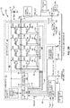
- Figure 2A depicts one embodiment of a pseudo-envelope tracking modulated power supply system 868 according to one embodiment of the pseudo-envelope tracking modulated power supply system 868.
- Figure 2B depicts one embodiment of a pseudo-envelope tracking modulated power supply system 868 according to an alternate embodiment of the pseudo-envelope tracking modulated power supply system 868.
- Figure 2C depicts one embodiment of a pseudo-envelope tracking modulated power supply system 868 according to an additional embodiment of the pseudo-envelope tracking modulated power supply system 868.
- FIG. 2A depicts a high level illustration of a pseudo-envelope tracking modulated power supply system 868 that may include a radio frequency power amplifier 869 configured to be powered by or under the control of a power management system 870.
- the power amplifier supply voltage, V CC may also be referred to as a modulated power supply voltage, V CC , that is generated at a modulated power supply output 876.
- a switch mode power supply converter 872 and a parallel amplifier circuit 874 may be configured to receive an input supply voltage from a battery 20.
- the battery 20 may provide a supply voltage substantially equal to the battery voltage, V BAT .
- the pseudo-envelope tracking modulated power supply system 868 may include a controller 50 coupled via a control bus 44 to the switch mode power supply converter 872 and the parallel amplifier circuit 874.
- the switch mode power supply converter 872 may be arranged to cooperatively operate with the parallel amplifier circuit 874 to form the power management system 870, which generates the modulated power supply voltage, V CC , at the modulated power supply output 876.
- the controller 50 may configure the switch mode power supply converter 872 and the parallel amplifier circuit 874 to operate in various power level modulation modes, depending upon the expected output power to be generated by the radio frequency power amplifier 869 during a transmission of information.
- control functions described with respect to the controller 50 may be incorporated into a digital baseband modem or transceiver circuit that provides a differential V RAMP signal as a control signal to the power management system 870 based on a radio frequency input signal provided to the radio frequency power amplifier 869 for transmission.
- the power management system 870 may be configured to receive a differential V RAMP signal having a non-inverted V RAMP signal component, V RAMP +, and an inverted V RAMP signal component, V RAMP -.
- the power management system 870 may be configured to receive a V RAMP signal that is a single ended V RAMP signal, a differential V RAMP signal, and/or both the single ended V RAMP signal and the differential V RAMP signal.
- the differential V RAMP signal may be provided as a control signal to govern generation of the modulated power supply voltage, V CC .
- the switch mode power supply converter 872 and the parallel amplifier circuit 874 may each be configured to receive the differential V RAMP signal.
- the switch mode power supply converter 872 may include the switching voltage output 26 in communication with the modulated power supply output 876.
- a power inductor 16 may be coupled between the switching voltage output 26 and the modulated power supply output 876.
- the parallel amplifier circuit 874 may include a parallel amplifier circuit output 874A in communication with the modulated power supply output 876.
- a coupling capacitor 18A is coupled between the modulated power supply output 876 and the parallel amplifier circuit output 874A.
- the parallel amplifier circuit 874 may also include a first linear regulator output 874B, LDO 1 OUTPUT, in communication with the modulated power supply output 876.
- the power management system 870 may configure the first linear regulator output 874B, LDO 1 , OUTPUT, to provide a high impedance path with respect to ground.
- the power management system 870 may configure the first linear regulator output 874B, LDO 1 OUTPUT, to apply a first linear regulator output current 878A, I LDO , to the modulated power supply output 876 to regulate the modulated power supply voltage, V CC.
- the parallel amplifier circuit 874 may also include a second linear regulator output 874D, LDO 2 OUTPUT, in communication with a CMOS logic supply input 869C.
- the power management system 870 may configure the second linear regulator output 874D, LDO 2 OUTPUT, to provide a second linear regulator output voltage, V LDO2 , to the CMOS logic supply input 869C as a function of the battery voltage, V BAT .
- the CMOS logic supply input 869C may include a minimum CMOS logic supply voltage threshold.
- the power management system 870 may configure the second linear regulator output 874D, LDO 2 OUTPUT, to provide a second linear regulator output voltage, V LDO2 , to the CMOS logic supply input 869C that is at least equal to the minimum CMOS logic supply voltage threshold.
- the parallel amplifier circuit 874 may also include a switch mode power supply converter control output 874E configured to output a switch mode power supply feedback signal 40A to the switch mode power supply converter 872, depicted in Figures 2B .
- the parallel amplifier circuit 874 may provide a threshold offset current 42, I THRESHOLD_OFFSET , to the switch mode power supply converter 872.
- the parallel amplifier circuit 874 may receive the modulated power supply voltage, V CC , from the modulated power supply output 876 at a modulated power supply voltage feedback input 874F.
- the parallel amplifier circuit 874 may use the input to the modulated power supply voltage feedback input 874F as a feedback signal to regulate the modulated power supply voltage, V CC .
- the radio frequency power amplifier 869 may be a linear radio frequency power amplifier.
- the radio frequency power amplifier 869 may include a radio frequency power amplifier input configured to receive a modulated radio frequency input signal from a digital baseband processing portion of the transceiver or modem, where the modulated radio frequency input signal has an input power, P IN .
- the radio frequency power amplifier 869 may also include a radio frequency power amplifier output in communication with an antenna via the radio frequency duplexer and switch (not shown). The radio frequency power amplifier 869 may generate an amplified modulated radio frequency output signal having an output power P OUT at the radio frequency power amplifier output.
- the radio frequency power amplifier 869 may include a collector voltage supply input 869A configured to receive the modulated power supply voltage, V CC , from the modulated power supply output 876.
- the radio frequency power amplifier 869 may further include a battery voltage supply input 869B configured to receive the battery voltage, V BAT , from the battery 20.
- the radio frequency power amplifier 869 may also include a CMOS logic supply input 869C configured to receive a second linear regulator output voltage, V LDO2 .
- the power management system 870 may be configured to operate in various power level modulation modes based on an expected output power to be generated by the radio frequency power amplifier 869 during a data transmission.
- the power management system 870 may be reconfigured prior to each data transmission to minimize the energy drawn from the battery 20 during the data transmission.
- some embodiments of the power management system 870 may be configured to operate in one of many power level modulation modes on a data transmission slot by data transmission slot basis.
- the power management system 870 may be configured to operate in a set of power level modulation modes including a high power modulation mode, a medium power modulation mode, and low power modulation mode.
- the power management system 870 may be configured to operate in a set of power level modulation modes including a high power modulation mode, a medium power modulation mode, a medium power average power tracking modulation modes, and a low power average power tracking modulation mode.
- the medium power average power tracking modulation modes are omitted.
- the power management system 870 may disable the switch mode power supply converter 872, and configure the parallel amplifier circuit 874 to track an envelope of a modulated radio frequency input signal to be transmitted by the radio frequency power amplifier 869 as a function of a slowly modulated or unmodulated differential V RAMP signal.
- the power management system 870 may further configure the parallel amplifier circuit 874 to provide a modulated power supply voltage, V CC , based on a substantially unmodulated differential V RAMP signal.
- the power management system 870 may be configured to generate a modulated power supply voltage, V CC that has a substantially fixed voltage level.
- the parallel amplifier circuit 874 may be configured to slowly track the envelope of the differential V RAMP signal.
- the power management system 870 may enable and disable various elements and signal processing functions of the switch mode power supply converter 872 and the parallel amplifier circuit 874 as a function of the power level modulation mode of operation.
- the power management system 870 may disable the least energy efficient element and signal processing functions as a function of the expected output power to be generated by the radio frequency power amplifier 869.
- the power management system 870 may disable portions of the switch mode power supply converter 872, the parallel amplifier circuit 874, and/or a combination thereof as the expected output power of the radio frequency power amplifier 869 decreases to achieve an overall decrease in energy consumption from the battery 20 during a data transmission.
- some embodiments of the power management system 870 may generate the modulated power supply output 876 using a less energy efficient device or power generation circuit in response to an expected output power of the radio frequency power amplifier 869 falling below a low power modulation mode threshold in order to disable other energy consuming circuitry and achieve an overall reduction in energy drawn from the battery 20 during a data transmission.
- the power management system 870 may configure the switch mode power supply converter 872 and the parallel amplifier circuit 874 to generate the modulated power supply voltage, V CC , based on the differential V RAMP signal as a function of the expected output power to be generated by the radio frequency power amplifier 869 during the data transmission.
- the parallel amplifier circuit 874 may be configured to govern the operation of the switch mode power supply converter 872, regulate generation of the modulated power supply voltage, V CC , as a function of the differential V RAMP signal, and regulate the offset voltage, V OFFSET , across the coupling capacitor 18A.
- the switch mode power supply converter 872 boosts the power amplifier supply voltage, V CC , above the battery voltage, V BAT .
- the power amplifier supply voltage, V CC is modulated and provides envelope tracking. Further, during the low power average power tracking mode, the power amplifier supply voltage, V CC , is not modulated and provides average power tracking. In this regard, during the low power average power tracking mode, a magnitude of the power amplifier supply voltage, V CC , is adjustable based on an expected output power from the radio frequency power amplifier 869.
- the parallel amplifier circuit 874 may be configured to apply a parallel amplifier circuit output current, I PAWA_OUT , from the parallel amplifier circuit 874 to regulate the modulated power supply voltage, V CC , as a function of the differential V RAMP signal.
- the parallel amplifier circuit 874 may provide the switch mode power supply feedback signal 40A and a threshold offset current 42, I THRESHOLD_OFFSET , to govern the operation of the switch mode power supply converter 872 and regulate the offset voltage, OFFSET, across the coupling capacitor 18A.
- the switch mode power supply converter 872 may generate the switching voltage, V SW , at the switching voltage output 26, and provide a delayed I COR estimated switching voltage output 38C, V SW_EST_DELAY_ICOR , to the parallel amplifier circuit 874.
- the parallel amplifier circuit 874 may configure the first linear regulator output 874B, LDO 1 OUTPUT, to provide a high impedance path to ground.
- the parallel amplifier circuit 874 may configure the second linear regulator output 874D, LDO 2 OUTPUT, to provide the second linear regulator output voltage, V LDO2 , at least equal to the minimum CMOS logic supply voltage to the CMOS logic supply input 869C of the radio frequency power amplifier 869.
- the power management system 870 may disable the switch mode power supply converter 872 and configure the switching voltage output 26 to provide a high impedance path to ground.
- the parallel amplifier circuit output 874A may be configured to provide a low impedance path to ground to short the negative terminal of the coupling capacitor 18A to ground.
- the first linear regulator output 874B, LDO 1 , OUTPUT may be configured to apply a linear regulator output current, I LDO , to the modulated power supply output 876 as a function of the differential V RAMP signal and a selected tracking mode of operation.
- the differential V RAMP signal may be substantially constant or only slowly modulated during the data transmission.
- the power management system 870 may configure the parallel amplifier circuit 874 to operate in a no tracking mode of operation. In the no tracking mode of operation, the first linear regulator output 874B, LDO 1 , OUTPUT, may regulate the modulated power supply voltage, V CC , to be substantially constant or unmodulated during data transmission.
- the power management system 870 may configure the first linear regulator output 874B, LDO 1 OUTPUT, to slowly track the differential V RAMP signal during the data transmission.
- the parallel amplifier circuit 874 may disable the second linear regulator output 874D, LDO 2 OUTPUT. In some alternative embodiments of the low power modulation mode, the parallel amplifier circuit 874 may configure the second linear regulator output 874D, LDO 2 OUTPUT, to selectively output the second linear regulator output voltage, V LDO2 , to the CMOS logic supply input 869C as a function of the battery voltage, V BAT .
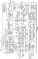
- Figure 2B depicts a non-limiting example of the embodiments of the switch mode power supply converter 872 that may be selectively configured to operate in a number of various buck converter modes, a number of various envelope tracking modes, a number of various average power tracking modes, and/or a combination thereof as a function of an expected output power to be generated by the radio frequency power amplifier 869 depicted in Figures 2A and 2C .
- the switch mode power supply converter 872 may further include an off mode.
- the various embodiments of the switch mode power supply converter 872 are described with continuing reference to the various embodiments of the power management system 870, depicted in Figures 2A-C .
- the various envelope tracking modes may include one or more envelope tracking power modes of operation including the high power modulation mode and the medium power modulation mode.
- the various average power tracking modes may include one or more average power tracking modes of operation including a medium power average power tracking mode and a low power average power tracking mode.
- the switch mode power supply converter 872 is arranged to cooperatively operate with the parallel amplifier circuit 874 to form the power management system 870, which operates in one of the high power modulation mode, the medium power modulation mode, and the low power average power tracking mode.
- the power management system 870 operates in one of the high power modulation mode, the medium power modulation mode, the medium power average power tracking mode, and the low power average power tracking mode.
- the power management system 870 provides envelope tracking using the power amplifier supply voltage, V CC , during the high power modulation mode and the medium power modulation mode.
- the power management system 870 controls the power amplifier supply voltage, V CC , to the linear radio frequency power amplifier 22 to provide the envelope tracking.
- the pseudo-envelope tracking modulated power supply system 868 provides average power tracking during the low power average power tracking mode.
- the power management system 870 controls the power amplifier supply voltage, V CC , to the linear radio frequency power amplifier 22 to provide the average power tracking.
- the linear radio frequency power amplifier 22 sequentially transmits multiple communications slots.
- selection of the one of the high power modulation mode, the medium power modulation mode, and the low power average power tracking mode is based on an expected output power from the radio frequency power amplifier 869 and is made on a communications slot to communications slot basis.
- adjustment of a magnitude of the power amplifier supply voltage, V CC is made on a communications slot to communications slot basis.
- the controller 50 may configure the switch mode power supply converter 872 to operate in the medium power average power tracking mode when the power management system 870 is configured to operate in a medium power average power tracking modulation mode.
- the controller 50 may configure the switch mode power supply converter 872 to be in a high power modulation mode when the power management system 870 is configured to operate in the high power modulation mode.
- the controller 50 may configure the switch mode power supply converter 872 to be in a medium power modulation mode when the power management system 870 is configured to operate in the medium power modulation mode.
- the controller 50 may configure the switch mode power supply converter 872 to be in an off mode when the power management system 870 is configured to operate in either a low power modulation mode or a low power average power tracking mode.
- the switch mode power supply converter 872 may include embodiments of a switcher control circuit 880, a multi-level charge pump 882, a switching circuit 884, and an average frequency control circuit 885.
- the switcher control circuit 880, the multi-level charge pump 882, the switching circuit 884, and a feedback delay compensation circuit 852 may be configured to receive the battery voltage, V BAT .
- Some embodiments of the switch mode power supply converter 872 may further include the feedback delay compensation circuit 852.
- the controller 50 may configure the switcher control circuit 880 to govern the operation of the multi-level charge pump 882 and the switching circuit 884 as a function of the power level modulation mode and the expected output power to be generated by the embodiments of the radio frequency power amplifier 869 in response to a modulated radio frequency input signal to be transmitted.
- the switcher control circuit 880 may also be configured to control the operation of the feedback delay compensation circuit 852 as a function of the power level modulation mode and the expected output power of the radio frequency power amplifier 869.
- the feedback delay compensation circuit 852 may generate a feedback delay compensation signal 854, I FEEDBACK_TC , as a function of the power level modulation mode and the expected output power of the radio frequency power amplifier 869.
- the controller 50 or the switcher control circuit 880 may configure the feedback delay compensation circuit 852 to operate as a function of a high power mode apparent gain to increase the aggressiveness of the feedback compensation provided by the feedback delay compensation signal 854, I FEEDBACK_TC .
- the switch mode power supply converter 872 may respond to a change in the target voltage for the modulated power supply voltage, V CC , provided by the differential V RAMP signal, which may increase the power efficiency of the various embodiments of a parallel amplifier 928, depicted in Figure 2C .
- the controller 50 or the switcher control circuit 880 may configure the feedback delay compensation circuit 852 to operate as a function of a medium power mode apparent gain to decrease the aggressiveness of the feedback compensation provided by the feedback delay compensation signal 854, I FEEDBACK_TC , in order to prevent the switcher control circuit 880 from pre-maturely changing the switching voltage, V SW .
- the feedback delay compensation circuit 852 may operate in an overly aggressive manner when the apparent gain is set too high with respect to the expected output power to be generated by the radio frequency power amplifier 869 during a data transmission.
- the switch mode power supply converter 872 may overreact to a change in the target voltage for the modulated power supply voltage, V CC , provided by the differential V RAMP signal.
- the switch mode power supply converter 872 may generate a switching voltage that provides too much or too little energy to the modulated power supply voltage V CC , which may decrease the power efficiency of the various embodiments of the parallel amplifier 928, depicted in Figure 2C .
- the controller 50 may set the apparent gain of the feedback delay compensation circuit 852 based on a sliding scale as a function of the expected output power to be generated by the radio frequency power amplifier 869 during the data transmission.
- some embodiments of the switcher control circuit 880 may be further configured to adjust the apparent gain of the feedback delay compensation circuit 852 based on a segmentation mode of the switching circuit 884.
- the controller 50 or the switcher control circuit 880 may disable the feedback delay compensation circuit 852 during the low power average power tracking mode and during the off mode.
- Some embodiments of the power management system 870 may enable the feedback delay compensation circuit 852 in a high power modulation mode and a medium power modulation mode.
- the switcher control circuit 880 may disable the multi-level charge pump 882 and the switching circuit 884, and configure the switching voltage output 26 to provide a high impedance path to ground.
- the switch mode power supply converter 872 may be configured to disable a clocking signal that may be used by a ⁇ C charge pump circuit 262.
- the switcher control circuit 880 may disable the multi-level charge pump 882, and control the switching circuit 884 to swing the switching voltage, V SW , between the battery voltage, V BAT , and ground.
- the switcher control circuit 880 may enable both the multi-level charge pump 882 and the switching circuit 884.
- the switcher control circuit 880 may further control the multi-level charge pump 882 and the switching circuit 884 to generate both buck level voltages and boost level voltages to provide the switching voltage, V SW , at the switching voltage output 26 as a function of the operational state of the switcher control circuit 880 and the power level modulation mode.
- the switcher control circuit 880 may be configured to operate in a number of average power tracking "bang-bang" modes of operation.
- the switcher control circuit 880 may configure the multi-level charge pump 882 and the switching circuit 884 to switch the switching voltage, V SW , between only a first bang-bang switching voltage, V SW_BB1 , and a second bang-bang switching voltage, V SW_BB2 , during a data transmission, where the first bang-bang switching voltage, V SW _ BB1 , is less than the second bang-bang switching voltage, V SW_BB2 .
- the first bang-bang switching voltage, V SW_BB1 may be substantially equal to ground, the battery voltage, V BAT , or the switching voltage V SW between ground and the battery voltage, V BAT .
- the second bang-bang switching voltage, V SW _ BB2 may be substantially equal to the supply voltage, V BAT , or a charge pump output voltage generated by the multi-level charge pump 882 from the battery voltage, V BAT .
- the average power tracking "bang-bang" modes of operation may include an average power tracking "buck-buck" mode of operation and an average power tracking "buck-boost" mode of operation.
- the switcher control circuit 880 may configure the multi-level charge pump 882 and the switching circuit 884 to generate a first bang-bang switching voltage, V SW_BB1 , and a second bang-bang switching voltage, V SW_BB2 , that are no greater than the battery voltage, V BAT .
- the switcher control circuit 880 may configure the multi-level charge pump 882 to generate only a bucked output voltage at a charge pump output 64.
- the switcher control circuit may configure the multi-level charge pump 882 to generate a first buck mode output voltage, V FIRST_BUCK , substantially equal to 1/2 x V BAT in a first buck mode of operation.
- the switcher control circuit 880 may disable the multi-level charge pump 882 provided the first bang-bang switching voltage, V SW _ BB1 , and the second bang-bang switching voltage, V SW_BB2 , are a shunt mode output voltage substantially equal to ground and a series mode output voltage substantially equal to V BAT , respectively.
- the first bang-bang switching voltage, V SW_BB1 may be no greater than the battery voltage, V BAT
- the second bang-bang switching voltage, V SW_BB2 is a boost voltage that is greater than the battery voltage, V BAT
- the switcher control circuit 880 may configure the multi-level charge pump 882 and the switching circuit 884 to generate the first bang-bang switching voltage, V SW_BB1 .
- the switcher control circuit 880 may configure the multi-level charge pump 882 to generate the second bang-bang switching voltage, V SW_BB2 .
- Some embodiments of the switcher control circuit 880 may be configured to form a composite control signal as a function of the various envelope tracking modes, the various average power tracking modes, and buck converter modes.
- the various embodiments of the switcher control circuit 880 may combine the various fractional amounts and combinations of the feedback delay compensation signal 854, I FEEDBACK_TC , the switch mode power supply feedback signal 40A, and the threshold offset current 42, I THRESHOLD_OFFSET , to form one or more composite control signals as a function of the power level modulation mode.
- the composite control signal may depend on the power level modulation mode.
- Figure 2C depicts an embodiment of the power management system 870 in which a parallel amplifier 928 may generate the switch mode power supply feedback signal 40A in the high power modulation mode and medium power modulation mode.
- a V OFFSET loop circuit 41 may generate the threshold offset current 42, I THRESHOLD_OFFSET , in the high power modulation mode and the medium power modulation mode.
- the switcher control circuit 880 may also provide a series switch control signal 66 and a shunt switch control signal 68 to the switching circuit 884.
- the switching circuit 884 couples the switching voltage output 26 to the battery voltage, V BAT , to generate the switching voltage, V SW , substantially equal to V BAT .
- the switching circuit 884 couples the switching voltage output 26 to ground to generate the switching voltage, V SW , substantially equal to zero.
- the switcher control circuit 880 provides a segmentation control signal 880A to the switching circuit 884 as a function of the power level modulation mode.
- the switcher control circuit 880 may generate the segmentation control signal 880A as a function of the power level modulation mode and the expected output power to be generated by the radio frequency power amplifier 869 during a data transmission.
- some embodiments of the power management system 870 may be configured to generate the segmentation control signal 880A based on an average expected output power, P OUT_AVE , of the radio frequency power amplifier 869 that maximizes the efficiency of the switch mode power supply converter 872.
- the switch mode power supply converter 872 has a segmented output stage, such that during the high power modulation mode and the medium power modulation mode, segment selection of the segmented output stage is based on an expected output power from the radio frequency power amplifier 869 to increase efficiency of the pseudo-envelope tracking modulated power supply system 868.
- the switcher control circuit 880 may configure the switch mode power supply converter 872 to generate a switching voltage, V SW , at the switching voltage output 26 based on an operational state of the switcher control circuit 880 as a function of a power level modulation mode, which is dependent on the expected output power to be generated by the radio frequency power amplifier 869 during a data transmission.
- the switcher control circuit 880 may configure the multi-level charge pump 882 and the switching circuit 884 to operate in one of a buck converter "bang-bang" mode, a multi-level charge pump buck converter mode, and an average power tracking mode of operation as a function of the power level modulation mode and operational mode of the switcher control circuit 880.
- a control signal 926 received at the non-inverting input of the parallel amplifier 928 to generate the parallel amplifier output current, I PARA_AMP , may be generated by a differential filter 924 as a function of the power level modulation mode.
- the differential filter 924 may provide an increased level of frequency compensation or correction as compared to the frequency compensation or correction provided by the differential filter 924 in the medium power modulation mode.
- some embodiments of the switcher control circuit 880, the switch mode power supply converter 872, the parallel amplifier circuit 874 and/or a combination thereof may be further adapted to adjust a scaling factor, M, provided to a buffer scalar 434, and/or the magnitude of the delayed I COR estimated switching voltage output 38C, V SW_EST_DELAY_ICOR , as a function of the power level modulation mode.
- Some alternative embodiments of the switcher control circuit 880, the switch mode power supply converter 872, the parallel amplifier circuit 874, and/or combinations thereof, may be further configured to adjust the magnitude of the delayed I COR estimated switching voltage output 38C, V SW_EST_DELAY_ICOR , based on the magnitude of the control signal 926 that is received by at the non-inverting input of the parallel amplifier 928, which is generated by the differential filter 924.
- the switcher control circuit 880 may selectively adjust the scaling factor, M, as a function of the magnitude of the differential V RAMP signal and the power level modulation mode.
- the scaling factor, M may be further adjusted as a function of the power level modulation mode to reflect the amount of frequency compensation or correction applied by the differential filter 924 to generate the control signal 926 received at the non-inverting input 928A of the parallel amplifier 928, depicted in Figure 2C .
- either the switch mode power supply converter 872 or the parallel amplifier circuit 874 may be further adapted to adjust the scaling factor, M, based on the magnitude of the control signal 926 or the power level modulation mode.
- the magnitude of the delayed I COR estimated switching voltage output 38C, V SW_EST_DELAY_ICOR may be adjusted as a function of the power level modulation mode, the magnitude of the differential V RAMP signal, and the expected frequency response of the parallel amplifier 928 when operating in each of the respective power level modulation modes.
- a switcher propagation delay is a time period between when the state of the switcher control circuit 880 changes to a new operational state and the switching voltage, V SW , generated in response to the new operational state of the switcher control circuit 880, is generated at the switching voltage output 26.
- the switcher propagation delay may vary based on being configured to operate in the envelope tracking mode of operation and the average power tracking mode.
- the controller 50 may be configured to adjust the programmable delay period as a function of an expected output power to be generated by the radio frequency power.
- the switching circuit 884 may be a segmented switching circuit having a number of sets of series switch and shunt switch pairs.
- the sets of series switch and shunt switch pairs may be arranged in parallel and operably coupled to form a segmented series switch and shunt switch network.
- the switcher control circuit 880 may generate a series switch control signal 66, a shunt switch control signal 68, and the segmentation control signal 880A based on an operational state of the switcher control circuit 880 to control the operation of the switching circuit 884.
- the segmentation control signal 880A may be dependent on the power level modulation mode of the power management system 870.
- the switcher control circuit 880 may configure the segmentation control signal 880A to enable or disable various combinations of the sets of series switch and shunt switch pairs of the switching circuit 884 based on the power level modulation mode of operation of the respective power management system 870, depicted in Figure 2A-C .
- the switcher control circuit 880 may generate a segmentation control signal 880A to enable either 75% or 50% of the number of sets of series switch and shunt switch pairs of the switching circuit 884.
- the switcher propagation delay may vary depending on the number of sets of series switch and shunt switch pairs configured to operate during a data transmission.
- the switcher control circuit 880 may be configured to adjust a programmable delay period depending on the segmentation control signal 880A to maintain the temporal alignment of the delayed I COR estimated switching voltage output 38C V SW_EST_DELAY_ICOR with respect to the switching voltage, V SW , provided at the switching voltage output 26.
- the switching circuit 884 may include a segmentation control circuit 886 configured to receive a segmentation control signal 880A from the switcher control circuit 880.
- the switching circuit 884 may further include segmented series switches 888 and segmented shunt switches 890 in communication with the segmentation control circuit 886.
- the segmented series switches 888 may include a first series switch 892, a second series switch 894, a third series switch 896, and a fourth series switch 898.
- the segmented shunt switches 890 may include a first shunt switch 900, a second shunt switch 902, a third shunt switch 904, and a fourth shunt switch 906.
- a source 892S of the first series switch 892, a source 894S of the second series switch 894, a source 896S of the third series switch 896, and a source 898S of the fourth series switch 898 are in communication with a supply voltage received from the battery 20 substantially equal to the battery voltage, V BAT .
- a drain 892D of the first series switch 892, a drain 894D of the second series switch 894, a drain 896D of the third series switch 896, and a drain 898D of the fourth series switch 898 are respectively coupled to a drain 900D of the first shunt switch 900, a drain 902D of the second shunt switch 902, a drain 904D of the third shunt switch 904, and a drain 906D of the fourth shunt switch 906 to form the switching voltage output 26.
- a source 900S of the first shunt switch 900, a source 902S of the second shunt switch 902, a source 904S of the third shunt switch 904, and a source 906S of the fourth shunt switch 906 are in communication with a reference voltage substantially equal to ground.
- the segmentation control circuit 886 may include a first series switch control output 908 coupled to the gate 892G of the first series switch 892, a first shunt switch control output 910 coupled to the gate 900G of the first shunt switch 900, a second series switch control output 912 coupled to the gate 894G of the second series switch 894, a second shunt switch control output 914 coupled to the gate 902G of the second shunt switch 902, a third series switch control output 916 coupled to the gate 896G of the third series switch 896, a third shunt control output 918 coupled to the gate 904G of the third shunt switch 904, a fourth series switch control output 920 couple to the gate 898G of the fourth series switch 898, and a fourth shunt switch control output 922 coupled to the gate 906G of the fourth shunt switch 906.
- the segmentation control circuit 886 may divide the segmented series switches 888 and segmented shunt switches 890 into logical groupings of sets of series and shunt switches such that each set of series and shunt switches includes one of the segmented series switches 888 and one of the segmented shunt switches 890.
- a first set of series and shunt switches may include the first series switch 892 and the first shunt switch 900.
- a second set of series and shunt switches may include the second series switch 894 and the second shunt switch 902.
- a third set of series and shunt switches may include the third series switch 896 and the third shunt switch 904.
- a fourth set of series and shunt switches may include the fourth series switch 898 and the fourth shunt switch 906.
- the segmentation control circuit 886 is configured to receive a series switch control signal 66 and a shunt switch control signal 68 from the switcher control circuit 880.
- the power management system 870 may configure the switcher control circuit 880 to generate a segmentation control signal 880A to select which of the segmented series switches 888 and segmented shunt switches 890 are to be enabled by the segmentation control circuit 886 to generate the switching voltage, V SW , at the switching voltage output 26 as a function of the average expected output power, P OUT_AVE , to be generated by the radio frequency power amplifier 869 during the data transmission.
- the operation of the segmentation control circuit 886 may be divided into four regions or modes of operation.
- the switcher control circuit 880 may generate the segmentation control signal 880A as a function of the average expected output power, P OUT_AVE , and a set of switcher output power thresholds including a first switcher output power threshold, P OUT1 , a second switcher output power threshold, P OUT2 , and a third switcher output power threshold, P OUT3 .
- the values of the first switcher output power threshold, P OUT1 , the second switcher output power threshold, P OUT2 , and the third switcher output power threshold, P OUT3 may be determined to maximize the efficiency of the switch mode power supply converter 872 with respect to the expected output power of the radio frequency power amplifier 869 as a function of the power level modulation mode and an expected load line, R RF_AMP_EXP , of the radio frequency power amplifier 869 during the data transmission.
- the segmentation control signal 880A may configure the segmentation control circuit 886 to enable all four of the series switch and shunt switch segments.
- the segmentation control signal 880A may configure the segmentation control circuit 886 to enable three of the series switch and shunt switch segments.
- the segmentation control signal 880A may configure the segmentation control circuit 886 to enable two of the series switch and shunt switch segments. And in the case where the average expected output power, P OUT_AVE , of the radio frequency power amplifier 869 is less than the third switcher output power threshold, P OUT3 , the segmentation control signal 880A may configure the segmentation control circuit 886 to enable one of the series switch and shunt switch segments.
- the multi-level charge pump 882 may configure a multi-level charge pump switching network to generate a variety of "boost" output voltages and "buck" output voltages as a function of a charge pump mode control signal 62 received from the switcher control circuit 880. Some embodiments of the multi-level charge pump 882 may generate a variety of "boost” output voltages and “buck” output voltages as a multi-level charge pump output voltage, V MLCP , in response to the charge pump mode control input 62 generated by the switcher control circuit 880. The multi-level charge pump 882 may provide the multi-level charge pump output voltage, V MLCP , to the charge pump output 64, which may be coupled through the switching circuit 884 to the switching voltage output 26.
- the multi-level charge pump 882 may configure the multi-level charge pump switching network to generate a second boost mode output voltage, V SECOND_BOOST , substantially equal to 2 x V BAT at the charge pump output 64.
- V SECOND_BOOST second boost mode output voltage
- the multi-level charge pump 882 may configure the switching network to generate a first boost mode output voltage at the charge pump output 64 substantially equal to 3/2 x V BAT .
- the multi-level charge pump 882 may configure the multi-level charge pump switching network to generate a first buck mode output voltage at the charge pump output 64 substantially equal to 1/2 x V BAT .
- the multi-level charge pump 882 may be configured to generate other ratios of boost mode output voltages and buck mode output voltage.
- Some embodiments of the multi-level charge pump 882 may include only two flying capacitors that are coupled in various switching arrangements with respect to each other, the battery voltage, V BAT , and the charge pump output 64 to generate the various charge pump output voltages at the charge pump output 64.
- some embodiments of the multi-level charge pump 882 may generate various ratios of output voltages that may be provided as a boost output voltage or a buck output voltage to the switching voltage output 26 as the switching voltage, V SW .
- the multi-level charge pump 882 may generate a boost output voltage or a buck output voltage with respect to a supply voltage other than the battery voltage, V BAT , where the supply voltage may be greater than the battery voltage, V BAT , or less than the battery voltage, V BAT .
- the supply voltage provided to the multi-level charge pump 882 may be a boosted voltage or a bucked voltage derived from the battery voltage, V BAT .
- the switcher control circuit 880 may configure the switch mode power supply converter 872 to generate a series output voltage substantially equal to the battery voltage, V BAT , a shunt output voltage substantially equal to a ground voltage, and a subset of the available charge pump output voltages.
- the switcher control circuit 880 may configure the multi-level charge pump 882 and the switching circuit 884 to generate a shunt mode output voltage substantially equal to a ground voltage in the shunt output mode, a series mode output voltage substantially equal to V BAT in the series output mode, and a first boost mode output voltage V FIRST_BOOST substantially equal to 3/2 x V BAT in the first boost output mode.
- the switcher control circuit 880 may configure the multi-level charge pump 882 to provide a first buck mode output voltage substantially equal to 1/2 x V BAT in the first buck mode of operation.
- the switcher control circuit 880 may configure the multi-level charge pump 882 and the switching circuit 884 to generate a shunt mode output voltage substantially equal to ground, a first buck mode output voltage substantially equal to 1/2 x V BAT , a series mode output voltage substantially equal to V BAT , and a first boost mode output voltage substantially equal to 3/2 x V BAT as a function of the operational state of the switcher control circuit 880.
- the switcher control circuit 880 may configure the multi-level charge pump 882 to only operate in a first boost mode of operation to generate a first boost mode output voltage, V FIRST_BOOST , substantially equal to 3/2 x V BAT .
- the multi-level charge pump 882 may be configured to only operate in the second boost mode of operation. In still another example, in some power level modulation modes, the multi-level charge pump 882 may be configured to operate in the first buck mode and either the first boost mode or the second boost mode of operation.
- the switcher control circuit 880 may configure the multi-level charge pump 882 to provide either a first buck mode output voltage substantially equal to 1/2 x V BAT and a first boost mode output voltage substantially equal to 3/2 x V BAT as a function of the operational state of the switcher control circuit 880.
- the switcher control circuit may configure the multi-level charge pump 882 to provide a buck output voltage substantially equal to 1/2 x V BAT in the first buck mode and a second boost level output voltage substantially equal to 2 x V BAT as a function of the operational state of the switcher control circuit 880.
- the controller 50 may configure the comparator thresholds to set the equivalent main ripple voltage level at the modulated power supply output 876 and/or the switching frequency of the switch mode power supply converter 872. For example, in the medium power average power tracking modulation mode
- the parallel amplifier 928 may include a non-inverting input 928A configured to receive the control signal 926.
- the control signal 926 may be a compensated V RAMP signal, V RAMP_C .
- the parallel amplifier 928 may also include an inverting input 928B in communication with the modulated power supply output 876. Based on the difference between the control signal and the modulated power supply voltage, V CC , the parallel amplifier 928 may generate a parallel amplifier output current, I PARA_AMP , at the parallel amplifier output 928C in order to generate the parallel amplifier output voltage, V PARA_AMP at the parallel amplifier circuit output 874A during the high power modulation mode and the medium power modulation mode. Additionally, the parallel amplifier 928 may be disabled during the low power average power tracking mode. In another embodiment of the parallel amplifier 928, the parallel amplifier 928 is disabled during the medium power average power tracking mode.
- the parallel amplifier 928 may generate a scaled parallel amplifier output current estimate, I PARA_AMP_SENSE , which is a fractional representation of the parallel amplifier output current, I PARA_AMP , from the parallel amplifier feedback output 928E.
- the parallel amplifier 928 may include a parallel amplifier supply voltage input 928D configured to receive a ⁇ C charge pump output voltage, V ⁇ C_OUT , from the ⁇ C charge pump circuit 262, such that the parallel amplifier output voltage, V PARA_AMP is based on the ⁇ C charge pump output voltage, V ⁇ C_OUT during the high power modulation mode and the medium power modulation mode.
- the power amplifier supply voltage, V CC is based on the ⁇ C charge pump output voltage, V ⁇ C_OUT , during the high power modulation mode and the medium power modulation mode.
- the parallel amplifier 928 has a segmented output stage, such that during the high power modulation mode and the medium power modulation mode, segment selection of the segmented output stage is based on an expected output power from the radio frequency power amplifier 869 to increase efficiency of the pseudo-envelope tracking modulated power supply system 868.
- the parallel amplifier supply voltage input 928D may be switchably configured to be powered by the ⁇ C charge pump output voltage, V ⁇ C_OUT , or a supply voltage provided by the multi-level charge pump 882 of the switch mode power supply converter 872, depicted in Figure 2B .
- the ⁇ C charge pump circuit 262 may generate the ⁇ C charge pump output voltage, V ⁇ C_OUT , as a function of the battery voltage and the modulation mode of operation.
- the ⁇ C charge pump output voltage, V ⁇ C_OUT may be based on a charge-pump-ratio, which may be based on one of at least the high power modulation mode, the medium power modulation mode, and the low power average power tracking mode.
- the power management system 870 may configure the ⁇ C charge pump circuit 262 to operate in the 1 x V BAT mode or the 4/3 x V BAT mode to generate the ⁇ C charge pump output voltage, V ⁇ C_OUT , substantially equal to either the battery voltage, 1 x V BAT , or 4/3 x V BAT , respectively, which equates to a charge-pump-ratio of 1 or 4/3, respectively.
- the power management system 870 may configure the ⁇ C charge pump circuit 262 to operate in the 1 x V BAT mode or the 2/3 x V BAT mode to generate the ⁇ C charge pump output voltage, V ⁇ C_OUT , substantially equal to either the battery voltage, V BAT , or 2/3 x V BAT , respectively, which equates to a charge-pump-ratio of 1 or 2/3, respectively.
- the power management system 870 may configure the ⁇ C charge pump circuit 262 to operate in the 1/4 x V BAT mode, 1/3 x V BAT mode, or the 1/2 x V BAT mode to generate the ⁇ C charge pump output voltage, V ⁇ C_OUT , substantially equal to 1/4 x V BAT , 1/3 x V BAT , or 1/2 x V BAT , respectively, which equates to a charge-pump-ratio of 1 ⁇ 4, 1/3, or 1/2, respectively.
- the ⁇ C charge pump circuit 262 provides the ⁇ C charge pump output voltage, V ⁇ C_OUT based on the battery voltage, V BAT .
- the ⁇ C charge pump circuit 262 is a capacitor-based charge pump circuit 262, such that multiple switched flying capacitors are used to provide the ⁇ C charge pump output voltage, V ⁇ C_OUT .
- the ⁇ C charge pump circuit 262 is replaced with a ⁇ L charge pump circuit (not shown), which provides the ⁇ C charge pump output voltage, V ⁇ C_OUT based on the battery voltage, V BAT .
- the ⁇ L charge pump circuit (not shown) is an inductor-based charge pump circuit, such that at least one inductor is used to provide the ⁇ C charge pump output voltage, V ⁇ C_OUT .
- the ⁇ C charge pump circuit 262, the ⁇ L charge pump circuit (not shown), or both may operate in a boost, a buck mode, or both.
- the ⁇ C charge pump output voltage, V ⁇ C_OUT may be greater than, equal to, or less than the battery voltage, V BAT .
- the ⁇ C charge pump circuit 262 has a segmented output stage, such that during the high power modulation mode, during the medium power modulation mode, and during the low power average power tracking mode, segment selection of the segmented output stage is based on an expected output power from the radio frequency power amplifier 869 to increase efficiency of the pseudo-envelope tracking modulated power supply system 868.
- a segmented parallel amplifier output stage of the parallel amplifier 928 may be configured based upon the expected output power of the radio frequency power amplifier 869.
- the segmentation configuration of the parallel amplifier 928 may be a function of a maximum instantaneous output power, P INST_MAX , to be generated by the radio frequency power amplifier 869 during the data transmission and the expected load line, R RF_AMP_EXP , of the radio frequency power amplifier 869 during the data transmission.
- a maximum instantaneous output current, I MAX_PARA_AMP to be provided by the parallel amplifier 928 during the data transmission may be substantially equal to (P INST_MAX / R RF_AMP_EXP ) 1/2 .
- the parallel amplifier 928 may include a maximum parallel amplifier output current, I PARA_MAX , which is the maximum output current to be generated by the parallel amplifier 928.
- the power management system 870 may configure the segmentation configuration of the parallel amplifier 928 based on the maximum parallel amplifier output current, I PARA_MAX , and the maximum instantaneous output current, I MAX_PARA_AMP .
- the controller may determine the maximum instantaneous output current, I MAX_PARA_AMP , based on the envelope characteristics of the modulated radio frequency input signal to be transmitted and the expected load line, R RF_AMP_EXP , of the radio frequency power amplifier 869 during the data transmission.
- the power management system 870 may determine the maximum instantaneous output power, P INST_MAX , based on the envelope characteristics of the modulated radio frequency input signal. Based on the maximum instantaneous output current, I MAX_PARA_AMP , the power management system 870 may determine an estimated percentage of output current generation capacity of the parallel amplifier 928 that may be used during the data transmission.
- the power management system 870 may calculate the percentage of the output current generation capacity based on the ratio of the maximum instantaneous output current, I MAX_PARA_AMP , to the maximum parallel amplifier output current, I PARA_MAX .
- the power management system 870 may determine the number of output stage segments of the parallel amplifier 928 to enable based on the estimated percentage of output current generation capacity of the parallel amplifier 928 to be used.
- the power management system 870 may set the segmentation configuration to be 100% when the ratio of the maximum instantaneous output current, I MAX_PARA_AMP , to the maximum parallel amplifier output current, I PARA_MAX , is substantially equal to or near at least 50%.
- the power management system 870 may set the segmentation configuration to be 50% when the ratio of the maximum instantaneous output current, I MAX_PARA_AMP , to the maximum parallel amplifier output current, I PARA_MAX , is at least less than 50%.
- the controller 50 may determine which of the output stage segments to enable based on the ratio of the maximum instantaneous output current, I MAX_PARA_AMP , and the current generation capacity of each of the output stage segments.
- the segmentation configuration of the parallel amplifier 928 may be based on the expected peak-to-peak swing of a modulated power supply voltage, V CC_PKPK , and the expected load line, R RF_AMP_EXP , of the radio frequency power amplifier 869 during the data transmission.
- the power management system 870 may set the segmentation configuration to be 100%.
- the power management system 870 may configure the parallel amplifier 928 to use only the first output stage segment or only the second output stage segment while operating in the medium power modulation mode depending on the ratio of the maximum instantaneous output current, I MAX_PARA_AMP , to the maximum parallel amplifier output current, I PARA_MAX .
- the power management system 870 may disable the parallel amplifier 928 to place the parallel amplifier output 928C in a high impedance mode.
- Figure 2C depicts that the parallel amplifier circuit 874 may provide the threshold offset current 42, I THRESHOLD_OFFSET , from an embodiment of the V OFFSET loop circuit 41 to regulate the offset voltage, V OFFSET , across the coupling capacitor 18A.
- the V OFFSET loop circuit 41 may be configured to generate the threshold offset current 42, I THRESHOLD _ OFFSET , that represents an average or integrated error between the modulated power supply voltage, V CC , and a V RAMP signal when the switch mode power supply converter 872 is configured to operate in an average power tracking mode of operation.
- Some embodiments of the V OFFSET loop circuit 41 may be configured to pre-charge the bypass capacitor 19 and the coupling capacitor 18A while the switch mode power supply converter 872 is configured to operate in the average power tracking mode of operation.
- the parallel amplifier circuit 874 may further include a linear regulator 930, LDO.
- the linear regulator 930, LDO may be a low dropout voltage linear regulator.
- the parallel amplifier circuit 874 may also include a parallel amplifier output bypass switch 936, a linear regulator output selection switch 938, and a feedback selection switch 940.
- the parallel amplifier output bypass switch 936 includes a first terminal 936A coupled to the parallel amplifier output 928C and a second terminal 936B coupled to ground.
- the power management system 870 may configure the parallel amplifier output bypass switch 936 to close when the parallel amplifier 928 is disabled.
- the power management system 870 may configure the parallel amplifier output bypass switch 936 to close based on a determination that the expected output power of the radio frequency power amplifier 869 is less than the low power modulation mode threshold or the parallel amplifier output 928C is disabled and configured to provide a high impedance.
- the power management system 870 may configure the parallel amplifier output bypass switch 936 to be open when the parallel amplifier 928 is enabled.
- the parallel amplifier output bypass switch 936 is coupled between the parallel amplifier circuit output 874A and ground.
- the parallel amplifier output bypass switch 936 is OPEN and during the low power average power tracking mode, the parallel amplifier output bypass switch 936 is CLOSED.
- the linear regulator output selection switch 938 may include an input terminal 938A coupled to a linear regulator output 930C of the linear regulator 930, LDO, a first output terminal 938B in communication with the modulated power supply output 876, and a second output terminal 938C in communication with the second linear regulator output 874D, LDO 2 OUTPUT, in communication with the CMOS logic supply input 869C of the radio frequency power amplifier 869.
- the ⁇ C charge pump circuit 262 provides the second linear regulator output voltage, V LDO2 , to PA CMOS bias circuitry in the radio frequency power amplifier 869 via the linear regulator 930, LDO.
- the feedback selection switch 940 includes an output terminal 940A in communication with an inverting input 930B of the linear regulator 930, LDO, a first input terminal 940B in communication with the modulated power supply output 876, and a second input terminal 940C in communication with the second linear regulator output 874D, LDO 2 OUTPUT, of the parallel amplifier circuit 874.
- the linear regulator 930, LDO also includes a linear regulator power supply input 930D configured to receive the ⁇ C charge pump output voltage, V ⁇ C_OUT .
- the ⁇ C charge pump output voltage, V ⁇ C_OUT may be configured provide a voltage level to the linear regulator power supply input 930D as a function of the battery voltage, V BAT , and the expected output power of the radio frequency power amplifier 869.
- the linear regulator 930, LDO may also include a non-inverting input 930A in communication with the non-inverting input 928A of the parallel amplifier.
- the non-inverting input 930A of the linear regulator 930, LDO may also be in communication with the differential filter 924, and configured to receive the control signal 926 at the non-inverting input 930A.
- the linear regulator 930, LDO may also receive a linear regulator feedback signal, LDO FEEDBACK, from the output terminal 940A of the feedback selection switch 940. Based on the difference between the control signal 926 and the linear regulator feedback signal, LDO FEEDBACK, the linear regulator 930, LDO, may generate a linear regulator output voltage at the linear regulator output 930C.
- the linear regulator 930, LDO may generate a linear regulator output voltage to apply the first linear regulator output current 878A, I LDO , to the modulated power supply output 876.
- the linear regulator 930, LDO provides the power amplifier supply voltage, V CC based on the ⁇ C charge pump output voltage, V ⁇ C_OUT .
- the power amplifier supply voltage, V CC is based on the ⁇ C charge pump output voltage, V ⁇ C_OUT , during the low power average power tracking mode.
- the linear regulator 930, LDO is disabled.
- the linear regulator 930, LDO during the high power modulation mode, the linear regulator 930, LDO, is disabled.
- the linear regulator 930, LDO during the medium power average power tracking mode, the linear regulator 930, LDO, is disabled.
- both the linear regulator 930, LDO, and the parallel amplifier 928 are disabled.
- the switch mode power supply converter 872 during the medium power average power tracking mode, the switch mode power supply converter 872 provides the power amplifier supply voltage, V CC .
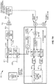
- FIG 3 depicts a method 1700 for configuring the operation of the power management system 870 ( Figure 2A ).
- the power management system 870 may determine an expected output power to be generated by a radio frequency power amplifier 869 ( Figure 2A ) during a data transmission. (Step 1702).
- the controller 50 ( Figure 2A ) may determine the expected output power to be generated by the radio frequency power amplifier 869 ( Figure 2A ) based upon the envelope characteristics of a data signal to be transmitted during a data transmission slot.
- the digital baseband processing portion of the transceiver or modem that provides the differential V RAMP signal to the parallel amplifier circuit 874 ( Figure 2A ) may determine the expected output power to be generated by the radio frequency power amplifier 869 ( Figure 2A ).
- the power management system 870 may select a power modulation mode of operation from among a number of power level modulation modes of operation. (Step 1704).
- the power management system 870 includes the high power modulation mode, the medium power modulation mode, and the low power average power tracking mode.
- the power management system 870 selects the one of the high power modulation mode, the medium power modulation mode, and the low power average power tracking mode.
- the power management system 870 configures the power management system 870 ( Figure 2A ) to operate in the high power modulation mode.
- the power management system 870 configures the power management system 870 ( Figure 2A ) to operate in the medium power modulation mode.
- the power management system 870 may configure the power management system 870 ( Figure 2A ) to operate in the medium power average power tracking mode. (Step 1710). In the case where the expected output power to be generated by the radio frequency power amplifier 869 ( Figure 2A ) is less than the low power modulation mode threshold, the power management system 870 ( Figure 2A ) may configure the power management system 870 ( Figure 2A ) to operate in the low power average power tracking mode. (Step 1712).
- the power management system 870 in another embodiment of the power management system 870 ( Figure 2A ), in the case where the expected output power to be generated by the radio frequency power amplifier 869 ( Figure 2A ) is less than the medium power modulation mode threshold, the power management system 870 ( Figure 2A ) may configure the power management system 870 ( Figure 2A ) to operate in the low power average power tracking mode (Step 1712).
- the high power modulation mode threshold is equal to about three decibels less than a maximum expected output power from the radio frequency power amplifier 869 ( Figure 2A ). In one embodiment of the power management system 870 ( Figure 2A ), the medium power modulation mode threshold is equal to about ten decibels less than a maximum expected output power from the radio frequency power amplifier 869 ( Figure 2A ).
- Figure 5 depicts a portion of a communication device including various embodiments of an envelope tracking modulated power supply system 2500 with transceiver power control loop compensation.
- the envelope tracking modulated power supply system 2500 with transceiver power control loop compensation may be described with continuing reference to a number of the embodiments of the pseudo-envelope tracking modulated power supply system 868, depicted in Figures 2A-C .
- the envelope tracking modulated power supply system 2500 with transceiver power control loop compensation may include a transceiver power control loop 2502 and an envelope tracking control system 2503.
- the transceiver power control loop 2502 may include a transmit-target power setting parameter 2502A and a transmit-gain setting parameter 2502B.
- the transceiver power control loop 2502 may adjust a drive level or an input power P IN of a modulated radio frequency input signal 2504 provided to a radio frequency power amplifier 2540 based on the values of the transmit-target power setting parameter 2502A and the transmit-gain setting parameter 2502B as a function of the output power P OUT generated by the radio frequency power amplifier 2540.
- the modulated radio frequency input signal 2504, P IN may be a test signal.
- the modulated radio frequency input signal 2504, P IN may be a carrier wave having a desired frequency.
- the transmit-target power setting parameter 2502A may be based on network control information provided by a communication network in which the communication device is configured to operate.
- the communication network may provide the communication device with network control information to configure the operation of the communication device within the communication network.
- the transmit-target power setting parameter 2502A used by a communication device may be a function of the different wireless transmissions generated by the communication device.
- the transmit-target power setting parameter 2502A of the communication device may also be based on a data rate of the transmission, the resource blocks to be used during the transmission, a frequency band allocated for the transmission, the relative location of the transmission band to other bands of operation in the communication network, and/or a combination thereof.
- the transmit-target power setting parameter 2502A may be a function of the distance between the communication device and a nearest base station of the communication network.
- the communication device may use an initial value of the transmit-target power setting parameter 2502A based on a target base station to receive an initial transmission. Thereafter, the communication network may configure the communication device to use a new value of the transmit-target power setting parameter 2502A based on a serving base station.
- the transceiver power control loop 2502 may adjust the transmit-gain setting parameter 2502B in response to changes in bias settings of the transceiver circuitry 2512, a temperature change of the digital baseband circuit 2510, and/or changes in the voltage standing wave ratio, VSWR, for a particular transmit frequency.
- the transceiver power control loop 2502 may be configured to adjust a transmit-gain setting parameter 2502B to provide a modulated radio frequency input signal 2504 to a radio frequency power amplifier 2540.
- the transmit-gain setting parameter 2502B may be adjusted as a function of the output power P OUT of the amplified radio frequency output signal 2548 provided to the antenna 2544 and the transmit-target power setting parameter 2502A.
- the transceiver power control loop 2502 may increase the transmit-gain setting parameter 2502B used to set the input power P IN of the modulated radio frequency input signal 2504 provided to the radio frequency power amplifier 2540 in response to a decrease in the output power P OUT of an amplified radio frequency output signal 2548 provided to the antenna 2544.
- the transceiver circuitry 2512 may increase the drive level of the modulated radio frequency input signal 2504 provided to the radio frequency power amplifier 2540.
- the transceiver circuitry 2512 may increase the input power P IN of the modulated radio frequency input signal 2504 to increase the output power P OUT of the amplified radio frequency output signal 2548.
- the envelope tracking control system 2503 may be configured to increase the amplitude of the modulated power supply voltage, V CC , provided to the collector of the radio frequency power amplifier 2540. Otherwise, the modulated power supply voltage, V CC , may be insufficient to support the increased output power P OUT to be generated by the radio frequency power amplifier 2540. Gain compression may result in degradation of the spectrum performance and the error vector magnitude (EVM) performance of the transmitted signal as measured at the output of the radio frequency power amplifier 2540.
- EVM error vector magnitude
- Figure 4 depicts a set of iso-gain contours of the radio frequency power amplifier 2540 that may be stored in a V CC look up table 2586, and used to generate the modulated power supply voltage, V CC , provided to the collector of the radio frequency power amplifier 2540.
- the sets of iso-gain contours may depict an iso-gain curve for the power gains 28dBm, 27dBm, 26dBm, and 25dBm.
- Figure 4 depicts an original input power P IN or drive level of a modulated radio frequency input signal provided as an input to the radio frequency power amplifier 2540 to transmit a data signal.
- Figure 4 further depicts an original range of the modulated power supply voltage, V CC , generated by the envelope tracking power converter system 2530 as a function of the digital I/Q signal 2506 provided to a digital baseband circuit 2510 for transmission.
- the modulated radio frequency input signal 2504 may also be generated based on the digital I/Q signal 2506.
- Figure 4 further depicts a new range of the modulated power supply voltage, V CC , that should be generated by the envelope tracking power converter system 2530 in response to the input power P IN of a modulated radio frequency input signal being increased by 1 dBm while maintaining the same modulation range.
- the modulated radio frequency input signal may cause the radio frequency power amplifier 2540 to change from the iso-gain contour for 27dBm of power gain to the iso-gain contour for 26dBm for an input power P IN or drive level above 6dBm.
- the radio frequency power amplifier 2540 may operate in a non-linear mode and jump from one iso-gain contour to another during the data transmission. This may result in gain compression.
- the envelope tracking control system 2503 may determine whether the transceiver power control loop 2502 has increased the drive level of the modulated radio frequency input signal, such that the envelope tracking power converter system 2530 may not be able to provide a sufficient range for the modulated power supply voltage, V CC , to support the increase in drive level. In that case, the envelope tracking control system 2503 may configure the digital baseband circuit 2510 to generate a control signal 2508 that will support the new range of the modulated power supply voltage, V CC , necessary to prevent gain compression.
- the transceiver power control loop 2502 may be further configured to cooperatively operate with the envelope tracking control system 2503.
- the envelope tracking control system 2503 may provide the control signal 2508 to the envelope tracking power converter system 2530 as a function of the digital I/Q signal 2506 provided to the digital baseband circuit 2510 for transmission.
- the digital I/Q signal 2506 may include a digital in-phase component I DIGITAL 2506A and a digital quadrature component Q DIGITAL 2506B.
- the envelope tracking control system 2503 may be configured to adjust the control signal 2508 as a function of the transmit-gain setting parameter 2502B, the transmit-target power setting parameter 2502A, a temperature measurement of the digital baseband circuit 2510, and/or some combination thereof.
- the envelope tracking control system 2503 may be further configured to adjust the control signal 2508 as a function of the transmit frequency of the transmitter channel for the band of operation in which the communication device is configured to operate.
- the envelope tracking control system 2503 may adjust the generation of a modulated power supply voltage, V CC , as a function of a transmit-target power setting parameter 2502A and a transmit-gain setting parameter 2502B, and a transmit frequency of the transmitter channel.
- Figure 5 may further depict an embodiment of a system, circuitry, and methods for providing a transceiver power control loop 2502 configured to regulate the output power P OUT of an amplified radio frequency output signal 2548 provided to the antenna 2544 in response to the modulated radio frequency input signal 2504.
- Figure 5 depicts the envelope tracking modulated power supply system 2500 with transceiver power control loop compensation including a digital baseband circuit 2510, an envelope tracking power converter system 2530, a radio frequency power amplifier 2540, a radio frequency switch 2542 in combination with an antenna 2544 and power coupler 2546.
- the digital baseband circuit 2510, the envelope tracking power converter system 2530, the radio frequency power amplifier 2540, and radio frequency switch 2542 may be in communication with a controller 50 via a control bus 44.
- the controller 50 may control and/or provide parameters to govern the function of the digital baseband circuit 2510, the envelope tracking power converter system 2530, the radio frequency power amplifier 2540, and the radio frequency switch 2542 by selectively setting parameters and settings in the various devices.
- the controller 50 may also provide a transmit-target power setting parameter 2502A to the digital baseband circuit 2510 as output power level control information received by the envelope tracking modulated power supply system 2500 from a base station of a communication network in which the envelope tracking modulated power supply system 2500 is configured to operate.
- the transmit-target power setting parameter 2502A may configure the digital baseband circuit 2510 to provide a modulated radio frequency input signal 2504 having an input power P IN to the radio frequency power amplifier 2540.
- the digital baseband circuit 2510 may be configured to receive the digital I/Q signal 2506 to be transmitted by the radio frequency power amplifier 2540 during a data transmission
- the digital I/Q signal 2506 may include a digital in-phase component I DIGITAL 2506A and a digital quadrature component Q DIGITAL 2506B.
- the digital baseband circuit 2510 may include transceiver circuitry 2512 and configuration-feedback circuitry 2520.
- the transceiver circuitry 2512 may include a front-end control interface circuit 2514 configured to communicate via a front-end control interface 2514A to the envelope tracking power converter system 2530.
- the digital baseband circuit 2510 may also configure various operational parameters of the envelope tracking power converter system 2530 via the front-end control interface 2514A.
- the digital baseband circuit 2510 may provide various operational parameters via the front-end control interface 2514A to the envelope tracking power converter system 2530 as a function of a regulated time period.
- the transceiver circuitry 2512 may provide a control signal 2508 to the envelope tracking power converter system 2530.
- the control signal 2508 may be a differential control signal having a non-inverted control signal component 2508A and an inverted control signal component 2508B.
- the control signal 2508 may be a differential V RAMP signal having a non-inverted V RAMP signal component and an inverted V RAMP signal component.
- the control signal 2508 may provide a target voltage for the modulated power supply voltage, V CC , at the modulated power supply output 876.
- the envelope tracking power converter system 2530 may generate a modulated power supply voltage, V CC , at the modulated power supply output 876.
- the transceiver circuitry 2512 may further include a temperature sensor 2516 configured to provide a temperature measurement of the digital baseband circuit 2510.
- the transceiver circuitry 2512 may also include a feedback analog-to-digital converter 2518 configured to receive a measurement signal 2532 from the envelope tracking power converter system 2530.
- the measurement signal 2532 in combination with the feedback analog-to-digital converter 2518 may provide information such as the temperature and supply voltage of the envelope tracking power converter system 2530.
- the feedback analog-to-digital converter 2518 may receive the measurement signal 2532 from the envelope tracking power converter system 2530.
- the feedback analog-to-digital converter 2518 may convert the measurement signal 2532 into digital data, which may be provided to the controller 50 or other portions of the digital baseband circuit 2510.
- the envelope tracking power converter system 2530 may provide various types of measurements, including an analog temperature signal, an analog power supply voltage signal, and a measurement of the battery voltage, V BAT .
- the digital baseband circuit 2510 may request the envelope tracking power converter system 2530 to provide a measurement of the battery voltage, V BAT , from a battery 20.
- the envelope tracking power converter system 2530 may provide a measurement of the battery voltage, V BAT , to the feedback analog-to-digital converter 2518 via the measurement signal 2532.
- the digital baseband circuit 2510 may obtain a measurement of the temperature of the envelope tracking power converter system 2530 via the measurement signal 2532.
- the transceiver circuitry 2512 may generate a control signal 2508 to provide a target voltage for generation of a modulated power supply voltage, V CC .
- the control signal 2508 may be a differential V RAMP signal.
- the envelope tracking power converter system 2530 may configure the digital baseband circuit 2510 to generate the control signal 2508 as a function of the modulated radio frequency input signal 2504 provided to the radio frequency power amplifier 2540 for transmission.
- the envelope tracking power converter system 2530 may generate the modulated power supply voltage, V CC , at the modulated power supply output 876 in response to the control signal 2508.
- the envelope tracking power converter system 2530 may provide the modulated power supply voltage, V CC , to the radio frequency power amplifier 2540.
- the radio frequency power amplifier 2540 may generate an amplified radio frequency output signal 2548 as a function of the input power P IN of the modulated radio frequency input signal 2504 and the modulated power supply voltage V CC .
- the radio frequency power amplifier 2540 may provide the amplified radio frequency output signal 2548 to the antenna 2544 via a radio frequency switch 2542.
- the power coupler 2546 may obtain a measurement of the amplified radio frequency output signal 2548. In some embodiments, the power coupler 2546 may also obtain a measurement of the output power of the amplified radio frequency output signal 2548, present at the antenna 2544. In other embodiments of the transceiver power control loop 2502, the power coupler 2546 may be located at the output of the radio frequency power amplifier 2540 and configured to obtain a measurement of the amplified radio frequency output signal 2548 before passing through the radio frequency switch 2542. Some embodiments of the power coupler 2546 may include a power detector configured to measure the output power P OUT of the amplified radio frequency output signal 2548 at the output of the radio frequency power amplifier 2540.
- the power coupler 2546 may provide a measured amplified radio frequency output signal 2550 to the digital baseband circuit 2510.
- the power coupler 2546 may provide the measured amplified radio frequency output signal 2550 to the configuration-feedback circuitry 2520 of the digital baseband circuit 2510.
- the I/Q feedback system 2522 may receive the measured amplified radio frequency output signal 2550.
- the I/Q feedback system 2522 may demodulate the measured amplified radio frequency output signal 2550 to obtain a digitized in-phase feedback component I MEASURED 2570 and a digitized quadrature feedback component Q MEASURED 2572 as a function of the measured amplified radio frequency output signal 2550.
- the digitized in-phase feedback component I MEASURED 2570 and the digitized quadrature feedback component Q MEASURED 2572 may be provided to the fast calibration iso-gain and delay alignment circuitry 2524 and the transceiver power control loop circuitry 2526.
- the transceiver power control loop circuitry 2526 also receives the transmit-target power setting parameter 2502A. Based on the digitized in-phase feedback component I MEASURED 2570 and the digitized quadrature feedback component Q MEASURED 2572, the transceiver power control loop circuitry 2526 may determine whether to increase or decrease the power level of the modulated radio frequency input signal 2504 as a function of the transmit-target power setting parameter 2502A.
- the transceiver power control loop circuitry 2526 may determine that the output power P OUT of the measured amplified radio frequency output signal 2550 is less than the transmit-target power setting parameter 2502A. In response to the determination that the output power P OUT of the measured amplified radio frequency output signal 2550 is less than the transmit-target power setting parameter 2502A, the transceiver power control loop circuitry 2526 may configure the transceiver circuitry 2512 to increase the input power P IN of the modulated radio frequency input signal 2504 provided to the radio frequency power amplifier 2540. For example, in some embodiments, the transceiver power control loop circuitry 2526 may increase the magnitude of the transmit-gain setting parameter 2502B.
- the transceiver power control loop circuitry 2526 may generate a transmit-gain setting signal 2526A based on the transmit-gain setting parameter 2502B. In some embodiments, the transceiver power control loop circuitry 2526 may provide the transmit-gain setting signal 2526A to a baseband controller 2511.
- the baseband controller 2511 may be configured to adjust various parameters and settings of the transceiver circuitry 2512 to increase the drive level or input power P IN of the modulated radio frequency input signal 2504 to compensate for the difference between the transmit-target power setting parameter 2502A and the output power P OUT of the measured amplified radio frequency output signal 2550.
- the transceiver power control loop circuitry 2526 may provide the transmit-gain setting signal 2526A and a transmit-target power setting signal 2526B to a pseudo-envelope follower gain control circuit 2574.
- the baseband controller 2511 may provide the transmit-gain setting parameter 2502B and a transmit-target output power parameter to the pseudo-envelope follower gain control circuit 2574.
- the baseband controller 2511 may configure the pseudo-envelope follower gain control circuit 2574 to generate a gain control signal 2574A having a gain control magnitude substantially equal to G CONTROL .
- the transceiver power control loop circuitry 2526 may determine that the output power P OUT of the measured amplified radio frequency output signal 2550 exceeds the transmit-target power setting parameter 2502A. Based on a determination that the output power P OUT of the measured amplified radio frequency output signal 2550 exceeds the transmit-target power setting parameter 2502A, the transceiver power control loop circuitry 2526 may decrease the magnitude of the transmit-gain setting parameter 2502B.
- the transceiver power control loop circuitry 2526 may generate a transmit-gain setting signal 2526A based on the reduced magnitude of the transmit-gain setting parameter 2502B.
- the baseband controller 2511 may be configured to adjust various parameters and settings of the transceiver circuitry 2512 to reduce the drive level or input power P IN of the modulated radio frequency input signal 2504 to decrease the output power P OUT of the measured amplified radio frequency output signal 2550.
- the transceiver power control loop circuitry 2526 may provide the transmit-gain setting signal 2526A to the pseudo-envelope follower gain control circuit 2574.
- the power coupler 2546 may include a detector.
- the detector may include a sensor in communication with an output of the radio frequency power amplifier 2540.
- the detector may measure an output power generated by the radio frequency power amplifier 2540.
- the power coupler 2546 may provide a measured output power, P OUT , of the amplified radio frequency output signal 2548.
- the measured output power may provide an average power measurement.
- the power coupler 2546 may also provide an average power measurement based on various averaging techniques.
- the power coupler 2546 may be configured to provide a peak power measurement.
- the power coupler 2546 may be configured as a linear power detector.
- the power coupler 2546 may be a logarithmic power detector.
- the power coupler 2546 may be a non-linear power detector.
- the radio frequency switch 2542 includes a closed state of operation and an open state of operation.
- the radio frequency switch 2542 may couple the radio frequency power amplifier 2540 to the antenna 2544, which permits the amplified radio frequency output signal 2548 to pass through the radio frequency switch 2542 to the antenna 2544 to transmit the amplified radio frequency output signal 2548.
- the radio frequency switch 2542 substantially attenuates the amplified radio frequency output signal 2548 to minimize or prevent a transmission of the amplified radio frequency output signal 2548.
- the radio frequency switch 2542 has infinite impedance.
- the radio frequency switch 2542 may provide antenna switch isolation around +25 dBm.
- the communication device may include a controller 50 configured to coordinate the functions of the various components and operations of the embodiments of the envelope tracking modulated power supply system 2500 with transceiver power control loop compensation.
- the controller 50 may include a number of distributed processors, distributed microcontrollers, controllers, local control units, memory mapped local memory for various components, functions, and features of the various embodiments of the power management system 870, the various embodiments of the switch mode power supply converter 872, the various embodiments of the parallel amplifier circuit 874, firmware circuitry, reconfigurable digital logic circuitry, state machines, analog logic circuitry, a number of communication interfaces and busses, various forms of memory, data registers, control registers, cache memory, distributed memory, memory mappings, register mappings, various types of sensors and inputs for receiving sensory data or information, one or more digital-to-analog converters, one or more analog-to-digital converters, various types and numbers of output drivers, various types and numbers of digital input buffers and analog input buffers, various processor
- the controller 50 may be described as performing various functions and features to govern the operation of the communication device, the various embodiments of the envelope tracking modulated power supply system 2500 with transceiver power control loop compensation, the digital baseband circuit 2510, the envelope tracking power converter system 2530, the radio frequency power amplifier 2540, the radio frequency switch 2542, the power coupler 2546.
- the controller 50 may include a control bus 44 in communication with the digital baseband circuit 2510, the envelope tracking power converter system 2530, the radio frequency power amplifier 2540, the radio frequency switch 2542, and the power coupler 2546.
- the control bus 44 is only depicted as being in communication with each component depicted in Figure 1 . Even so, one of ordinary skill in the art will understand that this is by way of example and not by way of limitation.
- the controller 50 may be in communication with various other elements to be described in the digital baseband circuit 2510, the embodiments of the switch mode power supply converter 872, and the embodiments of the parallel amplifier circuit 874 of the envelope tracking power converter system 2530.
- the controller 50 may be in communication with and cooperatively operate with the various embodiments of the power management system 870.
- the controller 50 may include a processor, a Digital Signal Processor (DSP), an Application Specific Integrated Circuit (ASIC), a Field Programmable Gate Array (FPGA) or other programmable logic device, discrete gate or transistor logic, discrete hardware components, or any combination thereof designed to perform the functions described herein.
- a processor may be a microprocessor. In the alternative, the processor may be any conventional processor, controller, microcontroller, a state machine and/or a combination thereof.
- a processor may also be implemented as a combination of computing devices. As an example, a combination of computing devices may include a combination of a DSP and a microprocessor, a plurality of microprocessors, one or more microprocessors in conjunction with a DSP core, or any other such configuration.
- the processor 28 may further include or be embodied in hardware and in computer executable instructions that are stored in memory, and may reside, for example, in Random Access Memory (RAM), flash memory, Read Only Memory (ROM), Electrically Programmable ROM (EPROM), Electrically Erasable Programmable ROM (EEPROM), registers, hard disk, a removable disk, a CD-ROM, or any other form of computer readable medium known in the art.
- RAM Random Access Memory
- ROM Read Only Memory
- EPROM Electrically Programmable ROM
- EEPROM Electrically Erasable Programmable ROM
- registers hard disk, a removable disk, a CD-ROM, or any other form of computer readable medium known in the art.
- An exemplary storage medium may be coupled to the processor such that a processor can read information from, and write information to, the storage medium.
- the storage medium or a portion of the storage medium may be integral to the processor.
- the processor and the storage medium may reside in an Application Specific Integrated Circuit (ASIC).
- ASIC Application Specific Integrated
- the front-end control interface circuit 2514 is in communication with the envelope tracking power converter system 2530 via a front-end control interface 2536.
- the front-end control interface circuit 2514 may operate with a Mobile Industry Processor Interface® standard based device via the front-end control interface 2536.
- the front-end control interface circuit 2514 and the front-end control interface 2536 may be configured to control devices based on a Radio Frequency Front-End control interface specification.
- the controller 50 may cooperatively interoperate the front-end control interface circuit 2514 to configure and control the envelope tracking power converter system 2530.
- the controller 50 may be a supervisory processor that governs other controllers.
- the baseband controller 2511 may include configurable firmware, a processor, sub-controllers, control logic, control circuitry, one or more state machines, a Digital Signal Processor (DSP), an ASIC, a Field Programmable Gate Array (FPGA) or other programmable logic device, discrete gate or transistor logic, discrete hardware components, or any combination thereof designed to perform the functions described herein.
- DSP Digital Signal Processor
- FPGA Field Programmable Gate Array
- the baseband controller 2511 may include firmware, executable program code, read only memory, fusible memory, a memory processor, a microprocessor, conventional processor, controller, microcontroller, or state machine.
- a processor may also be implemented as a combination of computing devices.
- a combination of computing devices may include a combination of a DSP and a microprocessor, a plurality of microprocessors, one or more microprocessors in conjunction with a DSP core, or any other such configuration.
- the controller 50 may further include or be embodied in hardware and in computer executable instructions that are stored in memory, and may reside, for example, in Random Access Memory (RAM), flash memory, Read Only Memory (ROM), Electrically Programmable ROM (EPROM), Electrically Erasable Programmable ROM (EEPROM), registers, hard disk, a removable disk, a CD-ROM, or any other form of computer readable medium known in the art.
- RAM Random Access Memory
- ROM Read Only Memory
- EPROM Electrically Programmable ROM
- EEPROM Electrically Erasable Programmable ROM
- registers hard disk, a removable disk, a CD-ROM, or any other form of computer readable medium known in the art.
- An exemplary storage medium may be coupled to the processor such that a processor can read information from, and write information to, the storage medium.
- the storage medium or a portion of the storage medium may be integral to the processor.
- the processor and the storage medium may reside in an Application Specific Integrated Circuit (ASIC).
- ASIC Application Specific Integrated
- the digital baseband circuit 2510 may receive a digital I/Q signal 2506 to be transmitted by the radio frequency power amplifier 2540.
- the digital I/Q signal 2506 includes a digital data signal.
- the digital I/Q signal 2506 may be a test signal for calibrating various parts of the envelope tracking modulated power supply system 2500 with transceiver power control loop compensation.
- the digital I/Q signal 2506 may include a digital in-phase component I DIGITAL 2506A and a digital quadrature component Q DIGITAL 2506B.
- the digital I/Q signal 2506 may receive various types of test signals to generate a modulated radio frequency input signal 2504 having a desired envelope characteristic.
- the digital I/Q signal 2506 may include a test signal that generates the modulated radio frequency input signal 2504 having a desired frequency characteristic or periodicity.
- the test signal received by the digital I/Q signal 2506 may include various frequency characteristics.
- the digital I/Q signal 2506 may generate a modulated radio frequency input signal 2504 that has a bandwidth substantially similar to the bandwidth associated with the wideband modulation technique or the band of operation assigned to the communication device.
- the digital baseband circuit 2510 may further include a pseudo-envelope follower gain control circuit 2574 configured to provide a gain control signal 2574A having a gain control magnitude substantially equal to G CONTROL .
- the pseudo-envelope follower gain control circuit 2574 may adjust the magnitude of the gain control signal 2574A based as a function of a measured temperature of the transceiver circuitry 2512, the transmit-gain setting signal 2526A, a carrier frequency for the band of operation in which the communication device is configured to operate, and/or a combination thereof to generate the V CC look up table index signal 2584 at the input of the V CC look up table 2586.
- the pseudo-envelope follower gain control circuit 2574 may adjust the gain control magnitude, G CONTROL , such that the V CC look up table index signal 2584 provides an index signal into the V CC look up table 2586 that substantially emulates the drive level or input power P IN of the modulated radio frequency input signal 2504 provided to the radio frequency power amplifier 2540.
- the pseudo-envelope follower gain control circuit 2574 may adjust the magnitude of the gain control magnitude, G CONTROL , such that the V CC look up table compensated envelope signal 2588 may provide a target voltage for the modulated power supply voltage, V CC , as a function of the iso-gain curve that corresponds to the transmit-target power setting parameter 2502A.
- the gain control signal 2574A may compensate for an increase in the input power of the modulated radio frequency input signal provided to the radio frequency power amplifier 2540 to prevent or minimize gain compression.
- the envelope tracking power converter system 2530 may include various circuits to generate a modulated power supply voltage, V CC , at the modulated power supply output 876.
- some embodiments of the envelope tracking power converter system 2530 may include the switch mode power supply converter 872 and the parallel amplifier circuit 874.
- the switch mode power supply converter 872 may be a buck converter.
- the switch mode power supply converter 872 may include a multi-level charge pump buck converter configured to buck and/or boost a supply voltage to provide a switching voltage at different voltages dependent upon the control signal 2508.
- the envelope tracking power converter system 2530 may operate in various power level modulation modes depending on the expected output power to be generated by the radio frequency power amplifier 2540 in a data transmission.
- the transceiver circuitry 2512 may include an AM/PM compensation circuit 2573, a digital gain control circuit 2576, an envelope magnitude calculation circuit 2578, and an envelope tracking digital/analog section 2580.
- the envelope magnitude calculation circuit 2578 may receive the digital in-phase component I DIGITAL 2506A and the digital quadrature component Q DIGITAL 2506B.
- the envelope magnitude calculation circuit 2578 may calculate an envelope magnitude, ⁇ MAGNITUDE , of an expected envelope of the modulated radio frequency input signal 2504, P IN .
- the envelope magnitude calculation circuit 2578 may generate the envelope magnitude, ⁇ MAGNITUDE , based on the digital in-phase component I DIGITAL 2506A and the digital quadrature component Q DIGITAL 2506B.
- the envelope magnitude, ⁇ MAGNITUDE may be proportional to the magnitude of the envelope of the modulated radio frequency input signal 2504, P IN .
- the envelope magnitude calculation circuit 2578 provides the envelope magnitude, ⁇ MAGNITUDE , to the envelope tracking digital/analog section 2580.
- the AM/PM compensation circuit 2573 may be configured to receive the digital in-phase component I DIGITAL 2506A and the digital quadrature component Q DIGITAL 2506B. In some embodiments, the AM/PM compensation circuit 2573 may be configured to provide amplitude modulation and phase modulation compensation for the radio frequency power amplifier 2540. For example, some embodiments of the AM/PM compensation circuit 2573 may adjust the digital in-phase component I DIGITAL 2506A and the digital quadrature component Q DIGITAL 2506B to compensate for any phase shift due to the modulated power supply voltage, V CC , the input power, P IN , of the modulated radio frequency input signal 2504 to be transmitted by the radio frequency power amplifier 2540, and/or a combination thereof.
- the AM/PM compensation circuit 2573 may receive the V CC look up table index signal 2584 and the V CC look up table compensated envelope signal 2588.
- the V CC look up table index signal 2584 may be substantially equivalent to a digital representation of the envelope of the modulated radio frequency input signal 2504 provided to the radio frequency power amplifier 2540 for transmission.
- the V CC look up table compensated envelope signal 2588 may be substantially equivalent to a digital representation of a target envelope for the envelope tracking power converter system 2530 to track or follow to generate a modulated power supply voltage, V CC , that substantially corresponds to the modulated radio frequency input signal 2504.
- the V CC look up table 2586 may translate the V CC look up table index signal 2584 into a desired target voltage for the modulated power supply voltage, V CC .
- the pseudo-envelope follower gain control circuit 2574 may generate the gain control, G CONTROL , signal as a function of a temperature of the digital baseband circuit 2510, the transmit-target power setting signal 2526B, the transmit-gain setting signal 2526A, and/or a combination thereof to adjust the magnitude of the envelope magnitude, ⁇ MAGNITUDE , signal.
- the V CC look up table index signal 2584 may include a transceiver gain adjusted envelope magnitude ⁇ TGA-MAGNITUDE , substantially equal to the product of the envelope magnitude, ⁇ MAGNITUDE , signal and the gain control, G CONTROL , signal.
- the gain control, G CONTROL adjusts the envelope magnitude, ⁇ MAGNITUDE , signal to reflect a change in the transceiver gain such that the V CC look up table index signal is not solely based on the expected output power to be generated by the radio frequency power amplifier 2540 in response to the modulated radio frequency input signal 2504.
- the V CC look up table index signal 2584 substantially compensates for a change in the gain of the digital transceiver to reflect the input drive level to the radio frequency power amplifier.
- the V CC look up table index signal 2584 provides an emulated "Pin drive level of the power amplifier" rather using as index the output power of the radio frequency power amplifier 2540 to generate the control signal 2508.
- the V CC look up table index signal 2584 may index into the V CC look up table 2586 to generate a V CC look up table compensated envelope signal 2588 that is adjusted for a change in the transmit-gain setting signal 2526A used to set the power level of the modulated radio frequency input signal 2504 provided to the radio frequency power amplifier 2540.
- the AM/PM compensation circuit 2573 may compensate for any phase shift due to the drive level change in of the modulated radio frequency input signal 2504 provided to the radio frequency power amplifier 2540.
- the AM/PM compensation circuit 2573 may receive either the V CC look up table index signal 2584 or the V CC look up table compensated envelope signal 2588 as a scaled version of the digital envelope of the modulated radio frequency input signal 2504. In other words, the AM/PM compensation circuit 2573 may use either the V CC look up table index signal 2584, the V CC look up table compensated envelope signal 2588, and/or a combination thereof to represent the modulated radio frequency input signal 2504. Based on the representation of the modulated radio frequency input signal 2504, the AM/PM compensation circuit 2573 may calculate a phase correction as a function of the input power P IN .
- the AM/PM compensation circuit 2573 may apply the phase correction to generate a phase corrected digital in-phase component I DIGITAL 2573I and a phase corrected digital in-phase component I- DIGITAL 2527Q, which are provide to the digital gain control circuit 2576.
- the digital gain control circuit 2576 may generate a gain adjusted digital in-phase, I DIGITAL-_GAIN_ADJUSTED , component and the gain adjusted digital quadrature, Q DIGITAL_GAIN_ADJUSTED , component based on the transmit-gain setting parameter 2502B.
- the envelope tracking digital/analog section 2580 may include the pseudo-envelope follower gain control circuit 2574, a multiplier 2582, the V CC look up table 2586, a fine tuning delay circuit 2590, a digital pre-distortion compensation filter 2594, a differential digital-to-analog converter 2598, and a fixed delay circuit 2600.
- the multiplier 2582 may include a first input in communication with the output of the pseudo-envelope follower gain control circuit 2574 and a second input in communication with the envelope magnitude calculation circuit 2578. The first input of the multiplier 2582 may receive the gain control, G CONTROL , from the pseudo-envelope follower gain control circuit 2574.
- the second input of the multiplier 2582 may receive the envelope magnitude, ⁇ MAGNITUDE .
- the multiplier 2582 multiplies the envelope magnitude, ⁇ MAGNITUDE , by the gain control, G CONTROL , to generate the V CC look up table index signal 2584.
- the gain control, G CONTROL is adjusted to compensate for variations in a setup of the digital baseband circuit 2510.
- the value of the gain control, G CONTROL may be adjusted to increase or decrease the modulated power supply voltage, V CC , generated by the envelope tracking power converter system 2530 as a function of the input power P IN or drive level of the modulated radio frequency input signal 2504 provided to the radio frequency power amplifier 2540.
- the multiplier 2582 provides a V CC look up table index signal 2584 to the V CC look up table 2586 based on the product of the envelope magnitude, ⁇ MAGNITUDE , and the gain control, G CONTROL .
- the V CC look up table 2586 may include one or more tables to translate the V CC look up table index signal 2584 into a V CC look up table compensated envelope signal 2588.
- the V CC look up table compensated envelope signal 2588 may provide a target voltage for the modulated power supply voltage, V CC , to be generated by the envelope tracking power converter system 2530 based on the envelope of the modulated radio frequency input signal 2504.
- the baseband controller 2511 or the controller 50 may configure the V CC look up table 2586 to select a particular set of look up values as a function of an operational mode of the communication device, the digital baseband circuit 2510, the envelope tracking power converter system 2530, the envelope tracking digital/analog section 2580, and/or a combination thereof.
- the V CC look up table 2586 provides a V CC look up table compensated envelope signal 2588 to the fine tuning delay circuit 2590.
- the fine tuning delay circuit 2590 may be configured to delay propagation of the V CC look up table compensated envelope signal 2588 based on a programmable delay parameter.
- the programmable delay parameter may be controlled by the controller 50 the baseband controller 2511 and/or a combination thereof.
- the fine tuning delay circuit 2590 may provide a delay propagation of the V CC look up table compensated envelope signal 2588 based on a programmable delay parameter by a fine tuning delay time, T FINE_TUNING .
- the granularity of the fine tuning delay time, T FINE_TUNING may depend upon a clock of the digital baseband circuit 2510.
- the propagation delay of the fine tuning delay circuit 2590 may be provided by an interpolator.
- the propagation delay of the fine tuning delay circuit 2590 may be provided by a tapped delay line or other delay circuit.
- the fine tuning delay circuit 2590 provides a digitally delayed control signal without pre-distortion compensation 84 to the digital pre-distortion compensation filter 2594.
- the digitally delayed control signal without pre-distortion compensation 84 may be provided to the digital pre-distortion compensation filter 2594.
- the digital pre-distortion compensation filter 2594 may be either an infinite impulse response filter (IIR) or a finite impulse response filter (FIR).
- IIR infinite impulse response filter
- FIR finite impulse response filter
- the coefficients of the digital pre-distortion compensation filter 2594 may be configured by the controller 50, baseband controller 2511 and/or a combination thereof.
- the propagation delay through the digital pre-distortion compensation filter 2594 may vary depending upon the various modes of operation of the communication device.
- the propagation delay through the digital pre-distortion compensation filter 2594 may depend on various factors including a band of operation, a channel bandwidth, a wideband modulation bandwidth, channel conditions, a location of the communication device relative to communication hubs, points, towers, and hot-spots, signal modulation techniques, expected envelope characteristics, the peak-to-average ratio of the envelope of the signal to be transmitted, the data rate, the bandwidth of the channel, error vector magnitude, desired transmit spectrum characteristics, and/or some combination thereof.
- the digital pre-distortion compensation filter 2594 may be configured to equalize the frequency response of the modulated power supply voltage, V CC , relative to the differential V RAMP signal.
- the digital pre-distortion compensation filter 2594 may provide a digital control signal 2596 to the differential digital-to-analog converter 2598.
- the digital control signal 2596 may be a digital V RAMP signal, V RAMP_DIGITAL .
- the differential digital-to-analog converter 2598 may convert the digital control signal 2596 into the control signal 2508.
- the control signal 2508 may be a differential control signal.
- control signal 2508 may include the non-inverted control signal component 2508A and the inverted control signal component 2508B.
- the non-inverted control signal component 2508A may be the non-inverted V RAMP signal component, V RAMP +
- the inverted control signal component 2508B may be the inverted V RAMP signal component, V RAMP -.
- the differential digital-to-analog converter 2598 may further include anti-aliasing filters to accomplish proper image rejection after converting digital data into an analog signal.
- the fixed delay circuit 2600 may provide a fixed delay to offset the propagation delay of the of the envelope magnitude, ⁇ MAGNITUDE , signal through the envelope tracking digital/analog section 2580 and provide a range of delay for the fine tuning delay circuit 2590.
- the fixed delay circuit 2600 receives the gain adjusted digital in-phase, I DIGITAL_GAIN_ADJUSTED , component and the gain adjusted digital quadrature, Q DIGITAL_GAIN_ADJUSTED , component from the digital gain control circuit 2576.
- the fixed delay circuit 2600 provides a delay adjusted digital in-phase component 2604 and a delay adjusted quadrature component 2618 as outputs.
- a first digital-to-analog converter circuit 2606 is configured to receive the delay adjusted digital in-phase component 2604.
- the first digital-to-analog converter circuit 2606 converts the delay adjusted digital in-phase component 2604 into an analog signal to generate a pre-reconstruction in-phase component 2608, which is provided to a first anti-aliasing filter 2610.
- the first anti-aliasing filter 2610 filters the pre-reconstruction in-phase component 2608 to provide an analog in-phase component 2612 to be mixed.
- a second digital-to-analog converter circuit 2620 may receive the delay adjusted quadrature component 2618.
- the second digital-to-analog converter circuit 2620 converts the delay adjusted quadrature component 2618 into a pre-reconstruction quadrature component 2622, which is provided to a second anti-aliasing filter 2624.
- the second anti-aliasing filter 2624 filters the pre-reconstruction quadrature component 2622 to provide an analog quadrature component 2626 to be mixed.
- the digital baseband circuit 2510 may further include an oscillator 2558, an in-phase component mixer 2614, I-Mixer, and a quadrature component mixer 2628, Q-Mixer.
- the oscillator 2558 is configured to generate a carrier signal 2558A having a transmit carrier frequency for a band of operation, which is provided to the quadrature component mixer 2628, Q-Mixer, and the in-phase component mixer 2614, I-Mixer.
- the quadrature component mixer 2628, Q-Mixer mixes the analog quadrature component 2626 to generate a modulated quadrature component 2630.
- the in-phase component mixer 2614, I-Mixer mixes the analog in-phase component 2612 to generate a modulated in-phase component 2616.
- the modulated quadrature component 2630 and the modulated in-phase component 2616 are provided to a radio frequency attenuator 2632.
- the controller 50 may adjust the radio frequency attenuator 2632 to provide a magnitude of the modulated quadrature component 2630 and the modulated in-phase component 2616 used to provide the modulated radio frequency input signal 2504 having an input power P IN to the radio frequency power amplifier 2540.
- the radio frequency attenuator 2632 may be either a digital radio frequency attenuator or an analog radio frequency attenuator.
- the fine tuning delay time, T FINE_TUNING , of the fine tuning delay circuit 2590 may be configured to adjust the group delay relationship between the control signal 2508 provided to the envelope tracking power converter system 2530 and the modulated radio frequency input signal 2504, P IN , provided to the radio frequency power amplifier 2540.
- the output power of the amplified radio frequency output signal 2548 may depend on the relative group delay mismatch between the control signal 2508 and the modulated radio frequency input signal 2504, P IN .
- Figure 6 depicts a more detailed view of the digital baseband circuit 2510 including the baseband controller 2511, the transceiver circuitry 2512, and the configuration-feedback circuitry 2520. Although Figure 6 depicts that the transceiver circuitry 2512 and the configuration-feedback circuitry 2520 are substantially separate portions of the digital baseband circuit 2510, in some embodiments, the features and the functions of the transceiver circuitry 2512 and the configuration-feedback circuitry 2520 may be cooperatively shared.
- Figure 6 further depicts an I/Q feedback system 2522 having a buffer 2552 configured to receive the measured amplified radio frequency output signal 2550 from the power coupler 2546.
- the buffer 2552 provides the measured amplified radio frequency output signal 2550 to the in-phase component feedback mixer 2554 and the quadrature component feedback mixer 2556.
- the in-phase component feedback mixer 2554 and the quadrature component feedback mixer 2556 may receive a carrier signal 2558A having a transmit carrier frequency from an oscillator 2558.
- the in-phase component feedback mixer 2554 and the quadrature component feedback mixer 2556 may demodulate the measured amplified radio frequency output signal 2550 to recover an in-phase feedback component 2562 and a quadrature feedback component 2564.
- the in-phase component feedback mixer 2554 may provide the in-phase feedback component 2562 to an in-phase component analog-to-digital converter 2566 to generate a digitized in-phase feedback component I MEASURED 2570.
- the quadrature component feedback mixer 2556 may provide the quadrature feedback component 2564 to a quadrature component analog-to-digital converter 2568 to generate a digitized quadrature feedback component Q MEASURED 2572.
- the fast calibration iso-gain and delay alignment circuitry 2524 and the transceiver power control loop circuitry 2526 may each receive the digitized in-phase feedback component I MEASURED 2570 and the digitized quadrature feedback component Q MEASURED 2572.
- the V CC look up table 2586 may store a plurality of calibrated iso-gain contours.
- the iso-gain contours may be calibrated by measuring the relationship between a range of drive levels or input power P IN levels of a modulated radio frequency input signal 2504 versus an output power P OUT generated by the radio frequency power amplifier 2540 at a given modulated power supply voltage, V CC .
- the input power P IN for a modulated radio frequency input signal 2504 may sweep through 27dBn to + 7 dbm at a given modulated power supply voltage, Vcc.
- the fast calibration iso-gain and delay alignment circuitry 2524 may determine the output power generated in response to the input power P IN level. The process may then be repeated for different magnitudes of the modulated power supply voltage, V CC .
- the configuration-feedback circuitry 2520 regulates an output power from the radio frequency power amplifier 2540 based on a difference between a target output power from the radio frequency power amplifier 2540 and a measured output power from the radio frequency power amplifier 2540.
- the transceiver circuitry 2512 regulates the modulated power supply voltage, V CC , which is used by the radio frequency power amplifier 2540 to provide power for amplification, based on the difference between the target output power from the radio frequency power amplifier 2540 and the measured output power from the radio frequency power amplifier 2540.
- the configuration-feedback circuitry 2520 regulates the output power from the radio frequency power amplifier 2540, such that the measured output power from the radio frequency power amplifier 2540 is about equal to the target output power from the radio frequency power amplifier 2540.
- the transceiver circuitry 2512 provides the modulated radio frequency input signal 2504 having the input power P IN to the radio frequency power amplifier 2540.
- the radio frequency power amplifier 2540 generates the amplified radio frequency output signal 2548 as a function of the input power P IN of the modulated radio frequency input signal 2504 and the modulated power supply voltage V CC .
- the measured output power from the radio frequency power amplifier 2540 is representative of the output power from the radio frequency power amplifier 2540.
- the measured amplified radio frequency output signal 2550 is representative of the measured output power from the radio frequency power amplifier 2540.
- the transmit-gain setting signal 2526A is based on the transmit-gain setting parameter 2502B and the transmit-target power setting signal 2526B is based on the transmit-target power setting parameter 2502A.
- the transmit-target power setting parameter 2502A is representative of the target output power from the radio frequency power amplifier 2540 and the transmit-gain setting parameter 2502B is representative of the transmit-gain setting of the transceiver circuitry 2512.
- the configuration-feedback circuitry 2520 receives the measured amplified radio frequency output signal 2550 and provides the transmit-gain setting parameter 2502B based on the measured amplified radio frequency output signal 2550 and the transmit-target power setting parameter 2502A.
- the transmit-gain setting signal 2526A is based on the measured amplified radio frequency output signal 2550 and the transmit-target power setting parameter 2502A.
- the transceiver circuitry 2512 adjusts the input power P IN of the modulated radio frequency input signal 2504 provided to the radio frequency power amplifier 2540 based on the values of the transmit-target power setting parameter 2502A and the transmit-gain setting parameter 2502B. In one embodiment of the transceiver circuitry 2512, the transceiver circuitry 2512 adjusts the transmit-gain setting parameter 2502B in response to changes in bias settings of the transceiver circuitry 2512. In one embodiment of the transceiver circuitry 2512, the transceiver circuitry 2512 adjusts the transmit-gain setting parameter 2502B in response to temperature changes of the transceiver circuitry 2512.
- the transceiver circuitry 2512 adjusts the transmit-gain setting parameter 2502B in response to changes in the voltage standing wave ratio, VSWR associated with the radio frequency power amplifier 2540. In one embodiment of the transceiver circuitry 2512, the transceiver circuitry 2512 adjusts the transmit-gain setting parameter 2502B in response to changes in a transmit frequency of the radio frequency power amplifier 2540.
- the envelope tracking power converter system 2530 generates the modulated power supply voltage, V CC , at the modulated power supply output 876 based on the control signal 2508.
- the modulated power supply voltage, V CC is based on the control signal 2508.
- the transceiver circuitry 2512 receives the digital I/Q signal 2506.
- the digital I/Q signal 2506 is an I/Q signal.
- the modulated power supply voltage, V CC is based on the I/Q signal and the modulated radio frequency input signal 2504, which is provided to the radio frequency power amplifier 2540, is also based on the I/Q signal.
- the transceiver circuitry 2512 adjusts the modulated power supply voltage, V CC , via the control signal 2508 to compensate for changes of the transmit-gain setting of the transceiver circuitry 2512.
- the modulated power supply voltage, V CC is based on the V CC look up table 2586, such that the V CC look up table index signal 2584 provides an index signal into the V CC look up table 2586 that substantially emulates the input power P IN of the modulated radio frequency input signal 2504 provided to the radio frequency power amplifier 2540.
- the transceiver circuitry 2512 adjusts the V CC look up table index signal 2584 in response to changes of the transmit-gain setting of the transceiver circuitry 2512.
- the transceiver circuitry 2512 adjusts the V CC look up table index signal 2584 in response to changes in bias settings of the transceiver circuitry 2512. In one embodiment of the transceiver circuitry 2512, the transceiver circuitry 2512 adjusts the V CC look up table index signal 2584 in response to temperature changes of the transceiver circuitry 2512. In one embodiment of the transceiver circuitry 2512, the transceiver circuitry 2512 adjusts the V CC look up table index signal 2584 in response to changes in the voltage standing wave ratio, VSWR associated with the radio frequency power amplifier 2540. In one embodiment of the transceiver circuitry 2512, the transceiver circuitry 2512 adjusts the V CC look up table index signal 2584 in response to changes in a transmit frequency of the radio frequency power amplifier 2540.
- the transceiver circuitry 2512 further includes the pseudo-envelope follower gain control circuit 2574, which provides the gain control signal 2574A based on the transmit-gain setting of the transceiver circuitry 2512, such that the V CC look up table index signal 2584 is based on the gain control signal 2574A.
- the gain control signal 2574A is based on a difference between a calibration transmit-gain setting of the transceiver circuitry 2512 and the transmit-gain setting of the transceiver circuitry 2512.
- the gain control signal 2574A is based on a difference between a calibration temperature of the transceiver circuitry 2512 and a measured temperature of the transceiver circuitry 2512. In one embodiment of the pseudo-envelope follower gain control circuit 2574, the gain control signal 2574A is based on a difference between a calibration transmit frequency of the radio frequency power amplifier 2540 and the transmit frequency of the radio frequency power amplifier 2540.
- the gain control signal 2574A is based on the difference between the calibration transmit-gain setting of the transceiver circuitry 2512 and the transmit-gain setting of the transceiver circuitry 2512, the difference between the calibration temperature of the transceiver circuitry 2512 and the measured temperature of the transceiver circuitry 2512, the difference between the calibration transmit frequency of the radio frequency power amplifier 2540 and the transmit frequency of the radio frequency power amplifier 2540, or any combination thereof.
- the measured data for the iso-gain contours may have a saw tooth characteristic.
- the saw tooth effect may be due in part to various corruption sources that affect the accuracy of calibration including feedback noise sources that impact the measured amplified radio frequency output signal 2550, carrier leakage from the oscillator 2558, quadrature mismatch between the in-phase component feedback mixer 2554 and the quadrature component feedback mixer 2556, and/or some combination thereof.
- the initial measured data may be post-processed either by the controller 50, the baseband controller 2511, or factor test equipment to remove or minimize the impact of the corruption sources.
- Figure 7C depicts a method 2900 for reducing a saw tooth effect.
- Step 2902. an initial calibration of each iso-gain contour of a number of iso-gain contours to be stored in the V CC lookup table 2586 may be initiated.
- the fast calibration iso-gain and delay alignment circuitry 2524 may store a calibrated transmit-gain setting of the transceiver circuitry 2512, a calibrated measured transceiver temperature, and a calibrated transmitter frequency. (Step 2904.)
- one of the controller 50, the baseband controller 2511, fast calibration iso-gain and delay alignment circuitry 2524, and/or factor test equipment may post process the initial iso-gain contour data for each of the iso-gain contours to remove or substantially reduce a saw tooth effect substantially related to various corruption sources in the transceiver power control loop 2502.
- a fit-post processing algorithm may be applied to the initial iso-gain contour data to remove the overall saw tooth effect and recalculate discrete points for the V CC look up table 2586 based on an interpolation process.
- the controller 50 or a factory calibration computer may execute the fit-processing and then recalculate the new discrete point to define the iso-gain curves.
- N data point may be used to generate an M th order polynomial that provides a polyfit with respect to the initial iso-gain contour data.
- Other advance filtering techniques may also be applied to remove the saw tooth effect and provide clean post processed calibrated iso-gain contour data.
- one of the controller 50, the baseband controller 2511, fast calibration iso-gain and delay alignment circuitry 2524, and/or factor test equipment may the store the post-processed (smoothed/interpolated/ filtered) initial iso-gain contour calibration data as calibrated iso-gain contour calibration data in the V CC look up table 2586. (Step 2908).
- the in-phase component analog-to-digital converter 2566 In response to receipt of the in-phase feedback component 2562, the in-phase component analog-to-digital converter 2566 provides the digitized in-phase feedback component I MEASURED 2570 to the fast calibration iso-gain and delay alignment circuitry 2524 and the transceiver power control loop circuitry 2526.
- the quadrature component feedback mixer 2556 provides a quadrature feedback component 2564 to the quadrature component analog-to-digital converter 2568.
- the quadrature component analog-to-digital converter 2568 provides the digitized quadrature feedback component Q MEASURED 2572 to both the fast calibration iso-gain and delay alignment circuitry 2524 and the transceiver power control loop circuitry 2526.
- the transceiver power control loop circuitry 2526 may determine a measured output power, P OUT_MEASURED , generated by the radio frequency power amplifier 2540 in response to the modulated radio frequency input signal 2504 having an input power P IN and the control signal 2508. For example, the transceiver power control loop circuitry 2526 may calculate the measured output power, P OUT_MEASURED , as a function of the digitized in-phase feedback component I MEASURED 2570 and the digitized quadrature feedback component Q MEASURED 2572.
- the transceiver power control loop circuitry 2526 may generate a transmit-gain setting signal 2526A to minimize a difference between the measured output power, P OUT_MEASURED , and the transmit-target power setting parameter 2502A.
- the transceiver power control loop circuitry 2526 may also provide the transmit-gain setting signal 2526A to a baseband controller 2511.
- transceiver power control loop circuitry 2526 may provide the measured output power, P OUT_MEASURED , to the controller 50 via the control bus 44.
- the baseband controller 2511 may provide the transmit-target power setting parameter 2502A to the transceiver power control loop circuitry 2526.
- the pseudo-envelope follower gain control circuit 2574 may receive an indication of the transmit-gain setting parameter 2502B of the transceiver from the configuration-feedback circuitry 2520 via the transmit-gain setting signal 2526A.
- Figures 8A-D depict a method 2700 for compensating a control signal generated as part of an envelope tracking system for changes in the drive level or input power P IN of a modulated radio frequency input signal 2504.
- the digital baseband circuit 2510 may provide the modulated radio frequency input signal 2504 to the radio frequency power amplifier 2540 to generate the amplified radio frequency output signal 2548.
- the radio frequency power amplifier 2540 may provide the amplified radio frequency output signal 2548 to the antenna 2544 for transmission.
- the transceiver power control loop 2502 may adjust the drive level or input power P IN of the modulated radio frequency input signal 2504 in response a determination that the output power P OUT of the amplified radio frequency output signal 2548, measured at the antenna 2544, outside a threshold limit of a target-transmit output power parameter.
- the configuration-feedback circuitry 2520 may determine whether an output power of a radio frequency power amplifier is outside of a threshold limit of a target-transmit output power parameter.
- a transceiver circuit configured to generate a modulated radio frequency input signal based on a difference between the output power of the radio frequency power amplifier and the target-transmit output power parameter, and generate a control signal to regulate generation of a modulated supply voltage to maintain a linear gain characteristic of the radio frequency power amplifier through a new dynamic range of the modulated radio frequency input signal.
- the envelope tracking control system 2530 may be configured to compensate for a change in the input power P IN or drive level of the modulated radio frequency input signal provided to the radio frequency power amplifier 2540.
- the pseudo-envelope follower gain control circuit 2574 may receive an indication of the transmit-gain setting parameter of the transceiver circuit and the configuration-feedback circuitry 2520 via the transmit-gain setting signal 2526A.
- the pseudo-envelope follower gain control circuit 2574 may receive an indication of the transmit-target power setting parameter 2502A from the configuration-feedback circuitry 2520 via the transmit-target power setting signal 2526B. (Step 2704).
- the pseudo-envelope follower gain control circuit 2574 may obtain or receive a value of the calibration transmit-gain setting parameter used during calibration of the iso-gain contours based on the transmit-target power setting parameter. (Step 2706.)
- the pseudo-envelope follower gain control circuit 2574 may determine a transmit gain setting delta as a function of the indication of the transmit-gain setting of the transceiver and the calibration transmit-gain setting parameter.
- the transmit gain setting delta may be calculated by subtracting the calibration transmit-gain setting parameter from the transmit-gain setting parameter. (Step 2708).
- the pseudo-envelope follower gain control circuit 2574 may determine a compensation value for the pseudo-envelope following gain control signal as a function of the temperature of the transceiver circuitry 2512, the transceiver frequency, and/or a combination thereof (Step 2712.)
- the pseudo-envelope follower gain control circuit 2574 may determine a measured temperature for the transceiver circuitry 2512. To determine a compensation value for the pseudo-envelope following gain control signal 2574A, the pseudo-envelope follower gain control circuit 2574 may receive a measured temperature for the transceiver circuitry 2512 from the temperature sensor 2516 via the temperature signal 2516A. (Step 2714.)
- the pseudo-envelope follower gain control circuit 2574 may determine the measured calibration temperature of the transceiver circuitry 2512 during the calibration of the iso-gain contours during calibration of the iso-gain contours stored in the Vcc look up table 2586.
- the baseband controller 2511 may obtain or receive the measured calibration temperature of the transceiver circuitry 2512 from the controller 50.
- the measured calibration temperature of the transceiver circuitry 2512 may be stored in a memory or register accessible by the baseband controller 2511.
- the controller 50 may provide the measured calibration temperature of the transceiver circuitry 2512 to the pseudo-envelope follower gain control circuit 2574.
- the pseudo-envelope follower gain control circuit 2574 may request the measured calibration temperature of the transceiver circuitry 2512 from the baseband controller 2511 or the controller 50. In still other embodiments, the measured calibration temperature of the transceiver circuitry 2512 may be provided to the pseudo-envelope follower gain control circuit 2574 prior to commencement of a data transmission. (Step 2716.)
- the pseudo-envelope follower gain control circuit 2574 may subtract the measured calibration temperature from the measured transceiver temperature to determine a transceiver temperature delta. (Step 2718.)
- the pseudo-envelope follower gain control circuit 2574 may determine a temperature induced transceiver circuitry gain change based on the transceiver temperature delta and a known temperature dependent transceiver gain change characteristic / function for the transceiver circuitry 2512. (Step 2720.)
- the pseudo-envelope follower gain control circuit 2574 may further compensate the transceiver frequency being used to generate the modulated radio frequency input signal 2504. In other embodiments, the envelope tracking control system 2503 may determine whether to compensate for the transceiver frequency. For example, the envelope tracking control system 2503 may determine whether the present transceiver frequency is substantially near a calibration transceiver frequency used during calibration of the iso-gain contours stored in the V CC look up table 2586.
- the pseudo-envelope follower gain control circuit 2574 may determine to dispense with determining a compensation factor for a difference between the present transceiver frequency and the calibration transceiver frequency. In other embodiments, the pseudo-envelope follower gain control circuit 2574 may always generate a compensation factor for a difference between the present transceiver frequency and the calibration transceiver frequency. (Step 2722.)
- the pseudo-envelope follower gain control circuit 2574 may subtract the temperature induced transceiver circuitry gain change from the transceiver gain delta to generate the pseudo-envelope follower gain control signal. (Step 2724.)
- the pseudo-envelope follower gain control circuit 2574 may determine compensation value for transceiver frequency as a function of the transceiver frequency and the calibration transceiver frequency used during calibration of the iso-gain contours stored in the stored in the V CC look up table 2586. (Step 2726.)
- the pseudo-envelope follower gain control circuit 2574 may obtain the transceiver frequency to be used during the data transmission.
- the pseudo-envelope follower gain control circuit 2574 may obtain or receive the transceiver frequency to be used during the data transmission from the baseband controller 2511, the controller 50, or the digital baseband circuit 2510.
- the transceiver frequency may be based on the band of operation of the communication device.
- the controller 50 or the baseband controller 2511 may configure the oscillator 2558 to generate a carrier signal 2558A having a transceiver frequency substantially equal to the transceiver frequency to be used during the data transmission. (Step 2728.)
- the pseudo-envelope follower gain control circuit 2574 may obtain the calibration transceiver frequency used during calibration of the iso-gain contours stored in the V CC look up table 2586. For example, the pseudo-envelope follower gain control circuit 2574 may obtain or receive the calibration transceiver frequency used during calibration of the iso-gain contours from the controller 50, the baseband controller 2511, or from a memory local to the digital baseband circuit 2510. In some embodiments, the pseudo-envelope follower gain control circuit 2574 may receive the calibration transceiver frequency used during calibration of the iso-gain contours prior to initiation of a data transmission. (Step 2730.) The pseudo-envelope follower gain control circuit 2574 may subtract the calibration transceiver frequency from the transceiver frequency to be used during transmission to determine a transceiver frequency delta. (Step 2732.)
- the pseudo-envelope follower gain control circuit 2574 may determine a transceiver frequency induced gain change based on the transceiver frequency delta and a known transceiver gain change characteristic / function for the transceiver circuitry with respect to a change in the transceiver frequency. (Step 2734.) The pseudo-envelope follower gain control circuit 2574 may subtract the temperature induced transceiver circuitry gain change and the transceiver frequency induced gain change from the transmit-gain setting delta to generate the pseudo-envelope follower gain control signal. (Step 2736.)
- the pseudo-envelope follower gain control circuit 2574 may scale the envelope magnitude as a function of the pseudo gain control signal to generate an index input signal for the V CC look up table 2586 that provides an emulation of the input power P IN of the modulated radio frequency input signal provided to the radio frequency power amplifier. (Step 2738.)
- the pseudo-envelope follower gain control circuit 2574 may generate a control signal to substantially operate on a single iso-gain contour related to the transmit-target output power setting parameter to minimize distortion in response to an increase in the input power P IN of the modulated radio frequency input signal provided to the radio frequency power amplifier (Step 2740.). Thereafter, the digital baseband circuit 2510 may commence the data transmission. (Step 2742.)
Abstract
Description
- The embodiments described herein relate to a power management system for delivering current to a linear radio frequency power amplifier. More particularly, the embodiments relate to the use of a pseudo-envelope tracker in a power management system of mobile communications equipment.
- Next-generation mobile devices are morphing from voice-centric telephones to message and multimedia-based "smart" phones that offer attractive new features. As an example, smart phones offer robust multimedia features such as web-browsing, audio and video playback and streaming, email access and a rich gaming environment. But even as manufacturers race to deliver ever more feature rich mobile devices, the challenge of powering them looms large.
- In particular, the impressive growth of high bandwidth applications for radio frequency (RF) hand-held devices has led to increased demand for efficient power saving techniques to increase battery life. Because the radio frequency power amplifier of the mobile device consumes a large percentage of the overall power budget of the mobile device, various power management systems have been proposed to increase the overall power efficiency of the radio frequency power amplifier. As such, there remains a need to further improve the power efficiency of mobile devices to provide extended battery life. In this regard, there is a need to improve the power management system of mobile devices.
US2006/0270366 discloses a supply voltage controlled power amplifier that comprises a power amplifier, a closed power control feedback loop configured to generate a power control signal, and a dual voltage regulator coupled to the power control feedback loop, the dual voltage regulator comprising a first regulator stage and a second regulator stage, wherein the closed power control loop minimizes noise generated by the first regulator stage. - Configuration-feedback circuitry and transceiver circuitry are disclosed, according to a second embodiment of the present disclosure. The configuration-feedback circuitry regulates an output power from a radio frequency power amplifier based on a difference between a target output power from the radio frequency power amplifier and a measured output power from the radio frequency power amplifier. The transceiver circuitry regulates a modulated power supply voltage, which is used by the radio frequency power amplifier to provide power for amplification, based on the difference between the target output power from the radio frequency power amplifier and the measured output power from the radio frequency power amplifier.
- A power management system, which includes a parallel amplifier circuit and a switch mode power supply converter, is disclosed according to a first embodiment of the present disclosure. The switch mode power supply converter cooperatively operates with the parallel amplifier circuit to form the power management system. The power management system operates in one of a high power modulation mode, a medium power modulation mode, and a low power average power tracking mode. Further, during the high power modulation mode and the medium power modulation mode, the power management system controls a power amplifier supply voltage to a radio frequency power amplifier to provide envelope tracking. During the low power average power tracking mode, the power management system controls the power amplifier supply voltage to the radio frequency power amplifier to provide average power tracking.
- By regulating the modulated power supply voltage based on the difference between the target output power from the radio frequency power amplifier and the measured output power from the radio frequency power amplifier, degradation of an output signal from the radio frequency power amplifier may be reduced or avoided.
- Those skilled in the art will appreciate the scope of the disclosure and realize additional aspects thereof after reading the following detailed description in association with the accompanying drawings.
- The accompanying drawings incorporated in and forming a part of this specification illustrate several aspects of the disclosure, and together with the description serve to explain the principles of the disclosure.
-
Figure 1A depicts an embodiment of a pseudo-envelope follower power management system for managing power supplied to a linear radio frequency power amplifier according to one embodiment of the pseudo-envelope follower power management system. -
Figure 1 B depicts an embodiment of the pseudo-envelope follower power management system for managing power supplied to a linear radio frequency power amplifier according to an alternate embodiment of the pseudo-envelope follower power management system. -
Figure 2A depicts one embodiment of a pseudo-envelope tracking modulated power supply system according to one embodiment of the pseudo-envelope tracking modulated power supply system. -
Figure 2B depicts one embodiment of a pseudo-envelope tracking modulated power supply system according to an alternate embodiment of the pseudo-envelope tracking modulated power supply system. -
Figure 2C depicts one embodiment of a pseudo-envelope tracking modulated power supply system according to an additional embodiment of the pseudo-envelope tracking modulated power supply system. -
Figure 3 depicts a method for operating the pseudo-envelope tracking modulated power supply system according to one embodiment of the pseudo-envelope tracking modulated power supply system. -
Figure 4 depicts one embodiment of a set of iso-gain contours of a radio frequency power amplifier. -
Figure 5 depicts one embodiment of a portion of a communication device including various embodiments of an envelope tracking modulated power supply system with transceiver power control loop compensation. -
Figure 6 depicts one embodiment of transceiver circuitry. -
Figure 7A depicts one embodiment of a saw tooth effect. -
Figure 7B depicts an alternate embodiment of the saw tooth effect. -
Figure 7C depicts a method for reducing the saw tooth effect. -
Figures 8A-D depict a method for compensating a control signal generated as part of an envelope tracking system. - The embodiments set forth below represent the necessary information to enable those skilled in the art to practice the disclosure and illustrate the best mode of practicing the disclosure. Upon reading the following description in light of the accompanying drawings, those skilled in the art will understand the concepts of the disclosure and will recognize applications of these concepts not particularly addressed herein. It should be understood that these concepts and applications fall within the scope of the disclosure and the accompanying claims.
- A power management system, which includes a parallel amplifier circuit and a switch mode power supply converter, is disclosed according to a first embodiment of the present disclosure. The switch mode power supply converter cooperatively operates with the parallel amplifier circuit to form the power management system. The power management system operates in one of a high power modulation mode, a medium power modulation mode, and a low power average power tracking mode. Further, during the high power modulation mode and the medium power modulation mode, the power management system controls a power amplifier supply voltage to a radio frequency power amplifier to provide envelope tracking. During the low power average power tracking mode, the power management system controls the power amplifier supply voltage to the radio frequency power amplifier to provide average power tracking.
- Configuration-feedback circuitry and transceiver circuitry are disclosed, according to a second embodiment of the present disclosure. The configuration-feedback circuitry regulates an output power from a radio frequency power amplifier based on a difference between a target output power from the radio frequency power amplifier and a measured output power from the radio frequency power amplifier. The transceiver circuitry regulates a modulated power supply voltage, which is used by the radio frequency power amplifier to provide power for amplification, based on the difference between the target output power from the radio frequency power amplifier and the measured output power from the radio frequency power amplifier.
- By regulating the modulated power supply voltage based on the difference between the target output power from the radio frequency power amplifier and the measured output power from the radio frequency power amplifier, degradation of an output signal from the radio frequency power amplifier may be reduced or avoided.
-
Figure 1A depicts an embodiment of a pseudo-envelope followerpower management system 10A for managing power supplied to a linear radiofrequency power amplifier 22 according to one embodiment of the pseudo-envelope followerpower management system 10A.Figure 1 B depicts an embodiment of a pseudo-envelope followerpower management system 10B for managing power supplied to the linear radiofrequency power amplifier 22 according to an alternate embodiment of the pseudo-envelope followerpower management system 10A. As such,Figures 1A and2A depict an example embodiment of the pseudo-envelope followerpower management system 10A including a multi-level chargepump buck converter 12, aparallel amplifier circuit 14, apower inductor 16, acoupling circuit 18, and abypass capacitor 19. Thebypass capacitor 19 has a bypass capacitor capacitance, CBYPASS. - The multi-level charge
pump buck converter 12 and theparallel amplifier circuit 14 may be configured to operate in tandem to generate a power amplifier supply voltage, VCC, at a poweramplifier supply output 28 of the pseudo-envelope followerpower management system 10A for the linear radiofrequency power amplifier 22. The power amplifier supply voltage, VCC, may also be referred to as a modulated power supply voltage, VCC. The poweramplifier supply output 28 provides an output current, IOUT, to the linear radiofrequency power amplifier 22. The linear radiofrequency power amplifier 22 may include a radio frequency power amplifier input configured to receive a modulated radio frequency input signal having an input power PIN. The linear radiofrequency power amplifier 22 may further include a radio frequency power amplifier output coupled to an output load, ZLOAD. The linear radiofrequency power amplifier 22 may generate an amplified modulated radio frequency output signal having an output power POUT in response to the modulated radio frequency input signal having the input power PIN. - As an example, the output load, ZLOAD, may be an antenna. The radio frequency power amplifier output may generate the amplified modulated radio frequency output signal as a function of the modulated radio frequency input signal and the power amplifier supply voltage, VCC. In some embodiments, the power amplifier supply voltage, VCC, may be modulated to substantially follow the signal envelope characteristic of the modulated radio frequency input signal to improve the power efficiency of the pseudo-envelope follower
power management system 10A. The amplified modulated radio frequency output signal may be provided to the antenna for transmission. The multi-level chargepump buck converter 12 may include asupply input 24, (VBAT), configured to receive a battery voltage, VBAT, from abattery 20 and aswitching voltage output 26 configured to provide a switching voltage, VSW. The switchingvoltage output 26 may be coupled to the poweramplifier supply output 28 by thepower inductor 16, where thepower inductor 16 couples to thebypass capacitor 19 to form anoutput filter 29 for the switchingvoltage output 26 of the multi-level chargepump buck converter 12. As such, thepower inductor 16 is coupled between the switchingvoltage output 26 and the poweramplifier supply output 28. Thepower inductor 16 provides a power inductor current, ISW_OUT, to the poweramplifier supply output 28. Theparallel amplifier circuit 14 may include a parallelamplifier supply input 30 configured to receive the battery voltage, VBAT, from thebattery 20, aparallel amplifier output 32A, afirst control input 34 configured to receive a VRAMP signal, and a second control input configured to receive the power amplifier supply voltage, VCC. Theparallel amplifier output 32A of theparallel amplifier circuit 14 may be coupled to the power amplifier supply voltage VCC, by thecoupling circuit 18. A parallel amplifier output voltage, VPARA_AMP, is provided by theparallel amplifier circuit 14. - As an example, the
parallel amplifier circuit 14 may generate the parallel amplifier output voltage, VPARA_AMP, based on the difference between the VRAMP signal and the power amplifier supply voltage, VCC. Thus, the VRAMP signal may represent either an analog or digital signal that contains the required supply modulation information for a power amplifier collector of a linear radio frequency power amplifier. Typically, the VRAMP signal is provided to theparallel amplifier circuit 14 as a differential analog signal to provide common mode rejection against any noise or spurs that could appear on this signal. The VRAMP signal may be a time domain signal, VRAMP (t), generated by a transceiver or modem and used to transmit radio frequency signals. For example, the VRAMP signal may be generated by a digital baseband processing portion of the transceiver or modem, where the digital VRAMP signal, VRAMP_DIGITAL, is digital-to-analog converted to form the VRAMP signal in the analog domain. In some embodiments, the "analog" VRAMP signal is a differential signal. The transceiver or a modem may generate the VRAMP signal based upon a known radio frequency modulation Amp (t)*cos (2*pi*fRF*t + Phase (t)). The VRAMP signal may represent the target voltage for the power amplifier supply voltage, VCC, to be generated at the poweramplifier supply output 28 of the pseudo-envelope followerpower management system 10A, where the pseudo-envelope followerpower management system 10A provides the power amplifier supply voltage, VCC, to the linear radiofrequency power amplifier 22. Also the VRAMP signal may be generated from a detector coupled to the linear radiofrequency power amplifier 22. - For example, the
parallel amplifier circuit 14 includes theparallel amplifier output 32A that provides the parallel amplifier output voltage, V-PARA_AMP, to thecoupling circuit 18. Theparallel amplifier output 32A sources a parallel amplifier circuit output current, IPAWA_OUT, to thecoupling circuit 18. Theparallel amplifier circuit 14, depicted inFigure 1A andFigure 1 B , may provide a parallel amplifier circuit outputcurrent estimate 40, IPAWA_OUT_EST, to the multi-level chargepump buck converter 12 as an estimate of the parallel amplifier circuit output current IPAWA_OUT, of theparallel amplifier circuit 14. Thus, the parallel amplifier circuit outputcurrent estimate 40, IPAWA_OUT_EST, represents an estimate of the parallel amplifier circuit output current IPAWA_OUT, provided by theparallel amplifier circuit 14 as a feedback signal to the multi-level chargepump buck converter 12. Based on the parallel amplifier circuit outputcurrent estimate 40, IPAWA_OUT_EST, the multi-level chargepump buck converter 12 may be configured to control the switching voltage, VSW, provided at the switchingvoltage output 26 of the multi-level chargepump buck converter 12. - In some embodiments of the pseudo-envelope follower
power management system 10A, depicted inFigure 1A , and the pseudo-envelope followerpower management system 10B, depicted inFigure 1 B , thecoupling circuit 18 may be an offset capacitor, COFFSET. An offset voltage, VOFFSET, may be developed across thecoupling circuit 18. In other alternative embodiments, thecoupling circuit 18 may be a wire trace such that the offset voltage, VOFFSET, between the parallel amplifier output voltage, VPARA_AMP, and the power amplifier supply voltage output, VCC, is zero volts. In still other embodiments, the coupling circuit may be a transformer. -
Figure 2A depicts one embodiment of a pseudo-envelope tracking modulatedpower supply system 868 according to one embodiment of the pseudo-envelope tracking modulatedpower supply system 868. -
Figure 2B depicts one embodiment of a pseudo-envelope tracking modulatedpower supply system 868 according to an alternate embodiment of the pseudo-envelope tracking modulatedpower supply system 868. -
Figure 2C depicts one embodiment of a pseudo-envelope tracking modulatedpower supply system 868 according to an additional embodiment of the pseudo-envelope tracking modulatedpower supply system 868. -
Figure 2A depicts a high level illustration of a pseudo-envelope tracking modulatedpower supply system 868 that may include a radiofrequency power amplifier 869 configured to be powered by or under the control of apower management system 870. The power amplifier supply voltage, VCC, may also be referred to as a modulated power supply voltage, VCC, that is generated at a modulatedpower supply output 876. - Similar to other previously described switch mode power supply converters, multi-level charge pump buck converters, and parallel amplifier circuits, a switch mode
power supply converter 872 and aparallel amplifier circuit 874 may be configured to receive an input supply voltage from abattery 20. Thebattery 20 may provide a supply voltage substantially equal to the battery voltage, VBAT. - For the sake of simplicity of description, and not by way of limitation, the pseudo-envelope tracking modulated
power supply system 868 may include acontroller 50 coupled via acontrol bus 44 to the switch modepower supply converter 872 and theparallel amplifier circuit 874. The switch modepower supply converter 872 may be arranged to cooperatively operate with theparallel amplifier circuit 874 to form thepower management system 870, which generates the modulated power supply voltage, VCC, at the modulatedpower supply output 876. For example, in some embodiments, thecontroller 50 may configure the switch modepower supply converter 872 and theparallel amplifier circuit 874 to operate in various power level modulation modes, depending upon the expected output power to be generated by the radiofrequency power amplifier 869 during a transmission of information. In some embodiments, the control functions described with respect to thecontroller 50 may be incorporated into a digital baseband modem or transceiver circuit that provides a differential VRAMP signal as a control signal to thepower management system 870 based on a radio frequency input signal provided to the radiofrequency power amplifier 869 for transmission. - The
power management system 870 may be configured to receive a differential VRAMP signal having a non-inverted VRAMP signal component, VRAMP+, and an inverted VRAMP signal component, VRAMP-. In some alternative embodiments, thepower management system 870 may be configured to receive a VRAMP signal that is a single ended VRAMP signal, a differential VRAMP signal, and/or both the single ended VRAMP signal and the differential VRAMP signal. The differential VRAMP signal may be provided as a control signal to govern generation of the modulated power supply voltage, VCC. Illustratively, the switch modepower supply converter 872 and theparallel amplifier circuit 874 may each be configured to receive the differential VRAMP signal. - The switch mode
power supply converter 872 may include the switchingvoltage output 26 in communication with the modulatedpower supply output 876. Apower inductor 16 may be coupled between the switchingvoltage output 26 and the modulatedpower supply output 876. - The
parallel amplifier circuit 874 may include a parallelamplifier circuit output 874A in communication with the modulatedpower supply output 876. Illustratively, in some embodiments, acoupling capacitor 18A is coupled between the modulatedpower supply output 876 and the parallelamplifier circuit output 874A. In addition, theparallel amplifier circuit 874 may also include a firstlinear regulator output 874B, LDO1 OUTPUT, in communication with the modulatedpower supply output 876. In some power level modulation modes, thepower management system 870 may configure the firstlinear regulator output 874B, LDO1, OUTPUT, to provide a high impedance path with respect to ground. In other power level modulation modes, thepower management system 870 may configure the firstlinear regulator output 874B, LDO1 OUTPUT, to apply a first linear regulator output current 878A, ILDO, to the modulatedpower supply output 876 to regulate the modulated power supply voltage, VCC. - The
parallel amplifier circuit 874 may also include a secondlinear regulator output 874D, LDO2 OUTPUT, in communication with a CMOSlogic supply input 869C. In some power level modulation modes, thepower management system 870 may configure the secondlinear regulator output 874D, LDO2 OUTPUT, to provide a second linear regulator output voltage, VLDO2, to the CMOSlogic supply input 869C as a function of the battery voltage, VBAT. As an example, the CMOSlogic supply input 869C may include a minimum CMOS logic supply voltage threshold. Accordingly, thepower management system 870 may configure the secondlinear regulator output 874D, LDO2 OUTPUT, to provide a second linear regulator output voltage, VLDO2, to the CMOSlogic supply input 869C that is at least equal to the minimum CMOS logic supply voltage threshold. - The
parallel amplifier circuit 874 may also include a switch mode power supplyconverter control output 874E configured to output a switch mode powersupply feedback signal 40A to the switch modepower supply converter 872, depicted inFigures 2B . In addition, theparallel amplifier circuit 874 may provide a threshold offset current 42, ITHRESHOLD_OFFSET, to the switch modepower supply converter 872. Theparallel amplifier circuit 874 may receive the modulated power supply voltage, VCC, from the modulatedpower supply output 876 at a modulated power supplyvoltage feedback input 874F. Theparallel amplifier circuit 874 may use the input to the modulated power supplyvoltage feedback input 874F as a feedback signal to regulate the modulated power supply voltage, VCC. - In some embodiments, the radio
frequency power amplifier 869 may be a linear radio frequency power amplifier. The radiofrequency power amplifier 869 may include a radio frequency power amplifier input configured to receive a modulated radio frequency input signal from a digital baseband processing portion of the transceiver or modem, where the modulated radio frequency input signal has an input power, PIN. In addition, the radiofrequency power amplifier 869 may also include a radio frequency power amplifier output in communication with an antenna via the radio frequency duplexer and switch (not shown). The radiofrequency power amplifier 869 may generate an amplified modulated radio frequency output signal having an output power POUT at the radio frequency power amplifier output. - In some embodiments, the radio
frequency power amplifier 869 may include a collectorvoltage supply input 869A configured to receive the modulated power supply voltage, VCC, from the modulatedpower supply output 876. The radiofrequency power amplifier 869 may further include a batteryvoltage supply input 869B configured to receive the battery voltage, VBAT, from thebattery 20. The radiofrequency power amplifier 869 may also include a CMOSlogic supply input 869C configured to receive a second linear regulator output voltage, VLDO2. - In some embodiments of the
power management system 870, thepower management system 870 may be configured to operate in various power level modulation modes based on an expected output power to be generated by the radiofrequency power amplifier 869 during a data transmission. In addition, thepower management system 870 may be reconfigured prior to each data transmission to minimize the energy drawn from thebattery 20 during the data transmission. For example, some embodiments of thepower management system 870 may be configured to operate in one of many power level modulation modes on a data transmission slot by data transmission slot basis. - As a non-limiting list of example power level modulation modes of operation, the
power management system 870 may be configured to operate in a set of power level modulation modes including a high power modulation mode, a medium power modulation mode, and low power modulation mode. As another example, in other embodiments, thepower management system 870 may be configured to operate in a set of power level modulation modes including a high power modulation mode, a medium power modulation mode, a medium power average power tracking modulation modes, and a low power average power tracking modulation mode. In other embodiments, the medium power average power tracking modulation modes are omitted. - As a further example, in a slow tracking mode of operation, the
power management system 870 may disable the switch modepower supply converter 872, and configure theparallel amplifier circuit 874 to track an envelope of a modulated radio frequency input signal to be transmitted by the radiofrequency power amplifier 869 as a function of a slowly modulated or unmodulated differential VRAMP signal. In the no tracking mode of operation, thepower management system 870 may further configure theparallel amplifier circuit 874 to provide a modulated power supply voltage, VCC, based on a substantially unmodulated differential VRAMP signal. In the no tracking mode, thepower management system 870 may be configured to generate a modulated power supply voltage, VCC that has a substantially fixed voltage level. In the slow tracking mode of operation, theparallel amplifier circuit 874 may be configured to slowly track the envelope of the differential VRAMP signal. - To minimize energy consumed from the battery during a data transmission, the
power management system 870 may enable and disable various elements and signal processing functions of the switch modepower supply converter 872 and theparallel amplifier circuit 874 as a function of the power level modulation mode of operation. In some embodiments, thepower management system 870 may disable the least energy efficient element and signal processing functions as a function of the expected output power to be generated by the radiofrequency power amplifier 869. For example, thepower management system 870 may disable portions of the switch modepower supply converter 872, theparallel amplifier circuit 874, and/or a combination thereof as the expected output power of the radiofrequency power amplifier 869 decreases to achieve an overall decrease in energy consumption from thebattery 20 during a data transmission. In addition, some embodiments of thepower management system 870 may generate the modulatedpower supply output 876 using a less energy efficient device or power generation circuit in response to an expected output power of the radiofrequency power amplifier 869 falling below a low power modulation mode threshold in order to disable other energy consuming circuitry and achieve an overall reduction in energy drawn from thebattery 20 during a data transmission. - As a non-limiting example, in some embodiments of the high power level modulation mode and the medium power modulation mode, the
power management system 870 may configure the switch modepower supply converter 872 and theparallel amplifier circuit 874 to generate the modulated power supply voltage, VCC, based on the differential VRAMP signal as a function of the expected output power to be generated by the radiofrequency power amplifier 869 during the data transmission. As an example, in some embodiments of the high power modulation mode and the medium power modulation mode, theparallel amplifier circuit 874 may be configured to govern the operation of the switch modepower supply converter 872, regulate generation of the modulated power supply voltage, VCC, as a function of the differential VRAMP signal, and regulate the offset voltage, VOFFSET, across thecoupling capacitor 18A. In one embodiment of the switch modepower supply converter 872, during the high power modulation mode, the switch modepower supply converter 872 boosts the power amplifier supply voltage, VCC, above the battery voltage, VBAT. - In general, in one embodiment of the pseudo-envelope tracking modulated
power supply system 868, during the high power modulation mode and the medium power modulation mode, the power amplifier supply voltage, VCC, is modulated and provides envelope tracking. Further, during the low power average power tracking mode, the power amplifier supply voltage, VCC, is not modulated and provides average power tracking. In this regard, during the low power average power tracking mode, a magnitude of the power amplifier supply voltage, VCC, is adjustable based on an expected output power from the radiofrequency power amplifier 869. - As an example, the
parallel amplifier circuit 874 may be configured to apply a parallel amplifier circuit output current, IPAWA_OUT, from theparallel amplifier circuit 874 to regulate the modulated power supply voltage, VCC, as a function of the differential VRAMP signal. Theparallel amplifier circuit 874 may provide the switch mode powersupply feedback signal 40A and a threshold offset current 42, ITHRESHOLD_OFFSET, to govern the operation of the switch modepower supply converter 872 and regulate the offset voltage, OFFSET, across thecoupling capacitor 18A. In response to the switch mode powersupply feedback signal 40A and the threshold offset current 42, ITHRESHOLD_OFFSET, and the differential VRAMP signal, the switch modepower supply converter 872 may generate the switching voltage, VSW, at the switchingvoltage output 26, and provide a delayed ICOR estimated switchingvoltage output 38C, VSW_EST_DELAY_ICOR, to theparallel amplifier circuit 874. In addition, theparallel amplifier circuit 874 may configure the firstlinear regulator output 874B, LDO1 OUTPUT, to provide a high impedance path to ground. Depending on the battery voltage, VBAT, theparallel amplifier circuit 874 may configure the secondlinear regulator output 874D, LDO2 OUTPUT, to provide the second linear regulator output voltage, VLDO2, at least equal to the minimum CMOS logic supply voltage to the CMOSlogic supply input 869C of the radiofrequency power amplifier 869. - As another non-limiting example, in some embodiments of the low power modulation mode, the
power management system 870 may disable the switch modepower supply converter 872 and configure the switchingvoltage output 26 to provide a high impedance path to ground. In addition, the parallelamplifier circuit output 874A may be configured to provide a low impedance path to ground to short the negative terminal of thecoupling capacitor 18A to ground. - To generate the modulated power supply voltage, VCC, the first
linear regulator output 874B, LDO1, OUTPUT, may be configured to apply a linear regulator output current, ILDO, to the modulatedpower supply output 876 as a function of the differential VRAMP signal and a selected tracking mode of operation. The differential VRAMP signal may be substantially constant or only slowly modulated during the data transmission. In the case where the differential VRAMP signal is substantially constant, thepower management system 870 may configure theparallel amplifier circuit 874 to operate in a no tracking mode of operation. In the no tracking mode of operation, the firstlinear regulator output 874B, LDO1, OUTPUT, may regulate the modulated power supply voltage, VCC, to be substantially constant or unmodulated during data transmission. Alternatively, in the case where the differential VRAMP signal slowly changes relative to the envelope of the radio frequency input signal provided to the radiofrequency power amplifier 869, thepower management system 870 may configure the firstlinear regulator output 874B, LDO1 OUTPUT, to slowly track the differential VRAMP signal during the data transmission. - In some embodiments of the low power modulation mode, the
parallel amplifier circuit 874 may disable the secondlinear regulator output 874D, LDO2 OUTPUT. In some alternative embodiments of the low power modulation mode, theparallel amplifier circuit 874 may configure the secondlinear regulator output 874D, LDO2 OUTPUT, to selectively output the second linear regulator output voltage, VLDO2, to the CMOSlogic supply input 869C as a function of the battery voltage, VBAT. -
Figure 2B depicts a non-limiting example of the embodiments of the switch modepower supply converter 872 that may be selectively configured to operate in a number of various buck converter modes, a number of various envelope tracking modes, a number of various average power tracking modes, and/or a combination thereof as a function of an expected output power to be generated by the radiofrequency power amplifier 869 depicted inFigures 2A and2C . The switch modepower supply converter 872 may further include an off mode. The various embodiments of the switch modepower supply converter 872 are described with continuing reference to the various embodiments of thepower management system 870, depicted inFigures 2A-C . - As an example, the various envelope tracking modes may include one or more envelope tracking power modes of operation including the high power modulation mode and the medium power modulation mode. As another example, the various average power tracking modes may include one or more average power tracking modes of operation including a medium power average power tracking mode and a low power average power tracking mode. In one embodiment of the pseudo-envelope tracking modulated
power supply system 868, the switch modepower supply converter 872 is arranged to cooperatively operate with theparallel amplifier circuit 874 to form thepower management system 870, which operates in one of the high power modulation mode, the medium power modulation mode, and the low power average power tracking mode. In an alternate embodiment of thepower management system 870, thepower management system 870 operates in one of the high power modulation mode, the medium power modulation mode, the medium power average power tracking mode, and the low power average power tracking mode. Thepower management system 870 provides envelope tracking using the power amplifier supply voltage, VCC, during the high power modulation mode and the medium power modulation mode. As such, during the high power modulation mode and the medium power modulation mode, thepower management system 870 controls the power amplifier supply voltage, VCC, to the linear radiofrequency power amplifier 22 to provide the envelope tracking. Further, the pseudo-envelope tracking modulatedpower supply system 868 provides average power tracking during the low power average power tracking mode. As such, during the low power average power tracking mode, thepower management system 870 controls the power amplifier supply voltage, VCC, to the linear radiofrequency power amplifier 22 to provide the average power tracking. - In one embodiment of the pseudo-envelope tracking modulated
power supply system 868, the linear radiofrequency power amplifier 22 sequentially transmits multiple communications slots. As such, selection of the one of the high power modulation mode, the medium power modulation mode, and the low power average power tracking mode is based on an expected output power from the radiofrequency power amplifier 869 and is made on a communications slot to communications slot basis. In one embodiment of the pseudo-envelope tracking modulatedpower supply system 868, during the low power average power tracking mode, adjustment of a magnitude of the power amplifier supply voltage, VCC, is made on a communications slot to communications slot basis. - The
controller 50 may configure the switch modepower supply converter 872 to operate in the medium power average power tracking mode when thepower management system 870 is configured to operate in a medium power average power tracking modulation mode. Thecontroller 50 may configure the switch modepower supply converter 872 to be in a high power modulation mode when thepower management system 870 is configured to operate in the high power modulation mode. Thecontroller 50 may configure the switch modepower supply converter 872 to be in a medium power modulation mode when thepower management system 870 is configured to operate in the medium power modulation mode. Thecontroller 50 may configure the switch modepower supply converter 872 to be in an off mode when thepower management system 870 is configured to operate in either a low power modulation mode or a low power average power tracking mode. - The switch mode
power supply converter 872 may include embodiments of aswitcher control circuit 880, amulti-level charge pump 882, aswitching circuit 884, and an average frequency control circuit 885. Theswitcher control circuit 880, themulti-level charge pump 882, theswitching circuit 884, and a feedbackdelay compensation circuit 852 may be configured to receive the battery voltage, VBAT. Some embodiments of the switch modepower supply converter 872 may further include the feedbackdelay compensation circuit 852. Thecontroller 50 may configure theswitcher control circuit 880 to govern the operation of themulti-level charge pump 882 and theswitching circuit 884 as a function of the power level modulation mode and the expected output power to be generated by the embodiments of the radiofrequency power amplifier 869 in response to a modulated radio frequency input signal to be transmitted. In some embodiments, theswitcher control circuit 880 may also be configured to control the operation of the feedbackdelay compensation circuit 852 as a function of the power level modulation mode and the expected output power of the radiofrequency power amplifier 869. In addition, in some embodiments, the feedbackdelay compensation circuit 852 may generate a feedbackdelay compensation signal 854, IFEEDBACK_TC, as a function of the power level modulation mode and the expected output power of the radiofrequency power amplifier 869. - As a non-limiting example, in the high power modulation mode, the
controller 50 or theswitcher control circuit 880 may configure the feedbackdelay compensation circuit 852 to operate as a function of a high power mode apparent gain to increase the aggressiveness of the feedback compensation provided by the feedbackdelay compensation signal 854, IFEEDBACK_TC. As the apparent gain of the feedbackdelay compensation circuit 852 is increased, the switch modepower supply converter 872 may respond to a change in the target voltage for the modulated power supply voltage, VCC, provided by the differential VRAMP signal, which may increase the power efficiency of the various embodiments of aparallel amplifier 928, depicted inFigure 2C . - In the medium power modulation mode, the
controller 50 or theswitcher control circuit 880 may configure the feedbackdelay compensation circuit 852 to operate as a function of a medium power mode apparent gain to decrease the aggressiveness of the feedback compensation provided by the feedbackdelay compensation signal 854, IFEEDBACK_TC, in order to prevent theswitcher control circuit 880 from pre-maturely changing the switching voltage, VSW. The feedbackdelay compensation circuit 852 may operate in an overly aggressive manner when the apparent gain is set too high with respect to the expected output power to be generated by the radiofrequency power amplifier 869 during a data transmission. Over aggressiveness of feedback compensation provided by the feedbackdelay compensation circuit 852 may result in pre-mature changes in the switching voltage, VSW, because the switch modepower supply converter 872 may overreact to a change in the target voltage for the modulated power supply voltage, VCC, provided by the differential VRAMP signal. As a result, the switch modepower supply converter 872 may generate a switching voltage that provides too much or too little energy to the modulated power supply voltage VCC, which may decrease the power efficiency of the various embodiments of theparallel amplifier 928, depicted inFigure 2C . - In some embodiments of the medium power modulation mode, the
controller 50 may set the apparent gain of the feedbackdelay compensation circuit 852 based on a sliding scale as a function of the expected output power to be generated by the radiofrequency power amplifier 869 during the data transmission. As an alternative example, some embodiments of theswitcher control circuit 880 may be further configured to adjust the apparent gain of the feedbackdelay compensation circuit 852 based on a segmentation mode of theswitching circuit 884. In some embodiments, thecontroller 50 or theswitcher control circuit 880 may disable the feedbackdelay compensation circuit 852 during the low power average power tracking mode and during the off mode. Some embodiments of thepower management system 870 may enable the feedbackdelay compensation circuit 852 in a high power modulation mode and a medium power modulation mode. - In the low power average power tracking mode, the
switcher control circuit 880 may disable themulti-level charge pump 882 and theswitching circuit 884, and configure the switchingvoltage output 26 to provide a high impedance path to ground. In the low power average power tracking mode, the switch modepower supply converter 872 may be configured to disable a clocking signal that may be used by a µCcharge pump circuit 262. - In a buck converter "bang-bang" mode of operation, the
switcher control circuit 880 may disable themulti-level charge pump 882, and control theswitching circuit 884 to swing the switching voltage, VSW, between the battery voltage, VBAT, and ground. In the multi-level charge pump buck converter mode, theswitcher control circuit 880 may enable both themulti-level charge pump 882 and theswitching circuit 884. Theswitcher control circuit 880 may further control themulti-level charge pump 882 and theswitching circuit 884 to generate both buck level voltages and boost level voltages to provide the switching voltage, VSW, at the switchingvoltage output 26 as a function of the operational state of theswitcher control circuit 880 and the power level modulation mode. - In a medium power average power tracking mode of operation, the
switcher control circuit 880 may be configured to operate in a number of average power tracking "bang-bang" modes of operation. As an example, in some embodiments of an average power tracking "bang-bang" mode of operation, theswitcher control circuit 880 may configure themulti-level charge pump 882 and theswitching circuit 884 to switch the switching voltage, VSW, between only a first bang-bang switching voltage, VSW_BB1, and a second bang-bang switching voltage, VSW_BB2, during a data transmission, where the first bang-bang switching voltage, VSW_BB1, is less than the second bang-bang switching voltage, VSW_BB2. - Unlike a buck converter mode of operation in which the switching voltage VSW swings between ground and the battery supply, VBAT, the first bang-bang switching voltage, VSW_BB1, may be substantially equal to ground, the battery voltage, VBAT, or the switching voltage VSW between ground and the battery voltage, VBAT. The second bang-bang switching voltage, VSW_BB2, may be substantially equal to the supply voltage, VBAT, or a charge pump output voltage generated by the
multi-level charge pump 882 from the battery voltage, VBAT. The average power tracking "bang-bang" modes of operation may include an average power tracking "buck-buck" mode of operation and an average power tracking "buck-boost" mode of operation. - In the average power tracking "buck-buck" mode of operation, the
switcher control circuit 880 may configure themulti-level charge pump 882 and theswitching circuit 884 to generate a first bang-bang switching voltage, VSW_BB1, and a second bang-bang switching voltage, VSW_BB2, that are no greater than the battery voltage, VBAT. For example, theswitcher control circuit 880 may configure themulti-level charge pump 882 to generate only a bucked output voltage at a charge pump output 64. As an example, the switcher control circuit may configure themulti-level charge pump 882 to generate a first buck mode output voltage, VFIRST_BUCK, substantially equal to 1/2 x VBAT in a first buck mode of operation. In the average power tracking "buck-buck" mode, theswitcher control circuit 880 may disable themulti-level charge pump 882 provided the first bang-bang switching voltage, VSW_BB1, and the second bang-bang switching voltage, VSW_BB2, are a shunt mode output voltage substantially equal to ground and a series mode output voltage substantially equal to VBAT, respectively. - In the average power tracking "buck-boost" mode, the first bang-bang switching voltage, VSW_BB1, may be no greater than the battery voltage, VBAT, and the second bang-bang switching voltage, VSW_BB2, is a boost voltage that is greater than the battery voltage, VBAT. In the average power tracking "buck-boost" mode, the
switcher control circuit 880 may configure themulti-level charge pump 882 and theswitching circuit 884 to generate the first bang-bang switching voltage, VSW_BB1. Theswitcher control circuit 880 may configure themulti-level charge pump 882 to generate the second bang-bang switching voltage, VSW_BB2. A further description of the average power tracking "bang-bang" modes of operation is provided below. - Some embodiments of the
switcher control circuit 880 may be configured to form a composite control signal as a function of the various envelope tracking modes, the various average power tracking modes, and buck converter modes. As an example, the various embodiments of theswitcher control circuit 880 may combine the various fractional amounts and combinations of the feedbackdelay compensation signal 854, IFEEDBACK_TC, the switch mode powersupply feedback signal 40A, and the threshold offset current 42, ITHRESHOLD_OFFSET, to form one or more composite control signals as a function of the power level modulation mode. In some embodiments, the composite control signal may depend on the power level modulation mode. - As an example,
Figure 2C depicts an embodiment of thepower management system 870 in which aparallel amplifier 928 may generate the switch mode powersupply feedback signal 40A in the high power modulation mode and medium power modulation mode. In addition, a VOFFSET loop circuit 41 may generate the threshold offset current 42, ITHRESHOLD_OFFSET, in the high power modulation mode and the medium power modulation mode. - Returning to
Figure 2B , theswitcher control circuit 880 may also provide a series switch control signal 66 and a shunt switch control signal 68 to theswitching circuit 884. In response to an assertion of the series switch control signal 66, theswitching circuit 884 couples the switchingvoltage output 26 to the battery voltage, VBAT, to generate the switching voltage, VSW, substantially equal to VBAT. In response to the shunt switch control signal 68, theswitching circuit 884 couples the switchingvoltage output 26 to ground to generate the switching voltage, VSW, substantially equal to zero. In addition, theswitcher control circuit 880 provides asegmentation control signal 880A to theswitching circuit 884 as a function of the power level modulation mode. In some embodiments, theswitcher control circuit 880 may generate thesegmentation control signal 880A as a function of the power level modulation mode and the expected output power to be generated by the radiofrequency power amplifier 869 during a data transmission. For example, some embodiments of thepower management system 870 may be configured to generate thesegmentation control signal 880A based on an average expected output power, POUT_AVE, of the radiofrequency power amplifier 869 that maximizes the efficiency of the switch modepower supply converter 872. - In general, the switch mode
power supply converter 872 has a segmented output stage, such that during the high power modulation mode and the medium power modulation mode, segment selection of the segmented output stage is based on an expected output power from the radiofrequency power amplifier 869 to increase efficiency of the pseudo-envelope tracking modulatedpower supply system 868. - The
switcher control circuit 880 may configure the switch modepower supply converter 872 to generate a switching voltage, VSW, at the switchingvoltage output 26 based on an operational state of theswitcher control circuit 880 as a function of a power level modulation mode, which is dependent on the expected output power to be generated by the radiofrequency power amplifier 869 during a data transmission. In some embodiments, theswitcher control circuit 880 may configure themulti-level charge pump 882 and theswitching circuit 884 to operate in one of a buck converter "bang-bang" mode, a multi-level charge pump buck converter mode, and an average power tracking mode of operation as a function of the power level modulation mode and operational mode of theswitcher control circuit 880. - Referring to
Figures 2C and2B , in some embodiments, acontrol signal 926, received at the non-inverting input of theparallel amplifier 928 to generate the parallel amplifier output current, IPARA_AMP, may be generated by adifferential filter 924 as a function of the power level modulation mode. For example, in the high power modulation mode, thedifferential filter 924 may provide an increased level of frequency compensation or correction as compared to the frequency compensation or correction provided by thedifferential filter 924 in the medium power modulation mode. Accordingly, some embodiments of theswitcher control circuit 880, the switch modepower supply converter 872, theparallel amplifier circuit 874 and/or a combination thereof, may be further adapted to adjust a scaling factor, M, provided to a buffer scalar 434, and/or the magnitude of the delayed ICOR estimated switchingvoltage output 38C, VSW_EST_DELAY_ICOR, as a function of the power level modulation mode. - Some alternative embodiments of the
switcher control circuit 880, the switch modepower supply converter 872, theparallel amplifier circuit 874, and/or combinations thereof, may be further configured to adjust the magnitude of the delayed ICOR estimated switchingvoltage output 38C, VSW_EST_DELAY_ICOR, based on the magnitude of thecontrol signal 926 that is received by at the non-inverting input of theparallel amplifier 928, which is generated by thedifferential filter 924. In some embodiments, theswitcher control circuit 880 may selectively adjust the scaling factor, M, as a function of the magnitude of the differential VRAMP signal and the power level modulation mode. For example, in some embodiments of theswitcher control circuit 880, the scaling factor, M, may be further adjusted as a function of the power level modulation mode to reflect the amount of frequency compensation or correction applied by thedifferential filter 924 to generate thecontrol signal 926 received at thenon-inverting input 928A of theparallel amplifier 928, depicted inFigure 2C . - In some embodiments of the
power management system 870, either the switch modepower supply converter 872 or theparallel amplifier circuit 874 may be further adapted to adjust the scaling factor, M, based on the magnitude of thecontrol signal 926 or the power level modulation mode. For example, in some embodiments, the magnitude of the delayed ICOR estimated switchingvoltage output 38C, VSW_EST_DELAY_ICOR, may be adjusted as a function of the power level modulation mode, the magnitude of the differential VRAMP signal, and the expected frequency response of theparallel amplifier 928 when operating in each of the respective power level modulation modes. - For example, a switcher propagation delay is a time period between when the state of the
switcher control circuit 880 changes to a new operational state and the switching voltage, VSW, generated in response to the new operational state of theswitcher control circuit 880, is generated at the switchingvoltage output 26. In some embodiments of the switch modepower supply converter 872, the switcher propagation delay may vary based on being configured to operate in the envelope tracking mode of operation and the average power tracking mode. Thus, thecontroller 50 may be configured to adjust the programmable delay period as a function of an expected output power to be generated by the radio frequency power. - As another example, in some embodiments, the
switching circuit 884 may be a segmented switching circuit having a number of sets of series switch and shunt switch pairs. The sets of series switch and shunt switch pairs may be arranged in parallel and operably coupled to form a segmented series switch and shunt switch network. Theswitcher control circuit 880 may generate a series switch control signal 66, a shunt switch control signal 68, and thesegmentation control signal 880A based on an operational state of theswitcher control circuit 880 to control the operation of theswitching circuit 884. In addition, thesegmentation control signal 880A may be dependent on the power level modulation mode of thepower management system 870. For example, theswitcher control circuit 880 may configure the segmentation control signal 880A to enable or disable various combinations of the sets of series switch and shunt switch pairs of theswitching circuit 884 based on the power level modulation mode of operation of the respectivepower management system 870, depicted inFigure 2A-C . As an example, in some embodiments of the medium power modulation mode, theswitcher control circuit 880 may generate a segmentation control signal 880A to enable either 75% or 50% of the number of sets of series switch and shunt switch pairs of theswitching circuit 884. - In some embodiments of the
switching circuit 884, the switcher propagation delay may vary depending on the number of sets of series switch and shunt switch pairs configured to operate during a data transmission. In some embodiments, theswitcher control circuit 880 may be configured to adjust a programmable delay period depending on the segmentation control signal 880A to maintain the temporal alignment of the delayed ICOR estimated switchingvoltage output 38C VSW_EST_DELAY_ICOR with respect to the switching voltage, VSW, provided at the switchingvoltage output 26. - The
switching circuit 884 may include a segmentation control circuit 886 configured to receive asegmentation control signal 880A from theswitcher control circuit 880. Theswitching circuit 884 may further include segmented series switches 888 and segmented shunt switches 890 in communication with the segmentation control circuit 886. The segmented series switches 888 may include afirst series switch 892, asecond series switch 894, athird series switch 896, and afourth series switch 898. The segmented shunt switches 890 may include afirst shunt switch 900, asecond shunt switch 902, athird shunt switch 904, and afourth shunt switch 906. - A
source 892S of thefirst series switch 892, a source 894S of thesecond series switch 894, a source 896S of thethird series switch 896, and asource 898S of thefourth series switch 898 are in communication with a supply voltage received from thebattery 20 substantially equal to the battery voltage, VBAT. A drain 892D of thefirst series switch 892, adrain 894D of thesecond series switch 894, adrain 896D of thethird series switch 896, and a drain 898D of thefourth series switch 898 are respectively coupled to adrain 900D of thefirst shunt switch 900, adrain 902D of thesecond shunt switch 902, adrain 904D of thethird shunt switch 904, and adrain 906D of thefourth shunt switch 906 to form the switchingvoltage output 26. A source 900S of thefirst shunt switch 900, asource 902S of thesecond shunt switch 902, asource 904S of thethird shunt switch 904, and a source 906S of thefourth shunt switch 906 are in communication with a reference voltage substantially equal to ground. - The segmentation control circuit 886 may include a first series
switch control output 908 coupled to thegate 892G of thefirst series switch 892, a first shuntswitch control output 910 coupled to thegate 900G of thefirst shunt switch 900, a second seriesswitch control output 912 coupled to thegate 894G of thesecond series switch 894, a second shunt switch control output 914 coupled to thegate 902G of thesecond shunt switch 902, a third series switch control output 916 coupled to thegate 896G of thethird series switch 896, a thirdshunt control output 918 coupled to thegate 904G of thethird shunt switch 904, a fourth seriesswitch control output 920 couple to thegate 898G of thefourth series switch 898, and a fourth shuntswitch control output 922 coupled to thegate 906G of thefourth shunt switch 906. - Operationally, the segmentation control circuit 886 may divide the segmented series switches 888 and segmented shunt switches 890 into logical groupings of sets of series and shunt switches such that each set of series and shunt switches includes one of the segmented series switches 888 and one of the segmented shunt switches 890. For example, a first set of series and shunt switches may include the
first series switch 892 and thefirst shunt switch 900. A second set of series and shunt switches may include thesecond series switch 894 and thesecond shunt switch 902. A third set of series and shunt switches may include thethird series switch 896 and thethird shunt switch 904. A fourth set of series and shunt switches may include thefourth series switch 898 and thefourth shunt switch 906. - The segmentation control circuit 886 is configured to receive a series switch control signal 66 and a shunt switch control signal 68 from the
switcher control circuit 880. Thepower management system 870 may configure theswitcher control circuit 880 to generate a segmentation control signal 880A to select which of the segmented series switches 888 and segmented shunt switches 890 are to be enabled by the segmentation control circuit 886 to generate the switching voltage, VSW, at the switchingvoltage output 26 as a function of the average expected output power, POUT_AVE, to be generated by the radiofrequency power amplifier 869 during the data transmission. Illustratively, in the case where there are four sets of series and shunt switches, the operation of the segmentation control circuit 886 may be divided into four regions or modes of operation. - In some embodiments, the
switcher control circuit 880 may generate thesegmentation control signal 880A as a function of the average expected output power, POUT_AVE, and a set of switcher output power thresholds including a first switcher output power threshold, POUT1, a second switcher output power threshold, POUT2, and a third switcher output power threshold, POUT3. The values of the first switcher output power threshold, POUT1, the second switcher output power threshold, POUT2, and the third switcher output power threshold, POUT3, may be determined to maximize the efficiency of the switch modepower supply converter 872 with respect to the expected output power of the radiofrequency power amplifier 869 as a function of the power level modulation mode and an expected load line, RRF_AMP_EXP, of the radiofrequency power amplifier 869 during the data transmission. - In the case where the average expected output power, POUT_AVE, of the radio
frequency power amplifier 869 is at least equal to the first switcher output power threshold, POUT1, thesegmentation control signal 880A may configure the segmentation control circuit 886 to enable all four of the series switch and shunt switch segments. In the case where the average expected output power, POUT_AVE, of the radiofrequency power amplifier 869 is less than the first switcher output power threshold, POUT1, and at least equal to the second switcher output power threshold, POUT2, thesegmentation control signal 880A may configure the segmentation control circuit 886 to enable three of the series switch and shunt switch segments. In the case where the average expected output power, POUT_AVE, of the radiofrequency power amplifier 869 is less than the second switcher output power threshold, POUT2, and at least equal to the third switcher output power threshold, POUT3, thesegmentation control signal 880A may configure the segmentation control circuit 886 to enable two of the series switch and shunt switch segments. And in the case where the average expected output power, POUT_AVE, of the radiofrequency power amplifier 869 is less than the third switcher output power threshold, POUT3, thesegmentation control signal 880A may configure the segmentation control circuit 886 to enable one of the series switch and shunt switch segments. - The
multi-level charge pump 882 may configure a multi-level charge pump switching network to generate a variety of "boost" output voltages and "buck" output voltages as a function of a charge pumpmode control signal 62 received from theswitcher control circuit 880. Some embodiments of themulti-level charge pump 882 may generate a variety of "boost" output voltages and "buck" output voltages as a multi-level charge pump output voltage, VMLCP, in response to the charge pumpmode control input 62 generated by theswitcher control circuit 880. Themulti-level charge pump 882 may provide the multi-level charge pump output voltage, VMLCP, to the charge pump output 64, which may be coupled through theswitching circuit 884 to the switchingvoltage output 26. - For example, in a second boost mode of operation, the
multi-level charge pump 882 may configure the multi-level charge pump switching network to generate a second boost mode output voltage, VSECOND_BOOST, substantially equal to 2 x VBAT at the charge pump output 64. In a first boost mode of operation, themulti-level charge pump 882 may configure the switching network to generate a first boost mode output voltage at the charge pump output 64 substantially equal to 3/2 x VBAT. In a first buck mode of operation, themulti-level charge pump 882 may configure the multi-level charge pump switching network to generate a first buck mode output voltage at the charge pump output 64 substantially equal to 1/2 x VBAT. In some alternative embodiments, themulti-level charge pump 882 may be configured to generate other ratios of boost mode output voltages and buck mode output voltage. - Some embodiments of the
multi-level charge pump 882 may include only two flying capacitors that are coupled in various switching arrangements with respect to each other, the battery voltage, VBAT, and the charge pump output 64 to generate the various charge pump output voltages at the charge pump output 64. For example, similar to the µCcharge pump circuit 262, some embodiments of themulti-level charge pump 882 may generate various ratios of output voltages that may be provided as a boost output voltage or a buck output voltage to the switchingvoltage output 26 as the switching voltage, VSW. In still other alternative embodiments, themulti-level charge pump 882 may generate a boost output voltage or a buck output voltage with respect to a supply voltage other than the battery voltage, VBAT, where the supply voltage may be greater than the battery voltage, VBAT, or less than the battery voltage, VBAT. In some alternative embodiments, the supply voltage provided to themulti-level charge pump 882 may be a boosted voltage or a bucked voltage derived from the battery voltage, VBAT. - Based on the power level modulation mode, in some embodiments of the multi-level charge pump buck converter mode of operation, the
switcher control circuit 880 may configure the switch modepower supply converter 872 to generate a series output voltage substantially equal to the battery voltage, VBAT, a shunt output voltage substantially equal to a ground voltage, and a subset of the available charge pump output voltages. As an example, as a function of the power level modulation mode, theswitcher control circuit 880 may configure themulti-level charge pump 882 and theswitching circuit 884 to generate a shunt mode output voltage substantially equal to a ground voltage in the shunt output mode, a series mode output voltage substantially equal to VBAT in the series output mode, and a first boost mode output voltage VFIRST_BOOST substantially equal to 3/2 x VBAT in the first boost output mode. As another non-limiting example, as a function of the power level modulation mode, in some power level modulation modes, theswitcher control circuit 880 may configure themulti-level charge pump 882 to provide a first buck mode output voltage substantially equal to 1/2 x VBAT in the first buck mode of operation. As an example, as a function of the power level modulation mode, theswitcher control circuit 880 may configure themulti-level charge pump 882 and theswitching circuit 884 to generate a shunt mode output voltage substantially equal to ground, a first buck mode output voltage substantially equal to 1/2 x VBAT, a series mode output voltage substantially equal to VBAT, and a first boost mode output voltage substantially equal to 3/2 x VBAT as a function of the operational state of theswitcher control circuit 880. As still another non-limiting example, in some power level modulation modes, theswitcher control circuit 880 may configure themulti-level charge pump 882 to only operate in a first boost mode of operation to generate a first boost mode output voltage, VFIRST_BOOST, substantially equal to 3/2 x VBAT. - As another example, in some power level modulation modes, the
multi-level charge pump 882 may be configured to only operate in the second boost mode of operation. In still another example, in some power level modulation modes, themulti-level charge pump 882 may be configured to operate in the first buck mode and either the first boost mode or the second boost mode of operation. For example, in some power level modulation modes, theswitcher control circuit 880 may configure themulti-level charge pump 882 to provide either a first buck mode output voltage substantially equal to 1/2 x VBAT and a first boost mode output voltage substantially equal to 3/2 x VBAT as a function of the operational state of theswitcher control circuit 880. In other power level modulation modes, the switcher control circuit may configure themulti-level charge pump 882 to provide a buck output voltage substantially equal to 1/2 x VBAT in the first buck mode and a second boost level output voltage substantially equal to 2 x VBAT as a function of the operational state of theswitcher control circuit 880. - Depending on a power level modulation mode, a characteristic of the data transmission, and/or a desired distribution of harmonics of the switching frequency within the frequency spectrum, the
controller 50 may configure the comparator thresholds to set the equivalent main ripple voltage level at the modulatedpower supply output 876 and/or the switching frequency of the switch modepower supply converter 872. For example, in the medium power average power tracking modulation mode - The
parallel amplifier 928 may include anon-inverting input 928A configured to receive thecontrol signal 926. In some embodiments, thecontrol signal 926 may be a compensated VRAMP signal, VRAMP_C. Theparallel amplifier 928 may also include an invertinginput 928B in communication with the modulatedpower supply output 876. Based on the difference between the control signal and the modulated power supply voltage, VCC, theparallel amplifier 928 may generate a parallel amplifier output current, IPARA_AMP, at theparallel amplifier output 928C in order to generate the parallel amplifier output voltage, VPARA_AMP at the parallelamplifier circuit output 874A during the high power modulation mode and the medium power modulation mode. Additionally, theparallel amplifier 928 may be disabled during the low power average power tracking mode. In another embodiment of theparallel amplifier 928, theparallel amplifier 928 is disabled during the medium power average power tracking mode. - The
parallel amplifier 928 may generate a scaled parallel amplifier output current estimate, IPARA_AMP_SENSE, which is a fractional representation of the parallel amplifier output current, IPARA_AMP, from the parallelamplifier feedback output 928E. Theparallel amplifier 928 may include a parallel amplifiersupply voltage input 928D configured to receive a µC charge pump output voltage, VµC_OUT, from the µCcharge pump circuit 262, such that the parallel amplifier output voltage, VPARA_AMP is based on the µC charge pump output voltage, VµC_OUT during the high power modulation mode and the medium power modulation mode. In general, the power amplifier supply voltage, VCC, is based on the µC charge pump output voltage, VµC_OUT, during the high power modulation mode and the medium power modulation mode. - In one embodiment of the
parallel amplifier 928, theparallel amplifier 928 has a segmented output stage, such that during the high power modulation mode and the medium power modulation mode, segment selection of the segmented output stage is based on an expected output power from the radiofrequency power amplifier 869 to increase efficiency of the pseudo-envelope tracking modulatedpower supply system 868. - Alternatively, as previously described, in some embodiments the parallel amplifier
supply voltage input 928D may be switchably configured to be powered by the µC charge pump output voltage, VµC_OUT, or a supply voltage provided by themulti-level charge pump 882 of the switch modepower supply converter 872, depicted inFigure 2B . - For example, in some embodiments, the µC
charge pump circuit 262 may generate the µC charge pump output voltage, VµC_OUT, as a function of the battery voltage and the modulation mode of operation. As such, the µC charge pump output voltage, VµC_OUT, may be based on a charge-pump-ratio, which may be based on one of at least the high power modulation mode, the medium power modulation mode, and the low power average power tracking mode. For example, in the high power modulation mode, thepower management system 870 may configure the µCcharge pump circuit 262 to operate in the 1 x VBAT mode or the 4/3 x VBAT mode to generate the µC charge pump output voltage, VµC_OUT, substantially equal to either the battery voltage, 1 x VBAT, or 4/3 x VBAT, respectively, which equates to a charge-pump-ratio of 1 or 4/3, respectively. In the medium power modulation mode, thepower management system 870 may configure the µCcharge pump circuit 262 to operate in the 1 x VBAT mode or the 2/3 x VBAT mode to generate the µC charge pump output voltage, VµC_OUT, substantially equal to either the battery voltage, VBAT, or 2/3 x VBAT, respectively, which equates to a charge-pump-ratio of 1 or 2/3, respectively. In some embodiments, in the low power modulation mode, thepower management system 870 may configure the µCcharge pump circuit 262 to operate in the 1/4 x VBAT mode, 1/3 x VBAT mode, or the 1/2 x VBAT mode to generate the µC charge pump output voltage, VµC_OUT, substantially equal to 1/4 x VBAT, 1/3 x VBAT, or 1/2 x VBAT, respectively, which equates to a charge-pump-ratio of ¼, 1/3, or 1/2, respectively. - In one embodiment of the µC
charge pump circuit 262, the µCcharge pump circuit 262 provides the µC charge pump output voltage, VµC_OUT based on the battery voltage, VBAT. In one embodiment of the µCcharge pump circuit 262, the µCcharge pump circuit 262 is a capacitor-basedcharge pump circuit 262, such that multiple switched flying capacitors are used to provide the µC charge pump output voltage, VµC_OUT. In an alternate embodiment of theparallel amplifier circuit 874, the µCcharge pump circuit 262 is replaced with a µL charge pump circuit (not shown), which provides the µC charge pump output voltage, VµC_OUT based on the battery voltage, VBAT. The µL charge pump circuit (not shown) is an inductor-based charge pump circuit, such that at least one inductor is used to provide the µC charge pump output voltage, VµC_OUT. As such, either the µCcharge pump circuit 262, the µL charge pump circuit (not shown), or both may operate in a boost, a buck mode, or both. As such, the µC charge pump output voltage, VµC_OUT may be greater than, equal to, or less than the battery voltage, VBAT. - In one embodiment of the µC
charge pump circuit 262, the µCcharge pump circuit 262 has a segmented output stage, such that during the high power modulation mode, during the medium power modulation mode, and during the low power average power tracking mode, segment selection of the segmented output stage is based on an expected output power from the radiofrequency power amplifier 869 to increase efficiency of the pseudo-envelope tracking modulatedpower supply system 868. - In some embodiments, a segmented parallel amplifier output stage of the
parallel amplifier 928 may be configured based upon the expected output power of the radiofrequency power amplifier 869. As an example, the segmentation configuration of theparallel amplifier 928 may be a function of a maximum instantaneous output power, PINST_MAX, to be generated by the radiofrequency power amplifier 869 during the data transmission and the expected load line, RRF_AMP_EXP, of the radiofrequency power amplifier 869 during the data transmission. As an example, in some embodiments, a maximum instantaneous output current, IMAX_PARA_AMP, to be provided by theparallel amplifier 928 during the data transmission may be substantially equal to (PINST_MAX / RRF_AMP_EXP)1/2. In some embodiments, theparallel amplifier 928 may include a maximum parallel amplifier output current, IPARA_MAX, which is the maximum output current to be generated by theparallel amplifier 928. In some embodiments, thepower management system 870 may configure the segmentation configuration of theparallel amplifier 928 based on the maximum parallel amplifier output current, IPARA_MAX, and the maximum instantaneous output current, IMAX_PARA_AMP. - For example, in some embodiments, the controller may determine the maximum instantaneous output current, IMAX_PARA_AMP, based on the envelope characteristics of the modulated radio frequency input signal to be transmitted and the expected load line, RRF_AMP_EXP, of the radio
frequency power amplifier 869 during the data transmission. Thepower management system 870 may determine the maximum instantaneous output power, PINST_MAX, based on the envelope characteristics of the modulated radio frequency input signal. Based on the maximum instantaneous output current, IMAX_PARA_AMP, thepower management system 870 may determine an estimated percentage of output current generation capacity of theparallel amplifier 928 that may be used during the data transmission. - For example, the
power management system 870 may calculate the percentage of the output current generation capacity based on the ratio of the maximum instantaneous output current, IMAX_PARA_AMP, to the maximum parallel amplifier output current, IPARA_MAX. Thepower management system 870 may determine the number of output stage segments of theparallel amplifier 928 to enable based on the estimated percentage of output current generation capacity of theparallel amplifier 928 to be used. For example, in the case where theparallel amplifier 928 includes two output stage segments that are configured to have a substantially equal output current generation capacity, thepower management system 870 may set the segmentation configuration to be 100% when the ratio of the maximum instantaneous output current, IMAX_PARA_AMP, to the maximum parallel amplifier output current, IPARA_MAX, is substantially equal to or near at least 50%. Thepower management system 870 may set the segmentation configuration to be 50% when the ratio of the maximum instantaneous output current, IMAX_PARA_AMP, to the maximum parallel amplifier output current, IPARA_MAX, is at least less than 50%. In the case where the output stage segments of theparallel amplifier 928 are not substantially equal, thecontroller 50 may determine which of the output stage segments to enable based on the ratio of the maximum instantaneous output current, IMAX_PARA_AMP, and the current generation capacity of each of the output stage segments. - In some alternative embodiments, the segmentation configuration of the
parallel amplifier 928 may be based on the expected peak-to-peak swing of a modulated power supply voltage, VCC_PKPK, and the expected load line, RRF_AMP_EXP, of the radiofrequency power amplifier 869 during the data transmission. - For example, when operating in the high power modulation mode, the
power management system 870 may set the segmentation configuration to be 100%. Alternatively, thepower management system 870 may configure theparallel amplifier 928 to use only the first output stage segment or only the second output stage segment while operating in the medium power modulation mode depending on the ratio of the maximum instantaneous output current, IMAX_PARA_AMP, to the maximum parallel amplifier output current, IPARA_MAX. And in the low power modulation mode, thepower management system 870 may disable theparallel amplifier 928 to place theparallel amplifier output 928C in a high impedance mode. - As previously described with respect to
Figure 2A ,Figure 2C depicts that theparallel amplifier circuit 874 may provide the threshold offset current 42, ITHRESHOLD_OFFSET, from an embodiment of the VOFFSET loop circuit 41 to regulate the offset voltage, VOFFSET, across thecoupling capacitor 18A. - In some embodiments, the VOFFSET loop circuit 41 may be configured to generate the threshold offset current 42, ITHRESHOLD_OFFSET, that represents an average or integrated error between the modulated power supply voltage, VCC, and a VRAMP signal when the switch mode
power supply converter 872 is configured to operate in an average power tracking mode of operation. Some embodiments of the VOFFSET loop circuit 41 may be configured to pre-charge thebypass capacitor 19 and thecoupling capacitor 18A while the switch modepower supply converter 872 is configured to operate in the average power tracking mode of operation. - The
parallel amplifier circuit 874 may further include alinear regulator 930, LDO. Thelinear regulator 930, LDO, may be a low dropout voltage linear regulator. Theparallel amplifier circuit 874 may also include a parallel amplifieroutput bypass switch 936, a linear regulatoroutput selection switch 938, and afeedback selection switch 940. The parallel amplifieroutput bypass switch 936 includes afirst terminal 936A coupled to theparallel amplifier output 928C and asecond terminal 936B coupled to ground. Thepower management system 870 may configure the parallel amplifieroutput bypass switch 936 to close when theparallel amplifier 928 is disabled. - For example, the
power management system 870 may configure the parallel amplifieroutput bypass switch 936 to close based on a determination that the expected output power of the radiofrequency power amplifier 869 is less than the low power modulation mode threshold or theparallel amplifier output 928C is disabled and configured to provide a high impedance. Alternatively, thepower management system 870 may configure the parallel amplifieroutput bypass switch 936 to be open when theparallel amplifier 928 is enabled. As such, the parallel amplifieroutput bypass switch 936 is coupled between the parallelamplifier circuit output 874A and ground. During the high power modulation mode and the medium power modulation mode, the parallel amplifieroutput bypass switch 936 is OPEN and during the low power average power tracking mode, the parallel amplifieroutput bypass switch 936 is CLOSED. - The linear regulator
output selection switch 938 may include aninput terminal 938A coupled to alinear regulator output 930C of thelinear regulator 930, LDO, afirst output terminal 938B in communication with the modulatedpower supply output 876, and asecond output terminal 938C in communication with the secondlinear regulator output 874D, LDO2 OUTPUT, in communication with the CMOSlogic supply input 869C of the radiofrequency power amplifier 869. In one embodiment of thepower management system 870, the µCcharge pump circuit 262 provides the second linear regulator output voltage, VLDO2, to PA CMOS bias circuitry in the radiofrequency power amplifier 869 via thelinear regulator 930, LDO. - The
feedback selection switch 940 includes anoutput terminal 940A in communication with an invertinginput 930B of thelinear regulator 930, LDO, afirst input terminal 940B in communication with the modulatedpower supply output 876, and asecond input terminal 940C in communication with the secondlinear regulator output 874D, LDO2 OUTPUT, of theparallel amplifier circuit 874. Thelinear regulator 930, LDO, also includes a linear regulatorpower supply input 930D configured to receive the µC charge pump output voltage, VµC_OUT. The µC charge pump output voltage, VµC_OUT, may be configured provide a voltage level to the linear regulatorpower supply input 930D as a function of the battery voltage, VBAT, and the expected output power of the radiofrequency power amplifier 869. - The
linear regulator 930, LDO, may also include anon-inverting input 930A in communication with thenon-inverting input 928A of the parallel amplifier. Thenon-inverting input 930A of thelinear regulator 930, LDO, may also be in communication with thedifferential filter 924, and configured to receive thecontrol signal 926 at thenon-inverting input 930A. Thelinear regulator 930, LDO, may also receive a linear regulator feedback signal, LDO FEEDBACK, from theoutput terminal 940A of thefeedback selection switch 940. Based on the difference between thecontrol signal 926 and the linear regulator feedback signal, LDO FEEDBACK, thelinear regulator 930, LDO, may generate a linear regulator output voltage at thelinear regulator output 930C. Based on the switch states of the linear regulatoroutput selection switch 938 and thefeedback selection switch 940, thelinear regulator 930, LDO, may generate a linear regulator output voltage to apply the first linear regulator output current 878A, ILDO, to the modulatedpower supply output 876. - In this regard, in one embodiment of the linear regulator
output selection switch 938 and thelinear regulator 930, LDO, during the low power average power tracking mode, thelinear regulator 930, LDO, provides the power amplifier supply voltage, VCC based on the µC charge pump output voltage, VµC_OUT. As such, the power amplifier supply voltage, VCC, is based on the µC charge pump output voltage, VµC_OUT, during the low power average power tracking mode. Further, in one embodiment of thelinear regulator 930, LDO, during the medium power modulation mode, thelinear regulator 930, LDO, is disabled. Additionally, in one embodiment of thelinear regulator 930, LDO, during the high power modulation mode, thelinear regulator 930, LDO, is disabled. - In addition, in one embodiment of the
linear regulator 930, LDO, during the medium power average power tracking mode, thelinear regulator 930, LDO, is disabled. In one embodiment of thelinear regulator 930, LDO, and theparallel amplifier 928, during the medium power average power tracking mode, both thelinear regulator 930, LDO, and theparallel amplifier 928, are disabled. Further, in one embodiment of the switch modepower supply converter 872, during the medium power average power tracking mode, the switch modepower supply converter 872 provides the power amplifier supply voltage, VCC. -
Figure 3 depicts amethod 1700 for configuring the operation of the power management system 870 (Figure 2A ). Thepower management system 870 may determine an expected output power to be generated by a radio frequency power amplifier 869 (Figure 2A ) during a data transmission. (Step 1702). For example, in some embodiments, the controller 50 (Figure 2A ) may determine the expected output power to be generated by the radio frequency power amplifier 869 (Figure 2A ) based upon the envelope characteristics of a data signal to be transmitted during a data transmission slot. In other embodiments, the digital baseband processing portion of the transceiver or modem that provides the differential VRAMP signal to the parallel amplifier circuit 874 (Figure 2A ) may determine the expected output power to be generated by the radio frequency power amplifier 869 (Figure 2A ). - Based on the expected output power to be generated by the radio frequency power amplifier 869 (
Figure 2A ) during the data transmission, the power management system 870 (Figure 2A ) may select a power modulation mode of operation from among a number of power level modulation modes of operation. (Step 1704). For example, the power management system 870 (Figure 2A ) includes the high power modulation mode, the medium power modulation mode, and the low power average power tracking mode. As such, the power management system 870 (Figure 2A ) selects the one of the high power modulation mode, the medium power modulation mode, and the low power average power tracking mode. - In the case where the expected output power to be generated by the radio frequency power amplifier 869 (
Figure 2A ) is greater than or equal to a high power modulation mode threshold, the power management system 870 (Figure 2A ) configures the power management system 870 (Figure 2A ) to operate in the high power modulation mode. (Step 1706). Alternatively, in the case where the expected output power to be generated by the radio frequency power amplifier 869 (Figure 2A ) is less than the high power modulation mode threshold but greater than or equal to a medium power modulation mode threshold, the power management system 870 (Figure 2A ) configures the power management system 870 (Figure 2A ) to operate in the medium power modulation mode. (Step 1708). - In the case where the expected output power to be generated by the radio frequency power amplifier 869 (
Figure 2A ) is less than the medium power modulation mode threshold but greater than or equal to the low power modulation mode threshold, the power management system 870 (Figure 2A ) may configure the power management system 870 (Figure 2A ) to operate in the medium power average power tracking mode. (Step 1710). In the case where the expected output power to be generated by the radio frequency power amplifier 869 (Figure 2A ) is less than the low power modulation mode threshold, the power management system 870 (Figure 2A ) may configure the power management system 870 (Figure 2A ) to operate in the low power average power tracking mode. (Step 1712). - In another embodiment of the power management system 870 (
Figure 2A ), in the case where the expected output power to be generated by the radio frequency power amplifier 869 (Figure 2A ) is less than the medium power modulation mode threshold, the power management system 870 (Figure 2A ) may configure the power management system 870 (Figure 2A ) to operate in the low power average power tracking mode (Step 1712). - In one embodiment of the power management system 870 (
Figure 2A ), the high power modulation mode threshold is equal to about three decibels less than a maximum expected output power from the radio frequency power amplifier 869 (Figure 2A ). In one embodiment of the power management system 870 (Figure 2A ), the medium power modulation mode threshold is equal to about ten decibels less than a maximum expected output power from the radio frequency power amplifier 869 (Figure 2A ). -
Figure 5 depicts a portion of a communication device including various embodiments of an envelope tracking modulatedpower supply system 2500 with transceiver power control loop compensation. For the purposes of illustration and not by way of limitation, the envelope tracking modulatedpower supply system 2500 with transceiver power control loop compensation may be described with continuing reference to a number of the embodiments of the pseudo-envelope tracking modulatedpower supply system 868, depicted inFigures 2A-C . - The envelope tracking modulated
power supply system 2500 with transceiver power control loop compensation may include a transceiverpower control loop 2502 and an envelopetracking control system 2503. The transceiverpower control loop 2502 may include a transmit-target power setting parameter 2502A and a transmit-gain setting parameter 2502B. The transceiverpower control loop 2502 may adjust a drive level or an input power PIN of a modulated radiofrequency input signal 2504 provided to a radiofrequency power amplifier 2540 based on the values of the transmit-target power setting parameter 2502A and the transmit-gain setting parameter 2502B as a function of the output power POUT generated by the radiofrequency power amplifier 2540. - In some embodiments, the modulated radio
frequency input signal 2504, PIN, may be a test signal. As an example, the modulated radiofrequency input signal 2504, PIN, may be a carrier wave having a desired frequency. - In some embodiments of the communication device, the transmit-target power setting parameter 2502A may be based on network control information provided by a communication network in which the communication device is configured to operate. For example, the communication network may provide the communication device with network control information to configure the operation of the communication device within the communication network. In some embodiments, the transmit-target power setting parameter 2502A used by a communication device may be a function of the different wireless transmissions generated by the communication device. The transmit-target power setting parameter 2502A of the communication device may also be based on a data rate of the transmission, the resource blocks to be used during the transmission, a frequency band allocated for the transmission, the relative location of the transmission band to other bands of operation in the communication network, and/or a combination thereof. As another example, the transmit-target power setting parameter 2502A may be a function of the distance between the communication device and a nearest base station of the communication network. For example, the communication device may use an initial value of the transmit-target power setting parameter 2502A based on a target base station to receive an initial transmission. Thereafter, the communication network may configure the communication device to use a new value of the transmit-target power setting parameter 2502A based on a serving base station.
- In some embodiments, the transceiver
power control loop 2502 may adjust the transmit-gain setting parameter 2502B in response to changes in bias settings of thetransceiver circuitry 2512, a temperature change of thedigital baseband circuit 2510, and/or changes in the voltage standing wave ratio, VSWR, for a particular transmit frequency. - As an example, the transceiver
power control loop 2502 may be configured to adjust a transmit-gain setting parameter 2502B to provide a modulated radiofrequency input signal 2504 to a radiofrequency power amplifier 2540. In some embodiments, the transmit-gain setting parameter 2502B may be adjusted as a function of the output power POUT of the amplified radiofrequency output signal 2548 provided to theantenna 2544 and the transmit-target power setting parameter 2502A. - For example, in some embodiments, the transceiver
power control loop 2502 may increase the transmit-gain setting parameter 2502B used to set the input power PIN of the modulated radiofrequency input signal 2504 provided to the radiofrequency power amplifier 2540 in response to a decrease in the output power POUT of an amplified radiofrequency output signal 2548 provided to theantenna 2544. In response to the increase of the transmit-gain setting parameter 2502B, thetransceiver circuitry 2512 may increase the drive level of the modulated radiofrequency input signal 2504 provided to the radiofrequency power amplifier 2540. In other words, thetransceiver circuitry 2512 may increase the input power PIN of the modulated radiofrequency input signal 2504 to increase the output power POUT of the amplified radiofrequency output signal 2548. To avoid gain compression due to the increase drive level of the modulated radiofrequency input signal 2504, the envelope trackingcontrol system 2503 may be configured to increase the amplitude of the modulated power supply voltage, VCC, provided to the collector of the radiofrequency power amplifier 2540. Otherwise, the modulated power supply voltage, VCC, may be insufficient to support the increased output power POUT to be generated by the radiofrequency power amplifier 2540. Gain compression may result in degradation of the spectrum performance and the error vector magnitude (EVM) performance of the transmitted signal as measured at the output of the radiofrequency power amplifier 2540. - For example,
Figure 4 depicts a set of iso-gain contours of the radiofrequency power amplifier 2540 that may be stored in a VCC look up table 2586, and used to generate the modulated power supply voltage, VCC, provided to the collector of the radiofrequency power amplifier 2540. For example, the sets of iso-gain contours may depict an iso-gain curve for the power gains 28dBm, 27dBm, 26dBm, and 25dBm. In addition,Figure 4 depicts an original input power PIN or drive level of a modulated radio frequency input signal provided as an input to the radiofrequency power amplifier 2540 to transmit a data signal.Figure 4 further depicts an original range of the modulated power supply voltage, VCC, generated by the envelope trackingpower converter system 2530 as a function of the digital I/Q signal 2506 provided to adigital baseband circuit 2510 for transmission. The modulated radiofrequency input signal 2504 may also be generated based on the digital I/Q signal 2506.Figure 4 further depicts a new range of the modulated power supply voltage, VCC, that should be generated by the envelope trackingpower converter system 2530 in response to the input power PIN of a modulated radio frequency input signal being increased by 1 dBm while maintaining the same modulation range. As shown inFigure 4 , if the envelope trackingpower converter system 2530 is not configured to generate a modulated power supply voltage, VCC, greater than 3.75 volts, the modulated radio frequency input signal may cause the radiofrequency power amplifier 2540 to change from the iso-gain contour for 27dBm of power gain to the iso-gain contour for 26dBm for an input power PIN or drive level above 6dBm. As a result, the radiofrequency power amplifier 2540 may operate in a non-linear mode and jump from one iso-gain contour to another during the data transmission. This may result in gain compression. To avoid this problem, the envelope trackingcontrol system 2503 may determine whether the transceiverpower control loop 2502 has increased the drive level of the modulated radio frequency input signal, such that the envelope trackingpower converter system 2530 may not be able to provide a sufficient range for the modulated power supply voltage, VCC, to support the increase in drive level. In that case, the envelope trackingcontrol system 2503 may configure thedigital baseband circuit 2510 to generate acontrol signal 2508 that will support the new range of the modulated power supply voltage, VCC, necessary to prevent gain compression. - As an example, to avoid gain compression, the transceiver
power control loop 2502 may be further configured to cooperatively operate with the envelope trackingcontrol system 2503. The envelopetracking control system 2503 may provide thecontrol signal 2508 to the envelope trackingpower converter system 2530 as a function of the digital I/Q signal 2506 provided to thedigital baseband circuit 2510 for transmission. The digital I/Q signal 2506 may include a digital in-phase component IDIGITAL 2506A and a digitalquadrature component Q DIGITAL 2506B. In addition, the envelope trackingcontrol system 2503 may be configured to adjust thecontrol signal 2508 as a function of the transmit-gain setting parameter 2502B, the transmit-target power setting parameter 2502A, a temperature measurement of thedigital baseband circuit 2510, and/or some combination thereof. In still other embodiments, the envelope trackingcontrol system 2503 may be further configured to adjust thecontrol signal 2508 as a function of the transmit frequency of the transmitter channel for the band of operation in which the communication device is configured to operate. As an example, in some embodiments, the envelope trackingcontrol system 2503 may adjust the generation of a modulated power supply voltage, VCC, as a function of a transmit-target power setting parameter 2502A and a transmit-gain setting parameter 2502B, and a transmit frequency of the transmitter channel. -
Figure 5 may further depict an embodiment of a system, circuitry, and methods for providing a transceiverpower control loop 2502 configured to regulate the output power POUT of an amplified radiofrequency output signal 2548 provided to theantenna 2544 in response to the modulated radiofrequency input signal 2504. -
Figure 5 depicts the envelope tracking modulatedpower supply system 2500 with transceiver power control loop compensation including adigital baseband circuit 2510, an envelope trackingpower converter system 2530, a radiofrequency power amplifier 2540, aradio frequency switch 2542 in combination with anantenna 2544 andpower coupler 2546. Thedigital baseband circuit 2510, the envelope trackingpower converter system 2530, the radiofrequency power amplifier 2540, andradio frequency switch 2542 may be in communication with acontroller 50 via acontrol bus 44. Thecontroller 50 may control and/or provide parameters to govern the function of thedigital baseband circuit 2510, the envelope trackingpower converter system 2530, the radiofrequency power amplifier 2540, and theradio frequency switch 2542 by selectively setting parameters and settings in the various devices. In addition, as will be discussed, thecontroller 50 may also provide a transmit-target power setting parameter 2502A to thedigital baseband circuit 2510 as output power level control information received by the envelope tracking modulatedpower supply system 2500 from a base station of a communication network in which the envelope tracking modulatedpower supply system 2500 is configured to operate. The transmit-target power setting parameter 2502A may configure thedigital baseband circuit 2510 to provide a modulated radiofrequency input signal 2504 having an input power PIN to the radiofrequency power amplifier 2540. Thedigital baseband circuit 2510 may be configured to receive the digital I/Q signal 2506 to be transmitted by the radiofrequency power amplifier 2540 during a data transmission The digital I/Q signal 2506 may include a digital in-phase component IDIGITAL 2506A and a digitalquadrature component Q DIGITAL 2506B. Thedigital baseband circuit 2510 may includetransceiver circuitry 2512 and configuration-feedback circuitry 2520. Thetransceiver circuitry 2512 may include a front-endcontrol interface circuit 2514 configured to communicate via a front-end control interface 2514A to the envelope trackingpower converter system 2530. In addition, thedigital baseband circuit 2510 may also configure various operational parameters of the envelope trackingpower converter system 2530 via the front-end control interface 2514A. As an example, in some embodiments, thedigital baseband circuit 2510 may provide various operational parameters via the front-end control interface 2514A to the envelope trackingpower converter system 2530 as a function of a regulated time period. - In addition, the
transceiver circuitry 2512 may provide acontrol signal 2508 to the envelope trackingpower converter system 2530. In some embodiments, thecontrol signal 2508 may be a differential control signal having a non-invertedcontrol signal component 2508A and an invertedcontrol signal component 2508B. For example, thecontrol signal 2508 may be a differential VRAMP signal having a non-inverted VRAMP signal component and an inverted VRAMP signal component. Thecontrol signal 2508 may provide a target voltage for the modulated power supply voltage, VCC, at the modulatedpower supply output 876. Based on thecontrol signal 2508, the envelope trackingpower converter system 2530 may generate a modulated power supply voltage, VCC, at the modulatedpower supply output 876. Thetransceiver circuitry 2512 may further include atemperature sensor 2516 configured to provide a temperature measurement of thedigital baseband circuit 2510. - The
transceiver circuitry 2512 may also include a feedback analog-to-digital converter 2518 configured to receive ameasurement signal 2532 from the envelope trackingpower converter system 2530. Themeasurement signal 2532 in combination with the feedback analog-to-digital converter 2518 may provide information such as the temperature and supply voltage of the envelope trackingpower converter system 2530. - The feedback analog-to-
digital converter 2518 may receive themeasurement signal 2532 from the envelope trackingpower converter system 2530. The feedback analog-to-digital converter 2518 may convert themeasurement signal 2532 into digital data, which may be provided to thecontroller 50 or other portions of thedigital baseband circuit 2510. For example, in some embodiments, the envelope trackingpower converter system 2530 may provide various types of measurements, including an analog temperature signal, an analog power supply voltage signal, and a measurement of the battery voltage, VBAT. - For example, via the front-end control interface 2514A, the
digital baseband circuit 2510 may request the envelope trackingpower converter system 2530 to provide a measurement of the battery voltage, VBAT, from abattery 20. In response, the envelope trackingpower converter system 2530 may provide a measurement of the battery voltage, VBAT, to the feedback analog-to-digital converter 2518 via themeasurement signal 2532. In a similar fashion, thedigital baseband circuit 2510 may obtain a measurement of the temperature of the envelope trackingpower converter system 2530 via themeasurement signal 2532. - Based on the digital in-phase component IDIGITAL 2506A and the digital
quadrature component Q DIGITAL 2506B, thetransceiver circuitry 2512 may generate acontrol signal 2508 to provide a target voltage for generation of a modulated power supply voltage, VCC. As previously described, in some embodiments thecontrol signal 2508 may be a differential VRAMP signal. The envelope trackingpower converter system 2530 may configure thedigital baseband circuit 2510 to generate thecontrol signal 2508 as a function of the modulated radiofrequency input signal 2504 provided to the radiofrequency power amplifier 2540 for transmission. The envelope trackingpower converter system 2530 may generate the modulated power supply voltage, VCC, at the modulatedpower supply output 876 in response to thecontrol signal 2508. The envelope trackingpower converter system 2530 may provide the modulated power supply voltage, VCC, to the radiofrequency power amplifier 2540. - The radio
frequency power amplifier 2540 may generate an amplified radiofrequency output signal 2548 as a function of the input power PIN of the modulated radiofrequency input signal 2504 and the modulated power supply voltage VCC. The radiofrequency power amplifier 2540 may provide the amplified radiofrequency output signal 2548 to theantenna 2544 via aradio frequency switch 2542. - In response to the amplified radio
frequency output signal 2548, thepower coupler 2546 may obtain a measurement of the amplified radiofrequency output signal 2548. In some embodiments, thepower coupler 2546 may also obtain a measurement of the output power of the amplified radiofrequency output signal 2548, present at theantenna 2544. In other embodiments of the transceiverpower control loop 2502, thepower coupler 2546 may be located at the output of the radiofrequency power amplifier 2540 and configured to obtain a measurement of the amplified radiofrequency output signal 2548 before passing through theradio frequency switch 2542. Some embodiments of thepower coupler 2546 may include a power detector configured to measure the output power POUT of the amplified radiofrequency output signal 2548 at the output of the radiofrequency power amplifier 2540. Thepower coupler 2546 may provide a measured amplified radiofrequency output signal 2550 to thedigital baseband circuit 2510. For example, thepower coupler 2546 may provide the measured amplified radiofrequency output signal 2550 to the configuration-feedback circuitry 2520 of thedigital baseband circuit 2510. - The I/
Q feedback system 2522 may receive the measured amplified radiofrequency output signal 2550. The I/Q feedback system 2522 may demodulate the measured amplified radiofrequency output signal 2550 to obtain a digitized in-phasefeedback component I MEASURED 2570 and a digitized quadraturefeedback component Q MEASURED 2572 as a function of the measured amplified radiofrequency output signal 2550. - The digitized in-phase
feedback component I MEASURED 2570 and the digitized quadraturefeedback component Q MEASURED 2572 may be provided to the fast calibration iso-gain and delayalignment circuitry 2524 and the transceiver powercontrol loop circuitry 2526. The transceiver powercontrol loop circuitry 2526 also receives the transmit-target power setting parameter 2502A. Based on the digitized in-phasefeedback component I MEASURED 2570 and the digitized quadraturefeedback component Q MEASURED 2572, the transceiver powercontrol loop circuitry 2526 may determine whether to increase or decrease the power level of the modulated radiofrequency input signal 2504 as a function of the transmit-target power setting parameter 2502A. - For example, the transceiver power
control loop circuitry 2526 may determine that the output power POUT of the measured amplified radiofrequency output signal 2550 is less than the transmit-target power setting parameter 2502A. In response to the determination that the output power POUT of the measured amplified radiofrequency output signal 2550 is less than the transmit-target power setting parameter 2502A, the transceiver powercontrol loop circuitry 2526 may configure thetransceiver circuitry 2512 to increase the input power PIN of the modulated radiofrequency input signal 2504 provided to the radiofrequency power amplifier 2540. For example, in some embodiments, the transceiver powercontrol loop circuitry 2526 may increase the magnitude of the transmit-gain setting parameter 2502B. The transceiver powercontrol loop circuitry 2526 may generate a transmit-gain setting signal 2526A based on the transmit-gain setting parameter 2502B. In some embodiments, the transceiver powercontrol loop circuitry 2526 may provide the transmit-gain setting signal 2526A to abaseband controller 2511. Thebaseband controller 2511 may be configured to adjust various parameters and settings of thetransceiver circuitry 2512 to increase the drive level or input power PIN of the modulated radiofrequency input signal 2504 to compensate for the difference between the transmit-target power setting parameter 2502A and the output power POUT of the measured amplified radiofrequency output signal 2550. - In addition, the transceiver power
control loop circuitry 2526 may provide the transmit-gain setting signal 2526A and a transmit-targetpower setting signal 2526B to a pseudo-envelope followergain control circuit 2574. Alternatively, in some embodiments, thebaseband controller 2511 may provide the transmit-gain setting parameter 2502B and a transmit-target output power parameter to the pseudo-envelope followergain control circuit 2574. For example, in some alternative embodiments, thebaseband controller 2511 may configure the pseudo-envelope followergain control circuit 2574 to generate again control signal 2574A having a gain control magnitude substantially equal to GCONTROL. - On the other hand, the transceiver power
control loop circuitry 2526 may determine that the output power POUT of the measured amplified radiofrequency output signal 2550 exceeds the transmit-target power setting parameter 2502A. Based on a determination that the output power POUT of the measured amplified radiofrequency output signal 2550 exceeds the transmit-target power setting parameter 2502A, the transceiver powercontrol loop circuitry 2526 may decrease the magnitude of the transmit-gain setting parameter 2502B. - The transceiver power
control loop circuitry 2526 may generate a transmit-gain setting signal 2526A based on the reduced magnitude of the transmit-gain setting parameter 2502B. In some embodiments, thebaseband controller 2511 may be configured to adjust various parameters and settings of thetransceiver circuitry 2512 to reduce the drive level or input power PIN of the modulated radiofrequency input signal 2504 to decrease the output power POUT of the measured amplified radiofrequency output signal 2550. In addition, the transceiver powercontrol loop circuitry 2526 may provide the transmit-gain setting signal 2526A to the pseudo-envelope followergain control circuit 2574. - In some embodiments the
power coupler 2546 may include a detector. The detector may include a sensor in communication with an output of the radiofrequency power amplifier 2540. The detector may measure an output power generated by the radiofrequency power amplifier 2540. As an example, after accounting for losses in theradio frequency switch 2542, thepower coupler 2546 may provide a measured output power, POUT, of the amplified radiofrequency output signal 2548. The measured output power may provide an average power measurement. Thepower coupler 2546 may also provide an average power measurement based on various averaging techniques. In some embodiments, thepower coupler 2546 may be configured to provide a peak power measurement. In some embodiments, thepower coupler 2546 may be configured as a linear power detector. In other embodiments, thepower coupler 2546 may be a logarithmic power detector. In still other embodiments, thepower coupler 2546 may be a non-linear power detector. - The
radio frequency switch 2542 includes a closed state of operation and an open state of operation. In the closed state of operation, theradio frequency switch 2542 may couple the radiofrequency power amplifier 2540 to theantenna 2544, which permits the amplified radiofrequency output signal 2548 to pass through theradio frequency switch 2542 to theantenna 2544 to transmit the amplified radiofrequency output signal 2548. In the open state of operation, theradio frequency switch 2542 substantially attenuates the amplified radiofrequency output signal 2548 to minimize or prevent a transmission of the amplified radiofrequency output signal 2548. Ideally, in the open state of operation, theradio frequency switch 2542 has infinite impedance. In some embodiments, theradio frequency switch 2542 may provide antenna switch isolation around +25 dBm. - In some embodiments, the communication device may include a
controller 50 configured to coordinate the functions of the various components and operations of the embodiments of the envelope tracking modulatedpower supply system 2500 with transceiver power control loop compensation. In some embodiments, thecontroller 50 may include a number of distributed processors, distributed microcontrollers, controllers, local control units, memory mapped local memory for various components, functions, and features of the various embodiments of thepower management system 870, the various embodiments of the switch modepower supply converter 872, the various embodiments of theparallel amplifier circuit 874, firmware circuitry, reconfigurable digital logic circuitry, state machines, analog logic circuitry, a number of communication interfaces and busses, various forms of memory, data registers, control registers, cache memory, distributed memory, memory mappings, register mappings, various types of sensors and inputs for receiving sensory data or information, one or more digital-to-analog converters, one or more analog-to-digital converters, various types and numbers of output drivers, various types and numbers of digital input buffers and analog input buffers, various processor cores and arithmetic operation units, sub-processors, read only memory, random access memory, flash memory circuitry, electronically fusible memory, interrupt handlers, interrupt handling management systems, and controls signals. For the sake of simplicity of description, and not by way of limitation, thecontroller 50 may be described as performing various functions and features to govern the operation of the communication device, the various embodiments of the envelope tracking modulatedpower supply system 2500 with transceiver power control loop compensation, thedigital baseband circuit 2510, the envelope trackingpower converter system 2530, the radiofrequency power amplifier 2540, theradio frequency switch 2542, thepower coupler 2546. As an example, and not by way of limitation, thecontroller 50 may include acontrol bus 44 in communication with thedigital baseband circuit 2510, the envelope trackingpower converter system 2530, the radiofrequency power amplifier 2540, theradio frequency switch 2542, and thepower coupler 2546. For the sake of simplicity, and not by way of limitation, thecontrol bus 44 is only depicted as being in communication with each component depicted inFigure 1 . Even so, one of ordinary skill in the art will understand that this is by way of example and not by way of limitation. - For example, the
controller 50 may be in communication with various other elements to be described in thedigital baseband circuit 2510, the embodiments of the switch modepower supply converter 872, and the embodiments of theparallel amplifier circuit 874 of the envelope trackingpower converter system 2530. As an example, thecontroller 50 may be in communication with and cooperatively operate with the various embodiments of thepower management system 870. - The
controller 50 may include a processor, a Digital Signal Processor (DSP), an Application Specific Integrated Circuit (ASIC), a Field Programmable Gate Array (FPGA) or other programmable logic device, discrete gate or transistor logic, discrete hardware components, or any combination thereof designed to perform the functions described herein. A processor may be a microprocessor. In the alternative, the processor may be any conventional processor, controller, microcontroller, a state machine and/or a combination thereof. A processor may also be implemented as a combination of computing devices. As an example, a combination of computing devices may include a combination of a DSP and a microprocessor, a plurality of microprocessors, one or more microprocessors in conjunction with a DSP core, or any other such configuration. Theprocessor 28 may further include or be embodied in hardware and in computer executable instructions that are stored in memory, and may reside, for example, in Random Access Memory (RAM), flash memory, Read Only Memory (ROM), Electrically Programmable ROM (EPROM), Electrically Erasable Programmable ROM (EEPROM), registers, hard disk, a removable disk, a CD-ROM, or any other form of computer readable medium known in the art. An exemplary storage medium may be coupled to the processor such that a processor can read information from, and write information to, the storage medium. In the alternative, the storage medium or a portion of the storage medium may be integral to the processor. The processor and the storage medium may reside in an Application Specific Integrated Circuit (ASIC). - The front-end
control interface circuit 2514 is in communication with the envelope trackingpower converter system 2530 via a front-end control interface 2536. In some embodiments, the front-endcontrol interface circuit 2514 may operate with a Mobile Industry Processor Interface® standard based device via the front-end control interface 2536. As an example, the front-endcontrol interface circuit 2514 and the front-end control interface 2536 may be configured to control devices based on a Radio Frequency Front-End control interface specification. - In some embodiments, the
controller 50 may cooperatively interoperate the front-endcontrol interface circuit 2514 to configure and control the envelope trackingpower converter system 2530. In still other embodiments, thecontroller 50 may be a supervisory processor that governs other controllers. Thebaseband controller 2511 may include configurable firmware, a processor, sub-controllers, control logic, control circuitry, one or more state machines, a Digital Signal Processor (DSP), an ASIC, a Field Programmable Gate Array (FPGA) or other programmable logic device, discrete gate or transistor logic, discrete hardware components, or any combination thereof designed to perform the functions described herein. Thebaseband controller 2511 may include firmware, executable program code, read only memory, fusible memory, a memory processor, a microprocessor, conventional processor, controller, microcontroller, or state machine. A processor may also be implemented as a combination of computing devices. As an example, a combination of computing devices may include a combination of a DSP and a microprocessor, a plurality of microprocessors, one or more microprocessors in conjunction with a DSP core, or any other such configuration. Thecontroller 50 may further include or be embodied in hardware and in computer executable instructions that are stored in memory, and may reside, for example, in Random Access Memory (RAM), flash memory, Read Only Memory (ROM), Electrically Programmable ROM (EPROM), Electrically Erasable Programmable ROM (EEPROM), registers, hard disk, a removable disk, a CD-ROM, or any other form of computer readable medium known in the art. An exemplary storage medium may be coupled to the processor such that a processor can read information from, and write information to, the storage medium. In the alternative, the storage medium or a portion of the storage medium may be integral to the processor. The processor and the storage medium may reside in an Application Specific Integrated Circuit (ASIC). - The
digital baseband circuit 2510 may receive a digital I/Q signal 2506 to be transmitted by the radiofrequency power amplifier 2540. For example, the digital I/Q signal 2506 includes a digital data signal. Alternatively, the digital I/Q signal 2506 may be a test signal for calibrating various parts of the envelope tracking modulatedpower supply system 2500 with transceiver power control loop compensation. In some embodiments, the digital I/Q signal 2506 may include a digital in-phase component IDIGITAL 2506A and a digitalquadrature component Q DIGITAL 2506B. The digital in-phase component IDIGITAL 2506A and the digitalquadrature component Q DIGITAL 2506B where the digital in-phase component IDIGITAL 2506A and the digitalquadrature component Q DIGITAL 2506B represent the in-phase and quadrature components of a signal to be transmitted. The digital I/Q signal 2506 may receive various types of test signals to generate a modulated radiofrequency input signal 2504 having a desired envelope characteristic. In addition, the digital I/Q signal 2506 may include a test signal that generates the modulated radiofrequency input signal 2504 having a desired frequency characteristic or periodicity. For example, dependent upon a band of operation of a communication network to which a communication device is assigned or a wideband modulation technique associated with the band of operation, the test signal received by the digital I/Q signal 2506 may include various frequency characteristics. As an example, for the case where a wideband modulation technique includes a particular modulation bandwidth, the digital I/Q signal 2506 may generate a modulated radiofrequency input signal 2504 that has a bandwidth substantially similar to the bandwidth associated with the wideband modulation technique or the band of operation assigned to the communication device. - The
digital baseband circuit 2510 may further include a pseudo-envelope followergain control circuit 2574 configured to provide again control signal 2574A having a gain control magnitude substantially equal to GCONTROL. The pseudo-envelope followergain control circuit 2574 may adjust the magnitude of thegain control signal 2574A based as a function of a measured temperature of thetransceiver circuitry 2512, the transmit-gain setting signal 2526A, a carrier frequency for the band of operation in which the communication device is configured to operate, and/or a combination thereof to generate the VCC look uptable index signal 2584 at the input of the VCC look up table 2586. The pseudo-envelope followergain control circuit 2574 may adjust the gain control magnitude, GCONTROL, such that the VCC look uptable index signal 2584 provides an index signal into the VCC look up table 2586 that substantially emulates the drive level or input power PIN of the modulated radiofrequency input signal 2504 provided to the radiofrequency power amplifier 2540. In other words, the pseudo-envelope followergain control circuit 2574 may adjust the magnitude of the gain control magnitude, GCONTROL, such that the VCC look up table compensatedenvelope signal 2588 may provide a target voltage for the modulated power supply voltage, VCC, as a function of the iso-gain curve that corresponds to the transmit-target power setting parameter 2502A. As a result, thegain control signal 2574A may compensate for an increase in the input power of the modulated radio frequency input signal provided to the radiofrequency power amplifier 2540 to prevent or minimize gain compression. - The envelope tracking
power converter system 2530 may include various circuits to generate a modulated power supply voltage, VCC, at the modulatedpower supply output 876. As a non-limiting example, some embodiments of the envelope trackingpower converter system 2530 may include the switch modepower supply converter 872 and theparallel amplifier circuit 874. In some embodiments, the switch modepower supply converter 872 may be a buck converter. In other embodiments, the switch modepower supply converter 872 may include a multi-level charge pump buck converter configured to buck and/or boost a supply voltage to provide a switching voltage at different voltages dependent upon thecontrol signal 2508. As a non-limiting example, in some embodiments, the envelope trackingpower converter system 2530 may operate in various power level modulation modes depending on the expected output power to be generated by the radiofrequency power amplifier 2540 in a data transmission. - As depicted in
Figure 6 , thetransceiver circuitry 2512 may include an AM/PM compensation circuit 2573, a digitalgain control circuit 2576, an envelopemagnitude calculation circuit 2578, and an envelope tracking digital/analog section 2580. The envelopemagnitude calculation circuit 2578 may receive the digital in-phase component IDIGITAL 2506A and the digitalquadrature component Q DIGITAL 2506B. The envelopemagnitude calculation circuit 2578 may calculate an envelope magnitude, ζMAGNITUDE, of an expected envelope of the modulated radiofrequency input signal 2504, PIN. As an example, the envelopemagnitude calculation circuit 2578 may generate the envelope magnitude, ζMAGNITUDE, based on the digital in-phase component IDIGITAL 2506A and the digitalquadrature component Q DIGITAL 2506B. In some embodiments, the envelope magnitude, ζMAGNITUDE, may be proportional to the magnitude of the envelope of the modulated radiofrequency input signal 2504, PIN. As a non-limiting example, the envelope magnitude, ζMAGNITUDE, may be described by equation (1) as follows:
- The envelope
magnitude calculation circuit 2578 provides the envelope magnitude, ζMAGNITUDE, to the envelope tracking digital/analog section 2580. - The AM/
PM compensation circuit 2573 may be configured to receive the digital in-phase component IDIGITAL 2506A and the digitalquadrature component Q DIGITAL 2506B. In some embodiments, the AM/PM compensation circuit 2573 may be configured to provide amplitude modulation and phase modulation compensation for the radiofrequency power amplifier 2540. For example, some embodiments of the AM/PM compensation circuit 2573 may adjust the digital in-phase component IDIGITAL 2506A and the digitalquadrature component Q DIGITAL 2506B to compensate for any phase shift due to the modulated power supply voltage, VCC, the input power, PIN, of the modulated radiofrequency input signal 2504 to be transmitted by the radiofrequency power amplifier 2540, and/or a combination thereof. - For example, some embodiments of the AM/
PM compensation circuit 2573 may receive the VCC look uptable index signal 2584 and the VCC look up table compensatedenvelope signal 2588. The VCC look uptable index signal 2584 may be substantially equivalent to a digital representation of the envelope of the modulated radiofrequency input signal 2504 provided to the radiofrequency power amplifier 2540 for transmission. The VCC look up table compensatedenvelope signal 2588 may be substantially equivalent to a digital representation of a target envelope for the envelope trackingpower converter system 2530 to track or follow to generate a modulated power supply voltage, VCC, that substantially corresponds to the modulated radiofrequency input signal 2504. In other words, the VCC look up table 2586 may translate the VCC look uptable index signal 2584 into a desired target voltage for the modulated power supply voltage, VCC. - As will be described, the pseudo-envelope follower
gain control circuit 2574 may generate the gain control, GCONTROL, signal as a function of a temperature of thedigital baseband circuit 2510, the transmit-targetpower setting signal 2526B, the transmit-gain setting signal 2526A, and/or a combination thereof to adjust the magnitude of the envelope magnitude, ζMAGNITUDE, signal. As a result, the VCC look uptable index signal 2584 may include a transceiver gain adjusted envelope magnitude ζTGA-MAGNITUDE, substantially equal to the product of the envelope magnitude, ζMAGNITUDE, signal and the gain control, GCONTROL, signal. The gain control, GCONTROL, adjusts the envelope magnitude, ζMAGNITUDE, signal to reflect a change in the transceiver gain such that the VCC look up table index signal is not solely based on the expected output power to be generated by the radiofrequency power amplifier 2540 in response to the modulated radiofrequency input signal 2504. Transceiver gain adjusted envelope magnitude, ζTGA-MAGNITUDE, is provided by the equation (2) as follows:
- Accordingly, the VCC look up
table index signal 2584 substantially compensates for a change in the gain of the digital transceiver to reflect the input drive level to the radio frequency power amplifier. Thus, the VCC look uptable index signal 2584 provides an emulated "Pin drive level of the power amplifier" rather using as index the output power of the radiofrequency power amplifier 2540 to generate thecontrol signal 2508. - Because the gain control, GCONTROL, provided by the pseudo-envelope follower
gain control circuit 2574 compensates for changes in the transmit gain setting used to set the power level of the modulated radiofrequency input signal 2504, the VCC look uptable index signal 2584 may index into the VCC look up table 2586 to generate a VCC look up table compensatedenvelope signal 2588 that is adjusted for a change in the transmit-gain setting signal 2526A used to set the power level of the modulated radiofrequency input signal 2504 provided to the radiofrequency power amplifier 2540. - The AM/
PM compensation circuit 2573 may compensate for any phase shift due to the drive level change in of the modulated radiofrequency input signal 2504 provided to the radiofrequency power amplifier 2540. - In some embodiments, the AM/
PM compensation circuit 2573 may receive either the VCC look uptable index signal 2584 or the VCC look up table compensatedenvelope signal 2588 as a scaled version of the digital envelope of the modulated radiofrequency input signal 2504. In other words, the AM/PM compensation circuit 2573 may use either the VCC look uptable index signal 2584, the VCC look up table compensatedenvelope signal 2588, and/or a combination thereof to represent the modulated radiofrequency input signal 2504. Based on the representation of the modulated radiofrequency input signal 2504, the AM/PM compensation circuit 2573 may calculate a phase correction as a function of the input power PIN. The AM/PM compensation circuit 2573 may apply the phase correction to generate a phase corrected digital in-phase component IDIGITAL 2573I and a phase corrected digital in-phase component I-DIGITAL 2527Q, which are provide to the digitalgain control circuit 2576. In response to the phase corrected digital in-phase component IDIGITAL 2573I and the phase corrected digital in-phase component IDIGITAL 2527Q, the digitalgain control circuit 2576 may generate a gain adjusted digital in-phase, IDIGITAL-_GAIN_ADJUSTED, component and the gain adjusted digital quadrature, QDIGITAL_GAIN_ADJUSTED, component based on the transmit-gain setting parameter 2502B. - The envelope tracking digital/
analog section 2580 may include the pseudo-envelope followergain control circuit 2574, amultiplier 2582, the VCC look up table 2586, a finetuning delay circuit 2590, a digitalpre-distortion compensation filter 2594, a differential digital-to-analog converter 2598, and afixed delay circuit 2600. Themultiplier 2582 may include a first input in communication with the output of the pseudo-envelope followergain control circuit 2574 and a second input in communication with the envelopemagnitude calculation circuit 2578. The first input of themultiplier 2582 may receive the gain control, GCONTROL, from the pseudo-envelope followergain control circuit 2574. The second input of themultiplier 2582 may receive the envelope magnitude, ζMAGNITUDE. Themultiplier 2582 multiplies the envelope magnitude, ζMAGNITUDE, by the gain control, GCONTROL, to generate the VCC look uptable index signal 2584. In some embodiments, the gain control, GCONTROL, is adjusted to compensate for variations in a setup of thedigital baseband circuit 2510. For example, the value of the gain control, GCONTROL, may be adjusted to increase or decrease the modulated power supply voltage, VCC, generated by the envelope trackingpower converter system 2530 as a function of the input power PIN or drive level of the modulated radiofrequency input signal 2504 provided to the radiofrequency power amplifier 2540. - The
multiplier 2582 provides a VCC look uptable index signal 2584 to the VCC look up table 2586 based on the product of the envelope magnitude, ζMAGNITUDE, and the gain control, GCONTROL. - The VCC look up table 2586 may include one or more tables to translate the VCC look up
table index signal 2584 into a VCC look up table compensatedenvelope signal 2588. The VCC look up table compensatedenvelope signal 2588 may provide a target voltage for the modulated power supply voltage, VCC, to be generated by the envelope trackingpower converter system 2530 based on the envelope of the modulated radiofrequency input signal 2504. For example, depending upon a band of operation, a power level modulation mode of operation of the communication device, a spectrum target, and/or an error vector magnitude target, thebaseband controller 2511 or thecontroller 50 may configure the VCC look up table 2586 to select a particular set of look up values as a function of an operational mode of the communication device, thedigital baseband circuit 2510, the envelope trackingpower converter system 2530, the envelope tracking digital/analog section 2580, and/or a combination thereof. The VCC look up table 2586 provides a VCC look up table compensatedenvelope signal 2588 to the finetuning delay circuit 2590. - The fine
tuning delay circuit 2590 may be configured to delay propagation of the VCC look up table compensatedenvelope signal 2588 based on a programmable delay parameter. The programmable delay parameter may be controlled by thecontroller 50 thebaseband controller 2511 and/or a combination thereof. Depending upon the programmable delay parameter, the finetuning delay circuit 2590 may provide a delay propagation of the VCC look up table compensatedenvelope signal 2588 based on a programmable delay parameter by a fine tuning delay time, TFINE_TUNING. The granularity of the fine tuning delay time, TFINE_TUNING, may depend upon a clock of thedigital baseband circuit 2510. In some embodiments, the propagation delay of the finetuning delay circuit 2590 may be provided by an interpolator. In other embodiments, the propagation delay of the finetuning delay circuit 2590 may be provided by a tapped delay line or other delay circuit. The finetuning delay circuit 2590 provides a digitally delayed control signal without pre-distortion compensation 84 to the digitalpre-distortion compensation filter 2594. The digitally delayed control signal without pre-distortion compensation 84 may be provided to the digitalpre-distortion compensation filter 2594. - The digital
pre-distortion compensation filter 2594 may be either an infinite impulse response filter (IIR) or a finite impulse response filter (FIR). In some embodiments, the coefficients of the digitalpre-distortion compensation filter 2594 may be configured by thecontroller 50,baseband controller 2511 and/or a combination thereof. In addition, the propagation delay through the digitalpre-distortion compensation filter 2594 may vary depending upon the various modes of operation of the communication device. - For example, the propagation delay through the digital
pre-distortion compensation filter 2594 may depend on various factors including a band of operation, a channel bandwidth, a wideband modulation bandwidth, channel conditions, a location of the communication device relative to communication hubs, points, towers, and hot-spots, signal modulation techniques, expected envelope characteristics, the peak-to-average ratio of the envelope of the signal to be transmitted, the data rate, the bandwidth of the channel, error vector magnitude, desired transmit spectrum characteristics, and/or some combination thereof. - As an example application, the digital
pre-distortion compensation filter 2594 may be configured to equalize the frequency response of the modulated power supply voltage, VCC, relative to the differential VRAMP signal. The digitalpre-distortion compensation filter 2594 may provide adigital control signal 2596 to the differential digital-to-analog converter 2598. In some embodiments, thedigital control signal 2596 may be a digital VRAMP signal, VRAMP_DIGITAL. The differential digital-to-analog converter 2598 may convert thedigital control signal 2596 into thecontrol signal 2508. In some embodiments, thecontrol signal 2508 may be a differential control signal. For example, as described above, thecontrol signal 2508 may include the non-invertedcontrol signal component 2508A and the invertedcontrol signal component 2508B. In some embodiments, the non-invertedcontrol signal component 2508A may be the non-inverted VRAMP signal component, VRAMP+, and the invertedcontrol signal component 2508B may be the inverted VRAMP signal component, VRAMP-. Although not depicted inFigure 6 , the differential digital-to-analog converter 2598 may further include anti-aliasing filters to accomplish proper image rejection after converting digital data into an analog signal. - The fixed
delay circuit 2600 may provide a fixed delay to offset the propagation delay of the of the envelope magnitude, ζMAGNITUDE, signal through the envelope tracking digital/analog section 2580 and provide a range of delay for the finetuning delay circuit 2590. The fixeddelay circuit 2600 receives the gain adjusted digital in-phase, IDIGITAL_GAIN_ADJUSTED, component and the gain adjusted digital quadrature, QDIGITAL_GAIN_ADJUSTED, component from the digitalgain control circuit 2576. The fixeddelay circuit 2600 provides a delay adjusted digital in-phase component 2604 and a delay adjustedquadrature component 2618 as outputs. - A first digital-to-
analog converter circuit 2606 is configured to receive the delay adjusted digital in-phase component 2604. The first digital-to-analog converter circuit 2606 converts the delay adjusted digital in-phase component 2604 into an analog signal to generate a pre-reconstruction in-phase component 2608, which is provided to afirst anti-aliasing filter 2610. Thefirst anti-aliasing filter 2610 filters the pre-reconstruction in-phase component 2608 to provide an analog in-phase component 2612 to be mixed. - Similarly, a second digital-to-
analog converter circuit 2620 may receive the delay adjustedquadrature component 2618. The second digital-to-analog converter circuit 2620 converts the delay adjustedquadrature component 2618 into apre-reconstruction quadrature component 2622, which is provided to asecond anti-aliasing filter 2624. Thesecond anti-aliasing filter 2624 filters thepre-reconstruction quadrature component 2622 to provide ananalog quadrature component 2626 to be mixed. - The
digital baseband circuit 2510 may further include anoscillator 2558, an in-phase component mixer 2614, I-Mixer, and aquadrature component mixer 2628, Q-Mixer. Theoscillator 2558 is configured to generate acarrier signal 2558A having a transmit carrier frequency for a band of operation, which is provided to thequadrature component mixer 2628, Q-Mixer, and the in-phase component mixer 2614, I-Mixer. Thequadrature component mixer 2628, Q-Mixer, mixes theanalog quadrature component 2626 to generate a modulatedquadrature component 2630. The in-phase component mixer 2614, I-Mixer, mixes the analog in-phase component 2612 to generate a modulated in-phase component 2616. The modulatedquadrature component 2630 and the modulated in-phase component 2616 are provided to aradio frequency attenuator 2632. Thecontroller 50 may adjust theradio frequency attenuator 2632 to provide a magnitude of the modulatedquadrature component 2630 and the modulated in-phase component 2616 used to provide the modulated radiofrequency input signal 2504 having an input power PIN to the radiofrequency power amplifier 2540. Theradio frequency attenuator 2632 may be either a digital radio frequency attenuator or an analog radio frequency attenuator. - The fine tuning delay time, TFINE_TUNING, of the fine
tuning delay circuit 2590 may be configured to adjust the group delay relationship between thecontrol signal 2508 provided to the envelope trackingpower converter system 2530 and the modulated radiofrequency input signal 2504, PIN, provided to the radiofrequency power amplifier 2540. The output power of the amplified radiofrequency output signal 2548 may depend on the relative group delay mismatch between thecontrol signal 2508 and the modulated radiofrequency input signal 2504, PIN. -
Figure 6 depicts a more detailed view of thedigital baseband circuit 2510 including thebaseband controller 2511, thetransceiver circuitry 2512, and the configuration-feedback circuitry 2520. AlthoughFigure 6 depicts that thetransceiver circuitry 2512 and the configuration-feedback circuitry 2520 are substantially separate portions of thedigital baseband circuit 2510, in some embodiments, the features and the functions of thetransceiver circuitry 2512 and the configuration-feedback circuitry 2520 may be cooperatively shared. -
Figure 6 further depicts an I/Q feedback system 2522 having abuffer 2552 configured to receive the measured amplified radiofrequency output signal 2550 from thepower coupler 2546. Thebuffer 2552 provides the measured amplified radiofrequency output signal 2550 to the in-phasecomponent feedback mixer 2554 and the quadraturecomponent feedback mixer 2556. The in-phasecomponent feedback mixer 2554 and the quadraturecomponent feedback mixer 2556 may receive acarrier signal 2558A having a transmit carrier frequency from anoscillator 2558. The in-phasecomponent feedback mixer 2554 and the quadraturecomponent feedback mixer 2556 may demodulate the measured amplified radiofrequency output signal 2550 to recover an in-phase feedback component 2562 and aquadrature feedback component 2564. The in-phasecomponent feedback mixer 2554 may provide the in-phase feedback component 2562 to an in-phase component analog-to-digital converter 2566 to generate a digitized in-phasefeedback component I MEASURED 2570. The quadraturecomponent feedback mixer 2556 may provide thequadrature feedback component 2564 to a quadrature component analog-to-digital converter 2568 to generate a digitized quadraturefeedback component Q MEASURED 2572. The fast calibration iso-gain and delayalignment circuitry 2524 and the transceiver powercontrol loop circuitry 2526 may each receive the digitized in-phasefeedback component I MEASURED 2570 and the digitized quadraturefeedback component Q MEASURED 2572. - As a non-limiting example, the VCC look up table 2586 may store a plurality of calibrated iso-gain contours. The iso-gain contours may be calibrated by measuring the relationship between a range of drive levels or input power PIN levels of a modulated radio
frequency input signal 2504 versus an output power POUT generated by the radiofrequency power amplifier 2540 at a given modulated power supply voltage, VCC. For example, in the simplest form, the input power PIN for a modulated radiofrequency input signal 2504 may sweep through 27dBn to + 7 dbm at a given modulated power supply voltage, Vcc. The fast calibration iso-gain and delayalignment circuitry 2524 may determine the output power generated in response to the input power PIN level. The process may then be repeated for different magnitudes of the modulated power supply voltage, VCC. - One embodiment of the envelope tracking modulated
power supply system 2500 as illustrated inFigures 5 and6 is presented. The configuration-feedback circuitry 2520 regulates an output power from the radiofrequency power amplifier 2540 based on a difference between a target output power from the radiofrequency power amplifier 2540 and a measured output power from the radiofrequency power amplifier 2540. Thetransceiver circuitry 2512 regulates the modulated power supply voltage, VCC, which is used by the radiofrequency power amplifier 2540 to provide power for amplification, based on the difference between the target output power from the radiofrequency power amplifier 2540 and the measured output power from the radiofrequency power amplifier 2540. - In one embodiment of the envelope tracking modulated
power supply system 2500, the configuration-feedback circuitry 2520 regulates the output power from the radiofrequency power amplifier 2540, such that the measured output power from the radiofrequency power amplifier 2540 is about equal to the target output power from the radiofrequency power amplifier 2540. Thetransceiver circuitry 2512 provides the modulated radiofrequency input signal 2504 having the input power PIN to the radiofrequency power amplifier 2540. The radiofrequency power amplifier 2540 generates the amplified radiofrequency output signal 2548 as a function of the input power PIN of the modulated radiofrequency input signal 2504 and the modulated power supply voltage VCC. The measured output power from the radiofrequency power amplifier 2540 is representative of the output power from the radiofrequency power amplifier 2540. The measured amplified radiofrequency output signal 2550 is representative of the measured output power from the radiofrequency power amplifier 2540. - In one embodiment of the envelope tracking modulated
power supply system 2500, the transmit-gain setting signal 2526A is based on the transmit-gain setting parameter 2502B and the transmit-targetpower setting signal 2526B is based on the transmit-target power setting parameter 2502A. As such, the transmit-target power setting parameter 2502A is representative of the target output power from the radiofrequency power amplifier 2540 and the transmit-gain setting parameter 2502B is representative of the transmit-gain setting of thetransceiver circuitry 2512. In this regard, the configuration-feedback circuitry 2520 receives the measured amplified radiofrequency output signal 2550 and provides the transmit-gain setting parameter 2502B based on the measured amplified radiofrequency output signal 2550 and the transmit-target power setting parameter 2502A. As a result, the transmit-gain setting signal 2526A is based on the measured amplified radiofrequency output signal 2550 and the transmit-target power setting parameter 2502A. - In one embodiment of the envelope tracking modulated
power supply system 2500, thetransceiver circuitry 2512 adjusts the input power PIN of the modulated radiofrequency input signal 2504 provided to the radiofrequency power amplifier 2540 based on the values of the transmit-target power setting parameter 2502A and the transmit-gain setting parameter 2502B. In one embodiment of thetransceiver circuitry 2512, thetransceiver circuitry 2512 adjusts the transmit-gain setting parameter 2502B in response to changes in bias settings of thetransceiver circuitry 2512. In one embodiment of thetransceiver circuitry 2512, thetransceiver circuitry 2512 adjusts the transmit-gain setting parameter 2502B in response to temperature changes of thetransceiver circuitry 2512. In one embodiment of thetransceiver circuitry 2512, thetransceiver circuitry 2512 adjusts the transmit-gain setting parameter 2502B in response to changes in the voltage standing wave ratio, VSWR associated with the radiofrequency power amplifier 2540. In one embodiment of thetransceiver circuitry 2512, thetransceiver circuitry 2512 adjusts the transmit-gain setting parameter 2502B in response to changes in a transmit frequency of the radiofrequency power amplifier 2540. - In one embodiment of the envelope tracking modulated
power supply system 2500, the envelope trackingpower converter system 2530 generates the modulated power supply voltage, VCC, at the modulatedpower supply output 876 based on thecontrol signal 2508. In general, the modulated power supply voltage, VCC, is based on thecontrol signal 2508. In one embodiment of the envelope tracking modulatedpower supply system 2500, thetransceiver circuitry 2512 receives the digital I/Q signal 2506. In general, the digital I/Q signal 2506 is an I/Q signal. As such, the modulated power supply voltage, VCC, is based on the I/Q signal and the modulated radiofrequency input signal 2504, which is provided to the radiofrequency power amplifier 2540, is also based on the I/Q signal. In one embodiment of the envelope tracking modulatedpower supply system 2500, thetransceiver circuitry 2512 adjusts the modulated power supply voltage, VCC, via thecontrol signal 2508 to compensate for changes of the transmit-gain setting of thetransceiver circuitry 2512. - In one embodiment of the envelope tracking modulated
power supply system 2500, the modulated power supply voltage, VCC, is based on the VCC look up table 2586, such that the VCC look uptable index signal 2584 provides an index signal into the VCC look up table 2586 that substantially emulates the input power PIN of the modulated radiofrequency input signal 2504 provided to the radiofrequency power amplifier 2540. In this regard, thetransceiver circuitry 2512 adjusts the VCC look uptable index signal 2584 in response to changes of the transmit-gain setting of thetransceiver circuitry 2512. - In one embodiment of the
transceiver circuitry 2512, thetransceiver circuitry 2512 adjusts the VCC look uptable index signal 2584 in response to changes in bias settings of thetransceiver circuitry 2512. In one embodiment of thetransceiver circuitry 2512, thetransceiver circuitry 2512 adjusts the VCC look uptable index signal 2584 in response to temperature changes of thetransceiver circuitry 2512. In one embodiment of thetransceiver circuitry 2512, thetransceiver circuitry 2512 adjusts the VCC look uptable index signal 2584 in response to changes in the voltage standing wave ratio, VSWR associated with the radiofrequency power amplifier 2540. In one embodiment of thetransceiver circuitry 2512, thetransceiver circuitry 2512 adjusts the VCC look uptable index signal 2584 in response to changes in a transmit frequency of the radiofrequency power amplifier 2540. - In one embodiment of the
transceiver circuitry 2512, thetransceiver circuitry 2512 further includes the pseudo-envelope followergain control circuit 2574, which provides thegain control signal 2574A based on the transmit-gain setting of thetransceiver circuitry 2512, such that the VCC look uptable index signal 2584 is based on thegain control signal 2574A. In one embodiment of the pseudo-envelope followergain control circuit 2574, thegain control signal 2574A is based on a difference between a calibration transmit-gain setting of thetransceiver circuitry 2512 and the transmit-gain setting of thetransceiver circuitry 2512. - In one embodiment of the pseudo-envelope follower
gain control circuit 2574, thegain control signal 2574A is based on a difference between a calibration temperature of thetransceiver circuitry 2512 and a measured temperature of thetransceiver circuitry 2512. In one embodiment of the pseudo-envelope followergain control circuit 2574, thegain control signal 2574A is based on a difference between a calibration transmit frequency of the radiofrequency power amplifier 2540 and the transmit frequency of the radiofrequency power amplifier 2540. In one embodiment of the pseudo-envelope followergain control circuit 2574, thegain control signal 2574A is based on the difference between the calibration transmit-gain setting of thetransceiver circuitry 2512 and the transmit-gain setting of thetransceiver circuitry 2512, the difference between the calibration temperature of thetransceiver circuitry 2512 and the measured temperature of thetransceiver circuitry 2512, the difference between the calibration transmit frequency of the radiofrequency power amplifier 2540 and the transmit frequency of the radiofrequency power amplifier 2540, or any combination thereof. - As depicted in the
Figure 7B , the measured data for the iso-gain contours may have a saw tooth characteristic. As depicted inFigure 7A , the saw tooth effect may be due in part to various corruption sources that affect the accuracy of calibration including feedback noise sources that impact the measured amplified radiofrequency output signal 2550, carrier leakage from theoscillator 2558, quadrature mismatch between the in-phasecomponent feedback mixer 2554 and the quadraturecomponent feedback mixer 2556, and/or some combination thereof. To correct for the saw tooth effect, as depicted inFigure 7B and described in 7C, the initial measured data may be post-processed either by thecontroller 50, thebaseband controller 2511, or factor test equipment to remove or minimize the impact of the corruption sources. For example,Figure 7C depicts amethod 2900 for reducing a saw tooth effect. - At the factor, an initial calibration of each iso-gain contour of a number of iso-gain contours to be stored in the VCC lookup table 2586 may be initiated. (
Step 2902.) - For each iso-gain contour of the number of iso-gain contours, the fast calibration iso-gain and delay
alignment circuitry 2524 may store a calibrated transmit-gain setting of thetransceiver circuitry 2512, a calibrated measured transceiver temperature, and a calibrated transmitter frequency. (Step 2904.) - Thereafter, one of the
controller 50, thebaseband controller 2511, fast calibration iso-gain and delayalignment circuitry 2524, and/or factor test equipment may post process the initial iso-gain contour data for each of the iso-gain contours to remove or substantially reduce a saw tooth effect substantially related to various corruption sources in the transceiverpower control loop 2502. As an example, a fit-post processing algorithm may be applied to the initial iso-gain contour data to remove the overall saw tooth effect and recalculate discrete points for the VCC look up table 2586 based on an interpolation process. As an example, thecontroller 50 or a factory calibration computer may execute the fit-processing and then recalculate the new discrete point to define the iso-gain curves. For example, in some embodiments, N data point may be used to generate an Mth order polynomial that provides a polyfit with respect to the initial iso-gain contour data. Other advance filtering techniques may also be applied to remove the saw tooth effect and provide clean post processed calibrated iso-gain contour data. (Step 2906). - For each iso-gain contour, one of the
controller 50, thebaseband controller 2511, fast calibration iso-gain and delayalignment circuitry 2524, and/or factor test equipment may the store the post-processed (smoothed/interpolated/ filtered) initial iso-gain contour calibration data as calibrated iso-gain contour calibration data in the VCC look up table 2586. (Step 2908). - In response to receipt of the in-
phase feedback component 2562, the in-phase component analog-to-digital converter 2566 provides the digitized in-phase feedback component IMEASURED 2570 to the fast calibration iso-gain and delayalignment circuitry 2524 and the transceiver powercontrol loop circuitry 2526. Similarly, the quadraturecomponent feedback mixer 2556 provides aquadrature feedback component 2564 to the quadrature component analog-to-digital converter 2568. In response, the quadrature component analog-to-digital converter 2568 provides the digitized quadraturefeedback component Q MEASURED 2572 to both the fast calibration iso-gain and delayalignment circuitry 2524 and the transceiver powercontrol loop circuitry 2526. - The transceiver power
control loop circuitry 2526 may determine a measured output power, POUT_MEASURED, generated by the radiofrequency power amplifier 2540 in response to the modulated radiofrequency input signal 2504 having an input power PIN and thecontrol signal 2508. For example, the transceiver powercontrol loop circuitry 2526 may calculate the measured output power, POUT_MEASURED, as a function of the digitized in-phasefeedback component I MEASURED 2570 and the digitized quadraturefeedback component Q MEASURED 2572. Based on the measured output power, POUT_MEASURED, and the transmit-target power setting parameter 2502A, the transceiver powercontrol loop circuitry 2526 may generate a transmit-gain setting signal 2526A to minimize a difference between the measured output power, POUT_MEASURED, and the transmit-target power setting parameter 2502A. The transceiver powercontrol loop circuitry 2526 may also provide the transmit-gain setting signal 2526A to abaseband controller 2511. In addition, in some embodiments, transceiver powercontrol loop circuitry 2526 may provide the measured output power, POUT_MEASURED, to thecontroller 50 via thecontrol bus 44. In this case, thebaseband controller 2511 may provide the transmit-target power setting parameter 2502A to the transceiver powercontrol loop circuitry 2526. In some embodiments, the pseudo-envelope followergain control circuit 2574 may receive an indication of the transmit-gain setting parameter 2502B of the transceiver from the configuration-feedback circuitry 2520 via the transmit-gain setting signal 2526A. -
Figures 8A-D depict amethod 2700 for compensating a control signal generated as part of an envelope tracking system for changes in the drive level or input power PIN of a modulated radiofrequency input signal 2504. Thedigital baseband circuit 2510 may provide the modulated radiofrequency input signal 2504 to the radiofrequency power amplifier 2540 to generate the amplified radiofrequency output signal 2548. The radiofrequency power amplifier 2540 may provide the amplified radiofrequency output signal 2548 to theantenna 2544 for transmission. As previously discussed, the transceiverpower control loop 2502 may adjust the drive level or input power PIN of the modulated radiofrequency input signal 2504 in response a determination that the output power POUT of the amplified radiofrequency output signal 2548, measured at theantenna 2544, outside a threshold limit of a target-transmit output power parameter. For example, the configuration-feedback circuitry 2520 may determine whether an output power of a radio frequency power amplifier is outside of a threshold limit of a target-transmit output power parameter. Based on a determination that the output power of the radio frequency power amplifier is outside of the threshold limit of the target-transmit output power parameter, a transceiver circuit configured to generate a modulated radio frequency input signal based on a difference between the output power of the radio frequency power amplifier and the target-transmit output power parameter, and generate a control signal to regulate generation of a modulated supply voltage to maintain a linear gain characteristic of the radio frequency power amplifier through a new dynamic range of the modulated radio frequency input signal. - The envelope
tracking control system 2530 may be configured to compensate for a change in the input power PIN or drive level of the modulated radio frequency input signal provided to the radiofrequency power amplifier 2540. (Step 2702). As an example, the pseudo-envelope followergain control circuit 2574 may receive an indication of the transmit-gain setting parameter of the transceiver circuit and the configuration-feedback circuitry 2520 via the transmit-gain setting signal 2526A. In addition the pseudo-envelope followergain control circuit 2574 may receive an indication of the transmit-target power setting parameter 2502A from the configuration-feedback circuitry 2520 via the transmit-targetpower setting signal 2526B. (Step 2704). - In response to receipt of the indication of the transmit-gain setting parameter, the pseudo-envelope follower
gain control circuit 2574 may obtain or receive a value of the calibration transmit-gain setting parameter used during calibration of the iso-gain contours based on the transmit-target power setting parameter. (Step 2706.) - The pseudo-envelope follower
gain control circuit 2574 may determine a transmit gain setting delta as a function of the indication of the transmit-gain setting of the transceiver and the calibration transmit-gain setting parameter. The transmit gain setting delta may be calculated by subtracting the calibration transmit-gain setting parameter from the transmit-gain setting parameter. (Step 2708). - The pseudo-envelope follower
gain control circuit 2574 may determine a compensation value for the pseudo-envelope following gain control signal as a function of the temperature of thetransceiver circuitry 2512, the transceiver frequency, and/or a combination thereof (Step 2712.) - The pseudo-envelope follower
gain control circuit 2574 may determine a measured temperature for thetransceiver circuitry 2512. To determine a compensation value for the pseudo-envelope followinggain control signal 2574A, the pseudo-envelope followergain control circuit 2574 may receive a measured temperature for thetransceiver circuitry 2512 from thetemperature sensor 2516 via thetemperature signal 2516A. (Step 2714.) - The pseudo-envelope follower
gain control circuit 2574 may determine the measured calibration temperature of thetransceiver circuitry 2512 during the calibration of the iso-gain contours during calibration of the iso-gain contours stored in the Vcc look up table 2586. As an example, in some embodiments, thebaseband controller 2511 may obtain or receive the measured calibration temperature of thetransceiver circuitry 2512 from thecontroller 50. Alternatively, the measured calibration temperature of thetransceiver circuitry 2512 may be stored in a memory or register accessible by thebaseband controller 2511. In some embodiments, thecontroller 50 may provide the measured calibration temperature of thetransceiver circuitry 2512 to the pseudo-envelope followergain control circuit 2574. In still other embodiments, the pseudo-envelope followergain control circuit 2574 may request the measured calibration temperature of thetransceiver circuitry 2512 from thebaseband controller 2511 or thecontroller 50. In still other embodiments, the measured calibration temperature of thetransceiver circuitry 2512 may be provided to the pseudo-envelope followergain control circuit 2574 prior to commencement of a data transmission. (Step 2716.) - The pseudo-envelope follower
gain control circuit 2574 may subtract the measured calibration temperature from the measured transceiver temperature to determine a transceiver temperature delta. (Step 2718.) - Thereafter, the pseudo-envelope follower
gain control circuit 2574 may determine a temperature induced transceiver circuitry gain change based on the transceiver temperature delta and a known temperature dependent transceiver gain change characteristic / function for thetransceiver circuitry 2512. (Step 2720.) - In some embodiments of the envelope tracking
control system 2503, the pseudo-envelope followergain control circuit 2574 may further compensate the transceiver frequency being used to generate the modulated radiofrequency input signal 2504. In other embodiments, the envelope trackingcontrol system 2503 may determine whether to compensate for the transceiver frequency. For example, the envelope trackingcontrol system 2503 may determine whether the present transceiver frequency is substantially near a calibration transceiver frequency used during calibration of the iso-gain contours stored in the VCC look up table 2586. Based on a determination that the present transceiver frequency is substantially near the calibration transceiver frequency, the pseudo-envelope followergain control circuit 2574 may determine to dispense with determining a compensation factor for a difference between the present transceiver frequency and the calibration transceiver frequency. In other embodiments, the pseudo-envelope followergain control circuit 2574 may always generate a compensation factor for a difference between the present transceiver frequency and the calibration transceiver frequency. (Step 2722.) - Based on a determination to not generate a compensation factor for a difference between the present transceiver frequency and the calibration transceiver frequency, the pseudo-envelope follower
gain control circuit 2574 may subtract the temperature induced transceiver circuitry gain change from the transceiver gain delta to generate the pseudo-envelope follower gain control signal. (Step 2724.) - Otherwise, based on a determination to generate a compensation factor for a difference between the present transceiver frequency and the calibration transceiver frequency, the pseudo-envelope follower
gain control circuit 2574 may determine compensation value for transceiver frequency as a function of the transceiver frequency and the calibration transceiver frequency used during calibration of the iso-gain contours stored in the stored in the VCC look up table 2586. (Step 2726.) - The pseudo-envelope follower
gain control circuit 2574 may obtain the transceiver frequency to be used during the data transmission. For example, in some embodiments, the pseudo-envelope followergain control circuit 2574 may obtain or receive the transceiver frequency to be used during the data transmission from thebaseband controller 2511, thecontroller 50, or thedigital baseband circuit 2510. For example, the transceiver frequency may be based on the band of operation of the communication device. Thecontroller 50 or thebaseband controller 2511 may configure theoscillator 2558 to generate acarrier signal 2558A having a transceiver frequency substantially equal to the transceiver frequency to be used during the data transmission. (Step 2728.) - The pseudo-envelope follower
gain control circuit 2574 may obtain the calibration transceiver frequency used during calibration of the iso-gain contours stored in the VCC look up table 2586. For example, the pseudo-envelope followergain control circuit 2574 may obtain or receive the calibration transceiver frequency used during calibration of the iso-gain contours from thecontroller 50, thebaseband controller 2511, or from a memory local to thedigital baseband circuit 2510. In some embodiments, the pseudo-envelope followergain control circuit 2574 may receive the calibration transceiver frequency used during calibration of the iso-gain contours prior to initiation of a data transmission. (Step 2730.) The pseudo-envelope followergain control circuit 2574 may subtract the calibration transceiver frequency from the transceiver frequency to be used during transmission to determine a transceiver frequency delta. (Step 2732.) - Thereafter, the pseudo-envelope follower
gain control circuit 2574 may determine a transceiver frequency induced gain change based on the transceiver frequency delta and a known transceiver gain change characteristic / function for the transceiver circuitry with respect to a change in the transceiver frequency. (Step 2734.) The pseudo-envelope followergain control circuit 2574 may subtract the temperature induced transceiver circuitry gain change and the transceiver frequency induced gain change from the transmit-gain setting delta to generate the pseudo-envelope follower gain control signal. (Step 2736.) - The pseudo-envelope follower
gain control circuit 2574 may scale the envelope magnitude as a function of the pseudo gain control signal to generate an index input signal for the VCC look up table 2586 that provides an emulation of the input power PIN of the modulated radio frequency input signal provided to the radio frequency power amplifier. (Step 2738.) - The pseudo-envelope follower
gain control circuit 2574 may generate a control signal to substantially operate on a single iso-gain contour related to the transmit-target output power setting parameter to minimize distortion in response to an increase in the input power PIN of the modulated radio frequency input signal provided to the radio frequency power amplifier (Step 2740.). Thereafter, thedigital baseband circuit 2510 may commence the data transmission. (Step 2742.) - Those skilled in the art will recognize improvements and modifications to the embodiments of the present disclosure. All such improvements and modifications are considered within the scope of the concepts disclosed herein and the claims that follow.
Claims (15)
- Circuitry comprising:• configuration-feedback circuitry (2520) configured to regulate an output power (POUT) from a radio frequency power amplifier (2540) based on a difference between a target output power from the radio frequency power amplifier (2540) and a measured output power from the radio frequency power amplifier (2540); and• transceiver circuitry (2512) configured to regulate a modulated power supply voltage (VCC), which is used by the radio frequency power amplifier (2540) to provide power for amplification, based on the difference between the target output power from the radio frequency power amplifier (2540) and the measured output power from the radio frequency power amplifier (2540).
- The circuitry of claim 1 wherein:• the transceiver circuitry (2512) is further configured to provide a modulated radio frequency input signal (2504) having an input power (PIN) to the radio frequency power amplifier (2540);• the radio frequency power amplifier (2540) is configured to generate an amplified radio frequency output signal (2548) based on the input power (PIN) of the modulated radio frequency input signal (2504) and the modulated power supply voltage (VCC);• the measured output power from the radio frequency power amplifier (2540) is representative of the output power (POUT) from the radio frequency power amplifier (2540); and• a measured amplified radio frequency output signal (2550) is representative of the measured output power from the radio frequency power amplifier (2540).
- The circuitry of claim 1 wherein the configuration-feedback circuitry (2520) is further configured to:• receive a measured amplified radio frequency output signal (2550);• provide a transmit-target power setting signal (2526B), which is based on a transmit-target power setting parameter; and• provide a transmit-gain setting signal (2526A), which is based on a transmit-gain setting parameter, such that:• the transmit-target power setting parameter is representative of the target output power from the radio frequency power amplifier (2540); and• the transmit-gain setting parameter is representative of a transmit-gain setting of the transceiver circuitry (2512).
- The circuitry of claim 1 wherein:• the configuration-feedback circuitry (2520) is further configured to:• receive a measured amplified radio frequency output signal (2550);• provide a transmit-target power setting signal (2526B), which is based on a transmit-target power setting parameter; and• provide a transmit-gain setting signal (2526A), which is based on a transmit-gain setting parameter; and• the transceiver circuitry (2512) is further configured to provide and adjust an input power (PIN) of a modulated radio frequency input signal (2504) to the radio frequency power amplifier (2540) based on the transmit-target power setting parameter and the transmit-gain setting parameter.
- The circuitry of claim 1 wherein:• the configuration-feedback circuitry (2520) is further configured to:• receive a measured amplified radio frequency output signal (2550);• provide a transmit-target power setting signal (2526B), which is based on a transmit-target power setting parameter; and• provide a transmit-gain setting signal (2526A), which is based on a transmit-gain setting parameter; and• the transceiver circuitry (2512) is further configured to adjust the transmit-gain setting parameter in response to temperature changes of the transceiver circuitry (2512).
- The circuitry of claim 1 wherein:• the configuration-feedback circuitry (2520) is further configured to:• receive a measured amplified radio frequency output signal (2550);• provide a transmit-target power setting signal (2526B), which is based on a transmit-target power setting parameter; and• provide a transmit-gain setting signal (2526A), which is based on a transmit-gain setting parameter; and• the transceiver circuitry (2512) is further configured to adjust the transmit-gain setting parameter in response to changes in a voltage standing wave ratio (VSWR) associated with the radio frequency power amplifier (2540).
- The circuitry of claim 1 wherein:• the configuration-feedback circuitry (2520) is further configured to:• receive a measured amplified radio frequency output signal (2550);• provide a transmit-target power setting signal (2526B), which is based on a transmit-target power setting parameter; and• provide a transmit-gain setting signal (2526A), which is based on a transmit-gain setting parameter; and• the transceiver circuitry (2512) is further configured to adjust the transmit-gain setting parameter in response to changes in a transmit frequency of the radio frequency power amplifier (2540).
- The circuitry of claim 1 wherein:• the configuration-feedback circuitry (2520) is further configured to:• receive a measured amplified radio frequency output signal (2550);• provide a transmit-target power setting signal (2526B), which is based on a transmit-target power setting parameter; and• provide a transmit-gain setting signal (2526A), which is based on a transmit-gain setting parameter; and• the transceiver circuitry (2512) is further configured to adjust the transmit-gain setting parameter in response to changes in a transmit frequency of the radio frequency power amplifier (2540) and to temperature changes of the transceiver circuitry (2512).
- The circuitry of claim 1 wherein:• the configuration-feedback circuitry (2520) is further configured to:• receive a measured amplified radio frequency output signal (2550);• provide a transmit-target power setting signal (2526B), which is based on a transmit-target power setting parameter; and• provide a transmit-gain setting signal (2526A), which is based on a transmit-gain setting parameter; and• the transceiver circuitry (2512) is further configured to adjust the transmit-gain setting parameter in response to changes in a transmit frequency of the radio frequency power amplifier (2540) and to changes in a voltage standing wave ratio (VSWR) associated with the radio frequency power amplifier (2540).
- The circuitry of claim 1 wherein:• the transceiver circuitry (2512) is further configured to provide a modulated radio frequency input signal (2504) to the radio frequency power amplifier (2540);• the transceiver circuitry (2512) comprises a VCC look up table (2586);• the modulated power supply voltage (VCC) is based on the VCC look up table (2586); and• a VCC look up table index signal (2584) is configured to provide an index signal into the VCC look up table (2586) that substantially emulates an input power (PIN) of the modulated radio frequency input signal (2504).
- The circuitry of claim 1 further comprising an envelope tracking power converter system (2530) configured to provide the modulated power supply voltage (VCC) based on a control signal (2508), which is provided by the transceiver circuitry (2512).
- The circuitry of claim 11 wherein the envelope tracking power converter system (2530) comprises a parallel amplifier circuit (874) and a switch mode power supply converter (872), which is configured to cooperatively operate with the parallel amplifier circuit (874).
- The circuitry of claim 12 wherein the parallel amplifier circuit (874) is configured to regulate the modulated power supply voltage (VCC) based on the control signal (2508).
- The circuitry of claim 12 wherein the envelope tracking power converter system (2530) further comprises a coupling capacitor (18A) coupled between the parallel amplifier circuit (874) and the switch mode power supply converter (872).
- The circuitry of claim 14 wherein the switch mode power supply converter (872) is further configured to regulate an offset voltage (VOFFSET) across the coupling capacitor (18A).
Applications Claiming Priority (19)
| Application Number | Priority Date | Filing Date | Title |
|---|---|---|---|
| US201161482702P | 2011-05-05 | 2011-05-05 | |
| US201161484613P | 2011-05-10 | 2011-05-10 | |
| US201161508202P | 2011-07-15 | 2011-07-15 | |
| PCT/US2011/049243 WO2012027619A1 (en) | 2010-08-25 | 2011-08-25 | Boost charge-pump with fractional ratio and offset loop for supply modulation |
| US13/218,400 US8519788B2 (en) | 2010-04-19 | 2011-08-25 | Boost charge-pump with fractional ratio and offset loop for supply modulation |
| US201161530625P | 2011-09-02 | 2011-09-02 | |
| PCT/US2011/054106 WO2012047738A1 (en) | 2010-09-29 | 2011-09-29 | SINGLE μC-BUCKBOOST CONVERTER WITH MULTIPLE REGULATED SUPPLY OUTPUTS |
| US201161544051P | 2011-10-06 | 2011-10-06 | |
| US201161551605P | 2011-10-26 | 2011-10-26 | |
| US201161565138P | 2011-11-30 | 2011-11-30 | |
| US13/316,229 US8633766B2 (en) | 2010-04-19 | 2011-12-09 | Pseudo-envelope follower power management system with high frequency ripple current compensation |
| PCT/US2011/064255 WO2012079031A1 (en) | 2010-12-09 | 2011-12-09 | Pseudo-envelope follower power management system with high frequency ripple current compensation |
| US201161576520P | 2011-12-16 | 2011-12-16 | |
| US13/363,888 US8611402B2 (en) | 2011-02-02 | 2012-02-01 | Fast envelope system calibration |
| PCT/US2012/023495 WO2012106437A1 (en) | 2011-02-02 | 2012-02-01 | Fast envelope system calibration |
| US13/367,973 US8942313B2 (en) | 2011-02-07 | 2012-02-07 | Group delay calibration method for power amplifier envelope tracking |
| PCT/US2012/024124 WO2012109227A2 (en) | 2011-02-07 | 2012-02-07 | Group delay calibration method for power amplifier envelope tracking |
| US13/423,649 US8624760B2 (en) | 2011-02-07 | 2012-03-19 | Apparatuses and methods for rate conversion and fractional delay calculation using a coefficient look up table |
| EP12725911.7A EP2705604B1 (en) | 2011-05-05 | 2012-05-07 | Power managent system for pseudo-envelope and average power tracking |
Related Parent Applications (2)
| Application Number | Title | Priority Date | Filing Date |
|---|---|---|---|
| EP12725911.7A Division EP2705604B1 (en) | 2011-05-05 | 2012-05-07 | Power managent system for pseudo-envelope and average power tracking |
| EP12725911.7A Division-Into EP2705604B1 (en) | 2011-05-05 | 2012-05-07 | Power managent system for pseudo-envelope and average power tracking |
Publications (2)
| Publication Number | Publication Date |
|---|---|
| EP3174199A2 true EP3174199A2 (en) | 2017-05-31 |
| EP3174199A3 EP3174199A3 (en) | 2017-10-18 |
Family
ID=47108279
Family Applications (4)
| Application Number | Title | Priority Date | Filing Date |
|---|---|---|---|
| EP16204437.4A Withdrawn EP3174199A3 (en) | 2011-05-05 | 2012-05-07 | Power management architecture for modulated and constant supply operation |
| EP12725911.7A Active EP2705604B1 (en) | 2011-05-05 | 2012-05-07 | Power managent system for pseudo-envelope and average power tracking |
| EP19155709.9A Ceased EP3499715A1 (en) | 2011-05-05 | 2012-05-07 | Power management architecture for modulated and constant supply operation |
| EP22210047.1A Pending EP4220950A3 (en) | 2011-05-05 | 2012-05-07 | Power management architecture for modulated and constant supply operation |
Family Applications After (3)
| Application Number | Title | Priority Date | Filing Date |
|---|---|---|---|
| EP12725911.7A Active EP2705604B1 (en) | 2011-05-05 | 2012-05-07 | Power managent system for pseudo-envelope and average power tracking |
| EP19155709.9A Ceased EP3499715A1 (en) | 2011-05-05 | 2012-05-07 | Power management architecture for modulated and constant supply operation |
| EP22210047.1A Pending EP4220950A3 (en) | 2011-05-05 | 2012-05-07 | Power management architecture for modulated and constant supply operation |
Country Status (2)
| Country | Link |
|---|---|
| EP (4) | EP3174199A3 (en) |
| WO (1) | WO2012151594A2 (en) |
Cited By (27)
| Publication number | Priority date | Publication date | Assignee | Title |
|---|---|---|---|---|
| US10938351B2 (en) | 2018-10-31 | 2021-03-02 | Qorvo Us, Inc. | Envelope tracking system |
| US10985702B2 (en) | 2018-10-31 | 2021-04-20 | Qorvo Us, Inc. | Envelope tracking system |
| US10998859B2 (en) | 2019-02-07 | 2021-05-04 | Qorvo Us, Inc. | Dual-input envelope tracking integrated circuit and related apparatus |
| US11018627B2 (en) | 2019-04-17 | 2021-05-25 | Qorvo Us, Inc. | Multi-bandwidth envelope tracking integrated circuit and related apparatus |
| US11018638B2 (en) | 2018-10-31 | 2021-05-25 | Qorvo Us, Inc. | Multimode envelope tracking circuit and related apparatus |
| US11025458B2 (en) | 2019-02-07 | 2021-06-01 | Qorvo Us, Inc. | Adaptive frequency equalizer for wide modulation bandwidth envelope tracking |
| US11031911B2 (en) | 2019-05-02 | 2021-06-08 | Qorvo Us, Inc. | Envelope tracking integrated circuit and related apparatus |
| US11031909B2 (en) | 2018-12-04 | 2021-06-08 | Qorvo Us, Inc. | Group delay optimization circuit and related apparatus |
| US11082009B2 (en) | 2019-04-12 | 2021-08-03 | Qorvo Us, Inc. | Envelope tracking power amplifier apparatus |
| US11082007B2 (en) | 2018-12-19 | 2021-08-03 | Qorvo Us, Inc. | Envelope tracking integrated circuit and related apparatus |
| US11088618B2 (en) * | 2018-09-05 | 2021-08-10 | Qorvo Us, Inc. | PWM DC-DC converter with linear voltage regulator for DC assist |
| US11146213B2 (en) | 2019-01-15 | 2021-10-12 | Qorvo Us, Inc. | Multi-radio access technology envelope tracking amplifier apparatus |
| US11196392B2 (en) | 2020-03-30 | 2021-12-07 | Qorvo Us, Inc. | Device and device protection system |
| US11233481B2 (en) | 2019-02-18 | 2022-01-25 | Qorvo Us, Inc. | Modulated power apparatus |
| US11283407B2 (en) | 2017-07-17 | 2022-03-22 | Qorvo Us, Inc. | Multi-mode envelope tracking amplifier circuit |
| US11309922B2 (en) | 2019-12-13 | 2022-04-19 | Qorvo Us, Inc. | Multi-mode power management integrated circuit in a small formfactor wireless apparatus |
| US11349513B2 (en) | 2019-12-20 | 2022-05-31 | Qorvo Us, Inc. | Envelope tracking system |
| US11349436B2 (en) | 2019-05-30 | 2022-05-31 | Qorvo Us, Inc. | Envelope tracking integrated circuit |
| US11374482B2 (en) | 2019-04-02 | 2022-06-28 | Qorvo Us, Inc. | Dual-modulation power management circuit |
| US11424719B2 (en) | 2019-04-18 | 2022-08-23 | Qorvo Us, Inc. | Multi-bandwidth envelope tracking integrated circuit |
| US11539330B2 (en) | 2020-01-17 | 2022-12-27 | Qorvo Us, Inc. | Envelope tracking integrated circuit supporting multiple types of power amplifiers |
| US11539289B2 (en) | 2019-08-02 | 2022-12-27 | Qorvo Us, Inc. | Multi-level charge pump circuit |
| US11588449B2 (en) | 2020-09-25 | 2023-02-21 | Qorvo Us, Inc. | Envelope tracking power amplifier apparatus |
| US11716057B2 (en) | 2020-01-28 | 2023-08-01 | Qorvo Us, Inc. | Envelope tracking circuitry |
| US11728774B2 (en) | 2020-02-26 | 2023-08-15 | Qorvo Us, Inc. | Average power tracking power management integrated circuit |
| US11728796B2 (en) | 2020-10-14 | 2023-08-15 | Qorvo Us, Inc. | Inverted group delay circuit |
| US11909385B2 (en) | 2020-10-19 | 2024-02-20 | Qorvo Us, Inc. | Fast-switching power management circuit and related apparatus |
Families Citing this family (74)
| Publication number | Priority date | Publication date | Assignee | Title |
|---|---|---|---|---|
| US9112452B1 (en) | 2009-07-14 | 2015-08-18 | Rf Micro Devices, Inc. | High-efficiency power supply for a modulated load |
| US9431974B2 (en) | 2010-04-19 | 2016-08-30 | Qorvo Us, Inc. | Pseudo-envelope following feedback delay compensation |
| US9099961B2 (en) | 2010-04-19 | 2015-08-04 | Rf Micro Devices, Inc. | Output impedance compensation of a pseudo-envelope follower power management system |
| CN102971962B (en) | 2010-04-19 | 2016-05-25 | 射频小型装置公司 | Pseudo-envelope following power management system |
| US9954436B2 (en) | 2010-09-29 | 2018-04-24 | Qorvo Us, Inc. | Single μC-buckboost converter with multiple regulated supply outputs |
| WO2012068260A1 (en) | 2010-11-16 | 2012-05-24 | Rf Micro Devices, Inc. | Digital gain multiplier for envelop tracking systems and corresponding method |
| EP2673880B1 (en) | 2011-02-07 | 2017-09-06 | Qorvo US, Inc. | Group delay calibration method for power amplifier envelope tracking |
| US9379667B2 (en) | 2011-05-05 | 2016-06-28 | Rf Micro Devices, Inc. | Multiple power supply input parallel amplifier based envelope tracking |
| US9247496B2 (en) | 2011-05-05 | 2016-01-26 | Rf Micro Devices, Inc. | Power loop control based envelope tracking |
| CN103748794B (en) | 2011-05-31 | 2015-09-16 | 射频小型装置公司 | A kind of method and apparatus of the complex gain for measuring transmission path |
| US9019011B2 (en) | 2011-06-01 | 2015-04-28 | Rf Micro Devices, Inc. | Method of power amplifier calibration for an envelope tracking system |
| US9263996B2 (en) | 2011-07-20 | 2016-02-16 | Rf Micro Devices, Inc. | Quasi iso-gain supply voltage function for envelope tracking systems |
| WO2013033700A1 (en) | 2011-09-02 | 2013-03-07 | Rf Micro Devices, Inc. | Split vcc and common vcc power management architecture for envelope tracking |
| US8957728B2 (en) | 2011-10-06 | 2015-02-17 | Rf Micro Devices, Inc. | Combined filter and transconductance amplifier |
| US9294041B2 (en) | 2011-10-26 | 2016-03-22 | Rf Micro Devices, Inc. | Average frequency control of switcher for envelope tracking |
| US9484797B2 (en) | 2011-10-26 | 2016-11-01 | Qorvo Us, Inc. | RF switching converter with ripple correction |
| US9024688B2 (en) | 2011-10-26 | 2015-05-05 | Rf Micro Devices, Inc. | Dual parallel amplifier based DC-DC converter |
| US9250643B2 (en) | 2011-11-30 | 2016-02-02 | Rf Micro Devices, Inc. | Using a switching signal delay to reduce noise from a switching power supply |
| US8975959B2 (en) | 2011-11-30 | 2015-03-10 | Rf Micro Devices, Inc. | Monotonic conversion of RF power amplifier calibration data |
| US9515621B2 (en) | 2011-11-30 | 2016-12-06 | Qorvo Us, Inc. | Multimode RF amplifier system |
| US8947161B2 (en) | 2011-12-01 | 2015-02-03 | Rf Micro Devices, Inc. | Linear amplifier power supply modulation for envelope tracking |
| US9280163B2 (en) | 2011-12-01 | 2016-03-08 | Rf Micro Devices, Inc. | Average power tracking controller |
| US9256234B2 (en) | 2011-12-01 | 2016-02-09 | Rf Micro Devices, Inc. | Voltage offset loop for a switching controller |
| US9041365B2 (en) | 2011-12-01 | 2015-05-26 | Rf Micro Devices, Inc. | Multiple mode RF power converter |
| US9494962B2 (en) | 2011-12-02 | 2016-11-15 | Rf Micro Devices, Inc. | Phase reconfigurable switching power supply |
| US9813036B2 (en) | 2011-12-16 | 2017-11-07 | Qorvo Us, Inc. | Dynamic loadline power amplifier with baseband linearization |
| US9298198B2 (en) | 2011-12-28 | 2016-03-29 | Rf Micro Devices, Inc. | Noise reduction for envelope tracking |
| US8981839B2 (en) | 2012-06-11 | 2015-03-17 | Rf Micro Devices, Inc. | Power source multiplexer |
| US9020451B2 (en) | 2012-07-26 | 2015-04-28 | Rf Micro Devices, Inc. | Programmable RF notch filter for envelope tracking |
| US9225231B2 (en) | 2012-09-14 | 2015-12-29 | Rf Micro Devices, Inc. | Open loop ripple cancellation circuit in a DC-DC converter |
| US9197256B2 (en) | 2012-10-08 | 2015-11-24 | Rf Micro Devices, Inc. | Reducing effects of RF mixer-based artifact using pre-distortion of an envelope power supply signal |
| WO2014062902A1 (en) | 2012-10-18 | 2014-04-24 | Rf Micro Devices, Inc | Transitioning from envelope tracking to average power tracking |
| US8818305B1 (en) * | 2012-11-14 | 2014-08-26 | Motorola Mobility Llc | Supply transitions in an envelope tracked power amplifier |
| US9627975B2 (en) | 2012-11-16 | 2017-04-18 | Qorvo Us, Inc. | Modulated power supply system and method with automatic transition between buck and boost modes |
| US9929696B2 (en) | 2013-01-24 | 2018-03-27 | Qorvo Us, Inc. | Communications based adjustments of an offset capacitive voltage |
| GB2510394A (en) * | 2013-02-01 | 2014-08-06 | Nujira Ltd | Envelope tracking power supply with low power modes |
| GB2510397A (en) * | 2013-02-01 | 2014-08-06 | Nujira Ltd | Envelope tracking power supply with feedback |
| US9178472B2 (en) | 2013-02-08 | 2015-11-03 | Rf Micro Devices, Inc. | Bi-directional power supply signal based linear amplifier |
| US9088247B2 (en) * | 2013-02-15 | 2015-07-21 | St-Ericsson Sa | Method and apparatus for a multi-standard, multi-mode, dynamic, DC-DC converter for radio frequency power amplifiers |
| WO2014152876A1 (en) | 2013-03-14 | 2014-09-25 | Rf Micro Devices, Inc | Noise conversion gain limited rf power amplifier |
| WO2014152903A2 (en) | 2013-03-14 | 2014-09-25 | Rf Micro Devices, Inc | Envelope tracking power supply voltage dynamic range reduction |
| US9479118B2 (en) | 2013-04-16 | 2016-10-25 | Rf Micro Devices, Inc. | Dual instantaneous envelope tracking |
| US9179411B2 (en) | 2013-07-12 | 2015-11-03 | Blackberry Limited | System and method for controlling envelope tracking in a transmitter with closed loop power control |
| US9374005B2 (en) | 2013-08-13 | 2016-06-21 | Rf Micro Devices, Inc. | Expanded range DC-DC converter |
| US9985537B2 (en) | 2013-12-11 | 2018-05-29 | Diaglo Semiconductor Inc. | Primary sensing of output voltage for an AC-DC power converter |
| US9225289B2 (en) | 2014-03-23 | 2015-12-29 | Paragon Communications Ltd. | Method and apparatus for partial envelope tracking in handheld and wireless computing devices |
| US9614476B2 (en) | 2014-07-01 | 2017-04-04 | Qorvo Us, Inc. | Group delay calibration of RF envelope tracking |
| US9722547B2 (en) | 2014-12-30 | 2017-08-01 | Skyworks Solutions, Inc. | Compression control through amplitude adjustment of a radio frequency input signal |
| EP3059858A1 (en) * | 2015-02-23 | 2016-08-24 | Nokia Technologies OY | Method and apparatus for supplying power to an amplifier |
| US9912297B2 (en) | 2015-07-01 | 2018-03-06 | Qorvo Us, Inc. | Envelope tracking power converter circuitry |
| US9948240B2 (en) | 2015-07-01 | 2018-04-17 | Qorvo Us, Inc. | Dual-output asynchronous power converter circuitry |
| US9973147B2 (en) | 2016-05-10 | 2018-05-15 | Qorvo Us, Inc. | Envelope tracking power management circuit |
| US10320280B2 (en) | 2016-11-08 | 2019-06-11 | Analog Devices Global Unlimited Company | LC filter including coupled inductors for reducing ripple in switching power supplies |
| US10476437B2 (en) | 2018-03-15 | 2019-11-12 | Qorvo Us, Inc. | Multimode voltage tracker circuit |
| CN109525231B (en) * | 2018-12-25 | 2023-12-19 | 西安航天民芯科技有限公司 | Low-power-consumption positive-negative high-voltage-to-low-voltage multichannel selection front-end switch circuit |
| CN111698812B (en) * | 2019-02-27 | 2022-10-21 | 宏碁股份有限公司 | Voltage compensation driving circuit |
| CN109819491B (en) * | 2019-03-21 | 2021-07-06 | 创新维度科技(北京)有限公司 | Handover control method, base station, and storage medium |
| WO2020206246A1 (en) * | 2019-04-03 | 2020-10-08 | Apple Inc. | DIGITAL ENVELOPE TRACKER FOR mmWAVE SYMBOL POWER TRACKING AND DIGITAL ENVELOPE TRACKER FOR MULTIPLE-TX CHANNELS WITH SHARED-RESOURCE VOLTAGE REGULATOR |
| KR20200122887A (en) | 2019-04-19 | 2020-10-28 | 삼성전자주식회사 | Method for controlling power in 5g communication and electronic device therefor |
| CA3081724A1 (en) | 2019-06-05 | 2020-12-05 | Queen's University At Kingston | High output current transconductance amplifier |
| CN110344814A (en) * | 2019-07-15 | 2019-10-18 | 中国船舶重工集团公司第七一八研究所 | A kind of logging instrument front-end circuit |
| US11758308B2 (en) * | 2019-10-11 | 2023-09-12 | Schneider Electric USA, Inc. | Systems and methods for improving frequency response of a high-speed data acquisition device |
| CN111130657B (en) * | 2019-12-31 | 2022-03-25 | 京信网络系统股份有限公司 | Standing-wave ratio detection method, device, electronic equipment and storage medium |
| US11671064B2 (en) | 2020-01-07 | 2023-06-06 | Qorvo Us, Inc. | Equalizer for envelope power supply circuitry |
| TWI704757B (en) * | 2020-02-11 | 2020-09-11 | 宏碁股份有限公司 | Boost converter |
| CN111669134B (en) * | 2020-06-02 | 2023-10-20 | 京信网络系统股份有限公司 | Method, system, equipment and storage medium for controlling power of power amplifier under TDD system |
| US20240022212A1 (en) * | 2020-11-12 | 2024-01-18 | Qorvo Us, Inc. | Equalizer circuit in an envelope tracking integrated circuit |
| US11942899B2 (en) | 2021-06-18 | 2024-03-26 | Qorvo Us, Inc. | Envelope tracking voltage correction in a transmission circuit |
| CN113640584B (en) * | 2021-07-27 | 2024-03-22 | 上海电力大学 | System harmonic impedance estimation method based on minimum impedance deviation criterion |
| CN114326908B (en) * | 2021-12-14 | 2023-09-15 | 山东领能电子科技有限公司 | LDO circuit with built-in automatic temperature compensation function, working method and power supply |
| US20230238927A1 (en) * | 2022-01-27 | 2023-07-27 | Qorvo Us, Inc. | Voltage ripple reduction in a power management circuit |
| WO2023182680A1 (en) * | 2022-03-25 | 2023-09-28 | 삼성전자주식회사 | Electronic device for transmitting radio frequency signal and operation method therefor |
| US20240106467A1 (en) * | 2022-09-23 | 2024-03-28 | Qualcomm Incorporated | Envelope tracking for radio frequency (rf) front end modules |
| US20240106395A1 (en) * | 2022-09-23 | 2024-03-28 | Qualcomm Incorporated | Radio frequency (rf) front end envelope tracking with machine learning |
Citations (1)
| Publication number | Priority date | Publication date | Assignee | Title |
|---|---|---|---|---|
| US20060270366A1 (en) | 2005-05-24 | 2006-11-30 | Dmitriy Rozenblit | Dual voltage regulator for a supply voltage controlled power amplifier in a closed power control loop |
Family Cites Families (13)
| Publication number | Priority date | Publication date | Assignee | Title |
|---|---|---|---|---|
| FR2376556A1 (en) * | 1976-12-31 | 1978-07-28 | Thomson Csf | SELF-ADAPTIVE POWER AMPLIFIER DEVICE DEPENDING ON OPERATING SERVITUDES |
| US6141541A (en) * | 1997-12-31 | 2000-10-31 | Motorola, Inc. | Method, device, phone and base station for providing envelope-following for variable envelope radio frequency signals |
| US6646501B1 (en) * | 2002-06-25 | 2003-11-11 | Nortel Networks Limited | Power amplifier configuration |
| ATE415735T1 (en) | 2002-07-17 | 2008-12-15 | Nokia Siemens Networks Gmbh | METHOD AND DEVICE FOR OPERATING A TRANSMITTER AMPLIFIER |
| ES2265122T3 (en) * | 2004-02-20 | 2007-02-01 | Research In Motion Limited | METHOD AND APPLIANCE TO IMPROVE THE EFFICIENCY OF POWER AMPLIFICATION IN WIRELESS COMMUNICATION SYSTEMS WITH HIGH RELATIONSHIPS BETWEEN THE VALUES OF PEAK POWER AND AVERAGE POWER. |
| US20050208907A1 (en) * | 2004-03-18 | 2005-09-22 | Ryo Yamazaki | Detecting and maintaining linearity in a power amplifier system through envelope power comparisons |
| US7190221B2 (en) | 2004-10-22 | 2007-03-13 | Nokia Corporation | Method and apparatus for maintaining constant linearity for a power amplifier over varying load conditions |
| US7460842B2 (en) * | 2005-09-08 | 2008-12-02 | Motorola, Inc. | Wireless transmitter having polar loop controller with current feedback and methods |
| US7761065B2 (en) | 2006-02-03 | 2010-07-20 | Quantance, Inc. | RF power amplifier controller circuit with compensation for output impedance mismatch |
| US7937049B2 (en) * | 2006-10-06 | 2011-05-03 | Skyworks Solutions, Inc. | Output power correction module for amplifiers in transmitters |
| US7755429B2 (en) * | 2007-02-16 | 2010-07-13 | Microelectronics Technology Inc. | System and method for dynamic drain voltage adjustment to control linearity, output power, and efficiency in RF power amplifiers |
| US8018277B2 (en) * | 2008-09-09 | 2011-09-13 | Quantance, Inc. | RF power amplifier system with impedance modulation |
| GB2530424B (en) * | 2008-11-18 | 2016-05-04 | Nujira Ltd | Power Supply Arrangement For Multi-Stage Amplifier |
-
2012
- 2012-05-07 EP EP16204437.4A patent/EP3174199A3/en not_active Withdrawn
- 2012-05-07 EP EP12725911.7A patent/EP2705604B1/en active Active
- 2012-05-07 WO PCT/US2012/036858 patent/WO2012151594A2/en active Application Filing
- 2012-05-07 EP EP19155709.9A patent/EP3499715A1/en not_active Ceased
- 2012-05-07 EP EP22210047.1A patent/EP4220950A3/en active Pending
Patent Citations (1)
| Publication number | Priority date | Publication date | Assignee | Title |
|---|---|---|---|---|
| US20060270366A1 (en) | 2005-05-24 | 2006-11-30 | Dmitriy Rozenblit | Dual voltage regulator for a supply voltage controlled power amplifier in a closed power control loop |
Cited By (27)
| Publication number | Priority date | Publication date | Assignee | Title |
|---|---|---|---|---|
| US11283407B2 (en) | 2017-07-17 | 2022-03-22 | Qorvo Us, Inc. | Multi-mode envelope tracking amplifier circuit |
| US11088618B2 (en) * | 2018-09-05 | 2021-08-10 | Qorvo Us, Inc. | PWM DC-DC converter with linear voltage regulator for DC assist |
| US10938351B2 (en) | 2018-10-31 | 2021-03-02 | Qorvo Us, Inc. | Envelope tracking system |
| US10985702B2 (en) | 2018-10-31 | 2021-04-20 | Qorvo Us, Inc. | Envelope tracking system |
| US11018638B2 (en) | 2018-10-31 | 2021-05-25 | Qorvo Us, Inc. | Multimode envelope tracking circuit and related apparatus |
| US11031909B2 (en) | 2018-12-04 | 2021-06-08 | Qorvo Us, Inc. | Group delay optimization circuit and related apparatus |
| US11082007B2 (en) | 2018-12-19 | 2021-08-03 | Qorvo Us, Inc. | Envelope tracking integrated circuit and related apparatus |
| US11146213B2 (en) | 2019-01-15 | 2021-10-12 | Qorvo Us, Inc. | Multi-radio access technology envelope tracking amplifier apparatus |
| US11025458B2 (en) | 2019-02-07 | 2021-06-01 | Qorvo Us, Inc. | Adaptive frequency equalizer for wide modulation bandwidth envelope tracking |
| US10998859B2 (en) | 2019-02-07 | 2021-05-04 | Qorvo Us, Inc. | Dual-input envelope tracking integrated circuit and related apparatus |
| US11233481B2 (en) | 2019-02-18 | 2022-01-25 | Qorvo Us, Inc. | Modulated power apparatus |
| US11374482B2 (en) | 2019-04-02 | 2022-06-28 | Qorvo Us, Inc. | Dual-modulation power management circuit |
| US11082009B2 (en) | 2019-04-12 | 2021-08-03 | Qorvo Us, Inc. | Envelope tracking power amplifier apparatus |
| US11018627B2 (en) | 2019-04-17 | 2021-05-25 | Qorvo Us, Inc. | Multi-bandwidth envelope tracking integrated circuit and related apparatus |
| US11424719B2 (en) | 2019-04-18 | 2022-08-23 | Qorvo Us, Inc. | Multi-bandwidth envelope tracking integrated circuit |
| US11031911B2 (en) | 2019-05-02 | 2021-06-08 | Qorvo Us, Inc. | Envelope tracking integrated circuit and related apparatus |
| US11349436B2 (en) | 2019-05-30 | 2022-05-31 | Qorvo Us, Inc. | Envelope tracking integrated circuit |
| US11539289B2 (en) | 2019-08-02 | 2022-12-27 | Qorvo Us, Inc. | Multi-level charge pump circuit |
| US11309922B2 (en) | 2019-12-13 | 2022-04-19 | Qorvo Us, Inc. | Multi-mode power management integrated circuit in a small formfactor wireless apparatus |
| US11349513B2 (en) | 2019-12-20 | 2022-05-31 | Qorvo Us, Inc. | Envelope tracking system |
| US11539330B2 (en) | 2020-01-17 | 2022-12-27 | Qorvo Us, Inc. | Envelope tracking integrated circuit supporting multiple types of power amplifiers |
| US11716057B2 (en) | 2020-01-28 | 2023-08-01 | Qorvo Us, Inc. | Envelope tracking circuitry |
| US11728774B2 (en) | 2020-02-26 | 2023-08-15 | Qorvo Us, Inc. | Average power tracking power management integrated circuit |
| US11196392B2 (en) | 2020-03-30 | 2021-12-07 | Qorvo Us, Inc. | Device and device protection system |
| US11588449B2 (en) | 2020-09-25 | 2023-02-21 | Qorvo Us, Inc. | Envelope tracking power amplifier apparatus |
| US11728796B2 (en) | 2020-10-14 | 2023-08-15 | Qorvo Us, Inc. | Inverted group delay circuit |
| US11909385B2 (en) | 2020-10-19 | 2024-02-20 | Qorvo Us, Inc. | Fast-switching power management circuit and related apparatus |
Also Published As
| Publication number | Publication date |
|---|---|
| EP4220950A3 (en) | 2023-12-06 |
| EP3499715A1 (en) | 2019-06-19 |
| EP4220950A8 (en) | 2023-09-27 |
| EP3174199A3 (en) | 2017-10-18 |
| WO2012151594A2 (en) | 2012-11-08 |
| EP2705604B1 (en) | 2020-04-01 |
| EP2705604A2 (en) | 2014-03-12 |
| EP4220950A2 (en) | 2023-08-02 |
Similar Documents
| Publication | Publication Date | Title |
|---|---|---|
| US9247496B2 (en) | Power loop control based envelope tracking | |
| EP3174199A2 (en) | Power management architecture for modulated and constant supply operation | |
| US9246460B2 (en) | Power management architecture for modulated and constant supply operation | |
| US8942313B2 (en) | Group delay calibration method for power amplifier envelope tracking | |
| US9379667B2 (en) | Multiple power supply input parallel amplifier based envelope tracking | |
| US8493141B2 (en) | Pseudo-envelope following power management system | |
| US8710925B2 (en) | RF power amplifier circuit with mismatch tolerance | |
| US8879665B2 (en) | Controlling a power amplifier based on transmitter output emissions | |
| US8519788B2 (en) | Boost charge-pump with fractional ratio and offset loop for supply modulation | |
| EP2044668B1 (en) | Polar transmitter having a dynamically controlled voltage regulator and method for operating same | |
| TWI466439B (en) | Methods for determining optimum power supply voltages for radio-frequency power amplifier circuitry | |
| JP2014003706A (en) | Method for amplifying signal by power amplifier, power amplifier system, device, computer program product, and digital storage medium thereof | |
| US7962109B1 (en) | Excess current and saturation detection and correction in a power amplifier | |
| US7904045B2 (en) | Phase detector comprising a switch configured to select a phase offset closest to a phase of an amplifier | |
| EP2147322A2 (en) | Rf detector with crest factor measurement | |
| US8760222B2 (en) | Method and apparatus for controlling or managing bandwidth of a filter circuit within a system having two integrated circuits | |
| WO2020205398A1 (en) | Amplifier efficiency tracking in digital envelope tracking system | |
| WO2016160032A1 (en) | Low power adc with pulsed bias |
Legal Events
| Date | Code | Title | Description |
|---|---|---|---|
| PUAI | Public reference made under article 153(3) epc to a published international application that has entered the european phase |
Free format text: ORIGINAL CODE: 0009012 |
|
| AC | Divisional application: reference to earlier application |
Ref document number: 2705604 Country of ref document: EP Kind code of ref document: P |
|
| AK | Designated contracting states |
Kind code of ref document: A2 Designated state(s): AL AT BE BG CH CY CZ DE DK EE ES FI FR GB GR HR HU IE IS IT LI LT LU LV MC MK MT NL NO PL PT RO RS SE SI SK SM TR |
|
| PUAL | Search report despatched |
Free format text: ORIGINAL CODE: 0009013 |
|
| AK | Designated contracting states |
Kind code of ref document: A3 Designated state(s): AL AT BE BG CH CY CZ DE DK EE ES FI FR GB GR HR HU IE IS IT LI LT LU LV MC MK MT NL NO PL PT RO RS SE SI SK SM TR |
|
| RIC1 | Information provided on ipc code assigned before grant |
Ipc: H03F 3/195 20060101ALI20170908BHEP Ipc: H03F 1/02 20060101ALI20170908BHEP Ipc: H03F 1/32 20060101AFI20170908BHEP Ipc: H03G 3/30 20060101ALI20170908BHEP Ipc: H04B 17/00 20150101ALI20170908BHEP Ipc: H03G 3/00 20060101ALI20170908BHEP Ipc: H03F 3/24 20060101ALI20170908BHEP |
|
| 17P | Request for examination filed |
Effective date: 20180416 |
|
| RBV | Designated contracting states (corrected) |
Designated state(s): AL AT BE BG CH CY CZ DE DK EE ES FI FR GB GR HR HU IE IS IT LI LT LU LV MC MK MT NL NO PL PT RO RS SE SI SK SM TR |
|
| 17Q | First examination report despatched |
Effective date: 20180816 |
|
| STAA | Information on the status of an ep patent application or granted ep patent |
Free format text: STATUS: THE APPLICATION HAS BEEN WITHDRAWN |
|
| 18W | Application withdrawn |
Effective date: 20190206 |