EP3171409A1 - Method for forming a field effect transistor device having an electrical contact - Google Patents
Method for forming a field effect transistor device having an electrical contact Download PDFInfo
- Publication number
- EP3171409A1 EP3171409A1 EP15195235.5A EP15195235A EP3171409A1 EP 3171409 A1 EP3171409 A1 EP 3171409A1 EP 15195235 A EP15195235 A EP 15195235A EP 3171409 A1 EP3171409 A1 EP 3171409A1
- Authority
- EP
- European Patent Office
- Prior art keywords
- region
- dielectric material
- layer
- semiconductor region
- semiconductor
- Prior art date
- Legal status (The legal status is an assumption and is not a legal conclusion. Google has not performed a legal analysis and makes no representation as to the accuracy of the status listed.)
- Granted
Links
Images



Classifications
-
- H—ELECTRICITY
- H10—SEMICONDUCTOR DEVICES; ELECTRIC SOLID-STATE DEVICES NOT OTHERWISE PROVIDED FOR
- H10D—INORGANIC ELECTRIC SEMICONDUCTOR DEVICES
- H10D30/00—Field-effect transistors [FET]
- H10D30/60—Insulated-gate field-effect transistors [IGFET]
- H10D30/62—Fin field-effect transistors [FinFET]
- H10D30/6219—Fin field-effect transistors [FinFET] characterised by the source or drain electrodes
-
- H—ELECTRICITY
- H10—SEMICONDUCTOR DEVICES; ELECTRIC SOLID-STATE DEVICES NOT OTHERWISE PROVIDED FOR
- H10D—INORGANIC ELECTRIC SEMICONDUCTOR DEVICES
- H10D30/00—Field-effect transistors [FET]
- H10D30/01—Manufacture or treatment
- H10D30/021—Manufacture or treatment of FETs having insulated gates [IGFET]
- H10D30/024—Manufacture or treatment of FETs having insulated gates [IGFET] of fin field-effect transistors [FinFET]
-
- H—ELECTRICITY
- H10—SEMICONDUCTOR DEVICES; ELECTRIC SOLID-STATE DEVICES NOT OTHERWISE PROVIDED FOR
- H10D—INORGANIC ELECTRIC SEMICONDUCTOR DEVICES
- H10D30/00—Field-effect transistors [FET]
- H10D30/60—Insulated-gate field-effect transistors [IGFET]
- H10D30/62—Fin field-effect transistors [FinFET]
-
- H—ELECTRICITY
- H10—SEMICONDUCTOR DEVICES; ELECTRIC SOLID-STATE DEVICES NOT OTHERWISE PROVIDED FOR
- H10D—INORGANIC ELECTRIC SEMICONDUCTOR DEVICES
- H10D62/00—Semiconductor bodies, or regions thereof, of devices having potential barriers
- H10D62/10—Shapes, relative sizes or dispositions of the regions of the semiconductor bodies; Shapes of the semiconductor bodies
- H10D62/13—Semiconductor regions connected to electrodes carrying current to be rectified, amplified or switched, e.g. source or drain regions
- H10D62/149—Source or drain regions of field-effect devices
- H10D62/151—Source or drain regions of field-effect devices of IGFETs
-
- H—ELECTRICITY
- H10—SEMICONDUCTOR DEVICES; ELECTRIC SOLID-STATE DEVICES NOT OTHERWISE PROVIDED FOR
- H10D—INORGANIC ELECTRIC SEMICONDUCTOR DEVICES
- H10D64/00—Electrodes of devices having potential barriers
- H10D64/01—Manufacture or treatment
- H10D64/011—Manufacture or treatment of electrodes ohmically coupled to a semiconductor
- H10D64/0111—Manufacture or treatment of electrodes ohmically coupled to a semiconductor to Group IV semiconductors
- H10D64/0112—Manufacture or treatment of electrodes ohmically coupled to a semiconductor to Group IV semiconductors using conductive layers comprising silicides
-
- H—ELECTRICITY
- H10—SEMICONDUCTOR DEVICES; ELECTRIC SOLID-STATE DEVICES NOT OTHERWISE PROVIDED FOR
- H10D—INORGANIC ELECTRIC SEMICONDUCTOR DEVICES
- H10D64/00—Electrodes of devices having potential barriers
- H10D64/60—Electrodes characterised by their materials
- H10D64/62—Electrodes ohmically coupled to a semiconductor
-
- H—ELECTRICITY
- H10—SEMICONDUCTOR DEVICES; ELECTRIC SOLID-STATE DEVICES NOT OTHERWISE PROVIDED FOR
- H10P—GENERIC PROCESSES OR APPARATUS FOR THE MANUFACTURE OR TREATMENT OF DEVICES COVERED BY CLASS H10
- H10P14/00—Formation of materials, e.g. in the shape of layers or pillars
- H10P14/40—Formation of materials, e.g. in the shape of layers or pillars of conductive or resistive materials
- H10P14/42—Formation of materials, e.g. in the shape of layers or pillars of conductive or resistive materials using a gas or vapour
- H10P14/43—Chemical deposition, e.g. chemical vapour deposition [CVD]
-
- H—ELECTRICITY
- H10—SEMICONDUCTOR DEVICES; ELECTRIC SOLID-STATE DEVICES NOT OTHERWISE PROVIDED FOR
- H10P—GENERIC PROCESSES OR APPARATUS FOR THE MANUFACTURE OR TREATMENT OF DEVICES COVERED BY CLASS H10
- H10P14/00—Formation of materials, e.g. in the shape of layers or pillars
- H10P14/40—Formation of materials, e.g. in the shape of layers or pillars of conductive or resistive materials
- H10P14/42—Formation of materials, e.g. in the shape of layers or pillars of conductive or resistive materials using a gas or vapour
- H10P14/43—Chemical deposition, e.g. chemical vapour deposition [CVD]
- H10P14/432—Chemical deposition, e.g. chemical vapour deposition [CVD] using selective deposition
-
- H—ELECTRICITY
- H10—SEMICONDUCTOR DEVICES; ELECTRIC SOLID-STATE DEVICES NOT OTHERWISE PROVIDED FOR
- H10P—GENERIC PROCESSES OR APPARATUS FOR THE MANUFACTURE OR TREATMENT OF DEVICES COVERED BY CLASS H10
- H10P14/00—Formation of materials, e.g. in the shape of layers or pillars
- H10P14/60—Formation of materials, e.g. in the shape of layers or pillars of insulating materials
- H10P14/63—Formation of materials, e.g. in the shape of layers or pillars of insulating materials characterised by the formation processes
- H10P14/6326—Deposition processes
- H10P14/6328—Deposition from the gas or vapour phase
- H10P14/6334—Deposition from the gas or vapour phase using decomposition or reaction of gaseous or vapour phase compounds, i.e. chemical vapour deposition
- H10P14/6339—Deposition from the gas or vapour phase using decomposition or reaction of gaseous or vapour phase compounds, i.e. chemical vapour deposition deposition by cyclic CVD, e.g. ALD, ALE or pulsed CVD
-
- H—ELECTRICITY
- H10—SEMICONDUCTOR DEVICES; ELECTRIC SOLID-STATE DEVICES NOT OTHERWISE PROVIDED FOR
- H10P—GENERIC PROCESSES OR APPARATUS FOR THE MANUFACTURE OR TREATMENT OF DEVICES COVERED BY CLASS H10
- H10P14/00—Formation of materials, e.g. in the shape of layers or pillars
- H10P14/60—Formation of materials, e.g. in the shape of layers or pillars of insulating materials
- H10P14/69—Inorganic materials
- H10P14/6902—Inorganic materials composed of carbon, e.g. alpha-C, diamond or hydrogen doped carbon
-
- H—ELECTRICITY
- H10—SEMICONDUCTOR DEVICES; ELECTRIC SOLID-STATE DEVICES NOT OTHERWISE PROVIDED FOR
- H10P—GENERIC PROCESSES OR APPARATUS FOR THE MANUFACTURE OR TREATMENT OF DEVICES COVERED BY CLASS H10
- H10P14/00—Formation of materials, e.g. in the shape of layers or pillars
- H10P14/60—Formation of materials, e.g. in the shape of layers or pillars of insulating materials
- H10P14/69—Inorganic materials
- H10P14/6903—Inorganic materials containing silicon
-
- H—ELECTRICITY
- H10—SEMICONDUCTOR DEVICES; ELECTRIC SOLID-STATE DEVICES NOT OTHERWISE PROVIDED FOR
- H10P—GENERIC PROCESSES OR APPARATUS FOR THE MANUFACTURE OR TREATMENT OF DEVICES COVERED BY CLASS H10
- H10P14/00—Formation of materials, e.g. in the shape of layers or pillars
- H10P14/60—Formation of materials, e.g. in the shape of layers or pillars of insulating materials
- H10P14/69—Inorganic materials
- H10P14/692—Inorganic materials composed of oxides, glassy oxides or oxide-based glasses
- H10P14/6921—Inorganic materials composed of oxides, glassy oxides or oxide-based glasses containing silicon
- H10P14/69215—Inorganic materials composed of oxides, glassy oxides or oxide-based glasses containing silicon the material being a silicon oxide, e.g. SiO2
-
- H—ELECTRICITY
- H10—SEMICONDUCTOR DEVICES; ELECTRIC SOLID-STATE DEVICES NOT OTHERWISE PROVIDED FOR
- H10P—GENERIC PROCESSES OR APPARATUS FOR THE MANUFACTURE OR TREATMENT OF DEVICES COVERED BY CLASS H10
- H10P14/00—Formation of materials, e.g. in the shape of layers or pillars
- H10P14/60—Formation of materials, e.g. in the shape of layers or pillars of insulating materials
- H10P14/69—Inorganic materials
- H10P14/692—Inorganic materials composed of oxides, glassy oxides or oxide-based glasses
- H10P14/6938—Inorganic materials composed of oxides, glassy oxides or oxide-based glasses the material containing at least one metal element, e.g. metal oxides, metal oxynitrides or metal oxycarbides
- H10P14/6939—Inorganic materials composed of oxides, glassy oxides or oxide-based glasses the material containing at least one metal element, e.g. metal oxides, metal oxynitrides or metal oxycarbides characterised by the metal
- H10P14/69391—Inorganic materials composed of oxides, glassy oxides or oxide-based glasses the material containing at least one metal element, e.g. metal oxides, metal oxynitrides or metal oxycarbides characterised by the metal the material containing aluminium, e.g. Al2O3
-
- H—ELECTRICITY
- H10—SEMICONDUCTOR DEVICES; ELECTRIC SOLID-STATE DEVICES NOT OTHERWISE PROVIDED FOR
- H10P—GENERIC PROCESSES OR APPARATUS FOR THE MANUFACTURE OR TREATMENT OF DEVICES COVERED BY CLASS H10
- H10P14/00—Formation of materials, e.g. in the shape of layers or pillars
- H10P14/60—Formation of materials, e.g. in the shape of layers or pillars of insulating materials
- H10P14/69—Inorganic materials
- H10P14/692—Inorganic materials composed of oxides, glassy oxides or oxide-based glasses
- H10P14/6938—Inorganic materials composed of oxides, glassy oxides or oxide-based glasses the material containing at least one metal element, e.g. metal oxides, metal oxynitrides or metal oxycarbides
- H10P14/6939—Inorganic materials composed of oxides, glassy oxides or oxide-based glasses the material containing at least one metal element, e.g. metal oxides, metal oxynitrides or metal oxycarbides characterised by the metal
- H10P14/69394—Inorganic materials composed of oxides, glassy oxides or oxide-based glasses the material containing at least one metal element, e.g. metal oxides, metal oxynitrides or metal oxycarbides characterised by the metal the material containing titanium, e.g. TiO2
-
- H—ELECTRICITY
- H10—SEMICONDUCTOR DEVICES; ELECTRIC SOLID-STATE DEVICES NOT OTHERWISE PROVIDED FOR
- H10P—GENERIC PROCESSES OR APPARATUS FOR THE MANUFACTURE OR TREATMENT OF DEVICES COVERED BY CLASS H10
- H10P14/00—Formation of materials, e.g. in the shape of layers or pillars
- H10P14/60—Formation of materials, e.g. in the shape of layers or pillars of insulating materials
- H10P14/69—Inorganic materials
- H10P14/694—Inorganic materials composed of nitrides
- H10P14/6943—Inorganic materials composed of nitrides containing silicon
- H10P14/69433—Inorganic materials composed of nitrides containing silicon the material being a silicon nitride not containing oxygen, e.g. SixNy or SixByNz
-
- H—ELECTRICITY
- H10—SEMICONDUCTOR DEVICES; ELECTRIC SOLID-STATE DEVICES NOT OTHERWISE PROVIDED FOR
- H10P—GENERIC PROCESSES OR APPARATUS FOR THE MANUFACTURE OR TREATMENT OF DEVICES COVERED BY CLASS H10
- H10P50/00—Etching of wafers, substrates or parts of devices
- H10P50/20—Dry etching; Plasma etching; Reactive-ion etching
- H10P50/28—Dry etching; Plasma etching; Reactive-ion etching of insulating materials
- H10P50/282—Dry etching; Plasma etching; Reactive-ion etching of insulating materials of inorganic materials
- H10P50/283—Dry etching; Plasma etching; Reactive-ion etching of insulating materials of inorganic materials by chemical means
-
- H—ELECTRICITY
- H10—SEMICONDUCTOR DEVICES; ELECTRIC SOLID-STATE DEVICES NOT OTHERWISE PROVIDED FOR
- H10P—GENERIC PROCESSES OR APPARATUS FOR THE MANUFACTURE OR TREATMENT OF DEVICES COVERED BY CLASS H10
- H10P95/00—Generic processes or apparatus for manufacture or treatments not covered by the other groups of this subclass
- H10P95/06—Planarisation of inorganic insulating materials
- H10P95/062—Planarisation of inorganic insulating materials involving a dielectric removal step
-
- H—ELECTRICITY
- H10—SEMICONDUCTOR DEVICES; ELECTRIC SOLID-STATE DEVICES NOT OTHERWISE PROVIDED FOR
- H10W—GENERIC PACKAGES, INTERCONNECTIONS, CONNECTORS OR OTHER CONSTRUCTIONAL DETAILS OF DEVICES COVERED BY CLASS H10
- H10W20/00—Interconnections in chips, wafers or substrates
- H10W20/01—Manufacture or treatment
- H10W20/031—Manufacture or treatment of conductive parts of the interconnections
- H10W20/032—Manufacture or treatment of conductive parts of the interconnections of conductive barrier, adhesion or liner layers
- H10W20/033—Manufacture or treatment of conductive parts of the interconnections of conductive barrier, adhesion or liner layers in openings in dielectrics
-
- H—ELECTRICITY
- H10—SEMICONDUCTOR DEVICES; ELECTRIC SOLID-STATE DEVICES NOT OTHERWISE PROVIDED FOR
- H10W—GENERIC PACKAGES, INTERCONNECTIONS, CONNECTORS OR OTHER CONSTRUCTIONAL DETAILS OF DEVICES COVERED BY CLASS H10
- H10W20/00—Interconnections in chips, wafers or substrates
- H10W20/01—Manufacture or treatment
- H10W20/031—Manufacture or treatment of conductive parts of the interconnections
- H10W20/056—Manufacture or treatment of conductive parts of the interconnections by filling conductive material into holes, grooves or trenches
-
- H—ELECTRICITY
- H10—SEMICONDUCTOR DEVICES; ELECTRIC SOLID-STATE DEVICES NOT OTHERWISE PROVIDED FOR
- H10W—GENERIC PACKAGES, INTERCONNECTIONS, CONNECTORS OR OTHER CONSTRUCTIONAL DETAILS OF DEVICES COVERED BY CLASS H10
- H10W20/00—Interconnections in chips, wafers or substrates
- H10W20/01—Manufacture or treatment
- H10W20/031—Manufacture or treatment of conductive parts of the interconnections
- H10W20/064—Manufacture or treatment of conductive parts of the interconnections by modifying the conductivity of conductive parts, e.g. by alloying
-
- H—ELECTRICITY
- H10—SEMICONDUCTOR DEVICES; ELECTRIC SOLID-STATE DEVICES NOT OTHERWISE PROVIDED FOR
- H10W—GENERIC PACKAGES, INTERCONNECTIONS, CONNECTORS OR OTHER CONSTRUCTIONAL DETAILS OF DEVICES COVERED BY CLASS H10
- H10W20/00—Interconnections in chips, wafers or substrates
- H10W20/01—Manufacture or treatment
- H10W20/031—Manufacture or treatment of conductive parts of the interconnections
- H10W20/069—Manufacture or treatment of conductive parts of the interconnections by forming self-aligned vias or self-aligned contact plugs
-
- H—ELECTRICITY
- H10—SEMICONDUCTOR DEVICES; ELECTRIC SOLID-STATE DEVICES NOT OTHERWISE PROVIDED FOR
- H10W—GENERIC PACKAGES, INTERCONNECTIONS, CONNECTORS OR OTHER CONSTRUCTIONAL DETAILS OF DEVICES COVERED BY CLASS H10
- H10W20/00—Interconnections in chips, wafers or substrates
- H10W20/01—Manufacture or treatment
- H10W20/031—Manufacture or treatment of conductive parts of the interconnections
- H10W20/069—Manufacture or treatment of conductive parts of the interconnections by forming self-aligned vias or self-aligned contact plugs
- H10W20/0696—Manufacture or treatment of conductive parts of the interconnections by forming self-aligned vias or self-aligned contact plugs by using sacrificial placeholders, e.g. using sacrificial plugs
-
- H—ELECTRICITY
- H10—SEMICONDUCTOR DEVICES; ELECTRIC SOLID-STATE DEVICES NOT OTHERWISE PROVIDED FOR
- H10W—GENERIC PACKAGES, INTERCONNECTIONS, CONNECTORS OR OTHER CONSTRUCTIONAL DETAILS OF DEVICES COVERED BY CLASS H10
- H10W20/00—Interconnections in chips, wafers or substrates
- H10W20/01—Manufacture or treatment
- H10W20/071—Manufacture or treatment of dielectric parts thereof
- H10W20/081—Manufacture or treatment of dielectric parts thereof by forming openings in the dielectric parts
Definitions
- the present invention is related to the formation of a field effect transistor device having an electrical contact.
- the main application is for fin-type field effect transistor devices.
- Contact resistance is a function of the resistance of (1)contact metal fill, (2)interface metal/semiconductor resistivity and (3)contact area.
- the choice of interface metal may depend on the type of material in the source and drain (S/D) region of the FET, which is chosen among the aforementioned alternative materials to be integrated for nMOS and pMOS, respectively. Additionally, the formation and thermal stability of the electrical contact as a function of the choice of the interface metal also plays a role.
- the method allows fabricating a semiconductor structure that has an undamaged source region or drain region.
- the method allows producing a semiconductor structure suitable for fabricating FETs particularly requiring doping concentration of at least 1x10 20 /cm 3 in the source region or drain region.
- the method allows forming an electrical contact with reduced contact resistance on source region or drain region thanks to the undamaged source region or drain region.
- the method allows forming an electrical contact, which is conformal and contacts the entire source region or drain region such that the electrical contact is formed not only at the top but also laterally on the side of the source region or drain region.
- the method allows carrying out the high-k last replacement metal gate (HKL-RMG) module after contact hole opening and electrical contact formation therein. This diminishes the problem of damaging the alignment markers. Damaging the alignment markers may typically occur when HKL-RMG is carried out before opening the contact hole and forming the electrical contact.
- the present invention relates to a method for fabricating a semiconductor structure.
- the method comprises providing a patterned substrate comprising a semiconductor region and a dielectric region. Directly on the patterned substrate a conformal layer of a first dielectric material is deposited. The deposited conformal layer of a first dielectric material, thereby covers the semiconductor region and the dielectric region. A layer of a sacrificial material is deposited on the conformal layer of the first dielectric material. The sacrificial material is patterned, whereby at least a part of the semiconductor region remains uncovered by the patterned sacrificial material. A layer of a second dielectric material is deposited on the patterned substrate that completely covers the patterned sacrificial material.
- An excess portion of the second dielectric material is removed by performing a surface flattening process, thereby exposing a top surface of the patterned sacrificial material.
- a recess is formed in the second dielectric material by completely removing the patterned sacrificial material selectively to the conformal layer.
- Complete removal of the patterned sacrificial material exposes the conformal layer of the first dielectric material at the bottom of the recess.
- the exposed conformal layer of the first dielectric material is removed selectively to the semiconductor region. This selective removal at least exposes the part of the semiconductor region.
- patterning the sacrificial material may comprise providing a patterned photoresist layer on the sacrificial material.
- the patterned photoresist layer may be defined by photoresist features separated by apertures, whereby the apertures expose the sacrificial material.
- the sacrificial material is dry plasma etched using the patterned photoresist layer as mask. After completion of the dry plasma etching, patterned photoresist layer is removed by performing a photoresist strip process.
- removing the exposed conformal layer of the first dielectric material selectively to the semiconductor region may be done by performing a wet etching process.
- removing the exposed conformal layer of the first dielectric material selectively to the semiconductor region may also be done by subjecting the semiconductor structure to a vapor treatment.
- removal of the exposed conformal layer of the first dielectric material by performing the wet etching process or the vapor treatment is advantageous since it avoids creating damages on the semiconductor region from which it is removed.
- the sacrificial material may be an amorphous carbon material or an amorphous silicon material.
- the amorphous carbon material or the amorphous silicon material has good etch selectivity with respect to the first dielectric material.
- the depositing of the conformal layer of the first dielectric material may be done by Atomic Layer Deposition (ALD).
- ALD Atomic Layer Deposition
- ALD provides a conformal layer of the first dielectric material on the patterned substrate. Furthermore, thickness of the first dielectric material deposited by ALD may be in the range of 1 nm to 10 nm, preferably in the range of 1 nm to 5 nm.
- the exposed part of the semiconductor region may be a part of a source region or of a drain region of a field effect transistor (FET).
- FET field effect transistor
- the present invention relates to a method for forming an electrical contact to a semiconductor structure.
- the method comprises providing a semiconductor structure fabricated according to any embodiments of the present invention.
- the semiconductor structure may comprise a patterned substrate.
- the patterned substrate may comprise a semiconductor region and a dielectric region.
- a layer of a second dielectric material may be overlaying on the patterned substrate.
- the second dielectric material has a recess that exposes a part of the semiconductor structure.
- the exposed part of the semiconductor structure may be a part of the semiconductor region.
- the exposed part of the semiconductor region may be a part of a source region or a drain region of a field effect transistor (FET).
- FET field effect transistor
- the field effect transistor may be a fin-type field effect transistor (finFET).
- the finFET may comprise structures having lateral walls and a top surface that protrude from the dielectric material. These protruding structures are fin structures.
- the semiconductor structure may further comprise a conformal layer of a first dielectric material present on an un-exposed part of the semiconductor structure.
- the un-exposed part of the semiconductor structure is overlaid by the second dielectric material.
- a self-assembled monolayer (SAM) material may be selectively applied on the second dielectric material and on an exposed part of the dielectric region of the semiconductor structure, whereby the exposed part of the semiconductor region remains uncovered.
- the electrical contact is formed on the exposed part of the semiconductor region at the bottom of the recess.
- the electrical contact may be a conformal electrical contact. SAM material is selectively removed from the semiconductor structure.
- forming the electrical contact may further comprise depositing a contact metal overlaying the semiconductor structure filling in the recess.
- the contact metal is a contact metal fill.
- forming the electrical contact may comprise depositing selectively a metal on the exposed part of the semiconductor region at the bottom of the recess.
- a vapor-solid reaction is performed, whereby the semiconductor structure is subjected to a silicon-comprising precursor gas or a germanium comprising precursor gas thereby converting the metal to respectively a metal silicide or a metal germanide.
- forming the electrical contact may also comprise depositing a layer stack by using an ALD process.
- the layer stack may comprise a metal layer in contact with the exposed part of the semiconductor region at the bottom of the recess and a metal nitride layer on and in contact with the metal layer.
- the metal may be titanium (Ti).
- Ti is advantageous due to the fact that it is a good oxygen getter.
- the metal nitride may be titanium nitride (TiN).
- TiN is advantageous due to the fact that it forms a good interface between Ti and the contact metal.
- the electrical contact may be a wrap-around contact.
- the wrap-around contact allows for contacting the exposed semiconductor region from all sides. Contacting the exposed semiconductor region from all sides maximizes the contact area, thereby minimizing contact resistance.
- SAM material refers to molecular assemblies that form on the surfaces spontaneously by adsorption and are organized into more or less large ordered domains.
- SAM materials may possess a head group with a strong affinity to the substrate, a tail group and a functional end group. SAM materials are created by the chemisorption of the head groups onto the substrate from vapor or liquid phase followed by slow organization of the tail groups.
- electrical contact refers to a contact made on an area of a conducting or a semiconducting material.
- technology node refers to devices in semiconductor processing having a gate length at the indicated number such for example N10 refers to technology node having a gate length of 10 nm.
- STI-last refers to planar deposition of a material on a substrate followed by patterning it to make the fin structures and filling in the space between the fin structures with a dielectric material.
- STI-first refers to the growth of fin structures in trenches made in a dielectric material, which is provided on a substrate.
- contact resistance refers to the contribution to the series resistance of a field effect transistor, which depends on the resistivity of the metal/semiconductor resistivity and the area through which the metal contacts the semiconductor.
- contact hole refers to a recess made in a dielectric material overlying a patterned substrate. Contact hole exposes a part of a source region or a drain region of a FET and is filled with a contact metal fill to contact the source region or the drain region to an interconnect structure.
- the term "having a material that has good etch selectivity with respect to another material” refers to the etch rate of the material being higher than that of the another material given under prescribed etching conditions.
- conformal refers to being able to follow the topography of any surface.
- the term “exposed” refers to a layer, a surface or a region that is in contact with surrounding atmosphere.
- un-exposed refers to a layer, a surface or a region that is not in contact with the surrounding atmosphere.
- etching a material selectively to another material implies that the material is etched without etching the another material.
- oxygen getter refers to a material that scavenges oxygen.
- wrap-around contact refers to an electrical contact covering a source and/or a drain region from all exposed sides.
- wrap around contact refers to an electrical contact covering the top and part of the sidewalls of the fin structure, which define the source and/or drain region.
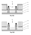
- Figure 1 shows a schematic (a) cross section (500) and (b) tilted view (501) of a patterned substrate.
- the patterned substrate (500, 501) comprises a semiconductor region (12) and a dielectric region (11).
- the dielectric region (11) comprises a dielectric material (20), which is typically SiO 2 , that is in contact with a semiconductor substrate (10).
- the semiconductor substrate (10) may be a Si or Ge substrate (10) such as a Si wafer or a Ge wafer.
- the semiconductor substrate may also be a silicon on insulator (SOI) or germanium on insulator (GeOI) substrate.
- the semiconductor region (12) may comprise a plurality of structures having lateral walls and a top surface that protrude from the dielectric material (20).
- the plurality of structures are fin structures (40).
- the patterned substrate as illustrated in Fig. 1 (a) and Fig. 1 (b) may form the basis for forming a finFET device comprising the plurality of fin structures (40).
- the patterned substrate (500, 501)) may be manufactured by using the Shallow Trench Isolation (STI) approach as known in semiconductor manufacturing.
- the dielectric material (20), which is SiO 2 functions as isolation material. Either STI-last or STI-first approach may be used as known in the art to produce the patterned substrate (500, 501) such as that shown in Fig. 1 (a) or Fig. 1(b) .
- the fin structures (40) may comprise a Group III-V compound semiconductor.
- the fin structures (40) may also comprise at least one element selected from the group consisting of Si and Ge.
- the fin structures (40) may be doped with a dopant element at a desired doping concentration defined by the technology node in question. Doping of the fin structures leads to the formation of an n-type or p-type channel depending on the type of the dopant element.
- the height and width of the fin structures may be defined by the choice of the technology node in question.
- a top surface of the semiconductor region and a top surface of the dielectric region may be abutting on a same surface, such as for example in a planar FET device.
- the fin structures (40) may comprise a gate stack (43) covering a channel region, and spacers (not shown in the figure), which embed the gate stack on both sides.
- the channel region is located in between a source region (41) and a drain region (42) as shown in Fig. 1(c) .
- the gate stack (43) may be a dummy gate stack comprising, for example, a thin layer of SiO 2 as the dummy gate dielectric (not shown in the figures)and amorphous silicon (a-Si) as the dummy gate metal.
- the fin structures (40) in the source region (41) and the drain region (42) may be recessed followed by epitaxial regrowth.
- the epitaxially regrown source and drain in this fashion are typically referred to as embedded source and drain and may be formed from the same semiconductor material as that of the fin structures, such for example a Ge fin and epitaxially regrown Ge on it.
- the epitaxially regrown source and drain may also be formed from a different semiconductor material, such for example a Ge fin and epitaxially regrown SixGe 1-X on it. Epitaxial regrowth of the source/drain proceeds until the original height of the fin structures (40) is reached.
- regrowth is done typically up to the original fin height.
- the shape of the epitaxial regrown part might differ due to different growth rate along different crystallographic planes.
- SiGe typically grows diamond shaped between gates, while the shape is more of a triangular shape for Si. In-situ doping during epitaxial regrowth or doping after epitaxial regrowth by ion implantation may be performed.
- the doping may be done by using a suitable dopant element such as for example by using a p-type or an n-type dopant such that it results in a highly-doped source/drain so as to minimize contact resistance.
- a suitable dopant element such as for example by using a p-type or an n-type dopant such that it results in a highly-doped source/drain so as to minimize contact resistance.
- Contact resistance is already a key contributor to device performance at state-of-the art N14 technology in semiconductor industry. Lowering the contact resistivity and increasing the contact area allows for reducing the contact resistance.
- Typical doping concentration targeted for source/drain in technology nodes smaller than N10 in semiconductor manufacturing is at least 1x10 20 /cm 3 .
- a contact resistance value of sub 1e-9 Ohm.cm2 is targeted for N7 and N5 technology. This can probably only be achieved with dopant concentrations exceeding 1e21 at/cm 3 .
- epitaxial regrowth may take place directly on the fin structures (40).
- the epitaxially regrown source and drain in this fashion are typically referred to as raised source and drain.
- In-situ doping or doping after regrowth may be performed in the same way as that of embedded source and drain formation module.
- the shape of the epitaxially regrown source drain regions depends on whether the epitaxial regrowth can take place freely or whether the regrowth is confined by a kind of spacer material in which case the epitaxial regrowth will only fill up the cavity created by fin recess.
- the dummy gate stack (43) is replaced with the actual gate stack that comprises a high-k dielectric material, as the gate dielectric, and a gate metal.
- This is called high-k last replacement metal gate module (HKL-RMG) as known in the art.
- this HKL-RMG takes place before opening the contact holes, which reach to the source and drain region through an interlayer dielectric.
- the method according to the embodiments of the present invention enables carrying out the HKL-RMG after contact hole opening and electrical contact formation therein.
- alignment markers may be damaged. Alignment markers are used when consecutive lithography and etching processes are to be performed for patterning layers so that layers can be aligned in the intended way with respect to each other to end up with correct patterning. Damage to the alignment markers can further cause alignment problems for contact hole opening. It is thus, an advantage of the embodiments of the present invention that postponing the replacement until after contact hole opening and contact formation allows performing the correct alignment with respect to the a-Si dummy gate metal.
- Figure 2 (a) to Figure 2(h) show schematically fabricating a semiconductor structure according to embodiments of the present invention.
- a conformal layer of a first dielectric material (30) may be deposited directly on the patterned substrate (500, 501), thereby covering the semiconductor region (12) and the dielectric region (11).
- the first dielectric material (30) may be a metal oxide, a silicon oxide or a silicon nitride.
- the silicon nitride may be Si 3 N 4 .
- the metal oxide may be an aluminum oxide or titanium oxide.
- the aluminum oxide may be Al 2 O 3 .
- the titanium oxide may be TiO 2 .
- the first dielectric material may be the silicon oxide.
- the silicon oxide may be SiO 2 .
- the first dielectric material (30) may be deposited by using Atomic Layer Deposition (ALD), Chemical Vapor Deposition (CVD) or Low-Pressure Chemical Vapor Deposition (LP-CVD).
- ALD Atomic Layer Deposition
- CVD Chemical Vapor Deposition
- LP-CVD Low-Pressure Chemical Vapor Deposition
- the first dielectric material (30) may, therefore, be deposited by using ALD process, since it allows for depositing a conformal and thin layer on the patterned substrate (500, 501).
- the thickness of the first dielectric material may be in the range of 1 nm to 5 nm.
- a layer of a sacrificial material (60) is deposited directly on the first dielectric material (30) ( Fig. 2(b) ) .
- the sacrificial material covers the surface of the patterned substrate and embeds the fin structures(40) on all sides.
- the sacrificial material (60) may be deposited by Plasma Enhanced Chemical Vapor Deposition (PE-CVD).
- PE-CVD Plasma Enhanced Chemical Vapor Deposition
- the sacrificial material (60) may be an amorphous carbon material or an amorphous silicon material.
- Both the amorphous carbon material and the amorphous silicon material are suitable to be used as the sacrificial material owing to the fact that they have good etch selectivity with respect to SiO 2 or Si 3 N 4 , which may be chosen as the conformal layer of the first dielectric material.
- Patterning the sacrificial material (60) comprises providing a patterned photoresist layer (75) on the sacrificial material (60) ( Fig. 2(c) ). The sacrificial material (60) is then dry plasma etched using the patterned photoresist layer (75) as a mask. After dry plasma etching is completed, patterned photoresist layer (75) is removed ( Fig. 2(d) ) . Patterning of the sacrificial material (60) is done such that at least a part of the semiconductor region remains covered by the patterned sacrificial material (65). Besides, dry plasma etching of the sacrificial material (60) is selective to the conformal layer of the first dielectric material (30).
- This selective dry plasma etching process provides an advantage that the conformal layer of the first dielectric material (30) still remains on the patterned substrate after patterning of the sacrificial material (60) is completed.
- An electrical contact (100) is further to be formed on this part of the semiconductor region. More specifically, patterning of the sacrificial material (60) is done such that a pattern (65) of the patterned sacrificial material that is formed corresponds to or overlaps with an area of the patterned substrate that comprises a part of the semiconductor region on which an electrical contact (100) is to be formed.
- Providing a patterned photoresist layer (75) comprises depositing a photoresist layer (70) on the sacrificial material (60) ( Fig. 2(b) ) , followed by exposure of the photoresist layer by performing a lithographic patterning process.
- the lithographic patterning process may be deep ultra violet (DUV), extreme ultra violet (EUV),or 193 nm immersion lithography.
- a layer of a second dielectric material (80) is deposited on the patterned substrate ( Fig. 2 (e) ).
- the second dielectric material (80) completely embeds the patterned sacrificial material (65) from lateral sides and from the top surface.
- the second dielectric material (80) may for instance be deposited by self-aligned chemical vapor deposition (SA-CVD), high density plasma chemical vapor deposition (HDP-CVD), flowable deposition or plasma enhanced atomic layer deposition (PE-ALD).
- the second dielectric material (80) may be a silicon oxide.
- the silicon oxide may be SiO 2 .
- the second dielectric material (80) is typically referred to as interlayer dielectric zero (ILD0).
- the sacrificial material (60) may be an amorphous silicon material. It is advantageous to use amorphous silicon as the sacrificial material (60) due to the fact that a high temperature treatment, such as above 600 °C, is preferably used in order to densify the second dielectric material (80) after deposition. If Ge or SiGe is used as the channel material for p-MOS, a lower densification temperature of 550 °C or below down to room temperature is preferably used.
- Amorphous silicon is quite stable at high temperatures, such as above 600 °C, for densification of the second dielectric material (80), which is SiO 2 .
- the second dielectric material which is SiO 2 .
- the amorphous carbon is preferably used when the second dielectric material is densified at a temperature of 550°C or below.
- the amorphous carbon material may be an advanced patterning film (APF).
- the APF layer may be deposited at a temperature in the range of 400 °C to 550 °C.
- patterning of the sacrificial material comprises providing a patterned photoresist layer (75) on the sacrificial material (60) ( Fig. 2(c) ).
- the sacrificial material (60) is then dry plasma etched using the patterned photoresist layer (75) as a mask. After dry plasma etching is completed, patterned photoresist layer (75) is removed.
- patterning of the sacrificial material (60) may comprise providing a hard mask layer (not shown in the figures) sandwiched and in contact with the sacrificial material (60) and the photoresist layer (70).
- Resist masks are typically soft, thin and they shrink when subjected to an etch plasma, thus making them unreliable as a masking layer when dimensions are scaling. Therefore, it is advantageous to use the hard mask as described.
- the hard mask layer is etched by performing a dry plasma etching process.
- the patterned photoresist layer is removed, thereby leaving a patterned hard mask layer on the sacrificial material (60).
- the patterned hard mask layer is further used as a mask for dry plasma etching of the sacrificial material (60). Following the completion of dry plasma etching, the patterned hard mask layer is removed.
- the hard mask layer may be a silicon oxide or a silicon nitride.
- the silicon oxide may be SiO 2 .
- the silicon nitride may be Si 3 N 4 .
- the inventors have found out that depositing the conformal layer of the first dielectric material (30) directly on the patterned substrate (500, 501) according to embodiments of the present invention is advantageous. This is due to the fact that some of the deposition techniques used to deposit the layer of the second dielectric material, which is SiO 2 , involve a step where the substrate is subjected to an ozone atmosphere so as to initiate the deposition of SiO 2 .
- a self-aligned chemical vapor deposition process or a flowable oxide deposition process involves ozone in the onset of deposition.
- This step involving ozone exposure may damage the semiconductor region, more specifically the fin structures (40), especially when the semiconductor region is made of Ge or is Ge-comprising. The damage is created due to the oxidation of the Ge or Ge comprising semiconductor region, which then becomes prone to removal in aqueous environment.
- presence of the conformal first dielectric material covering the surface of the semiconductor structure avoids these damages to occur.
- a chemical mechanical planarization (CMP) process may be performed until a top surface (66) of the patterned sacrificial material (65) is revealed Fig. 2 (f) .
- the patterned sacrificial material (65) is removed completely selectively to the conformal layer of the first dielectric material (30), thereby forming a recess (90) ( Fig. 2(g) ).
- the recess (90) may be referred to as a contact hole.
- the recess (90) exposes at its bottom the conformal layer of the first dielectric material (30) and the recess has lateral walls comprising the second dielectric material (80). Removal of the patterned sacrificial material (65) may be done by performing a dry etch plasma process.
- Complete removal of the patterned sacrificial material (65) selectively to the conformal layer of the first dielectric material (30) has the advantage that the semiconductor region masked by the patterned sacrificial material (65) is not exposed to the chemistry used during the removal and therefore is still protected.
- removal may be done by subjecting the patterned substrate to a dry etch plasma comprising O 2 /N 2 H 2 .
- amorphous silicon may be used as the sacrificial material (60)
- removal of the patterned sacrificial material may be done by subjecting the semiconductor structure to a dry etch plasma comprising HBr/Cl 2 .
- amorphous silicon may be easily removed by a wet etching process, whereby tetra methyl ammonium hydroxide (TMAH) is used as the wet etch process liquid.
- TMAH tetra methyl ammonium hydroxide
- the exposed layer of the first dielectric material (30) at the bottom of the recess (90) is removed selectively to the semiconductor region ( Fig. 2(h) ). As a result of this removal, at least a part of the semiconductor region (12) is exposed.
- the exposed part of the semiconductor region may be a part of a source region (41) or a drain region (42) of a field effect transistor (FET).
- FET field effect transistor
- the field effect transistor may be a fin-type field effect transistor (finFET).
- the finFET comprises structures having lateral walls and a top surface that protrude from the dielectric material (20) of the dielectric region (11) and these protruding structures are fin structures (40).
- the source region or drain region are comprised in the fin structures.
- a part of the dielectric region (11) may also be exposed (11').
- the exposed part of the fin structures (40) may protrude from the dielectric material (20) of the exposed part (11') of the dielectric region (11).
- removing the first dielectric material (30) selectively to the semiconductor region (12) may be done by performing a wet etching process.
- removing the first dielectric material (30) selectively to the semiconductor region (12) may be done by performing a vapor treatment process, whereby the semiconductor structure is subjected to a vapor.
- the aluminum oxide or the titanium oxide can both be removed selectively to the semiconductor region by a wet etching process, whereby an ammonia-peroxide liquid mixture (APM) is used as the wet etch process liquid.
- APM ammonia-peroxide liquid mixture
- the silicon nitride can be removed by a wet etching process, whereby hot phosphoric acid (H 3 PO 4 ) may be used as the wet etch process liquid.
- hot (H 3 PO 4 ) should be done in caution since it is a strong etchant and may thus cause damages on the substrate and lead to issues in terms of defectivity.
- the thin Si 3 N 4 layer may first be oxidized by methods known to persons skilled in the art. Subsequently, removal may be achieved by using a aqueous HF solution. Typically, a concentration of less than 1 volume % is used in order to provide low and controllable etch rate. However, this may cause damages on the substrate as well such as for example irregular etching, such as for example anisotropic etching.
- the silicon oxide can be removed by a wet etching process, whereby a aqueous hydrogen fluoride (HF) is used as the wet etch process liquid. Furthermore, the silicon oxide can also be removed by performing a vapor HF treatment.
- a aqueous hydrogen fluoride (HF) is used as the wet etch process liquid.
- the silicon oxide can also be removed by performing a vapor HF treatment.
- the first dielectric material (30) may be SiO 2 , since it can be easily removed by a wet etching process, whereby an aqueous HF solution is used as the wet etch process liquid. Typically, a concentration of less than 1 % volume is used in order to provide low and controllable etch rate.
- silicon oxide is further advantageous to be used as the first dielectric material owing to the fact that it is easily deposited on the semiconductor structure.
- the advantage of selective wet etching process done in order to remove the first dielectric material is such that the exposed part of the semiconductor region is undamaged.
- the dopant concentration within the exposed part of the semiconductor region is kept substantially at the intended level that was achieved by doping during and/or after the source/drain formation module. This results in a finFET device with minimized contact resistance.
- Figure 3 shows a cross section (a) TEM image and (b) schematic representation of a cross-section of the exposed part of the semiconductor region of a semiconductor structure that is damaged after a contact opening process is done to form the contact hole (90) according to the prior art.
- the typical contact opening process comprises depositing the second dielectric material (80) on the patterned substrate (500, 501).
- a patterned photoresist layer (75) is provided on the second dielectric material (80) comprising patterned photoresist features and apertures in between these patterned photoresist features (75).
- a contact hole (90) is formed by dry plasma etching through the second dielectric material (80) using the patterned photoresist layer as a mask.
- patterned photoresist features are not provided on the second dielectric material (80) in order to form the recess (90) in the second dielectric material (80) by etching through the second dielectric material (80) using the patterned photoresist features as a mask. Since usage of patterned photoresist features are avoided on the second dielectric material (80), performing the strip process after formation of the contact hole (90) becomes obsolete. Absence of the strip process after formation of the contact hole (90), in embodiments of the present invention, is advantageous due to the fact that the strip process chemistry may potentially oxidize the exposed part of the semiconductor region. The oxidized layer is susceptible to removal. Removal may then result in material loss from the exposed part of the semiconductor region and thus leading to a change in the dopant concentration from the intended level that was achieved during and/or after the source/drain formation module by doping.
- the semiconductor structure (600) comprises a patterned substrate (500, 501) that comprises a semiconductor region and a dielectric region.
- a layer of a second dielectric material (80) overlays the patterned substrate.
- the second dielectric material (80) has a recess (90) that exposes a part of the semiconductor structure (600).
- the exposed part (1) of the semiconductor structure (600) comprises at least a part of the semiconductor region.
- the exposed part of the semiconductor region may be a part of a source region or a drain region of a field effect transistor (FET).
- FET field effect transistor
- the field effect transistor is a fin-type field effect transistor (finFET).
- the finFET comprises structures having lateral walls and a top surface that protrude from the dielectric material (20) and these protruding structures are fin structures (40).
- the semiconductor structure (600) further comprises a conformal layer of a first dielectric material (30) present on an un-exposed part (2) of the semiconductor structure.
- FIG. 5 (a) Fig. 5(e) showing schematically the formation of an electrical contact to a semiconductor structure according to embodiments of the present invention.
- a semiconductor structure (600) such as that represented schematically in Fig. 4 is provided.
- the semiconductor structure (600) may be fabricated according to embodiments of the present invention.
- the semiconductor structure (600) comprises a patterned substrate (500, 501) that comprises a semiconductor region and a dielectric region.
- a layer of a second dielectric material (80) overlays the patterned substrate.
- the second dielectric material (80) has a recess (90) that exposes, at its bottom, a part (1) of the patterned substrate.
- the exposed part (1) of the semiconductor structure (600) comprises at least a part of the semiconductor region.
- the exposed part (1) of the semiconductor structure (600) may further comprise an exposed part (11') of the dielectric region (11).
- the exposed part (1) of the semiconductor region may be a part of a source region or a drain region of a field effect transistor (FET).
- FET field effect transistor
- the field effect transistor is a fin-type field effect transistor (finFET).
- the finFET comprises structures having lateral walls and a top surface that protrude from the dielectric material (20) of the dielectric region (11) and these protruding structures are fin structures (40).
- the source region or drain region are comprised in the fin structures.
- the exposed part (1) of the semiconductor structure (600) may comprise the exposed part (11') of the dielectric region (11), and the exposed part of the fin structures (40), where the exposed part of the fin structures (40) protrude from the exposed part (11') of the dielectric region (11).
- the semiconductor structure (600) further comprises a conformal layer of a first dielectric material (30) present on an un-exposed part (2) of the patterned substrate.
- the un-exposed part (2) of the semiconductor structure (600) may comprise an un-exposed part of the source region or drain region of a first fin structure that extend longitudinally along a direction from the exposed part of the (same) source region or (same) drain region comprised in the exposed part of the patterned substrate.
- the un-exposed part (2) of the semiconductor structure (600) may comprise an un-exposed part of the source region or drain region of a second fin structure that is displaced along a direction horizontally away from the first fin structure.
- the profile of the exposed part of the source region or the drain region of the first fin structure may substantially be the same as that of the un-exposed part of the source region or the drain region of the first or of the second fin structure.
- a self-assembled monolayer (95) material may be selectively applied on the semiconductor structure (600).
- the self-assembled monolayer (95) covers conformally the semiconductor structure (600), whereby the exposed part of the semiconductor region remains uncovered ( Fig. 5 (b) ).
- Selective application of the SAM material on the second dielectric material (80) and/or the exposed part of the dielectric region (11') of the semiconductor structure (600) implies choosing a suitable SAM material such that its head group has affinity to bind to the exposed surfaces of the second dielectric material (80) and/or the dielectric region. Therefore, in embodiments of the present invention, the SAM material may be chosen such that its head group has affinity to bind to SiO 2 .
- Such a SAM material may be chosen from a group consisting of silanes which are typically selectively grafted to the Si-OH groups on the silicon oxide, or silicon nitride surface.
- silanes which are typically selectively grafted to the Si-OH groups on the silicon oxide, or silicon nitride surface.
- -CH3 hydrophobic, non-reactive groups and long alkyl chain length of the silanes such C10-C18, and preferably C18
- a dense film may be formed which will inhibit ALD nucleation making the ALD deposition of the metal to be selective on the exposed part of the semiconductor region.
- the alkyl trichloro or trialkoxy (Methoxy or ethoxy) silanes C10 to C18
- organic solvents namely alcohols (i.e. ethanol, butanol, ipa propanol..) or toluene in mili molar (mM) precursor concentration as known to persons skilled in the art.
- the exposed semiconductor region should be cleaned such that the surface of the exposed semiconductor region becomes oxide free.
- the oxide which is usually a native oxide as referred by persons skilled in the art, should preferably be cleaned from the surface of the exposed semiconductor region prior to SAM material deposition.
- this surface cleaning resulting in oxide removal may be done by a dry oxide removal process subsequently followed by in-situ vapor SAM deposition in the same process tool without air break.
- this surface cleaning resulting in oxide removal may be done by a wet oxide removal process subsequently followed by in-situ liquid SAM deposition in the same process tool without air break.
- This in-situ SAM material deposition done either by depositing the SAM material from vapor phase or liquid phase has the advantage that the cleaned surface of the semiconductor region is not exposed to air, thus avoiding re-oxidation of the surface.
- the SAM material which is deposited selectively on the second dielectric material (80) and/or exposed part (11') of the dielectric region (11) of the semiconductor structure (600), is attached to the silicon oxide or silicon nitride through chemisorption.
- SAM material may be deposited on the exposed part of the semiconductor region through physisorption. This physisorbed SAM layer should be removed from the exposed part of the semiconductor region before depositing the metal by ALD.
- a thermal annealing at a temperature lower than 400 °C may be done to remove physisorbed SAM material layer from the exposed part of the semiconductor region.
- the thermal annealing may be done at a temperature in the range of 200 °C to 400 °C. It is advantageous that the temperature is chosen in the range of 200 °C to 400 °C so that only the SAM material that is attached to the exposed semiconductor region through physisorption is removed. Thermal annealing done at a temperature higher than 400 °C risks the removal of SAM material attached through chemisorption to the silicon oxide or silicon nitride, which is undesirable.
- extra rinsing of the semiconductor structure in organic solvents such as alcohol and/or acetone and/or water may be applied to remove physisorbed SAM material layer from the exposed part of the semiconductor region (1).
- This rinsing only removes the physisorbed SAM precursors, while leaving the chemisorbed SAM present on the second dielectric material (80) and/or the exposed part (11') of the dielectric region (11) of the semiconductor structure (600) unremoved.
- the extra rinsing and the thermal annealing may both be applied to remove the_physisorbed SAM material layer from the exposed part of the semiconductor region.
- An electrical contact (100) is formed, at the bottom of the recess (90), conformally on the exposed part of the semiconductor region ( Fig. 5 (c) ).
- This exposed part of the semiconductor region is the region that remains uncovered after the SAM is selectively applied on the semiconductor structure.
- an electrical contact is formed conformally on the exposed part of the semiconductor region, which is a part of a source region or a drain region of a FET, where the FET is, preferably, a finFET.
- the FET is, preferably, a finFET.
- source region or drain region when the source region or drain region is epitaxially grown during the contact formation module, source region or drain region may be diamond shaped. Therefore, it is advantageous to form the conformal electrical contact to a depth that allows to contact the entire source region and drain region, which is highly doped. Contacting the entire source region or drain region refers to the fact that the conformal electrical contact is formed not only at the top but also laterally on the side of the source region or drain region according to embodiments of the present invention. Such kind of an electrical contact is referred to as a wrap-around contact. Contacting the highly doped source region or drain region from all sides has the advantage of enabling contact resistance minimization since the contact area is maximized.
- formation of the electrical contact (100) comprises depositing selectively a metal on the exposed part of the semiconductor region in the bottom of the recess (90) (not shown in the figures.
- a vapor-solid reaction is performed, whereby the semiconductor structure (600) is subjected to a silicon-comprising precursor gas or a germanium-comprising precursor gas.
- Subjecting the semiconductor structure to the silicon-comprising precursor gas or to the germanium-comprising precursor gas converts the metal to a metal silicide or a metal germanide.
- Performing a vapor-solid reaction is advantageous since it allows formation of the electrical contact without consuming the substrate.
- the Si-comprising precursor gas or Ge-comprising precursor gas reacts with the metal and the electrical contact is formed by conversion of the metal into the metal-silicide or the metal germanide, thus keeping the exposed part of the semiconductor region intact. Since the exposed part of the semiconductor region is kept intact and not consumed during the formation of the electrical contact, the dopant concentration in this region is not reduced, thus it remains unchanged. Reduction of the dopant concentration during electrical contact formation that may occur if the metal reacts with the exposed part of the semiconductor region leading to increase in contact resistance, is undesirable.
- the metal may be nickel.
- Nickel is typically used for forming electrical contacts to semiconductor structures thanks to its ability to form low resistance electrical contacts.
- the selective deposition of the metal may be done in a first deposition tool up to a desired thickness by performing a physical vapor deposition (PVD), sputtering deposition, chemical vapor deposition (CVD) or an atomic layer deposition process (ALD). Attention is paid to the fact that the deposition temperature of the metal should be kept lower than 400 °C due to the fact that otherwise the SAM material attached to silicon oxide or silicon nitride through chemisorption risks to be partially or completely removed.
- PVD physical vapor deposition
- CVD chemical vapor deposition
- ALD atomic layer deposition process
- selective deposition of the metal may be done by performing an ALD process.
- the desired thickness of the metal may be in the range of 2 nm to 80 nm.
- the desired thickness of the metal may be in the range of 4 nm to 10 nm. It is advantageous to have the desired thickness of metal in this range due to the fact that for thicknesses higher than 10 nm, the risk exists such that the metal deposition may be non-selective; for instance it may also be deposited onto the SAM material.
- the vapor solid reaction may be carried out in a second deposition tool at a temperature in the range of 215 °C to 350 °C.
- the second deposition tool may be a chemical vapor deposition (CVD) tool.
- the vapor-solid reaction may be carried out at a temperature in the range of 215 °C to 250 °C.
- the germanium-comprising precursor gas may be used.
- the germanium-comprising precursor gas may comprise one or more compounds selected from the list consisting of GeH 4 , Ge 2 H 6 , trigermane, isobutylgermane, tetramethylgermane and halides of germanium, such as for example GeCl 4 , GeF 2 or GeBr 2 .
- the temperature may be 225 °C and GeH 4 may be used as the Ge-comprising precursor gas. It is an advantage to use GeH 4 since it is the simplest Ge-comprising precursor gas.
- the electrical contact formed is a Ge-comprising alloy.
- the Ge comprising alloy may be a mono-nickel-germanide (NiGe).
- the Ge-comprising precursor gas may be diluted with H 2 .
- the diluted Ge-comprising precursor gas may be provided into the second deposition chamber in the presence of a carrier gas.
- the carrier gas may be an inert gas.
- Ar, He or N 2 may be used as carrier gas.
- the purpose of using carrier gas is to regulate the partial pressure of Ge-comprising precursor gas.
- the carrier gas is, preferably, N 2 .
- the flow rate of Ge-comprising precursor gas may be in the range of 100 sccm to 4000 sccm.
- Pressure of the second deposition tool may be in the range of 1.0 Torr to 6.0 Torr.
- Exposure time to Ge-comprising precursor gas may be in the range of 15 seconds to 300 seconds.
- the vapor-solid reaction may be carried out at a temperature in the range of 225 °C to 350 °C.
- the silicon-comprising precursor gas may be used.
- the silicon comprising precursor gas may be halides of Si (SiCl 4 , SiBr 4 , SiCl 2 H 2 ), tetraethyl orthosilicate (TEOS), hexamethyldisiloxane (HMDSO), tetraethylsilane, pentamethylsilane, hexamethyldisilane, or tetramethylsilane, methylsilane.
- TEOS tetraethyl orthosilicate
- HMDSO hexamethyldisiloxane
- tetraethylsilane pentamethylsilane, hexamethyldisilane, or tetramethylsilane, methylsilane.
- the silicon-comprising precursor gas may be SiH 4 .
- the electrical contact formed is a Si comprising alloy.
- the Si comprising alloy may be a mono-nickel-silicide (NiSi).
- the Si-comprising precursor gas may be diluted with H 2 .
- the diluted Si-comprising precursor gas may be provided into the second deposition chamber in the presence of a carrier gas.
- the carrier gas may be an inert gas.
- Ar, He or N 2 may be used as carrier gas.
- the flow rate of Si-comprising precursor gas may be in the range of 100 sccm to 900 sccm.
- Pressure of the second deposition tool may be in the range of 1.0 Torr to 6.0 Torr.
- Exposure time to Si-comprising precursor gas may be in the range of 15 seconds to 300 seconds.
- formation of the electrical contact (100) may comprise selectively depositing a layer stack on the exposed part of the semiconductor region by using an ALD process (not shown in the figures).
- the layer stack may comprise a metal in contact with the exposed part (1) of the semiconductor region in the bottom of the recess (90) and a metal nitride layer on and in contact with the metal.
- the thickness of the metal may be in the range of 1 nm to 5 nm
- the thickness of the metal nitride may be in the range of 1 nm to 5 nm
- the metal may be Ti.
- Ti is advantageous since it is a good oxygen getter allowing to avoid residual oxide at the interface between semiconductor region and the metal itself. Presence of residual oxide can adversely influence the contact resistance. Furthermore, Ti advantageously covers the source region or drain region completely.
- the metal nitride may be TiN.
- TiN may be deposited by ALD or by physical vapor deposition (PVD). When deposited by ALD, TiN is stoichiometric. When deposited by PVD, Ti/N ratio can be tuned, however the layer is typically Ti-rich.
- the self-assembled monolayer (95) material is removed selectively from the semiconductor structure (600) ( ( Fig. 5 (d) ).
- Removing the SAM material (95) selectively may be done by annealing at a temperature higher than 400C, or by applying plasma and/or UV ozone treatments and/or dipping in wet etching/oxidizing chemistry such as tetramethyl ammonium hydroxide (TMAH), hydrogen fluoride (HF), piranha solution, which is a mixture of hydrogen sulfide and hydrogen peroxide (H2SO4/H2O2).
- TMAH tetramethyl ammonium hydroxide
- HF hydrogen fluoride
- piranha solution which is a mixture of hydrogen sulfide and hydrogen peroxide
- a contact metal (110) is provided on the semiconductor structure (600) filling in the recess (90).
- the contact metal may also be referred to as a contact metal fill in the art.
- the contact metal (110) is tungsten (W) and it is deposited by an ALD or a CVD process.
- the contact metal (110) may be a Ni-comprising contact metal fill or a Co-comprising contact metal fill.
- the Ni-comprising contact metal fill or the Co-comprising contact metal fill may be provided by performing an electroplating process.
- a CMP process is performed until a top surface of the second dielectric material (80) is revealed.
- the CMP process removes excess contact metal (110) overlaying the semiconductor structure (600), thereby resulting in a flat surface ( Fig. 5 (e) ).
Landscapes
- Chemical & Material Sciences (AREA)
- Chemical Kinetics & Catalysis (AREA)
- General Chemical & Material Sciences (AREA)
- Insulated Gate Type Field-Effect Transistor (AREA)
- Thin Film Transistor (AREA)
Abstract
Description
- The present invention is related to the formation of a field effect transistor device having an electrical contact. The main application is for fin-type field effect transistor devices.
- As the transistor sizes are reducing in pursuit of Moore's law, increase in series resistance towards the channel is becoming a challenge. This is due to the fact that the performance of the device, such as for example, sub-threshold slope (SS), drain induced barrier lowering (DIBL) and drain saturation current (IDsat) can adversely be influenced if the series resistance is not minimized. This has to do mainly with the increase in contact resistance, which is one of the main components of the series resistance.
- Contact resistance is a function of the resistance of (1)contact metal fill, (2)interface metal/semiconductor resistivity and (3)contact area.
- 1. Resistance of the fill metal is depending on whether the material needs to be integrated with contact liners and what the contribution of these contact liners is to the overall resistance.
- 2. Metal/semiconductor resistivity is a function of the number of active dopants at the interface and the choice of interface metal. In pursuit of Moore's Law, alternative material choices are introduced instead of silicon, such as strained silicon (s-Si), strained germanium (s-Ge) SiGe, or III-V compound semiconductor materials, to form the channel of a field effect transistor (FET)
- In this respect, the choice of interface metal may depend on the type of material in the source and drain (S/D) region of the FET, which is chosen among the aforementioned alternative materials to be integrated for nMOS and pMOS, respectively. Additionally, the formation and thermal stability of the electrical contact as a function of the choice of the interface metal also plays a role.
- Additionally, with the device scaling in pursuit of Moore's Law, introduction of new FET designs such as fin-type FET (finFET) or Tri-gate FET has taken place. Thus, there is a trend to integrate taller fin structures at tighter pitch to maximize drive current per footprint (accelerated by fin depopulation considerations). This leads to reduction in the contact area, which in turns leads to an increase in contact resistance. Besides, in relation with the influence of contact area, contact opening is also critical since the damage on the S/D region of the FET within the contact area is typically created during contact opening. Damage to the S/D region risks altering the number of active dopants, which in turn influences the aforementioned metal/semiconductor resistivity thus, resulting in an increase in contact resistance.
- There is, therefore, a need in the art for a method that can enable the formation of an electrical contact on or completely surrounding the source region and drain region of a FET without resulting in damage to the substrate in the source/drain region; thus leading to an electrical contact having minimized contact resistance.
- It is an object of the present invention to provide good methods for fabricating a semiconductor structure.
- It is an advantage of embodiments of the present invention that the method allows fabricating a semiconductor structure that has an undamaged source region or drain region.
- It is an advantage of embodiments of the present invention that the method allows producing a semiconductor structure suitable for fabricating FETs particularly requiring doping concentration of at least 1x10²⁰/cm3 in the source region or drain region.
- It is an advantage of embodiments of the present invention that the method allows forming an electrical contact with reduced contact resistance on source region or drain region thanks to the undamaged source region or drain region.
- It is an advantage of embodiments of the present invention that the method allows forming an electrical contact, which is conformal and contacts the entire source region or drain region such that the electrical contact is formed not only at the top but also laterally on the side of the source region or drain region.
- It is an advantage of embodiments of the present invention that the method allows carrying out the high-k last replacement metal gate (HKL-RMG) module after contact hole opening and electrical contact formation therein. This diminishes the problem of damaging the alignment markers. Damaging the alignment markers may typically occur when HKL-RMG is carried out before opening the contact hole and forming the electrical contact.
- The above objective is accomplished by a method according to the present invention.
- In a first aspect, the present invention relates to a method for fabricating a semiconductor structure. The method comprises providing a patterned substrate comprising a semiconductor region and a dielectric region. Directly on the patterned substrate a conformal layer of a first dielectric material is deposited. The deposited conformal layer of a first dielectric material, thereby covers the semiconductor region and the dielectric region. A layer of a sacrificial material is deposited on the conformal layer of the first dielectric material. The sacrificial material is patterned, whereby at least a part of the semiconductor region remains uncovered by the patterned sacrificial material. A layer of a second dielectric material is deposited on the patterned substrate that completely covers the patterned sacrificial material. An excess portion of the second dielectric material is removed by performing a surface flattening process, thereby exposing a top surface of the patterned sacrificial material. A recess is formed in the second dielectric material by completely removing the patterned sacrificial material selectively to the conformal layer. Complete removal of the patterned sacrificial material exposes the conformal layer of the first dielectric material at the bottom of the recess. The exposed conformal layer of the first dielectric material is removed selectively to the semiconductor region. This selective removal at least exposes the part of the semiconductor region.
- In embodiments, patterning the sacrificial material may comprise providing a patterned photoresist layer on the sacrificial material. The patterned photoresist layer may be defined by photoresist features separated by apertures, whereby the apertures expose the sacrificial material. The sacrificial material is dry plasma etched using the patterned photoresist layer as mask. After completion of the dry plasma etching, patterned photoresist layer is removed by performing a photoresist strip process.
- In embodiments, removing the exposed conformal layer of the first dielectric material selectively to the semiconductor region may be done by performing a wet etching process.
- In embodiments, removing the exposed conformal layer of the first dielectric material selectively to the semiconductor region may also be done by subjecting the semiconductor structure to a vapor treatment.
- In embodiments of the present invention, removal of the exposed conformal layer of the first dielectric material by performing the wet etching process or the vapor treatment is advantageous since it avoids creating damages on the semiconductor region from which it is removed.
- In embodiments, the sacrificial material may be an amorphous carbon material or an amorphous silicon material.
- It is an advantage according to embodiments of the present invention that the amorphous carbon material or the amorphous silicon material has good etch selectivity with respect to the first dielectric material.
- In embodiments, the depositing of the conformal layer of the first dielectric material may be done by Atomic Layer Deposition (ALD).
- It is an advantage according to embodiments of the present invention that ALD provides a conformal layer of the first dielectric material on the patterned substrate. Furthermore, thickness of the first dielectric material deposited by ALD may be in the range of 1 nm to 10 nm, preferably in the range of 1 nm to 5 nm.
- In embodiments, the exposed part of the semiconductor region may be a part of a source region or of a drain region of a field effect transistor (FET).
- In embodiments, the present invention relates to a method for forming an electrical contact to a semiconductor structure. The method comprises providing a semiconductor structure fabricated according to any embodiments of the present invention.
- In embodiments, the semiconductor structure may comprise a patterned substrate. The patterned substrate may comprise a semiconductor region and a dielectric region. A layer of a second dielectric material may be overlaying on the patterned substrate. The second dielectric material has a recess that exposes a part of the semiconductor structure.
- In embodiments, the exposed part of the semiconductor structure may be a part of the semiconductor region.
- In embodiments, the exposed part of the semiconductor region may be a part of a source region or a drain region of a field effect transistor (FET).
- In embodiments, the field effect transistor may be a fin-type field effect transistor (finFET). The finFET may comprise structures having lateral walls and a top surface that protrude from the dielectric material. These protruding structures are fin structures.
- In embodiments, the semiconductor structure may further comprise a conformal layer of a first dielectric material present on an un-exposed part of the semiconductor structure. The un-exposed part of the semiconductor structure is overlaid by the second dielectric material.
- A self-assembled monolayer (SAM) material may be selectively applied on the second dielectric material and on an exposed part of the dielectric region of the semiconductor structure, whereby the exposed part of the semiconductor region remains uncovered. The electrical contact is formed on the exposed part of the semiconductor region at the bottom of the recess. Preferably, the electrical contact may be a conformal electrical contact. SAM material is selectively removed from the semiconductor structure.
- It is an advantage of embodiments of the present invention that selective application of the SAM material allows the formation of the electrical contact selectively on the exposed semiconductor region, which is not covered by the SAM material. This is advantageous since it removes the need for carrying out an additional chemical mechanical planarization step, which would otherwise be required to remove the metal from the field areas that are outside the recess.
- In embodiments, forming the electrical contact may further comprise depositing a contact metal overlaying the semiconductor structure filling in the recess. The contact metal is a contact metal fill.
- In embodiments, forming the electrical contact may comprise depositing selectively a metal on the exposed part of the semiconductor region at the bottom of the recess. A vapor-solid reaction is performed, whereby the semiconductor structure is subjected to a silicon-comprising precursor gas or a germanium comprising precursor gas thereby converting the metal to respectively a metal silicide or a metal germanide.
- It is an advantage according to embodiments of the present invention that the formation of the electrical contact does not depend on the materials choice of the exposed semiconductor region, on which the metal is deposited.
- It is also an advantage according to embodiments of the present invention that it allows the formation of the electrical contact without consuming the material of the exposed semiconductor region thanks to the vapor-solid reaction.
- In embodiments, forming the electrical contact may also comprise depositing a layer stack by using an ALD process. The layer stack may comprise a metal layer in contact with the exposed part of the semiconductor region at the bottom of the recess and a metal nitride layer on and in contact with the metal layer.
- In embodiments, the metal may be titanium (Ti). Ti is advantageous due to the fact that it is a good oxygen getter.
- In embodiments, the metal nitride may be titanium nitride (TiN). TiN is advantageous due to the fact that it forms a good interface between Ti and the contact metal.
- In embodiments, the electrical contact may be a wrap-around contact.
- It is an advantage according to embodiments of the present invention that the wrap-around contact allows for contacting the exposed semiconductor region from all sides. Contacting the exposed semiconductor region from all sides maximizes the contact area, thereby minimizing contact resistance.
-
-
Fig. 1 is a schematic (a) cross section and, (b) and (c) tilted view of a patterned substrate comprising on a main surface a semiconductor region and a dielectric region. -
Fig. 2 (a) toFig. 2(h) show schematically fabricating a semiconductor structure according to embodiments of the present invention. -
Fig. 3 is a cross section Transmission Electron Microscopy (TEM) image and (b) schematic representation of a semiconductor structure after formation of the recess. -
Fig. 4 shows a tilted view of a semiconductor structure fabricated according to embodiments of the present invention. -
Fig. 5 (a) toFig. 5(e) show schematically the formation of an electrical contact to a semiconductor structure according to embodiments of the present invention. - The present invention will be described with respect to particular embodiments and with reference to certain drawings but the invention is not limited thereto but only by the claims. The drawings described are only schematic and are non-limiting. In the drawings, the size of some of the elements may be exaggerated and not drawn on scale for illustrative purposes. The dimensions and the relative dimensions do not correspond to actual reductions to practice of the invention.
- It is to be noticed that the term "comprising", used in the claims, should not be interpreted as being restricted to the means listed thereafter; it does not exclude other elements or steps. It is thus to be interpreted as specifying the presence of the stated features, integers, steps or components as referred to, but does not preclude the presence or addition of one or more other features, integers, steps or components, or groups thereof.
- Reference throughout the specification to "one embodiment" or "an embodiment" means that a particular feature, structure or characteristic described in connection with the embodiment is included in at least one embodiment of the present invention. Thus, appearances of the phrases "in one embodiment" or "in an embodiment" in various places throughout the specification are not necessarily all referring to the same embodiment, but may. Furthermore, the particular features, structures or characteristics may be combined in any suitable manner, as would be apparent to one of ordinary skill in the art from the disclosure, in one or more embodiments.
- Similarly it should be appreciated that in the description of exemplary embodiments of the invention, various features of the invention are sometimes grouped together in a single embodiment, figure, or description thereof for the purpose of streamlining the disclosure and aiding in the understanding of one or more of the various inventive aspects. The method of disclosure, however, is not to be interpreted as reflecting an intention that the claimed invention requires more features than are expressly recited in each claim. Rather, as the following claims reflect, inventive aspects lie in less than all features of a single foregoing disclosed embodiment. Thus, the claims following the detailed description are hereby expressly incorporated into the detailed description, with each claim standing on its own as a separate embodiment of the invention.
- Furthermore, while some embodiments described herein include some but not other features included in other embodiments, combinations of features of different embodiments are meant to be within the scope of the invention, and form different embodiments, as would be understood by those in the art. For example, in the following claims, any of the claimed embodiments can be used in any combination.
- In the description provided herein, numerous specific details are set forth. However, it is understood that embodiments of the invention may be practiced without these specific details. In other instances, well-known methods, structures and techniques have not been shown in detail in order not to obscure an understanding of the description.
- The following terms are provided solely to aid in the understanding of the invention.
- As used herein and unless provided otherwise, the term "self-assembled monolayer (SAM) material" refers to molecular assemblies that form on the surfaces spontaneously by adsorption and are organized into more or less large ordered domains. SAM materials may possess a head group with a strong affinity to the substrate, a tail group and a functional end group. SAM materials are created by the chemisorption of the head groups onto the substrate from vapor or liquid phase followed by slow organization of the tail groups.
- As used herein and unless provided otherwise, the term "electrical contact" refers to a contact made on an area of a conducting or a semiconducting material.
- As used herein and unless provided otherwise, the term "technology node" refers to devices in semiconductor processing having a gate length at the indicated number such for example N10 refers to technology node having a gate length of 10 nm.
- As used herein and unless provided otherwise, the term "STI-last" refers to planar deposition of a material on a substrate followed by patterning it to make the fin structures and filling in the space between the fin structures with a dielectric material.
- As used herein and unless provided otherwise, the term "STI-first" refers to the growth of fin structures in trenches made in a dielectric material, which is provided on a substrate.
- As used herein and unless provided otherwise, the term "contact resistance" refers to the contribution to the series resistance of a field effect transistor, which depends on the resistivity of the metal/semiconductor resistivity and the area through which the metal contacts the semiconductor.
- As used herein and unless provided otherwise, the term "contact hole" refers to a recess made in a dielectric material overlying a patterned substrate. Contact hole exposes a part of a source region or a drain region of a FET and is filled with a contact metal fill to contact the source region or the drain region to an interconnect structure.
- As used herein and unless provided otherwise, the term "having a material that has good etch selectivity with respect to another material" refers to the etch rate of the material being higher than that of the another material given under prescribed etching conditions.
- As used herein and unless provided otherwise, the term "conformal" refers to being able to follow the topography of any surface.
- As used herein and unless provided otherwise, the term "exposed" refers to a layer, a surface or a region that is in contact with surrounding atmosphere.
- As used herein and unless provided otherwise, the term "un-exposed" refers to a layer, a surface or a region that is not in contact with the surrounding atmosphere.
- As used herein and unless provided otherwise, the term "etching a material selectively to another material" implies that the material is etched without etching the another material.
- As used herein and unless provided otherwise, the term "oxygen getter" refers to a material that scavenges oxygen.
- As used herein and unless provided otherwise, the term "wrap-around contact" refers to an electrical contact covering a source and/or a drain region from all exposed sides. When the field effect transistor device is fin-type field effect transistor (Fin-FET), wrap around contact refers to an electrical contact covering the top and part of the sidewalls of the fin structure, which define the source and/or drain region.
- We now refer to
Figure 1 . -
Figure 1 shows a schematic (a) cross section (500) and (b) tilted view (501) of a patterned substrate. The patterned substrate (500, 501) comprises a semiconductor region (12) and a dielectric region (11). - The dielectric region (11) comprises a dielectric material (20), which is typically SiO2, that is in contact with a semiconductor substrate (10). The semiconductor substrate (10) may be a Si or Ge substrate (10) such as a Si wafer or a Ge wafer. The semiconductor substrate may also be a silicon on insulator (SOI) or germanium on insulator (GeOI) substrate.
- The semiconductor region (12) may comprise a plurality of structures having lateral walls and a top surface that protrude from the dielectric material (20). The plurality of structures are fin structures (40). As it may be understood by a person skilled in the art, the patterned substrate as illustrated in
Fig. 1 (a) and Fig. 1 (b) may form the basis for forming a finFET device comprising the plurality of fin structures (40). - The patterned substrate (500, 501)) may be manufactured by using the Shallow Trench Isolation (STI) approach as known in semiconductor manufacturing. The dielectric material (20), which is SiO2, functions as isolation material. Either STI-last or STI-first approach may be used as known in the art to produce the patterned substrate (500, 501) such as that shown in
Fig. 1 (a) or Fig. 1(b) . The fin structures (40) may comprise a Group III-V compound semiconductor. The fin structures (40) may also comprise at least one element selected from the group consisting of Si and Ge. - The fin structures (40) may be doped with a dopant element at a desired doping concentration defined by the technology node in question. Doping of the fin structures leads to the formation of an n-type or p-type channel depending on the type of the dopant element. The height and width of the fin structures may be defined by the choice of the technology node in question.
- Alternatively (not shown in the figures), a top surface of the semiconductor region and a top surface of the dielectric region may be abutting on a same surface, such as for example in a planar FET device.
- The fin structures (40) may comprise a gate stack (43) covering a channel region, and spacers (not shown in the figure), which embed the gate stack on both sides. The channel region is located in between a source region (41) and a drain region (42) as shown in
Fig. 1(c) . The gate stack (43) may be a dummy gate stack comprising, for example, a thin layer of SiO2 as the dummy gate dielectric (not shown in the figures)and amorphous silicon (a-Si) as the dummy gate metal. - One way of carrying out the source/drain formation module is such that the fin structures (40) in the source region (41) and the drain region (42) may be recessed followed by epitaxial regrowth. Thus, the epitaxially regrown source and drain in this fashion are typically referred to as embedded source and drain and may be formed from the same semiconductor material as that of the fin structures, such for example a Ge fin and epitaxially regrown Ge on it. The epitaxially regrown source and drain may also be formed from a different semiconductor material, such for example a Ge fin and epitaxially regrown SixGe1-X on it. Epitaxial regrowth of the source/drain proceeds until the original height of the fin structures (40) is reached. In practice, how high the epitaxial re-regrown source/drain will be is a free choice. For optimal connectivity into the extension region, regrowth is done typically up to the original fin height. However, depending on the type of the epitaxial regrowth being epitaxial regrowth of Si or SiGe, the shape of the epitaxial regrown part might differ due to different growth rate along different crystallographic planes. As a result, SiGe typically grows diamond shaped between gates, while the shape is more of a triangular shape for Si. In-situ doping during epitaxial regrowth or doping after epitaxial regrowth by ion implantation may be performed. The doping may be done by using a suitable dopant element such as for example by using a p-type or an n-type dopant such that it results in a highly-doped source/drain so as to minimize contact resistance. Contact resistance is already a key contributor to device performance at state-of-the art N14 technology in semiconductor industry. Lowering the contact resistivity and increasing the contact area allows for reducing the contact resistance. Typical doping concentration targeted for source/drain in technology nodes smaller than N10 in semiconductor manufacturing is at least 1x10²⁰/cm3. Typically a contact resistance value of sub 1e-9 Ohm.cm2 is targeted for N7 and N5 technology. This can probably only be achieved with dopant concentrations exceeding 1e21 at/cm3.
- In an alternative approach to carry out source/drain formation module, epitaxial regrowth may take place directly on the fin structures (40). Thus, the epitaxially regrown source and drain in this fashion are typically referred to as raised source and drain. In-situ doping or doping after regrowth may be performed in the same way as that of embedded source and drain formation module.
- The shape of the epitaxially regrown source drain regions depends on whether the epitaxial regrowth can take place freely or whether the regrowth is confined by a kind of spacer material in which case the epitaxial regrowth will only fill up the cavity created by fin recess.
- The dummy gate stack (43) is replaced with the actual gate stack that comprises a high-k dielectric material, as the gate dielectric, and a gate metal. This is called high-k last replacement metal gate module (HKL-RMG) as known in the art. Typically, this HKL-RMG takes place before opening the contact holes, which reach to the source and drain region through an interlayer dielectric.
- The inventors have found out that the method according to the embodiments of the present invention enables carrying out the HKL-RMG after contact hole opening and electrical contact formation therein. When the replacement is done before contact opening and electrical contact formation, alignment markers may be damaged. Alignment markers are used when consecutive lithography and etching processes are to be performed for patterning layers so that layers can be aligned in the intended way with respect to each other to end up with correct patterning. Damage to the alignment markers can further cause alignment problems for contact hole opening. It is thus, an advantage of the embodiments of the present invention that postponing the replacement until after contact hole opening and contact formation allows performing the correct alignment with respect to the a-Si dummy gate metal.
- We now refer to
Figure 2 . -
Figure 2 (a) toFigure 2(h) show schematically fabricating a semiconductor structure according to embodiments of the present invention. - As illustrated in
Fig. 2(a) , a conformal layer of a first dielectric material (30) may be deposited directly on the patterned substrate (500, 501), thereby covering the semiconductor region (12) and the dielectric region (11). - In embodiments, the first dielectric material (30) may be a metal oxide, a silicon oxide or a silicon nitride.
- In embodiments, the silicon nitride may be Si3N4.
- In embodiments, the metal oxide may be an aluminum oxide or titanium oxide.
- In preferred embodiments, the aluminum oxide may be Al2O3.
- In preferred embodiments, the titanium oxide may be TiO2.
- In preferred embodiments, the first dielectric material may be the silicon oxide.
- In yet preferred embodiments, the silicon oxide may be SiO2.
- In embodiments, the first dielectric material (30) may be deposited by using Atomic Layer Deposition (ALD), Chemical Vapor Deposition (CVD) or Low-Pressure Chemical Vapor Deposition (LP-CVD). As device scaling is on-going, it is advantageous to deposit a thin layer of the first dielectric material. Deposition of a thin layer of the first dielectric material is advantageous since filling up the small gap between dense gate structures is not desired.
- In preferred embodiments, the first dielectric material (30) may, therefore, be deposited by using ALD process, since it allows for depositing a conformal and thin layer on the patterned substrate (500, 501).
- In embodiments, the thickness of the first dielectric material may be in the range of 1 nm to 5 nm.
- After the conformal deposition of the first dielectric material (30) on the patterned substrate (e.g. by using ALD process), a layer of a sacrificial material (60) is deposited directly on the first dielectric material (30) (
Fig. 2(b) ). The sacrificial material covers the surface of the patterned substrate and embeds the fin structures(40) on all sides. - In embodiments, the sacrificial material (60) may be deposited by Plasma Enhanced Chemical Vapor Deposition (PE-CVD).
- In embodiments, the sacrificial material (60) may be an amorphous carbon material or an amorphous silicon material.
- Both the amorphous carbon material and the amorphous silicon material are suitable to be used as the sacrificial material owing to the fact that they have good etch selectivity with respect to SiO2 or Si3N4, which may be chosen as the conformal layer of the first dielectric material.
- Patterning the sacrificial material (60) comprises providing a patterned photoresist layer (75) on the sacrificial material (60) (
Fig. 2(c) ). The sacrificial material (60) is then dry plasma etched using the patterned photoresist layer (75) as a mask. After dry plasma etching is completed, patterned photoresist layer (75) is removed (Fig. 2(d) ). Patterning of the sacrificial material (60) is done such that at least a part of the semiconductor region remains covered by the patterned sacrificial material (65). Besides, dry plasma etching of the sacrificial material (60) is selective to the conformal layer of the first dielectric material (30). This selective dry plasma etching process provides an advantage that the conformal layer of the first dielectric material (30) still remains on the patterned substrate after patterning of the sacrificial material (60) is completed. An electrical contact (100) is further to be formed on this part of the semiconductor region. More specifically, patterning of the sacrificial material (60) is done such that a pattern (65) of the patterned sacrificial material that is formed corresponds to or overlaps with an area of the patterned substrate that comprises a part of the semiconductor region on which an electrical contact (100) is to be formed. - Providing a patterned photoresist layer (75) comprises depositing a photoresist layer (70) on the sacrificial material (60) (
Fig. 2(b) ), followed by exposure of the photoresist layer by performing a lithographic patterning process. The lithographic patterning process may be deep ultra violet (DUV), extreme ultra violet (EUV),or 193 nm immersion lithography. - A layer of a second dielectric material (80) is deposited on the patterned substrate (
Fig. 2 (e) ). The second dielectric material (80) completely embeds the patterned sacrificial material (65) from lateral sides and from the top surface. The second dielectric material (80) may for instance be deposited by self-aligned chemical vapor deposition (SA-CVD), high density plasma chemical vapor deposition (HDP-CVD), flowable deposition or plasma enhanced atomic layer deposition (PE-ALD). - In embodiments, the second dielectric material (80) may be a silicon oxide.
- In preferred embodiments, the silicon oxide may be SiO2. The second dielectric material (80) is typically referred to as interlayer dielectric zero (ILD0).
- In preferred embodiments, the sacrificial material (60) may be an amorphous silicon material. It is advantageous to use amorphous silicon as the sacrificial material (60) due to the fact that a high temperature treatment, such as above 600 °C, is preferably used in order to densify the second dielectric material (80) after deposition. If Ge or SiGe is used as the channel material for p-MOS, a lower densification temperature of 550 °C or below down to room temperature is preferably used.
- Amorphous silicon is quite stable at high temperatures, such as above 600 °C, for densification of the second dielectric material (80), which is SiO2. In case when an amorphous carbon material would be used as the sacrificial material, it risks being ashed out during SiO2 densification which is undesirable. Hence, amorphous carbon is preferably used when the second dielectric material is densified at a temperature of 550°C or below. In embodiments, the amorphous carbon material may be an advanced patterning film (APF). The APF layer may be deposited at a temperature in the range of 400 °C to 550 °C. Thus, if the densification of the second dielectric material may be facilitated at a temperature within or lower than this given range, then APF may be used as the sacrificial material since ashing out would be avoided.
- In this preferred embodiment, where amorphous silicon may be used as the sacrificial material (60), patterning of the sacrificial material comprises providing a patterned photoresist layer (75) on the sacrificial material (60) (
Fig. 2(c) ). The sacrificial material (60) is then dry plasma etched using the patterned photoresist layer (75) as a mask. After dry plasma etching is completed, patterned photoresist layer (75) is removed. - In alternative embodiments, where amorphous silicon may be used as the sacrificial material (60), patterning of the sacrificial material (60) may comprise providing a hard mask layer (not shown in the figures) sandwiched and in contact with the sacrificial material (60) and the photoresist layer (70). Resist masks are typically soft, thin and they shrink when subjected to an etch plasma, thus making them unreliable as a masking layer when dimensions are scaling. Therefore, it is advantageous to use the hard mask as described. After forming the patterned photoresist layer (75) by performing a lithographic process, the hard mask layer is etched by performing a dry plasma etching process. Consequently, the patterned photoresist layer is removed, thereby leaving a patterned hard mask layer on the sacrificial material (60). The patterned hard mask layer is further used as a mask for dry plasma etching of the sacrificial material (60). Following the completion of dry plasma etching, the patterned hard mask layer is removed.
- According to these alternative embodiments, the hard mask layer may be a silicon oxide or a silicon nitride.
- In preferred embodiments, the silicon oxide may be SiO2.
- Yet in preferred embodiments, the silicon nitride may be Si3N4.
- The inventors have found out that depositing the conformal layer of the first dielectric material (30) directly on the patterned substrate (500, 501) according to embodiments of the present invention is advantageous. This is due to the fact that some of the deposition techniques used to deposit the layer of the second dielectric material, which is SiO2, involve a step where the substrate is subjected to an ozone atmosphere so as to initiate the deposition of SiO2. Typically, for example, a self-aligned chemical vapor deposition process or a flowable oxide deposition process involves ozone in the onset of deposition. This step involving ozone exposure may damage the semiconductor region, more specifically the fin structures (40), especially when the semiconductor region is made of Ge or is Ge-comprising. The damage is created due to the oxidation of the Ge or Ge comprising semiconductor region, which then becomes prone to removal in aqueous environment. Thus, presence of the conformal first dielectric material covering the surface of the semiconductor structure avoids these damages to occur.
- A chemical mechanical planarization (CMP) process may be performed until a top surface (66) of the patterned sacrificial material (65) is revealed
Fig. 2 (f) . - Following the CMP process, the patterned sacrificial material (65) is removed completely selectively to the conformal layer of the first dielectric material (30), thereby forming a recess (90) (
Fig. 2(g) ). The recess (90) may be referred to as a contact hole. The recess (90) exposes at its bottom the conformal layer of the first dielectric material (30) and the recess has lateral walls comprising the second dielectric material (80). Removal of the patterned sacrificial material (65) may be done by performing a dry etch plasma process. Complete removal of the patterned sacrificial material (65) selectively to the conformal layer of the first dielectric material (30) has the advantage that the semiconductor region masked by the patterned sacrificial material (65) is not exposed to the chemistry used during the removal and therefore is still protected. - In embodiments, where amorphous carbon may be used as the sacrificial material (60), removal may be done by subjecting the patterned substrate to a dry etch plasma comprising O2/N2H2.
- In preferred embodiments, where amorphous silicon may be used as the sacrificial material (60), removal of the patterned sacrificial material may be done by subjecting the semiconductor structure to a dry etch plasma comprising HBr/Cl2. Alternatively, amorphous silicon may be easily removed by a wet etching process, whereby tetra methyl ammonium hydroxide (TMAH) is used as the wet etch process liquid.
- Subsequently, the exposed layer of the first dielectric material (30) at the bottom of the recess (90) is removed selectively to the semiconductor region (
Fig. 2(h) ). As a result of this removal, at least a part of the semiconductor region (12) is exposed. - In embodiments, the exposed part of the semiconductor region may be a part of a source region (41) or a drain region (42) of a field effect transistor (FET).
- In preferred embodiments, the field effect transistor may be a fin-type field effect transistor (finFET). The finFET comprises structures having lateral walls and a top surface that protrude from the dielectric material (20) of the dielectric region (11) and these protruding structures are fin structures (40). The source region or drain region are comprised in the fin structures.
- In embodiments, at the bottom of the recess (90), a part of the dielectric region (11) may also be exposed (11'). Thus, in these embodiments, at the bottom of the recess (90), the exposed part of the fin structures (40), may protrude from the dielectric material (20) of the exposed part (11') of the dielectric region (11).
- It is advantageous to remove the first dielectric material (30) selectively to the semiconductor region (12) since this allows diminishing the risk of damaging the semiconductor region.
- In embodiments, removing the first dielectric material (30) selectively to the semiconductor region (12) may be done by performing a wet etching process.
- In alternative embodiments, removing the first dielectric material (30) selectively to the semiconductor region (12) may be done by performing a vapor treatment process, whereby the semiconductor structure is subjected to a vapor.
- It is advantageous, in embodiments of the present invention, to remove the first dielectric material (30) by performing a wet etching process or a vapor treatment process since the exposed semiconductor region is not damaged by such a process. By contrast, using dry plasma etching for removal of the first dielectric material has potential to damage the semiconductor region.
- The aluminum oxide or the titanium oxide can both be removed selectively to the semiconductor region by a wet etching process, whereby an ammonia-peroxide liquid mixture (APM) is used as the wet etch process liquid.
- The silicon nitride can be removed by a wet etching process, whereby hot phosphoric acid (H3PO4) may be used as the wet etch process liquid. However, use of hot (H3PO4) should be done in caution since it is a strong etchant and may thus cause damages on the substrate and lead to issues in terms of defectivity. On the other hand, in the case when a thin Si3N4 layer is deposited, for instance less than 5 nm, the thin Si3N4 layer may first be oxidized by methods known to persons skilled in the art. Subsequently, removal may be achieved by using a aqueous HF solution. Typically, a concentration of less than 1 volume % is used in order to provide low and controllable etch rate. However, this may cause damages on the substrate as well such as for example irregular etching, such as for example anisotropic etching.
- The silicon oxide can be removed by a wet etching process, whereby a aqueous hydrogen fluoride (HF) is used as the wet etch process liquid. Furthermore, the silicon oxide can also be removed by performing a vapor HF treatment.
- In embodiments of the present invention, it is advantageous that the first dielectric material (30) may be SiO2, since it can be easily removed by a wet etching process, whereby an aqueous HF solution is used as the wet etch process liquid. Typically, a concentration of less than 1 % volume is used in order to provide low and controllable etch rate. In addition to being removed easily, silicon oxide is further advantageous to be used as the first dielectric material owing to the fact that it is easily deposited on the semiconductor structure.
- The advantage of selective wet etching process done in order to remove the first dielectric material is such that the exposed part of the semiconductor region is undamaged.
- Thus, the dopant concentration within the exposed part of the semiconductor region is kept substantially at the intended level that was achieved by doping during and/or after the source/drain formation module. This results in a finFET device with minimized contact resistance.
- We now refer to
Figure 3 . -
Figure 3 shows a cross section (a) TEM image and (b) schematic representation of a cross-section of the exposed part of the semiconductor region of a semiconductor structure that is damaged after a contact opening process is done to form the contact hole (90) according to the prior art. The typical contact opening process comprises depositing the second dielectric material (80) on the patterned substrate (500, 501). A patterned photoresist layer (75) is provided on the second dielectric material (80) comprising patterned photoresist features and apertures in between these patterned photoresist features (75). A contact hole (90) is formed by dry plasma etching through the second dielectric material (80) using the patterned photoresist layer as a mask. Subsequently, patterned photoresist layer is stripped from the semiconductor structure as known to persons skilled in the art. Comparison of the profile of the fin structure (40') in the exposed part (1) of the semiconductor region (12) with that of another fin structure (40"), which is unexposed, shows that the prior (40') has a distorted profile due to the damage caused by the dry plasma etching process done in order to open the contact hole (90). - It is advantageous according to embodiments of the present invention that, contrary to the aforementioned typical contact hole formation process of the prior art, patterned photoresist features are not provided on the second dielectric material (80) in order to form the recess (90) in the second dielectric material (80) by etching through the second dielectric material (80) using the patterned photoresist features as a mask. Since usage of patterned photoresist features are avoided on the second dielectric material (80), performing the strip process after formation of the contact hole (90) becomes obsolete. Absence of the strip process after formation of the contact hole (90), in embodiments of the present invention, is advantageous due to the fact that the strip process chemistry may potentially oxidize the exposed part of the semiconductor region. The oxidized layer is susceptible to removal. Removal may then result in material loss from the exposed part of the semiconductor region and thus leading to a change in the dopant concentration from the intended level that was achieved during and/or after the source/drain formation module by doping.
- We now refer to
Figure 4 showing a tilted view of a semiconductor structure (600) fabricated according to embodiments of the present invention. - The semiconductor structure (600) comprises a patterned substrate (500, 501) that comprises a semiconductor region and a dielectric region. A layer of a second dielectric material (80) overlays the patterned substrate. The second dielectric material (80) has a recess (90) that exposes a part of the semiconductor structure (600). The exposed part (1) of the semiconductor structure (600) comprises at least a part of the semiconductor region.
- In embodiments, the exposed part of the semiconductor region may be a part of a source region or a drain region of a field effect transistor (FET).
- In a preferred embodiment, the field effect transistor is a fin-type field effect transistor (finFET). The finFET comprises structures having lateral walls and a top surface that protrude from the dielectric material (20) and these protruding structures are fin structures (40).
- The semiconductor structure (600) further comprises a conformal layer of a first dielectric material (30) present on an un-exposed part (2) of the semiconductor structure.
- We now refer to
Fig. 5 (a) toFig. 5(e) showing schematically the formation of an electrical contact to a semiconductor structure according to embodiments of the present invention. - A semiconductor structure (600) such as that represented schematically in
Fig. 4 is provided. The semiconductor structure (600) may be fabricated according to embodiments of the present invention. - The semiconductor structure (600) comprises a patterned substrate (500, 501) that comprises a semiconductor region and a dielectric region. A layer of a second dielectric material (80) overlays the patterned substrate. The second dielectric material (80) has a recess (90) that exposes, at its bottom, a part (1) of the patterned substrate. The exposed part (1) of the semiconductor structure (600) comprises at least a part of the semiconductor region.
- In embodiments, at the bottom of the recess (90), the exposed part (1) of the semiconductor structure (600) may further comprise an exposed part (11') of the dielectric region (11).
- In embodiments, the exposed part (1) of the semiconductor region may be a part of a source region or a drain region of a field effect transistor (FET).
- In preferred embodiments, the field effect transistor is a fin-type field effect transistor (finFET). The finFET comprises structures having lateral walls and a top surface that protrude from the dielectric material (20) of the dielectric region (11) and these protruding structures are fin structures (40). The source region or drain region are comprised in the fin structures.
- In embodiments, at the bottom of the recess (90), the exposed part (1) of the semiconductor structure (600) may comprise the exposed part (11') of the dielectric region (11), and the exposed part of the fin structures (40), where the exposed part of the fin structures (40) protrude from the exposed part (11') of the dielectric region (11). The semiconductor structure (600) further comprises a conformal layer of a first dielectric material (30) present on an un-exposed part (2) of the patterned substrate.
- In embodiments, the un-exposed part (2) of the semiconductor structure (600) may comprise an un-exposed part of the source region or drain region of a first fin structure that extend longitudinally along a direction from the exposed part of the (same) source region or (same) drain region comprised in the exposed part of the patterned substrate. Alternatively, the un-exposed part (2) of the semiconductor structure (600) may comprise an un-exposed part of the source region or drain region of a second fin structure that is displaced along a direction horizontally away from the first fin structure.
- It is an advantage of the semiconductor structure (600) that the profile of the exposed part of the source region or the drain region of the first fin structure may substantially be the same as that of the un-exposed part of the source region or the drain region of the first or of the second fin structure.
- A self-assembled monolayer (95) material may be selectively applied on the semiconductor structure (600).
- The self-assembled monolayer (95) covers conformally the semiconductor structure (600), whereby the exposed part of the semiconductor region remains uncovered (
Fig. 5 (b) ). Selective application of the SAM material on the second dielectric material (80) and/or the exposed part of the dielectric region (11') of the semiconductor structure (600) implies choosing a suitable SAM material such that its head group has affinity to bind to the exposed surfaces of the second dielectric material (80) and/or the dielectric region. Therefore, in embodiments of the present invention, the SAM material may be chosen such that its head group has affinity to bind to SiO2. Such a SAM material may be chosen from a group consisting of silanes which are typically selectively grafted to the Si-OH groups on the silicon oxide, or silicon nitride surface. By selecting -CH3 hydrophobic, non-reactive groups and long alkyl chain length of the silanes, such C10-C18, and preferably C18, a dense film may be formed which will inhibit ALD nucleation making the ALD deposition of the metal to be selective on the exposed part of the semiconductor region. Normally the alkyl trichloro or trialkoxy (Methoxy or ethoxy) silanes (C10 to C18) may be deposited from the vapor phase or from organic solvents namely alcohols (i.e. ethanol, butanol, ipa propanol..) or toluene in mili molar (mM) precursor concentration as known to persons skilled in the art. - It should be noted that in order to facilitate successfully the selective deposition of SAM material (95) only on the silicon oxide or silicon nitride and not on the exposed semiconductor region, the exposed semiconductor region should be cleaned such that the surface of the exposed semiconductor region becomes oxide free. Thus, the oxide, which is usually a native oxide as referred by persons skilled in the art, should preferably be cleaned from the surface of the exposed semiconductor region prior to SAM material deposition.
- In embodiments, this surface cleaning resulting in oxide removal may be done by a dry oxide removal process subsequently followed by in-situ vapor SAM deposition in the same process tool without air break.
- In alternative embodiments, this surface cleaning resulting in oxide removal may be done by a wet oxide removal process subsequently followed by in-situ liquid SAM deposition in the same process tool without air break.
- This in-situ SAM material deposition done either by depositing the SAM material from vapor phase or liquid phase has the advantage that the cleaned surface of the semiconductor region is not exposed to air, thus avoiding re-oxidation of the surface.
- The SAM material, which is deposited selectively on the second dielectric material (80) and/or exposed part (11') of the dielectric region (11) of the semiconductor structure (600), is attached to the silicon oxide or silicon nitride through chemisorption.
- It is also possible that SAM material may be deposited on the exposed part of the semiconductor region through physisorption. This physisorbed SAM layer should be removed from the exposed part of the semiconductor region before depositing the metal by ALD. Thus, a thermal annealing at a temperature lower than 400 °C may be done to remove physisorbed SAM material layer from the exposed part of the semiconductor region. Preferably, the thermal annealing may be done at a temperature in the range of 200 °C to 400 °C. It is advantageous that the temperature is chosen in the range of 200 °C to 400 °C so that only the SAM material that is attached to the exposed semiconductor region through physisorption is removed. Thermal annealing done at a temperature higher than 400 °C risks the removal of SAM material attached through chemisorption to the silicon oxide or silicon nitride, which is undesirable.
- In embodiments, alternatively, extra rinsing of the semiconductor structure in organic solvents such as alcohol and/or acetone and/or water may be applied to remove physisorbed SAM material layer from the exposed part of the semiconductor region (1). This rinsing only removes the physisorbed SAM precursors, while leaving the chemisorbed SAM present on the second dielectric material (80) and/or the exposed part (11') of the dielectric region (11) of the semiconductor structure (600) unremoved.
- In embodiments, the extra rinsing and the thermal annealing may both be applied to remove the_physisorbed SAM material layer from the exposed part of the semiconductor region.
- An electrical contact (100) is formed, at the bottom of the recess (90), conformally on the exposed part of the semiconductor region (
Fig. 5 (c) ). This exposed part of the semiconductor region is the region that remains uncovered after the SAM is selectively applied on the semiconductor structure. - It is an advantage of embodiments of the present invention that an electrical contact is formed conformally on the exposed part of the semiconductor region, which is a part of a source region or a drain region of a FET, where the FET is, preferably, a finFET. In order to maximize the contacting area so as to reduce the contact resistance, it is advantageous to form the electrical contact conformally everywhere on the exposed part of the semiconductor region.
- Particularly, when the source region or drain region is epitaxially grown during the contact formation module, source region or drain region may be diamond shaped. Therefore, it is advantageous to form the conformal electrical contact to a depth that allows to contact the entire source region and drain region, which is highly doped. Contacting the entire source region or drain region refers to the fact that the conformal electrical contact is formed not only at the top but also laterally on the side of the source region or drain region according to embodiments of the present invention. Such kind of an electrical contact is referred to as a wrap-around contact. Contacting the highly doped source region or drain region from all sides has the advantage of enabling contact resistance minimization since the contact area is maximized.
- In embodiments, formation of the electrical contact (100) comprises depositing selectively a metal on the exposed part of the semiconductor region in the bottom of the recess (90) (not shown in the figures. Following the selective deposition of the metal, a vapor-solid reaction is performed, whereby the semiconductor structure (600) is subjected to a silicon-comprising precursor gas or a germanium-comprising precursor gas. Subjecting the semiconductor structure to the silicon-comprising precursor gas or to the germanium-comprising precursor gas converts the metal to a metal silicide or a metal germanide.
- Performing a vapor-solid reaction is advantageous since it allows formation of the electrical contact without consuming the substrate. The Si-comprising precursor gas or Ge-comprising precursor gas reacts with the metal and the electrical contact is formed by conversion of the metal into the metal-silicide or the metal germanide, thus keeping the exposed part of the semiconductor region intact. Since the exposed part of the semiconductor region is kept intact and not consumed during the formation of the electrical contact, the dopant concentration in this region is not reduced, thus it remains unchanged. Reduction of the dopant concentration during electrical contact formation that may occur if the metal reacts with the exposed part of the semiconductor region leading to increase in contact resistance, is undesirable.
- In embodiments, the metal may be nickel. Nickel is typically used for forming electrical contacts to semiconductor structures thanks to its ability to form low resistance electrical contacts.
- In embodiments, the selective deposition of the metal may be done in a first deposition tool up to a desired thickness by performing a physical vapor deposition (PVD), sputtering deposition, chemical vapor deposition (CVD) or an atomic layer deposition process (ALD). Attention is paid to the fact that the deposition temperature of the metal should be kept lower than 400 °C due to the fact that otherwise the SAM material attached to silicon oxide or silicon nitride through chemisorption risks to be partially or completely removed.
- In preferred embodiments, selective deposition of the metal may be done by performing an ALD process.
- In embodiments, the desired thickness of the metal may be in the range of 2 nm to 80 nm.
- In preferred embodiments, the desired thickness of the metal may be in the range of 4 nm to 10 nm. It is advantageous to have the desired thickness of metal in this range due to the fact that for thicknesses higher than 10 nm, the risk exists such that the metal deposition may be non-selective; for instance it may also be deposited onto the SAM material.
- In embodiments, the vapor solid reaction may be carried out in a second deposition tool at a temperature in the range of 215 °C to 350 °C. The second deposition tool may be a chemical vapor deposition (CVD) tool.
- In embodiments, the vapor-solid reaction may be carried out at a temperature in the range of 215 °C to 250 °C. In these embodiments, the germanium-comprising precursor gas may be used.
- In embodiments, the germanium-comprising precursor gas may comprise one or more compounds selected from the list consisting of GeH4, Ge2H6, trigermane, isobutylgermane, tetramethylgermane and halides of germanium, such as for example GeCl4, GeF2 or GeBr2.
- In preferred embodiments, the temperature may be 225 °C and GeH4 may be used as the Ge-comprising precursor gas. It is an advantage to use GeH4 since it is the simplest Ge-comprising precursor gas. The electrical contact formed is a Ge-comprising alloy. The Ge comprising alloy may be a mono-nickel-germanide (NiGe).
- In embodiments, the Ge-comprising precursor gas may be diluted with H2. The diluted Ge-comprising precursor gas may be provided into the second deposition chamber in the presence of a carrier gas.
- In embodiments, the carrier gas may be an inert gas. Ar, He or N2 may be used as carrier gas. The purpose of using carrier gas is to regulate the partial pressure of Ge-comprising precursor gas. The carrier gas is, preferably, N2.
- In embodiments, the flow rate of Ge-comprising precursor gas may be in the range of 100 sccm to 4000 sccm. Pressure of the second deposition tool may be in the range of 1.0 Torr to 6.0 Torr. Exposure time to Ge-comprising precursor gas may be in the range of 15 seconds to 300 seconds.
- In alternative embodiments, the vapor-solid reaction may be carried out at a temperature in the range of 225 °C to 350 °C. In these alternative embodiments, the silicon-comprising precursor gas may be used.
- In embodiments, the silicon comprising precursor gas may be halides of Si (SiCl4, SiBr4, SiCl2H2), tetraethyl orthosilicate (TEOS), hexamethyldisiloxane (HMDSO), tetraethylsilane, pentamethylsilane, hexamethyldisilane, or tetramethylsilane, methylsilane.
- In preferred embodiments, the silicon-comprising precursor gas may be SiH4. The electrical contact formed is a Si comprising alloy. The Si comprising alloy may be a mono-nickel-silicide (NiSi).
- In embodiments, the Si-comprising precursor gas may be diluted with H2. The diluted Si-comprising precursor gas may be provided into the second deposition chamber in the presence of a carrier gas.
- In embodiments where the Si-comprising precursor gas may be used, the carrier gas may be an inert gas. Ar, He or N2 may be used as carrier gas.
- In embodiments, the flow rate of Si-comprising precursor gas may be in the range of 100 sccm to 900 sccm. Pressure of the second deposition tool may be in the range of 1.0 Torr to 6.0 Torr. Exposure time to Si-comprising precursor gas may be in the range of 15 seconds to 300 seconds.
- In embodiments, formation of the electrical contact (100) may comprise selectively depositing a layer stack on the exposed part of the semiconductor region by using an ALD process (not shown in the figures). The layer stack may comprise a metal in contact with the exposed part (1) of the semiconductor region in the bottom of the recess (90) and a metal nitride layer on and in contact with the metal.
- In embodiments, the thickness of the metal may be in the range of 1 nm to 5 nm
- In embodiments, the thickness of the metal nitride may be in the range of 1 nm to 5 nm
- In preferred embodiments, the metal may be Ti. Using Ti is advantageous since it is a good oxygen getter allowing to avoid residual oxide at the interface between semiconductor region and the metal itself. Presence of residual oxide can adversely influence the contact resistance. Furthermore, Ti advantageously covers the source region or drain region completely.
- In preferred embodiments, the metal nitride may be TiN. Using TiN is advantageous since it forms a good interface between the contact metal and Ti. TiN may be deposited by ALD or by physical vapor deposition (PVD). When deposited by ALD, TiN is stoichiometric. When deposited by PVD, Ti/N ratio can be tuned, however the layer is typically Ti-rich.
- Following the formation of the conformal electrical contact (100), the self-assembled monolayer (95) material is removed selectively from the semiconductor structure (600) ((
Fig. 5 (d) ). Removing the SAM material (95) selectively may be done by annealing at a temperature higher than 400C, or by applying plasma and/or UV ozone treatments and/or dipping in wet etching/oxidizing chemistry such as tetramethyl ammonium hydroxide (TMAH), hydrogen fluoride (HF), piranha solution, which is a mixture of hydrogen sulfide and hydrogen peroxide (H2SO4/H2O2). - A contact metal (110) is provided on the semiconductor structure (600) filling in the recess (90). The contact metal may also be referred to as a contact metal fill in the art. Typically, the contact metal (110) is tungsten (W) and it is deposited by an ALD or a CVD process.
- Alternatively, the contact metal (110) may be a Ni-comprising contact metal fill or a Co-comprising contact metal fill. The Ni-comprising contact metal fill or the Co-comprising contact metal fill may be provided by performing an electroplating process.
- A CMP process is performed until a top surface of the second dielectric material (80) is revealed. The CMP process removes excess contact metal (110) overlaying the semiconductor structure (600), thereby resulting in a flat surface (
Fig. 5 (e) ).
Claims (9)
- A method for fabricating a semiconductor structure, the method comprising:- providing a patterned substrate (500, 501) comprising a semiconductor region (12) and a dielectric region (11),- depositing, directly on the patterned substrate (500, 501), a conformal layer of a first dielectric material (30) thereby covering the semiconductor region (12) and the dielectric region (11),- depositing a layer of a sacrificial material (60) on the conformal layer of the first dielectric material (30),- patterning the sacrificial material (60) whereby at least a part of the semiconductor region remains covered by the patterned sacrificial material (65),- depositing a layer of a second dielectric material (80) on the patterned substrate, thereby completely covering the patterned sacrificial material (65),- removing an excess portion of the second dielectric material (80) by performing a surface flattening process, thereby exposing a top surface (66) of the patterned sacrificial material (65),- forming a recess (90) in the second dielectric material (80) by completely removing the patterned sacrificial material (65) selectively to the conformal layer ,thereby exposing, at its bottom, the conformal layer of the first dielectric material (30), and;- removing the exposed conformal layer of the first dielectric material (30) selectively to the semiconductor region , thereby, at least exposing the part of the semiconductor region.
- The method according to claim 1, wherein removing the exposed conformal layer of the first dielectric material (30) selectively to the semiconductor region is done by performing a wet etching process.
- The method according to any of the preceding claims, wherein the sacrificial material (60) is an amorphous carbon material or an amorphous silicon material.
- The method according to any of preceding claims, wherein the depositing of the conformal layer of the first dielectric material (30) is done by Atomic Layer Deposition (ALD).
- The method according to any of the preceding claims, wherein the exposed part of the semiconductor region is a part of a source region (41;42) or of a drain region (42;41) of a field effect transistor.
- A method for forming an electrical contact to a semiconductor structure, the method comprising:- providing a semiconductor structure fabricated according to any of the preceding claims 1 to 5,- applying selectively a self-assembled monolayer (95) on the second dielectric material (80) and on an exposed part (11') of the dielectric region of the (11) semiconductor structure, whereby, the exposed part of the semiconductor region remains uncovered,- forming the electrical contact (100) on the exposed part of the semiconductor region, at the bottom of the recess (90), and;- selectively removing the self-assembled monolayer (95).
- The method according to claim 6, wherein forming the electrical contact comprises:- depositing selectively a metal on the exposed part of the semiconductor region at the bottom of the recess, and;- performing a vapor-solid reaction, whereby the semiconductor structure is subjected to a silicon-comprising precursor gas or a germanium-comprising precursor gas, thereby converting the metal to respectively a metal silicide or a metal germanide.
- The method according to claim 6, wherein forming the electrical contact (100) comprises depositing a layer stack by using an Atomic Layer Deposition (ALD) process, wherein the layer stack comprises a metal layer in contact with the exposed part of the semiconductor region (12) at the bottom of the recess (90) and a metal nitride layer on and in contact with the metal layer.
- The method according to claim 6 to 8, wherein the electrical contact (100) is a wrap-around contact.
Priority Applications (2)
| Application Number | Priority Date | Filing Date | Title |
|---|---|---|---|
| EP15195235.5A EP3171409B1 (en) | 2015-11-18 | 2015-11-18 | Method for forming a field effect transistor device having an electrical contact |
| US15/345,782 US10090393B2 (en) | 2015-11-18 | 2016-11-08 | Method for forming a field effect transistor device having an electrical contact |
Applications Claiming Priority (1)
| Application Number | Priority Date | Filing Date | Title |
|---|---|---|---|
| EP15195235.5A EP3171409B1 (en) | 2015-11-18 | 2015-11-18 | Method for forming a field effect transistor device having an electrical contact |
Publications (2)
| Publication Number | Publication Date |
|---|---|
| EP3171409A1 true EP3171409A1 (en) | 2017-05-24 |
| EP3171409B1 EP3171409B1 (en) | 2020-12-30 |
Family
ID=54608362
Family Applications (1)
| Application Number | Title | Priority Date | Filing Date |
|---|---|---|---|
| EP15195235.5A Active EP3171409B1 (en) | 2015-11-18 | 2015-11-18 | Method for forming a field effect transistor device having an electrical contact |
Country Status (2)
| Country | Link |
|---|---|
| US (1) | US10090393B2 (en) |
| EP (1) | EP3171409B1 (en) |
Cited By (3)
| Publication number | Priority date | Publication date | Assignee | Title |
|---|---|---|---|---|
| EP3480842A1 (en) * | 2017-11-02 | 2019-05-08 | IMEC vzw | Method for forming source/drain contacts |
| EP3602610A4 (en) * | 2017-03-30 | 2020-11-11 | INTEL Corporation | APPROACHES FOR METALLIC-CHEMICAL GAS PHASE DEPOSITION FOR THE PRODUCTION OF ALL-ROUND CONTACTS AND RESULTING STRUCTURES |
| US11515304B2 (en) | 2016-09-30 | 2022-11-29 | Tahoe Research, Ltd. | Integrated circuit devices with non-collapsed fins and methods of treating the fins to prevent fin collapse |
Families Citing this family (17)
| Publication number | Priority date | Publication date | Assignee | Title |
|---|---|---|---|---|
| US10037912B2 (en) * | 2016-12-14 | 2018-07-31 | Taiwan Semiconductor Manufacturing Co., Ltd. | Semiconductor device and method of manufacturing the same |
| EP3339244A1 (en) * | 2016-12-21 | 2018-06-27 | IMEC vzw | Source and drain contacts in fin- or nanowire- based semiconductor devices. |
| US10115728B1 (en) * | 2017-04-27 | 2018-10-30 | International Business Machines Corporation | Laser spike annealing for solid phase epitaxy and low contact resistance in an SRAM with a shared PFET and NFET trench |
| SG11202005432RA (en) * | 2017-12-17 | 2020-07-29 | Applied Materials Inc | Silicide films through selective deposition |
| EP3740965A4 (en) * | 2018-01-18 | 2021-10-27 | Applied Materials, Inc. | SELECTIVELY DEPOSITED PARYLENE MASKS |
| WO2019151078A1 (en) * | 2018-02-01 | 2019-08-08 | 東京エレクトロン株式会社 | Method for forming multilayer wiring, and storage medium |
| WO2019151018A1 (en) * | 2018-02-02 | 2019-08-08 | 東京エレクトロン株式会社 | Method for manufacturing semiconductor device |
| CN110828543B (en) * | 2018-08-14 | 2023-08-22 | 中芯国际集成电路制造(天津)有限公司 | A method of forming a semiconductor device |
| US10483361B1 (en) | 2018-08-29 | 2019-11-19 | International Business Machines Corporation | Wrap-around-contact structure for top source/drain in vertical FETs |
| US10937690B2 (en) * | 2019-03-26 | 2021-03-02 | Micron Technology, Inc. | Selective dielectric deposition |
| US11450562B2 (en) * | 2019-09-16 | 2022-09-20 | Tokyo Electron Limited | Method of bottom-up metallization in a recessed feature |
| KR102777145B1 (en) * | 2019-10-04 | 2025-03-05 | 어플라이드 머티어리얼스, 인코포레이티드 | New Methods for Gate Interface Engineering |
| CN113106420B (en) * | 2020-02-26 | 2024-05-14 | 台湾积体电路制造股份有限公司 | Method for manufacturing semiconductor device |
| EP3913655A1 (en) * | 2020-05-18 | 2021-11-24 | IMEC vzw | Integration of a iii-v construction on a group iv substrate |
| CN113903665B (en) | 2020-07-06 | 2025-01-14 | 中芯国际集成电路制造(上海)有限公司 | Semiconductor structure and method for forming the same |
| US12412775B2 (en) * | 2021-07-09 | 2025-09-09 | Taiwan Semiconductor Manufacturing Company, Ltd. | Isolation structures in semiconductor devices |
| US20230042277A1 (en) * | 2021-08-06 | 2023-02-09 | Taiwan Semiconductor Manufacturing Company Limited | Semiconductor processing tool and method for passivation layer formation and removal |
Citations (9)
| Publication number | Priority date | Publication date | Assignee | Title |
|---|---|---|---|---|
| US6524952B1 (en) * | 1999-06-25 | 2003-02-25 | Applied Materials, Inc. | Method of forming a titanium silicide layer on a substrate |
| KR20100107228A (en) * | 2009-03-25 | 2010-10-05 | 포항공과대학교 산학협력단 | Method for forming contacts of semiconductor devices using the selective deposition |
| US20130065371A1 (en) * | 2011-09-13 | 2013-03-14 | Globalfoundries Inc. | Methods for fabricating integrated circuits |
| US20140191314A1 (en) * | 2013-01-08 | 2014-07-10 | Semiconductor Manufacturing International (Shanghai) Corporation | Semiconductor device and fabrication method |
| US20140312395A1 (en) * | 2013-04-22 | 2014-10-23 | International Business Machines Corporation | Self-aligned borderless contacts using a photo-patternable dielectric material as a replacement contact |
| US20150137194A1 (en) * | 2013-11-19 | 2015-05-21 | Globalfoundries Inc. | Inverted contact and methods of fabrication |
| US20150137271A1 (en) * | 2013-11-15 | 2015-05-21 | Global Foundries Inc. | Methods of forming gate structures for semiconductor devices using a replacement gate technique and the resulting devices |
| US20150235897A1 (en) * | 2014-02-14 | 2015-08-20 | Taiwan Semiconductor Manufacturing Co., Ltd. | Reverse Tone Self-Aligned Contact |
| US20150294863A1 (en) * | 2014-04-10 | 2015-10-15 | Applied Materials | Selective atomic layer deposition process utilizing patterned self assembled monolayers for 3d structure semiconductor applications |
Family Cites Families (2)
| Publication number | Priority date | Publication date | Assignee | Title |
|---|---|---|---|---|
| US9406682B2 (en) * | 2014-09-12 | 2016-08-02 | International Business Machines Corporation | Method and structure for preventing epi merging in embedded dynamic random access memory |
| US9293459B1 (en) * | 2014-09-30 | 2016-03-22 | International Business Machines Corporation | Method and structure for improving finFET with epitaxy source/drain |
-
2015
- 2015-11-18 EP EP15195235.5A patent/EP3171409B1/en active Active
-
2016
- 2016-11-08 US US15/345,782 patent/US10090393B2/en active Active
Patent Citations (9)
| Publication number | Priority date | Publication date | Assignee | Title |
|---|---|---|---|---|
| US6524952B1 (en) * | 1999-06-25 | 2003-02-25 | Applied Materials, Inc. | Method of forming a titanium silicide layer on a substrate |
| KR20100107228A (en) * | 2009-03-25 | 2010-10-05 | 포항공과대학교 산학협력단 | Method for forming contacts of semiconductor devices using the selective deposition |
| US20130065371A1 (en) * | 2011-09-13 | 2013-03-14 | Globalfoundries Inc. | Methods for fabricating integrated circuits |
| US20140191314A1 (en) * | 2013-01-08 | 2014-07-10 | Semiconductor Manufacturing International (Shanghai) Corporation | Semiconductor device and fabrication method |
| US20140312395A1 (en) * | 2013-04-22 | 2014-10-23 | International Business Machines Corporation | Self-aligned borderless contacts using a photo-patternable dielectric material as a replacement contact |
| US20150137271A1 (en) * | 2013-11-15 | 2015-05-21 | Global Foundries Inc. | Methods of forming gate structures for semiconductor devices using a replacement gate technique and the resulting devices |
| US20150137194A1 (en) * | 2013-11-19 | 2015-05-21 | Globalfoundries Inc. | Inverted contact and methods of fabrication |
| US20150235897A1 (en) * | 2014-02-14 | 2015-08-20 | Taiwan Semiconductor Manufacturing Co., Ltd. | Reverse Tone Self-Aligned Contact |
| US20150294863A1 (en) * | 2014-04-10 | 2015-10-15 | Applied Materials | Selective atomic layer deposition process utilizing patterned self assembled monolayers for 3d structure semiconductor applications |
Cited By (6)
| Publication number | Priority date | Publication date | Assignee | Title |
|---|---|---|---|---|
| US11515304B2 (en) | 2016-09-30 | 2022-11-29 | Tahoe Research, Ltd. | Integrated circuit devices with non-collapsed fins and methods of treating the fins to prevent fin collapse |
| EP3602610A4 (en) * | 2017-03-30 | 2020-11-11 | INTEL Corporation | APPROACHES FOR METALLIC-CHEMICAL GAS PHASE DEPOSITION FOR THE PRODUCTION OF ALL-ROUND CONTACTS AND RESULTING STRUCTURES |
| EP3480842A1 (en) * | 2017-11-02 | 2019-05-08 | IMEC vzw | Method for forming source/drain contacts |
| CN109755120A (en) * | 2017-11-02 | 2019-05-14 | Imec 非营利协会 | The method for being used to form source/drain contact |
| US10593765B2 (en) | 2017-11-02 | 2020-03-17 | Imec Vzw | Method for forming source/drain contacts |
| CN109755120B (en) * | 2017-11-02 | 2021-03-30 | Imec 非营利协会 | Method for forming source/drain contacts |
Also Published As
| Publication number | Publication date |
|---|---|
| US20170141199A1 (en) | 2017-05-18 |
| US10090393B2 (en) | 2018-10-02 |
| EP3171409B1 (en) | 2020-12-30 |
Similar Documents
| Publication | Publication Date | Title |
|---|---|---|
| EP3171409B1 (en) | Method for forming a field effect transistor device having an electrical contact | |
| US11854901B2 (en) | Semiconductor method and device | |
| KR102023249B1 (en) | Structure and method for finfet device with asymmetric contact | |
| US10083874B1 (en) | Gate cut method | |
| CN109841680B (en) | Semiconductor device with a semiconductor device having a plurality of semiconductor chips | |
| CN103177950B (en) | Manufacture structure and the method for fin device | |
| US12490508B2 (en) | Semiconductor device and method | |
| US10504786B2 (en) | Semiconductor fins for FinFET devices and sidewall image transfer (SIT) processes for manufacturing the same | |
| US20080003725A1 (en) | Method for forming a semiconductor device and structure thereof | |
| CN113284850A (en) | Semiconductor device and method of forming a semiconductor device | |
| JP2010527153A (en) | Semiconductor device having chipless epitaxial source / drain regions | |
| CN112530943A (en) | Semiconductor device and method for manufacturing the same | |
| CN113745221B (en) | Semiconductor device and method for forming the same | |
| KR102938886B1 (en) | Semiconductor device and method | |
| US20250120171A1 (en) | Manufacturing method of field effect transistor structure | |
| CN110970489A (en) | Semiconductor device and method of forming a semiconductor device | |
| KR101491301B1 (en) | Isolation structure of semiconductor device | |
| CN220087851U (en) | Semiconductor device with a semiconductor device having a plurality of semiconductor chips | |
| CN113764351B (en) | Semiconductor device and method of manufacture | |
| TWI841173B (en) | Semiconductor device and method of forming the same | |
| US12266574B2 (en) | Flowable chemical vapor deposition (FCVD) using multi-step anneal treatment and devices thereof | |
| CN113113408A (en) | Semiconductor device with a plurality of semiconductor chips | |
| CN223261856U (en) | Nanostructured field effect transistor | |
| US20250338599A1 (en) | Semiconductor gate structure and methods of forming the same | |
| TW202449887A (en) | Semiconductor device and method of manufacture the same |
Legal Events
| Date | Code | Title | Description |
|---|---|---|---|
| PUAI | Public reference made under article 153(3) epc to a published international application that has entered the european phase |
Free format text: ORIGINAL CODE: 0009012 |
|
| STAA | Information on the status of an ep patent application or granted ep patent |
Free format text: STATUS: THE APPLICATION HAS BEEN PUBLISHED |
|
| AK | Designated contracting states |
Kind code of ref document: A1 Designated state(s): AL AT BE BG CH CY CZ DE DK EE ES FI FR GB GR HR HU IE IS IT LI LT LU LV MC MK MT NL NO PL PT RO RS SE SI SK SM TR |
|
| AX | Request for extension of the european patent |
Extension state: BA ME |
|
| STAA | Information on the status of an ep patent application or granted ep patent |
Free format text: STATUS: REQUEST FOR EXAMINATION WAS MADE |
|
| 17P | Request for examination filed |
Effective date: 20171122 |
|
| RBV | Designated contracting states (corrected) |
Designated state(s): AL AT BE BG CH CY CZ DE DK EE ES FI FR GB GR HR HU IE IS IT LI LT LU LV MC MK MT NL NO PL PT RO RS SE SI SK SM TR |
|
| GRAP | Despatch of communication of intention to grant a patent |
Free format text: ORIGINAL CODE: EPIDOSNIGR1 |
|
| STAA | Information on the status of an ep patent application or granted ep patent |
Free format text: STATUS: GRANT OF PATENT IS INTENDED |
|
| INTG | Intention to grant announced |
Effective date: 20200710 |
|
| GRAS | Grant fee paid |
Free format text: ORIGINAL CODE: EPIDOSNIGR3 |
|
| GRAA | (expected) grant |
Free format text: ORIGINAL CODE: 0009210 |
|
| STAA | Information on the status of an ep patent application or granted ep patent |
Free format text: STATUS: THE PATENT HAS BEEN GRANTED |
|
| AK | Designated contracting states |
Kind code of ref document: B1 Designated state(s): AL AT BE BG CH CY CZ DE DK EE ES FI FR GB GR HR HU IE IS IT LI LT LU LV MC MK MT NL NO PL PT RO RS SE SI SK SM TR |
|
| REG | Reference to a national code |
Ref country code: GB Ref legal event code: FG4D |
|
| REG | Reference to a national code |
Ref country code: AT Ref legal event code: REF Ref document number: 1350802 Country of ref document: AT Kind code of ref document: T Effective date: 20210115 |
|
| REG | Reference to a national code |
Ref country code: DE Ref legal event code: R096 Ref document number: 602015064079 Country of ref document: DE |
|
| REG | Reference to a national code |
Ref country code: IE Ref legal event code: FG4D |
|
| PG25 | Lapsed in a contracting state [announced via postgrant information from national office to epo] |
Ref country code: NO Free format text: LAPSE BECAUSE OF FAILURE TO SUBMIT A TRANSLATION OF THE DESCRIPTION OR TO PAY THE FEE WITHIN THE PRESCRIBED TIME-LIMIT Effective date: 20210330 Ref country code: RS Free format text: LAPSE BECAUSE OF FAILURE TO SUBMIT A TRANSLATION OF THE DESCRIPTION OR TO PAY THE FEE WITHIN THE PRESCRIBED TIME-LIMIT Effective date: 20201230 Ref country code: FI Free format text: LAPSE BECAUSE OF FAILURE TO SUBMIT A TRANSLATION OF THE DESCRIPTION OR TO PAY THE FEE WITHIN THE PRESCRIBED TIME-LIMIT Effective date: 20201230 Ref country code: GR Free format text: LAPSE BECAUSE OF FAILURE TO SUBMIT A TRANSLATION OF THE DESCRIPTION OR TO PAY THE FEE WITHIN THE PRESCRIBED TIME-LIMIT Effective date: 20210331 |
|
| REG | Reference to a national code |
Ref country code: AT Ref legal event code: MK05 Ref document number: 1350802 Country of ref document: AT Kind code of ref document: T Effective date: 20201230 |
|
| PG25 | Lapsed in a contracting state [announced via postgrant information from national office to epo] |
Ref country code: SE Free format text: LAPSE BECAUSE OF FAILURE TO SUBMIT A TRANSLATION OF THE DESCRIPTION OR TO PAY THE FEE WITHIN THE PRESCRIBED TIME-LIMIT Effective date: 20201230 Ref country code: LV Free format text: LAPSE BECAUSE OF FAILURE TO SUBMIT A TRANSLATION OF THE DESCRIPTION OR TO PAY THE FEE WITHIN THE PRESCRIBED TIME-LIMIT Effective date: 20201230 Ref country code: BG Free format text: LAPSE BECAUSE OF FAILURE TO SUBMIT A TRANSLATION OF THE DESCRIPTION OR TO PAY THE FEE WITHIN THE PRESCRIBED TIME-LIMIT Effective date: 20210330 |
|
| REG | Reference to a national code |
Ref country code: NL Ref legal event code: MP Effective date: 20201230 |
|
| PG25 | Lapsed in a contracting state [announced via postgrant information from national office to epo] |
Ref country code: HR Free format text: LAPSE BECAUSE OF FAILURE TO SUBMIT A TRANSLATION OF THE DESCRIPTION OR TO PAY THE FEE WITHIN THE PRESCRIBED TIME-LIMIT Effective date: 20201230 |
|
| REG | Reference to a national code |
Ref country code: LT Ref legal event code: MG9D |
|
| PG25 | Lapsed in a contracting state [announced via postgrant information from national office to epo] |
Ref country code: PT Free format text: LAPSE BECAUSE OF FAILURE TO SUBMIT A TRANSLATION OF THE DESCRIPTION OR TO PAY THE FEE WITHIN THE PRESCRIBED TIME-LIMIT Effective date: 20210430 Ref country code: SK Free format text: LAPSE BECAUSE OF FAILURE TO SUBMIT A TRANSLATION OF THE DESCRIPTION OR TO PAY THE FEE WITHIN THE PRESCRIBED TIME-LIMIT Effective date: 20201230 Ref country code: RO Free format text: LAPSE BECAUSE OF FAILURE TO SUBMIT A TRANSLATION OF THE DESCRIPTION OR TO PAY THE FEE WITHIN THE PRESCRIBED TIME-LIMIT Effective date: 20201230 Ref country code: LT Free format text: LAPSE BECAUSE OF FAILURE TO SUBMIT A TRANSLATION OF THE DESCRIPTION OR TO PAY THE FEE WITHIN THE PRESCRIBED TIME-LIMIT Effective date: 20201230 Ref country code: EE Free format text: LAPSE BECAUSE OF FAILURE TO SUBMIT A TRANSLATION OF THE DESCRIPTION OR TO PAY THE FEE WITHIN THE PRESCRIBED TIME-LIMIT Effective date: 20201230 Ref country code: CZ Free format text: LAPSE BECAUSE OF FAILURE TO SUBMIT A TRANSLATION OF THE DESCRIPTION OR TO PAY THE FEE WITHIN THE PRESCRIBED TIME-LIMIT Effective date: 20201230 Ref country code: NL Free format text: LAPSE BECAUSE OF FAILURE TO SUBMIT A TRANSLATION OF THE DESCRIPTION OR TO PAY THE FEE WITHIN THE PRESCRIBED TIME-LIMIT Effective date: 20201230 |
|
| PG25 | Lapsed in a contracting state [announced via postgrant information from national office to epo] |
Ref country code: AT Free format text: LAPSE BECAUSE OF FAILURE TO SUBMIT A TRANSLATION OF THE DESCRIPTION OR TO PAY THE FEE WITHIN THE PRESCRIBED TIME-LIMIT Effective date: 20201230 Ref country code: PL Free format text: LAPSE BECAUSE OF FAILURE TO SUBMIT A TRANSLATION OF THE DESCRIPTION OR TO PAY THE FEE WITHIN THE PRESCRIBED TIME-LIMIT Effective date: 20201230 |
|
| PG25 | Lapsed in a contracting state [announced via postgrant information from national office to epo] |
Ref country code: IS Free format text: LAPSE BECAUSE OF FAILURE TO SUBMIT A TRANSLATION OF THE DESCRIPTION OR TO PAY THE FEE WITHIN THE PRESCRIBED TIME-LIMIT Effective date: 20210430 |
|
| REG | Reference to a national code |
Ref country code: DE Ref legal event code: R097 Ref document number: 602015064079 Country of ref document: DE |
|
| PG25 | Lapsed in a contracting state [announced via postgrant information from national office to epo] |
Ref country code: IT Free format text: LAPSE BECAUSE OF FAILURE TO SUBMIT A TRANSLATION OF THE DESCRIPTION OR TO PAY THE FEE WITHIN THE PRESCRIBED TIME-LIMIT Effective date: 20201230 Ref country code: AL Free format text: LAPSE BECAUSE OF FAILURE TO SUBMIT A TRANSLATION OF THE DESCRIPTION OR TO PAY THE FEE WITHIN THE PRESCRIBED TIME-LIMIT Effective date: 20201230 |
|
| PLBE | No opposition filed within time limit |
Free format text: ORIGINAL CODE: 0009261 |
|
| STAA | Information on the status of an ep patent application or granted ep patent |
Free format text: STATUS: NO OPPOSITION FILED WITHIN TIME LIMIT |
|
| PG25 | Lapsed in a contracting state [announced via postgrant information from national office to epo] |
Ref country code: DK Free format text: LAPSE BECAUSE OF FAILURE TO SUBMIT A TRANSLATION OF THE DESCRIPTION OR TO PAY THE FEE WITHIN THE PRESCRIBED TIME-LIMIT Effective date: 20201230 |
|
| 26N | No opposition filed |
Effective date: 20211001 |
|
| PG25 | Lapsed in a contracting state [announced via postgrant information from national office to epo] |
Ref country code: ES Free format text: LAPSE BECAUSE OF FAILURE TO SUBMIT A TRANSLATION OF THE DESCRIPTION OR TO PAY THE FEE WITHIN THE PRESCRIBED TIME-LIMIT Effective date: 20201230 |
|
| PG25 | Lapsed in a contracting state [announced via postgrant information from national office to epo] |
Ref country code: SI Free format text: LAPSE BECAUSE OF FAILURE TO SUBMIT A TRANSLATION OF THE DESCRIPTION OR TO PAY THE FEE WITHIN THE PRESCRIBED TIME-LIMIT Effective date: 20201230 |
|
| PG25 | Lapsed in a contracting state [announced via postgrant information from national office to epo] |
Ref country code: IS Free format text: LAPSE BECAUSE OF FAILURE TO SUBMIT A TRANSLATION OF THE DESCRIPTION OR TO PAY THE FEE WITHIN THE PRESCRIBED TIME-LIMIT Effective date: 20210430 |
|
| PG25 | Lapsed in a contracting state [announced via postgrant information from national office to epo] |
Ref country code: MC Free format text: LAPSE BECAUSE OF FAILURE TO SUBMIT A TRANSLATION OF THE DESCRIPTION OR TO PAY THE FEE WITHIN THE PRESCRIBED TIME-LIMIT Effective date: 20201230 |
|
| REG | Reference to a national code |
Ref country code: CH Ref legal event code: PL |
|
| GBPC | Gb: european patent ceased through non-payment of renewal fee |
Effective date: 20211118 |
|
| PG25 | Lapsed in a contracting state [announced via postgrant information from national office to epo] |
Ref country code: LU Free format text: LAPSE BECAUSE OF NON-PAYMENT OF DUE FEES Effective date: 20211118 Ref country code: BE Free format text: LAPSE BECAUSE OF NON-PAYMENT OF DUE FEES Effective date: 20211130 |
|
| REG | Reference to a national code |
Ref country code: BE Ref legal event code: MM Effective date: 20211130 |
|
| PG25 | Lapsed in a contracting state [announced via postgrant information from national office to epo] |
Ref country code: LI Free format text: LAPSE BECAUSE OF NON-PAYMENT OF DUE FEES Effective date: 20211130 Ref country code: CH Free format text: LAPSE BECAUSE OF NON-PAYMENT OF DUE FEES Effective date: 20211130 |
|
| PG25 | Lapsed in a contracting state [announced via postgrant information from national office to epo] |
Ref country code: IE Free format text: LAPSE BECAUSE OF NON-PAYMENT OF DUE FEES Effective date: 20211118 Ref country code: GB Free format text: LAPSE BECAUSE OF NON-PAYMENT OF DUE FEES Effective date: 20211118 |
|
| PG25 | Lapsed in a contracting state [announced via postgrant information from national office to epo] |
Ref country code: FR Free format text: LAPSE BECAUSE OF NON-PAYMENT OF DUE FEES Effective date: 20211130 |
|
| PG25 | Lapsed in a contracting state [announced via postgrant information from national office to epo] |
Ref country code: HU Free format text: LAPSE BECAUSE OF FAILURE TO SUBMIT A TRANSLATION OF THE DESCRIPTION OR TO PAY THE FEE WITHIN THE PRESCRIBED TIME-LIMIT; INVALID AB INITIO Effective date: 20151118 |
|
| P01 | Opt-out of the competence of the unified patent court (upc) registered |
Effective date: 20230513 |
|
| PG25 | Lapsed in a contracting state [announced via postgrant information from national office to epo] |
Ref country code: CY Free format text: LAPSE BECAUSE OF FAILURE TO SUBMIT A TRANSLATION OF THE DESCRIPTION OR TO PAY THE FEE WITHIN THE PRESCRIBED TIME-LIMIT Effective date: 20201230 |
|
| PG25 | Lapsed in a contracting state [announced via postgrant information from national office to epo] |
Ref country code: SM Free format text: LAPSE BECAUSE OF FAILURE TO SUBMIT A TRANSLATION OF THE DESCRIPTION OR TO PAY THE FEE WITHIN THE PRESCRIBED TIME-LIMIT Effective date: 20201230 |
|
| PG25 | Lapsed in a contracting state [announced via postgrant information from national office to epo] |
Ref country code: MK Free format text: LAPSE BECAUSE OF FAILURE TO SUBMIT A TRANSLATION OF THE DESCRIPTION OR TO PAY THE FEE WITHIN THE PRESCRIBED TIME-LIMIT Effective date: 20201230 |
|
| PG25 | Lapsed in a contracting state [announced via postgrant information from national office to epo] |
Ref country code: TR Free format text: LAPSE BECAUSE OF FAILURE TO SUBMIT A TRANSLATION OF THE DESCRIPTION OR TO PAY THE FEE WITHIN THE PRESCRIBED TIME-LIMIT Effective date: 20201230 |
|
| PG25 | Lapsed in a contracting state [announced via postgrant information from national office to epo] |
Ref country code: MT Free format text: LAPSE BECAUSE OF FAILURE TO SUBMIT A TRANSLATION OF THE DESCRIPTION OR TO PAY THE FEE WITHIN THE PRESCRIBED TIME-LIMIT Effective date: 20201230 |
|
| REG | Reference to a national code |
Ref country code: DE Ref legal event code: R079 Ref document number: 602015064079 Country of ref document: DE Free format text: PREVIOUS MAIN CLASS: H01L0029417000 Ipc: H10D0064230000 |
|
| PGFP | Annual fee paid to national office [announced via postgrant information from national office to epo] |
Ref country code: DE Payment date: 20251022 Year of fee payment: 11 |