EP3168993A2 - Apparatus and methods for phase linerization and interpolation in rotary traveling wave oscillators - Google Patents
Apparatus and methods for phase linerization and interpolation in rotary traveling wave oscillators Download PDFInfo
- Publication number
- EP3168993A2 EP3168993A2 EP16192272.9A EP16192272A EP3168993A2 EP 3168993 A2 EP3168993 A2 EP 3168993A2 EP 16192272 A EP16192272 A EP 16192272A EP 3168993 A2 EP3168993 A2 EP 3168993A2
- Authority
- EP
- European Patent Office
- Prior art keywords
- elongated
- rtwo
- clock signal
- phase
- transmission line
- Prior art date
- Legal status (The legal status is an assumption and is not a legal conclusion. Google has not performed a legal analysis and makes no representation as to the accuracy of the status listed.)
- Withdrawn
Links
Images





Classifications
-
- G—PHYSICS
- G06—COMPUTING OR CALCULATING; COUNTING
- G06F—ELECTRIC DIGITAL DATA PROCESSING
- G06F1/00—Details not covered by groups G06F3/00 - G06F13/00 and G06F21/00
- G06F1/04—Generating or distributing clock signals or signals derived directly therefrom
- G06F1/10—Distribution of clock signals, e.g. skew
-
- H—ELECTRICITY
- H03—ELECTRONIC CIRCUITRY
- H03B—GENERATION OF OSCILLATIONS, DIRECTLY OR BY FREQUENCY-CHANGING, BY CIRCUITS EMPLOYING ACTIVE ELEMENTS WHICH OPERATE IN A NON-SWITCHING MANNER; GENERATION OF NOISE BY SUCH CIRCUITS
- H03B5/00—Generation of oscillations using amplifier with regenerative feedback from output to input
- H03B5/18—Generation of oscillations using amplifier with regenerative feedback from output to input with frequency-determining element comprising distributed inductance and capacitance
- H03B5/1841—Generation of oscillations using amplifier with regenerative feedback from output to input with frequency-determining element comprising distributed inductance and capacitance the frequency-determining element being a strip line resonator
- H03B5/1847—Generation of oscillations using amplifier with regenerative feedback from output to input with frequency-determining element comprising distributed inductance and capacitance the frequency-determining element being a strip line resonator the active element in the amplifier being a semiconductor device
- H03B5/1852—Generation of oscillations using amplifier with regenerative feedback from output to input with frequency-determining element comprising distributed inductance and capacitance the frequency-determining element being a strip line resonator the active element in the amplifier being a semiconductor device the semiconductor device being a field-effect device
-
- H—ELECTRICITY
- H03—ELECTRONIC CIRCUITRY
- H03B—GENERATION OF OSCILLATIONS, DIRECTLY OR BY FREQUENCY-CHANGING, BY CIRCUITS EMPLOYING ACTIVE ELEMENTS WHICH OPERATE IN A NON-SWITCHING MANNER; GENERATION OF NOISE BY SUCH CIRCUITS
- H03B27/00—Generation of oscillations providing a plurality of outputs of the same frequency but differing in phase, other than merely two anti-phase outputs
-
- H—ELECTRICITY
- H03—ELECTRONIC CIRCUITRY
- H03B—GENERATION OF OSCILLATIONS, DIRECTLY OR BY FREQUENCY-CHANGING, BY CIRCUITS EMPLOYING ACTIVE ELEMENTS WHICH OPERATE IN A NON-SWITCHING MANNER; GENERATION OF NOISE BY SUCH CIRCUITS
- H03B5/00—Generation of oscillations using amplifier with regenerative feedback from output to input
- H03B5/18—Generation of oscillations using amplifier with regenerative feedback from output to input with frequency-determining element comprising distributed inductance and capacitance
-
- H—ELECTRICITY
- H03—ELECTRONIC CIRCUITRY
- H03K—PULSE TECHNIQUE
- H03K3/00—Circuits for generating electric pulses; Monostable, bistable or multistable circuits
- H03K3/02—Generators characterised by the type of circuit or by the means used for producing pulses
- H03K3/027—Generators characterised by the type of circuit or by the means used for producing pulses by the use of logic circuits, with internal or external positive feedback
- H03K3/03—Astable circuits
-
- H—ELECTRICITY
- H03—ELECTRONIC CIRCUITRY
- H03K—PULSE TECHNIQUE
- H03K3/00—Circuits for generating electric pulses; Monostable, bistable or multistable circuits
- H03K3/02—Generators characterised by the type of circuit or by the means used for producing pulses
- H03K3/027—Generators characterised by the type of circuit or by the means used for producing pulses by the use of logic circuits, with internal or external positive feedback
- H03K3/03—Astable circuits
- H03K3/0315—Ring oscillators
-
- H—ELECTRICITY
- H03—ELECTRONIC CIRCUITRY
- H03K—PULSE TECHNIQUE
- H03K3/00—Circuits for generating electric pulses; Monostable, bistable or multistable circuits
- H03K3/02—Generators characterised by the type of circuit or by the means used for producing pulses
- H03K3/353—Generators characterised by the type of circuit or by the means used for producing pulses by the use, as active elements, of field-effect transistors with internal or external positive feedback
- H03K3/354—Astable circuits
-
- H—ELECTRICITY
- H03—ELECTRONIC CIRCUITRY
- H03K—PULSE TECHNIQUE
- H03K3/00—Circuits for generating electric pulses; Monostable, bistable or multistable circuits
- H03K3/86—Generating pulses by means of delay lines and not covered by the preceding subgroups
-
- H—ELECTRICITY
- H03—ELECTRONIC CIRCUITRY
- H03L—AUTOMATIC CONTROL, STARTING, SYNCHRONISATION OR STABILISATION OF GENERATORS OF ELECTRONIC OSCILLATIONS OR PULSES
- H03L7/00—Automatic control of frequency or phase; Synchronisation
-
- H—ELECTRICITY
- H03—ELECTRONIC CIRCUITRY
- H03B—GENERATION OF OSCILLATIONS, DIRECTLY OR BY FREQUENCY-CHANGING, BY CIRCUITS EMPLOYING ACTIVE ELEMENTS WHICH OPERATE IN A NON-SWITCHING MANNER; GENERATION OF NOISE BY SUCH CIRCUITS
- H03B2200/00—Indexing scheme relating to details of oscillators covered by H03B
- H03B2200/0014—Structural aspects of oscillators
- H03B2200/0016—Structural aspects of oscillators including a ring, disk or loop shaped resonator
Definitions
- Embodiments of the invention relate to electronic systems, and more particularly, to rotary traveling wave oscillators.
- Multiphase oscillators can be used in a variety of applications, including, for example, telecommunications, optical networks, radar systems, and/or chip-to-chip communication.
- a multiphase oscillator can be included in a frequency synthesizer to generate an output clock signal that has a controlled phase and frequency relationship relative to a reference clock signal.
- Multiphase oscillators can also be used in data converters, such as analog-to-digital converters (ADCs).
- ADCs analog-to-digital converters
- an apparatus including a rotary traveling wave oscillator (RTWO) system includes a first elongated RTWO including a first differential transmission line in a closed loop, and the first differential transmission line includes one or more elongated sections that generate a first plurality of clock signal phases.
- the RTWO system further includes a second elongated RTWO including a second differential transmission line in a closed loop, and the second differential transmission line includes one or more elongated sections that generate a second plurality of clock signal phases.
- the second elongated RTWO is phase-locked to the first elongated RTWO with a phase shift.
- the RTWO system further includes tap circuitry configured to receive the first plurality of clock signal phases from the first elongated RTWO and the second plurality of clock signal phases from the second elongated RTWO.
- an electronically implemented method of electronic oscillation includes phase-locking a first elongated RTWO to a second elongated RTWO with a phase shift, generating a first plurality of clock signal phases using one or more elongated sections of a first differential transmission line of the first elongated RTWO, generating a second plurality of clock signal phases using one or more elongated sections of a second differential transmission line of the second elongated RTWO, and providing the first plurality of clock signal phases and the second plurality of clock signal phases to tap circuitry.
- a phase interpolation system in another aspect, includes a transmission line and a phase interpolation circuit.
- the phase interpolation circuit includes a plurality of phase interpolators included a first phase interpolator configured to receive a plurality of input clock signal phases.
- the plurality of input clock signal phases includes a first input clock signal phase taken from a first position along the transmission line and a second input clock signal phase taken from a second position along transmission line.
- the first phase interpolator is configured to generate one or more interpolated clock signal phases by interpolating between the first input clock signal phase and the second input clock signal phase.
- a rotary traveling wave oscillator is a type of electronic oscillator that includes a differential transmission line connected in a closed loop, an odd number of one or more cross-overs, and a plurality of regeneration circuits electrically connected along a path of the differential transmission line. Additionally, each of the cross-overs reverses the polarity of a wave propagating along the differential transmission line, and the regeneration circuits provide energy to the wave to compensate for the differential transmission line's losses. Additional details of RTWOs can be as described in commonly-owned U.S. Patent No. 6,556,089, issued April 29, 2003 , and titled "ELECTRONIC CIRCUITRY,".
- clock signal phase can represent a fraction of a complete clock signal cycle elapsed as measured from a specified reference point.
- a clock signal phase local to a certain position along a transmission line may be referred to herein as having a phase of about 0°.
- clock signal phase can be defined relative to other reference points.
- a traveling wave propagates along a differential transmission line.
- clock signals of different phases can be obtained.
- a tap circuit such as an inverter or amplifier, can include an input electrically connected to a particular position of the differential transmission line to obtain a clock signal having a desired phase.
- a differential transmission line can include taps that are spaced apart or spread out substantially evenly along the transmission line. For instance, tapping an RTWO using n tap circuits that are evenly spaced along the transmission line can be used to generate clock signals that are ideally spaced in phase by about 360/ n degrees (°).
- the phase linearity of an RTWO's taps can be an important performance specification.
- an RTWO is included in a frequency synthesizer, and the RTWO's phase linearity impacts the frequency synthesizer's jitter and/or spectral purity of synthesized output clock signals.
- an RTWO is included in an analog-to-digital converter (ADC), and the RTWO's phase linearity impacts the ADC's linearity and/or resolution.
- ADC analog-to-digital converter
- a frequency synthesizer can include an RTWO that is integer locked to a low noise reference clock signal, and output clock signals of desired frequencies can be synthesized by selecting phases of the RTWO using, for instance, a digital phase selection circuit.
- a number of available frequencies for synthesis depends on a number of available RTWO phases, and thus on the density of the RTWO's taps.
- an ADC can include an RTWO, and the resolution of the ADC depends on the density of taps of the RTWO.
- an RTWO can be difficult to implement with a large number of taps and/or with taps having high phase linearity.
- layout constraints such as limitations in metal routing, can limit the maximum number of taps that an RTWO can provide.
- a layout of an RTWO's differential transmission line can impact the phase linearity of the RTWO's taps. For example, corners and/or curves can generate transmission line non-uniformities, which can degrade phase linearity.
- the RTWO's cross-overs can also impact phase linearity, since the cross-overs can operate as a non-uniformity to the traveling wave that propagates along the differential transmission line.
- phase linearity of an RTWO can be constrained by design rules of a manufacturing process used to fabricate the RTWO.
- a manufacturing process can include design rules specifying transistor layouts to be orthogonal.
- the layout of transistors used in the RTWO's regeneration circuits and/or tap circuitry may not match the curves of the RTWO. Accordingly, it can be difficult to implement an RTWO with a larger number of taps of high phase linearity.
- an RTWO system includes a first elongated RTWO and a second elongated RTWO that are phase-locked to one another with a non-zero phase shift.
- the first and second elongated RTWOs each include a differential transmission line having a ring-shaped layout that is elongated in a first direction.
- Each of the ring-shaped layouts includes two elongated sections of differential transmission line having excellent phase linearity.
- such long and straight sections of the differential transmission lines can have uniform capacitance loading and avoid non-uniformities in length and/or thickness associated with poor phase linearity.
- such sections include uniform layouts for transistors used in regeneration circuits and/or tap circuits.
- elongated RTWOs with relatively long and narrow transmission lines can provide sections of transmission line of comparatively good phase linearity.
- four or more elongated sections of transmission line with excellent linearity can be achieved.
- Each elongated section can provide more than 90° of clock signal phases.
- the RTWOs are phase-locked such that the elongated sections provide clock signal phases across the full 360° range.
- the taps exhibit excellent linearity, since the elongated sections include substantially straight sections of transmission line conductors, and thus avoid the curves, corners, and/or cross-overs associated with poor phase linearity performance.
- phase interpolation between adjacent taps is used to increase the available number of clock signal phases.
- the phase interpolation can be achieved using, for example, capacitor and/or transistor mixing.
- the phase interpolation circuits can be used to provide interpolated phase taps by mixing proportions of adjacent taps.
- the inputs of the interpolation circuits are connected along different positions of the differential transmission lines. Although the interpolation circuits have an input capacitance, such circuits operate without corresponding CV 2 f power loss, where C is capacitance, V is voltage and f is frequency, since the input capacitance operates as part of the characteristic impedance of the transmission line.
- an ADC includes an RTWO system that provides the ADC with a relatively large number of clock signal phases of high phase linearity.
- the ADC can be implemented as, for example, a dual or single slope ADC, and the clock signal phases generated by the RTWO system control counting. In such a configuration, the phase linearity and/or density of taps control the linearity and/or resolution of the ADC.
- the RTWO system is included in a Doppler frequency synthesizer, which uses the clock signal phases generated by the RTWO system for frequency synthesis.
- an output clock signal from the RTWO system can be integer-locked to a low phase noise reference signal, and the clock signal phases of the RTWO system can be processed using digital control to synthesize a variety of output clock signals of different frequencies and/or phases.
- a Doppler synthesizer can exhibit spurious output frequencies when the clock signal phases have poor linearity, and a phase separation between taps provides a fundamental limit on root mean square (RMS) output jitter. Accordingly, including an RTWO system with a large number of taps of high phase linearity in a Doppler frequency synthesizer can enhance performance by improving output spectral purity and/or reducing jitter.
- RMS root mean square
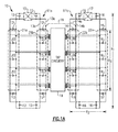
- FIG. 1A is a schematic diagram of one embodiment of an RTWO system 10.
- the RTWO system 10 includes a first elongated RTWO 11a, a second elongated RTWO 11b, and tap circuitry 19 that receives clock signal phases from both the first elongated RTWO 11a and from the second elongated RTWO 11b.
- the RTWO system 10 includes two RTWOs. However, the RTWO system 10 can include additional RTWOs, including, for example, 3 or more RTWOs.
- the first elongated RTWO 11a includes a differential transmission line including a first conductor 13a and a second conductor 13b.
- the first elongated RTWO 11a further includes a cross-over 15 and regeneration circuits 12.
- the second elongated RTWO 11b includes a differential transmission line including a first conductor 14a and a second conductor 14b.
- the second elongated RTWO 11b further includes a cross-over 17 and regeneration circuits 16.
- the first and second elongated RTWOs 11a, 11b each include one cross-over and fourteen regeneration circuits.
- the RTWO system can include additional RTWOs and/or other circuitry.
- an RTWO can include a differential transmission line connected in a closed loop, an odd number of one or more cross-overs, and a plurality of regeneration circuits electrically connected along a path of the differential transmission line. Additionally, each of the cross-overs can reverse the polarity of a wave propagating along the differential transmission line, and the regeneration circuits can provide energy to the wave to compensate for the differential transmission line's losses. Additional details of RTWOs can be as described in U.S. Patent No. 6,556,089 .
- a phase-locking conductor 18 electrically connects a portion of the first conductor 13a of the first elongated RTWO 11a and a portion of the second conductor 14b of the second elongated RTWO 11b.
- a phase difference between the first and second elongated RTWOs 11a, 11b can be controlled by selecting a position on the first conductor 13a and a position on the second conductor 14b between which the phase-locking conductor 18 connects.
- other configurations are possible, including, for example, implementations in which the first and second elongated RTWOs 11a, 11b are phase-locked in other ways.
- the first elongated RTWO 11a is elongated in a first direction (vertically in Figure 1A ).
- the differential transmission line 13a, 13b of the first elongated RTWO 11a includes a first elongated section 21a and a second elongated section 21b that provide clock signal phases of high phase linearity to the tap circuitry 19.
- the first elongated section 21a is on a first side of the first elongated RTWO 11a
- the second elongated section 21b is on a second side of the first elongated RTWO 11a that is opposite the first side.
- the second elongated RTWO 11b is also elongated in the first direction.
- the differential transmission line 14a, 14b of the second elongated RTWO 11b includes a first elongated section 22a and a second elongated section 22b that provide clock signal phases of high phase linearity to the tap circuitry 19.
- the first elongated section 22a is on a first side of the second elongated RTWO 11b
- the second elongated section 22b is on a second side of the second elongated RTWO 11b that is opposite the first side.
- the illustrated embodiment includes RTWOs implemented with elongated sections of differential transmission line, which provide clock signal phases of relatively high phase linearity.
- the elongated sections 21a, 21b of the first elongated RTWO 11a and the elongated sections 22a, 22b of the second elongated RTWO 11b are relatively long in length and are substantially straight, and thus have relatively uniform capacitance loading.
- sections of a differential transmission line that have non-uniformities in length and/or thickness can have comparatively poor phase linearity.
- the clock signal phases provided by the first and second elongated RTWOs 11a, 11b have a phase non-linearity of less than about 10%.
- the wave velocity along the elongated sections 21 a, 21b of the first elongated RTWO 11a and the elongated sections 22a, 22b of the second elongated RTWO 11b is substantially constant.
- the wave can have a substantially constant wave velocity. Maintaining constant wave velocity along the elongated sections of the first and second elongated RTWO's enhances the phase linearity of clock signal phases generated using the elongated sections.
- an RTWO is elongated to have a length x1 in a first direction that is in the range of about 100 ⁇ m to 1000 ⁇ m and a width x2 in a second direction perpendicular to the first direction that is in the range of about 10 ⁇ m to about 500 ⁇ m.
- the length x1 is greater than the width x2 by a factor of 2 or more.
- the elongated sections 21 a, 21b of the first elongated RTWO 11a and the elongated sections 22a, 22b of the second elongated RTWO 11b have a length x3 in the range of about 90 ⁇ m to 900 ⁇ m. Although one example range of the length x3 has been provided, other lengths are possible, such as a length selected based on application and/or implementation.
- each elongated section can provide more than 90° of clock signal phases, including 45° or more of phase from each of the differential transmission line's conductors.
- the elongated sections 21 a, 21b of the first elongated RTWO 11a and the elongated sections 22a, 22b of the second elongated RTWO 11b each provide more than 130° of phase.
- the RTWOs are phase-locked such that the elongated sections provide clock signal phases across the full 360° range.
- the taps exhibit excellent linearity, since the straight transmission line sections avoid the curves, corners, and/or cross-overs associated with poor phase linearity performance.
- the illustrated configuration advantageously taps the first elongated RTWO 11a from the elongated sections 21 a, 21b and taps the second elongated RTWO 11b from the elongated sections 22a, 22b.
- the tap circuitry 19 receives clock signal phases from portions of the RTWOs 11a, 11b having relatively high phase linearity.
- the tap circuitry 19 avoids operating using clock signal phases generated from portions of transmission line near corners, curves, and/or cross-overs, which can have comparatively poor phase linearity.
- the elongated sections 21a, 21b of the first elongated RTWO 11a and the elongated sections 22a, 22b of the second elongated RTWO 11b do not include any curves, corners, or cross-overs.
- the tap circuitry 19 does not receive any clock signal phases from the first elongated RTWO 11a from outside the elongated sections 21a, 21b.
- the tap circuitry 19 does not receive any clock signal phases from the second elongated RTWO 11b that are outside of the elongated sections 22a, 22b. Configuring the RTWO system 10 in this manner provides clock signal phases of high linearity to the tap circuitry 19.
- the tap circuitry 19 receives clock signal phases from two elongated sections 21a, 21b of the first elongated RTWO 11a and from two elongated sections 22a, 22b of the second elongated RTWO 11b.
- other configurations are possible.
- four elongated RTWOs are phase-locked, and one elongated section of transmission line from each of the four RTWOs is used to generate clock signal phases for tap circuitry.
- Using more than two elongated RTWOs provides averaging that can reduce phase noise and/or reduce components of nonlinearity having a random nature. Further, in such configurations, clock signal phases can be used from the center of elongated sections of the RTWOs while still providing clock signal phases that span the full 360°. Thus, configurations using three or more elongated RTWOs can further increase linearity relative to a configuration using two elongated RTWOs.
- Figure 1A illustrates the tap circuitry 19 as being positioned between the first and second elongated RTWOs 11a, 11b
- the tap circuitry 19 is integrated in a layout of the first and second elongated RTWOs 11a, 11b.
- long wires can be used to route distant clock signal phases to tap circuitry, long wires can also degrade phase linearity, reduce quality factor (Q-factor), and/or otherwise degrade the RTWO system's performance.
- transistors of the tap circuitry 19 used for tapping are positioned in close proximity to the differential transmission lines of the first and second elongated RTWOs 11a, 11b.
- the transistors of the tap circuitry 19 can include uniform layouts associated with high phase linearity.
- the layout the tap circuitry's transistors can be uniform, even when the RTWO system 10 is fabricated using a process that includes design rules constraining transistor layouts to be orthogonal.
- an RTWO that includes taps along the entirety of the RTWO's transmission line can include non-uniform transistor layouts.
- the layout of transistors used for tapping near curves of the RTWO may have non-uniform layouts relative to transistors used for tapping along straight-sides of an RTWO.
- the first and second elongated RTWOs 11a, 11b are phase-locked with a non-zero phase shift. Phase-locking the first and second elongated RTWOs 11a, 11b in this manner can provide clock signal phases to the tap circuitry 19 that span 360°. In contrast, when two RTWOs are phase-locked with a zero degree shift, the elongated sections of the RTWOs can produce redundant clock signal phases for tap circuitry.
- the illustrated configuration advantageously includes a phase-shift to increase the number of different clock signal phases available to the tap circuitry 19. The amount of phase shift between the phase-locked RTWOs 11a, 11b can control the angular separation of the clock signal phases provided by the first elongated RTWO 11a and the clock signal phases provided by the second elongated RTWO 11b.
- the first and second elongated RTWOs 11a, 11b are phase-locked by a phase shift ⁇ that is selected to be in the range of about 35° and 55°.
- a phase shift between RTWOs can be selected based on application and/or implementation.
- FIG 1B is a schematic diagram of another embodiment of an RTWO system 30.
- the RTWO system 30 of Figure 1B is similar to the RTWO system 10 Figure 1A , except that the RTWO system 30 illustrates a specific implementation in which a phase-locking conductor 28 is used to phase-lock the second elongated RTWO 11b to the first elongated RTWO 11a with a 45° phase shift.
- the illustrated RTWO system 30 has been annotated to include phases of various clock signal phases along the transmission lines of the first and second elongated RTWOs 11a, 11b. Although one example of clock signal phases is shown in Figure 1B , other clock signal phases are possible, including, for example, clock signal phases associated with a particular RTWO system implementation.
- the tap circuitry 19 receives clock signal phases of 108°, 126°, 144°, 162°, 288°, 306°, 324°, and 342° from the first elongated section 21a of the first elongated RTWO 11a. Additionally, the tap circuitry 19 receives clock signal phases of 18°, 36°, 54°, 72°, 198°, 216°, 234°, and 252° from the second elongated section 21b of the first elongated RTWO 11b.
- the tap circuitry 19 receives clock signal phases of 63°, 81°, 99°, 117°, 243°, 261°, 279°, and 297° from the first elongated section 22a of the second elongated RTWO 11b. Additionally, the tap circuitry 19 receives clock signal phases of 9°, 27°, 153°, 171°, 189°, 207°, 333°, and 353° from the second elongated section 22b of the second elongated RTWO 11b.
- the tap circuitry 19 receives clock signal phases of 9°, 18°, 27°, 36°, 54°, 63°, 72°, 81°, 99°, 108°, 117°, 126°, 144°, 153°, 162°, 171°, 189°, 198°, 207°, 216°, 234°, 243°, 252°, 261°, 279°, 288°, 297°, 306°, 324°, 333°, 342°, and 353° from elongated sections of the first and second elongated RTWOs 11a, 11b.
- the elongated sections provide clock signal phases across the full 360° range.
- the taps exhibit excellent linearity, since the elongated sections include substantially straight sections of transmission line, and thus avoid the curves, corners, and/or cross-overs associated with poor phase linearity performance.
- the largest phase separation between clock signal phases of adjacent taps is about 18°.
- additional taps can be provided to reduce the largest phase separation.
- the largest phase separation between clock signal phases of adjacent taps is less than about 0.35°.
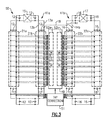
- FIG. 2 is a schematic diagram of another embodiment of an RTWO system 40.
- the RTWO system 40 includes a first elongated RTWO 41a, a second elongated RTWO 41b, and tap circuitry 39 that receives clock signal phases from both the first elongated RTWO 41a and from the second elongated RTWO 41b.
- the RTWO system 40 of Figure 2 is similar to the RTWO system 10 of Figure 1A , except that the RTWO system 40 of Figure 2 includes a configuration in which the tap circuitry 39 receives a greater number of clock signal phases from the first and second elongated RTWOs 41a, 41b relative to the configuration shown in Figure 1A .
- the tap circuity 39 receives 80 total clock signal phases from the first and second elongated RTWOs 41a, 41b.
- FIG. 2 illustrates a configuration in which tap circuitry receives 80 clock signal phases
- tap circuitry can receive more or fewer clock signals phases. In one embodiment, tap circuitry receives about 1024 clock signal phases.
- the number of taps of an RTWO system can be important in a variety of applications. For instance, in frequency synthesizer applications, a number of available frequencies for synthesis depends on a number of available RTWO phases, and thus on the density of the RTWO's taps. Additionally, in ADC applications, the resolution of the ADC depends on the RTWO tap density.
- additional taps can be added to the RTWO system 40 by tapping the differential transmission lines of the first and second elongated RTWOs 41a, 41b in a greater number of positions.
- tapping the transmission lines in additional locations can increase tap density, such an approach can be limited by a variety of constraints, including, for example, available layout resources. For instance, a number of available metal routes can limit the maximum number of taps that an RTWO can provide.
- an RTWO system can employ phase interpolation to increase a number of available clock signal phases beyond those obtained by tapping transmission lines.
- Figure 2 omits illustrating regeneration circuits in the elongated sections 21a, 21b of the first elongated RTWO 41a and in the elongated sections 22a, 22b of the second elongated RTWO 41b.
- the elongated sections of the first and second elongated RTWOs 41 a, 41b can include regeneration circuits.
- FIG 3 is a schematic diagram of another embodiment of an RTWO system 50.
- the RTWO system 50 includes the first elongated RTWO 41a and the second elongated RTWO 41b, which can be as described earlier.
- the RTWO system 50 further includes tap circuitry 49 and a tap correction circuit 51.
- the tap circuitry 49 includes a first tap shifting circuit 52a and a second tap shifting circuit 52b.
- the first and second tap shifting circuits 52a, 52b can be used to shift or adjust the taps of the first and second elongated RTWOs 41a, 41b, respectively, to compensate for a phase-locking error of the first and second elongated RTWOs 41a, 41b.
- the first and second elongated RTWOs 41a, 41b may have been designed to lock with a phase shift ⁇ , but the elongated RTWOs 41a, 41b may lock with a phase shift ⁇ + ⁇ , where ⁇ is the phase-locking error or phase mismatch.
- the phase mismatch can arise from a variety of sources, such as manufacturing errors, and can vary with operating conditions, including temperature and/or voltage.
- the first and second tap shifting circuits 52a, 52b aid in correcting for a phase mismatch between the first and second elongated RTWOs 41a, 41b relative to a desired phase shift, thereby aiding the tap circuitry in combining the clock signal phases from the first elongated RTWO 41a and the clock signal phases from the second elongated RTWO 41b to generate output clock signal phases.
- Figure 3 illustrates a configuration in which the tap circuitry 49 includes two tap shifting circuits
- other configurations are possible, including, for example, implementations including a single tap shifting circuit.
- tap correction circuitry can be placed in other locations.
- an RTWO system includes two or more tap correction circuits.
- the tap correction circuit 51 generates a tap shifting control signal that is used to control tap shifting of the first and second tap shifting circuits 49.
- the tap correction circuit 51 receives at least one clock signal phase from the first elongated RTWO 41a and at least one clock signal phase from the second elongated RTWO 41b, and generates the tap shifting control signal based on a comparison of the clock signal phases.
- a tap shifting circuit is used to shift a tap by a discrete number of tap positions.
- the tap correction circuit 51 receives clock signal phases from the first and second elongated RTWOs 41a, 41b. However, in contrast to the tap circuitry 49 that receives clock signal phases from the elongated sections 21 a, 21b of the first elongated RTWO 41a and from the elongated sections 22a, 22b of the second elongated RTWO 41b, the illustrated tap correction circuit 51 receives clock signal phases generated outside the elongated sections.
- Configuring the RTWO system 50 in this manner increases the linearity of the elongated sections 50 relative to a configuration in which a tap correction circuit operates as a non-uniform load to the RTWOs' elongated sections. Moreover, implementing the tap correction circuit 51 near corners of the RTWOs 41a, 41b avoids using layout resources near the elongated sections of the first and second elongated RTWOs 41a, 41b. Accordingly, the illustrated configuration provides the benefits of both tap correction and high tap density.
- FIG 4A is a schematic diagram of another embodiment of an RTWO system 150.
- the RTWO system 150 includes the first elongated RTWO 41a and the second elongated RTWO 41b, which can be as described earlier.
- the RTWO system 150 further includes tap circuitry 159.
- the tap circuitry 159 includes a first phase interpolation circuit 162a and a second phase interpolation circuit 162b.
- the first phase interpolation circuit 162a interpolates between the clock signal phases provided by the first elongated RTWO 41a to generate additional clock signal phases.
- the second phase interpolation circuit 162b interpolates between the clock signal phases provide by the second elongated RTWO 41b to generate additional clock signal phases.
- the number of taps of an RTWO system can be important in a variety of applications. For instance, in frequency synthesizer applications, a number of available frequencies for synthesis depends on a number of available RTWO phases, and thus on the density of the RTWO's taps. Additionally, in ADC applications, the resolution of the ADC depends on the RTWO tap density.
- a transmission line can be tapped in additional locations to increase tap density, such an approach can be limited by a variety of constraints, including, for example, available layout resources.
- phase circuitry includes a common or shared phase interpolation circuit that interpolates clock signal phases from two or more RTWOs.
- the RTWO system 150 has a tap density of at least about 5.625 degrees/tap.
- RTWO system 150 Additional details of the RTWO system 150 can be as described earlier.
- Figure 4B is a schematic diagram 180 of one example of interpolated clock signals for an RTWO system, such as the RTWO system 150 of Figure 4A .
- the diagram 180 includes a first clock signal phase 181 and a second clock signal phase 182, which correspond to clock signal phases from two taps that are adjacent in phase.
- a phase interpolation circuit interpolates the first and second clock signal phases 181, 182 to generate interpolated clock signal phases 191-193.
- the phase interpolation circuit can provide both the first and second clock signal phases 181, 182 and the interpolated clock signal phase 191-193 as outputs.
- phase interpolation circuits can be included in tap circuitry to increase the number of available clock signal phases.
- Figure 4B illustrates an example in which three interpolated clock signal phases are generated by interpolation, other configurations are possible.
- a phase interpolation circuit generates between 1 and 64 interpolated clock signals between adjacent taps.
- the first clock signal phase 181 and the second clock signal phase 182 are generated by the same RTWO.
- the first clock signal phase 181 corresponds to the 18° phase from the first elongated RTWO 11a and the second clock signal phase 182 corresponds to the 36° phase from the first elongated RTWO 11a.
- the first clock signal phase 181 and the second clock signal phase 182 are generated by different RTWOs.
- the first clock signal phase 181 corresponds to the 18° phase from the first elongated RTWO 11a and the second clock signal phase 182 correspond to the 27° phase from the second elongated RTWO 11b.
- FIG. 5 is a schematic diagram of one embodiment of a phase interpolation system 200.
- the phase interpolation system 200 includes a differential transmission line 210 and a phase interpolation circuit 220.
- the differential transmission line 210 includes a first conductor 211 and a second conductor 211b.
- the first and second conductors 211 a, 211 b are substantially parallel to one another and extend in a first direction (vertically in Figure 5 ).
- the first conductor 211a has been tapped in three positions to generate a P N clock signal phase, a P N+1 clock signal phase, and a P N+2 clock signal phase.
- the second conductor 211b has been tapped in three positions to generate a P N_B clock signal phase, a P N+1_B clock signal phase, and a P N+2_B clock signal phase.
- the P N_B , P N+1_B , and P N+2_B clock signal phases are inverted or about 180° out of phase relative to the P N , P N+1 , and P N+2 clock signal phases, respectively.
- the differential transmission line 210 is a differential transmission line of an RTWO.
- the phase interpolation circuit 220 includes a first phase interpolator 221 and a second phase interpolator 222.
- the first phase interpolator 221 receives the P N , P N_B , P N+1 and P N+1_B clock signal phases, and generates a first group of output clock signal phases 225.
- each of the output clock signal phases 225 generated by the first interpolator 221 are interpolated clock signal phases.
- the clock signal phases 225 include not only interpolated clock signal phases, but also at least one of the P N , P N_B , P N+1 or P N+1_B clock signal phases.
- the second phase interpolator 222 receives the P N+1 , P N+1_B , P N+2 and P N+2_B clock signal phases, and generates a second group of output clock signal phases 226.
- the first and second phase interpolators 221, 222 provide phase interpolation to increase the number of available clock signal phases.
- the phase interpolators 221, 222 provide phase interpolation to provide a greater number of clock signal phases relative to the clock signal phases provided by tapping the differential transmission line 210.
- Figure 5 illustrates a configuration including two phase interpolators that receive clock signal phases based on tapping the first conductor 211a in three positions and the second conductor 211b in three positions
- an interpolation system includes between about 64 and about 1024 phase interpolators.
- Figure 5 illustrates a configuration in which a phase interpolator receives clock signal phases from both conductors of the differential transmission line 210
- other configurations are possible, such as implementations in which a phase interpolator receives clock signal phases from a single conductor.
- teachings herein are also applicable to configurations in which phase interpolators provide interpolation between clock signal phases generated by two or more different transmission lines.
- the phase interpolation circuit 220 includes phase interpolators 221, 222 that operate as capacitive loads to the differential transmission line 210. Additionally, the phase interpolators 221, 222 operate as part of the distributed capacitance of the differential transmission line 210.
- phase interpolators 221, 222 as capacitive loads to a transmission line decreases power consumption.
- the phase interpolators 221, 222 have an input capacitance, the interpolators operate without corresponding CV 2 f power loss, since the input capacitance operates as part of the characteristic impedance of the transmission line 210.
- a phase interpolator using resistive loads such as a resistor ladder, consumes CV 2 f power.
- the clock signal phases provided to the phase interpolators 221, 222 have a trapezoidal wavefront.
- edge rates of 30GV/s are achieved.
- phase interpolation system 200 can be as described earlier.
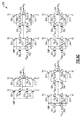
- FIG. 6A is a circuit diagram of one embodiment of a phase interpolator 230.
- the phase interpolator 230 includes a first capacitor 231, a second capacitor 232, and a third capacitor 233.
- the phase interpolator 230 receives a P N input clock signal phase and a P N+1 input clock signal phase and generates PH 1 , PH 2 , PH 3 , and PH 4 output clock signal phases.
- the first capacitor 231, the second capacitor 232, and the third capacitor 233 are electrically connected in series between a first node and a second node. As shown in Figure 6A , the first node is used both to receive the P N input clock signal phase and to generate the PH 1 output clock signal phase. Additionally, the second node is used to both receive the P N+1 input clock signal phase and to generate the PH 4 output clock signal phase. The PH 2 output clock signal phase is generated at a first intermediate node between the first and second capacitors 231, 232, and the PH 3 output clock signal phase is generated at a second intermediate node between the second and third capacitors 232, 233.
- Figure 6A illustrates a configuration of a phase interpolator that receives two clock signal phases and generates four clock signal phases
- the phase interpolator 230 can include more or fewer capacitors in series to generate a desired number of output clock signal phases.
- the phase interpolator 230 illustrates one example of a phase interpolator that operates as a capacitive load to a transmission line, and thus reduces or eliminates CV 2 f power loss.
- phase interpolator 230 Additional details of the phase interpolator 230 can be as described earlier.
- FIG. 6B is a circuit diagram of another embodiment of a phase interpolator 250.
- the phase interpolator 250 includes first to fourth precharge p-type field effect transistors (PFETs) 251-254 and first to fourth comparator n-type field effect transistors (NFETs) 261-264. Additionally, the phase interpolator 250 includes a first group of ratioed NFETs 271-273 and a second group of ratioed NFETs 281-283.
- the phase interpolator 250 receives a P N input clock signal phase and a P N+1 input clock signal phase and generates PH 1 , PH 2 , PH 3 , and PH 4 output clock signal phases.
- the gates of the precharge PFETs 251-254 receive an inverted precharge signal PCH_B, which is used to precharge the PH 1 , PH 2 , PH 3 , and PH 4 output clock signal phases to a voltage level V 2 .
- the gates of the precharge NFETs 261-264 receive a comparator signal CMP, which can be activated before a rising edge of the P N and P N+1 input clock signal phases is received.
- an RTWO that includes the phase interpolator 250 is used as a counter, and the comparator signal CMP is used to start and stop counting.
- various combinations of the first group of ratioed NFETs 271-273 and the second group of ratioed NFETs 281-283 are used to control timing of a falling edge of the PH 1 , PH 2 , PH 3 , and PH 4 output clock signal phases to a voltage level V 1 .
- the first group of ratioed NFETs 271-273 include gates that receive the P N input clock signal
- the second group of ratioed NFETs 281-283 include gates that receive the P N+1 input clock signal.
- the PH 1 output clock signal phase is generated using the NFET 271, which has a 4x weight in this example relative to a unit transistor of 1x size. Excluding a propagation delay through the phase interpolator 250, the PH 1 output clock signal phase can have a phase that is about equal to that of the P N input clock signal. Additionally, the PH 2 output clock signal phase is generated using the parallel combination of the NFET 272 and the NEFT 282, which have 3x and 1x weights, respectively, in this example. Excluding propagation delay, the PH 2 output clock signal phase can have a phase that is about one-quarter of the way between the phases of the P N and P N+1 input clock signals.
- the PH 3 output clock signal phase is generated using the parallel combination of the NFET 273 and the NEFT 283, which have 1x and 3x weights, respectively, in this example. Excluding propagation delay, the PH 3 output clock signal phase can have a phase that is about three-quarters of the way between the phases of the P N and P N+1 input clock signals. Additionally, the PH 4 output clock signal phase is generated using the NFET 281, which has a 4x weight in this example. Excluding propagation delay, the PH 4 output clock signal phase can have a phase that is about equal to that of the P N+1 input clock signal.
- ratioed FETs Although one example of ratioed FETs has been provided, other configurations are possible.
- a phase interpolator can include combinations of ratioed FETs to generate interpolated clock signal phases of desired phases.
- teachings herein are applicable to configurations using ratioed NFETs, ratioed PFETs, or a combination thereof.
- the phase interpolator 250 illustrates another example of a phase interpolator that operates as a capacitive load to a transmission line, and thus reduces or eliminates CV 2 f power loss.
- phase interpolator 250 Additional details of the phase interpolator 250 can be as described earlier.
- FIG. 6C is a circuit diagram of another embodiment of a phase interpolator 300.
- the phase interpolator 300 includes comparator PFETs 301-304, feedback PFETs 305-308, comparator NFETs 311-314, feedback NFETs 315-318, and inverters 361-364. Additionally, the phase interpolator 300 includes a first group of ratioed FETs 321-324, a second group of ratioed FETs 331-338, a third group of ratioed FETs 341-348, and a fourth group of ratioed FETs 351-358.
- the phase interpolator 300 receives a P N input clock signal phase, a P N_B input clock signal phase, a P N+1 input clock signal phase, and a P N+1_B input clock signal phase and generates PH 1 , PH 2 , PH 3 , and PH 4 output clock signal phases.
- the gates of the comparator PFETs 301-304 and the gates of the comparator NFETs 311-314 receive a comparator signal CMP.
- an RTWO that includes the phase interpolator 300 is used as a counter, and the comparator signal CMP is used to start and stop counting.
- the first to fourth inverters 361-364 generate the PH 1 , PH 2 , PH 3 , and PH 4 output clock signal phases, respectively. Additionally, the inverters 361-364 provide feedback to the gates of the feedback PFETs 305-308 and the gates of the feedback NFETs 315-318. Providing feedback allows the output clock signal phases to control timing of precharge operations, thereby avoiding a need for a global precharge signal.
- the first group of ratioed FETs 321-324 is used to control timing of the PH 1 output clock signal phase.
- the first group of ratioed FETs 321-324 includes a PFET 321 and an NFET 322 that operate in a first stage and a PFET 323 and an NFET 324 that operate in a second stage.
- the PFET 321 and the NFET 324 receive the P N input clock signal phase and have a 4x weight
- the NFET 322 and the NFET 323 receive the P N_B input clock signal phase and have a 4x weight.
- the PH 1 output clock signal phase can have a phase that is about equal to that of the P N input clock signal.
- the second group of ratioed FETs 331-338 is used to control timing of the PH 2 output clock signal phase.
- the second group of ratioed FETs 331-338 includes a PFET 331 of 1x weight, an NFET 332 of 1x weight, a PFET 333 of 3x weight, and an NFET 334 of 3x weight that operate in a first stage. Additionally, the second group of ratioed FETs 331-338 includes a PFET 335 of 1x weight, an NFET 336 of 1x weight, a PFET 337 of 3x weight, and an NFET 338 of 3x weight that operate in a second stage.
- the PFET 333 and the NFET 338 receive the P N input clock signal phase
- the NFET 334 and the PFET 337 receive the P N_B input clock signal phase
- the PFET 331 and the NFET 336 receive the P N+1 input clock signal phase
- the NFET 332 and the PFET 335 receive the P N+1_B input clock signal phase.
- the PH 2 output clock signal phase can have a phase that is about one-quarter of the way between the phases of the P N and P N+1 input clock signals.
- the third group of ratioed FETs 341-348 is used to control timing of the PH 3 output clock signal phase.
- the third group of ratioed FETs 341-348 includes a PFET 341 of 2x weight, an NFET 342 of 2x weight, a PFET 343 of 2x weight, and an NFET 344 of 2x weight that operate in a first stage. Additionally, the third group of ratioed FETs 341-348 includes a PFET 345 of 2x weight, an NFET 346 of 2x weight, a PFET 347 of 2x weight, and an NFET 348 of 2x weight that operate in a second stage.
- the PFET 343 and the NFET 348 receive the P N input clock signal phase
- the NFET 344 and the PFET 347 receive the P N_B input clock signal phase
- the PFET 341 and the NFET 346 receive the P N+1 input clock signal phase
- the NFET 342 and the PFET 345 receive the P N+1_B input clock signal phase.
- the PH 3 output clock signal phase can have a phase that is about half of the way between the phases of the P N and P N+1 input clock signals.
- the fourth group of ratioed FETs 351-358 is used to control timing of the PH 4 output clock signal phase.
- the fourth group of ratioed FETs 351-358 includes a PFET 351 of 3x weight, an NFET 352 of 3x weight, a PFET 353 of 1x weight, and an NFET 354 of 1x weight that operate in a first stage. Additionally, the fourth group of ratioed FETs 351-358 includes a PFET 355 of 3x weight, an NFET 356 of 3x weight, a PFET 357 of 1x weight, and an NFET 358 of 1x weight that operate in a second stage.
- the PFET 353 and the NFET 358 receive the P N input clock signal phase
- the NFET 354 and the PFET 357 receive the P N_B input clock signal phase
- the PFET 351 and the NFET 356 receive the P N+1 input clock signal phase
- the NFET 352 and the PFET 355 receive the P N+1 B input clock signal phase.
- the PH 4 output clock signal phase can have a phase that is about three-quarters of the way between the phases of the P N and P N+1 input clock signals.
- phase interpolator can include combinations of ratioed FETs to generate interpolated clock signal phases of desired phases.
- the phase interpolator 300 illustrates another example of a phase interpolator that operates as a capacitive load to a transmission line, and thus reduces or eliminates CV 2 f power loss.
- phase interpolator 300 can be as described earlier.
- FIG. 7 is a schematic diagram of a frequency synthesizer 500 including an RTWO system according to one embodiment.
- the frequency synthesizer 100 includes a phase-frequency detector (PFD) 501, a loop filter 502, an RTWO system 503, a feedback divider 504, and a phase selection circuit 505.
- the frequency synthesizer 500 receives a reference clock signal f REF and generates a plurality of synthesized clock signals f 1 , f 2 , ... f n , which can have different frequencies and/or phases from one another.
- PFD phase-frequency detector
- the frequency synthesizer 500 illustrates one example of an electronic system that can include an RTWO system implemented in accordance with the teachings herein.
- the RTWO systems herein can be used in other configurations of electronic systems.
- the PFD 501 generates an error signal based on comparing the reference clock signal f REF to a feedback clock signal f FBK generated by the feedback divider 504.
- the loop filter 502 generates a filtered error signal based on filtering the error signal from the PFD 501.
- the loop filter 502 controls an oscillation frequency of the RTWO system 503 using the filtered error signal.
- the loop filter 502 can control the oscillation frequency of the RTWO system 503 in a variety of ways, including, for example, by controlling the capacitance of shunt capacitors of the RTWO system's transmission lines.
- the RTWO system 503 includes tap circuitry (not illustrated in Figure 7 ) that generates a plurality of clock signal phases for the phase selection circuit 505.
- the phase selection circuit 505 generates n synthesized output clock signals f 1 , f 2 , ... f n using digital selection techniques.
- one or more of the clock signal phases from the RTWO system 503 can be provided to the feedback divider 504, which generates the feedback clock signal f FBK of divided frequency.
- the illustrated frequency synthesizer 500 is implemented as a Doppler synthesizer, which can exhibit spurious output frequencies when the clock signal phases received by the phase selection circuit 505 have poor linearity. Additionally, a phase separation between the clock signal phases provides a fundamental limit on the synthesizer's RMS output jitter.
- the phase selection circuit 505 can be provided with a relatively large number of clock signal phases of relatively high phase linearity.
- the frequency synthesizer 500 can operate with relatively small clock jitter and/or output spurs.
- FIG 8 is a schematic diagram of an analog-to-digital converter (ADC) 510 including an RTWO system according to one embodiment.
- the ADC 510 includes an input switch 511, an integrator 512, a comparator 513, and a counter 514 that include an RTWO system 515.
- the ADC 510 receives an analog input signal at an input ADC IN and generates a digital output signal at an output ADC OUT .
- the ADC 510 illustrates one example of an electronic system that can include an RTWO system implemented in accordance with the teachings herein.
- the RTWO systems herein can be used in other configurations of electronic systems.
- the switch 511 is used to selectively couple the input ADC IN to the integrator 512.
- the integrator 512 includes an integration capacitor 521 and a resistor 522, and can be used to integrate an analog input voltage received on the input ADC IN .
- the ADC 510 can be implemented in a wide variety of configurations, including for example, as a single-slope ADC or a dual-slope ADC.
- the ADC 510 an input voltage received on the input ADC IN is integrated using the integrator 512, and the integrator's output is compared to a known reference value using the comparator 513. Additionally, the counter 514 is used to measure an integration time and/or deintegration time of the integrator 512.
- the illustrated counter 514 includes the RTWO 515.
- the accuracy of the counter 514 is based on the density of taps of the RTWO system 515.
- the RTWO system 515 includes N evenly-spaced taps and oscillates with a period of Tosc
- the counter 514 can be used to count in time increments of Tosc/N.
- the counter 514 can be provided with a relatively large number of clock signal phases of relatively high phase linearity.
- the ADC 510 can operate with relatively high linearity and/or resolution.
- ADC 510 Additional details of the ADC 510 can be as described earlier.
- Examples of the electronic devices can include, but are not limited to, consumer electronic products, parts of the consumer electronic products, electronic test equipment, etc. Examples of the electronic devices can also include circuits of optical networks or other communication networks.
- the consumer electronic products can include, but are not limited to, an automobile, a camcorder, a camera, a digital camera, a portable memory chip, a washer, a dryer, a washer/dryer, a copier, a facsimile machine, a scanner, a multifunctional peripheral device, etc.
- the electronic device can include unfinished products, including those for industrial, medical and automotive applications.
- Example 1 is an apparatus comprising: a rotary traveling wave oscillator (RTWO) system comprising: a first elongated RTWO comprising a first differential transmission line in a closed loop, wherein the first differential transmission line comprises one or more elongated sections that generate a first plurality of clock signal phases; a second elongated RTWO comprising a second differential transmission line in a closed loop, wherein the second differential transmission line comprises one or more elongated sections that generate a second plurality of clock signal phases, wherein the second elongated RTWO is phase-locked to the first elongated RTWO with a phase shift; and tap circuitry configured to receive the first plurality of clock signal phases from the first elongated RTWO and the second plurality of clock signal phases from the second elongated RTWO.
- a rotary traveling wave oscillator (RTWO) system comprising: a first elongated RTWO comprising a first differential transmission line in a closed loop, wherein the first differential transmission
- Example 2 can further include the tap circuitry further comprising a phase interpolation circuit configured to generate a plurality of interpolated clock signal phases based on interpolating between two or more clock signal phases received by the tap circuitry.
- the tap circuitry further comprising a phase interpolation circuit configured to generate a plurality of interpolated clock signal phases based on interpolating between two or more clock signal phases received by the tap circuitry.
- Example 3 can further include the phase interpolation circuit comprising a first interpolator comprising a plurality of capacitors electrically connected in series.
- Example 4 can further include the phase interpolation circuit comprising a first interpolator comprising a plurality of ratioed field effect transistors (FETs).
- FETs ratioed field effect transistors
- any one of Examples 1 to 4 can further include the one or more elongated sections of the first and second elongated RTWOs not including any curves, corners, or cross-overs.
- any one of Examples 1 to 5 can further include the tap circuity comprising one or more tap shifting circuits configured to compensate for a phase mismatch between the first elongated RTWO and the second elongated RTWO, wherein the RTWO system further comprises a tap correction circuit configured to control the one or more tap shifting circuits based on comparing one or more clock signals from the first elongated RTWO to one or more clock signal phases from the second elongated RTWO.
- Example 6 can further include the one or more clock signal phases from the first elongated RTWO being provided from outside of the one or more elongated sections of the first differential transmission line, and wherein the one or more clock signal phases from the second elongated RTWO are provided from outside of the one or more elongated sections of the second differential transmission line.
- any one of Examples 1 to 7 can further include the phase shift being selected to be in the range of about 35° and 55°.
- any one of Examples 1 to 8 can further include the one or more elongated sections of the first elongated RTWO extending in a first direction, wherein the one or more elongated section of the first elongated RTWO each have a length in the range of about 90 ⁇ m to 900 ⁇ m.
- any one of Examples 1 to 9 can further include the first elongated RTWO being elongated in a first direction, wherein the first elongated RTWO has a length in the first direction and a width in a second direction perpendicular to the first direction, wherein the length is greater than the width by a factor of 2 or more.
- any one of Examples 1 to 10 can further include the one or more elongated sections of the first differential transmission line comprising a first elongated section on a first side of the first elongated RTWO and a second elongated section on a second side of the first elongated RTWO that is opposite the first side, and wherein the one or more elongated sections of the second differential transmission line comprises a first elongated section on a first side of the second elongated RTWO and a second elongated section on a second side of the second elongated RTWO opposite the first side.
- any one of Examples 1 to 11 can further include a phase-locking conductor configured to phase lock the second elongated RTWO to the first elongated RTWO.
- any one of Examples 1 to 12 can further include a frequency synthesizer comprising the RTWO system, wherein the frequency synthesizer generates one or more synthesized clock signals based on a plurality of output clock signal phases of the tap circuitry.
- any one of Examples 1 to 13 can further include an analog-to-digital converter (ADC) comprising the RTWO system, wherein timing of a counting operation of the ADC is controlled by a plurality of output clock signal phases of the tap circuitry.
- ADC analog-to-digital converter
- Example 15 is an electronically-implemented method of electronic oscillation, the method comprising: phase-locking a first elongated rotary traveling wave oscillator (RTWO) to a second elongated RTWO with a phase shift; generating a first plurality of clock signal phases using one or more elongated sections of a first differential transmission line of the first elongated RTWO; generating a second plurality of clock signal phases using one or more elongated sections of a second differential transmission line of the second elongated RTWO; and providing the first plurality of clock signal phases and the second plurality of clock signal phases to tap circuitry.
- RTWO elongated rotary traveling wave oscillator
- Example 15 can further include generating a plurality of interpolated clock signal phases based on interpolating between two or more clock signal phases received by the tap circuitry.
- Example 17 is a phase interpolation system comprising: a transmission line; and a phase interpolation circuit comprising: a plurality of phase interpolators comprising a first phase interpolator configured to receive a plurality of input clock signal phases, wherein the plurality of input clock signal phases comprises a first input clock signal phase taken from a first position along the transmission line and a second input clock signal phase taken from a second position along transmission line, wherein the first phase interpolator is configured to generate one or more interpolated clock signal phases by interpolating between the first input clock signal phase and the second input clock signal phase.
- Example 17 can further include the plurality of phase interpolators operating as a distributed capacitive load of the transmission line.
- Example 17 or 18 can further include the first phase interpolator comprising a plurality of capacitors electrically connected in series.
- Example 17 or 18 can further include the first phase interpolator comprising a plurality of ratioed field effect transistors (FETs).
- FETs ratioed field effect transistors
- any one of Examples 17 to 20 can further include the transmission line comprising a differential transmission line electrically connected in a closed loop, wherein the differential transmission line comprises an odd number of one or more cross-overs, wherein each of the one or more cross-overs is configured to reverse the polarity of a wave propagating along the differential transmission line.
Landscapes
- Engineering & Computer Science (AREA)
- Theoretical Computer Science (AREA)
- Physics & Mathematics (AREA)
- General Engineering & Computer Science (AREA)
- General Physics & Mathematics (AREA)
- Stabilization Of Oscillater, Synchronisation, Frequency Synthesizers (AREA)
- Design And Manufacture Of Integrated Circuits (AREA)
- Manipulation Of Pulses (AREA)
Abstract
Description
- Embodiments of the invention relate to electronic systems, and more particularly, to rotary traveling wave oscillators.
- Multiphase oscillators can be used in a variety of applications, including, for example, telecommunications, optical networks, radar systems, and/or chip-to-chip communication. For instance, a multiphase oscillator can be included in a frequency synthesizer to generate an output clock signal that has a controlled phase and frequency relationship relative to a reference clock signal. Multiphase oscillators can also be used in data converters, such as analog-to-digital converters (ADCs).
- There is a need for improved multiphase oscillators.
- In one aspect, an apparatus including a rotary traveling wave oscillator (RTWO) system is provided. The RTWO system includes a first elongated RTWO including a first differential transmission line in a closed loop, and the first differential transmission line includes one or more elongated sections that generate a first plurality of clock signal phases. The RTWO system further includes a second elongated RTWO including a second differential transmission line in a closed loop, and the second differential transmission line includes one or more elongated sections that generate a second plurality of clock signal phases. The second elongated RTWO is phase-locked to the first elongated RTWO with a phase shift. The RTWO system further includes tap circuitry configured to receive the first plurality of clock signal phases from the first elongated RTWO and the second plurality of clock signal phases from the second elongated RTWO.
- In another aspect, an electronically implemented method of electronic oscillation is provided. The method includes phase-locking a first elongated RTWO to a second elongated RTWO with a phase shift, generating a first plurality of clock signal phases using one or more elongated sections of a first differential transmission line of the first elongated RTWO, generating a second plurality of clock signal phases using one or more elongated sections of a second differential transmission line of the second elongated RTWO, and providing the first plurality of clock signal phases and the second plurality of clock signal phases to tap circuitry.
- In another aspect, a phase interpolation system is provided. The phase interpolation system includes a transmission line and a phase interpolation circuit. The phase interpolation circuit includes a plurality of phase interpolators included a first phase interpolator configured to receive a plurality of input clock signal phases. The plurality of input clock signal phases includes a first input clock signal phase taken from a first position along the transmission line and a second input clock signal phase taken from a second position along transmission line. The first phase interpolator is configured to generate one or more interpolated clock signal phases by interpolating between the first input clock signal phase and the second input clock signal phase.
-
-
Figure 1A is a schematic diagram of one embodiment of rotary traveling wave oscillator (RTWO) system. -
Figure 1B is a schematic diagram of another embodiment of an RTWO system. -
Figure 2 is a schematic diagram of another embodiment of an RTWO system. -
Figure 3 is a schematic diagram of another embodiment of an RTWO system. -
Figure 4A is a schematic diagram of another embodiment of an RTWO system. -
Figure 4B is a schematic diagram of one example of interpolated clock signals for an RTWO system. -
Figure 5 is a schematic diagram of one embodiment of a phase interpolation system. -
Figure 6A is a circuit diagram of one embodiment of a phase interpolator. -
Figure 6B is a circuit diagram of another embodiment of a phase interpolator. -
Figure 6C is a circuit diagram of another embodiment of a phase interpolator. -
Figure 7 is a schematic diagram of a frequency synthesizer including an RTWO system according to one embodiment. -
Figure 8 is a schematic diagram of an analog-to-digital converter (ADC) including an RTWO system according to one embodiment. - The following detailed description of embodiments presents various descriptions of specific embodiments of the invention. However, the invention can be embodied in a multitude of different ways as defined and covered by the claims. In this description, reference is made to the drawings where like reference numerals may indicate identical or functionally similar elements.
- A rotary traveling wave oscillator (RTWO) is a type of electronic oscillator that includes a differential transmission line connected in a closed loop, an odd number of one or more cross-overs, and a plurality of regeneration circuits electrically connected along a path of the differential transmission line. Additionally, each of the cross-overs reverses the polarity of a wave propagating along the differential transmission line, and the regeneration circuits provide energy to the wave to compensate for the differential transmission line's losses. Additional details of RTWOs can be as described in commonly-owned
U.S. Patent No. 6,556,089, issued April 29, 2003 , and titled "ELECTRONIC CIRCUITRY,". - As persons having ordinary skill in the art will appreciate, clock signal phase can represent a fraction of a complete clock signal cycle elapsed as measured from a specified reference point. For clarity of the description, a clock signal phase local to a certain position along a transmission line may be referred to herein as having a phase of about 0°. However, skilled artisans will appreciate that clock signal phase can be defined relative to other reference points.
- In an RTWO, a traveling wave propagates along a differential transmission line. By tapping the differential transmission line at various positions, clock signals of different phases can be obtained. In one example, a tap circuit, such as an inverter or amplifier, can include an input electrically connected to a particular position of the differential transmission line to obtain a clock signal having a desired phase.
- In certain implementations, a differential transmission line can include taps that are spaced apart or spread out substantially evenly along the transmission line. For instance, tapping an RTWO using n tap circuits that are evenly spaced along the transmission line can be used to generate clock signals that are ideally spaced in phase by about 360/n degrees (°).
- The phase linearity of an RTWO's taps can be an important performance specification. In one example, an RTWO is included in a frequency synthesizer, and the RTWO's phase linearity impacts the frequency synthesizer's jitter and/or spectral purity of synthesized output clock signals. In another example, an RTWO is included in an analog-to-digital converter (ADC), and the RTWO's phase linearity impacts the ADC's linearity and/or resolution.
- The number or density of taps of an RTWO can also be important for a variety of applications. For instance, a frequency synthesizer can include an RTWO that is integer locked to a low noise reference clock signal, and output clock signals of desired frequencies can be synthesized by selecting phases of the RTWO using, for instance, a digital phase selection circuit. In such a system, a number of available frequencies for synthesis depends on a number of available RTWO phases, and thus on the density of the RTWO's taps. In another example, an ADC can include an RTWO, and the resolution of the ADC depends on the density of taps of the RTWO.
- It can be difficult to implement an RTWO with a large number of taps and/or with taps having high phase linearity. For example, layout constraints, such as limitations in metal routing, can limit the maximum number of taps that an RTWO can provide. Additionally, a layout of an RTWO's differential transmission line can impact the phase linearity of the RTWO's taps. For example, corners and/or curves can generate transmission line non-uniformities, which can degrade phase linearity. Moreover, the RTWO's cross-overs can also impact phase linearity, since the cross-overs can operate as a non-uniformity to the traveling wave that propagates along the differential transmission line.
- Moreover, the phase linearity of an RTWO can be constrained by design rules of a manufacturing process used to fabricate the RTWO. For instance, a manufacturing process can include design rules specifying transistor layouts to be orthogonal. Thus, even if the layout of the RTWO's differential transmission line were circular, the layout of transistors used in the RTWO's regeneration circuits and/or tap circuitry may not match the curves of the RTWO. Accordingly, it can be difficult to implement an RTWO with a larger number of taps of high phase linearity.
- In certain configurations herein, an RTWO system includes a first elongated RTWO and a second elongated RTWO that are phase-locked to one another with a non-zero phase shift. The first and second elongated RTWOs each include a differential transmission line having a ring-shaped layout that is elongated in a first direction. Each of the ring-shaped layouts includes two elongated sections of differential transmission line having excellent phase linearity. For example, such long and straight sections of the differential transmission lines can have uniform capacitance loading and avoid non-uniformities in length and/or thickness associated with poor phase linearity. Moreover, such sections include uniform layouts for transistors used in regeneration circuits and/or tap circuits.
- Accordingly, using elongated RTWOs with relatively long and narrow transmission lines can provide sections of transmission line of comparatively good phase linearity. By locking two or more of such RTWOs at a non-zero phase difference, four or more elongated sections of transmission line with excellent linearity can be achieved. Each elongated section can provide more than 90° of clock signal phases. The RTWOs are phase-locked such that the elongated sections provide clock signal phases across the full 360° range. The taps exhibit excellent linearity, since the elongated sections include substantially straight sections of transmission line conductors, and thus avoid the curves, corners, and/or cross-overs associated with poor phase linearity performance.
- In certain configurations herein, phase interpolation between adjacent taps is used to increase the available number of clock signal phases. The phase interpolation can be achieved using, for example, capacitor and/or transistor mixing. The phase interpolation circuits can be used to provide interpolated phase taps by mixing proportions of adjacent taps. The inputs of the interpolation circuits are connected along different positions of the differential transmission lines. Although the interpolation circuits have an input capacitance, such circuits operate without corresponding CV2 f power loss, where C is capacitance, V is voltage and f is frequency, since the input capacitance operates as part of the characteristic impedance of the transmission line.
- The teachings herein can be used in a wide variety of applications. In one example, an ADC includes an RTWO system that provides the ADC with a relatively large number of clock signal phases of high phase linearity. The ADC can be implemented as, for example, a dual or single slope ADC, and the clock signal phases generated by the RTWO system control counting. In such a configuration, the phase linearity and/or density of taps control the linearity and/or resolution of the ADC.
- In another example, the RTWO system is included in a Doppler frequency synthesizer, which uses the clock signal phases generated by the RTWO system for frequency synthesis. For example, an output clock signal from the RTWO system can be integer-locked to a low phase noise reference signal, and the clock signal phases of the RTWO system can be processed using digital control to synthesize a variety of output clock signals of different frequencies and/or phases. A Doppler synthesizer can exhibit spurious output frequencies when the clock signal phases have poor linearity, and a phase separation between taps provides a fundamental limit on root mean square (RMS) output jitter. Accordingly, including an RTWO system with a large number of taps of high phase linearity in a Doppler frequency synthesizer can enhance performance by improving output spectral purity and/or reducing jitter.
-
Figure 1A is a schematic diagram of one embodiment of anRTWO system 10. TheRTWO system 10 includes a firstelongated RTWO 11a, a second elongatedRTWO 11b, and tapcircuitry 19 that receives clock signal phases from both the firstelongated RTWO 11a and from the second elongatedRTWO 11b. - In the illustrated configuration, the
RTWO system 10 includes two RTWOs. However, theRTWO system 10 can include additional RTWOs, including, for example, 3 or more RTWOs. - The first
elongated RTWO 11a includes a differential transmission line including afirst conductor 13a and asecond conductor 13b. The firstelongated RTWO 11a further includes a cross-over 15 andregeneration circuits 12. The second elongatedRTWO 11b includes a differential transmission line including afirst conductor 14a and asecond conductor 14b. The second elongatedRTWO 11b further includes across-over 17 andregeneration circuits 16. - In the illustrated embodiment, the first and second
elongated RTWOs - As persons having ordinary skill in the art will appreciate, an RTWO can include a differential transmission line connected in a closed loop, an odd number of one or more cross-overs, and a plurality of regeneration circuits electrically connected along a path of the differential transmission line. Additionally, each of the cross-overs can reverse the polarity of a wave propagating along the differential transmission line, and the regeneration circuits can provide energy to the wave to compensate for the differential transmission line's losses. Additional details of RTWOs can be as described in
U.S. Patent No. 6,556,089 . - As shown in
Figure 1A , a phase-lockingconductor 18 electrically connects a portion of thefirst conductor 13a of the firstelongated RTWO 11a and a portion of thesecond conductor 14b of the second elongatedRTWO 11b. In the illustrated configuration, a phase difference between the first and secondelongated RTWOs first conductor 13a and a position on thesecond conductor 14b between which the phase-lockingconductor 18 connects. However, other configurations are possible, including, for example, implementations in which the first and secondelongated RTWOs - As shown in
Figure 1A , the firstelongated RTWO 11a is elongated in a first direction (vertically inFigure 1A ). Thedifferential transmission line elongated RTWO 11a includes a firstelongated section 21a and a secondelongated section 21b that provide clock signal phases of high phase linearity to thetap circuitry 19. As shown inFigure 1A , the firstelongated section 21a is on a first side of the firstelongated RTWO 11a, and the secondelongated section 21b is on a second side of the first elongatedRTWO 11a that is opposite the first side. Additionally, the second elongatedRTWO 11b is also elongated in the first direction. Thedifferential transmission line RTWO 11b includes a firstelongated section 22a and a secondelongated section 22b that provide clock signal phases of high phase linearity to thetap circuitry 19. As shown inFigure 1A , the firstelongated section 22a is on a first side of the second elongatedRTWO 11b, and the secondelongated section 22b is on a second side of the second elongatedRTWO 11b that is opposite the first side. - The illustrated embodiment includes RTWOs implemented with elongated sections of differential transmission line, which provide clock signal phases of relatively high phase linearity. For example, the
elongated sections elongated RTWO 11a and theelongated sections RTWO 11b are relatively long in length and are substantially straight, and thus have relatively uniform capacitance loading. In contrast, sections of a differential transmission line that have non-uniformities in length and/or thickness can have comparatively poor phase linearity. In one embodiment, the clock signal phases provided by the first and secondelongated RTWOs - In the illustrated embodiment, the wave velocity along the
elongated sections elongated RTWO 11a and theelongated sections RTWO 11b is substantially constant. For example, when a traveling wave propagates along a substantially straight section of a differential transmission line with uniform loading, the wave can have a substantially constant wave velocity. Maintaining constant wave velocity along the elongated sections of the first and second elongated RTWO's enhances the phase linearity of clock signal phases generated using the elongated sections. - In one embodiment, an RTWO is elongated to have a length x1 in a first direction that is in the range of about 100 µm to 1000 µm and a width x2 in a second direction perpendicular to the first direction that is in the range of about 10 µm to about 500 µm. In one embodiment, the length x1 is greater than the width x2 by a factor of 2 or more. Although various examples of the dimensions x1 and x2 have been described, other lengths and widths are possible, such as those selected based on application and/or implementation.
- In one embodiment, the
elongated sections elongated RTWO 11a and theelongated sections RTWO 11b have a length x3 in the range of about 90 µm to 900 µm. Although one example range of the length x3 has been provided, other lengths are possible, such as a length selected based on application and/or implementation. - By phase-locking two or more elongated RTWOs with a non-zero phase difference, four or more sections of differential transmission line with high phase linearity can be achieved. Each elongated section can provide more than 90° of clock signal phases, including 45° or more of phase from each of the differential transmission line's conductors. In one embodiment, the
elongated sections elongated RTWO 11a and theelongated sections RTWO 11b each provide more than 130° of phase. The RTWOs are phase-locked such that the elongated sections provide clock signal phases across the full 360° range. The taps exhibit excellent linearity, since the straight transmission line sections avoid the curves, corners, and/or cross-overs associated with poor phase linearity performance. - Thus, the illustrated configuration advantageously taps the first
elongated RTWO 11a from theelongated sections RTWO 11b from theelongated sections tap circuitry 19 receives clock signal phases from portions of theRTWOs tap circuitry 19 avoids operating using clock signal phases generated from portions of transmission line near corners, curves, and/or cross-overs, which can have comparatively poor phase linearity. - For example, as shown in
Figure 1A , theelongated sections elongated RTWO 11a and theelongated sections RTWO 11b do not include any curves, corners, or cross-overs. Additionally, in the illustrated embodiment, thetap circuitry 19 does not receive any clock signal phases from the firstelongated RTWO 11a from outside theelongated sections tap circuitry 19 does not receive any clock signal phases from the second elongatedRTWO 11b that are outside of theelongated sections RTWO system 10 in this manner provides clock signal phases of high linearity to thetap circuitry 19. - In the illustrated configuration, the
tap circuitry 19 receives clock signal phases from twoelongated sections elongated RTWO 11a and from twoelongated sections RTWO 11b. However, other configurations are possible. For example, in another embodiment, four elongated RTWOs are phase-locked, and one elongated section of transmission line from each of the four RTWOs is used to generate clock signal phases for tap circuitry. - Using more than two elongated RTWOs provides averaging that can reduce phase noise and/or reduce components of nonlinearity having a random nature. Further, in such configurations, clock signal phases can be used from the center of elongated sections of the RTWOs while still providing clock signal phases that span the full 360°. Thus, configurations using three or more elongated RTWOs can further increase linearity relative to a configuration using two elongated RTWOs.
- Although
Figure 1A illustrates thetap circuitry 19 as being positioned between the first and secondelongated RTWOs tap circuitry 19 is integrated in a layout of the first and secondelongated RTWOs tap circuitry 19 used for tapping are positioned in close proximity to the differential transmission lines of the first and secondelongated RTWOs - Since the
tap circuitry 19 receives clock signal phases from theelongated sections elongated RTWO 11a and from the elongated sections of 22a, 22b of the second elongatedRTWO 11b, the transistors of thetap circuitry 19 can include uniform layouts associated with high phase linearity. Thus, the layout the tap circuitry's transistors can be uniform, even when theRTWO system 10 is fabricated using a process that includes design rules constraining transistor layouts to be orthogonal. - In contrast, an RTWO that includes taps along the entirety of the RTWO's transmission line can include non-uniform transistor layouts. For example, the layout of transistors used for tapping near curves of the RTWO may have non-uniform layouts relative to transistors used for tapping along straight-sides of an RTWO.
- With continuing reference to
Figure 1A , the first and secondelongated RTWOs elongated RTWOs tap circuitry 19 that span 360°. In contrast, when two RTWOs are phase-locked with a zero degree shift, the elongated sections of the RTWOs can produce redundant clock signal phases for tap circuitry. Thus, the illustrated configuration advantageously includes a phase-shift to increase the number of different clock signal phases available to thetap circuitry 19. The amount of phase shift between the phase-lockedRTWOs elongated RTWO 11a and the clock signal phases provided by the second elongatedRTWO 11b. - In one embodiment, the first and second
elongated RTWOs - Additional details of the
RTWO system 10 can be as described earlier. -
Figure 1B is a schematic diagram of another embodiment of anRTWO system 30. TheRTWO system 30 ofFigure 1B is similar to theRTWO system 10Figure 1A , except that theRTWO system 30 illustrates a specific implementation in which a phase-lockingconductor 28 is used to phase-lock the second elongatedRTWO 11b to the firstelongated RTWO 11a with a 45° phase shift. - The illustrated
RTWO system 30 has been annotated to include phases of various clock signal phases along the transmission lines of the first and secondelongated RTWOs Figure 1B , other clock signal phases are possible, including, for example, clock signal phases associated with a particular RTWO system implementation. - As shown in
Figure 1B , thetap circuitry 19 receives clock signal phases of 108°, 126°, 144°, 162°, 288°, 306°, 324°, and 342° from the firstelongated section 21a of the firstelongated RTWO 11a. Additionally, thetap circuitry 19 receives clock signal phases of 18°, 36°, 54°, 72°, 198°, 216°, 234°, and 252° from the secondelongated section 21b of the first elongatedRTWO 11b. Furthermore, thetap circuitry 19 receives clock signal phases of 63°, 81°, 99°, 117°, 243°, 261°, 279°, and 297° from the firstelongated section 22a of the second elongatedRTWO 11b. Additionally, thetap circuitry 19 receives clock signal phases of 9°, 27°, 153°, 171°, 189°, 207°, 333°, and 353° from the secondelongated section 22b of the second elongatedRTWO 11b. - Accordingly, in the illustrated embodiment, the
tap circuitry 19 receives clock signal phases of 9°, 18°, 27°, 36°, 54°, 63°, 72°, 81°, 99°, 108°, 117°, 126°, 144°, 153°, 162°, 171°, 189°, 198°, 207°, 216°, 234°, 243°, 252°, 261°, 279°, 288°, 297°, 306°, 324°, 333°, 342°, and 353° from elongated sections of the first and secondelongated RTWOs - Thus, the elongated sections provide clock signal phases across the full 360° range. The taps exhibit excellent linearity, since the elongated sections include substantially straight sections of transmission line, and thus avoid the curves, corners, and/or cross-overs associated with poor phase linearity performance.
- In the illustrated implementation, the largest phase separation between clock signal phases of adjacent taps is about 18°. However, additional taps can be provided to reduce the largest phase separation. For example, in one embodiment, the largest phase separation between clock signal phases of adjacent taps is less than about 0.35°.
- Additional details of the
RTWO system 30 can be as described earlier. -
Figure 2 is a schematic diagram of another embodiment of anRTWO system 40. TheRTWO system 40 includes a firstelongated RTWO 41a, a second elongatedRTWO 41b, and tapcircuitry 39 that receives clock signal phases from both the firstelongated RTWO 41a and from the second elongatedRTWO 41b. - The
RTWO system 40 ofFigure 2 is similar to theRTWO system 10 ofFigure 1A , except that theRTWO system 40 ofFigure 2 includes a configuration in which thetap circuitry 39 receives a greater number of clock signal phases from the first and secondelongated RTWOs Figure 1A . In particular, in the illustrated embodiment, thetap circuity 39 receives 80 total clock signal phases from the first and secondelongated RTWOs - Although
Figure 2 illustrates a configuration in which tap circuitry receives 80 clock signal phases, tap circuitry can receive more or fewer clock signals phases. In one embodiment, tap circuitry receives about 1024 clock signal phases. - The number of taps of an RTWO system can be important in a variety of applications. For instance, in frequency synthesizer applications, a number of available frequencies for synthesis depends on a number of available RTWO phases, and thus on the density of the RTWO's taps. Additionally, in ADC applications, the resolution of the ADC depends on the RTWO tap density.
- In certain implementations, additional taps can be added to the
RTWO system 40 by tapping the differential transmission lines of the first and secondelongated RTWOs - For clarity of the figures,
Figure 2 omits illustrating regeneration circuits in theelongated sections elongated RTWO 41a and in theelongated sections RTWO 41b. However, the elongated sections of the first and second elongated RTWOs 41 a, 41b can include regeneration circuits. - Additional details of the
RTWO system 40 can be as described earlier. -
Figure 3 is a schematic diagram of another embodiment of anRTWO system 50. TheRTWO system 50 includes the firstelongated RTWO 41a and the second elongatedRTWO 41b, which can be as described earlier. TheRTWO system 50 further includestap circuitry 49 and atap correction circuit 51. - The
tap circuitry 49 includes a firsttap shifting circuit 52a and a secondtap shifting circuit 52b. The first and secondtap shifting circuits elongated RTWOs elongated RTWOs elongated RTWOs elongated RTWOs - The first and second
tap shifting circuits elongated RTWOs elongated RTWO 41a and the clock signal phases from the second elongatedRTWO 41b to generate output clock signal phases. - Although
Figure 3 illustrates a configuration in which thetap circuitry 49 includes two tap shifting circuits, other configurations are possible, including, for example, implementations including a single tap shifting circuit. Furthermore, tap correction circuitry can be placed in other locations. In certain configurations, an RTWO system includes two or more tap correction circuits. - The
tap correction circuit 51 generates a tap shifting control signal that is used to control tap shifting of the first and secondtap shifting circuits 49. Thetap correction circuit 51 receives at least one clock signal phase from the firstelongated RTWO 41a and at least one clock signal phase from the second elongatedRTWO 41b, and generates the tap shifting control signal based on a comparison of the clock signal phases. In one embodiment, a tap shifting circuit is used to shift a tap by a discrete number of tap positions. - As shown in
Figure 3 , thetap correction circuit 51 receives clock signal phases from the first and secondelongated RTWOs tap circuitry 49 that receives clock signal phases from theelongated sections elongated RTWO 41a and from theelongated sections RTWO 41b, the illustratedtap correction circuit 51 receives clock signal phases generated outside the elongated sections. - Configuring the
RTWO system 50 in this manner increases the linearity of theelongated sections 50 relative to a configuration in which a tap correction circuit operates as a non-uniform load to the RTWOs' elongated sections. Moreover, implementing thetap correction circuit 51 near corners of theRTWOs elongated RTWOs - Additional details of the
RTWO system 50 can be as described earlier. -
Figure 4A is a schematic diagram of another embodiment of anRTWO system 150. TheRTWO system 150 includes the firstelongated RTWO 41a and the second elongatedRTWO 41b, which can be as described earlier. TheRTWO system 150 further includestap circuitry 159. - The
tap circuitry 159 includes a first phase interpolation circuit 162a and a second phase interpolation circuit 162b. The first phase interpolation circuit 162a interpolates between the clock signal phases provided by the firstelongated RTWO 41a to generate additional clock signal phases. Additionally, the second phase interpolation circuit 162b interpolates between the clock signal phases provide by the second elongatedRTWO 41b to generate additional clock signal phases. - The number of taps of an RTWO system can be important in a variety of applications. For instance, in frequency synthesizer applications, a number of available frequencies for synthesis depends on a number of available RTWO phases, and thus on the density of the RTWO's taps. Additionally, in ADC applications, the resolution of the ADC depends on the RTWO tap density.
- Although a transmission line can be tapped in additional locations to increase tap density, such an approach can be limited by a variety of constraints, including, for example, available layout resources.
- In the illustrated embodiment, the first phase interpolation circuit 162a generates additional clock signal phases by mixing proportions of adjacent taps of the first elongated RTWO 41 a, and the second phase interpolation circuit 162b generates additional clock signal phases by mixing proportions of adjacent taps of the second elongated
RTWO 41b. However, other configurations are possible. For example, in another embodiment, phase circuitry includes a common or shared phase interpolation circuit that interpolates clock signal phases from two or more RTWOs. - In one embodiment, the
RTWO system 150 has a tap density of at least about 5.625 degrees/tap. - Additional details of the
RTWO system 150 can be as described earlier. -
Figure 4B is a schematic diagram 180 of one example of interpolated clock signals for an RTWO system, such as theRTWO system 150 ofFigure 4A . - The diagram 180 includes a first
clock signal phase 181 and a secondclock signal phase 182, which correspond to clock signal phases from two taps that are adjacent in phase. As shown inFigure 4B , a phase interpolation circuit interpolates the first and second clock signal phases 181, 182 to generate interpolated clock signal phases 191-193. The phase interpolation circuit can provide both the first and second clock signal phases 181, 182 and the interpolated clock signal phase 191-193 as outputs. - Accordingly, one or more phase interpolation circuits can be included in tap circuitry to increase the number of available clock signal phases. Although
Figure 4B illustrates an example in which three interpolated clock signal phases are generated by interpolation, other configurations are possible. In one embodiment, a phase interpolation circuit generates between 1 and 64 interpolated clock signals between adjacent taps. - In certain configurations, the first
clock signal phase 181 and the secondclock signal phase 182 are generated by the same RTWO. For instance, with reference to theRTWO system 30 ofFigure 1B , in one example the firstclock signal phase 181 corresponds to the 18° phase from the firstelongated RTWO 11a and the secondclock signal phase 182 corresponds to the 36° phase from the firstelongated RTWO 11a. In other configurations, the firstclock signal phase 181 and the secondclock signal phase 182 are generated by different RTWOs. For instance, with reference to theRTWO system 30 ofFigure 1B , in another example the firstclock signal phase 181 corresponds to the 18° phase from the firstelongated RTWO 11a and the secondclock signal phase 182 correspond to the 27° phase from the second elongatedRTWO 11b. -
Figure 5 is a schematic diagram of one embodiment of aphase interpolation system 200. Thephase interpolation system 200 includes adifferential transmission line 210 and aphase interpolation circuit 220. - The
differential transmission line 210 includes a first conductor 211 and asecond conductor 211b. As shown inFigure 5 , the first andsecond conductors Figure 5 ). As shown inFigure 5 , thefirst conductor 211a has been tapped in three positions to generate a PN clock signal phase, a PN+1 clock signal phase, and a PN+2 clock signal phase. Additionally, thesecond conductor 211b has been tapped in three positions to generate a PN_B clock signal phase, a PN+1_B clock signal phase, and a PN+2_B clock signal phase. The PN_B, PN+1_B, and PN+2_B clock signal phases are inverted or about 180° out of phase relative to the PN, PN+1, and PN+2 clock signal phases, respectively. In one embodiment, thedifferential transmission line 210 is a differential transmission line of an RTWO. - The
phase interpolation circuit 220 includes a first phase interpolator 221 and a second phase interpolator 222. The first phase interpolator 221 receives the PN, PN_B, PN+1 and PN+1_B clock signal phases, and generates a first group of output clock signal phases 225. In certain implementations, each of the output clock signal phases 225 generated by the first interpolator 221 are interpolated clock signal phases. In other implementations, the clock signal phases 225 include not only interpolated clock signal phases, but also at least one of the PN, PN_B, PN+1 or PN+1_B clock signal phases. Similarly, the second phase interpolator 222 receives the PN+1, PN+1_B, PN+2 and PN+2_B clock signal phases, and generates a second group of output clock signal phases 226. - The first and second phase interpolators 221, 222 provide phase interpolation to increase the number of available clock signal phases. In particular, the phase interpolators 221, 222 provide phase interpolation to provide a greater number of clock signal phases relative to the clock signal phases provided by tapping the
differential transmission line 210. - Although
Figure 5 illustrates a configuration including two phase interpolators that receive clock signal phases based on tapping thefirst conductor 211a in three positions and thesecond conductor 211b in three positions, other configurations are possible. For example, in one embodiment, an interpolation system includes between about 64 and about 1024 phase interpolators. - Although
Figure 5 illustrates a configuration in which a phase interpolator receives clock signal phases from both conductors of thedifferential transmission line 210, other configurations are possible, such as implementations in which a phase interpolator receives clock signal phases from a single conductor. Moreover, the teachings herein are also applicable to configurations in which phase interpolators provide interpolation between clock signal phases generated by two or more different transmission lines. - In certain configurations, the
phase interpolation circuit 220 includes phase interpolators 221, 222 that operate as capacitive loads to thedifferential transmission line 210. Additionally, the phase interpolators 221, 222 operate as part of the distributed capacitance of thedifferential transmission line 210. - Implementing the phase interpolators 221, 222 as capacitive loads to a transmission line decreases power consumption. For example, although the phase interpolators 221, 222 have an input capacitance, the interpolators operate without corresponding CV2 f power loss, since the input capacitance operates as part of the characteristic impedance of the
transmission line 210. In contrast, a phase interpolator using resistive loads, such as a resistor ladder, consumes CV2 f power. - In certain configurations, the clock signal phases provided to the phase interpolators 221, 222 have a trapezoidal wavefront. In one example, edge rates of 30GV/s are achieved.
- Additional details of the
phase interpolation system 200 can be as described earlier. -
Figure 6A is a circuit diagram of one embodiment of aphase interpolator 230. Thephase interpolator 230 includes afirst capacitor 231, asecond capacitor 232, and athird capacitor 233. Thephase interpolator 230 receives a PN input clock signal phase and a PN+1 input clock signal phase and generates PH1, PH2, PH3, and PH4 output clock signal phases. - The
first capacitor 231, thesecond capacitor 232, and thethird capacitor 233 are electrically connected in series between a first node and a second node. As shown inFigure 6A , the first node is used both to receive the PN input clock signal phase and to generate the PH1 output clock signal phase. Additionally, the second node is used to both receive the PN+1 input clock signal phase and to generate the PH4 output clock signal phase. The PH2 output clock signal phase is generated at a first intermediate node between the first andsecond capacitors third capacitors - Although
Figure 6A illustrates a configuration of a phase interpolator that receives two clock signal phases and generates four clock signal phases, other configurations are possible. For example, thephase interpolator 230 can include more or fewer capacitors in series to generate a desired number of output clock signal phases. - The
phase interpolator 230 illustrates one example of a phase interpolator that operates as a capacitive load to a transmission line, and thus reduces or eliminates CV2 f power loss. - Additional details of the
phase interpolator 230 can be as described earlier. -
Figure 6B is a circuit diagram of another embodiment of aphase interpolator 250. Thephase interpolator 250 includes first to fourth precharge p-type field effect transistors (PFETs) 251-254 and first to fourth comparator n-type field effect transistors (NFETs) 261-264. Additionally, thephase interpolator 250 includes a first group of ratioed NFETs 271-273 and a second group of ratioed NFETs 281-283. Thephase interpolator 250 receives a PN input clock signal phase and a PN+1 input clock signal phase and generates PH1, PH2, PH3, and PH4 output clock signal phases. - As shown in
Figure 6B , the gates of the precharge PFETs 251-254 receive an inverted precharge signal PCH_B, which is used to precharge the PH1, PH2, PH3, and PH4 output clock signal phases to a voltage level V2. Additionally, the gates of the precharge NFETs 261-264 receive a comparator signal CMP, which can be activated before a rising edge of the PN and PN+1 input clock signal phases is received. In one embodiment, an RTWO that includes thephase interpolator 250 is used as a counter, and the comparator signal CMP is used to start and stop counting. - As shown in
Figure 6B , various combinations of the first group of ratioed NFETs 271-273 and the second group of ratioed NFETs 281-283 are used to control timing of a falling edge of the PH1, PH2, PH3, and PH4 output clock signal phases to a voltage level V1. The first group of ratioed NFETs 271-273 include gates that receive the PN input clock signal, and the second group of ratioed NFETs 281-283 include gates that receive the PN+1 input clock signal. By including a combination of FETs of different sizes or weights, an interpolated clock signal of a desired phase can be generated. - For example, in the illustrated configuration, the PH1 output clock signal phase is generated using the
NFET 271, which has a 4x weight in this example relative to a unit transistor of 1x size. Excluding a propagation delay through thephase interpolator 250, the PH1 output clock signal phase can have a phase that is about equal to that of the PN input clock signal. Additionally, the PH2 output clock signal phase is generated using the parallel combination of theNFET 272 and theNEFT 282, which have 3x and 1x weights, respectively, in this example. Excluding propagation delay, the PH2 output clock signal phase can have a phase that is about one-quarter of the way between the phases of the PN and PN+1 input clock signals. Furthermore, the PH3 output clock signal phase is generated using the parallel combination of theNFET 273 and theNEFT 283, which have 1x and 3x weights, respectively, in this example. Excluding propagation delay, the PH3 output clock signal phase can have a phase that is about three-quarters of the way between the phases of the PN and PN+1 input clock signals. Additionally, the PH4 output clock signal phase is generated using theNFET 281, which has a 4x weight in this example. Excluding propagation delay, the PH4 output clock signal phase can have a phase that is about equal to that of the PN+1 input clock signal. - Although one example of ratioed FETs has been provided, other configurations are possible. For example, a phase interpolator can include combinations of ratioed FETs to generate interpolated clock signal phases of desired phases. Moreover, the teachings herein are applicable to configurations using ratioed NFETs, ratioed PFETs, or a combination thereof.
- The
phase interpolator 250 illustrates another example of a phase interpolator that operates as a capacitive load to a transmission line, and thus reduces or eliminates CV2 f power loss. - Additional details of the
phase interpolator 250 can be as described earlier. -
Figure 6C is a circuit diagram of another embodiment of aphase interpolator 300. Thephase interpolator 300 includes comparator PFETs 301-304, feedback PFETs 305-308, comparator NFETs 311-314, feedback NFETs 315-318, and inverters 361-364. Additionally, thephase interpolator 300 includes a first group of ratioed FETs 321-324, a second group of ratioed FETs 331-338, a third group of ratioed FETs 341-348, and a fourth group of ratioed FETs 351-358. Thephase interpolator 300 receives a PN input clock signal phase, a PN_B input clock signal phase, a PN+1 input clock signal phase, and a PN+1_B input clock signal phase and generates PH1, PH2, PH3, and PH4 output clock signal phases. - As shown in
Figure 6C , the gates of the comparator PFETs 301-304 and the gates of the comparator NFETs 311-314 receive a comparator signal CMP. In one embodiment, an RTWO that includes thephase interpolator 300 is used as a counter, and the comparator signal CMP is used to start and stop counting. - As shown in
Figure 6C , the first to fourth inverters 361-364 generate the PH1, PH2, PH3, and PH4 output clock signal phases, respectively. Additionally, the inverters 361-364 provide feedback to the gates of the feedback PFETs 305-308 and the gates of the feedback NFETs 315-318. Providing feedback allows the output clock signal phases to control timing of precharge operations, thereby avoiding a need for a global precharge signal. - The first group of ratioed FETs 321-324 is used to control timing of the PH1 output clock signal phase. As shown in
Figure 6C , the first group of ratioed FETs 321-324 includes aPFET 321 and anNFET 322 that operate in a first stage and aPFET 323 and anNFET 324 that operate in a second stage. ThePFET 321 and theNFET 324 receive the PN input clock signal phase and have a 4x weight, and theNFET 322 and theNFET 323 receive the PN_B input clock signal phase and have a 4x weight. Excluding a propagation delay through thephase interpolator 300, the PH1 output clock signal phase can have a phase that is about equal to that of the PN input clock signal. - The second group of ratioed FETs 331-338 is used to control timing of the PH2 output clock signal phase. The second group of ratioed FETs 331-338 includes a
PFET 331 of 1x weight, anNFET 332 of 1x weight, aPFET 333 of 3x weight, and anNFET 334 of 3x weight that operate in a first stage. Additionally, the second group of ratioed FETs 331-338 includes aPFET 335 of 1x weight, anNFET 336 of 1x weight, aPFET 337 of 3x weight, and anNFET 338 of 3x weight that operate in a second stage. ThePFET 333 and theNFET 338 receive the PN input clock signal phase, theNFET 334 and thePFET 337 receive the PN_B input clock signal phase, thePFET 331 and theNFET 336 receive the PN+1 input clock signal phase, and theNFET 332 and thePFET 335 receive the PN+1_B input clock signal phase. Excluding propagation delay, the PH2 output clock signal phase can have a phase that is about one-quarter of the way between the phases of the PN and PN+1 input clock signals. - The third group of ratioed FETs 341-348 is used to control timing of the PH3 output clock signal phase. The third group of ratioed FETs 341-348 includes a
PFET 341 of 2x weight, anNFET 342 of 2x weight, aPFET 343 of 2x weight, and anNFET 344 of 2x weight that operate in a first stage. Additionally, the third group of ratioed FETs 341-348 includes aPFET 345 of 2x weight, anNFET 346 of 2x weight, aPFET 347 of 2x weight, and anNFET 348 of 2x weight that operate in a second stage. ThePFET 343 and theNFET 348 receive the PN input clock signal phase, theNFET 344 and thePFET 347 receive the PN_B input clock signal phase, thePFET 341 and theNFET 346 receive the PN+1 input clock signal phase, and theNFET 342 and thePFET 345 receive the PN+1_B input clock signal phase. Excluding propagation delay, the PH3 output clock signal phase can have a phase that is about half of the way between the phases of the PN and PN+1 input clock signals. - The fourth group of ratioed FETs 351-358 is used to control timing of the PH4 output clock signal phase. The fourth group of ratioed FETs 351-358 includes a
PFET 351 of 3x weight, anNFET 352 of 3x weight, aPFET 353 of 1x weight, and anNFET 354 of 1x weight that operate in a first stage. Additionally, the fourth group of ratioed FETs 351-358 includes aPFET 355 of 3x weight, anNFET 356 of 3x weight, aPFET 357 of 1x weight, and anNFET 358 of 1x weight that operate in a second stage. ThePFET 353 and theNFET 358 receive the PN input clock signal phase, theNFET 354 and thePFET 357 receive the PN_B input clock signal phase, thePFET 351 and theNFET 356 receive the PN+1 input clock signal phase, and theNFET 352 and thePFET 355 receive the PN+1 B input clock signal phase. Excluding propagation delay, the PH4 output clock signal phase can have a phase that is about three-quarters of the way between the phases of the PN and PN+1 input clock signals. - Although one example of ratioed FETs has been provided, other configurations are possible. For example, a phase interpolator can include combinations of ratioed FETs to generate interpolated clock signal phases of desired phases.
- The
phase interpolator 300 illustrates another example of a phase interpolator that operates as a capacitive load to a transmission line, and thus reduces or eliminates CV2 f power loss. - Additional details of the
phase interpolator 300 can be as described earlier. -
Figure 7 is a schematic diagram of afrequency synthesizer 500 including an RTWO system according to one embodiment. The frequency synthesizer 100 includes a phase-frequency detector (PFD) 501, aloop filter 502, anRTWO system 503, afeedback divider 504, and aphase selection circuit 505. Thefrequency synthesizer 500 receives a reference clock signal fREF and generates a plurality of synthesized clock signals f1, f2, ... fn, which can have different frequencies and/or phases from one another. - The
frequency synthesizer 500 illustrates one example of an electronic system that can include an RTWO system implemented in accordance with the teachings herein. However, the RTWO systems herein can be used in other configurations of electronic systems. - As shown in
Figure 7 , thePFD 501 generates an error signal based on comparing the reference clock signal fREF to a feedback clock signal fFBK generated by thefeedback divider 504. Theloop filter 502 generates a filtered error signal based on filtering the error signal from thePFD 501. Theloop filter 502 controls an oscillation frequency of theRTWO system 503 using the filtered error signal. Theloop filter 502 can control the oscillation frequency of theRTWO system 503 in a variety of ways, including, for example, by controlling the capacitance of shunt capacitors of the RTWO system's transmission lines. - The
RTWO system 503 includes tap circuitry (not illustrated inFigure 7 ) that generates a plurality of clock signal phases for thephase selection circuit 505. Thephase selection circuit 505 generates n synthesized output clock signals f1, f2, ... fn using digital selection techniques. As shown inFigure 7 , one or more of the clock signal phases from theRTWO system 503 can be provided to thefeedback divider 504, which generates the feedback clock signal fFBK of divided frequency. - The illustrated
frequency synthesizer 500 is implemented as a Doppler synthesizer, which can exhibit spurious output frequencies when the clock signal phases received by thephase selection circuit 505 have poor linearity. Additionally, a phase separation between the clock signal phases provides a fundamental limit on the synthesizer's RMS output jitter. - By implementing the
RTWO system 503 in accordance with the teachings herein, thephase selection circuit 505 can be provided with a relatively large number of clock signal phases of relatively high phase linearity. Thus, thefrequency synthesizer 500 can operate with relatively small clock jitter and/or output spurs. - Additional details of the
frequency synthesizer 500 can be as described earlier. -
Figure 8 is a schematic diagram of an analog-to-digital converter (ADC) 510 including an RTWO system according to one embodiment. TheADC 510 includes aninput switch 511, anintegrator 512, acomparator 513, and acounter 514 that include anRTWO system 515. TheADC 510 receives an analog input signal at an input ADCIN and generates a digital output signal at an output ADCOUT. - The
ADC 510 illustrates one example of an electronic system that can include an RTWO system implemented in accordance with the teachings herein. However, the RTWO systems herein can be used in other configurations of electronic systems. - The
switch 511 is used to selectively couple the input ADCIN to theintegrator 512. Theintegrator 512 includes anintegration capacitor 521 and aresistor 522, and can be used to integrate an analog input voltage received on the input ADCIN. - The
ADC 510 can be implemented in a wide variety of configurations, including for example, as a single-slope ADC or a dual-slope ADC. - In certain configurations, the
ADC 510 an input voltage received on the input ADCIN is integrated using theintegrator 512, and the integrator's output is compared to a known reference value using thecomparator 513. Additionally, thecounter 514 is used to measure an integration time and/or deintegration time of theintegrator 512. - The illustrated
counter 514 includes theRTWO 515. The accuracy of thecounter 514 is based on the density of taps of theRTWO system 515. In particular, when theRTWO system 515 includes N evenly-spaced taps and oscillates with a period of Tosc, thecounter 514 can be used to count in time increments of Tosc/N. - By implementing the
RTWO system 515 in accordance with the teachings herein, thecounter 514 can be provided with a relatively large number of clock signal phases of relatively high phase linearity. Thus, theADC 510 can operate with relatively high linearity and/or resolution. - Additional details of the
ADC 510 can be as described earlier. - Devices employing the above described schemes can be implemented into various electronic devices. Examples of the electronic devices can include, but are not limited to, consumer electronic products, parts of the consumer electronic products, electronic test equipment, etc. Examples of the electronic devices can also include circuits of optical networks or other communication networks. The consumer electronic products can include, but are not limited to, an automobile, a camcorder, a camera, a digital camera, a portable memory chip, a washer, a dryer, a washer/dryer, a copier, a facsimile machine, a scanner, a multifunctional peripheral device, etc. Further, the electronic device can include unfinished products, including those for industrial, medical and automotive applications.
- The foregoing description and claims may refer to elements or features as being "connected" or "coupled" together. As used herein, unless expressly stated otherwise, "connected" means that one element/feature is directly or indirectly connected to another element/feature, and not necessarily mechanically. Likewise, unless expressly stated otherwise, "coupled" means that one element/feature is directly or indirectly coupled to another element/feature, and not necessarily mechanically. Thus, although the various schematics shown in the figures depict example arrangements of elements and components, additional intervening elements, devices, features, or components may be present in an actual embodiment (assuming that the functionality of the depicted circuits is not adversely affected).
- Although this invention has been described in terms of certain embodiments, other embodiments that are apparent to those of ordinary skill in the art, including embodiments that do not provide all of the features and advantages set forth herein, are also within the scope of this invention. Moreover, the various embodiments described above can be combined to provide further embodiments. In addition, certain features shown in the context of one embodiment can be incorporated into other embodiments as well. Accordingly, the scope of the present invention is defined only by reference to the appended claims.
- Example 1 is an apparatus comprising: a rotary traveling wave oscillator (RTWO) system comprising: a first elongated RTWO comprising a first differential transmission line in a closed loop, wherein the first differential transmission line comprises one or more elongated sections that generate a first plurality of clock signal phases; a second elongated RTWO comprising a second differential transmission line in a closed loop, wherein the second differential transmission line comprises one or more elongated sections that generate a second plurality of clock signal phases, wherein the second elongated RTWO is phase-locked to the first elongated RTWO with a phase shift; and tap circuitry configured to receive the first plurality of clock signal phases from the first elongated RTWO and the second plurality of clock signal phases from the second elongated RTWO.
- In Example 2, Example 1, can further include the tap circuitry further comprising a phase interpolation circuit configured to generate a plurality of interpolated clock signal phases based on interpolating between two or more clock signal phases received by the tap circuitry.
- In Example 3, Example 2, can further include the phase interpolation circuit comprising a first interpolator comprising a plurality of capacitors electrically connected in series.
- In Example 4, Example 2, can further include the phase interpolation circuit comprising a first interpolator comprising a plurality of ratioed field effect transistors (FETs).
- In Example 5, any one of Examples 1 to 4 can further include the one or more elongated sections of the first and second elongated RTWOs not including any curves, corners, or cross-overs.
- In Example 6, any one of Examples 1 to 5 can further include the tap circuity comprising one or more tap shifting circuits configured to compensate for a phase mismatch between the first elongated RTWO and the second elongated RTWO, wherein the RTWO system further comprises a tap correction circuit configured to control the one or more tap shifting circuits based on comparing one or more clock signals from the first elongated RTWO to one or more clock signal phases from the second elongated RTWO.
- In Example 7, Example 6 can further include the one or more clock signal phases from the first elongated RTWO being provided from outside of the one or more elongated sections of the first differential transmission line, and wherein the one or more clock signal phases from the second elongated RTWO are provided from outside of the one or more elongated sections of the second differential transmission line.
- In Example 8, any one of Examples 1 to 7 can further include the phase shift being selected to be in the range of about 35° and 55°.
- In Example 9, any one of Examples 1 to 8 can further include the one or more elongated sections of the first elongated RTWO extending in a first direction, wherein the one or more elongated section of the first elongated RTWO each have a length in the range of about 90 µm to 900 µm.
- In Example 10, any one of Examples 1 to 9 can further include the first elongated RTWO being elongated in a first direction, wherein the first elongated RTWO has a length in the first direction and a width in a second direction perpendicular to the first direction, wherein the length is greater than the width by a factor of 2 or more.
- In Example 11, any one of Examples 1 to 10 can further include the one or more elongated sections of the first differential transmission line comprising a first elongated section on a first side of the first elongated RTWO and a second elongated section on a second side of the first elongated RTWO that is opposite the first side, and wherein the one or more elongated sections of the second differential transmission line comprises a first elongated section on a first side of the second elongated RTWO and a second elongated section on a second side of the second elongated RTWO opposite the first side.
- In Example 12, any one of Examples 1 to 11 can further include a phase-locking conductor configured to phase lock the second elongated RTWO to the first elongated RTWO.
- In Example 13, any one of Examples 1 to 12 can further include a frequency synthesizer comprising the RTWO system, wherein the frequency synthesizer generates one or more synthesized clock signals based on a plurality of output clock signal phases of the tap circuitry.
- In Example 14, any one of Examples 1 to 13 can further include an analog-to-digital converter (ADC) comprising the RTWO system, wherein timing of a counting operation of the ADC is controlled by a plurality of output clock signal phases of the tap circuitry.
- Example 15 is an electronically-implemented method of electronic oscillation, the method comprising: phase-locking a first elongated rotary traveling wave oscillator (RTWO) to a second elongated RTWO with a phase shift; generating a first plurality of clock signal phases using one or more elongated sections of a first differential transmission line of the first elongated RTWO; generating a second plurality of clock signal phases using one or more elongated sections of a second differential transmission line of the second elongated RTWO; and providing the first plurality of clock signal phases and the second plurality of clock signal phases to tap circuitry.
- In Example 16, Example 15 can further include generating a plurality of interpolated clock signal phases based on interpolating between two or more clock signal phases received by the tap circuitry.
- Example 17 is a phase interpolation system comprising: a transmission line; and a phase interpolation circuit comprising: a plurality of phase interpolators comprising a first phase interpolator configured to receive a plurality of input clock signal phases, wherein the plurality of input clock signal phases comprises a first input clock signal phase taken from a first position along the transmission line and a second input clock signal phase taken from a second position along transmission line, wherein the first phase interpolator is configured to generate one or more interpolated clock signal phases by interpolating between the first input clock signal phase and the second input clock signal phase.
- In Example 18, Example 17 can further include the plurality of phase interpolators operating as a distributed capacitive load of the transmission line.
- In Example 19, Example 17 or 18 can further include the first phase interpolator comprising a plurality of capacitors electrically connected in series.
- In Example 20, Example 17 or 18 can further include the first phase interpolator comprising a plurality of ratioed field effect transistors (FETs).
- In Example 21, any one of Examples 17 to 20 can further include the transmission line comprising a differential transmission line electrically connected in a closed loop, wherein the differential transmission line comprises an odd number of one or more cross-overs, wherein each of the one or more cross-overs is configured to reverse the polarity of a wave propagating along the differential transmission line.
Claims (15)
- An apparatus comprising:a rotary traveling wave oscillator (RTWO) system comprising:a first elongated RTWO comprising a first differential transmission line in a closed loop, wherein the first differential transmission line comprises one or more elongated sections that generate a first plurality of clock signal phases;a second elongated RTWO comprising a second differential transmission line in a closed loop, wherein the second differential transmission line comprises one or more elongated sections that generate a second plurality of clock signal phases, wherein the second elongated RTWO is phase-locked to the first elongated RTWO with a phase shift; andtap circuitry configured to receive the first plurality of clock signal phases from the first elongated RTWO and the second plurality of clock signal phases from the second elongated RTWO, wherein each of the one or more elongated sections of the first elongated RTWO provide the tap circuitry with more than 90° of clock signal phase, and wherein each of the one or more elongated sections of the second elongated RTWO provide the tap circuitry with more than 90° of clock signal phase, wherein the tap circuitry has a tap density of at least about 5.625 degrees/tap.
- The apparatus of claim 1, wherein the tap circuitry further comprises a phase interpolation circuit configured to generate a plurality of interpolated clock signal phases based on interpolating between two or more clock signal phases received by the tap circuitry.
- The apparatus of claim 2, wherein the phase interpolation circuit comprises any one of the following:a) a first interpolator comprising a plurality of capacitors electrically connected in series;b) a first interpolator comprising a plurality of ratioed field effect transistors (FETs).
- The apparatus of any preceding claim, wherein at least one of the following applies:a) the one or more elongated sections of the first and second elongated RTWOs do not include any curves, corners, or cross-overs;b) the phase shift is selected to be in the range of about 35° and 55°;c) the one or more elongated sections of the first elongated RTWO extend in a first direction, wherein the one or more elongated section of the first elongated RTWO each have a length in the range of about 90 µm to 900 µm.
- The apparatus of any preceding claim, wherein the tap circuity comprises one or more tap shifting circuits configured to compensate for a phase mismatch between the first elongated RTWO and the second elongated RTWO, wherein the RTWO system further comprises a tap correction circuit configured to control the one or more tap shifting circuits based on comparing one or more clock signals from the first elongated RTWO to one or more clock signal phases from the second elongated RTWO.
- The apparatus of claim 5, wherein the one or more clock signal phases from the first elongated RTWO are provided from outside of the one or more elongated sections of the first differential transmission line, and wherein the one or more clock signal phases from the second elongated RTWO are provided from outside of the one or more elongated sections of the second differential transmission line.
- The apparatus of any preceding claim, wherein the one or more elongated sections of the first differential transmission line comprises a first elongated section on a first side of the first elongated RTWO and a second elongated section on a second side of the first elongated RTWO that is opposite the first side, and wherein the one or more elongated sections of the second differential transmission line comprises a first elongated section on a first side of the second elongated RTWO and a second elongated section on a second side of the second elongated RTWO opposite the first side.
- The apparatus of any preceding claim, further comprising at least one of the following:a) a phase-locking conductor configured to phase lock the second elongated RTWO to the first elongated RTWO;b) a frequency synthesizer comprising the RTWO system, wherein the frequency synthesizer generates one or more synthesized clock signals based on a plurality of output clock signal phases of the tap circuitry;c) an analog-to-digital converter (ADC) comprising the RTWO system, wherein timing of a counting operation of the ADC is controlled by a plurality of output clock signal phases of the tap circuitry.
- An apparatus comprising:a rotary traveling wave oscillator (RTWO) system comprising:a first elongated RTWO comprising a first differential transmission line in a closed loop, wherein the first differential transmission line comprises one or more elongated sections that generate a first plurality of clock signal phases;a second elongated RTWO comprising a second differential transmission line in a closed loop, wherein the second differential transmission line comprises one or more elongated sections that generate a second plurality of clock signal phases, wherein the second elongated RTWO is phase-locked to the first elongated RTWO with a phase shift; andtap circuitry configured to receive the first plurality of clock signal phases from the first elongated RTWO and the second plurality of clock signal phases from the second elongated RTWO, wherein the first elongated RTWO is elongated in a first direction, wherein the first elongated RTWO has a length in the first direction and a width in a second direction perpendicular to the first direction, wherein the length is greater than the width by a factor of 2 or more.
- The apparatus of claim 9, wherein the tap circuitry further comprises a phase interpolation circuit configured to generate a plurality of interpolated clock signal phases based on interpolating between two or more clock signal phases received by the tap circuitry.
- The apparatus of claim 10, wherein the phase interpolation circuit comprises a first interpolator comprising a plurality of capacitors electrically connected in series.
- The apparatus of claim 10, wherein the phase interpolation circuit comprises a first interpolator comprising a plurality of ratioed field effect transistors (FETs).
- The apparatus of any one of claims 9 to 12, further comprising an analog-to-digital converter (ADC) comprising the RTWO system, wherein timing of a counting operation of the ADC is controlled by a plurality of output clock signal phases of the tap circuitry.
- A phase interpolation system comprising:a transmission line; anda phase interpolation circuit comprising:a plurality of phase interpolators comprising a first phase interpolator configured to receive a plurality of input clock signal phases, wherein the plurality of input clock signal phases comprises a first input clock signal phase taken from a first position along the transmission line and a second input clock signal phase taken from a second position along transmission line,wherein the first phase interpolator is configured to generate one or more interpolated clock signal phases by interpolating between the first input clock signal phase and the second input clock signal phase,wherein the first phase interpolator comprises a plurality of ratioed field effect transistors (FETs).
- The phase interpolation system of claim 14, wherein at least one of the following applies:a) the plurality of phase interpolators operate as a distributed capacitive load of the transmission line;b) transmission line comprises a differential transmission line electrically connected in a closed loop, wherein the differential transmission line comprises an odd number of one or more cross-overs, wherein each of the one or more cross-overs is configured to reverse the polarity of a wave propagating along the differential transmission line.
Applications Claiming Priority (1)
| Application Number | Priority Date | Filing Date | Title |
|---|---|---|---|
| US14/919,964 US9473069B1 (en) | 2015-10-22 | 2015-10-22 | Apparatus and methods for phase linearization and interpolation in rotary traveling wave oscillators |
Publications (2)
| Publication Number | Publication Date |
|---|---|
| EP3168993A2 true EP3168993A2 (en) | 2017-05-17 |
| EP3168993A3 EP3168993A3 (en) | 2017-07-19 |
Family
ID=57047136
Family Applications (1)
| Application Number | Title | Priority Date | Filing Date |
|---|---|---|---|
| EP16192272.9A Withdrawn EP3168993A3 (en) | 2015-10-22 | 2016-10-04 | Apparatus and methods for phase linerization and interpolation in rotary traveling wave oscillators |
Country Status (3)
| Country | Link |
|---|---|
| US (1) | US9473069B1 (en) |
| EP (1) | EP3168993A3 (en) |
| CN (1) | CN106610688B (en) |
Families Citing this family (7)
| Publication number | Priority date | Publication date | Assignee | Title |
|---|---|---|---|---|
| US9838026B2 (en) | 2015-09-24 | 2017-12-05 | Analog Devices, Inc. | Apparatus and methods for fractional-N phase-locked loops with multi-phase oscillators |
| EP3217543B1 (en) * | 2016-03-11 | 2018-05-09 | Socionext Inc. | Clock generation circuitry |
| US10312922B2 (en) | 2016-10-07 | 2019-06-04 | Analog Devices, Inc. | Apparatus and methods for rotary traveling wave oscillators |
| US10277233B2 (en) | 2016-10-07 | 2019-04-30 | Analog Devices, Inc. | Apparatus and methods for frequency tuning of rotary traveling wave oscillators |
| US11527992B2 (en) | 2019-09-19 | 2022-12-13 | Analog Devices International Unlimited Company | Rotary traveling wave oscillators with distributed stubs |
| US11264949B2 (en) | 2020-06-10 | 2022-03-01 | Analog Devices International Unlimited Company | Apparatus and methods for rotary traveling wave oscillators |
| US11539353B2 (en) | 2021-02-02 | 2022-12-27 | Analog Devices International Unlimited Company | RTWO-based frequency multiplier |
Citations (2)
| Publication number | Priority date | Publication date | Assignee | Title |
|---|---|---|---|---|
| US6556089B2 (en) | 1999-01-22 | 2003-04-29 | Multigig Limited | Electronic circuitry |
| WO2007109743A2 (en) * | 2006-03-21 | 2007-09-27 | Multigig Inc. | Frequency divider |
Family Cites Families (14)
| Publication number | Priority date | Publication date | Assignee | Title |
|---|---|---|---|---|
| US6249189B1 (en) | 1998-08-05 | 2001-06-19 | National Science Council Of Republic Of China | Frequency synthesizer accomplished by using multiphase reference signal source |
| JP2001036387A (en) | 1999-07-21 | 2001-02-09 | Sony Corp | Oscillator, phase locked loop circuit and time quantizer using the same |
| GB2377836B (en) | 2000-05-11 | 2004-10-27 | Multigig Ltd | Electronic pulse generator and oscillator |
| US8629807B2 (en) | 2005-06-06 | 2014-01-14 | Analog Devices, Inc. | True time delay phase array radar using rotary clocks and electronic delay lines |
| KR100842404B1 (en) | 2007-04-12 | 2008-07-01 | 삼성전자주식회사 | 4-phase voltage controlled oscillator |
| KR20090090929A (en) | 2008-02-22 | 2009-08-26 | 삼성전자주식회사 | Multi-Port Correlator and Receiver Using the Same |
| US20100117744A1 (en) * | 2008-11-10 | 2010-05-13 | Matsushita Electric Industrial Co., Ltd. | Phase error correction in rotary traveling wave oscillators |
| US8446224B2 (en) | 2010-07-12 | 2013-05-21 | Esilicon Corporation | Network of tightly coupled performance monitors for determining the maximum frequency of operation of a semiconductor IC |
| WO2012094051A2 (en) | 2010-10-26 | 2012-07-12 | California Institute Of Technology | Travelling wave distributed active antenna radiator structures, high frequency power generation and quasi-optical filtering |
| JP5632712B2 (en) | 2010-11-05 | 2014-11-26 | ルネサスエレクトロニクス株式会社 | Clock oscillation circuit and semiconductor device |
| US8581668B2 (en) * | 2011-12-20 | 2013-11-12 | Analog Devices, Inc. | Oscillator regeneration device |
| US9281550B2 (en) * | 2013-07-16 | 2016-03-08 | L&J Engineering, Inc. | Wave mode converter |
| US9209745B2 (en) * | 2013-12-20 | 2015-12-08 | Analog Devices, Inc. | Apparatus and methods for multiphase oscillators |
| US9191020B2 (en) * | 2014-02-05 | 2015-11-17 | Waveworks, Inc. | Traveling-wave based high-speed sampling systems |
-
2015
- 2015-10-22 US US14/919,964 patent/US9473069B1/en not_active Expired - Fee Related
-
2016
- 2016-10-04 EP EP16192272.9A patent/EP3168993A3/en not_active Withdrawn
- 2016-10-21 CN CN201610919734.9A patent/CN106610688B/en not_active Expired - Fee Related
Patent Citations (2)
| Publication number | Priority date | Publication date | Assignee | Title |
|---|---|---|---|---|
| US6556089B2 (en) | 1999-01-22 | 2003-04-29 | Multigig Limited | Electronic circuitry |
| WO2007109743A2 (en) * | 2006-03-21 | 2007-09-27 | Multigig Inc. | Frequency divider |
Also Published As
| Publication number | Publication date |
|---|---|
| US9473069B1 (en) | 2016-10-18 |
| CN106610688A (en) | 2017-05-03 |
| CN106610688B (en) | 2020-04-07 |
| EP3168993A3 (en) | 2017-07-19 |
Similar Documents
| Publication | Publication Date | Title |
|---|---|---|
| US9473069B1 (en) | Apparatus and methods for phase linearization and interpolation in rotary traveling wave oscillators | |
| US20080252387A1 (en) | Oscillator | |
| US9001953B2 (en) | Phase interpolation circuit and receiver circuit | |
| US10312922B2 (en) | Apparatus and methods for rotary traveling wave oscillators | |
| US12189413B2 (en) | Circuits and methods for multi-phase clock generators and phase interpolators | |
| US10277233B2 (en) | Apparatus and methods for frequency tuning of rotary traveling wave oscillators | |
| US10153728B2 (en) | Semiconductor device and method | |
| US7932766B2 (en) | Digitally controlled oscillator with the wide operation range | |
| US9673790B2 (en) | Circuits and methods of synchronizing differential ring-type oscillators | |
| KR100902291B1 (en) | High resolution time detection device using interpolation and time detection method using the same | |
| US20190229677A1 (en) | Semiconductor Device and Method | |
| JP6338033B1 (en) | Local oscillator | |
| JP2004282360A (en) | Phase control circuit | |
| CN115694474B (en) | 1.5 frequency divider based on phase interpolator | |
| US9762183B2 (en) | Voltage-controlled ring oscillator with delay line | |
| US10659059B2 (en) | Multi-phase clock generation circuit | |
| TWI556582B (en) | Capacitance phase interpolation circuit and method thereof, and multi-phase generator applying the same | |
| Buhr et al. | A 10 bit phase-interpolator-based digital-to-phase converter for accurate time synchronization in Ethernet applications | |
| JP2011199590A (en) | Multiphase clock generating circuit | |
| JP3772668B2 (en) | Oscillation circuit using phase-locked loop | |
| US11264949B2 (en) | Apparatus and methods for rotary traveling wave oscillators | |
| Kalcher et al. | Self-aligned open-loop multiphase generator | |
| TWI646792B (en) | Communication device | |
| JP5971102B2 (en) | Clock phase adjusting circuit and receiving circuit | |
| JP2015211327A (en) | Frequency converter |
Legal Events
| Date | Code | Title | Description |
|---|---|---|---|
| PUAI | Public reference made under article 153(3) epc to a published international application that has entered the european phase |
Free format text: ORIGINAL CODE: 0009012 |
|
| STAA | Information on the status of an ep patent application or granted ep patent |
Free format text: STATUS: THE APPLICATION HAS BEEN PUBLISHED |
|
| AK | Designated contracting states |
Kind code of ref document: A2 Designated state(s): AL AT BE BG CH CY CZ DE DK EE ES FI FR GB GR HR HU IE IS IT LI LT LU LV MC MK MT NL NO PL PT RO RS SE SI SK SM TR |
|
| AX | Request for extension of the european patent |
Extension state: BA ME |
|
| PUAL | Search report despatched |
Free format text: ORIGINAL CODE: 0009013 |
|
| AK | Designated contracting states |
Kind code of ref document: A3 Designated state(s): AL AT BE BG CH CY CZ DE DK EE ES FI FR GB GR HR HU IE IS IT LI LT LU LV MC MK MT NL NO PL PT RO RS SE SI SK SM TR |
|
| AX | Request for extension of the european patent |
Extension state: BA ME |
|
| RIC1 | Information provided on ipc code assigned before grant |
Ipc: H03L 7/00 20060101AFI20170612BHEP Ipc: H03B 27/00 20060101ALI20170612BHEP Ipc: H03K 3/03 20060101ALI20170612BHEP |
|
| STAA | Information on the status of an ep patent application or granted ep patent |
Free format text: STATUS: REQUEST FOR EXAMINATION WAS MADE |
|
| 17P | Request for examination filed |
Effective date: 20180112 |
|
| RBV | Designated contracting states (corrected) |
Designated state(s): AL AT BE BG CH CY CZ DE DK EE ES FI FR GB GR HR HU IE IS IT LI LT LU LV MC MK MT NL NO PL PT RO RS SE SI SK SM TR |
|
| STAA | Information on the status of an ep patent application or granted ep patent |
Free format text: STATUS: EXAMINATION IS IN PROGRESS |
|
| 17Q | First examination report despatched |
Effective date: 20190626 |
|
| GRAP | Despatch of communication of intention to grant a patent |
Free format text: ORIGINAL CODE: EPIDOSNIGR1 |
|
| STAA | Information on the status of an ep patent application or granted ep patent |
Free format text: STATUS: GRANT OF PATENT IS INTENDED |
|
| INTG | Intention to grant announced |
Effective date: 20200113 |
|
| STAA | Information on the status of an ep patent application or granted ep patent |
Free format text: STATUS: THE APPLICATION IS DEEMED TO BE WITHDRAWN |
|
| 18D | Application deemed to be withdrawn |
Effective date: 20200603 |