EP3166151B1 - Infrarot-bildebenenarray mit eingeschränkter quanteneffizienz - Google Patents
Infrarot-bildebenenarray mit eingeschränkter quanteneffizienz Download PDFInfo
- Publication number
- EP3166151B1 EP3166151B1 EP16195743.6A EP16195743A EP3166151B1 EP 3166151 B1 EP3166151 B1 EP 3166151B1 EP 16195743 A EP16195743 A EP 16195743A EP 3166151 B1 EP3166151 B1 EP 3166151B1
- Authority
- EP
- European Patent Office
- Prior art keywords
- photodetector
- sensor
- ingaas
- ingaas photodetector
- recited
- Prior art date
- Legal status (The legal status is an assumption and is not a legal conclusion. Google has not performed a legal analysis and makes no representation as to the accuracy of the status listed.)
- Active
Links
Images
Classifications
-
- H—ELECTRICITY
- H10—SEMICONDUCTOR DEVICES; ELECTRIC SOLID-STATE DEVICES NOT OTHERWISE PROVIDED FOR
- H10F—INORGANIC SEMICONDUCTOR DEVICES SENSITIVE TO INFRARED RADIATION, LIGHT, ELECTROMAGNETIC RADIATION OF SHORTER WAVELENGTH OR CORPUSCULAR RADIATION
- H10F39/00—Integrated devices, or assemblies of multiple devices, comprising at least one element covered by group H10F30/00, e.g. radiation detectors comprising photodiode arrays
- H10F39/10—Integrated devices
- H10F39/107—Integrated devices having multiple elements covered by H10F30/00 in a repetitive configuration, e.g. radiation detectors comprising photodiode arrays
-
- G—PHYSICS
- G01—MEASURING; TESTING
- G01J—MEASUREMENT OF INTENSITY, VELOCITY, SPECTRAL CONTENT, POLARISATION, PHASE OR PULSE CHARACTERISTICS OF INFRARED, VISIBLE OR ULTRAVIOLET LIGHT; COLORIMETRY; RADIATION PYROMETRY
- G01J5/00—Radiation pyrometry, e.g. infrared or optical thermometry
- G01J5/02—Constructional details
- G01J5/04—Casings
- G01J5/046—Materials; Selection of thermal materials
-
- G—PHYSICS
- G01—MEASURING; TESTING
- G01J—MEASUREMENT OF INTENSITY, VELOCITY, SPECTRAL CONTENT, POLARISATION, PHASE OR PULSE CHARACTERISTICS OF INFRARED, VISIBLE OR ULTRAVIOLET LIGHT; COLORIMETRY; RADIATION PYROMETRY
- G01J5/00—Radiation pyrometry, e.g. infrared or optical thermometry
- G01J5/02—Constructional details
- G01J5/08—Optical arrangements
- G01J5/0801—Means for wavelength selection or discrimination
- G01J5/0802—Optical filters
- G01J5/08021—Notch filters
-
- G—PHYSICS
- G01—MEASURING; TESTING
- G01J—MEASUREMENT OF INTENSITY, VELOCITY, SPECTRAL CONTENT, POLARISATION, PHASE OR PULSE CHARACTERISTICS OF INFRARED, VISIBLE OR ULTRAVIOLET LIGHT; COLORIMETRY; RADIATION PYROMETRY
- G01J5/00—Radiation pyrometry, e.g. infrared or optical thermometry
- G01J5/02—Constructional details
- G01J5/08—Optical arrangements
- G01J5/0806—Focusing or collimating elements, e.g. lenses or concave mirrors
-
- H—ELECTRICITY
- H10—SEMICONDUCTOR DEVICES; ELECTRIC SOLID-STATE DEVICES NOT OTHERWISE PROVIDED FOR
- H10F—INORGANIC SEMICONDUCTOR DEVICES SENSITIVE TO INFRARED RADIATION, LIGHT, ELECTROMAGNETIC RADIATION OF SHORTER WAVELENGTH OR CORPUSCULAR RADIATION
- H10F30/00—Individual radiation-sensitive semiconductor devices in which radiation controls the flow of current through the devices, e.g. photodetectors
- H10F30/20—Individual radiation-sensitive semiconductor devices in which radiation controls the flow of current through the devices, e.g. photodetectors the devices having potential barriers, e.g. phototransistors
- H10F30/21—Individual radiation-sensitive semiconductor devices in which radiation controls the flow of current through the devices, e.g. photodetectors the devices having potential barriers, e.g. phototransistors the devices being sensitive to infrared, visible or ultraviolet radiation
- H10F30/22—Individual radiation-sensitive semiconductor devices in which radiation controls the flow of current through the devices, e.g. photodetectors the devices having potential barriers, e.g. phototransistors the devices being sensitive to infrared, visible or ultraviolet radiation the devices having only one potential barrier, e.g. photodiodes
- H10F30/222—Individual radiation-sensitive semiconductor devices in which radiation controls the flow of current through the devices, e.g. photodetectors the devices having potential barriers, e.g. phototransistors the devices being sensitive to infrared, visible or ultraviolet radiation the devices having only one potential barrier, e.g. photodiodes the potential barrier being a PN heterojunction
-
- H—ELECTRICITY
- H10—SEMICONDUCTOR DEVICES; ELECTRIC SOLID-STATE DEVICES NOT OTHERWISE PROVIDED FOR
- H10F—INORGANIC SEMICONDUCTOR DEVICES SENSITIVE TO INFRARED RADIATION, LIGHT, ELECTROMAGNETIC RADIATION OF SHORTER WAVELENGTH OR CORPUSCULAR RADIATION
- H10F39/00—Integrated devices, or assemblies of multiple devices, comprising at least one element covered by group H10F30/00, e.g. radiation detectors comprising photodiode arrays
- H10F39/10—Integrated devices
- H10F39/12—Image sensors
- H10F39/18—Complementary metal-oxide-semiconductor [CMOS] image sensors; Photodiode array image sensors
- H10F39/184—Infrared image sensors
-
- H—ELECTRICITY
- H10—SEMICONDUCTOR DEVICES; ELECTRIC SOLID-STATE DEVICES NOT OTHERWISE PROVIDED FOR
- H10F—INORGANIC SEMICONDUCTOR DEVICES SENSITIVE TO INFRARED RADIATION, LIGHT, ELECTROMAGNETIC RADIATION OF SHORTER WAVELENGTH OR CORPUSCULAR RADIATION
- H10F77/00—Constructional details of devices covered by this subclass
- H10F77/10—Semiconductor bodies
- H10F77/12—Active materials
- H10F77/124—Active materials comprising only Group III-V materials, e.g. GaAs
- H10F77/1248—Active materials comprising only Group III-V materials, e.g. GaAs having three or more elements, e.g. GaAlAs, InGaAs or InGaAsP
-
- H—ELECTRICITY
- H10—SEMICONDUCTOR DEVICES; ELECTRIC SOLID-STATE DEVICES NOT OTHERWISE PROVIDED FOR
- H10F—INORGANIC SEMICONDUCTOR DEVICES SENSITIVE TO INFRARED RADIATION, LIGHT, ELECTROMAGNETIC RADIATION OF SHORTER WAVELENGTH OR CORPUSCULAR RADIATION
- H10F77/00—Constructional details of devices covered by this subclass
- H10F77/30—Coatings
- H10F77/306—Coatings for devices having potential barriers
- H10F77/331—Coatings for devices having potential barriers for filtering or shielding light, e.g. multicolour filters for photodetectors
-
- H—ELECTRICITY
- H10—SEMICONDUCTOR DEVICES; ELECTRIC SOLID-STATE DEVICES NOT OTHERWISE PROVIDED FOR
- H10F—INORGANIC SEMICONDUCTOR DEVICES SENSITIVE TO INFRARED RADIATION, LIGHT, ELECTROMAGNETIC RADIATION OF SHORTER WAVELENGTH OR CORPUSCULAR RADIATION
- H10F77/00—Constructional details of devices covered by this subclass
- H10F77/30—Coatings
- H10F77/306—Coatings for devices having potential barriers
- H10F77/331—Coatings for devices having potential barriers for filtering or shielding light, e.g. multicolour filters for photodetectors
- H10F77/334—Coatings for devices having potential barriers for filtering or shielding light, e.g. multicolour filters for photodetectors for shielding light, e.g. light blocking layers or cold shields for infrared detectors
-
- G—PHYSICS
- G01—MEASURING; TESTING
- G01J—MEASUREMENT OF INTENSITY, VELOCITY, SPECTRAL CONTENT, POLARISATION, PHASE OR PULSE CHARACTERISTICS OF INFRARED, VISIBLE OR ULTRAVIOLET LIGHT; COLORIMETRY; RADIATION PYROMETRY
- G01J5/00—Radiation pyrometry, e.g. infrared or optical thermometry
- G01J2005/0077—Imaging
-
- Y—GENERAL TAGGING OF NEW TECHNOLOGICAL DEVELOPMENTS; GENERAL TAGGING OF CROSS-SECTIONAL TECHNOLOGIES SPANNING OVER SEVERAL SECTIONS OF THE IPC; TECHNICAL SUBJECTS COVERED BY FORMER USPC CROSS-REFERENCE ART COLLECTIONS [XRACs] AND DIGESTS
- Y02—TECHNOLOGIES OR APPLICATIONS FOR MITIGATION OR ADAPTATION AGAINST CLIMATE CHANGE
- Y02E—REDUCTION OF GREENHOUSE GAS [GHG] EMISSIONS, RELATED TO ENERGY GENERATION, TRANSMISSION OR DISTRIBUTION
- Y02E10/00—Energy generation through renewable energy sources
- Y02E10/50—Photovoltaic [PV] energy
- Y02E10/544—Solar cells from Group III-V materials
Definitions
- the present disclosure relates to sensors, and more particularly to infrared sensors such as used in infrared imaging systems and the like.
- InGaAs or indium gallium arsenide, is an alloy of gallium arsenide and indium arsenide. In a more general sense, it belongs to the InGaAsP quaternary system that consists of alloys of indium arsenide (InAs), gallium arsenide (GaAs), indium phosphide (InP), and gallium phosphide (GaP).
- InAs indium arsenide
- GaAs gallium arsenide
- InP indium phosphide
- GaP gallium phosphide
- the electrical and optical properties of a semiconductor depend on its energy bandgap and whether the bandgap is "direct” or "indirect.”
- the energy bandgaps of the four binary members of the InGaAsP quaternary system range from 0.33 eV (InAs) to 2.25 eV (GaP), with InP (1.29 eV) and GaAs (1.43 eV) falling inbetween.
- a semiconductor will only detect light with photon energy larger than the bandgap, or put another way, with a wavelength shorter than the cutoff wavelength associated with the bandgap.
- This "long wavelength cutoff" works out to 3.75 ⁇ m for InAs and 0.55 ⁇ m for GaP with InP at 0.96 ⁇ m and GaAs at 0.87 ⁇ m.
- the properties of the resulting ternary and quaternary semiconductors can be tuned to intermediate values.
- the challenge is that not only does the energy bandgap depend on the alloy composition, so also does the resulting lattice constant.
- the lattice constants range from 5.4505 ⁇ (GaP) to 6.0585 ⁇ (InAs) with GaAs at 5.6534 ⁇ and InP at 5.8688 ⁇ .
- the InAs/GaAs alloy is referred to as InxGa1-xAs where x is the proportion of InAs and 1-x is the proportion of GaAs.
- x is the proportion of InAs
- 1-x is the proportion of GaAs.
- InxGa1-xAs the most convenient substrate for InxGa1-xAs is InP.
- High quality InP substrates are traditionally used with diameters as large as 100 mm.
- InxGa1-xAs with 53% InAs is often called "standard InGaAs" without bothering to note the values of "x" or "1-x” because it has the same lattice constant as InP and therefore the combination leads to very high quality thin films.
- Standard InGaAs has a long wavelength cutoff of 1.68 ⁇ m. It is sensitive to the wavelengths of light that suffer the least signal dispersion and transmit furthest down a glass fiber (1.3 ⁇ m and 1.55 ⁇ m), and can detect "eye-safe" lasers (e.g., wavelengths longer than 1.4 ⁇ m). It is also considered the optimum wavelength band for detecting the natural glow of the night sky.
- InGaAs While standard InGaAs has a long wavelength cutoff of 1.68 ⁇ m, many applications require the detection of light with longer wavelengths.
- An important example is the ability to measure moisture content in agricultural products by measuring water absorption at 1.9 ⁇ m.
- Another example is "LIDAR" (light detection and ranging), used in aircraft, for example, to detect clear air turbulence. LIDAR systems often use lasers that emit light with a wavelength of 2.05 ⁇ m. InxGa1-xAs with a longer cutoff is called “extended wavelength InGaAs.”
- EP2882185 discloses an InGaAs detector with a notch filters for excluding wavelengths.
- US2006/0039001 describes a chemical imaging system with an InGaAs photodetector and a laser rejection filter.
- a sensor includes an InGaAs photodetector configured to convert received infrared radiation into electrical signals.
- a notch filter is operatively connected to the InGaAs photodetector to block detection of wavelengths within at least one predetermined band.
- the InGaAs photodetector can be sensitive to at least one of SWIR or NIR radiation outside the at least one predetermined band.
- the notch filter is configured to block detection of wavelengths within each of three respective, non-overlapping bands, one band including 850 nm, one band including 1060 nm, and one band including 1550 nm.
- the InGaAs photodetector can be configured to receive wavelengths up to and including approximately 1700 nm.
- a ROIC can be operatively connected to the InGaAs photodetector to condition electrical signals from the InGaAs photodetector.
- the InGaAs photodetector can include a two-dimensional array of photodetector pixels each configured to convert infrared radiation into electrical signals for imaging.
- a ROIC can be operatively connected to the two-dimensional array of photodetector pixels to condition electrical signals from the two-dimensional array for imaging.
- the notch filter can include an optical coating directly on a surface of the InGaAs photodetector.
- the optical coating can be monolithic with the InGaAs photodetector.
- the notch filter can be securely embedded in an optical path of the InGaAs photodetector, e.g., spaced apart from the InGaAs photodetector.
- a filter assembly e.g., included in the notch filter or separate therefrom, can be optically coupled to the InGaAs photodetector to improve signal to noise ratio.
- An imaging camera system includes an InGaAs photodetector configured to convert received infrared radiation into electrical signals, the InGaAs photodetector including an array, e.g., a one- or two-dimensional array, of photodetector pixels each configured to convert infrared radiation into electrical signals for imaging. At least one optical element is optically coupled to the InGaAs photodetector to focus an image on the array.
- a notch filter is operatively connected to the InGaAs photodetector to block detection of wavelengths within each of three respective, non-overlapping bands, one band including 850nm, one band including 1060nm, and one band including 1550nm.
- a ROIC is operatively connected to the array to condition electrical signals from the array for imaging.
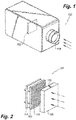
- FIG. 1 a partial view of an exemplary embodiment of an imaging camera system in accordance with the disclosure is shown in Fig. 1 and is designated generally by reference character 100.
- the systems and methods described herein can be used for infrared detection and imaging that excludes predetermined wavelengths.
- An imaging camera system 100 includes a sensor 102 that includes an InGaAs photodetector configured to convert received infrared radiation, indicated by the triple arrows in Figs. 1-2 , into electrical signals.
- the InGaAs photodetector includes a two-dimensional array of photodetector pixels, indicated by the grid texture on sensor 102 in Fig. 2 . Each pixel is configured to convert infrared radiation into electrical signals for imaging.
- At least one optical lens element 106 is optically coupled to the InGaAs photodetector to focus an image on the array, so the sensor 102 functions as a focal plane array (FPA), however embodiments including only a single photodetector, a one-dimensional array of photodetector pixels, or any other suitable configuration are all contemplated within the scope of this disclosure.
- a notch filter 108 is operatively connected to the InGaAs photodetector of sensor 102 to block detection of wavelengths within each of three respective, non-overlapping bands, one band including 850nm, one band including 1060nm, and one band including 1550nm.
- a Read-Out Integrated Circuit (ROIC) 104 is operatively connected to the array of sensor 102 to condition electrical signals from the array for imaging.
- ROIC Read-Out Integrated Circuit
- the notch filter 108 includes an optical coating directly on a surface of the InGaAs photodetector of sensor 102, as indicated by the dashed lines in Fig. 2 associated with reference character 108.
- the optical coating can be monolithic with the InGaAs photodetector, and can be applied to the InGaAs detector by any suitable film deposition technique, e.g., for high volume commercial semiconductor processing. It is also contemplated in addition to or in lieu of notch filter 108, that the notch filter can be securely embedded in an optical path of the InGaAs photodetector, e.g., spaced apart from the InGaAs photodetector such as indicated in Fig. 2 with the broken line associated with reference character 110.
- a single notch filter can be used, or multiple notch filters, each for blocking a respective bandwidth or bandwidths, can be used at any suitable position in the optical path of system 100 leading to sensor 102.
- a filter assembly e.g., included in the notch filter 108/110 or separate therefrom, can be optically coupled to the InGaAs photodetector to improve signal to noise ratio.
- the InGaAs photodetector of sensor 102 can be configured to receive wavelengths up to and including 1700 nm.
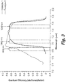
- quantum efficiency curves are shown for two exemplary InGaAs photodetectors, each having a cutoff at or around 1700 nm.
- the sensor 102 for Example 1 has a higher quantum efficiency for visible light than the sensor 102 for Example 2, however in both examples the InGaAs photodetector is sensitive to at least one of SWIR (e.g. wavelengths from 1.4-3.0 ⁇ m) or NIR (e.g., wavelengths from 0.75-1.4 ⁇ m) radiation outside the at least one predetermined bands of notch filter 108/110.
- SWIR e.g. wavelengths from 1.4-3.0 ⁇ m
- NIR e.g., wavelengths from 0.75-1.4 ⁇ m
- the notch filter 108/110 is configured to block detection of wavelengths within predetermined bands including 850 nm, 1060 nm, and/or 1550 nm.
- the notch filter 108/110 for each of these two examples is configured to reflect or block detection of wavelengths within each of three respective, non-overlapping bands, one band including 850 nm ⁇ 20 nm, one band including 1060 nm ⁇ 20 nm, and one band including 1550 nm ⁇ 20 nm, as indicated in Fig. 3 by the rectangles.
- the 40 nm notch width in these examples can vary without departing from the scope of this disclosure, as can the centers of the notch bandwidth, as can the number of notches, as needed on an application by application basis.
- Eliminating detection of radiation in the notches of notch filter 108/110 allows for use in applications where it is desired to detect radiation across various portions of the spectrum of sensitivity for the InGaAs photodetector, wherein it is also desirable to prevent detection of radiation in the notch bands of notch filter 108/110, such as radiation from specific laser sources centered around the 860, 1060, and 1550 nm wavelengths. For example, there are applications which can benefit from ensuring that such laser sources do not interfere with the two-dimensional imagery obtained from an infrared sensor.
Landscapes
- Physics & Mathematics (AREA)
- General Physics & Mathematics (AREA)
- Spectroscopy & Molecular Physics (AREA)
- Photometry And Measurement Of Optical Pulse Characteristics (AREA)
- Light Receiving Elements (AREA)
- Solid State Image Pick-Up Elements (AREA)
- Transforming Light Signals Into Electric Signals (AREA)
Claims (11)
- Sensor, umfassend:einen InGaAs-Photodetektor (102), der so konfiguriert ist, dass er empfangene Infrarotstrahlung in elektrische Signale umwandelt; undeinen Kerbfilter (108, 110), der wirksam mit dem InGaAs-Photodetektor verbunden ist, dadurch gekennzeichnet, dass der Kerbfilter so konfiguriert ist, dass er die Erkennung von Wellenlängen innerhalb jeder von drei jeweiligen, nicht überlappenden Banden blockiert, wobei eine Bande 850 nm beinhaltet, eine Bande 1060 nm beinhaltet und eine Bande 1550 nm beinhaltet.
- Sensor nach Anspruch 1, wobei der InGaAs-Photodetektor auf mindestens eine aus SWIR- oder NIR-Strahlung außerhalb der mindestens einen vorbestimmten Bande empfindlich reagiert.
- Sensor nach einem der vorstehenden Ansprüche, ferner einen ROIC (104) umfassend, der wirksam mit dem InGaAs-Photodetektor verbunden ist, um elektrische Signale von dem InGaAs-Photodetektor aufzubereiten.
- Sensor nach einem der vorstehenden Ansprüche, wobei der InGaAs-Photodetektor so konfiguriert ist, dass er Wellenlängen bis zu und einschließlich etwa 1700 nm empfängt.
- Sensor nach einem der vorstehenden Ansprüche, ferner eine Filteranordnung umfassend, die optisch an den InGaAs-Photodetektor gekoppelt ist, um das Signal-Rausch-Verhältnis zu verbessern.
- Sensor nach einem der vorstehenden Ansprüche, wobei der Kerbfilter eine optische Beschichtung direkt an einer Fläche des InGaAs-Photodetektors aufweist.
- Sensor nach Anspruch 6, wobei die optische Beschichtung mit dem InGaAs-Photodetektor monolithisch ist.
- Sensor nach einem der vorstehenden Ansprüche, wobei der Kerbfilter in einem Strahlengang des InGaAs-Photodetektors fest eingebettet ist.
- Sensor nach einem der vorstehenden Ansprüche, wobei der InGaAs-Photodetektor eine zweidimensionale Anordnung von Photodetektor-Pixeln beinhaltet, die jeweils so konfiguriert sind, dass sie eine Infrarotstrahlung in elektrische Signale für die Bildgebung umwandeln.
- Sensor nach Anspruch 9, ferner einen ROIC umfassend, der wirksam mit der zweidimensionalen Anordnung von Photodetektor-Pixeln verbunden ist, um elektrische Signale von der zweidimensionalen Anordnung für die Bildgebung aufzubereiten.
- Bildkamerasystem (100), Folgendes umfassend:einen InGaAs-Photodetektor (102), der so konfiguriert ist, dass er empfangene Infrarotstrahlung in elektrische Signale umwandelt, wobei der InGaAs-Photodetektor eine Anordnung von Photodetektor-Pixeln beinhaltet, die jeweils so konfiguriert sind, dass sie Infrarotstrahlung in elektrische Signale für die Bildgebung umwandeln;mindestens ein optisches Element (106), das optisch an den InGaAs-Photodetektor gekoppelt ist, um ein Bild auf der Anordnung zu fokussieren;einen Kerbfilter (108), der wirksam mit dem InGaAs-Photodetektor verbunden ist; undeinen ROIC (104), der wirksam mit der Anordnung verbunden ist, um elektrische Signale von der Anordnung für die Bildgebung aufzuarbeiten;dadurch gekennzeichnet, dass der Kerbfilter so konfiguriert ist, dass er die Erkennung von Wellenlängen innerhalb jeder von drei jeweiligen, nicht überlappenden Banden blockiert, wobei eine Bande 850 nm beinhaltet, eine Bande 1060 nm beinhaltet und eine Bande 1550 nm beinhaltet.
Applications Claiming Priority (1)
| Application Number | Priority Date | Filing Date | Title |
|---|---|---|---|
| US201562246512P | 2015-10-26 | 2015-10-26 |
Publications (2)
| Publication Number | Publication Date |
|---|---|
| EP3166151A1 EP3166151A1 (de) | 2017-05-10 |
| EP3166151B1 true EP3166151B1 (de) | 2021-05-19 |
Family
ID=57208163
Family Applications (1)
| Application Number | Title | Priority Date | Filing Date |
|---|---|---|---|
| EP16195743.6A Active EP3166151B1 (de) | 2015-10-26 | 2016-10-26 | Infrarot-bildebenenarray mit eingeschränkter quanteneffizienz |
Country Status (3)
| Country | Link |
|---|---|
| US (1) | US9842868B2 (de) |
| EP (1) | EP3166151B1 (de) |
| JP (1) | JP6739311B2 (de) |
Families Citing this family (3)
| Publication number | Priority date | Publication date | Assignee | Title |
|---|---|---|---|---|
| KR102547801B1 (ko) | 2017-08-28 | 2023-06-26 | 삼성전자주식회사 | 적외선 검출기 및 이를 포함하는 적외선 센서 |
| JP7137925B2 (ja) * | 2017-12-08 | 2022-09-15 | 株式会社 堀場アドバンスドテクノ | 放射温度計 |
| GB2589065B (en) * | 2019-10-23 | 2024-08-21 | Smart Photonics Holding B V | Fabricating a semiconductor structure with multiple quantum wells |
Family Cites Families (23)
| Publication number | Priority date | Publication date | Assignee | Title |
|---|---|---|---|---|
| AU2001272003A1 (en) * | 2000-07-13 | 2002-02-05 | Virginia Commonwealth University | Use of ultraviolet, near-ultraviolet and near infrared resonance raman spectroscopy and fluorescence spectroscopy for tissue interrogation of shock states, critical illnesses, and other disease states |
| WO2004061127A2 (en) | 2003-01-02 | 2004-07-22 | University Of Rochester | Hybridization-based biosensor containing hairpin probes and use thereof |
| US7496293B2 (en) * | 2004-01-14 | 2009-02-24 | Elbit Systems Ltd. | Versatile camera for various visibility conditions |
| US7652765B1 (en) | 2004-03-06 | 2010-01-26 | Plain Sight Systems, Inc. | Hyper-spectral imaging methods and devices |
| US7394542B2 (en) | 2004-08-18 | 2008-07-01 | Chemimage Corporation | Method and apparatus for chemical imaging in a microfluidic circuit |
| EP2007132B1 (de) * | 2006-03-28 | 2013-05-08 | Kyocera Corporation | Nachtsichteinrichtung |
| US9354370B1 (en) * | 2007-09-25 | 2016-05-31 | Semrock, Inc. | Optical thin-film notch filter with very wide pass band regions |
| US8084739B2 (en) | 2008-07-16 | 2011-12-27 | Infrared Newco., Inc. | Imaging apparatus and methods |
| JP2011075441A (ja) * | 2009-09-30 | 2011-04-14 | Hamamatsu Photonics Kk | 半導体デバイス故障解析装置 |
| JP5692988B2 (ja) * | 2009-10-19 | 2015-04-01 | キヤノン株式会社 | 音響波測定装置 |
| US8619143B2 (en) * | 2010-03-19 | 2013-12-31 | Pixim, Inc. | Image sensor including color and infrared pixels |
| WO2011127247A2 (en) * | 2010-04-07 | 2011-10-13 | Sanjay Krishna | Apparatus and techniques of non-invasive analysis |
| US8744782B2 (en) | 2010-11-16 | 2014-06-03 | Corning Incorporated | System and method for simultaneously determining strain and temperature characteristics of an object |
| GB201104475D0 (en) | 2011-03-16 | 2011-04-27 | Filtrona Filter Prod Dev Co | Tobacco smoke filter |
| EP2766792A4 (de) * | 2011-10-10 | 2016-03-30 | Invisage Technologies Inc | Erfassung von ereignissen raum und zeit |
| US9171196B2 (en) * | 2012-03-09 | 2015-10-27 | Xerox Corporation | Multi-band infrared camera system optimized for skin detection |
| US9163905B2 (en) * | 2012-05-23 | 2015-10-20 | Rosemount Aerospace Inc. | Dual-mode SAL/IR imaging |
| CN105308626A (zh) * | 2013-01-17 | 2016-02-03 | 西奥尼克斯股份有限公司 | 生物识别成像装置以及其方法 |
| US9111830B1 (en) * | 2013-05-22 | 2015-08-18 | Sensors Unlimited, Inc. | Perforated blocking layer for enhanced broad band response in a focal plane array |
| KR102071325B1 (ko) * | 2013-09-27 | 2020-04-02 | 매그나칩 반도체 유한회사 | 조도와 물체의 거리를 측정하는 광 센서 |
| CN107193126B (zh) * | 2013-11-27 | 2020-06-05 | 奇跃公司 | 虚拟和增强现实系统与方法 |
| US9485439B2 (en) * | 2013-12-03 | 2016-11-01 | Sensors Unlimited, Inc. | Shortwave infrared camera with bandwidth restriction |
| US10209362B2 (en) * | 2015-03-27 | 2019-02-19 | Sensors Unlimited, Inc. | Detecting, tracking, and decoding pulse repetition frequency laser energy from laser designators |
-
2016
- 2016-02-04 US US15/016,015 patent/US9842868B2/en active Active
- 2016-10-25 JP JP2016208466A patent/JP6739311B2/ja active Active
- 2016-10-26 EP EP16195743.6A patent/EP3166151B1/de active Active
Non-Patent Citations (1)
| Title |
|---|
| None * |
Also Published As
| Publication number | Publication date |
|---|---|
| US20170117308A1 (en) | 2017-04-27 |
| JP2017083443A (ja) | 2017-05-18 |
| US9842868B2 (en) | 2017-12-12 |
| EP3166151A1 (de) | 2017-05-10 |
| JP6739311B2 (ja) | 2020-08-12 |
Similar Documents
| Publication | Publication Date | Title |
|---|---|---|
| US20100051809A1 (en) | Monolithic Dual Band Imager | |
| US8378300B2 (en) | Near-infrared imaging sensor | |
| US8415608B2 (en) | Frequency selective communications system | |
| Rutz et al. | InGaAs SWIR photodetectors for night vision | |
| JP2008205001A (ja) | 受光素子、センサおよび撮像装置 | |
| Rouvié et al. | SWIR InGaAs focal plane arrays in France | |
| US6580089B2 (en) | Multi-quantum-well infrared sensor array in spatially-separated multi-band configuration | |
| US9842868B2 (en) | Quantum efficiency (QE) restricted infrared focal plane arrays | |
| Goldberg et al. | Comparison of HgCdTe and quantum-well infrared photodetector dual-band focal plane arrays | |
| Mohammadnejad et al. | Analysis of structures and technologies of various types of photodetectors used in laser warning systems: a review | |
| JP5991036B2 (ja) | 受光素子および光学装置 | |
| Rothman et al. | HgCdTe APDs for low photon number IR detection | |
| Daumer et al. | Photodetector development at Fraunhofer IAF: From LWIR to SWIR operating from cryogenic close to room temperature | |
| Rothman et al. | HgCdTe APDs for free space optical communications | |
| Rutz et al. | SWIR detectors for low photon fluxes | |
| Martin et al. | 320x240 pixel InGaAs/InP focal plane array for short-wave infrared and visible light imaging | |
| MacDougal et al. | Short-wavelength infrared imaging using low dark current InGaAs detector arrays and vertical-cavity surface-emitting laser illuminators | |
| Rutz et al. | SWIR photodetector development at Fraunhofer IAF | |
| Rutz et al. | Low-light-level SWIR photodetectors based on the InGaAs material system | |
| Colin et al. | Development and integration of new functions in InGaAs imaging | |
| Gunapala et al. | Type-II strained-layer superlattice digital focal plane arrays for earth remote sensing instruments | |
| Eckardt et al. | CMOS-TDI detector technology for reconnaissance application | |
| WO2014002082A2 (en) | Photodetector device | |
| KR102220277B1 (ko) | 대역폭 제한을 가진 단파 적외선 카메라 | |
| US7936528B2 (en) | Graded order-sorting filter for hyperspectral imagers and methods of making the same |
Legal Events
| Date | Code | Title | Description |
|---|---|---|---|
| PUAI | Public reference made under article 153(3) epc to a published international application that has entered the european phase |
Free format text: ORIGINAL CODE: 0009012 |
|
| STAA | Information on the status of an ep patent application or granted ep patent |
Free format text: STATUS: THE APPLICATION HAS BEEN PUBLISHED |
|
| AK | Designated contracting states |
Kind code of ref document: A1 Designated state(s): AL AT BE BG CH CY CZ DE DK EE ES FI FR GB GR HR HU IE IS IT LI LT LU LV MC MK MT NL NO PL PT RO RS SE SI SK SM TR |
|
| AX | Request for extension of the european patent |
Extension state: BA ME |
|
| STAA | Information on the status of an ep patent application or granted ep patent |
Free format text: STATUS: REQUEST FOR EXAMINATION WAS MADE |
|
| 17P | Request for examination filed |
Effective date: 20171110 |
|
| RBV | Designated contracting states (corrected) |
Designated state(s): AL AT BE BG CH CY CZ DE DK EE ES FI FR GB GR HR HU IE IS IT LI LT LU LV MC MK MT NL NO PL PT RO RS SE SI SK SM TR |
|
| GRAP | Despatch of communication of intention to grant a patent |
Free format text: ORIGINAL CODE: EPIDOSNIGR1 |
|
| STAA | Information on the status of an ep patent application or granted ep patent |
Free format text: STATUS: GRANT OF PATENT IS INTENDED |
|
| INTG | Intention to grant announced |
Effective date: 20201207 |
|
| RIN1 | Information on inventor provided before grant (corrected) |
Inventor name: ROZPLOCH, ROBERT |
|
| GRAS | Grant fee paid |
Free format text: ORIGINAL CODE: EPIDOSNIGR3 |
|
| GRAA | (expected) grant |
Free format text: ORIGINAL CODE: 0009210 |
|
| STAA | Information on the status of an ep patent application or granted ep patent |
Free format text: STATUS: THE PATENT HAS BEEN GRANTED |
|
| AK | Designated contracting states |
Kind code of ref document: B1 Designated state(s): AL AT BE BG CH CY CZ DE DK EE ES FI FR GB GR HR HU IE IS IT LI LT LU LV MC MK MT NL NO PL PT RO RS SE SI SK SM TR |
|
| REG | Reference to a national code |
Ref country code: GB Ref legal event code: FG4D |
|
| REG | Reference to a national code |
Ref country code: CH Ref legal event code: EP |
|
| REG | Reference to a national code |
Ref country code: DE Ref legal event code: R096 Ref document number: 602016057968 Country of ref document: DE |
|
| REG | Reference to a national code |
Ref country code: AT Ref legal event code: REF Ref document number: 1394839 Country of ref document: AT Kind code of ref document: T Effective date: 20210615 |
|
| REG | Reference to a national code |
Ref country code: IE Ref legal event code: FG4D |
|
| REG | Reference to a national code |
Ref country code: LT Ref legal event code: MG9D |
|
| REG | Reference to a national code |
Ref country code: AT Ref legal event code: MK05 Ref document number: 1394839 Country of ref document: AT Kind code of ref document: T Effective date: 20210519 |
|
| REG | Reference to a national code |
Ref country code: NL Ref legal event code: MP Effective date: 20210519 |
|
| PG25 | Lapsed in a contracting state [announced via postgrant information from national office to epo] |
Ref country code: LT Free format text: LAPSE BECAUSE OF FAILURE TO SUBMIT A TRANSLATION OF THE DESCRIPTION OR TO PAY THE FEE WITHIN THE PRESCRIBED TIME-LIMIT Effective date: 20210519 Ref country code: FI Free format text: LAPSE BECAUSE OF FAILURE TO SUBMIT A TRANSLATION OF THE DESCRIPTION OR TO PAY THE FEE WITHIN THE PRESCRIBED TIME-LIMIT Effective date: 20210519 Ref country code: HR Free format text: LAPSE BECAUSE OF FAILURE TO SUBMIT A TRANSLATION OF THE DESCRIPTION OR TO PAY THE FEE WITHIN THE PRESCRIBED TIME-LIMIT Effective date: 20210519 Ref country code: AT Free format text: LAPSE BECAUSE OF FAILURE TO SUBMIT A TRANSLATION OF THE DESCRIPTION OR TO PAY THE FEE WITHIN THE PRESCRIBED TIME-LIMIT Effective date: 20210519 Ref country code: BG Free format text: LAPSE BECAUSE OF FAILURE TO SUBMIT A TRANSLATION OF THE DESCRIPTION OR TO PAY THE FEE WITHIN THE PRESCRIBED TIME-LIMIT Effective date: 20210819 |
|
| PG25 | Lapsed in a contracting state [announced via postgrant information from national office to epo] |
Ref country code: IS Free format text: LAPSE BECAUSE OF FAILURE TO SUBMIT A TRANSLATION OF THE DESCRIPTION OR TO PAY THE FEE WITHIN THE PRESCRIBED TIME-LIMIT Effective date: 20210919 Ref country code: LV Free format text: LAPSE BECAUSE OF FAILURE TO SUBMIT A TRANSLATION OF THE DESCRIPTION OR TO PAY THE FEE WITHIN THE PRESCRIBED TIME-LIMIT Effective date: 20210519 Ref country code: GR Free format text: LAPSE BECAUSE OF FAILURE TO SUBMIT A TRANSLATION OF THE DESCRIPTION OR TO PAY THE FEE WITHIN THE PRESCRIBED TIME-LIMIT Effective date: 20210820 Ref country code: ES Free format text: LAPSE BECAUSE OF FAILURE TO SUBMIT A TRANSLATION OF THE DESCRIPTION OR TO PAY THE FEE WITHIN THE PRESCRIBED TIME-LIMIT Effective date: 20210519 Ref country code: NO Free format text: LAPSE BECAUSE OF FAILURE TO SUBMIT A TRANSLATION OF THE DESCRIPTION OR TO PAY THE FEE WITHIN THE PRESCRIBED TIME-LIMIT Effective date: 20210819 Ref country code: PL Free format text: LAPSE BECAUSE OF FAILURE TO SUBMIT A TRANSLATION OF THE DESCRIPTION OR TO PAY THE FEE WITHIN THE PRESCRIBED TIME-LIMIT Effective date: 20210519 Ref country code: PT Free format text: LAPSE BECAUSE OF FAILURE TO SUBMIT A TRANSLATION OF THE DESCRIPTION OR TO PAY THE FEE WITHIN THE PRESCRIBED TIME-LIMIT Effective date: 20210920 Ref country code: RS Free format text: LAPSE BECAUSE OF FAILURE TO SUBMIT A TRANSLATION OF THE DESCRIPTION OR TO PAY THE FEE WITHIN THE PRESCRIBED TIME-LIMIT Effective date: 20210519 Ref country code: SE Free format text: LAPSE BECAUSE OF FAILURE TO SUBMIT A TRANSLATION OF THE DESCRIPTION OR TO PAY THE FEE WITHIN THE PRESCRIBED TIME-LIMIT Effective date: 20210519 |
|
| PG25 | Lapsed in a contracting state [announced via postgrant information from national office to epo] |
Ref country code: NL Free format text: LAPSE BECAUSE OF FAILURE TO SUBMIT A TRANSLATION OF THE DESCRIPTION OR TO PAY THE FEE WITHIN THE PRESCRIBED TIME-LIMIT Effective date: 20210519 |
|
| PG25 | Lapsed in a contracting state [announced via postgrant information from national office to epo] |
Ref country code: RO Free format text: LAPSE BECAUSE OF FAILURE TO SUBMIT A TRANSLATION OF THE DESCRIPTION OR TO PAY THE FEE WITHIN THE PRESCRIBED TIME-LIMIT Effective date: 20210519 Ref country code: SK Free format text: LAPSE BECAUSE OF FAILURE TO SUBMIT A TRANSLATION OF THE DESCRIPTION OR TO PAY THE FEE WITHIN THE PRESCRIBED TIME-LIMIT Effective date: 20210519 Ref country code: SM Free format text: LAPSE BECAUSE OF FAILURE TO SUBMIT A TRANSLATION OF THE DESCRIPTION OR TO PAY THE FEE WITHIN THE PRESCRIBED TIME-LIMIT Effective date: 20210519 Ref country code: EE Free format text: LAPSE BECAUSE OF FAILURE TO SUBMIT A TRANSLATION OF THE DESCRIPTION OR TO PAY THE FEE WITHIN THE PRESCRIBED TIME-LIMIT Effective date: 20210519 Ref country code: CZ Free format text: LAPSE BECAUSE OF FAILURE TO SUBMIT A TRANSLATION OF THE DESCRIPTION OR TO PAY THE FEE WITHIN THE PRESCRIBED TIME-LIMIT Effective date: 20210519 Ref country code: DK Free format text: LAPSE BECAUSE OF FAILURE TO SUBMIT A TRANSLATION OF THE DESCRIPTION OR TO PAY THE FEE WITHIN THE PRESCRIBED TIME-LIMIT Effective date: 20210519 |
|
| REG | Reference to a national code |
Ref country code: DE Ref legal event code: R097 Ref document number: 602016057968 Country of ref document: DE |
|
| PLBE | No opposition filed within time limit |
Free format text: ORIGINAL CODE: 0009261 |
|
| STAA | Information on the status of an ep patent application or granted ep patent |
Free format text: STATUS: NO OPPOSITION FILED WITHIN TIME LIMIT |
|
| 26N | No opposition filed |
Effective date: 20220222 |
|
| PG25 | Lapsed in a contracting state [announced via postgrant information from national office to epo] |
Ref country code: IS Free format text: LAPSE BECAUSE OF FAILURE TO SUBMIT A TRANSLATION OF THE DESCRIPTION OR TO PAY THE FEE WITHIN THE PRESCRIBED TIME-LIMIT Effective date: 20210919 Ref country code: AL Free format text: LAPSE BECAUSE OF FAILURE TO SUBMIT A TRANSLATION OF THE DESCRIPTION OR TO PAY THE FEE WITHIN THE PRESCRIBED TIME-LIMIT Effective date: 20210519 |
|
| REG | Reference to a national code |
Ref country code: CH Ref legal event code: PL |
|
| REG | Reference to a national code |
Ref country code: BE Ref legal event code: MM Effective date: 20211031 |
|
| GBPC | Gb: european patent ceased through non-payment of renewal fee |
Effective date: 20211026 |
|
| PG25 | Lapsed in a contracting state [announced via postgrant information from national office to epo] |
Ref country code: MC Free format text: LAPSE BECAUSE OF FAILURE TO SUBMIT A TRANSLATION OF THE DESCRIPTION OR TO PAY THE FEE WITHIN THE PRESCRIBED TIME-LIMIT Effective date: 20210519 |
|
| PG25 | Lapsed in a contracting state [announced via postgrant information from national office to epo] |
Ref country code: LU Free format text: LAPSE BECAUSE OF NON-PAYMENT OF DUE FEES Effective date: 20211026 Ref country code: IT Free format text: LAPSE BECAUSE OF FAILURE TO SUBMIT A TRANSLATION OF THE DESCRIPTION OR TO PAY THE FEE WITHIN THE PRESCRIBED TIME-LIMIT Effective date: 20210519 Ref country code: GB Free format text: LAPSE BECAUSE OF NON-PAYMENT OF DUE FEES Effective date: 20211026 Ref country code: BE Free format text: LAPSE BECAUSE OF NON-PAYMENT OF DUE FEES Effective date: 20211031 |
|
| PG25 | Lapsed in a contracting state [announced via postgrant information from national office to epo] |
Ref country code: LI Free format text: LAPSE BECAUSE OF NON-PAYMENT OF DUE FEES Effective date: 20211031 Ref country code: CH Free format text: LAPSE BECAUSE OF NON-PAYMENT OF DUE FEES Effective date: 20211031 |
|
| PG25 | Lapsed in a contracting state [announced via postgrant information from national office to epo] |
Ref country code: FR Free format text: LAPSE BECAUSE OF NON-PAYMENT OF DUE FEES Effective date: 20211031 |
|
| PG25 | Lapsed in a contracting state [announced via postgrant information from national office to epo] |
Ref country code: IE Free format text: LAPSE BECAUSE OF NON-PAYMENT OF DUE FEES Effective date: 20211026 |
|
| PG25 | Lapsed in a contracting state [announced via postgrant information from national office to epo] |
Ref country code: HU Free format text: LAPSE BECAUSE OF FAILURE TO SUBMIT A TRANSLATION OF THE DESCRIPTION OR TO PAY THE FEE WITHIN THE PRESCRIBED TIME-LIMIT; INVALID AB INITIO Effective date: 20161026 |
|
| PG25 | Lapsed in a contracting state [announced via postgrant information from national office to epo] |
Ref country code: CY Free format text: LAPSE BECAUSE OF FAILURE TO SUBMIT A TRANSLATION OF THE DESCRIPTION OR TO PAY THE FEE WITHIN THE PRESCRIBED TIME-LIMIT Effective date: 20210519 |
|
| PG25 | Lapsed in a contracting state [announced via postgrant information from national office to epo] |
Ref country code: MK Free format text: LAPSE BECAUSE OF FAILURE TO SUBMIT A TRANSLATION OF THE DESCRIPTION OR TO PAY THE FEE WITHIN THE PRESCRIBED TIME-LIMIT Effective date: 20210519 |
|
| PG25 | Lapsed in a contracting state [announced via postgrant information from national office to epo] |
Ref country code: MT Free format text: LAPSE BECAUSE OF FAILURE TO SUBMIT A TRANSLATION OF THE DESCRIPTION OR TO PAY THE FEE WITHIN THE PRESCRIBED TIME-LIMIT Effective date: 20210519 |
|
| REG | Reference to a national code |
Ref country code: DE Ref legal event code: R079 Ref document number: 602016057968 Country of ref document: DE Free format text: PREVIOUS MAIN CLASS: H01L0031021600 Ipc: H10F0077300000 |
|
| PG25 | Lapsed in a contracting state [announced via postgrant information from national office to epo] |
Ref country code: TR Free format text: LAPSE BECAUSE OF FAILURE TO SUBMIT A TRANSLATION OF THE DESCRIPTION OR TO PAY THE FEE WITHIN THE PRESCRIBED TIME-LIMIT Effective date: 20210519 |
|
| PGFP | Annual fee paid to national office [announced via postgrant information from national office to epo] |
Ref country code: DE Payment date: 20250923 Year of fee payment: 10 |
|
| P01 | Opt-out of the competence of the unified patent court (upc) registered |
Free format text: CASE NUMBER: UPC_APP_0016818_3166151/2025 Effective date: 20251210 |