EP3165361A1 - Polymer conductor sheets, solar cells and methods for producing same - Google Patents
Polymer conductor sheets, solar cells and methods for producing same Download PDFInfo
- Publication number
- EP3165361A1 EP3165361A1 EP15193339.7A EP15193339A EP3165361A1 EP 3165361 A1 EP3165361 A1 EP 3165361A1 EP 15193339 A EP15193339 A EP 15193339A EP 3165361 A1 EP3165361 A1 EP 3165361A1
- Authority
- EP
- European Patent Office
- Prior art keywords
- zone
- sheet
- polymer
- conductor
- polymer conductor
- Prior art date
- Legal status (The legal status is an assumption and is not a legal conclusion. Google has not performed a legal analysis and makes no representation as to the accuracy of the status listed.)
- Granted
Links
Images


Classifications
-
- H—ELECTRICITY
- H10—SEMICONDUCTOR DEVICES; ELECTRIC SOLID-STATE DEVICES NOT OTHERWISE PROVIDED FOR
- H10F—INORGANIC SEMICONDUCTOR DEVICES SENSITIVE TO INFRARED RADIATION, LIGHT, ELECTROMAGNETIC RADIATION OF SHORTER WAVELENGTH OR CORPUSCULAR RADIATION
- H10F19/00—Integrated devices, or assemblies of multiple devices, comprising at least one photovoltaic cell covered by group H10F10/00, e.g. photovoltaic modules
- H10F19/90—Structures for connecting between photovoltaic cells, e.g. interconnections or insulating spacers
- H10F19/902—Structures for connecting between photovoltaic cells, e.g. interconnections or insulating spacers for series or parallel connection of photovoltaic cells
- H10F19/906—Structures for connecting between photovoltaic cells, e.g. interconnections or insulating spacers for series or parallel connection of photovoltaic cells characterised by the materials of the structures
-
- B—PERFORMING OPERATIONS; TRANSPORTING
- B32—LAYERED PRODUCTS
- B32B—LAYERED PRODUCTS, i.e. PRODUCTS BUILT-UP OF STRATA OF FLAT OR NON-FLAT, e.g. CELLULAR OR HONEYCOMB, FORM
- B32B17/00—Layered products essentially comprising sheet glass, or glass, slag, or like fibres
-
- B—PERFORMING OPERATIONS; TRANSPORTING
- B32—LAYERED PRODUCTS
- B32B—LAYERED PRODUCTS, i.e. PRODUCTS BUILT-UP OF STRATA OF FLAT OR NON-FLAT, e.g. CELLULAR OR HONEYCOMB, FORM
- B32B17/00—Layered products essentially comprising sheet glass, or glass, slag, or like fibres
- B32B17/06—Layered products essentially comprising sheet glass, or glass, slag, or like fibres comprising glass as the main or only constituent of a layer, next to another layer of a specific material
- B32B17/10—Layered products essentially comprising sheet glass, or glass, slag, or like fibres comprising glass as the main or only constituent of a layer, next to another layer of a specific material of synthetic resin
-
- B—PERFORMING OPERATIONS; TRANSPORTING
- B32—LAYERED PRODUCTS
- B32B—LAYERED PRODUCTS, i.e. PRODUCTS BUILT-UP OF STRATA OF FLAT OR NON-FLAT, e.g. CELLULAR OR HONEYCOMB, FORM
- B32B25/00—Layered products comprising a layer of natural or synthetic rubber
- B32B25/04—Layered products comprising a layer of natural or synthetic rubber comprising rubber as the main or only constituent of a layer, which is next to another layer of the same or of a different material
-
- B—PERFORMING OPERATIONS; TRANSPORTING
- B32—LAYERED PRODUCTS
- B32B—LAYERED PRODUCTS, i.e. PRODUCTS BUILT-UP OF STRATA OF FLAT OR NON-FLAT, e.g. CELLULAR OR HONEYCOMB, FORM
- B32B25/00—Layered products comprising a layer of natural or synthetic rubber
- B32B25/04—Layered products comprising a layer of natural or synthetic rubber comprising rubber as the main or only constituent of a layer, which is next to another layer of the same or of a different material
- B32B25/042—Layered products comprising a layer of natural or synthetic rubber comprising rubber as the main or only constituent of a layer, which is next to another layer of the same or of a different material of natural rubber or synthetic rubber
-
- B—PERFORMING OPERATIONS; TRANSPORTING
- B32—LAYERED PRODUCTS
- B32B—LAYERED PRODUCTS, i.e. PRODUCTS BUILT-UP OF STRATA OF FLAT OR NON-FLAT, e.g. CELLULAR OR HONEYCOMB, FORM
- B32B25/00—Layered products comprising a layer of natural or synthetic rubber
- B32B25/14—Layered products comprising a layer of natural or synthetic rubber comprising synthetic rubber copolymers
-
- B—PERFORMING OPERATIONS; TRANSPORTING
- B32—LAYERED PRODUCTS
- B32B—LAYERED PRODUCTS, i.e. PRODUCTS BUILT-UP OF STRATA OF FLAT OR NON-FLAT, e.g. CELLULAR OR HONEYCOMB, FORM
- B32B27/00—Layered products comprising a layer of synthetic resin
- B32B27/06—Layered products comprising a layer of synthetic resin as the main or only constituent of a layer, which is next to another layer of the same or of a different material
-
- B—PERFORMING OPERATIONS; TRANSPORTING
- B32—LAYERED PRODUCTS
- B32B—LAYERED PRODUCTS, i.e. PRODUCTS BUILT-UP OF STRATA OF FLAT OR NON-FLAT, e.g. CELLULAR OR HONEYCOMB, FORM
- B32B27/00—Layered products comprising a layer of synthetic resin
- B32B27/06—Layered products comprising a layer of synthetic resin as the main or only constituent of a layer, which is next to another layer of the same or of a different material
- B32B27/08—Layered products comprising a layer of synthetic resin as the main or only constituent of a layer, which is next to another layer of the same or of a different material of synthetic resin
-
- B—PERFORMING OPERATIONS; TRANSPORTING
- B32—LAYERED PRODUCTS
- B32B—LAYERED PRODUCTS, i.e. PRODUCTS BUILT-UP OF STRATA OF FLAT OR NON-FLAT, e.g. CELLULAR OR HONEYCOMB, FORM
- B32B27/00—Layered products comprising a layer of synthetic resin
- B32B27/16—Layered products comprising a layer of synthetic resin specially treated, e.g. irradiated
-
- B—PERFORMING OPERATIONS; TRANSPORTING
- B32—LAYERED PRODUCTS
- B32B—LAYERED PRODUCTS, i.e. PRODUCTS BUILT-UP OF STRATA OF FLAT OR NON-FLAT, e.g. CELLULAR OR HONEYCOMB, FORM
- B32B27/00—Layered products comprising a layer of synthetic resin
- B32B27/18—Layered products comprising a layer of synthetic resin characterised by the use of special additives
- B32B27/20—Layered products comprising a layer of synthetic resin characterised by the use of special additives using fillers, pigments, thixotroping agents
-
- B—PERFORMING OPERATIONS; TRANSPORTING
- B32—LAYERED PRODUCTS
- B32B—LAYERED PRODUCTS, i.e. PRODUCTS BUILT-UP OF STRATA OF FLAT OR NON-FLAT, e.g. CELLULAR OR HONEYCOMB, FORM
- B32B27/00—Layered products comprising a layer of synthetic resin
- B32B27/28—Layered products comprising a layer of synthetic resin comprising synthetic resins not wholly covered by any one of the sub-groups B32B27/30 - B32B27/42
- B32B27/281—Layered products comprising a layer of synthetic resin comprising synthetic resins not wholly covered by any one of the sub-groups B32B27/30 - B32B27/42 comprising polyimides
-
- B—PERFORMING OPERATIONS; TRANSPORTING
- B32—LAYERED PRODUCTS
- B32B—LAYERED PRODUCTS, i.e. PRODUCTS BUILT-UP OF STRATA OF FLAT OR NON-FLAT, e.g. CELLULAR OR HONEYCOMB, FORM
- B32B27/00—Layered products comprising a layer of synthetic resin
- B32B27/28—Layered products comprising a layer of synthetic resin comprising synthetic resins not wholly covered by any one of the sub-groups B32B27/30 - B32B27/42
- B32B27/283—Layered products comprising a layer of synthetic resin comprising synthetic resins not wholly covered by any one of the sub-groups B32B27/30 - B32B27/42 comprising polysiloxanes
-
- B—PERFORMING OPERATIONS; TRANSPORTING
- B32—LAYERED PRODUCTS
- B32B—LAYERED PRODUCTS, i.e. PRODUCTS BUILT-UP OF STRATA OF FLAT OR NON-FLAT, e.g. CELLULAR OR HONEYCOMB, FORM
- B32B27/00—Layered products comprising a layer of synthetic resin
- B32B27/30—Layered products comprising a layer of synthetic resin comprising vinyl (co)polymers; comprising acrylic (co)polymers
- B32B27/304—Layered products comprising a layer of synthetic resin comprising vinyl (co)polymers; comprising acrylic (co)polymers comprising vinyl halide (co)polymers, e.g. PVC, PVDC, PVF, PVDF
-
- B—PERFORMING OPERATIONS; TRANSPORTING
- B32—LAYERED PRODUCTS
- B32B—LAYERED PRODUCTS, i.e. PRODUCTS BUILT-UP OF STRATA OF FLAT OR NON-FLAT, e.g. CELLULAR OR HONEYCOMB, FORM
- B32B27/00—Layered products comprising a layer of synthetic resin
- B32B27/30—Layered products comprising a layer of synthetic resin comprising vinyl (co)polymers; comprising acrylic (co)polymers
- B32B27/306—Layered products comprising a layer of synthetic resin comprising vinyl (co)polymers; comprising acrylic (co)polymers comprising vinyl acetate or vinyl alcohol (co)polymers
-
- B—PERFORMING OPERATIONS; TRANSPORTING
- B32—LAYERED PRODUCTS
- B32B—LAYERED PRODUCTS, i.e. PRODUCTS BUILT-UP OF STRATA OF FLAT OR NON-FLAT, e.g. CELLULAR OR HONEYCOMB, FORM
- B32B27/00—Layered products comprising a layer of synthetic resin
- B32B27/30—Layered products comprising a layer of synthetic resin comprising vinyl (co)polymers; comprising acrylic (co)polymers
- B32B27/308—Layered products comprising a layer of synthetic resin comprising vinyl (co)polymers; comprising acrylic (co)polymers comprising acrylic (co)polymers
-
- B—PERFORMING OPERATIONS; TRANSPORTING
- B32—LAYERED PRODUCTS
- B32B—LAYERED PRODUCTS, i.e. PRODUCTS BUILT-UP OF STRATA OF FLAT OR NON-FLAT, e.g. CELLULAR OR HONEYCOMB, FORM
- B32B27/00—Layered products comprising a layer of synthetic resin
- B32B27/32—Layered products comprising a layer of synthetic resin comprising polyolefins
-
- B—PERFORMING OPERATIONS; TRANSPORTING
- B32—LAYERED PRODUCTS
- B32B—LAYERED PRODUCTS, i.e. PRODUCTS BUILT-UP OF STRATA OF FLAT OR NON-FLAT, e.g. CELLULAR OR HONEYCOMB, FORM
- B32B27/00—Layered products comprising a layer of synthetic resin
- B32B27/32—Layered products comprising a layer of synthetic resin comprising polyolefins
- B32B27/322—Layered products comprising a layer of synthetic resin comprising polyolefins comprising halogenated polyolefins, e.g. PTFE
-
- B—PERFORMING OPERATIONS; TRANSPORTING
- B32—LAYERED PRODUCTS
- B32B—LAYERED PRODUCTS, i.e. PRODUCTS BUILT-UP OF STRATA OF FLAT OR NON-FLAT, e.g. CELLULAR OR HONEYCOMB, FORM
- B32B27/00—Layered products comprising a layer of synthetic resin
- B32B27/34—Layered products comprising a layer of synthetic resin comprising polyamides
-
- B—PERFORMING OPERATIONS; TRANSPORTING
- B32—LAYERED PRODUCTS
- B32B—LAYERED PRODUCTS, i.e. PRODUCTS BUILT-UP OF STRATA OF FLAT OR NON-FLAT, e.g. CELLULAR OR HONEYCOMB, FORM
- B32B27/00—Layered products comprising a layer of synthetic resin
- B32B27/36—Layered products comprising a layer of synthetic resin comprising polyesters
-
- B—PERFORMING OPERATIONS; TRANSPORTING
- B32—LAYERED PRODUCTS
- B32B—LAYERED PRODUCTS, i.e. PRODUCTS BUILT-UP OF STRATA OF FLAT OR NON-FLAT, e.g. CELLULAR OR HONEYCOMB, FORM
- B32B27/00—Layered products comprising a layer of synthetic resin
- B32B27/40—Layered products comprising a layer of synthetic resin comprising polyurethanes
-
- B—PERFORMING OPERATIONS; TRANSPORTING
- B32—LAYERED PRODUCTS
- B32B—LAYERED PRODUCTS, i.e. PRODUCTS BUILT-UP OF STRATA OF FLAT OR NON-FLAT, e.g. CELLULAR OR HONEYCOMB, FORM
- B32B27/00—Layered products comprising a layer of synthetic resin
- B32B27/42—Layered products comprising a layer of synthetic resin comprising condensation resins of aldehydes, e.g. with phenols, ureas or melamines
-
- B—PERFORMING OPERATIONS; TRANSPORTING
- B32—LAYERED PRODUCTS
- B32B—LAYERED PRODUCTS, i.e. PRODUCTS BUILT-UP OF STRATA OF FLAT OR NON-FLAT, e.g. CELLULAR OR HONEYCOMB, FORM
- B32B3/00—Layered products comprising a layer with external or internal discontinuities or unevennesses, or a layer of non-planar shape; Layered products comprising a layer having particular features of form
- B32B3/02—Layered products comprising a layer with external or internal discontinuities or unevennesses, or a layer of non-planar shape; Layered products comprising a layer having particular features of form characterised by features of form at particular places, e.g. in edge regions
- B32B3/08—Layered products comprising a layer with external or internal discontinuities or unevennesses, or a layer of non-planar shape; Layered products comprising a layer having particular features of form characterised by features of form at particular places, e.g. in edge regions characterised by added members at particular parts
-
- B—PERFORMING OPERATIONS; TRANSPORTING
- B32—LAYERED PRODUCTS
- B32B—LAYERED PRODUCTS, i.e. PRODUCTS BUILT-UP OF STRATA OF FLAT OR NON-FLAT, e.g. CELLULAR OR HONEYCOMB, FORM
- B32B5/00—Layered products characterised by the non- homogeneity or physical structure, i.e. comprising a fibrous, filamentary, particulate or foam layer; Layered products characterised by having a layer differing constitutionally or physically in different parts
- B32B5/14—Layered products characterised by the non- homogeneity or physical structure, i.e. comprising a fibrous, filamentary, particulate or foam layer; Layered products characterised by having a layer differing constitutionally or physically in different parts characterised by a layer differing constitutionally or physically in different parts, e.g. denser near its faces
- B32B5/142—Variation across the area of the layer
-
- B—PERFORMING OPERATIONS; TRANSPORTING
- B32—LAYERED PRODUCTS
- B32B—LAYERED PRODUCTS, i.e. PRODUCTS BUILT-UP OF STRATA OF FLAT OR NON-FLAT, e.g. CELLULAR OR HONEYCOMB, FORM
- B32B5/00—Layered products characterised by the non- homogeneity or physical structure, i.e. comprising a fibrous, filamentary, particulate or foam layer; Layered products characterised by having a layer differing constitutionally or physically in different parts
- B32B5/14—Layered products characterised by the non- homogeneity or physical structure, i.e. comprising a fibrous, filamentary, particulate or foam layer; Layered products characterised by having a layer differing constitutionally or physically in different parts characterised by a layer differing constitutionally or physically in different parts, e.g. denser near its faces
- B32B5/147—Layered products characterised by the non- homogeneity or physical structure, i.e. comprising a fibrous, filamentary, particulate or foam layer; Layered products characterised by having a layer differing constitutionally or physically in different parts characterised by a layer differing constitutionally or physically in different parts, e.g. denser near its faces by treatment of the layer
-
- H—ELECTRICITY
- H10—SEMICONDUCTOR DEVICES; ELECTRIC SOLID-STATE DEVICES NOT OTHERWISE PROVIDED FOR
- H10F—INORGANIC SEMICONDUCTOR DEVICES SENSITIVE TO INFRARED RADIATION, LIGHT, ELECTROMAGNETIC RADIATION OF SHORTER WAVELENGTH OR CORPUSCULAR RADIATION
- H10F19/00—Integrated devices, or assemblies of multiple devices, comprising at least one photovoltaic cell covered by group H10F10/00, e.g. photovoltaic modules
- H10F19/80—Encapsulations or containers for integrated devices, or assemblies of multiple devices, having photovoltaic cells
-
- H—ELECTRICITY
- H10—SEMICONDUCTOR DEVICES; ELECTRIC SOLID-STATE DEVICES NOT OTHERWISE PROVIDED FOR
- H10F—INORGANIC SEMICONDUCTOR DEVICES SENSITIVE TO INFRARED RADIATION, LIGHT, ELECTROMAGNETIC RADIATION OF SHORTER WAVELENGTH OR CORPUSCULAR RADIATION
- H10F19/00—Integrated devices, or assemblies of multiple devices, comprising at least one photovoltaic cell covered by group H10F10/00, e.g. photovoltaic modules
- H10F19/80—Encapsulations or containers for integrated devices, or assemblies of multiple devices, having photovoltaic cells
- H10F19/807—Double-glass encapsulation, e.g. photovoltaic cells arranged between front and rear glass sheets
-
- B—PERFORMING OPERATIONS; TRANSPORTING
- B32—LAYERED PRODUCTS
- B32B—LAYERED PRODUCTS, i.e. PRODUCTS BUILT-UP OF STRATA OF FLAT OR NON-FLAT, e.g. CELLULAR OR HONEYCOMB, FORM
- B32B2255/00—Coating on the layer surface
- B32B2255/10—Coating on the layer surface on synthetic resin layer or on natural or synthetic rubber layer
-
- B—PERFORMING OPERATIONS; TRANSPORTING
- B32—LAYERED PRODUCTS
- B32B—LAYERED PRODUCTS, i.e. PRODUCTS BUILT-UP OF STRATA OF FLAT OR NON-FLAT, e.g. CELLULAR OR HONEYCOMB, FORM
- B32B2255/00—Coating on the layer surface
- B32B2255/20—Inorganic coating
- B32B2255/205—Metallic coating
-
- B—PERFORMING OPERATIONS; TRANSPORTING
- B32—LAYERED PRODUCTS
- B32B—LAYERED PRODUCTS, i.e. PRODUCTS BUILT-UP OF STRATA OF FLAT OR NON-FLAT, e.g. CELLULAR OR HONEYCOMB, FORM
- B32B2270/00—Resin or rubber layer containing a blend of at least two different polymers
-
- B—PERFORMING OPERATIONS; TRANSPORTING
- B32—LAYERED PRODUCTS
- B32B—LAYERED PRODUCTS, i.e. PRODUCTS BUILT-UP OF STRATA OF FLAT OR NON-FLAT, e.g. CELLULAR OR HONEYCOMB, FORM
- B32B2307/00—Properties of the layers or laminate
- B32B2307/20—Properties of the layers or laminate having particular electrical or magnetic properties, e.g. piezoelectric
- B32B2307/202—Conductive
-
- B—PERFORMING OPERATIONS; TRANSPORTING
- B32—LAYERED PRODUCTS
- B32B—LAYERED PRODUCTS, i.e. PRODUCTS BUILT-UP OF STRATA OF FLAT OR NON-FLAT, e.g. CELLULAR OR HONEYCOMB, FORM
- B32B2307/00—Properties of the layers or laminate
- B32B2307/40—Properties of the layers or laminate having particular optical properties
- B32B2307/412—Transparent
-
- B—PERFORMING OPERATIONS; TRANSPORTING
- B32—LAYERED PRODUCTS
- B32B—LAYERED PRODUCTS, i.e. PRODUCTS BUILT-UP OF STRATA OF FLAT OR NON-FLAT, e.g. CELLULAR OR HONEYCOMB, FORM
- B32B2457/00—Electrical equipment
- B32B2457/12—Photovoltaic modules
-
- Y—GENERAL TAGGING OF NEW TECHNOLOGICAL DEVELOPMENTS; GENERAL TAGGING OF CROSS-SECTIONAL TECHNOLOGIES SPANNING OVER SEVERAL SECTIONS OF THE IPC; TECHNICAL SUBJECTS COVERED BY FORMER USPC CROSS-REFERENCE ART COLLECTIONS [XRACs] AND DIGESTS
- Y02—TECHNOLOGIES OR APPLICATIONS FOR MITIGATION OR ADAPTATION AGAINST CLIMATE CHANGE
- Y02E—REDUCTION OF GREENHOUSE GAS [GHG] EMISSIONS, RELATED TO ENERGY GENERATION, TRANSMISSION OR DISTRIBUTION
- Y02E10/00—Energy generation through renewable energy sources
- Y02E10/50—Photovoltaic [PV] energy
Definitions
- the present invention relates to polymer conductor sheets comprising zones featuring different degrees of polymerization and/or crosslinking within the same polymer sheet, wherein the zones differ, for example, in mechanical stability, ductility and/or (thermo)adhesiveness.
- the present invention also teaches devices comprising these zoned polymer conductor sheets such as solar cell strings, matrices and modules, uses thereof and methods for producing these.
- Electrically conducting connections within a solar cell or between solar cells in a solar cell array are usually achieved by soldering individual electrical conductors or grids of electrical conductors onto the current-generating element of solar cells.
- Current generating elements in the context of solar cells include p-n elements, organic current generating elements such as Grätzel-cells. Polymeric materials are commonly used in the manufacture of solar cells to encapsulate and protect the solar cells against various external influences.
- US 6,586,271 B1 describes homogenously polymerized materials with high thermal creep resistance manufactured by irradiation-induced polymerization. Said polymers are used in various places in the solar cell and the polymers can be combined with a metal interconnection pattern placed on the backskin layer of the solar cell. This metal interconnection pattern is soldered or bonded to the solar cell by conductive epoxy after positioning the pattern onto the backskin material.
- WO 2011/089473 describes a system and method for laminating solar cells with a membrane or an adhesive foil in order to press a plurality of layers of the solar cell together.
- WO 2004/021455 is directed to attaching conductive wires to an adhesive layer which in turn is attached to a separate, optically transparent and electrically insulating film.
- the adhesive layer and the insulating film are made of chemically different materials.
- the adhesive foil with the wires attached is then contacted with a surface of a p-n element.
- the polymer sheet comprising the at least two adjacent zones and for use according to the present invention is produced from one or more monomers.
- the polymer sheet for use in the present invention is a chemically homogenous material with regard to its original monomer composition.
- the differences in the degree of polymerization and/or the degree of crosslinking that distinguish the adjacent zones within the same polymer sheet are the result of positionally limited, i.e. zone-specific polymerization and/or crosslinking.
- the at least two adjacent zones are the result of different degrees of polymerization and/or crosslinking of the same starting materials.
- This starting material is also termed polymerizable sheet.
- the different zones can be the result of zone-specific treatment of monomers or polymers that are (further) polymerized and/or (further) cross-linked, e.g. by zone-specific irradiation, zone-specific temperature control, and/or zone-specific chemical treatment.
- the polymer sheet of the present invention is the result of the same homogenous starting materials in one sheet that is treated positionally different for polymerization and/or crosslinking. Because the zones form part of the same polymer sheet the zones are directly adjacent to and closely in contact with each other, forming a polymerized transition zone.
- the transition from one zone to the adjacent zone may be continuous, gradual or sharp in the sense that the degree of polymerization and/or crosslinking from one zone to the other zone can change abruptly or continuously within the polymer sheet.
- the zones of the polymer sheet for use in the present invention are not the result of a step-wise assembly of different and/or separate layers but are individual zones encompassed within the same polymer matrix sheet, which zones differ in their degree of polymerization and or crosslinking.
- a polymer is the result of a reaction between identical or different monomers.
- the degree of polymerization is commonly known as the number of monomeric units in the polymer.
- Crosslinking refers to producing one or more bonds that link one polymer part to another polymer part, possibly parts of the same or different polymers, e.g. by covalent or ionic bonds.
- Polymers with identical composition but different degrees of polymerization and/or crosslinking typically exhibit different physical and/or chemical properties. In general, increasing the degree of polymerization and/or crosslinking correlates with higher melting temperature and higher mechanical strength of the polymer.
- the zones within the polymer conductor sheet run in the longitudinal direction of the polymer sheet, i.e. parallel to the flat sides of the sheet. Also, the zones of the polymer conductor sheet are located one above the other in the longitudinal direction. Preferably, the zones may be overlapping.
- one zone can provide increased stability for the entire sheet due to its higher degree of polymerization and/or crosslinking compared to the less polymerized and/or crosslinked other zone(s).
- One zone can be more ductile, less rigid and possibly even adhesive or thermoadhesive compared to the other zone(s), thus allowing for e.g. laminating the polymer conductor sheet to a current generating element or to a glass surface.
- the first zone is suited for receiving, fixing and possibly even conforming to some extent to the shape of a current generating element(s) and/or a conductor(s) such as, e.g. a wire or a wire web.
- a conductor is any means capable of conducting an electrical current.
- it may be in the form of a wire, a bar, an electrode or an assembly of wires, e.g. a wire web, bars or electrodes.
- a conductor is a metallic structure which may not be self-supporting and which may be applied e.g. by electroplating or plasma spraying.
- the conductor may comprise an alloy on its surface which alloy may form a solder connection or form an eutectic system with the surface that is to be connected to the conductor, e.g. a current generating element for solar cell production. It may also be coated with a material for optical and/or aesthetic reasons.
- Two or more polymer conductor sheets may be interconnected by their conductors, preferably by their conductor web.
- two or more polymer sheets may be positioned on the same conductor, preferably conductor web, at different sites of the conductor, thus forming polymer conductor sheets which are interconnected by the same conductor or conductor web.
- the term current generating element for use according to the present invention is meant to encompass a p-n junction element, an organic current generating element or a dye-sensitized solar cell such as the Grätzel cell.
- a p-n junction element is the boundary element or interface between two types of semiconductor materials (p-type and n-type) inside a single crystal of a semiconductor which may form part of a solar cell.
- An organic current generating element is typically produced from conductive organic polymers or conductive small organic molecules.
- a dye-sensitized solar cell is based on a semiconductor formed between a photo-sensitized anode and an electrolyte forming a photoelectrochemical system.
- the conductor positioned on the first zone of the polymer sheet can be stabilized in its position on the polymer sheet due to the ductile and/or (thermo)adhesive properties of the latter, thus allowing for spatial fixation of the conductor(s) on the polymer sheet during assembly, transport and/or final application of the polymer conductor sheet, e.g. to a current generating element for producing a solar cell.
- the term adhesive as used herein means that the adhesive zone receives and positionally fixates the at least one conductor and encompasses the term thermoadhesive.
- Thermoadhesive means that the adhesive properties of a zone are a function of its temperature, e.g. the zone will be more adhesive when heated.
- Receiving and fixating the at least one conductor can be the result of adhesive forces and/or of the ductile properties and/or adaption of the zone to the shape of the at least one conductor, thus preventing lateral movement on the sheet and/or separation of the conductor from the first zone.
- the term adhesive is not limited to a sticky surface but preferably characterizes any adhering of the conductor(s) to the first zone.
- Ductile as used herein means that the zone can adjust three-dimensionally to the shape of the at least one conductor.
- the first zone of the polymer sheet may only embed part of the conductor(s) so that a protruding part of the conductor can still contact the device of interest, e.g. a current generating element for producing a solar cell.
- the polymer conductor sheet of the present invention further comprises a third zone within the same polymer sheet that has a different degree of polymerization and/or crosslinking than the second zone, wherein the third zone is located adjacent to the second zone.
- the third zone of the polymer sheet of the present invention has a lower degree of polymerization and/or crosslinking than the second zone, preferably also lower than the first zone.
- a polymer conductor sheet of the present invention may be of the following structure comprising three zones: A first zone receiving the at least one conductor which is less polymerized and/or crosslinked compared to the adjacent second zone. The more polymerized second zone provides stability for the polymer conductor sheet due to its higher degree of polymerization and/or crosslinking compared to the first zone. A third zone is located adjacent to the second zone, which third zone is less polymerized and/or crosslinked compared to the first and second zone. The low degree of polymerization of the third zone facilitates the adhesion of the polymer conductor sheet via its third zone to an exterior surface, e.g. a glass plate.
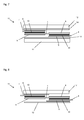
- FIGs. 1 to 8 For illustration of possible zone embodiments of the present invention, reference is also made to Figs. 1 to 8 below.
- the polymer conductor sheet of the present invention is preferably 20 to 400 ⁇ m, more preferably 40 to 300 ⁇ m, most preferably 60 to 200 ⁇ m thick.
- the thickness of each zone of the polymer conductor sheet can vary individually and is preferably 20 to 80%, more preferably 20 to 60%, most preferably 30 to 50% of the total thickness of the polymer conductor sheet. It is also preferred that the thickness of the first zone is 30 to 80% of the thickness or diameter of the at least one conductor, more preferably 40 to 60% of the thickness of the at least one conductor.
- the relative difference in the degree of polymerization and/or crosslinking of the first zone and the second zone preferably is at least 5, 10 or 20%, preferably at least 40 or 50%.
- At least one zone of the polymer conductor sheet is cured to at least 5%, more preferably to at least 15% and most preferably to at least 25%.
- the degree of polymerization is measured according to DIN EN 579:1993-09 replaced by ISO 10147:2011 or EN ISO 10147:2012.
- the polymerization and/or crosslinking of at least one zone is not constant throughout the zone, especially in a direction perpendicular to the flat sides of the sheet.
- Polymerization and/or crosslinking of one zone within the same sheet can be realized by irradiation from one or both sides of the sheet, with the same or different irradiation type(s) or same or different irradiation intensities, thus leading to a changing zone course, possibly due to partial and/or overlapping irradiation.
- a polymer sheet irradiated from both sides can possibly produce an overlap pattern in the center of the sheet, i.e. the overlap region forming a polymerized and/or crosslinked zone.
- Irradiation intensity can be a function of the penetration depth of the irradiation depending on the absorption capacity of the polymer sheet material.
- irradiation energy can be absorbed with penetration depth leading to a gradually changing degree of polymerization and/or crosslinking.
- the degree of polymerization/crosslinking of the polymer conductor sheet can be higher on the sheet's side which faces the irradiation source.
- the zone(s) of the polymer conductor sheet can preferably be irregular or structured due to partial masking of the polymer sheet during irradiation.
- the conductors can partially mask or reflect the irradiation leading to less polymerization in the masked areas and more polymerization and/or crosslinking in the adjacent unmasked areas.
- This partially masked zone could, for example, be more ductile and/or adhesive at the masked conductor contact sites and more stable, i.e. more polymerized and/or more crosslinked in the adjacent regions, thus favoring the fixation of the conductors and at the same time the stability of the sheet.
- a higher degree of polymerization of a zone or portions thereof, e.g. portions not masked by conductors during irradiation may improve the light transmittance of the sheet, preferably for wavelengths used by the current generating element.
- the first zone of the polymer conductor sheet of the present invention has a lower degree of polymerization and/or crosslinking than the second zone and the third zone of same polymer sheet has a lower degree of polymerization and/or crosslinking than the first zone.
- the difference in the degree of polymerization and/or crosslinking in the first, second and/or third zone of the polymer conductor sheet of the present invention is the result of one or more of the following:
- Zone-specific treatment can take place before, during or after positioning the at least one conductor on the sheet.
- the zone-specific treatment can induce, promote or inhibit polymerization and/or crosslinking in the polymeric materials in a controlled manner and the treated materials preferably remain suitable for being laminated to other surfaces.
- the amount, intensity and/or profile of irradiation energy applied, the temperature and/or temperature profile, the concentration of polymerization/crosslinking-inducing, -promoting or -inhibiting chemicals and/or the duration of the treatment lead to controlled degrees of polymerization and/or crosslinking.
- the person skilled in the art will understand that different materials will require different treatment energies, different treatment means/concentrations and/or different treatment profiles.
- Zone-specific irradiation is preferably performed with a high-energy electron beam.
- the radiation dosage may be in the range of 40 to 200 kV, preferably 80 to 120 kV or 10 to 200 kGy depending on the material of the polymeric conductor sheet and depending on the desired degree of polymerization and/or crosslinking.
- zone-specifically irradiate with heat is preferred.
- temperatures applied for heat irradiation are between 20 and 175 °C depending on the material of the polymeric conductor sheet and depending on the desired degree of polymerization and/or crosslinking.
- Ion irradiation can be realized e.g. by generating a plasma.
- zone-specifically irradiate with electro-magnetic energy preferably with light irradiation ranging from IR to UV-light.
- Zone-specific temperature treatment preferably includes the zone-specific application of heat or cold to induce, promote or inhibit polymerization and/or crosslinking.
- zone-specific chemical treatment can be used for influencing the degree of polymerization and/or crosslinking.
- Chemical treatment preferably includes the application of known chemical polymerization and crosslinking inducers, enhancers or inhibitors such as radicals or radical sources (e.g. AIBN, ABCN), peroxides or oxidizing agents (e.g. tert-butylperoxy-2-ethylhexyl carbonate (TBPEHC or TBEC), benzoyl peroxide, hydrogen peroxide, di- tert- butylperoxide, methyl ethyl ketone peroxide, acetone peroxide, peroxydisulfate salts), strong nucleophilic bases (e.g.
- butyllithium, KNH 2 protonic acids (e.g. phosphoric-, sulfuric-, fluoro- and triflic acid), Lewis-Acids (e.g. SnCl 4 , AlCl 3 , BF 3 , TiCl 4 ), metal catalysts (e.g. Ziegler-Natta catalyst, zirconocenes, Phillipps catalyst., nickel or palladium complexes with nitrogen), radical-quenchers (e.g. hydroquinones, monomethylethers of hydroquinones), TAIC (triallyl isocyanate).
- protonic acids e.g. phosphoric-, sulfuric-, fluoro- and triflic acid
- Lewis-Acids e.g. SnCl 4 , AlCl 3 , BF 3 , TiCl 4
- metal catalysts e.g. Ziegler-Natta catalyst, zirconocenes, Phillipps catalyst., nickel or palladium complexes with nitrogen
- the first and/or third zone of the polymer conductor sheet of the present invention is/are adhesive, preferably thermoadhesive at temperatures preferably above 50°C, more preferably above 65°C, most preferably above 89°C, preferably the first zone is ductile, preferably deformable, and the third zone is adhesive.
- the polymer conductor sheet of the present invention can preferably be at least partially transparent.
- Partially transparent means that light is at least partially transmitted through the sheet.
- an at least partially transparent sheet is fully transparent preferably having a transmittance of more than 80% in most of the frequency range relevant for solar cells or semitransparent.
- the at least one elongated conductor of the polymer conductor sheet of the present invention is preferably selected from the group consisting of a wire, strip, ribbon, preferably having a mesh-, web- or grid-like structure.
- the polymer of the polymer conductor sheet of the present invention is selected from the group consisting of thermoplasts, duroplasts, elastomers, and thermoplastic elastomers, preferably polyolefins, polyesters, polyamides, polyimides, polyacrylates, ionomers, polyvinylbutyral (PVB), silicones and polyurethanes (PU), more preferably thermoplastic polyolefins (TPO), polyolefinic elastomers (POE), thermoplastic polyurethanes (TPU), ethylene vinyl acetates (EVAs), polyethylenetetrafluoroethylene (ETFE), polyvinyl chlorides (PVCs), ionomers, polyethylene methacrylic acid (EMA) and polyethylene acrylic acid (EAA), polyethylene terephthalate (PET) and nylon, poly methyl methacrylate (PMMA), polymethacrylate (PMA), , polyvinylsilanes or any combination thereof
- the polymer conductor sheet may consist of a large variety of polymeric materials as well as of their common derivatives.
- such materials can be copolymers of ethylene or copolymers of vinyl acetate and ethylene.
- the polymer sheet materials may be ionomers.
- the acid moieties are randomly or non-randomly distributed in the polymer chain.
- the alpha olefin content of the copolymer preferably ranges from 50-92% while the unsaturated carboxylic acid content of the copolymer preferably ranges from about 2 to 25 mol-%, based on the alpha olefin-acid copolymer; and said acid copolymers preferably feature 10 to 90% of the carboxylic acid groups ionized by neutralization with metal ions from any of the group I, II or III type metals.
- the ionomer may be a sodium ionomer comprising methacrylic acid or a Zn and Na ionomer.
- the polymer may comprise metallocene polyethylene comprising a copolymer (or comonomer) of ethylene and hexene, octene and butene and higher alpha-olefins.
- the metallocene polyethylene is ethylene alpha-olefin comprising comonomer of octene.
- the polymer may be a co-extrusion of Ionomer-Metallocene-polyethylene-Ionomer (IMI).
- the polymer may preferably comprise a polyolefin, more preferably a polyethylene or polypropylene with or without mineral fillers.
- the present invention is directed to a device comprising the polymer conductor sheet of the present invention.
- the device of the present invention is a tabbed solar cell, a solar cell string, matrix or module.
- a tabbed solar cell in the context of the present invention is a polymer conductor sheet conductively connected to a single current generating element, wherein the conductors of the polymer conductor sheet can be connected to further current generating elements.
- a solar cell string according to the invention is a two-dimensional arrangement of at least two solar cells which are conductively interconnected by a polymer conductor sheet.
- a solar cell matrix means a three-dimensional arrangement of solar cells which are conductively interconnected by a polymer conductor sheet.
- a solar cell module refers to solar cell string(s) or matrix(-ces) which are laminated together and may comprise further elements such as e.g. glass plates.
- a solar cell module of the present invention is
- above elements (a) to (d) are connected by lamination. It is further preferred that at least one of the following elements, a zone of the polymer conductor sheet, an encapsulant layer or a back sheet is sufficiently ductile to fill any cavities resulting between the current generating elements (a) and the conductors of the polymer conductor sheets during lamination.
- Figs. 7 and 8 illustrate specific embodiments of the above solar cell modules (I) and (II).
- the light source-facing side of a solar cell module is the side of the module which receives the light, e.g. sun light, for generating an electrical current.
- the light source-averted side of a solar cell module is the side of the module which is facing away from the light source, e.g. the sun.
- the light source is any source which is capable of emitting an energy which a current generating element can transform into an electrical current.
- the solar cell string, matrix or module comprising current generating elements are preferably interconnected by one ore more polymer conductor sheet(s) of the present invention.
- the present invention is directed to a use of a polymer conductor sheet of the present invention for interconnecting current generating elements in a solar cell string, matrix or module.
- the present invention is directed to a method for producing a tabbed solar cell, a solar cell string, matrix or module, comprising the steps of:
- the conductive connection between the conductor component of the polymer conductor sheet and the current generating element is preferably accomplished by attaching, e.g. laminating the first zone of the polymer conductor sheet to the current generating element, preferably while applying heat and/or pressure, preferably under vacuum. During the lamination procedure the first zone holds the conductor(s) in place and its preferably elastomeric and/or adhesive and/or thermoadhesive properties preferably also aid the lamination process.
- conductively connecting the polymer conductor sheet in step (ii) of the above-described method of the invention can also be accomplished without mechanically connecting the at least one conductor with the current generating element, as long as the conduction of electrical current from the current generating element to the conductor is achieved.
- the first zone of the polymer conductor sheet can fill the cavities between the at least one conductor and the current generating element during lamination.
- the polymer conductor sheet of the present invention is pre-fabricated with continuous conductor elements (e.g. continuous wires) and sheets, and preferably stored in the form of a roll. Prior to lamination the roll is uncoiled and preferably cut to size as to agree with the solar cells to be interconnected. One, two or many current generating elements are positioned appropriately onto the polymer conductor sheet and the polymer conductor sheet is attached to produce the solar cell(s).
- continuous conductor elements e.g. continuous wires
- sheets e.g. continuous wires
- the roll Prior to lamination the roll is uncoiled and preferably cut to size as to agree with the solar cells to be interconnected.
- One, two or many current generating elements are positioned appropriately onto the polymer conductor sheet and the polymer conductor sheet is attached to produce the solar cell(s).
- At least one polymer conductor sheet of the present invention is aligned, contacted and connected to each side of at least one current generating element in the method according to the present invention.
- At least one polymer conductor sheet of the present invention is aligned, contacted and connected to at least one side of at least two current generating elements, thus mechanically and electrically interconnecting said elements according to the method of the present invention.
- the conductor elements may be conductively connected to the current generating element(s) prior to further lamination, e.g. by induction or laser soldering, or during lamination of a solar module.
- the polymer conductor sheet(s) is/are preferably connected to the current generating element in a laminator.
- the present invention is directed to a method for forming a polymer conductor sheet according to the invention, comprising the steps of:
- Step d) may be carried out after step b) or prior to it.
- Figure 1 shows a side view of a polymer sheet (1) comprising two adjacent zones (2) and (3) within the same polymer sheet (1), the first zone (3) extending between the second zone (2) and the flat side 15 of the sheet.
- the second zone (2) has a higher degree of polymerization and/or crosslinking and has a higher stability due to polymerizing and/or crosslinking than the first zone (3)
- the first zone (3) is more ductile and/or adhesive and has a lower degree of polymerization and/or crosslinking than the second zone (2) due to no or less polymerizing and/or crosslinking than the second zone (2).
- Elongated conductors (4) (extending in the direction perpendicular to the plane of the figure) are positioned on and held by the less polymerized and/or crosslinked first zone (3).
- the degree of polymerization and/or crosslinking is depicted as function of the location in the polymer sheet (1).
- Figure 2 shows a side view of a polymer sheet (1) comprising two adjacent zones (2) and (3) within the same polymer sheet (1).
- the first zone (3) has a higher degree of polymerization and/or crosslinking and has a higher stability due to polymerizing and/or crosslinking than the second zone (2)
- the second zone (2) is more ductile and/or adhesive and has a lower degree of polymerization and/or crosslinking than the first zone (3) due to no or less polymerizing and/or crosslinking than the first zone (3).
- Elongated conductors (4) (extending in the direction perpendicular to the plane of the figure) are positioned on and held by the more polymerized and/or crosslinked first zone (3).
- Figure 3 shows a side view of a polymer sheet (5) comprising three adjacent zones (2), (3) and (6) within the same polymer sheet (5).
- the second zone (2) has a higher degree of polymerization and/or crosslinking and has a higher stability due to polymerizing and/or crosslinking than the first zone (3)
- the first zone (3) is more ductile and/or adhesive and has a lower degree of polymerization and/or crosslinking than the second zone (2) due to no or less polymerizing and/or crosslinking than the second zone (2).
- Elongated conductors (4) are positioned on the less polymerized and/or crosslinked first zone (3).
- the third zone (6) located adjacent to the second zone (2) is more ductile and/or adhesive and has a lower degree of polymerization and/or crosslinking than the second zone (2) due to no or less polymerizing and/or crosslinking than the second zone (2) and has a lower degree of polymerization and/or crosslinking than the first zone (3).
- Figure 4 is a diagram (comparable to those to the left in figures 1 to 3 ) showing the degree of polymerization and/or crosslinking on the y-axis (7) as a function of a first, second and third zone (3, 2 and 6) of a polymer conductor sheet (1) on the x-axis (8).
- Figure 5 shows two polymer conductor sheet (9) interconnected by elongated conductors (4).
- the sheets are positioned such that the first zone (3) of the left polymer sheet (9) is facing up thus rendering the conductors (4) visible and the first zone (3) of the right sheet (9) is facing down covering the conductors.
- Figure 6 shows two current generating elements (10) interconnected by the conductors (4) of two polymer conductor sheets (9).
- Figure 7 shows a lay-up for a solar module (11) comprising two current generating elements (10) interconnected by the elongated conductors (4) of two polymer conductor sheets (9).
- the elongated conductors (4) of the respective polymer conductor sheets (9) extend out of the solar module (11).
- Encapsulant layers (14) mechanically connect two glass plates (12) to the polymer conductor sheets (9), which glass plates (12) form the outer hull of the solar module after lamination.
- Figure 8 shows a lay-up without encapsulant layers.
- the polymer conductor sheets (9) are large enough to fill cavities between the current generating elements (10), conductors (4) and the glass plate (12) / back sheet (13).
- the side of the solar module not facing the sun is covered by a back sheet (13) which can be opaque.
- a non-limiting example for the production of a polymer conductor sheet and a solar cell module according to the present invention is provided.
- PV-FS CVF sheet (dnpSolar, Karlslunde, Denmark) of 400 ⁇ m thickness was irradiated with 200 kV acceleration voltage using an EBlab e-beam device (ebeam Technologies, COMET AG, Flamatt, Switzerland).
- This irradiation step polymerized and/or crosslinked the first zone of the polymer sheet facing the irradiation source with a complex viscosity of about 4 x 10 4 Pas at 85 °C, the rest of the sheet forming the second zone with less polymerization and/or crosslinking.
Landscapes
- Photovoltaic Devices (AREA)
- Engineering & Computer Science (AREA)
- Mechanical Engineering (AREA)
Abstract
Description
- The present invention relates to polymer conductor sheets comprising zones featuring different degrees of polymerization and/or crosslinking within the same polymer sheet, wherein the zones differ, for example, in mechanical stability, ductility and/or (thermo)adhesiveness. The present invention also teaches devices comprising these zoned polymer conductor sheets such as solar cell strings, matrices and modules, uses thereof and methods for producing these.
- Electrically conducting connections within a solar cell or between solar cells in a solar cell array are usually achieved by soldering individual electrical conductors or grids of electrical conductors onto the current-generating element of solar cells. Current generating elements in the context of solar cells include p-n elements, organic current generating elements such as Grätzel-cells. Polymeric materials are commonly used in the manufacture of solar cells to encapsulate and protect the solar cells against various external influences.
-
US 6,586,271 B1 describes homogenously polymerized materials with high thermal creep resistance manufactured by irradiation-induced polymerization. Said polymers are used in various places in the solar cell and the polymers can be combined with a metal interconnection pattern placed on the backskin layer of the solar cell. This metal interconnection pattern is soldered or bonded to the solar cell by conductive epoxy after positioning the pattern onto the backskin material. -
WO 2011/089473 describes a system and method for laminating solar cells with a membrane or an adhesive foil in order to press a plurality of layers of the solar cell together.WO 2004/021455 is directed to attaching conductive wires to an adhesive layer which in turn is attached to a separate, optically transparent and electrically insulating film. The adhesive layer and the insulating film are made of chemically different materials. The adhesive foil with the wires attached is then contacted with a surface of a p-n element. - It is the objective of the present invention to provide new and improved means for efficient and economic solar cell production.
- This objective is solved by a polymer conductor sheet comprising
- (i) a polymer sheet comprising at least two adjacent zones within the same polymer sheet, which zones run in longitudinal direction of the polymer sheet, wherein
- (1) a first zone is sufficiently ductile and/or adhesive to fix the position of an elongated conductor on its surface facing the outside of the polymer sheet, and
- (2) a second zone adjacent to the first zone that has a different degree of polymerization and/or crosslinking than the first zone, and
- (ii) at least one elongated conductor positioned on the surface of the first zone facing the outside of the polymer sheet.
- The polymer sheet comprising the at least two adjacent zones and for use according to the present invention is produced from one or more monomers. The polymer sheet for use in the present invention is a chemically homogenous material with regard to its original monomer composition. The differences in the degree of polymerization and/or the degree of crosslinking that distinguish the adjacent zones within the same polymer sheet are the result of positionally limited, i.e. zone-specific polymerization and/or crosslinking. In other words, the at least two adjacent zones are the result of different degrees of polymerization and/or crosslinking of the same starting materials. This starting material is also termed polymerizable sheet. For example, the different zones can be the result of zone-specific treatment of monomers or polymers that are (further) polymerized and/or (further) cross-linked, e.g. by zone-specific irradiation, zone-specific temperature control, and/or zone-specific chemical treatment. Contrary to an assembly of separate layers with different chemical compositions which were produced separately, the polymer sheet of the present invention is the result of the same homogenous starting materials in one sheet that is treated positionally different for polymerization and/or crosslinking. Because the zones form part of the same polymer sheet the zones are directly adjacent to and closely in contact with each other, forming a polymerized transition zone. The transition from one zone to the adjacent zone may be continuous, gradual or sharp in the sense that the degree of polymerization and/or crosslinking from one zone to the other zone can change abruptly or continuously within the polymer sheet. The zones of the polymer sheet for use in the present invention are not the result of a step-wise assembly of different and/or separate layers but are individual zones encompassed within the same polymer matrix sheet, which zones differ in their degree of polymerization and or crosslinking.
- As generally understood, a polymer is the result of a reaction between identical or different monomers. The degree of polymerization is commonly known as the number of monomeric units in the polymer. Crosslinking refers to producing one or more bonds that link one polymer part to another polymer part, possibly parts of the same or different polymers, e.g. by covalent or ionic bonds.
- Polymers with identical composition but different degrees of polymerization and/or crosslinking typically exhibit different physical and/or chemical properties. In general, increasing the degree of polymerization and/or crosslinking correlates with higher melting temperature and higher mechanical strength of the polymer.
- The zones within the polymer conductor sheet run in the longitudinal direction of the polymer sheet, i.e. parallel to the flat sides of the sheet. Also, the zones of the polymer conductor sheet are located one above the other in the longitudinal direction. Preferably, the zones may be overlapping.
- According to the invention, one zone can provide increased stability for the entire sheet due to its higher degree of polymerization and/or crosslinking compared to the less polymerized and/or crosslinked other zone(s). One zone can be more ductile, less rigid and possibly even adhesive or thermoadhesive compared to the other zone(s), thus allowing for e.g. laminating the polymer conductor sheet to a current generating element or to a glass surface. The first zone is suited for receiving, fixing and possibly even conforming to some extent to the shape of a current generating element(s) and/or a conductor(s) such as, e.g. a wire or a wire web.
- A conductor is any means capable of conducting an electrical current. For example, it may be in the form of a wire, a bar, an electrode or an assembly of wires, e.g. a wire web, bars or electrodes. Typically, a conductor is a metallic structure which may not be self-supporting and which may be applied e.g. by electroplating or plasma spraying. The conductor may comprise an alloy on its surface which alloy may form a solder connection or form an eutectic system with the surface that is to be connected to the conductor, e.g. a current generating element for solar cell production. It may also be coated with a material for optical and/or aesthetic reasons.
- Two or more polymer conductor sheets may be interconnected by their conductors, preferably by their conductor web. In other words, two or more polymer sheets may be positioned on the same conductor, preferably conductor web, at different sites of the conductor, thus forming polymer conductor sheets which are interconnected by the same conductor or conductor web.
- The term current generating element for use according to the present invention is meant to encompass a p-n junction element, an organic current generating element or a dye-sensitized solar cell such as the Grätzel cell. Typically, a p-n junction element is the boundary element or interface between two types of semiconductor materials (p-type and n-type) inside a single crystal of a semiconductor which may form part of a solar cell. An organic current generating element is typically produced from conductive organic polymers or conductive small organic molecules. A dye-sensitized solar cell is based on a semiconductor formed between a photo-sensitized anode and an electrolyte forming a photoelectrochemical system.
- The conductor positioned on the first zone of the polymer sheet can be stabilized in its position on the polymer sheet due to the ductile and/or (thermo)adhesive properties of the latter, thus allowing for spatial fixation of the conductor(s) on the polymer sheet during assembly, transport and/or final application of the polymer conductor sheet, e.g. to a current generating element for producing a solar cell.
- The term adhesive as used herein means that the adhesive zone receives and positionally fixates the at least one conductor and encompasses the term thermoadhesive. Thermoadhesive means that the adhesive properties of a zone are a function of its temperature, e.g. the zone will be more adhesive when heated. Receiving and fixating the at least one conductor can be the result of adhesive forces and/or of the ductile properties and/or adaption of the zone to the shape of the at least one conductor, thus preventing lateral movement on the sheet and/or separation of the conductor from the first zone. The term adhesive is not limited to a sticky surface but preferably characterizes any adhering of the conductor(s) to the first zone. Ductile as used herein means that the zone can adjust three-dimensionally to the shape of the at least one conductor.
- The first zone of the polymer sheet may only embed part of the conductor(s) so that a protruding part of the conductor can still contact the device of interest, e.g. a current generating element for producing a solar cell.
- In a preferred embodiment, the polymer conductor sheet of the present invention further comprises a third zone within the same polymer sheet that has a different degree of polymerization and/or crosslinking than the second zone, wherein the third zone is located adjacent to the second zone.
- In a further preferred embodiment, the third zone of the polymer sheet of the present invention has a lower degree of polymerization and/or crosslinking than the second zone, preferably also lower than the first zone.
- For example, a polymer conductor sheet of the present invention may be of the following structure comprising three zones: A first zone receiving the at least one conductor which is less polymerized and/or crosslinked compared to the adjacent second zone. The more polymerized second zone provides stability for the polymer conductor sheet due to its higher degree of polymerization and/or crosslinking compared to the first zone. A third zone is located adjacent to the second zone, which third zone is less polymerized and/or crosslinked compared to the first and second zone. The low degree of polymerization of the third zone facilitates the adhesion of the polymer conductor sheet via its third zone to an exterior surface, e.g. a glass plate. For illustration of possible zone embodiments of the present invention, reference is also made to
Figs. 1 to 8 below. - The polymer conductor sheet of the present invention is preferably 20 to 400 µm, more preferably 40 to 300 µm, most preferably 60 to 200 µm thick. The thickness of each zone of the polymer conductor sheet can vary individually and is preferably 20 to 80%, more preferably 20 to 60%, most preferably 30 to 50% of the total thickness of the polymer conductor sheet. It is also preferred that the thickness of the first zone is 30 to 80% of the thickness or diameter of the at least one conductor, more preferably 40 to 60% of the thickness of the at least one conductor.
- The relative difference in the degree of polymerization and/or crosslinking of the first zone and the second zone preferably is at least 5, 10 or 20%, preferably at least 40 or 50%.
- Preferably at least one zone of the polymer conductor sheet is cured to at least 5%, more preferably to at least 15% and most preferably to at least 25%. The degree of polymerization is measured according to DIN EN 579:1993-09 replaced by ISO 10147:2011 or EN ISO 10147:2012.
- It is preferred that the polymerization and/or crosslinking of at least one zone is not constant throughout the zone, especially in a direction perpendicular to the flat sides of the sheet.
- Polymerization and/or crosslinking of one zone within the same sheet can be realized by irradiation from one or both sides of the sheet, with the same or different irradiation type(s) or same or different irradiation intensities, thus leading to a changing zone course, possibly due to partial and/or overlapping irradiation. For example, a polymer sheet irradiated from both sides can possibly produce an overlap pattern in the center of the sheet, i.e. the overlap region forming a polymerized and/or crosslinked zone. Irradiation intensity can be a function of the penetration depth of the irradiation depending on the absorption capacity of the polymer sheet material. In other words, irradiation energy can be absorbed with penetration depth leading to a gradually changing degree of polymerization and/or crosslinking. For example, the degree of polymerization/crosslinking of the polymer conductor sheet can be higher on the sheet's side which faces the irradiation source.
- The zone(s) of the polymer conductor sheet can preferably be irregular or structured due to partial masking of the polymer sheet during irradiation. For example, if the conductors are applied to the first receiving zone prior to irradiation, the conductors can partially mask or reflect the irradiation leading to less polymerization in the masked areas and more polymerization and/or crosslinking in the adjacent unmasked areas. This partially masked zone could, for example, be more ductile and/or adhesive at the masked conductor contact sites and more stable, i.e. more polymerized and/or more crosslinked in the adjacent regions, thus favoring the fixation of the conductors and at the same time the stability of the sheet. Also, a higher degree of polymerization of a zone or portions thereof, e.g. portions not masked by conductors during irradiation, may improve the light transmittance of the sheet, preferably for wavelengths used by the current generating element.
- In a further preferred embodiment the first zone of the polymer conductor sheet of the present invention has a lower degree of polymerization and/or crosslinking than the second zone and the third zone of same polymer sheet has a lower degree of polymerization and/or crosslinking than the first zone.
- In yet another preferred embodiment, the difference in the degree of polymerization and/or crosslinking in the first, second and/or third zone of the polymer conductor sheet of the present invention is the result of one or more of the following:
- 1. zone-specific irradiation, preferably electron, ion, atomic, heat or electro-magnetic irradiation,
- 2. zone-specific temperature treatment,
- 3. zone-specific chemical treatment
- Zone-specific treatment can take place before, during or after positioning the at least one conductor on the sheet. The zone-specific treatment can induce, promote or inhibit polymerization and/or crosslinking in the polymeric materials in a controlled manner and the treated materials preferably remain suitable for being laminated to other surfaces. The amount, intensity and/or profile of irradiation energy applied, the temperature and/or temperature profile, the concentration of polymerization/crosslinking-inducing, -promoting or -inhibiting chemicals and/or the duration of the treatment lead to controlled degrees of polymerization and/or crosslinking. The person skilled in the art will understand that different materials will require different treatment energies, different treatment means/concentrations and/or different treatment profiles.
- Zone-specific irradiation is preferably performed with a high-energy electron beam. The radiation dosage may be in the range of 40 to 200 kV, preferably 80 to 120 kV or 10 to 200 kGy depending on the material of the polymeric conductor sheet and depending on the desired degree of polymerization and/or crosslinking.
- Also, it is preferred to zone-specifically irradiate with heat. Typically the temperatures applied for heat irradiation are between 20 and 175 °C depending on the material of the polymeric conductor sheet and depending on the desired degree of polymerization and/or crosslinking.
- Ion irradiation can be realized e.g. by generating a plasma.
- Furthermore, it is preferred to zone-specifically irradiate with electro-magnetic energy, preferably with light irradiation ranging from IR to UV-light.
- Modifying the properties of polymers by atomic radiation is common general knowledge and has been published, e.g. in the textbook "Atomic Radiation and Polymers", A Charlesby, Pergamon Press, NY, 1960.
- Zone-specific temperature treatment preferably includes the zone-specific application of heat or cold to induce, promote or inhibit polymerization and/or crosslinking.
- Also, zone-specific chemical treatment can be used for influencing the degree of polymerization and/or crosslinking. Chemical treatment preferably includes the application of known chemical polymerization and crosslinking inducers, enhancers or inhibitors such as radicals or radical sources (e.g. AIBN, ABCN), peroxides or oxidizing agents (e.g. tert-butylperoxy-2-ethylhexyl carbonate (TBPEHC or TBEC), benzoyl peroxide, hydrogen peroxide, di-tert-butylperoxide, methyl ethyl ketone peroxide, acetone peroxide, peroxydisulfate salts), strong nucleophilic bases (e.g. butyllithium, KNH2), protonic acids (e.g. phosphoric-, sulfuric-, fluoro- and triflic acid), Lewis-Acids (e.g. SnCl4, AlCl3, BF3, TiCl4), metal catalysts (e.g. Ziegler-Natta catalyst, zirconocenes, Phillipps catalyst., nickel or palladium complexes with nitrogen), radical-quenchers (e.g. hydroquinones, monomethylethers of hydroquinones), TAIC (triallyl isocyanate).
- In a further preferred embodiment, the first and/or third zone of the polymer conductor sheet of the present invention is/are adhesive, preferably thermoadhesive at temperatures preferably above 50°C, more preferably above 65°C, most preferably above 89°C, preferably the first zone is ductile, preferably deformable, and the third zone is adhesive.
- The polymer conductor sheet of the present invention can preferably be at least partially transparent.
- Partially transparent means that light is at least partially transmitted through the sheet. Preferably, an at least partially transparent sheet is fully transparent preferably having a transmittance of more than 80% in most of the frequency range relevant for solar cells or semitransparent.
- The at least one elongated conductor of the polymer conductor sheet of the present invention is preferably selected from the group consisting of a wire, strip, ribbon, preferably having a mesh-, web- or grid-like structure.
- In a yet another preferred embodiment, the polymer of the polymer conductor sheet of the present invention is selected from the group consisting of thermoplasts, duroplasts, elastomers, and thermoplastic elastomers, preferably polyolefins, polyesters, polyamides, polyimides, polyacrylates, ionomers, polyvinylbutyral (PVB), silicones and polyurethanes (PU), more preferably thermoplastic polyolefins (TPO), polyolefinic elastomers (POE), thermoplastic polyurethanes (TPU), ethylene vinyl acetates (EVAs), polyethylenetetrafluoroethylene (ETFE), polyvinyl chlorides (PVCs), ionomers, polyethylene methacrylic acid (EMA) and polyethylene acrylic acid (EAA), polyethylene terephthalate (PET) and nylon, poly methyl methacrylate (PMMA), polymethacrylate (PMA), , polyvinylsilanes or any combination thereof.
- The polymer conductor sheet may consist of a large variety of polymeric materials as well as of their common derivatives. For example, such materials can be copolymers of ethylene or copolymers of vinyl acetate and ethylene.
- Also, the polymer sheet materials may be ionomers. Ionomers can be derived from any direct or grafted ethylene copolymer of an alpha olefin having the formula R-CH=CH2, where R is a radical selected from the group consisting of hydrogen and aryl radicals preferably featuring from 1 to 8 carbon atoms and alpha, beta-ethylenically unsaturated carboxylic acid preferably featuring from 3 to 8 carbon atoms or longer. The acid moieties are randomly or non-randomly distributed in the polymer chain. The alpha olefin content of the copolymer preferably ranges from 50-92% while the unsaturated carboxylic acid content of the copolymer preferably ranges from about 2 to 25 mol-%, based on the alpha olefin-acid copolymer; and said acid copolymers preferably feature 10 to 90% of the carboxylic acid groups ionized by neutralization with metal ions from any of the group I, II or III type metals. In a more preferred embodiment, the ionomer may be a sodium ionomer comprising methacrylic acid or a Zn and Na ionomer. Also, the polymer may comprise metallocene polyethylene comprising a copolymer (or comonomer) of ethylene and hexene, octene and butene and higher alpha-olefins. In a preferred embodiment, the metallocene polyethylene is ethylene alpha-olefin comprising comonomer of octene. Also, the polymer may be a co-extrusion of Ionomer-Metallocene-polyethylene-Ionomer (IMI).
- Furthermore, the polymer may preferably comprise a polyolefin, more preferably a polyethylene or polypropylene with or without mineral fillers.
- In a second aspect, the present invention is directed to a device comprising the polymer conductor sheet of the present invention.
- In a preferred embodiment, the device of the present invention is a tabbed solar cell, a solar cell string, matrix or module. A tabbed solar cell in the context of the present invention is a polymer conductor sheet conductively connected to a single current generating element, wherein the conductors of the polymer conductor sheet can be connected to further current generating elements.
- A solar cell string according to the invention is a two-dimensional arrangement of at least two solar cells which are conductively interconnected by a polymer conductor sheet. A solar cell matrix means a three-dimensional arrangement of solar cells which are conductively interconnected by a polymer conductor sheet. A solar cell module refers to solar cell string(s) or matrix(-ces) which are laminated together and may comprise further elements such as e.g. glass plates.
- In another preferred embodiment, a solar cell module of the present invention is
- (I) a solar cell module having a top and bottom side comprising:
- (a) at least two current generating elements,
- (b) at least two polymer conductor sheets,
- (c) optionally at least two encapsulant layers, and
- (d) at least two glass plates,
wherein- (i) at least two current generating elements (a) are conductively interconnected by the conductors of the at least two polymer conductor sheets (b) to form a solar cell string, and
- (iia) the glass plates (d) are connected to the polymer conductor sheets (b) on the top and bottom sides of the solar module, which glass plates form the outer surface of the solar cell module, or
- (iib) the optional encapsulant layers (c) connect the glass plates (d) to the polymer conductor sheets (b) on the top and/or bottom side of the solar module, which glass plates form the outer surface of the solar module;
or
- (II) a solar cell module having a light source-facing and a light source-averted side comprising:
- (a) at least two current generating elements,
- (b) at least two polymer conductor sheets,
- (b2) optionally at least two encapsulant layers,
- (c) a back sheet, preferably an opaque back sheet, and
- (d) a glass plate,
wherein- (i) at least two current generating elements (a) are conductively interconnected by the conductors of the at least two polymer conductor sheets (b),
- (ii) the back sheet (c) is connected to the polymer conductor sheet (b) on the light source-averted side of the solar module,
- (iii) the glass plate (d) is connected to the polymer conductor sheet (b) on the light source-facing side of the solar module, and
- (iv) the optional encapsulant layers (b2) connect the glass plate (d) and/or the back sheet (c) to the polymer conductor sheets (b) on the top and bottom side of the solar module, respectively, which glass plate and back sheet form the outer surface of the solar module.
- It is preferred that above elements (a) to (d) are connected by lamination. It is further preferred that at least one of the following elements, a zone of the polymer conductor sheet, an encapsulant layer or a back sheet is sufficiently ductile to fill any cavities resulting between the current generating elements (a) and the conductors of the polymer conductor sheets during lamination.
-
Figs. 7 and 8 illustrate specific embodiments of the above solar cell modules (I) and (II). The light source-facing side of a solar cell module is the side of the module which receives the light, e.g. sun light, for generating an electrical current. The light source-averted side of a solar cell module is the side of the module which is facing away from the light source, e.g. the sun. The light source is any source which is capable of emitting an energy which a current generating element can transform into an electrical current. - The solar cell string, matrix or module comprising current generating elements are preferably interconnected by one ore more polymer conductor sheet(s) of the present invention.
- In a third aspect, the present invention is directed to a use of a polymer conductor sheet of the present invention for interconnecting current generating elements in a solar cell string, matrix or module.
- In a fourth aspect, the present invention is directed to a method for producing a tabbed solar cell, a solar cell string, matrix or module, comprising the steps of:
- (i) providing a polymer conductor sheet according to the invention, and
- (ii) aligning and contacting the polymer conductor sheet of step (i) to at least one current generating element, and
- (iii) conductively connecting the polymer conductor sheet to the at least one current generating element, optionally under pressure and/or heat.
- The conductive connection between the conductor component of the polymer conductor sheet and the current generating element is preferably accomplished by attaching, e.g. laminating the first zone of the polymer conductor sheet to the current generating element, preferably while applying heat and/or pressure, preferably under vacuum. During the lamination procedure the first zone holds the conductor(s) in place and its preferably elastomeric and/or adhesive and/or thermoadhesive properties preferably also aid the lamination process. However, conductively connecting the polymer conductor sheet in step (ii) of the above-described method of the invention can also be accomplished without mechanically connecting the at least one conductor with the current generating element, as long as the conduction of electrical current from the current generating element to the conductor is achieved. In a preferred embodiment, the first zone of the polymer conductor sheet can fill the cavities between the at least one conductor and the current generating element during lamination.
- It is preferred that the polymer conductor sheet of the present invention is pre-fabricated with continuous conductor elements (e.g. continuous wires) and sheets, and preferably stored in the form of a roll. Prior to lamination the roll is uncoiled and preferably cut to size as to agree with the solar cells to be interconnected. One, two or many current generating elements are positioned appropriately onto the polymer conductor sheet and the polymer conductor sheet is attached to produce the solar cell(s).
- In a preferred embodiment, at least one polymer conductor sheet of the present invention is aligned, contacted and connected to each side of at least one current generating element in the method according to the present invention.
- In a further preferred embodiment, at least one polymer conductor sheet of the present invention is aligned, contacted and connected to at least one side of at least two current generating elements, thus mechanically and electrically interconnecting said elements according to the method of the present invention.
- The conductor elements may be conductively connected to the current generating element(s) prior to further lamination, e.g. by induction or laser soldering, or during lamination of a solar module.
- The polymer conductor sheet(s) is/are preferably connected to the current generating element in a laminator.
- In a fifth aspect, the present invention is directed to a method for forming a polymer conductor sheet according to the invention, comprising the steps of:
- a) providing a polymerizable sheet that can be at least partially polymerized and/or crosslinked;
- b) polymerizing and/or crosslinking the polymerizable sheet zone-specifically to generate a first, second and/or third zone within the same polymer sheet by one or more treatments selected from the group consisting of:
- zone-specific irradiation, preferably electron, ion, atomic, neutron, heat or electro-magnetic irradiation,
- zone-specific temperature treatment, and
- zone-specific chemical treatment
within the same polymer sheet;
- c) providing an elongated conductor; and
- d) positioning, preferably temporarily attaching, the elongated conductor on the surface of the first zone facing the outside of the polymer sheet.
- In the following the present invention will be further illustrated by way of figures, which represent specific and non-limiting embodiments of the invention, none of which are to be considered as limiting the invention beyond the scope of the appended claims. In the Figures, identical, functionally identical or similar parts are shown with the same reference number.
-
- Fig. 1
- shows a polymer conductor sheet with two zones and conductors
- Fig. 2
- shows a polymer conductor sheet with two zones and conductors
- Fig. 3
- shows a polymer conductor sheet with three zones and conductors
- Fig. 4
- is a diagram showing the degree of polymerization and/or crosslinking as a function of zones
- Fig. 5
- shows two polymer conductor sheets with connectors
- Fig. 6
- shows two solar cells interconnected by the conductors of two polymer conductor sheets
- Fig. 7
- shows a lay-up for a solar module with an encapsulant layer
- Fig. 8
- shows a lay-up for a solar module without encapsulant layer
-
- 1
- polymer conductor sheet with 2 zones
- 2
- second zone
- 3
- first zone
- 4
- conductor(s)
- 5
- polymer conductor sheet with 3 zones
- 6
- third zone
- 7
- y-axis (degree of polymerization and/or crosslinking)
- 8
- x-axis
- 9
- polymer conductor sheet
- 10
- current generating element
- 11
- lay-up for a solar module
- 12
- glass plate
- 13
- back sheet
- 14
- encapsulant layer
- 15
- flat side of the sheet
-
Figure 1 shows a side view of a polymer sheet (1) comprising two adjacent zones (2) and (3) within the same polymer sheet (1), the first zone (3) extending between the second zone (2) and theflat side 15 of the sheet. The second zone (2) has a higher degree of polymerization and/or crosslinking and has a higher stability due to polymerizing and/or crosslinking than the first zone (3), and the first zone (3) is more ductile and/or adhesive and has a lower degree of polymerization and/or crosslinking than the second zone (2) due to no or less polymerizing and/or crosslinking than the second zone (2). Elongated conductors (4) (extending in the direction perpendicular to the plane of the figure) are positioned on and held by the less polymerized and/or crosslinked first zone (3). To the left offigures 1 to 3 the degree of polymerization and/or crosslinking is depicted as function of the location in the polymer sheet (1). -
Figure 2 shows a side view of a polymer sheet (1) comprising two adjacent zones (2) and (3) within the same polymer sheet (1). The first zone (3) has a higher degree of polymerization and/or crosslinking and has a higher stability due to polymerizing and/or crosslinking than the second zone (2), and the second zone (2) is more ductile and/or adhesive and has a lower degree of polymerization and/or crosslinking than the first zone (3) due to no or less polymerizing and/or crosslinking than the first zone (3). Elongated conductors (4) (extending in the direction perpendicular to the plane of the figure) are positioned on and held by the more polymerized and/or crosslinked first zone (3). -
Figure 3 shows a side view of a polymer sheet (5) comprising three adjacent zones (2), (3) and (6) within the same polymer sheet (5). The second zone (2) has a higher degree of polymerization and/or crosslinking and has a higher stability due to polymerizing and/or crosslinking than the first zone (3), the first zone (3) is more ductile and/or adhesive and has a lower degree of polymerization and/or crosslinking than the second zone (2) due to no or less polymerizing and/or crosslinking than the second zone (2). Elongated conductors (4) are positioned on the less polymerized and/or crosslinked first zone (3). The third zone (6) located adjacent to the second zone (2) is more ductile and/or adhesive and has a lower degree of polymerization and/or crosslinking than the second zone (2) due to no or less polymerizing and/or crosslinking than the second zone (2) and has a lower degree of polymerization and/or crosslinking than the first zone (3). -
Figure 4 is a diagram (comparable to those to the left infigures 1 to 3 ) showing the degree of polymerization and/or crosslinking on the y-axis (7) as a function of a first, second and third zone (3, 2 and 6) of a polymer conductor sheet (1) on the x-axis (8). -
Figure 5 shows two polymer conductor sheet (9) interconnected by elongated conductors (4). The sheets are positioned such that the first zone (3) of the left polymer sheet (9) is facing up thus rendering the conductors (4) visible and the first zone (3) of the right sheet (9) is facing down covering the conductors. -
Figure 6 shows two current generating elements (10) interconnected by the conductors (4) of two polymer conductor sheets (9). -
Figure 7 shows a lay-up for a solar module (11) comprising two current generating elements (10) interconnected by the elongated conductors (4) of two polymer conductor sheets (9). The elongated conductors (4) of the respective polymer conductor sheets (9) extend out of the solar module (11). Encapsulant layers (14) mechanically connect two glass plates (12) to the polymer conductor sheets (9), which glass plates (12) form the outer hull of the solar module after lamination. -
Figure 8 shows a lay-up without encapsulant layers. Here, the polymer conductor sheets (9) are large enough to fill cavities between the current generating elements (10), conductors (4) and the glass plate (12) / back sheet (13). The side of the solar module not facing the sun is covered by a back sheet (13) which can be opaque. - A non-limiting example for the production of a polymer conductor sheet and a solar cell module according to the present invention is provided.
- A PV-FS CVF sheet (dnpSolar, Karlslunde, Denmark) of 400 µm thickness was irradiated with 200 kV acceleration voltage using an EBlab e-beam device (ebeam Technologies, COMET AG, Flamatt, Switzerland). This irradiation step polymerized and/or crosslinked the first zone of the polymer sheet facing the irradiation source with a complex viscosity of about 4 x 10⁴ Pas at 85 °C, the rest of the sheet forming the second zone with less polymerization and/or crosslinking.
- Subsequently, a grid of conductors was placed on the first zone of the polymer sheet, thus yielding a polymer conductor sheet. By heating the conductors, the first zone was locally melted thus rendering it adhesive enough to hold the conductors.
- Current generating elements were laminated for 20 minutes at a maximum temperature of 170 °C with the above polymer conductor sheets, two layers of PV-FS CVF sheet (dnpSolar, Karlslunde, Denmark) of 400 µm thickness on opposite sides and two 3.2 mm thick glass plates on opposite sides (solar grade glass, f| solar GmbH, Suelzetal, Germany) yielding a solar cell module with the build-up as shown in
Figure 7 .
Claims (15)
- A polymer conductor sheet comprising(i) a polymer sheet comprising at least two adjacent zones within the same polymer sheet, which zones run in longitudinal direction of the polymer sheet, wherein(1) a first zone is sufficiently ductile and/or adhesive to fix the position of an elongated conductor on its surface facing the outside of the polymer sheet, and(2) a second zone adjacent to the first zone that has a different degree of polymerization and/or crosslinking than the first zone, and(ii) at least one elongated conductor positioned on the surface of the first zone facing the outside of the polymer sheet.
- The polymer conductor sheet of claim 1, further comprising a third zone within the same polymer sheet that has a different degree of polymerization and/or crosslinking than the second zone, wherein the third zone is located adjacent to the second zone.
- The polymer conductor sheet of claim 2, wherein the third zone within the same polymer sheet has a lower degree of polymerization and/or crosslinking than the second zone, preferably also lower than the first zone.
- The polymer conductor sheet of any of claims 2 and 3, wherein the first zone within the same polymer sheet has a lower degree of polymerization and/or crosslinking than the second zone and the third zone within the same polymer sheet has a lower degree of polymerization and/or crosslinking than the first zone.
- The polymer conductor sheet of claims 1 to 4, wherein the difference in the degree of polymerization and/or crosslinking in the first, second and/or third zone is the result of one or more of the following:1. zone-specific irradiation, preferably electron, ion, atomic, neutron, heat or electro-magnetic irradiation,2. zone-specific temperature treatment,3. zone-specific chemical treatment
within the same polymer sheet. - The polymer conductor sheet of any of claims 1 to 5, wherein the first and/or third zone is/are thermoadhesive, preferably wherein the first zone is ductile and the third zone is thermoadhesive.
- The polymer conductor sheet of any of claims 1 to 6, wherein the polymer is selected from the group consisting of thermoplasts, duroplasts, elastomers, and thermoplastic elastomers, preferably polyolefins, polyesters, polyamides, polyimides, polyacrylates, ionomers, polyvinylbutyral (PVB), silicones and polyurethanes (PU), more preferably thermoplastic polyolefins (TPO), polyolefinic elastomers (POE), thermoplastic polyurethanes (TPU), ethylene vinyl acetates (EVAs), polyethylenetetrafluoroethylene (ETFE), polyvinyl chlorides (PVCs), ionomers, polyethylene methacrylic acid (EMA) and polyethylene acrylic acid (EAA), polyethylene terephthalate (PET) and nylon, poly methyl methacrylate (PMMA), polymethacrylate (PMA), , polyvinylsilanes or any combination thereof.
- A Device comprising a polymer conductor sheet of any of claims 1 to 7.
- The device according to claim 8, wherein the device is a tabbed solar cell, a solar cell string, matrix or module, preferably comprising current generating elements interconnected by a polymer conductor sheet of any of claims 1 to 7
- The device according to claim 9, wherein the solar cell module is(I) a solar cell module having a top and bottom side comprising:(a) at least two current generating elements,(b) at least two polymer conductor sheets,(c) optionally at least two encapsulant layers, and(d) at least two glass plates,
wherein(ii) at least two current generating elements (a) are conductively interconnected by the conductors of the at least two polymer conductor sheets (b) to form a solar cell string, and(iia) the glass plates (d) are connected to the polymer conductor sheets (b) on the top and bottom sides of the solar module, which glass plates form the outer surface of the solar cell module, or(iib) the optional encapsulant layers (c) connect the glass plates (d) to the polymer conductor sheets (b) on the top and/or bottom side of the solar module, which glass plates form the outer surface of the solar module;
or(II) a solar cell module having a light source-facing and a light source-averted side comprising:(a) at least two current generating elements,(b) at least two polymer conductor sheets,(b2) optionally at least two encapsulant layers,(c) a back sheet, preferably an opaque back sheet, and(d) a glass plate,
wherein(v) at least two current generating elements (a) are conductively interconnected by the conductors of the at least two polymer conductor sheets (b),(vi) the back sheet (c) is connected to the polymer conductor sheet (b) on the light source-averted side of the solar module,(vii) the glass plate (d) is connected to the polymer conductor sheet (b) on the light source-facing side of the solar module, and(viii) the optional encapsulant layers (b2) connect the glass plate (d) and/or the back sheet (c) to the polymer conductor sheets (b) on the top and bottom side of the solar module, respectively, which glass plate and back sheet form the outer surface of the solar module. - Use of a polymer conductor sheet of any of claims 1 to 7 for interconnecting current generating elements in a solar cell string, matrix or module.
- A method for producing a tabbed solar cell, a solar cell string, matrix or module, comprising the steps of:(i) providing a polymer conductor sheet of any of claims 1 to 7, and(ii) aligning and contacting the polymer conductor sheet of step (i) to at least one current generating element, and(iii) conductively connecting the polymer conductor sheet to the at least one current generating element, optionally under pressure and/or heat.
- The method according to claim 12, wherein at least one polymer conductor sheet of any of claims 1 to 7 is aligned, contacted and connected to each side of at least one current generating element.
- The method according to claim 12 or 13, wherein at least one polymer conductor sheet of any of claims 1 to 7 is aligned, contacted and connected to at least one side of at least two current generating element, thus mechanically and electrically interconnecting said elements.
- A method for forming a polymer conductor sheet according to claim 1, comprising the steps of:a) providing a polymerizable and/or crosslinkable sheet that can be at least partially polymerized and/or crosslinked;b) polymerizing and/or crosslinking the polymerizable and/or crosslinkable sheet zone-specifically to generate a first, second and/or third zone within the same polymer sheet by one or more treatments selected from the group consisting of:- zone-specific irradiation, preferably electron, ion, atomic, neutron, heat or electro-magnetic irradiation,- zone-specific temperature treatment, and- zone-specific chemical treatment
within the same polymer sheet;c) providing an elongated conductor; andd) positioning, preferably temporarily attaching, the elongated conductor on the surface of the first zone facing the outside of the polymer sheet.
Priority Applications (9)
| Application Number | Priority Date | Filing Date | Title |
|---|---|---|---|
| ES15193339T ES2772256T3 (en) | 2015-11-06 | 2015-11-06 | Conductive polymer sheets, solar cells, and methods of producing them |
| EP15193339.7A EP3165361B1 (en) | 2015-11-06 | 2015-11-06 | Polymer conductor sheets, solar cells and methods for producing same |
| JP2018518517A JP6773779B2 (en) | 2015-11-06 | 2016-10-27 | Polymer conductor sheets, solar cells, and their manufacturing methods |
| US15/773,953 US10872992B2 (en) | 2015-11-06 | 2016-10-27 | Polymer conductor sheets, solar cells and methods for producing same |
| PCT/EP2016/075911 WO2017076735A1 (en) | 2015-11-06 | 2016-10-27 | Polymer conductor sheets, solar cells and methods for producing same |
| CN201680064728.8A CN108419433B (en) | 2015-11-06 | 2016-10-27 | Polymer conductor plate, solar cell and production method thereof |
| BR112018009269A BR112018009269A2 (en) | 2015-11-06 | 2016-10-27 | polymer conductive lamina, device, use of a polymer conductive lamina, method for producing a tabulated photovoltaic cell, photovoltaic cell, matrix or module, and method for forming a polymer conductive lamina |
| SG11201802075RA SG11201802075RA (en) | 2015-11-06 | 2016-10-27 | Polymer conductor sheets, solar cells and methods for producing same |
| TW105135487A TWI634670B (en) | 2015-11-06 | 2016-11-02 | Polymer conductor plate, solar cell and manufacturing method thereof |
Applications Claiming Priority (1)
| Application Number | Priority Date | Filing Date | Title |
|---|---|---|---|
| EP15193339.7A EP3165361B1 (en) | 2015-11-06 | 2015-11-06 | Polymer conductor sheets, solar cells and methods for producing same |
Publications (2)
| Publication Number | Publication Date |
|---|---|
| EP3165361A1 true EP3165361A1 (en) | 2017-05-10 |
| EP3165361B1 EP3165361B1 (en) | 2020-01-08 |
Family
ID=54477894
Family Applications (1)
| Application Number | Title | Priority Date | Filing Date |
|---|---|---|---|
| EP15193339.7A Active EP3165361B1 (en) | 2015-11-06 | 2015-11-06 | Polymer conductor sheets, solar cells and methods for producing same |
Country Status (9)
| Country | Link |
|---|---|
| US (1) | US10872992B2 (en) |
| EP (1) | EP3165361B1 (en) |
| JP (1) | JP6773779B2 (en) |
| CN (1) | CN108419433B (en) |
| BR (1) | BR112018009269A2 (en) |
| ES (1) | ES2772256T3 (en) |
| SG (1) | SG11201802075RA (en) |
| TW (1) | TWI634670B (en) |
| WO (1) | WO2017076735A1 (en) |
Cited By (7)
| Publication number | Priority date | Publication date | Assignee | Title |
|---|---|---|---|---|
| WO2019078770A1 (en) * | 2017-10-16 | 2019-04-25 | Jb Ecotech Ab | Tape for interconnecting single solar cells into solar cell modules |
| CN113574679A (en) * | 2019-03-18 | 2021-10-29 | 索拉沃特有限责任公司 | Solar cell array module for power generation |
| RU2787467C1 (en) * | 2022-10-11 | 2023-01-09 | Общество с ограниченной ответственностью "Хевел" | Composite wire electrode for the contact system of photovoltaic converters |
| WO2023062213A1 (en) | 2021-10-15 | 2023-04-20 | Commissariat A L'energie Atomique Et Aux Energies Alternatives | Assembly for a photovoltaic module, photovoltaic module and method for producing the assembly and the module |
| EP4447131A1 (en) | 2023-04-13 | 2024-10-16 | Commissariat à l'énergie atomique et aux énergies alternatives | Methods for manufacturing a string of electrically interconnected photovoltaic cells and a photovoltaic module comprising such a string |
| WO2025036529A1 (en) | 2023-08-16 | 2025-02-20 | Hanwha Q Cells Gmbh | Method for connecting a plurality of solar cells to form a solar cell string, solar cell string, and method for producing a solar module |
| US12615852B2 (en) | 2021-06-09 | 2026-04-28 | Institut Für Solarenergieforschung Gmbh | Solar module with optimized interconnection and method of manufacturing the same |
Families Citing this family (17)
| Publication number | Priority date | Publication date | Assignee | Title |
|---|---|---|---|---|
| CN109675782A (en) * | 2018-12-24 | 2019-04-26 | 南通金源智能技术有限公司 | The screening technique and device of cobalt alloy powder |
| CN110943140A (en) * | 2019-03-13 | 2020-03-31 | 嘉兴尚羿新能源有限公司 | A connector between photovoltaic elements, photovoltaic element group and photovoltaic system |
| CN110148651B (en) * | 2019-06-06 | 2024-07-09 | 苏州迈展自动化科技有限公司 | A solar photovoltaic module thermal connection process equipment |
| JP2021034659A (en) | 2019-08-28 | 2021-03-01 | パナソニック株式会社 | Solar cell module |
| JP7512022B2 (en) | 2019-08-30 | 2024-07-08 | パナソニックホールディングス株式会社 | Solar cell module, and method for manufacturing solar cell module |
| DE102020111113A1 (en) | 2020-04-23 | 2021-10-28 | Hanwha Q Cells Gmbh | Process for manufacturing a solar module |
| CN111834481B (en) * | 2020-07-24 | 2021-10-12 | 东方日升(义乌)新能源有限公司 | A kind of encapsulation method of solar glass module |
| CN112289879B (en) * | 2020-10-28 | 2022-03-01 | 东方日升(常州)新能源有限公司 | Photovoltaic packaging film, photovoltaic module and preparation method thereof |
| US20240286391A1 (en) * | 2021-06-07 | 2024-08-29 | Dai Nippon Printing Co., Ltd | Resin film for current collector sheet, current collector sheet, solar cell element with current collector sheet, and solar cell |
| CN113502010B (en) * | 2021-06-10 | 2022-10-28 | 苏州明冠新材料科技有限公司 | Wire carrier film for solar cell module and preparation method thereof |
| CN118355510A (en) | 2021-12-08 | 2024-07-16 | 中能创光电科技(常州)有限公司 | Photovoltaic cell assembly and method for manufacturing the same |
| CN116247120A (en) | 2021-12-08 | 2023-06-09 | 中能创光电科技(常州)有限公司 | Manufacturing method of photovoltaic cell assembly and photovoltaic cell assembly |
| CN114864722B (en) * | 2022-04-29 | 2025-04-25 | 杭州福斯特应用材料股份有限公司 | Connecting film, conductive composite and photovoltaic module |
| CN118315456A (en) * | 2023-01-16 | 2024-07-09 | 浙江晶科能源有限公司 | Photovoltaic module and preparation method thereof |
| CN116230793A (en) * | 2023-01-16 | 2023-06-06 | 浙江晶科能源有限公司 | Photovoltaic module and its preparation method |
| US12581749B2 (en) | 2023-01-16 | 2026-03-17 | Zhejiang Jinko Solar Co., Ltd. | Photovoltaic module and method for manufacturing photovoltaic module |
| DE202023102281U1 (en) | 2023-01-16 | 2023-06-02 | Jinko Solar Co., Ltd. | photovoltaic module |
Citations (7)
| Publication number | Priority date | Publication date | Assignee | Title |
|---|---|---|---|---|
| US6586271B2 (en) | 1997-09-26 | 2003-07-01 | Evergreen Solar, Inc. | Methods for improving polymeric materials for use in solar cell applications |
| WO2004021455A1 (en) | 2002-08-29 | 2004-03-11 | Day4 Energy Inc. | Electrode for photovoltaic cells, photovoltaic cell and photovoltaic module |
| US20110121353A1 (en) * | 2005-01-20 | 2011-05-26 | Sheats James R | Optoelectronic architecture having compound conducting substrate |
| WO2011089473A2 (en) | 2010-01-19 | 2011-07-28 | 3S Swiss Solar Systems Ag | System and method for laminating modules |
| EP2525395A1 (en) * | 2011-05-17 | 2012-11-21 | DelSolar Co., Ltd. | Machine for manufacturing electrode tapes |
| WO2013182954A2 (en) * | 2012-06-05 | 2013-12-12 | Ebfoil S.R.L. | Encapsulating layer adapted to be applied to back-sheets for photovoltaic modules including back-contact cells |
| US20140000682A1 (en) * | 2012-06-27 | 2014-01-02 | E I Du Pont De Nemours And Company | Integrated back-sheet for back contact photovoltaic module |
Family Cites Families (21)
| Publication number | Priority date | Publication date | Assignee | Title |
|---|---|---|---|---|
| US6652943B2 (en) * | 2001-06-04 | 2003-11-25 | Saint-Gobain Performance Plastics Corporation | Multilayer polymeric article with intercrosslinked polymer layers and method of making same |
| JP2005037881A (en) * | 2003-04-21 | 2005-02-10 | Fuji Photo Film Co Ltd | Pattern forming method, image forming method, fine particle adsorption pattern forming method, conductive pattern forming method, pattern forming material, and planographic printing plate |
| CN100481524C (en) * | 2003-09-10 | 2009-04-22 | 大日本印刷株式会社 | Encapsulant layer for solar battery assembly and solar battery assembly |
| JP4667406B2 (en) * | 2006-03-30 | 2011-04-13 | 三洋電機株式会社 | Solar cell module and manufacturing method thereof |
| US20080289681A1 (en) * | 2007-02-27 | 2008-11-27 | Adriani Paul M | Structures for low cost, reliable solar modules |
| US20110045287A1 (en) | 2008-04-09 | 2011-02-24 | Masahiko Kawashima | Sealing resin sheet |
| US8383929B2 (en) * | 2008-07-18 | 2013-02-26 | Solyndra Llc | Elongated photovoltaic devices, methods of making same, and systems for making same |
| TWI430462B (en) * | 2008-12-12 | 2014-03-11 | Ind Tech Res Inst | Packaging material, twin solar photovoltaic module and thin film solar photovoltaic module |
| US20100200063A1 (en) * | 2009-02-12 | 2010-08-12 | Derek Djeu | Thin film solar cell |
| WO2010109947A1 (en) * | 2009-03-27 | 2010-09-30 | コニカミノルタオプト株式会社 | Moisture-proof film, process for producing same, back sheet for solar battery module comprising same, and solar battery module |
| JP2011181791A (en) | 2010-03-03 | 2011-09-15 | Nisshinbo Mechatronics Inc | Sheet for crosslinking density measurement |
| JP2013528950A (en) * | 2010-06-04 | 2013-07-11 | ダウ グローバル テクノロジーズ エルエルシー | Electronic device module comprising homogeneous polyolefin copolymer and adhesion-enhanced graft polymer membrane |
| JP2013539596A (en) * | 2010-06-24 | 2013-10-24 | ダウ グローバル テクノロジーズ エルエルシー | Electronic device module comprising ethylene long chain branched (LCB), block, or interconnected copolymer, and optionally silane |
| JP5631661B2 (en) * | 2010-08-27 | 2014-11-26 | 三洋電機株式会社 | Manufacturing method of solar cell module |
| WO2012057125A1 (en) * | 2010-10-26 | 2012-05-03 | 三洋電機株式会社 | Method for producing solar cell module |
| EP2692525B1 (en) * | 2011-03-28 | 2015-10-28 | Toray Industries, Inc. | Conductive laminated body and touch panel |
| JP5952078B2 (en) * | 2011-06-23 | 2016-07-13 | 日東電工株式会社 | Conductive thermosetting adhesive tape |
| US20130160825A1 (en) * | 2011-12-22 | 2013-06-27 | E I Du Pont De Nemours And Company | Back contact photovoltaic module with glass back-sheet |
| DE102012100535A1 (en) * | 2012-01-23 | 2013-07-25 | Schott Solar Ag | Method for producing an electrically conductive contact on a solar cell |
| WO2013144868A2 (en) * | 2012-03-27 | 2013-10-03 | Ganesh Gudigara | System and method for communicating information between vehicles |
| JP6303371B2 (en) * | 2013-09-30 | 2018-04-04 | 大日本印刷株式会社 | Manufacturing method of sealing material sheet for solar cell module |
-
2015
- 2015-11-06 ES ES15193339T patent/ES2772256T3/en active Active
- 2015-11-06 EP EP15193339.7A patent/EP3165361B1/en active Active
-
2016
- 2016-10-27 JP JP2018518517A patent/JP6773779B2/en not_active Expired - Fee Related
- 2016-10-27 US US15/773,953 patent/US10872992B2/en active Active
- 2016-10-27 SG SG11201802075RA patent/SG11201802075RA/en unknown
- 2016-10-27 CN CN201680064728.8A patent/CN108419433B/en active Active
- 2016-10-27 WO PCT/EP2016/075911 patent/WO2017076735A1/en not_active Ceased
- 2016-10-27 BR BR112018009269A patent/BR112018009269A2/en not_active Application Discontinuation
- 2016-11-02 TW TW105135487A patent/TWI634670B/en active
Patent Citations (7)
| Publication number | Priority date | Publication date | Assignee | Title |
|---|---|---|---|---|
| US6586271B2 (en) | 1997-09-26 | 2003-07-01 | Evergreen Solar, Inc. | Methods for improving polymeric materials for use in solar cell applications |
| WO2004021455A1 (en) | 2002-08-29 | 2004-03-11 | Day4 Energy Inc. | Electrode for photovoltaic cells, photovoltaic cell and photovoltaic module |
| US20110121353A1 (en) * | 2005-01-20 | 2011-05-26 | Sheats James R | Optoelectronic architecture having compound conducting substrate |
| WO2011089473A2 (en) | 2010-01-19 | 2011-07-28 | 3S Swiss Solar Systems Ag | System and method for laminating modules |
| EP2525395A1 (en) * | 2011-05-17 | 2012-11-21 | DelSolar Co., Ltd. | Machine for manufacturing electrode tapes |
| WO2013182954A2 (en) * | 2012-06-05 | 2013-12-12 | Ebfoil S.R.L. | Encapsulating layer adapted to be applied to back-sheets for photovoltaic modules including back-contact cells |
| US20140000682A1 (en) * | 2012-06-27 | 2014-01-02 | E I Du Pont De Nemours And Company | Integrated back-sheet for back contact photovoltaic module |
Non-Patent Citations (1)
| Title |
|---|
| A CHARLESBY: "Atomic Radiation and Polymers", 1960, PERGAMON PRESS |
Cited By (12)
| Publication number | Priority date | Publication date | Assignee | Title |
|---|---|---|---|---|
| WO2019078770A1 (en) * | 2017-10-16 | 2019-04-25 | Jb Ecotech Ab | Tape for interconnecting single solar cells into solar cell modules |
| US11217716B2 (en) | 2017-10-16 | 2022-01-04 | Jb Ecotech Ab | Tape for interconnecting single solar cells into solar cell modules |
| CN113574679A (en) * | 2019-03-18 | 2021-10-29 | 索拉沃特有限责任公司 | Solar cell array module for power generation |
| EP3942618A4 (en) * | 2019-03-18 | 2022-12-14 | Solarwat Ltd. | Solar array modules for generating electric power |
| US12615852B2 (en) | 2021-06-09 | 2026-04-28 | Institut Für Solarenergieforschung Gmbh | Solar module with optimized interconnection and method of manufacturing the same |
| WO2023062213A1 (en) | 2021-10-15 | 2023-04-20 | Commissariat A L'energie Atomique Et Aux Energies Alternatives | Assembly for a photovoltaic module, photovoltaic module and method for producing the assembly and the module |
| FR3128314A1 (en) | 2021-10-15 | 2023-04-21 | Commissariat A L'energie Atomique Et Aux Energies Alternatives | Assembly for photovoltaic module, photovoltaic module and method of manufacturing the assembly and the module |
| RU2787467C1 (en) * | 2022-10-11 | 2023-01-09 | Общество с ограниченной ответственностью "Хевел" | Composite wire electrode for the contact system of photovoltaic converters |
| EP4447131A1 (en) | 2023-04-13 | 2024-10-16 | Commissariat à l'énergie atomique et aux énergies alternatives | Methods for manufacturing a string of electrically interconnected photovoltaic cells and a photovoltaic module comprising such a string |
| FR3147905A1 (en) | 2023-04-13 | 2024-10-18 | Commissariat A L'energie Atomique Et Aux Energies Alternatives | Methods of manufacturing a string of electrically interconnected photovoltaic cells and a photovoltaic module comprising such a string |
| WO2025036529A1 (en) | 2023-08-16 | 2025-02-20 | Hanwha Q Cells Gmbh | Method for connecting a plurality of solar cells to form a solar cell string, solar cell string, and method for producing a solar module |
| DE102023121932A1 (en) | 2023-08-16 | 2025-02-20 | Hanwha Q Cells Gmbh | Method for connecting several solar cells to form a solar cell string, solar cell string and method for producing a solar module |
Also Published As
| Publication number | Publication date |
|---|---|
| SG11201802075RA (en) | 2018-05-30 |
| BR112018009269A2 (en) | 2018-11-06 |
| JP2018530168A (en) | 2018-10-11 |
| CN108419433A (en) | 2018-08-17 |
| TW201724540A (en) | 2017-07-01 |
| CN108419433B (en) | 2021-06-11 |
| EP3165361B1 (en) | 2020-01-08 |
| ES2772256T3 (en) | 2020-07-07 |
| JP6773779B2 (en) | 2020-10-21 |
| TWI634670B (en) | 2018-09-01 |
| US10872992B2 (en) | 2020-12-22 |
| US20180315875A1 (en) | 2018-11-01 |
| WO2017076735A1 (en) | 2017-05-11 |
Similar Documents
| Publication | Publication Date | Title |
|---|---|---|
| US10872992B2 (en) | Polymer conductor sheets, solar cells and methods for producing same | |
| CN203910823U (en) | Back-contact solar cell module | |
| JP4372995B2 (en) | Method for improving polymeric materials for use in solar cell applications | |
| US20130160825A1 (en) | Back contact photovoltaic module with glass back-sheet | |
| CN112289879B (en) | Photovoltaic packaging film, photovoltaic module and preparation method thereof | |
| JP6170948B2 (en) | Silane-containing ethylene interpolymer blend including film and electronic device module including the same | |
| US20120285501A1 (en) | Integrated back-sheet for back contact photovoltaic module | |
| US9306103B2 (en) | Back contact photovoltaic module with integrated circuitry | |
| US8497153B2 (en) | Integrated back-sheet for back contact photovoltaic module | |
| EP2907167B1 (en) | Back-contact back-sheet for photovoltaic modules comprising a primer layer | |
| WO2013066813A1 (en) | Integrated back-sheet for back contact photovoltaic module | |
| WO2013066815A1 (en) | Solar cell module and process for making the same | |
| JP4086353B2 (en) | LAMINATE MANUFACTURING METHOD AND SOLAR CELL MODULE MANUFACTURING METHOD | |
| KR102019310B1 (en) | Solar cell module and manufacturing method for same | |
| US20130104959A1 (en) | Integrated back-sheet for back contact photovoltaic module | |
| WO2013150976A1 (en) | Crystal system solar battery module and method for manufacturing same | |
| US20130104960A1 (en) | Integrated back-sheet for back contact photovoltaic module | |
| JP2016225446A (en) | Solar cell module sealing sheet and solar cell module | |
| KR101999591B1 (en) | Encapsulation sheet having electrode for solar cell, method for manufacturing the same, solar cell module comprising the same and method for manufacturing the same | |
| US20130104958A1 (en) | Integrated back-sheet for back contact photovoltaic module | |
| TW202315145A (en) | Bendable photovoltaic device packaging structures and encapsulant material containing cured silicone | |
| JP2015198096A (en) | Solar cell module | |
| WO2019076913A1 (en) | Electro-conductive backsheet for solar cell modules | |
| JP2015159178A (en) | Method for producing metal foil pattern laminate for solar cell | |
| JP2015069996A (en) | Wiring board and solar battery module |
Legal Events
| Date | Code | Title | Description |
|---|---|---|---|
| PUAI | Public reference made under article 153(3) epc to a published international application that has entered the european phase |
Free format text: ORIGINAL CODE: 0009012 |
|
| STAA | Information on the status of an ep patent application or granted ep patent |
Free format text: STATUS: THE APPLICATION HAS BEEN PUBLISHED |
|
| AK | Designated contracting states |
Kind code of ref document: A1 Designated state(s): AL AT BE BG CH CY CZ DE DK EE ES FI FR GB GR HR HU IE IS IT LI LT LU LV MC MK MT NL NO PL PT RO RS SE SI SK SM TR |
|
| AX | Request for extension of the european patent |
Extension state: BA ME |
|
| STAA | Information on the status of an ep patent application or granted ep patent |
Free format text: STATUS: REQUEST FOR EXAMINATION WAS MADE |
|
| 17P | Request for examination filed |
Effective date: 20170524 |
|
| STAA | Information on the status of an ep patent application or granted ep patent |
Free format text: STATUS: EXAMINATION IS IN PROGRESS |
|
| 17Q | First examination report despatched |
Effective date: 20171019 |
|
| GRAP | Despatch of communication of intention to grant a patent |
Free format text: ORIGINAL CODE: EPIDOSNIGR1 |
|
| STAA | Information on the status of an ep patent application or granted ep patent |
Free format text: STATUS: GRANT OF PATENT IS INTENDED |
|
| INTG | Intention to grant announced |
Effective date: 20190730 |
|
| RAP1 | Party data changed (applicant data changed or rights of an application transferred) |
Owner name: MEYER BURGER (SWITZERLAND) AG |
|
| GRAS | Grant fee paid |
Free format text: ORIGINAL CODE: EPIDOSNIGR3 |
|
| GRAA | (expected) grant |
Free format text: ORIGINAL CODE: 0009210 |
|
| STAA | Information on the status of an ep patent application or granted ep patent |
Free format text: STATUS: THE PATENT HAS BEEN GRANTED |
|
| AK | Designated contracting states |
Kind code of ref document: B1 Designated state(s): AL AT BE BG CH CY CZ DE DK EE ES FI FR GB GR HR HU IE IS IT LI LT LU LV MC MK MT NL NO PL PT RO RS SE SI SK SM TR |
|
| REG | Reference to a national code |
Ref country code: GB Ref legal event code: FG4D |
|
| REG | Reference to a national code |
Ref country code: CH Ref legal event code: EP |
|
| REG | Reference to a national code |
Ref country code: DE Ref legal event code: R096 Ref document number: 602015045061 Country of ref document: DE |
|
| REG | Reference to a national code |
Ref country code: IE Ref legal event code: FG4D |
|
| REG | Reference to a national code |
Ref country code: AT Ref legal event code: REF Ref document number: 1222188 Country of ref document: AT Kind code of ref document: T Effective date: 20200215 |
|
| REG | Reference to a national code |
Ref country code: NL Ref legal event code: MP Effective date: 20200108 |
|
| REG | Reference to a national code |
Ref country code: ES Ref legal event code: FG2A Ref document number: 2772256 Country of ref document: ES Kind code of ref document: T3 Effective date: 20200707 |
|
| REG | Reference to a national code |
Ref country code: LT Ref legal event code: MG4D |
|
| PG25 | Lapsed in a contracting state [announced via postgrant information from national office to epo] |
Ref country code: PT Free format text: LAPSE BECAUSE OF FAILURE TO SUBMIT A TRANSLATION OF THE DESCRIPTION OR TO PAY THE FEE WITHIN THE PRESCRIBED TIME-LIMIT Effective date: 20200531 Ref country code: RS Free format text: LAPSE BECAUSE OF FAILURE TO SUBMIT A TRANSLATION OF THE DESCRIPTION OR TO PAY THE FEE WITHIN THE PRESCRIBED TIME-LIMIT Effective date: 20200108 Ref country code: NL Free format text: LAPSE BECAUSE OF FAILURE TO SUBMIT A TRANSLATION OF THE DESCRIPTION OR TO PAY THE FEE WITHIN THE PRESCRIBED TIME-LIMIT Effective date: 20200108 Ref country code: LT Free format text: LAPSE BECAUSE OF FAILURE TO SUBMIT A TRANSLATION OF THE DESCRIPTION OR TO PAY THE FEE WITHIN THE PRESCRIBED TIME-LIMIT Effective date: 20200108 Ref country code: NO Free format text: LAPSE BECAUSE OF FAILURE TO SUBMIT A TRANSLATION OF THE DESCRIPTION OR TO PAY THE FEE WITHIN THE PRESCRIBED TIME-LIMIT Effective date: 20200408 Ref country code: FI Free format text: LAPSE BECAUSE OF FAILURE TO SUBMIT A TRANSLATION OF THE DESCRIPTION OR TO PAY THE FEE WITHIN THE PRESCRIBED TIME-LIMIT Effective date: 20200108 |
|
| PG25 | Lapsed in a contracting state [announced via postgrant information from national office to epo] |
Ref country code: HR Free format text: LAPSE BECAUSE OF FAILURE TO SUBMIT A TRANSLATION OF THE DESCRIPTION OR TO PAY THE FEE WITHIN THE PRESCRIBED TIME-LIMIT Effective date: 20200108 Ref country code: IS Free format text: LAPSE BECAUSE OF FAILURE TO SUBMIT A TRANSLATION OF THE DESCRIPTION OR TO PAY THE FEE WITHIN THE PRESCRIBED TIME-LIMIT Effective date: 20200508 Ref country code: LV Free format text: LAPSE BECAUSE OF FAILURE TO SUBMIT A TRANSLATION OF THE DESCRIPTION OR TO PAY THE FEE WITHIN THE PRESCRIBED TIME-LIMIT Effective date: 20200108 Ref country code: SE Free format text: LAPSE BECAUSE OF FAILURE TO SUBMIT A TRANSLATION OF THE DESCRIPTION OR TO PAY THE FEE WITHIN THE PRESCRIBED TIME-LIMIT Effective date: 20200108 Ref country code: GR Free format text: LAPSE BECAUSE OF FAILURE TO SUBMIT A TRANSLATION OF THE DESCRIPTION OR TO PAY THE FEE WITHIN THE PRESCRIBED TIME-LIMIT Effective date: 20200409 Ref country code: BG Free format text: LAPSE BECAUSE OF FAILURE TO SUBMIT A TRANSLATION OF THE DESCRIPTION OR TO PAY THE FEE WITHIN THE PRESCRIBED TIME-LIMIT Effective date: 20200408 |
|
| REG | Reference to a national code |
Ref country code: DE Ref legal event code: R097 Ref document number: 602015045061 Country of ref document: DE |
|
| PG25 | Lapsed in a contracting state [announced via postgrant information from national office to epo] |
Ref country code: SM Free format text: LAPSE BECAUSE OF FAILURE TO SUBMIT A TRANSLATION OF THE DESCRIPTION OR TO PAY THE FEE WITHIN THE PRESCRIBED TIME-LIMIT Effective date: 20200108 Ref country code: SK Free format text: LAPSE BECAUSE OF FAILURE TO SUBMIT A TRANSLATION OF THE DESCRIPTION OR TO PAY THE FEE WITHIN THE PRESCRIBED TIME-LIMIT Effective date: 20200108 Ref country code: EE Free format text: LAPSE BECAUSE OF FAILURE TO SUBMIT A TRANSLATION OF THE DESCRIPTION OR TO PAY THE FEE WITHIN THE PRESCRIBED TIME-LIMIT Effective date: 20200108 Ref country code: RO Free format text: LAPSE BECAUSE OF FAILURE TO SUBMIT A TRANSLATION OF THE DESCRIPTION OR TO PAY THE FEE WITHIN THE PRESCRIBED TIME-LIMIT Effective date: 20200108 Ref country code: CZ Free format text: LAPSE BECAUSE OF FAILURE TO SUBMIT A TRANSLATION OF THE DESCRIPTION OR TO PAY THE FEE WITHIN THE PRESCRIBED TIME-LIMIT Effective date: 20200108 Ref country code: DK Free format text: LAPSE BECAUSE OF FAILURE TO SUBMIT A TRANSLATION OF THE DESCRIPTION OR TO PAY THE FEE WITHIN THE PRESCRIBED TIME-LIMIT Effective date: 20200108 |
|
| PLBE | No opposition filed within time limit |
Free format text: ORIGINAL CODE: 0009261 |
|
| STAA | Information on the status of an ep patent application or granted ep patent |
Free format text: STATUS: NO OPPOSITION FILED WITHIN TIME LIMIT |
|
| REG | Reference to a national code |
Ref country code: AT Ref legal event code: MK05 Ref document number: 1222188 Country of ref document: AT Kind code of ref document: T Effective date: 20200108 |
|
| 26N | No opposition filed |
Effective date: 20201009 |
|
| PG25 | Lapsed in a contracting state [announced via postgrant information from national office to epo] |
Ref country code: AT Free format text: LAPSE BECAUSE OF FAILURE TO SUBMIT A TRANSLATION OF THE DESCRIPTION OR TO PAY THE FEE WITHIN THE PRESCRIBED TIME-LIMIT Effective date: 20200108 |
|
| PG25 | Lapsed in a contracting state [announced via postgrant information from national office to epo] |
Ref country code: SI Free format text: LAPSE BECAUSE OF FAILURE TO SUBMIT A TRANSLATION OF THE DESCRIPTION OR TO PAY THE FEE WITHIN THE PRESCRIBED TIME-LIMIT Effective date: 20200108 Ref country code: PL Free format text: LAPSE BECAUSE OF FAILURE TO SUBMIT A TRANSLATION OF THE DESCRIPTION OR TO PAY THE FEE WITHIN THE PRESCRIBED TIME-LIMIT Effective date: 20200108 |
|
| PG25 | Lapsed in a contracting state [announced via postgrant information from national office to epo] |
Ref country code: MC Free format text: LAPSE BECAUSE OF FAILURE TO SUBMIT A TRANSLATION OF THE DESCRIPTION OR TO PAY THE FEE WITHIN THE PRESCRIBED TIME-LIMIT Effective date: 20200108 |
|
| REG | Reference to a national code |
Ref country code: CH Ref legal event code: PL |
|
| GBPC | Gb: european patent ceased through non-payment of renewal fee |
Effective date: 20201106 |
|
| PG25 | Lapsed in a contracting state [announced via postgrant information from national office to epo] |
Ref country code: LU Free format text: LAPSE BECAUSE OF NON-PAYMENT OF DUE FEES Effective date: 20201106 |
|
| REG | Reference to a national code |
Ref country code: BE Ref legal event code: MM Effective date: 20201130 |
|
| PG25 | Lapsed in a contracting state [announced via postgrant information from national office to epo] |
Ref country code: LI Free format text: LAPSE BECAUSE OF NON-PAYMENT OF DUE FEES Effective date: 20201130 Ref country code: CH Free format text: LAPSE BECAUSE OF NON-PAYMENT OF DUE FEES Effective date: 20201130 |
|
| PG25 | Lapsed in a contracting state [announced via postgrant information from national office to epo] |
Ref country code: IE Free format text: LAPSE BECAUSE OF NON-PAYMENT OF DUE FEES Effective date: 20201106 |
|
| PG25 | Lapsed in a contracting state [announced via postgrant information from national office to epo] |
Ref country code: GB Free format text: LAPSE BECAUSE OF NON-PAYMENT OF DUE FEES Effective date: 20201106 |
|
| PG25 | Lapsed in a contracting state [announced via postgrant information from national office to epo] |
Ref country code: MT Free format text: LAPSE BECAUSE OF FAILURE TO SUBMIT A TRANSLATION OF THE DESCRIPTION OR TO PAY THE FEE WITHIN THE PRESCRIBED TIME-LIMIT Effective date: 20200108 Ref country code: CY Free format text: LAPSE BECAUSE OF FAILURE TO SUBMIT A TRANSLATION OF THE DESCRIPTION OR TO PAY THE FEE WITHIN THE PRESCRIBED TIME-LIMIT Effective date: 20200108 |
|
| PG25 | Lapsed in a contracting state [announced via postgrant information from national office to epo] |
Ref country code: MK Free format text: LAPSE BECAUSE OF FAILURE TO SUBMIT A TRANSLATION OF THE DESCRIPTION OR TO PAY THE FEE WITHIN THE PRESCRIBED TIME-LIMIT Effective date: 20200108 Ref country code: AL Free format text: LAPSE BECAUSE OF FAILURE TO SUBMIT A TRANSLATION OF THE DESCRIPTION OR TO PAY THE FEE WITHIN THE PRESCRIBED TIME-LIMIT Effective date: 20200108 |
|
| PG25 | Lapsed in a contracting state [announced via postgrant information from national office to epo] |
Ref country code: BE Free format text: LAPSE BECAUSE OF NON-PAYMENT OF DUE FEES Effective date: 20201130 |
|
| P01 | Opt-out of the competence of the unified patent court (upc) registered |
Effective date: 20230816 |
|
| PGFP | Annual fee paid to national office [announced via postgrant information from national office to epo] |
Ref country code: DE Payment date: 20251126 Year of fee payment: 11 |
|
| PGFP | Annual fee paid to national office [announced via postgrant information from national office to epo] |
Ref country code: IT Payment date: 20251121 Year of fee payment: 11 |
|
| PGFP | Annual fee paid to national office [announced via postgrant information from national office to epo] |
Ref country code: FR Payment date: 20251124 Year of fee payment: 11 |
|
| PGFP | Annual fee paid to national office [announced via postgrant information from national office to epo] |
Ref country code: TR Payment date: 20251027 Year of fee payment: 11 |
|
| PGFP | Annual fee paid to national office [announced via postgrant information from national office to epo] |
Ref country code: ES Payment date: 20251209 Year of fee payment: 11 |